WO2010098007A1 - Method for manufacturing soi wafer - Google Patents
Method for manufacturing soi wafer Download PDFInfo
- Publication number
- WO2010098007A1 WO2010098007A1 PCT/JP2010/000076 JP2010000076W WO2010098007A1 WO 2010098007 A1 WO2010098007 A1 WO 2010098007A1 JP 2010000076 W JP2010000076 W JP 2010000076W WO 2010098007 A1 WO2010098007 A1 WO 2010098007A1
- Authority
- WO
- WIPO (PCT)
- Prior art keywords
- wafer
- insulating film
- bonded
- soi
- bond
- Prior art date
Links
Images


Classifications
-
- H—ELECTRICITY
- H01—ELECTRIC ELEMENTS
- H01L—SEMICONDUCTOR DEVICES NOT COVERED BY CLASS H10
- H01L27/00—Devices consisting of a plurality of semiconductor or other solid-state components formed in or on a common substrate
- H01L27/02—Devices consisting of a plurality of semiconductor or other solid-state components formed in or on a common substrate including semiconductor components specially adapted for rectifying, oscillating, amplifying or switching and having at least one potential-jump barrier or surface barrier; including integrated passive circuit elements with at least one potential-jump barrier or surface barrier
- H01L27/12—Devices consisting of a plurality of semiconductor or other solid-state components formed in or on a common substrate including semiconductor components specially adapted for rectifying, oscillating, amplifying or switching and having at least one potential-jump barrier or surface barrier; including integrated passive circuit elements with at least one potential-jump barrier or surface barrier the substrate being other than a semiconductor body, e.g. an insulating body
-
- H—ELECTRICITY
- H01—ELECTRIC ELEMENTS
- H01L—SEMICONDUCTOR DEVICES NOT COVERED BY CLASS H10
- H01L21/00—Processes or apparatus adapted for the manufacture or treatment of semiconductor or solid state devices or of parts thereof
- H01L21/70—Manufacture or treatment of devices consisting of a plurality of solid state components formed in or on a common substrate or of parts thereof; Manufacture of integrated circuit devices or of parts thereof
- H01L21/71—Manufacture of specific parts of devices defined in group H01L21/70
- H01L21/76—Making of isolation regions between components
- H01L21/762—Dielectric regions, e.g. EPIC dielectric isolation, LOCOS; Trench refilling techniques, SOI technology, use of channel stoppers
- H01L21/7624—Dielectric regions, e.g. EPIC dielectric isolation, LOCOS; Trench refilling techniques, SOI technology, use of channel stoppers using semiconductor on insulator [SOI] technology
- H01L21/76251—Dielectric regions, e.g. EPIC dielectric isolation, LOCOS; Trench refilling techniques, SOI technology, use of channel stoppers using semiconductor on insulator [SOI] technology using bonding techniques
- H01L21/76254—Dielectric regions, e.g. EPIC dielectric isolation, LOCOS; Trench refilling techniques, SOI technology, use of channel stoppers using semiconductor on insulator [SOI] technology using bonding techniques with separation/delamination along an ion implanted layer, e.g. Smart-cut, Unibond
-
- H—ELECTRICITY
- H01—ELECTRIC ELEMENTS
- H01L—SEMICONDUCTOR DEVICES NOT COVERED BY CLASS H10
- H01L21/00—Processes or apparatus adapted for the manufacture or treatment of semiconductor or solid state devices or of parts thereof
- H01L21/02—Manufacture or treatment of semiconductor devices or of parts thereof
- H01L21/04—Manufacture or treatment of semiconductor devices or of parts thereof the devices having at least one potential-jump barrier or surface barrier, e.g. PN junction, depletion layer or carrier concentration layer
- H01L21/18—Manufacture or treatment of semiconductor devices or of parts thereof the devices having at least one potential-jump barrier or surface barrier, e.g. PN junction, depletion layer or carrier concentration layer the devices having semiconductor bodies comprising elements of Group IV of the Periodic System or AIIIBV compounds with or without impurities, e.g. doping materials
- H01L21/20—Deposition of semiconductor materials on a substrate, e.g. epitaxial growth solid phase epitaxy
-
- H—ELECTRICITY
- H01—ELECTRIC ELEMENTS
- H01L—SEMICONDUCTOR DEVICES NOT COVERED BY CLASS H10
- H01L21/00—Processes or apparatus adapted for the manufacture or treatment of semiconductor or solid state devices or of parts thereof
- H01L21/02—Manufacture or treatment of semiconductor devices or of parts thereof
- H01L21/04—Manufacture or treatment of semiconductor devices or of parts thereof the devices having at least one potential-jump barrier or surface barrier, e.g. PN junction, depletion layer or carrier concentration layer
- H01L21/18—Manufacture or treatment of semiconductor devices or of parts thereof the devices having at least one potential-jump barrier or surface barrier, e.g. PN junction, depletion layer or carrier concentration layer the devices having semiconductor bodies comprising elements of Group IV of the Periodic System or AIIIBV compounds with or without impurities, e.g. doping materials
- H01L21/26—Bombardment with radiation
- H01L21/263—Bombardment with radiation with high-energy radiation
- H01L21/265—Bombardment with radiation with high-energy radiation producing ion implantation
-
- H—ELECTRICITY
- H01—ELECTRIC ELEMENTS
- H01L—SEMICONDUCTOR DEVICES NOT COVERED BY CLASS H10
- H01L21/00—Processes or apparatus adapted for the manufacture or treatment of semiconductor or solid state devices or of parts thereof
- H01L21/02—Manufacture or treatment of semiconductor devices or of parts thereof
- H01L21/04—Manufacture or treatment of semiconductor devices or of parts thereof the devices having at least one potential-jump barrier or surface barrier, e.g. PN junction, depletion layer or carrier concentration layer
- H01L21/18—Manufacture or treatment of semiconductor devices or of parts thereof the devices having at least one potential-jump barrier or surface barrier, e.g. PN junction, depletion layer or carrier concentration layer the devices having semiconductor bodies comprising elements of Group IV of the Periodic System or AIIIBV compounds with or without impurities, e.g. doping materials
- H01L21/30—Treatment of semiconductor bodies using processes or apparatus not provided for in groups H01L21/20 - H01L21/26
- H01L21/302—Treatment of semiconductor bodies using processes or apparatus not provided for in groups H01L21/20 - H01L21/26 to change their surface-physical characteristics or shape, e.g. etching, polishing, cutting
- H01L21/306—Chemical or electrical treatment, e.g. electrolytic etching
- H01L21/30604—Chemical etching
- H01L21/30608—Anisotropic liquid etching
-
- H—ELECTRICITY
- H01—ELECTRIC ELEMENTS
- H01L—SEMICONDUCTOR DEVICES NOT COVERED BY CLASS H10
- H01L21/00—Processes or apparatus adapted for the manufacture or treatment of semiconductor or solid state devices or of parts thereof
- H01L21/02—Manufacture or treatment of semiconductor devices or of parts thereof
- H01L21/04—Manufacture or treatment of semiconductor devices or of parts thereof the devices having at least one potential-jump barrier or surface barrier, e.g. PN junction, depletion layer or carrier concentration layer
- H01L21/18—Manufacture or treatment of semiconductor devices or of parts thereof the devices having at least one potential-jump barrier or surface barrier, e.g. PN junction, depletion layer or carrier concentration layer the devices having semiconductor bodies comprising elements of Group IV of the Periodic System or AIIIBV compounds with or without impurities, e.g. doping materials
- H01L21/30—Treatment of semiconductor bodies using processes or apparatus not provided for in groups H01L21/20 - H01L21/26
- H01L21/31—Treatment of semiconductor bodies using processes or apparatus not provided for in groups H01L21/20 - H01L21/26 to form insulating layers thereon, e.g. for masking or by using photolithographic techniques; After treatment of these layers; Selection of materials for these layers
- H01L21/3105—After-treatment
- H01L21/311—Etching the insulating layers by chemical or physical means
- H01L21/31105—Etching inorganic layers
- H01L21/31111—Etching inorganic layers by chemical means
Definitions
- the present invention relates to a method for manufacturing an SOI wafer using a so-called ion implantation separation method, in which an ion-implanted wafer is peeled off after being bonded to manufacture an SOI wafer.
- the ion implantation delamination method is a method of manufacturing an SOI wafer by debonding a mirror-polished wafer (bond wafer) implanted with hydrogen ions or rare gas ions with a base wafer as a support and then delamination with an ion implantation layer.
- the SOI layer is not transferred on the outer peripheral portion of the subsequent SOI wafer, and a terrace portion where the surface of the base wafer is exposed is generated. This is mainly due to the fact that the wafer flatness is poor at the outer periphery of a mirror-polished wafer, so the bonding force between the bonded wafers is weak and the SOI layer is difficult to transfer to the base wafer side. is there.
- the width of the terrace portion (hereinafter referred to as terrace width) is determined by the flatness (degree of polishing sag) of the outer peripheral portion of the wafer to be bonded. Therefore, the terrace width is controlled after bonding. For example, when marking a laser mark or the like on a terrace portion of an SOI wafer by a device process, there is a concern that the terrace width is too narrow to be marked.
- the present invention has been made in view of the above circumstances, and can control the terrace width generated when peeling is performed by an ion implantation peeling method, and can suppress the generation of SOI islands in the terrace portion that causes a decrease in yield.
- An object of the present invention is to provide an SOI wafer manufacturing method that can be used.
- an ion implantation layer is formed by ion-implanting at least one kind of gas ions of hydrogen or a rare gas from the surface of a bond wafer made of a silicon single crystal.
- the bonded wafer before peeling off the bond wafer is immersed in a liquid in which the insulating film can be dissolved or exposed to a gas in which the insulating film can be dissolved, so that the wafer is positioned between the bond wafer and the base wafer.
- Etching the insulating film from the outer peripheral edge of the bonded wafer toward the center It provides a method for manufacturing an SOI wafer, comprising. In this way, by etching the insulating film located between the bond wafer and the base wafer from the outer peripheral edge of the bonded wafer to the center direction, the terrace width can be controlled, and when peeling by the ion implantation peeling method It is possible to prevent the occurrence of SOI islands, which are defects specific to the.
- the bonding wafer and the base wafer are preferably bonded at room temperature, and then the insulating film is etched without performing a heat treatment.
- the wafers can be bonded to each other without using an adhesive or the like.
- the bonding wafer and the base wafer are preferably bonded at room temperature, and then the insulating film is etched after performing a low-temperature heat treatment that does not cause separation in the ion-implanted layer.
- the bonding of the bond wafer and the base wafer is performed at room temperature, and then the low-temperature heat treatment that does not cause separation in the ion-implanted layer is performed, and then the insulating film is etched to control the terrace width more accurately. And can prevent SOI islands.
- the insulating film within a range of 0.5 mm or more and 10 mm or less from the outer peripheral edge of the bonded wafer toward the center.
- the insulating film is etched within the range of 0.5 mm or more and 10 mm or less from the outer peripheral edge of the bonded wafer to the center direction, it is suitable for manufacturing a laser mark or the like on the terrace portion in the device process. It is possible to obtain a wide terrace width and more reliably prevent the occurrence of SOI islands.
- the insulating film is etched by using a bonded wafer in which the insulating film is an oxide film, a nitride film, or a laminated structure thereof, and immersing the bonded wafer in an HF-containing aqueous solution or phosphoric acid. be able to.
- the insulating film can be etched using a bonded wafer in which the insulating film is a natural oxide film.
- the bonded wafer on which the insulating film has been etched is immersed in a liquid in which the silicon single crystal can be dissolved, or is exposed to a gas in which the silicon single crystal can be dissolved. It is preferable that the bond wafer is peeled after etching the outer peripheral edge from the mating surface side to at least the depth of the ion implantation layer to at least the outer peripheral edge of the etched insulating film (hereinafter referred to as Si etching). By such Si etching, a portion that can be a foreign substance in the device manufacturing process can be removed in advance.
- the terrace width can be controlled, and the occurrence of SOI islands, which are peculiar defects when peeling by the ion implantation peeling method, can be prevented. it can.
- the present inventors have examined the cause of the occurrence, and as a result, the bond wafer is delaminated by an ion implantation layer. If the insulating film located between the bond wafer and the base wafer is removed by etching to a certain extent from the outer peripheral edge to the center before performing, the region with low bonding strength that causes the generation of SOI islands is eliminated. In the region where islands are likely to occur, it is possible to prevent halfway transfer of the SOI layer and ensure that the transfer of the SOI layer does not occur. As a result, it is possible to prevent the generation of SOI islands. It was.
- etching is performed by immersing the bond interface in an etchant with weak bond strength. Since there is a concern that erosion of the bonding interface due to the liquid may occur, as described in, for example, Japanese Patent Laid-Open No. 10-70054, a high temperature (eg, 1000 ° C. or higher) is required before dipping in the etching liquid. It was said that it was necessary to perform bonding heat treatment.
- an insulating film etchant such as hydrofluoric acid or phosphoric acid
- the present inventors investigated how much the etching of the bonding interface proceeds when immersed in an etching solution in a state of being bonded at room temperature.
- an etching solution in a state of being bonded at room temperature.
- the immersion of the bonding interface remains at about 10 mm from the outer periphery, and the etching amount can be controlled, and the present invention has been completed. It was.
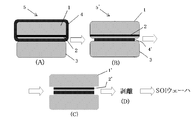
- the present invention forms an ion-implanted layer 2 by ion-implanting at least one gas ion of hydrogen or a rare gas from the surface of a bond wafer 1 made of a silicon single crystal, as shown in FIG.
- the bonded wafer 5 is bonded to the ion-implanted surface of the bond wafer 1 and the surface of the base wafer 3 via the insulating film 4 (FIG. 1A).
- the insulating film 4 positioned between the bond wafer 1 and the base wafer 3 is immersed in a liquid in which the insulating film 4 can be dissolved or exposed to a gas in which the insulating film 4 can be dissolved.
- Etching from the end toward the center forms an insulating film 4 ′ after etching the insulating film (FIG. 1B), and then the bond wafer 1 is peeled off by the ion implantation layer 2 (FIG. 1C). Having a degree, a method for manufacturing an SOI wafer.
- the bonding of the bond wafer 1 and the base wafer 3 is preferably performed at room temperature.
- the wafers are bonded together without using an adhesive or the like.
- conventional ion implantation is performed by performing low-temperature heat treatment (for example, 400 ° C. or lower) that does not cause separation of the bond wafer 1 in the ion-implanted layer 2 and then etching the insulating film 4 without performing heat treatment thereafter. Separation of the bond wafer 1 at the stage before etching, which has been a concern when using the peeling method, can be prevented, and the terrace width can be controlled more accurately.
- etching the insulating film 4 there is a method of immersing the bonded wafer 5 in an etching solution in which the insulating film can be dissolved, or etching by exposing to vapor that can dissolve the insulating film.
- the insulating film at the bonding interface is eroded from the outer peripheral edge.
- the bond wafer and the base wafer are not bonded at the eroded portion. Therefore, when the bond wafer is peeled off after etching, the SOI layer is not transferred and becomes a terrace region.
- the SOI layer is transferred by peeling. That is, the etching erosion width can be set as the terrace width, and the width can be controlled by the etching conditions such as the etching time, the concentration of the etching solution used, and the temperature.
- the insulating film is an oxide film
- an HF aqueous solution is suitable as the etchant, but buffered hydrofluoric acid, HF / H 2 O 2 / CH 3 COOH aqueous solution, HF / HNO 3 aqueous solution, and the like can also be applied.
- phosphoric acid is preferably used.
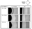
- a bonded wafer 24 is manufactured by bonding a bond wafer 22 with an oxide film 21 made of silicon single crystal and a base wafer 23 made of silicon single crystal at room temperature (25 ° C.). After the wafer 24 is immersed in an HF aqueous solution (25 ° C.) without being subjected to heat treatment, it is eroded from the outer peripheral edge of the oxide film on the bond wafer side due to a change in HF concentration and immersion time by peeling off the bonded surface (debonding) The micrograph which observed the condition is shown in FIG.
- the HF aqueous solution immersion conditions are 10% ⁇ 3 min, 50% ⁇ 30 min, 50% ⁇ 1 hr (HF aqueous solution concentration / immersion time).
- FIG. 3 shows that the terrace width varies depending on the concentration of the HF aqueous solution and the erosion time.
- the erosion width from the outer periphery of the insulating film during the above etching varies depending on the type of insulating film and the type / concentration / temperature of the etching solution. Under the same conditions, the erosion width is controlled by the etching time. Therefore, the terrace width after the SOI transfer can be easily controlled.
- SOI islands occur at the boundary between the SOI layer and the terrace. This is an area where the SOI layer is only partially transferred due to poor bonding strength due to poor flatness at the outer peripheral portion of the wafer to be bonded.
- the insulating film is etched to insulate the region where SOI islands are generated (for example, the range from 0.5 mm to 10 mm from the outer peripheral edge of the bonded wafer toward the center). If the erosion width of the film is widened so that the transfer of the SOI layer does not occur in a region where the bonding strength is low, which causes the generation of SOI islands, the SOI islands do not occur.
- control method of terrace width is not limited to ion implantation delamination method, and can be applied to the production of SOI by other bonding such as grinding and polishing method. It is.
- the insulating film is not particularly limited, but is generally an oxide film, a nitride film, or a laminated structure thereof.
- the method for manufacturing an SOI wafer of the present invention can be suitably used even in the case of bonding wafers in which the insulating film is a natural oxide film, that is, bonding between wafers having only a natural oxide film. Effective for control and suppression of SOI islands. Further, the bonding strength at room temperature can be improved by performing plasma treatment on the bonding surface before bonding.
- the bonded wafer 5 ′ (FIG. 2B) in which the insulating film 4 (FIG. 2A) of the bonded wafer 5 is etched by the above method is replaced with a silicon single crystal. Is immersed in a dissolvable liquid or exposed to a gas capable of dissolving a silicon single crystal, so that at least the outer periphery from the bonding interface side of the bond wafer 1 to at least the depth of the ion implantation layer 2 is etched. After the etching to the outer peripheral edge of the film 4 ′ (FIG. 2C), the bond wafer 1 can be peeled off (FIG. 2D). In FIG.
- 1 ′ represents a bond wafer after Si etching
- 2 ′ represents an ion implantation layer after Si etching.
- Si debris debris generated due to blistering caused by heat treatment on the ion-implanted layer on the outer periphery of the bond wafer from adhering to the terrace portion of the SOI wafer.
- the attached Si dust since the attached Si dust is not bonded to the base wafer like SOI island, it can be removed to some extent by general cleaning, but it is difficult to completely remove, so the adhesion of Si waste. It is desirable to suppress as much as possible.
- the liquid in which the silicon single crystal can be dissolved examples include a TMAH (tetramethylammonium hydroxide) aqueous solution.
- TMAH tetramethylammonium hydroxide
- the liquid can dissolve the silicon single crystal or the gas in which the silicon single crystal can be dissolved, It is not limited to this.
- the outer periphery of the bond wafer and the base wafer is not etched outside the desired range where Si etching is performed from the bonding interface side of the bond wafer to at least the depth of the ion implantation layer. It is preferable to protect by masking in advance.
- Example 1 Hydrogen ions are implanted under the ion implantation conditions shown in Table 1 below into a bond wafer in which a 150 nm thermal oxide film is formed on the surface of a 300 mm diameter silicon single crystal wafer, and bonded to a base wafer made of a 300 mm diameter silicon single crystal at room temperature. After bonding and bonding, the wafer was immersed in a 50% HF aqueous solution for 30 minutes, and then peeled and heat treated at 500 ° C. for 30 minutes to peel off the bond wafer to produce an SOI wafer. Table 1 shows the results of observing the SOI wafer fabrication conditions and the terrace portion after peeling the bond wafer with an optical microscope.
- the terrace width was 1.6 mm, and the generation of SOI islands was not observed, but Si debris generated due to blistering that occurred in the ion implantation layer on the outer periphery of the bond wafer during the peeling heat treatment occurred in the terrace portion. Adhesion was observed.
- Example 2 Bond wafer and base wafer are bonded together under the same conditions as in Example 1. After bonding, the wafer is immersed in a 50% HF aqueous solution for 1 hour, and then immersed in a TMAH aqueous solution. As shown in FIG. 2 (C), the outer periphery of the bond wafer. was etched from the bonding interface to a depth of 2 ⁇ m, and then a heat treatment for peeling off at 500 ° C. for 30 minutes to peel off the bond wafer to produce an SOI wafer. Table 1 shows the results of observing the SOI wafer fabrication conditions and the terrace after peeling with an optical microscope. The terrace width was 1.8 mm, and the occurrence of SOI islands was not observed. Moreover, no adhesion of Si scraps to the terrace portion occurred.
- Hydrogen ions are implanted under the ion implantation conditions shown in Table 1 below into a bond wafer in which a 150 nm thermal oxide film is formed on the surface of a 300 mm diameter silicon single crystal wafer, and bonded to a base wafer made of a 300 mm diameter silicon single crystal at room temperature. After that, peeling heat treatment was performed at 500 ° C. for 30 minutes, and the bond wafer was peeled off to produce an SOI wafer.
- Table 1 shows the results of observing the SOI wafer fabrication conditions and the terrace portion after peeling the bond wafer with an optical microscope. The terrace width was 1.4 mm, and generation of SOI islands and adhesion of Si debris were observed.
- Example 1 and Example 2 it was possible to control the terrace width by the etching time, and furthermore, it was possible to prevent the generation of SOI islands, which is a defect peculiar to the ion implantation delamination method. .
- adhesion of Si scraps could be completely prevented.
- production of SOI island and adhesion of Si waste were observed.
- the present invention is not limited to the above embodiment.
- the above-described embodiment is an exemplification, and the present invention has any configuration that has substantially the same configuration as the technical idea described in the claims of the present invention and that exhibits the same effects. It is contained in the technical range.
Abstract
Description
The present invention relates to a method for manufacturing an SOI wafer using a so-called ion implantation separation method, in which an ion-implanted wafer is peeled off after being bonded to manufacture an SOI wafer.
このように、ボンドウェーハとベースウェーハの間に位置する絶縁膜を、貼り合わせウェーハの外周端から中心方向へエッチングすることにより、テラス幅を制御することができ、イオン注入剥離法により剥離した場合に特有の欠陥であるSOI島の発生を防止することができる。 In order to solve the above-described problem, according to the present invention, an ion implantation layer is formed by ion-implanting at least one kind of gas ions of hydrogen or a rare gas from the surface of a bond wafer made of a silicon single crystal. In the method for manufacturing an SOI wafer in which an ion-implanted surface of a wafer and a surface of a base wafer are bonded to each other through an insulating film, and an SOI wafer is manufactured by peeling a bond wafer with the ion-implanted layer. The bonded wafer before peeling off the bond wafer is immersed in a liquid in which the insulating film can be dissolved or exposed to a gas in which the insulating film can be dissolved, so that the wafer is positioned between the bond wafer and the base wafer. Etching the insulating film from the outer peripheral edge of the bonded wafer toward the center. It provides a method for manufacturing an SOI wafer, comprising.
In this way, by etching the insulating film located between the bond wafer and the base wafer from the outer peripheral edge of the bonded wafer to the center direction, the terrace width can be controlled, and when peeling by the ion implantation peeling method It is possible to prevent the occurrence of SOI islands, which are defects specific to the.
このように、ボンドウェーハとベースウェーハの貼り合わせを室温で行うことによって、接着剤などを用いることなくウェーハ同士を接着させることができる。更に、その後熱処理を行うことなく、絶縁膜のエッチングを行うことによって、絶縁膜のエッチング前にイオン注入層でボンドウェーハが剥離してしまうことを防ぐことができ、また、より正確にテラス幅を制御することができ、SOI島を防止することができる。 The bonding wafer and the base wafer are preferably bonded at room temperature, and then the insulating film is etched without performing a heat treatment.
Thus, by bonding the bond wafer and the base wafer at room temperature, the wafers can be bonded to each other without using an adhesive or the like. Furthermore, by performing etching of the insulating film without performing heat treatment after that, it is possible to prevent the bond wafer from being peeled off by the ion implantation layer before etching of the insulating film, and more accurately to increase the terrace width. Can be controlled and can prevent SOI islands.
このように、ボンドウェーハとベースウェーハの貼り合わせを室温で行い、その後イオン注入層において剥離が発生しない低温熱処理を行った後に、絶縁膜のエッチングを行うことで、より正確にテラス幅を制御することができ、SOI島を防止することができる。 The bonding wafer and the base wafer are preferably bonded at room temperature, and then the insulating film is etched after performing a low-temperature heat treatment that does not cause separation in the ion-implanted layer.
As described above, the bonding of the bond wafer and the base wafer is performed at room temperature, and then the low-temperature heat treatment that does not cause separation in the ion-implanted layer is performed, and then the insulating film is etched to control the terrace width more accurately. And can prevent SOI islands.
このように、絶縁膜のエッチングを、貼り合わせウェーハの外周端から中心方向へ0.5mm以上10mm以下の範囲内で行うことによって、テラス部にレーザーマーク等をデバイス工程で作製する場合に、適当なテラス幅を得ることができ、また、SOI島の発生をより確実に防止することができる。 Moreover, it is preferable to etch the insulating film within a range of 0.5 mm or more and 10 mm or less from the outer peripheral edge of the bonded wafer toward the center.
As described above, when the insulating film is etched within the range of 0.5 mm or more and 10 mm or less from the outer peripheral edge of the bonded wafer to the center direction, it is suitable for manufacturing a laser mark or the like on the terrace portion in the device process. It is possible to obtain a wide terrace width and more reliably prevent the occurrence of SOI islands.
このようなSiエッチングにより、デバイス作製工程で異物となりうる部分を予め除去することができる。 In addition, the bonded wafer on which the insulating film has been etched is immersed in a liquid in which the silicon single crystal can be dissolved, or is exposed to a gas in which the silicon single crystal can be dissolved. It is preferable that the bond wafer is peeled after etching the outer peripheral edge from the mating surface side to at least the depth of the ion implantation layer to at least the outer peripheral edge of the etched insulating film (hereinafter referred to as Si etching).
By such Si etching, a portion that can be a foreign substance in the device manufacturing process can be removed in advance.
As described above, by using the SOI wafer manufacturing method of the present invention, the terrace width can be controlled, and the occurrence of SOI islands, which are peculiar defects when peeling by the ion implantation peeling method, can be prevented. it can.
絶縁膜が酸化膜の場合、エッチング液としてはHF水溶液が好適であるが、バッファードフッ酸、HF/H2O2/CH3COOH水溶液、HF/HNO3水溶液なども適用できる。また、窒化膜の場合は、リン酸を用いることが好ましい。 As a method of etching the insulating
In the case where the insulating film is an oxide film, an HF aqueous solution is suitable as the etchant, but buffered hydrofluoric acid, HF / H 2 O 2 / CH 3 COOH aqueous solution, HF / HNO 3 aqueous solution, and the like can also be applied. In the case of a nitride film, phosphoric acid is preferably used.
図3より、HF水溶液の濃度及び浸食時間により、テラス幅が異なるのがわかる。 As shown in FIG. 4, a bonded
FIG. 3 shows that the terrace width varies depending on the concentration of the HF aqueous solution and the erosion time.
このようにボンドウェーハ1の貼り合わせ界面側から少なくともイオン注入層2の深さまでの外周部を、少なくともエッチングされた絶縁膜4’の外周端までSiエッチングすることによって、デバイス作製工程で異物となりうる箇所を予め除去することができる。こうすることで、SOI島の発生が確実に防止されることとなる。また、ボンドウェーハ外周部のイオン注入層が除去されることになるため、後工程で熱処理が加わっても外周部でのブリスタリングが発生しなくなる。従って、ボンドウェーハ外周部のイオン注入層に熱処理が加わることによって生ずるブリスタリングに起因して発生するSi屑(くず)がSOIウェーハのテラス部に付着することを防ぐことができる。尚、付着したSi屑はSOI島の様にベースウェーハに結合したものではないため、一般的な洗浄によってある程度除去することができるが、完全に除去することは困難であるため、Si屑の付着もできる限り抑制することが望ましい。 Further, as shown in FIG. 2, the bonded
Thus, by etching the outer peripheral portion from the bonding interface side of the
また、このようなSiエッチングを行う前に、ボンドウェーハの貼り合わせ界面側から少なくともイオン注入層の深さまでのSiエッチングを施す所望範囲以外の外周は、ボンドウェーハ及びベースウェーハの外周がエッチングされないように予めマスクして保護しておくことが好ましい。
Examples of the liquid in which the silicon single crystal can be dissolved include a TMAH (tetramethylammonium hydroxide) aqueous solution. However, if the liquid can dissolve the silicon single crystal or the gas in which the silicon single crystal can be dissolved, It is not limited to this.
Further, before performing such Si etching, the outer periphery of the bond wafer and the base wafer is not etched outside the desired range where Si etching is performed from the bonding interface side of the bond wafer to at least the depth of the ion implantation layer. It is preferable to protect by masking in advance.
直径300mmのシリコン単結晶ウェーハの表面に150nmの熱酸化膜を作製したボンドウェーハに、水素イオンを下記表1のイオン注入条件で注入し、直径300mmのシリコン単結晶からなるベースウェーハと室温で貼り合わせ、貼り合わせ後に50%HF水溶液に30分浸漬し、その後、500℃で30分間剥離熱処理してボンドウェーハを剥離してSOIウェーハを作製した。SOIウェーハ作製条件及びボンドウェーハの剥離後のテラス部を光学顕微鏡で観察した結果を表1に示す。
テラス幅は、1.6mmとなり、SOI島の発生は観察されなかったが、剥離熱処理時にボンドウェーハの外周部のイオン注入層に生じたブリスタリングに起因して発生したSi屑が、テラス部に付着しているのが観察された。
Example 1
Hydrogen ions are implanted under the ion implantation conditions shown in Table 1 below into a bond wafer in which a 150 nm thermal oxide film is formed on the surface of a 300 mm diameter silicon single crystal wafer, and bonded to a base wafer made of a 300 mm diameter silicon single crystal at room temperature. After bonding and bonding, the wafer was immersed in a 50% HF aqueous solution for 30 minutes, and then peeled and heat treated at 500 ° C. for 30 minutes to peel off the bond wafer to produce an SOI wafer. Table 1 shows the results of observing the SOI wafer fabrication conditions and the terrace portion after peeling the bond wafer with an optical microscope.
The terrace width was 1.6 mm, and the generation of SOI islands was not observed, but Si debris generated due to blistering that occurred in the ion implantation layer on the outer periphery of the bond wafer during the peeling heat treatment occurred in the terrace portion. Adhesion was observed.
実施例1と同様の条件でボンドウェーハとベースウェーハを貼り合わせ、貼り合わせ後に50%HF水溶液に1時間浸漬し、その後TMAH水溶液に浸漬し、図2(C)の様にボンドウエーハの外周部を貼り合わせ界面から2μmの深さまでSiエッチングし、その後500℃で30分間剥離熱処理してボンドウェーハを剥離してSOIウェーハを作製した。SOIウェーハ作製条件及び剥離後のテラス部を光学顕微鏡で観察した結果を表1に示す。
テラス幅は、1.8mmとなり、SOI島の発生は観察されなかった。また、Si屑のテラス部への付着も全く発生していなかった。
(Example 2)
Bond wafer and base wafer are bonded together under the same conditions as in Example 1. After bonding, the wafer is immersed in a 50% HF aqueous solution for 1 hour, and then immersed in a TMAH aqueous solution. As shown in FIG. 2 (C), the outer periphery of the bond wafer. Was etched from the bonding interface to a depth of 2 μm, and then a heat treatment for peeling off at 500 ° C. for 30 minutes to peel off the bond wafer to produce an SOI wafer. Table 1 shows the results of observing the SOI wafer fabrication conditions and the terrace after peeling with an optical microscope.
The terrace width was 1.8 mm, and the occurrence of SOI islands was not observed. Moreover, no adhesion of Si scraps to the terrace portion occurred.
直径300mmのシリコン単結晶ウェーハの表面に150nmの熱酸化膜を作製したボンドウェーハに、水素イオンを下記表1のイオン注入条件で注入し、直径300mmのシリコン単結晶からなるベースウェーハと室温で貼り合わせ、その後、500℃で30分剥離熱処理してボンドウェーハを剥離してSOIウェーハを作製した。SOIウェーハ作製条件及びボンドウェーハ剥離後のテラス部を光学顕微鏡で観察した結果を表1に示す。
テラス幅は1.4mmとなり、SOI島の発生とSi屑の付着が観察された。 (Comparative example)
Hydrogen ions are implanted under the ion implantation conditions shown in Table 1 below into a bond wafer in which a 150 nm thermal oxide film is formed on the surface of a 300 mm diameter silicon single crystal wafer, and bonded to a base wafer made of a 300 mm diameter silicon single crystal at room temperature. After that, peeling heat treatment was performed at 500 ° C. for 30 minutes, and the bond wafer was peeled off to produce an SOI wafer. Table 1 shows the results of observing the SOI wafer fabrication conditions and the terrace portion after peeling the bond wafer with an optical microscope.
The terrace width was 1.4 mm, and generation of SOI islands and adhesion of Si debris were observed.

Claims (7)
- シリコン単結晶からなるボンドウェーハの表面から水素または希ガスのうち少なくとも1種類のガスイオンをイオン注入してイオン注入層を形成し、該ボンドウェーハのイオン注入した表面とベースウェーハの表面とを絶縁膜を介して貼り合わせ、前記イオン注入層でボンドウェーハを剥離することによりSOIウェーハを作製するSOIウェーハの製造方法において、
前記イオン注入層でボンドウェーハを剥離する前の貼り合わせウェーハを、前記絶縁膜が溶解可能な液体に浸漬するか、前記絶縁膜が溶解可能な気体に曝すことによって、前記ボンドウェーハと前記ベースウェーハの間に位置する前記絶縁膜を、前記貼り合わせウェーハの外周端から中心方向へエッチングする工程を有することを特徴とするSOIウェーハの製造方法。
At least one kind of gas ions of hydrogen or rare gas is ion-implanted from the surface of a bond wafer made of silicon single crystal to form an ion-implanted layer, and the surface of the bond wafer and the surface of the base wafer are insulated. In a method for manufacturing an SOI wafer in which an SOI wafer is manufactured by laminating through a film and peeling the bond wafer with the ion-implanted layer,
The bonded wafer and the base wafer can be obtained by immersing the bonded wafer before peeling the bond wafer with the ion-implanted layer in a liquid in which the insulating film can be dissolved or by exposing the bonded wafer to a gas in which the insulating film can be dissolved. A method of manufacturing an SOI wafer, comprising: a step of etching the insulating film positioned between the outer peripheral edge and the center of the bonded wafer.
- 前記ボンドウェーハとベースウェーハの貼り合わせを室温で行い、その後、熱処理を行うことなく、前記絶縁膜のエッチングを行うことを特徴とする請求項1に記載のSOIウェーハの製造方法。
The method for manufacturing an SOI wafer according to claim 1, wherein the bonding wafer and the base wafer are bonded at room temperature, and then the insulating film is etched without performing a heat treatment.
- 前記ボンドウェーハとベースウェーハの貼り合わせを室温で行い、その後、前記イオン注入層において剥離が発生しない低温熱処理を行った後に、前記絶縁膜のエッチングを行うことを特徴とする請求項1に記載のSOIウェーハの製造方法。
2. The insulating film is etched according to claim 1, wherein the bonding wafer and the base wafer are bonded together at room temperature, and then the insulating film is etched after performing low-temperature heat treatment that does not cause separation in the ion-implanted layer. Manufacturing method of SOI wafer.
- 前記絶縁膜のエッチングを、前記貼り合わせウェーハの外周端から中心方向へ0.5mm以上10mm以下の範囲内で行うことを特徴とする請求項1乃至請求項3のいずれか一項に記載のSOIウェーハの製造方法。
4. The SOI according to claim 1, wherein the insulating film is etched within a range from 0.5 mm to 10 mm from an outer peripheral edge of the bonded wafer toward a center. 5. Wafer manufacturing method.
- 前記絶縁膜のエッチングを、前記絶縁膜が酸化膜、窒化膜、又はこれらの積層構造である貼り合わせウェーハを用い、該貼り合わせウェーハをHF含有水溶液またはリン酸に浸積することによって行うことを特徴とする請求項1乃至請求項4のいずれか一項に記載のSOIウェーハの製造方法。
Etching of the insulating film is performed by using a bonded wafer in which the insulating film is an oxide film, a nitride film, or a laminated structure thereof, and immersing the bonded wafer in an HF-containing aqueous solution or phosphoric acid. 5. The method for manufacturing an SOI wafer according to claim 1, wherein the SOI wafer is manufactured as follows.
- 前記絶縁膜のエッチングを、前記絶縁膜が自然酸化膜である貼り合わせウェーハを用いて行うことを特徴とする請求項1乃至請求項5のいずれか一項に記載のSOIウェーハの製造方法。
6. The method for manufacturing an SOI wafer according to claim 1, wherein the insulating film is etched using a bonded wafer in which the insulating film is a natural oxide film.
- 前記絶縁膜のエッチングが行われた前記貼り合わせウェーハを、前記シリコン単結晶が溶解可能な液体に浸漬するか、前記シリコン単結晶が溶解可能な気体に曝すことによって、前記ボンドウェーハの貼り合わせ面側から少なくとも前記イオン注入層の深さまでの外周端部を、少なくとも前記エッチングされた絶縁膜の外周端までエッチングした後、前記ボンドウェーハの剥離を行うことを特徴とする請求項1乃至請求項6のいずれか一項に記載のSOIウェーハの製造方法。
The bonded surface of the bond wafer is obtained by immersing the bonded wafer on which the insulating film has been etched in a liquid in which the silicon single crystal can be dissolved or by exposing the bonded wafer to a gas in which the silicon single crystal can be dissolved. 7. The bond wafer is peeled off after etching an outer peripheral end from the side to at least the depth of the ion-implanted layer to at least an outer peripheral end of the etched insulating film. The manufacturing method of the SOI wafer as described in any one of these.
Priority Applications (3)
| Application Number | Priority Date | Filing Date | Title |
|---|---|---|---|
| EP10745896.0A EP2402983B1 (en) | 2009-02-26 | 2010-01-08 | Method for manufacturing soi wafer |
| US13/145,275 US20110281420A1 (en) | 2009-02-26 | 2010-01-08 | Method for manufacturing soi wafer |
| CN2010800086820A CN102326227A (en) | 2009-02-26 | 2010-01-08 | The manufacturing approach of SOI wafer |
Applications Claiming Priority (2)
| Application Number | Priority Date | Filing Date | Title |
|---|---|---|---|
| JP2009043403A JP5244650B2 (en) | 2009-02-26 | 2009-02-26 | Manufacturing method of SOI wafer |
| JP2009-043403 | 2009-02-26 |
Publications (1)
| Publication Number | Publication Date |
|---|---|
| WO2010098007A1 true WO2010098007A1 (en) | 2010-09-02 |
Family
ID=42665227
Family Applications (1)
| Application Number | Title | Priority Date | Filing Date |
|---|---|---|---|
| PCT/JP2010/000076 WO2010098007A1 (en) | 2009-02-26 | 2010-01-08 | Method for manufacturing soi wafer |
Country Status (6)
| Country | Link |
|---|---|
| US (1) | US20110281420A1 (en) |
| EP (1) | EP2402983B1 (en) |
| JP (1) | JP5244650B2 (en) |
| KR (1) | KR20110116036A (en) |
| CN (1) | CN102326227A (en) |
| WO (1) | WO2010098007A1 (en) |
Cited By (4)
| Publication number | Priority date | Publication date | Assignee | Title |
|---|---|---|---|---|
| US8192822B2 (en) | 2008-03-31 | 2012-06-05 | Memc Electronic Materials, Inc. | Edge etched silicon wafers |
| CN103299395A (en) * | 2010-12-20 | 2013-09-11 | 信越半导体股份有限公司 | Method for manufacturing SOI wafer |
| US8735261B2 (en) | 2008-11-19 | 2014-05-27 | Memc Electronic Materials, Inc. | Method and system for stripping the edge of a semiconductor wafer |
| US8853054B2 (en) | 2012-03-06 | 2014-10-07 | Sunedison Semiconductor Limited | Method of manufacturing silicon-on-insulator wafers |
Families Citing this family (6)
| Publication number | Priority date | Publication date | Assignee | Title |
|---|---|---|---|---|
| JP5978764B2 (en) | 2012-05-24 | 2016-08-24 | 信越半導体株式会社 | Manufacturing method of SOI wafer |
| JP5862521B2 (en) * | 2012-09-03 | 2016-02-16 | 信越半導体株式会社 | Manufacturing method of SOI wafer |
| JP6056516B2 (en) * | 2013-02-01 | 2017-01-11 | 信越半導体株式会社 | Manufacturing method of SOI wafer and SOI wafer |
| US9177967B2 (en) | 2013-12-24 | 2015-11-03 | Intel Corporation | Heterogeneous semiconductor material integration techniques |
| CN105280541A (en) * | 2015-09-16 | 2016-01-27 | 中国电子科技集团公司第五十五研究所 | Temporary bonding method and bonding-removing method for ultrathin semiconductor wafer |
| FR3076393A1 (en) * | 2017-12-28 | 2019-07-05 | Commissariat A L'energie Atomique Et Aux Energies Alternatives | METHOD OF TRANSFERRING A USEFUL LAYER |
Citations (5)
| Publication number | Priority date | Publication date | Assignee | Title |
|---|---|---|---|---|
| JPH1070054A (en) | 1997-07-19 | 1998-03-10 | Shin Etsu Handotai Co Ltd | Manufacture of junction wafer |
| JPH11121310A (en) * | 1997-10-09 | 1999-04-30 | Denso Corp | Manufacture of semiconductor substrate |
| JP2002305292A (en) | 2001-04-06 | 2002-10-18 | Shin Etsu Handotai Co Ltd | Soi wafer and method of manufacturing the same |
| JP2007141946A (en) * | 2005-11-15 | 2007-06-07 | Sumco Corp | Method of manufacturing soi substrate, and soi substrate manufactured by same |
| JP2008526038A (en) * | 2004-12-28 | 2008-07-17 | コミツサリア タ レネルジー アトミーク | Method for trimming a structure obtained by assembly of two wafers |
Family Cites Families (4)
| Publication number | Priority date | Publication date | Assignee | Title |
|---|---|---|---|---|
| US6534380B1 (en) * | 1997-07-18 | 2003-03-18 | Denso Corporation | Semiconductor substrate and method of manufacturing the same |
| DE69917819T2 (en) * | 1998-02-04 | 2005-06-23 | Canon K.K. | SOI substrate |
| JP4313874B2 (en) * | 1999-02-02 | 2009-08-12 | キヤノン株式会社 | Substrate manufacturing method |
| KR101151458B1 (en) * | 2005-02-28 | 2012-06-01 | 신에쯔 한도타이 가부시키가이샤 | Method for manufacturing bonded wafer and bonded wafer |
-
2009
- 2009-02-26 JP JP2009043403A patent/JP5244650B2/en active Active
-
2010
- 2010-01-08 EP EP10745896.0A patent/EP2402983B1/en active Active
- 2010-01-08 US US13/145,275 patent/US20110281420A1/en not_active Abandoned
- 2010-01-08 CN CN2010800086820A patent/CN102326227A/en active Pending
- 2010-01-08 KR KR1020117019761A patent/KR20110116036A/en not_active Application Discontinuation
- 2010-01-08 WO PCT/JP2010/000076 patent/WO2010098007A1/en active Application Filing
Patent Citations (5)
| Publication number | Priority date | Publication date | Assignee | Title |
|---|---|---|---|---|
| JPH1070054A (en) | 1997-07-19 | 1998-03-10 | Shin Etsu Handotai Co Ltd | Manufacture of junction wafer |
| JPH11121310A (en) * | 1997-10-09 | 1999-04-30 | Denso Corp | Manufacture of semiconductor substrate |
| JP2002305292A (en) | 2001-04-06 | 2002-10-18 | Shin Etsu Handotai Co Ltd | Soi wafer and method of manufacturing the same |
| JP2008526038A (en) * | 2004-12-28 | 2008-07-17 | コミツサリア タ レネルジー アトミーク | Method for trimming a structure obtained by assembly of two wafers |
| JP2007141946A (en) * | 2005-11-15 | 2007-06-07 | Sumco Corp | Method of manufacturing soi substrate, and soi substrate manufactured by same |
Cited By (5)
| Publication number | Priority date | Publication date | Assignee | Title |
|---|---|---|---|---|
| US8192822B2 (en) | 2008-03-31 | 2012-06-05 | Memc Electronic Materials, Inc. | Edge etched silicon wafers |
| US8309464B2 (en) | 2008-03-31 | 2012-11-13 | Memc Electronic Materials, Inc. | Methods for etching the edge of a silicon wafer |
| US8735261B2 (en) | 2008-11-19 | 2014-05-27 | Memc Electronic Materials, Inc. | Method and system for stripping the edge of a semiconductor wafer |
| CN103299395A (en) * | 2010-12-20 | 2013-09-11 | 信越半导体股份有限公司 | Method for manufacturing SOI wafer |
| US8853054B2 (en) | 2012-03-06 | 2014-10-07 | Sunedison Semiconductor Limited | Method of manufacturing silicon-on-insulator wafers |
Also Published As
| Publication number | Publication date |
|---|---|
| CN102326227A (en) | 2012-01-18 |
| JP5244650B2 (en) | 2013-07-24 |
| EP2402983A1 (en) | 2012-01-04 |
| JP2010199353A (en) | 2010-09-09 |
| EP2402983B1 (en) | 2015-11-25 |
| KR20110116036A (en) | 2011-10-24 |
| US20110281420A1 (en) | 2011-11-17 |
| EP2402983A4 (en) | 2012-07-25 |
Similar Documents
| Publication | Publication Date | Title |
|---|---|---|
| JP5244650B2 (en) | Manufacturing method of SOI wafer | |
| JP5135935B2 (en) | Manufacturing method of bonded wafer | |
| JP4421652B2 (en) | Manufacturing method of SOI wafer | |
| US8288251B2 (en) | Method for preparing SOI substrate having backside sandblasted | |
| WO2002084738A1 (en) | Soi wafer and its manufacturing method | |
| JP2010538459A (en) | Reuse of semiconductor wafers in delamination processes using heat treatment | |
| CN107615445B (en) | Method for manufacturing silicon wafer on insulator | |
| JP2011103409A (en) | Wafer laminating method | |
| JP2008016534A (en) | Manufacturing method of laminated wafer | |
| KR101910100B1 (en) | Method for manufacturing soi wafer | |
| JP5978764B2 (en) | Manufacturing method of SOI wafer | |
| KR20160023712A (en) | Method for manufacturing bonded wafer | |
| JP5862521B2 (en) | Manufacturing method of SOI wafer | |
| JP2010092909A (en) | Method of manufacturing soi wafer | |
| JP2008235495A (en) | Soi (silicon on insulator) wafer and manufacturing method therefor | |
| WO2015056386A1 (en) | Bonded wafer manufacturing method | |
| KR20160052551A (en) | Bonded wafer manufacturing method |
Legal Events
| Date | Code | Title | Description |
|---|---|---|---|
| WWE | Wipo information: entry into national phase |
Ref document number: 201080008682.0 Country of ref document: CN |
|
| 121 | Ep: the epo has been informed by wipo that ep was designated in this application |
Ref document number: 10745896 Country of ref document: EP Kind code of ref document: A1 |
|
| WWE | Wipo information: entry into national phase |
Ref document number: 13145275 Country of ref document: US |
|
| WWE | Wipo information: entry into national phase |
Ref document number: 2010745896 Country of ref document: EP |
|
| ENP | Entry into the national phase |
Ref document number: 20117019761 Country of ref document: KR Kind code of ref document: A |
|
| NENP | Non-entry into the national phase |
Ref country code: DE |