WO2010092892A1 - 吸光分析装置 - Google Patents
吸光分析装置 Download PDFInfo
- Publication number
- WO2010092892A1 WO2010092892A1 PCT/JP2010/051541 JP2010051541W WO2010092892A1 WO 2010092892 A1 WO2010092892 A1 WO 2010092892A1 JP 2010051541 W JP2010051541 W JP 2010051541W WO 2010092892 A1 WO2010092892 A1 WO 2010092892A1
- Authority
- WO
- WIPO (PCT)
- Prior art keywords
- light
- optical
- wavelength
- input
- semiconductor optical
- Prior art date
- Legal status (The legal status is an assumption and is not a legal conclusion. Google has not performed a legal analysis and makes no representation as to the accuracy of the status listed.)
- Ceased
Links
Images









Classifications
-
- G—PHYSICS
- G01—MEASURING; TESTING
- G01N—INVESTIGATING OR ANALYSING MATERIALS BY DETERMINING THEIR CHEMICAL OR PHYSICAL PROPERTIES
- G01N21/00—Investigating or analysing materials by the use of optical means, i.e. using sub-millimetre waves, infrared, visible or ultraviolet light
- G01N21/17—Systems in which incident light is modified in accordance with the properties of the material investigated
- G01N21/25—Colour; Spectral properties, i.e. comparison of effect of material on the light at two or more different wavelengths or wavelength bands
- G01N21/31—Investigating relative effect of material at wavelengths characteristic of specific elements or molecules, e.g. atomic absorption spectrometry
- G01N21/39—Investigating relative effect of material at wavelengths characteristic of specific elements or molecules, e.g. atomic absorption spectrometry using tunable lasers
Definitions
- the present invention relates to an absorption spectrometer using a semiconductor optical amplifier having a negative feedback amplification function.
- An optical analyzer using a so-called cavity ring-down method is known as an apparatus for analyzing a sample using the light absorption characteristics of a light-transmitting substance.
- a laser beam of a predetermined wavelength for example, having a frequency of about several tens of kHz is circulated in an annular propagation path or provided between mirrors in a propagation path configured in a closed system.
- the ring-down time which is the time from the attenuation waveform signal until the light intensity of the pulsed laser beam attenuates to 1 / e, is short and cannot be obtained accurately, or the attenuation rate is also accurately accurate. Since it was not obtained, sufficient measurement accuracy was not obtained.
- the present invention has been made against the background of the above circumstances, and an object of the present invention is to provide an absorption spectrometer capable of measuring stably with high measurement accuracy.
- the present inventors have negatively charged a part of the light detected by the photodetector, that is, the light in the light propagation path extracted from the closed system propagation path.
- the fact that amplification using an optical amplifier having a feedback amplification function improves the S / N ratio at the same time, and at the same time, does not oscillate in the closed propagation path and enables high-accuracy and stable absorption analysis. I found.
- the present invention has been made based on such knowledge.
- the invention according to claim 1 for achieving the above object includes: (a) a laser light source that outputs a pulsed laser beam having a predetermined wavelength; and (b) a closed system that repeatedly propagates light by reciprocating or reciprocating. An optical waveguide having a propagation path; and (c) a pulse-shaped output provided from the laser light source by optically coupling the laser light source and the optical waveguide provided in a closed propagation path of the optical waveguide.
- An optical coupler device that inputs laser light into the closed propagation path of the optical waveguide and extracts a part of the pulsed laser light that repeatedly propagates in the closed propagation path; and (d) the optical coupler device A photodetector for detecting a part of the pulsed laser light extracted from within the closed-system propagation path of the optical waveguide; and (e) provided in the closed-system propagation path of the optical waveguide in a state in which a sample is accommodated.
- a sample storage device for repeatedly propagating the pulsed laser light through the sample in the closed system propagation path, based on the attenuation rate of a part of the intensity of the pulsed laser light detected by the photodetector (F) ⁇ ⁇ receiving a part of pulsed laser light propagating in the optical waveguide taken out from the optical coupler device as input light, and the input light is negative
- a negative feedback amplification type semiconductor optical amplifier that outputs the feedback amplified output light to the photodetector is provided between the optical coupler device and the photodetector.
- a negative feedback amplification type semiconductor optical amplifier is provided between the optical coupler device and the photodetector, and the negative feedback amplification type semiconductor optical amplifier includes the light Receiving a part of the pulsed laser light propagating in the optical waveguide taken out from the coupler apparatus as input light, and outputting the output light obtained by negative feedback amplification of the input light to the photodetector,
- the light detected by the photodetector has a reduced waveform distortion and an increased S / N ratio by negative feedback amplification. For this reason, there is no oscillation in the closed propagation path and stable absorption analysis is possible.
- the S / N ratio of the observed waveform in which the light intensity of the pulsed laser light decays with time is high and the noise contained in the waveform is reduced, the light intensity of the pulsed laser light from such a signal. Since the time until the dampens, that is, the ring-down time, can be obtained accurately and accurately, the measurement accuracy for the attenuation of the attenuation curve can be sufficiently obtained.
- the S / N ratio of the observed waveform in which the light intensity of the pulsed laser light decays with time is high and the noise contained in the waveform is reduced, the light intensity of the pulsed laser light from such a signal. Since the time until the dampens, that is, the ring-down time, can be obtained accurately and accurately, the measurement accuracy for the attenuation of the attenuation curve can be sufficiently obtained.
- the negative feedback amplification type semiconductor optical amplifier amplifies and outputs the first input light which is a part of the pulsed laser light having the predetermined wavelength
- the pulse A first semiconductor optical amplifying element that emits first ambient light other than the wavelength of the pulsed laser light, the intensity of which is inverted with respect to the intensity of the laser light, and the light output from the first semiconductor optical amplifying element
- a first wavelength selection element that selects all or part of one ambient light; all or part of the first ambient light selected by the first wavelength selection element; and
- the second input light which is a part of the pulsed laser light extracted from the closed propagation path, is input, has the wavelength of the second input light, and is intensity-modulated by the ambient light of the first input light.
- the output light Of the light emitted from the semiconductor optical amplifying element and the second semiconductor optical amplifying element to the output side the light having the wavelength of the second input light is transmitted, but the wavelength is different from the wavelength of the second input light.
- a second negative feedback amplification wavelength-selective reflecting element that reflects light and enters the second semiconductor optical amplifying element. If it does in this way, light will be reflected by the wavelength selective reflection element for 2nd negative feedback amplification to the wavelength different from the wavelength of the 2nd input light among the light radiated
- the second negative feedback amplification wavelength selective reflection element is an end of an output-side optical fiber optically coupled to an output side of the second semiconductor optical amplification element.
- a second optical fiber grating part that reflects all or part of the second ambient light emitted from the second semiconductor optical amplifier and re-enters the second semiconductor optical amplifier.
- the second negative feedback amplification wavelength-selective reflecting element is provided in the end of the output side optical fiber and is miniaturized, so that the absorption spectrometer is miniaturized.
- a tip lens is provided on an end surface of the end portion on the second semiconductor optical amplification element side where the second optical fiber grating portion of the output side optical fiber is provided,
- the output side optical fiber and the second semiconductor optical amplifying element are optically coupled directly via the tip lens.
- the second optical fiber grating section transmits light having the wavelength of the output light, and has a band of at least 3 nm or more generated by amplification of the second semiconductor optical amplification element.
- the second semiconductor optical amplifying element has a reflection characteristic that reflects all or a part of light in a short wavelength side and / or long wavelength side band with respect to the amplified light.
- they are arranged close to each other with a predetermined optical path length LL. In this way, the absorption spectrometer can be miniaturized.
- the predetermined optical path length LL is such that the refractive index of the optical transmission path between the second semiconductor optical amplification element and the first optical fiber grating portion is n,
- the speed of light is c (mm / sec) and the time interval of the pulses of the second input light is t (seconds)
- the negative feedback amplification type semiconductor optical amplifier is provided on an input side of the first semiconductor optical amplification element, and is input to the first semiconductor optical amplification element.
- First negative feedback that allows input light to pass but reflects all or part of the first ambient light emitted from the first semiconductor optical amplifier to the input side and re-inputs the first semiconductor optical amplifier to the first semiconductor optical amplifier.
- a wavelength selective reflecting element for amplification In this way, a negative feedback action can be obtained also in the first semiconductor optical amplification width element, and the S / N ratio is further increased with less waveform distortion.
- the first negative feedback amplification wavelength selective reflection element is provided at an end of an input optical fiber optically coupled to an input side of the first semiconductor optical amplification element.
- a first optical fiber grating portion that is provided and reflects all or a part of the first ambient light emitted from the first semiconductor optical amplifying element and re-enters the first semiconductor optical amplifying element;
- the first negative feedback amplification wavelength selective reflection element is provided in the end portion of the output light side fiber 39 and is miniaturized, so that the absorption spectrometer is miniaturized.
- a tip ball lens is provided on each end surface of the input optical fiber provided with the first optical fiber grating portion on the first semiconductor optical amplification element side.
- the input optical fiber and the first semiconductor optical amplifying element are directly optically coupled via the tip ball lens.
- the coupling structure is further simplified and miniaturized, and the absorption spectrometer is miniaturized.
- the first optical fiber grating portion transmits light having a first wavelength of the first input light and is generated by amplification of the first semiconductor optical amplification element.
- the amplified light in the above band it has a reflection characteristic that reflects all or a part of the light on the shorter wavelength side and / or longer wavelength side than the wavelength of the first input light, and
- One semiconductor optical amplification element is arranged in close proximity with a predetermined optical path length LL. In this way, the absorption spectrometer is further downsized.
- the predetermined optical path length LL is such that the refractive index of the optical transmission path between the first semiconductor optical amplification element and the first optical fiber grating section is n, in vacuum LL ⁇ (c ⁇ t) / (20 ⁇ n) where c (mm / sec) is the speed of light and t (seconds) is the time interval of the pulses of the first input light.
- c (mm / sec) is the speed of light
- t (seconds) is the time interval of the pulses of the first input light.
- the negative feedback amplification type semiconductor optical amplifier is configured such that a part of the pulsed laser light extracted from the closed propagation path of the optical waveguide by the optical coupler device is the first.
- a second semiconductor optical amplifying element that is input as two-input light and outputs a negative feedback amplified output light having a wavelength of the second input light; and light emitted from the second semiconductor optical amplifying element to the output side Among them, the second negative feedback amplification wavelength that transmits light having the wavelength of the second input light, but reflects the light to a wavelength different from the wavelength of the second input light and enters the second semiconductor optical amplification element.
- a selective reflection element is configured such that a part of the pulsed laser light extracted from the closed propagation path of the optical waveguide by the optical coupler device is the first.
- the absorbance analyzer is configured more simply.
- FIG. 2 is a diagram for explaining a main part of a configuration example of the negative feedback amplification type semiconductor optical amplifier of FIG. 1. It is a perspective view explaining the structure of the 1st semiconductor optical amplifier element of FIG. 5, or the 2nd semiconductor optical amplifier element. It is a figure explaining the structural example of the 2nd fiber grating part provided in the edge part of the output side optical fiber of FIG. FIG.
- FIG. 6 is a diagram showing a spectrum of amplified control light Lc, that is, output light Lout that is selectively passed by the second optical fiber grating section of FIG. 5. It is a figure which shows the spectrum of 2nd ambient light Ls2 selectively reflected by the 2nd optical fiber grating part of FIG.
- FIG. 6 is a diagram illustrating a waveform of control light (second input light) Lc having a first wavelength ⁇ 1 used in an experiment using the second semiconductor optical amplifier of FIG. 5.
- FIG. 11 is a diagram illustrating ambient light that is reflected and re-input to the optical fiber grating portion when the input light illustrated in FIG. 10 is input in the second semiconductor optical amplifier of FIG. 5.
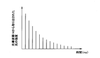
- FIG. 2 is a schematic diagram showing a partial attenuation waveform of pulsed laser light taken out from a closed system propagation path around which pulsed laser light is circulated in the absorption spectrometer of FIG. 1.
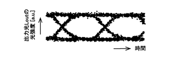
- FIG. 2 is an observation diagram showing a partial attenuation waveform of pulsed laser light extracted from a closed propagation path in the absorption spectrometer of FIG. 1. It is a figure explaining the principal part of the other structural example of the negative feedback amplification type semiconductor optical amplifier in other Example ( ⁇ ⁇ Example 2) of this invention. It is a figure explaining the principal part of the other structural example of the negative feedback amplification type semiconductor optical amplifier in other Example (Third Example 3) of the present invention. It is a figure explaining the principal part of the other structural example of the negative feedback amplification type
- FIG. 1 is a schematic diagram showing the main part of the configuration of an absorption spectrometer 10 according to an embodiment of the present invention.
- an absorption analyzer 10 includes (a) a laser light source 12 that outputs a pulsed laser beam L having a first wavelength ⁇ 1 of a predetermined wavelength, for example, 1551 nm, and (b) an annular shape that repeatedly propagates light by rotating around.
- An optical waveguide 14 having a closed propagation path, and (c) an optical waveguide 14 provided in an annular closed propagation path of the optical waveguide 14, and optically coupled between the laser light source 12 and the optical waveguide 14.
- the pulsed laser light L output from the laser light source 12 is input into the closed propagation path of the optical waveguide 14, and a part of the pulsed laser light L that repeatedly propagates in the closed propagation path is taken out.
- An optical detector 20 composed of a semiconductor photocell and (e) a soot sample 22 are accommodated in an annular closed propagation path of the optical waveguide 14, and the sample is placed in the annular closed propagation path of the optical waveguide 14.
- the 22 is a container-like sample storage device 24 that repeatedly propagates the pulsed laser light L through 22, and a ring-down time ⁇ or an attenuation indicating the attenuation state of a part of the attenuation waveform of the pulsed laser light L detected by the photodetector 20.
- the first optical coupler 18 has a coupling coefficient of 20 dB so as to extract a part of the pulsed laser light L that circulates in the closed propagation path of the optical waveguide 14 and repeatedly propagates at a ratio of 99: 1, for example. Yes.
- the optical fiber 30 that guides the pulsed laser light L from the laser light source 12 to the first optical coupler 18 is optically provided with a predetermined coupling coefficient (dB) so as to be about 50:50, for example.
- a second optical coupler 36 is provided that is coupled so that a part of the pulsed laser light L is taken out and input to the negative feedback amplification type semiconductor optical amplifier 34 via the optical fiber 32 as the first input light Lin. ing.
- the negative feedback amplification type semiconductor optical amplifier 34 is disposed between the first optical coupler 18 and the second optical coupler 36 and the photodetector 20.
- the negative feedback amplification type semiconductor optical amplifier 34 receives a part of the pulsed laser light L divided by the second optical coupler 36 and directed from the laser light source 12 toward the optical waveguide 14 as the first input light Lin, and the optical fiber 31.
- Output light Lout having the same wavelength as the control light Lc and intensity-modulated by the first ambient light Ls1 of the first input light (pulse signal light) Lin is output to the photodetector 20 through the optical fiber 39.
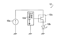
- the laser light source 12 has a light emitting layer interposed between a pair of reflecting layers by epitaxially growing a DC power source 12a and an AlGaAs-based or InGaAsP-based compound semiconductor on a substrate.
- a laser diode configured in a state, which outputs a laser beam having a constant wavelength ⁇ 1 in accordance with a drive current supplied from the DC power supply 12a, and a drive current supplied from the DC power supply 12a to the laser diode 12b
- a driver 12c made of a semiconductor switching element such as a transistor or FET, and a pulse generator 12d that outputs an opening / closing control signal for opening / closing the driver 12c at a predetermined frequency.
- 20 to 40 having a wavelength ⁇ 1
- a pulsed laser beam L having a pulse width of ns and a frequency of 27 to 98 kHz is output.
- the first optical coupler 18 and the second optical coupler 36 are similarly configured from a pair of optical waveguides made of, for example, optical fibers arranged close to each other.
- the first optical coupler 18 is connected to an optical fiber 38 at both ends to form a first waveguide 18 a that forms an annular closed propagation path of the optical waveguide 14, and both ends are optical.
- the second waveguide 18b connected to the fiber 30 and the optical fiber 31 is fixed in the main body 18c and brought close to each other for a predetermined distance so as to be optically coupled to each other at a predetermined ratio. In this case, the light is branched between the first waveguide 18a and the second waveguide 18b.
- the coupling coefficient is determined in accordance with the approach length between the first waveguide 18a and the second waveguide 18b ⁇ , the distance between them, and the like, and the first optical coupler 18 extracts, for example, at a rate of 1% (1:99).
- the coupling coefficient is set to 20 dB, and in the second optical coupler 36, the coupling coefficient is set so as to be extracted at a ratio of 50% (50:50).
- the optical waveguide 14 is configured by rotating an optical fiber 38 once or a plurality of times in a ring, and this optical fiber 38 is connected to the first waveguide 18 a of the first optical coupler 18. They are connected in series.
- the annular optical fiber 38 introduces the pulsed laser light L from the laser light source 12 supplied via the first optical coupler 18 through the optical fiber 38, so that the pulsed laser light L is transmitted through the same path.
- An annular closed-system propagation path for repeated propagation is formed.
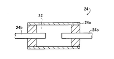
- the sample storage device 24 sandwiches the container 24 a interposed in the annular closed propagation path of the optical waveguide 14 in a state in which the sample 22 is stored, and the sample 22 in the container 24 a.
- a pair of optical fibers 24b whose end faces are opposed to each other, and an optical fiber 38 constituting a closed propagation path is connected in series to the pair of optical fibers 24b. Accordingly, the pulsed laser light L is repeatedly propagated through the sample 22 held in the container 24a in the annular closed propagation path of the optical waveguide 14.
- the sample storage device 24 is provided with a hole penetrating the core from the side surface in a part of the optical fiber 38 constituting the annular closed propagation path of the optical waveguide 14, and the sample 22 is filled in the hole. You may be comprised with what was made to do.
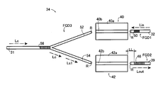
- the negative feedback amplification type semiconductor optical amplifier 34 corresponds to the intensity Iin of the first input light Lin.
- the light intensity amplification characteristic of the light other than the first wavelength ⁇ 1, that is, the first ambient light Ls1 having the first wavelength ⁇ 1 is modulated, and the light amplified from the first input light Lin and the intensity Iin of the first input light Lin.
- the first semiconductor optical amplifying element 40 that outputs light other than the first wavelength ⁇ 1 whose intensity has been inverted, that is, the first ambient light Ls1, and the light output from the first semiconductor optical amplifying element 40 are received.
- the light other than the first wavelength ⁇ 1 that is, the first ambient light Ls1 is separated by reflection, and the first ambient light Ls1 is transmitted via the optical fiber 31 to the control light Lc that is the second input light of the second wavelength ⁇ 2.
- a third optical fiber grating device FGD3 that is a wavelength selection element, and a combined light of the ambient light Ls1 from the third optical fiber grating device FGD3 and the control light Lc that is the second input light of the second wavelength ⁇ 2.
- the control light Lc ⁇ is modulated by the mutual gain modulation with the ambient light Ls1 of the first input light Lin and the amplified output light Lout and the light other than the second wavelength ⁇ 2 whose intensity is inverted with respect to the intensity Ic of the control light Lc That is, the second semiconductor optical amplifying element 42 that outputs the second ambient light Ls2 and the optical fiber 39 are provided.
- the second optical fiber grating that transmits the output light Lout having the second wavelength ⁇ 2 amplified by Lc but reflects the light other than the second wavelength ⁇ 2 of the light, that is, the second ambient light Ls2.
- a negative feedback amplification type three-terminal light having a second optical fiber grating device FGD2 that is an output optical fiber for re-inputting the reflected light to the second semiconductor optical amplification element 42.
- a signal amplifier fluorescent triode
- the second wavelength ⁇ 2 and the first wavelength ⁇ 1 are mutually included in the wavelength band of the surrounding light, or the second wavelength ⁇ 2 and the first wavelength ⁇ 1 are the same wavelength.
- the first wavelength ⁇ 1 is 1551 nm
- the second wavelength ⁇ 2 is set to a wavelength included in the wavelength band of the first ambient light Ls1 or the same wavelength 1551 nm. If the second wavelength ⁇ 2 of the control light Lc is 1549 nm, the wavelength of the output light Lout is 1549 nm. If the second wavelength ⁇ 2 of the control light Lc is 1551 nm, the wavelength of the output light Lout is 1551 nm.
- the first semiconductor optical amplifying element 40 and the second semiconductor optical amplifying element 42 are configured in the same manner from, for example, chip-shaped elements shown in FIG.
- the second semiconductor optical amplifying element 42 is composed of a semiconductor substrate 42a composed of a compound semiconductor, for example, indium phosphide InP, and a III-V group III mixed crystal semiconductor epitaxially grown thereon, and is formed with a predetermined width by photolithography.
- An optical waveguide 42b composed of a multilayer film having a relatively high refractive index, and a pn junction that constitutes a part of the multilayer film in the optical waveguide 42b, and includes a bulk, a multiple quantum well, a strained superlattice, and a quantum dot.
- the active layer 42c is composed of any of the above, an upper electrode 42e fixed to the upper surface of the optical waveguide 42b, and a lower electrode 42f fixed to the lower surface of the semiconductor substrate 42a.
- the first input light Lin having a predetermined wavelength ⁇ 1 is incident and is allowed to pass through the active layer 42c in the process of being propagated through the optical waveguide 42b.
- the light is amplified by the induced radiation action, it is output.
- first ambient light having a peripheral wavelength other than the wavelength ⁇ 1 centered on the wavelength ⁇ 1 and increasing or decreasing in inverse proportion to the intensity modulation of the first input light Lin (naturally generated) Light) ⁇ ⁇ Ls1
- second ambient light having an ambient wavelength other than the wavelength ⁇ 2 centered on the wavelength ⁇ 2 and the intensity increasing or decreasing inversely proportional to the intensity modulation of the control light (second input light) Lc (Light) ⁇ Ls2 is generated and output as well.
- the active layer 42c is composed of multiple wells, for example, it is composed of six pairs of InGaAs and InGaP of about 100 nm lattice-matched by epitaxial growth from the semiconductor substrate 42a, and on the active layer 42c, A guide layer (2000 ⁇ ) having a GRIN structure whose composition (refractive index) is changed in stages is sequentially provided.
- the device length of the active layer 42c is, for example, about 600 ⁇ m.
- a convex lens is provided between the input side end of the first semiconductor optical amplification element 40 of the optical fiber 32 and the second optical fiber grating device FGD2 provided at the end of the optical fiber 39 on the second semiconductor optical amplification element 42 side.
- a front spherical lens R functioning as an end face, between the optical fiber 32 and the input side end face of the first semiconductor optical amplifying element 40, and on the output side end face of the optical fiber 39 and the second semiconductor optical amplifying element 42.
- the signal light can be directly input or output.
- the distance between the output side end face of the semiconductor optical amplifying element 42 and the end face of the second optical fiber grating section 46, ie, the optical path length LL, is n for the refractive index of the optical transmission path between them and c (mm for the speed of light in vacuum. / Sec), and the time interval per pulse of the control light (second input light) Lc is t (sec), it is set to satisfy LL ⁇ (c ⁇ t) (20 ⁇ n). .
- the second semiconductor optical amplifying element 42 and the end of the second optical fiber grating device FGD2 and the end of the optical fiber 39 are supported by a bottom or wall of a case (not shown) after predetermined alignment. Accordingly, the positions are relatively fixed.
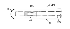
- the optical fiber 39 has a substantially cylindrical core 39a made of quartz SiO 2 doped with germanium Ge, and a substantially cylindrical shape having a refractive index lower than that of the core 39a and covering the outer peripheral surface thereof. And a cladding 39b made of quartz SiO 2 .
- the second optical fiber grating device FGD2 uses a phase mask or the like at the end of the core 39a, and periodically refracts typically about 10000 to 20000 layers due to a light-induced refractive index change caused by ultraviolet irradiation.
- the rate change includes a second optical fiber grating portion 46 formed in one or more groups in the propagation direction of the core 39a of the optical fiber.
- the refractive index change may have an equal period, but it may be one in which the period is sequentially changed in a chirp shape.
- the second optical fiber grating portion 46 functions as a second negative feedback amplification wavelength-selective reflecting element for generating a negative feedback amplification action in the second semiconductor optical amplification element 42, and the period of the refractive index thereof. And has a characteristic of selectively reflecting light having a wavelength corresponding to the effective refractive index, for example, transmits light of the second wavelength ⁇ 2 centered at 1551 nm, but is at least 3 nm or more different from the second wavelength ⁇ 2, for example 6 It functions as a wavelength selective filter that reflects light having a bandwidth of about 5 nm (second ambient light Ls2).
- FIG. 8 shows a spectrum of the amplified control light Lc (output light Lout) that is selectively passed by the second optical fiber grating unit 46, and FIG. 9 is selected by the second optical fiber grating unit 46.
- the spectrum of the second ambient light Ls2 that is reflected back is shown.
- the second ambient light Ls2 including the wavelength bands on both sides of the second wavelength ⁇ 2 is shown.
- the reflection characteristic of the second optical fiber grating portion 46 is that of the second ambient light Ls2. A part of them, for example, a wavelength band on one side of the first wavelength ⁇ 1 or a part thereof may be reflected.
- FIG. 9 shows a case where the second wavelength ⁇ 2 is 1551 nm, which is the same as the first wavelength ⁇ 1.
- the optical fiber 32 is also composed of a core and a clad made of quartz SiO 2 having a refractive index lower than that of the core and covering the outer peripheral surface of the core.
- a phase mask or the like is used, and a periodic refractive index change of typically about 10,000 to 20,000 layers due to a light-induced refractive index change caused by ultraviolet irradiation is a propagation direction of the core of the optical fiber.
- a first optical fiber grating device FGD1 including a first optical fiber grating portion 50 formed in one group or a plurality of groups is disposed.
- the first optical fiber grating section 50 functions as a first negative feedback amplification wavelength selective reflection element for generating a negative feedback amplification action in the first semiconductor optical amplification element 40. And has a characteristic of selectively reflecting light having a wavelength corresponding to the period of the refractive index and the effective refractive index. For example, light having a first wavelength ⁇ 1 centered at 1551 nm is transmitted. It functions as a wavelength selective filter that reflects light (first ambient light Ls1) having a wavelength of at least 3 nm or more different from the wavelength ⁇ 1 and having a bandwidth of, for example, about 6.5 nm.
- the distance between the input side end face of the first semiconductor optical amplifying element 40 and the end face of the first optical fiber grating section 50, that is, the optical path length LL, is defined as n for the refractive index of the transmission path between them and c for the speed of light in vacuum. mm / sec), and when the time interval per pulse of the first input light Lin is t (sec), LL ⁇ (c ⁇ t) (20 ⁇ n) is set to be satisfied.
- a predetermined alignment is applied between the first semiconductor optical amplification element 40 and the end of the first optical fiber grating device FGD1 and the end of the optical fiber 39, and then supported by the bottom or wall of a case (not shown). Accordingly, the positions are relatively fixed.
- the first optical fiber grating section 50 and the second optical fiber grating section 46 cause the first ambient light Ls1 in the surrounding wavelength band of the first wavelength ⁇ 1 and the second ambient light Ls2 in the surrounding wavelength band of the second wavelength ⁇ 2 to be the first semiconductor.
- a negative feedback amplification action is generated, so that a stable output can be obtained with little noise, a high degree of modulation.
- the second semiconductor optical amplifying element 42 for example, the control light (second input light) Lc and the first ambient light Ls1 having the first wavelength ⁇ 1 shown in FIG.
- the second semiconductor optical amplifying element 42 amplifies the control light Lc of the first wavelength ⁇ 1, and generates second ambient light Ls2 other than the wavelength ⁇ 1 whose intensity is inverted. And the combined light is output.
- These lights are output to the second optical fiber grating device FGD2.
- the second optical fiber grating section 46 provided therein provides the first wavelength ⁇ 1 that is the amplified light of the control light Lc of the above light.
- FIG. 11 shows the reflected light of the second optical fiber grating section 46 that changes in synchronization with the control light Lc having the first wavelength ⁇ 1 shown in FIG. 10 inputted to the second semiconductor optical amplifying element 42, that is, the second semiconductor.
- the second ambient light Ls2 re-input to the optical amplifying element 42 is shown.
- FIG. 12 shows the output light Lout output from the second optical fiber grating device FGD2 in a dotted line when the second ambient light Ls2 that is the negative feedback light is not input to the second semiconductor optical amplifier 42 in the experiment.
- the solid line represents the output light Lout output from the second optical fiber grating device FGD2 when negative feedback light (second ambient light Ls2) is input to the second semiconductor optical amplifier 42.
- the waveform of the output light (signal light) Lout output from the second optical fiber grating device FGD2 is not distorted, and nonlinear distortion is reduced.
- the negative feedback effect in the optical amplification is obtained by inputting the negative feedback light (second ambient light Ls2), so that the gain is stabilized and nonlinear distortion is reduced. Further, since the minimum value (base line of the signal) of the output light output from the second optical fiber grating device FGD2 is set to a value lower than that indicated by the dotted line, the negative feedback light (second ambient light Ls2) Is input, thereby obtaining a negative feedback effect in optical amplification, thereby increasing the degree of modulation of the output light Lout to be output and reducing the noise to increase the S / N ratio.
- FIG. 13 shows the output light Lout output from the second optical fiber grating device FGD2 when the second ambient light Ls2 as negative feedback light is input to the second semiconductor optical amplifying element 42 in the above experiment.
- FIG. 14 shows the result of pattern measurement (the pattern displayed on the oscilloscope).
- FIG. 14 shows the second optical fiber grating when the negative feedback light (the second ambient light Ls2) is not input to the second semiconductor optical amplifier 42 in the above experiment.
- the result (eye pattern displayed on the oscilloscope) of the output light Lout ⁇ output from the device FGD2 is shown.
- a test pattern PEBS31, a mark ratio of 1/2, and a standard mask SYM16 / OC48 (2.48832 GHz) were used for the eye pattern measurement.
- FIG. 13 when negative feedback light (second ambient light Ls2) is input to the second semiconductor optical amplifying element 42, the signal of the output light Lout output from the second optical fiber grating device FGD2 is It has been greatly stabilized.
- the third fiber grating device FGD3 is provided in the two optical fibers 52 and 54 connected to the optical fiber 31 and the melt-stretched portion where the end portions on the optical fiber 31 side are melt-stretched.
- the third optical fiber grating unit 56 is configured to transmit the amplified light of the first input light Lin having the first wavelength ⁇ 1 out of the output light of the first semiconductor optical amplifier element 40 input to the optical fiber 52.
- the first ambient light Ls1 that is light having a wavelength other than the one wavelength ⁇ 1 is reflected and input from the optical fiber 54 to the second semiconductor optical amplifier 42.
- the third fiber grating device FGD3 transmits part of the pulsed laser light L transmitted through the optical fiber 31 and propagating through the optical waveguide 14 extracted from the first optical coupler 18, Two-input light, that is, control light Ic is input to the second semiconductor optical amplifying element 42. That is, the third fiber grating device FGD3 functions as a wavelength selection element, receives the output light of the first semiconductor optical amplification element 40, and outputs the first ambient light Ls1 that is light other than the first wavelength of the output light. While being separated by reflection, the first ambient light Ls1 is combined with the control light LcL that is the second input light having the second wavelength ⁇ 2 through the optical fiber 31, and is output to the second semiconductor optical amplifying element 42.
- the end surfaces of the two optical fibers 52 and 54 are each provided with a tip lens R that functions as a convex lens, and the output light of the first semiconductor optical amplification element 40 is directly input to the optical fiber 52 from the end surfaces.
- the light output from the optical fiber 54 is directly input to the end face of the second semiconductor optical amplifying element 42. That is, between the end face of the optical fiber 52 and the end face of the first semiconductor optical amplifying element 40, and also between the end face of the second semiconductor optical amplifying element 42 and the optical fiber 54, directly without using other optical components. Are combined.
- the melt drawing portion of the third fiber grating device FGD3 constitutes a so-called fiber type coupler in which the cores are mutually melted and stretched over a predetermined length to branch into a Y type, and the third fiber grating device FGD3 has its melting point.
- a phase mask or the like is used, and a periodicity of typically about 10,000 to 20,000 layers due to a light-induced refractive index change due to ultraviolet irradiation.
- the third optical fiber grating portion 56 in which the refractive index change is formed in one group or a plurality of groups in the propagation direction of the core, light of the first wavelength ⁇ 1 is transmitted, but other than the first wavelength ⁇ 1.
- the light, that is, the first ambient light Ls1 not including the first wavelength ⁇ 1 is reflected.
- the output light Lout is not simply amplified from the first input light Lin having the first wavelength ⁇ 1, but the control light (second input light) Lc.
- the second ambient light Ls2 is modulated and amplified, and the output light Lout ⁇ of the second wavelength ⁇ 2 is transmitted through the second optical fiber grating portion 46, and at the same time other than the second wavelength ⁇ 2.
- the second ambient light Ls2 indicating intensity inversion is fed back to control the gain of the second semiconductor optical amplification element 42 (
- the second input light) is modulated according to Lc to obtain a negative feedback light amplification effect, the output light Lout is effectively reduced in distortion of the signal waveform, and a high modulation degree is obtained with low noise, resulting in an error rate. (Bit error) is about 2 digits The effect of lowering is obtained.
- a small three-terminal optical signal amplifier (fluorescent triode) ⁇ ⁇ that outputs the output light Lout ⁇ having the first wavelength ⁇ 1 modulated by the control light can be obtained.
- the arithmetic unit 26 is composed of a so-called microcomputer, which processes the output light Lout of the negative feedback amplification type semiconductor optical amplifier 34 detected by the photodetector 20 in accordance with a program stored in advance, and uses ring-down spectroscopy. Thus, the component of the sample 22 is specified.
- the arithmetic unit 26 calculates the attenuation waveform of the pulse group obtained from the photodetector 20 when the pulsed laser light L is output when the sample 22 is not yet accommodated in the sample accommodating device 24, and
- the ring-down time ⁇ 0 is obtained in advance from the attenuation waveform, and then the pulse group obtained from the photodetector 20 when the pulsed laser beam L is output when the sample 22 is not yet accommodated in the sample accommodating device 24.
- the ring-down time ⁇ is calculated from the attenuation waveform. For example, the number of samples 22 is calculated based on the actual ring-down times ⁇ 0 and ⁇ from the relationship stored in advance in the equation (4).
- the sample 22 is specified by calculating the density n.
- a part of the pulsed laser light L circulated in the optical fiber 38 constituting the annular closed propagation path in the optical waveguide 14 is transmitted from the first optical coupler 18 at a predetermined ratio, for example, 1/100 each time it circulates. Therefore, every time the pulsed laser beam L is output, the attenuated waveform of the extracted light, that is, the pulse group is observed as shown in FIG. 15, for example. This waveform is attenuated as time elapses, and the attenuation rate changes according to the material state of the sample 22 through which a part of the circulated first input light L is transmitted.
- the waveform is represented by the time function I (t) of the following equation (1), where the initial intensity is I 0 .
- I (t) I 0 exp ⁇ (1 / ⁇ 0 ) t (1)
- (1 / ⁇ 0 ) is an attenuation rate.
- ⁇ 0 is a time until the intensity becomes 1 / e, that is, a time constant, and is also referred to as a reference ring down time.
- Equation (1) can be rewritten as Equation (3).
- Equation (4) is obtained from Equation (2).
- I (t) I 0 exp ⁇ (t / ⁇ 0 ⁇ nct) (3)
- n 1 / ⁇ c (1 / ⁇ 1 / ⁇ 0 ) (4)
- the absorbance analyzer 10 of the present embodiment configured as described above, a part of the pulsed first laser L that is circulated in the optical fiber 38 that forms the annular closed propagation path in the optical waveguide 14 is obtained.
- the control light Lc is extracted from the first optical coupler 18 at a predetermined rate, for example, 1/100, and the first input light Lin is modulated by the negative feedback amplification type semiconductor optical amplifier 34.
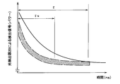
- the signal intensity (power) detected by the photodetector 20 with the negatively amplified output light Lout ⁇ is observed with an oscilloscope, an attenuation waveform as shown by the solid line in FIG. 16 is obtained.
- the frequency characteristic of the oscilloscope is not sufficiently high, so it is not displayed in a pulse shape as shown in FIG. 15, but an envelope of those pulses is displayed.
- the arithmetic unit 26 measures the ring-down time ⁇ by measuring the time between the initial value time point of the attenuation curve indicated by the solid line and the time point that is 1 / e of the initial value, and (4) The number density n of the sample 22 is calculated and displayed on the display device 28.
- a thick attenuation curve indicated by a one-dot chain line in FIG. 16 indicates an attenuation waveform detected by the photodetector 20 when the negative feedback amplification type semiconductor optical amplifier 34 is not used.
- the S / N is low and unstable, and the ring-down time ⁇ N is significantly short, so that the measurement accuracy as high as that of the present embodiment cannot be obtained.
- the negative feedback amplification type semiconductor optical amplifier 34 is provided between the first optical coupler 18 and the photodetector 20, and the negative feedback amplification type semiconductor light is provided.
- the amplifier 34 receives a part of the pulsed laser light L having the wavelength ⁇ 1 branched by the second optical coupler 36 as the first input light Lin and repeats the inside of the optical waveguide 14 taken out from the first optical coupler 18.
- the propagating pulsed laser light L As control light (second input light) Lc and negatively amplifying the first input light Lin, it has the same wavelength ⁇ 2 as the control light Lc,
- the output light Lout that is intensity-modulated by the first ambient light Ls1 of the first input light Lin is output to the photodetector 20
- the light (signal) that is detected by the photodetector 20 is obtained by negative feedback amplification. S / N ratio with less waveform distortion It becomes elevated. For this reason, there is no oscillation in the closed propagation path of the optical waveguide 14, and stable absorption analysis is possible.
- the S / N ratio of the observed waveform in which the light intensity of the pulsed laser beam L decays with time is high and the noise contained in the waveform is reduced, the signal of the pulsed laser beam L from such a signal is reduced. Since the time until the light intensity is attenuated, that is, the ring-down time ⁇ is long and accurately obtained, the measurement accuracy for the attenuation of the attenuation curve can be sufficiently obtained.
- the negative feedback amplification type semiconductor optical amplifier 34 amplifies and outputs the first input light Lin that is a part of the pulsed laser light L having the predetermined wavelength ⁇ 1.
- a first semiconductor optical amplifying element 40 that emits first ambient light Ls1 other than the wavelength ⁇ 1 ⁇ of the pulsed laser light L whose intensity is inverted with respect to the intensity of the pulsed laser light L, and the first semiconductor optical amplifying element
- the second ambient light Ls2 having a wavelength different from the wavelength ⁇ 2 of Lc is reflected by the second optical fiber grating portion 46 and is incident again on the second semiconductor optical amplifying element 42 to generate a negative feedback amplification action. So light Light detected in can 20 (signal) becomes the S / N ratio is enhanced by the negative feedback amplifier.
- the second optical fiber grating section (second negative feedback amplification wavelength selective reflection element) 46 is optically connected to the output side of the second semiconductor optical amplification device 42.
- the second negative feedback amplification wavelength-selective reflecting element 46 is provided in the end of the output side optical fiber 39 and is reduced in size because it is configured to be incident, the absorption spectrometer 10 is reduced in size.
- the front lens R is disposed on the end surface of the output side optical fiber 39 on the side of the second semiconductor optical amplification element 42 provided with the second optical fiber grating portion 46. Since the output side optical fiber 39 and the second semiconductor optical amplifying element 42 are directly optically coupled via the front ball lens R, an optical element such as a lens for optical coupling is provided. Since no parts are required, the coupling structure is simple and small, and the absorbance analyzer 10 is miniaturized.
- the second optical fiber grating unit 46 transmits light having the wavelength ⁇ 2 of the output light Lout and is at least 3 nm or more generated by amplification of the second semiconductor optical amplification element 42.
- a second semiconductor optical amplifier having a reflection characteristic that reflects all or a part of light in a shorter wavelength side and / or longer wavelength side than the wavelength of the output light Lout Since the element 42 is disposed close to the element 42 with a predetermined optical path length LL, the absorption spectrometer is further downsized.
- the predetermined optical path length LL is expressed by the refractive index of the optical transmission path between the second semiconductor optical amplifying element 42 and the second optical fiber grating section 46 being n, LL ⁇ (c ⁇ t) / (20 ⁇ n) where c (mm / sec) is the speed of light in vacuum and t (seconds) is the time interval between pulses of control light Lc (output light Lout).
- c (mm / sec) is the speed of light in vacuum
- t (seconds) is the time interval between pulses of control light Lc (output light Lout).
- the negative feedback amplification type semiconductor optical amplifier 34 is provided on the input side of the first semiconductor optical amplification element 40 and is input to the first semiconductor optical amplification element 40.
- the first input light Lin is allowed to pass, but all or part of the first ambient light Ls1 emitted from the first semiconductor optical amplifier element 40 to the input side is reflected and re-input to the first semiconductor optical amplifier element 40. Since the first optical fiber grating section 50 (first negative feedback amplification wavelength-selective reflection element) to be included is included, the first semiconductor optical amplification element 40 can also obtain a negative feedback action, and the waveform distortion is further reduced. The S / N ratio is increased.
- the first optical fiber grating section 50 (first negative feedback amplification wavelength selective reflection element) is optically connected to the input side of the first semiconductor optical amplification element 40.
- the first semiconductor optical amplification is provided by reflecting all or part of the first ambient light Ls1 provided at the end of the coupled input optical fiber 32 and emitted from the first semiconductor optical amplification element 40 to the input side. Since the first optical fiber grating section 50 is provided in the end portion of the input side optical fiber 32 and is reduced in size because the light is incident on the element 40 again, the absorption spectrometer 10 is reduced in size.
- the front lens R is disposed on the end surface of the input side optical fiber 32 provided with the first optical fiber grating section 50 on the first semiconductor optical amplification element 40 side. Since the optical fiber 32 and the first semiconductor optical amplifying element 40 are directly optically coupled via the tip lens R, a lens for optical coupling is provided. Since no components are required, the coupling structure is further simplified and reduced in size, and the absorption spectrometer 10 is reduced in size.
- the first optical fiber grating section 50 transmits the light having the first wavelength ⁇ 1 of the first input light Lin, and is generated by amplification of the first semiconductor optical amplifier element 40. Further, with respect to the amplified light in a band of at least 3 nm or more, it has a reflection characteristic of reflecting all or a part of the light on the shorter wavelength side and / or the longer wavelength side than the wavelength ⁇ 1 of the first input light Lin, In addition, since the first semiconductor optical amplifying element 40 is disposed in close proximity with a predetermined optical path length LL, the absorption spectrometer 10 is further downsized.
- the predetermined optical path length LL is such that the refractive index of the optical transmission path between the first semiconductor optical amplification element 40 and the first optical fiber grating section 50 is n, and the vacuum Since the speed of light in the medium is c (mm / sec) and the time interval of the pulses of the first input light Lin is t (seconds), LL ⁇ (c ⁇ t) / (20 ⁇ n). 1 High responsiveness of the semiconductor optical amplifying element 40 can be obtained. Therefore, since the first ambient light Ls1 reflected by the first optical fiber grating unit 50 is quickly re-input to the first semiconductor optical amplifying element 40 without delay, distortion of the signal waveform is effectively reduced, and A high degree of modulation can be obtained.
- the negative feedback amplification type semiconductor optical amplifier 34 described above may be as follows.
- the input position of the control light Lc ⁇ ⁇ ⁇ is changed in the third fiber grating device FGD3 as compared with the negative feedback amplification type semiconductor optical amplifier 34 of the first embodiment.
- the others are similarly configured.
- a branched optical fiber 62 branched from the optical fiber 54 is provided among the two optical fibers 52 and 54 provided in the melt-stretched portion whose one end is melt-stretched. It has been.
- a Y-shaped branch is formed by forming a melt-stretched portion of the core. The same function is obtained by inputting the control light Lc from the branch optical fiber 62. Therefore, according to the absorption spectrometer 10 provided with the negative feedback amplification type semiconductor optical amplifier 60, the same effect as that of the above-described embodiment can be obtained.
- a negative feedback amplification type semiconductor optical amplifier 64 shown in FIG. 18 has the same function as that of the negative feedback amplification type semiconductor optical amplifier 34 of the first embodiment. However, instead of the third optical fiber grating device FGD3, an adder is used.
- the drop filter 66 is provided, the first input optical fiber 68 provided in the add / drop filter 66 and the first semiconductor optical amplifying element 40, and the output optical fiber 72 provided in the add / drop filter 66.
- the second semiconductor optical amplifying element 42 is directly coupled to the first input optical fiber 68 and the front spherical lens R functioning as a convex lens formed on the distal end surfaces of the output optical fiber 72. And the second semiconductor optical amplifying element 42 and the first semiconductor optical amplifying element 40 are different from each other in that they are composed of one common chip.
- the add / drop filter 64 has a first input optical fiber 68 to which the output of the first semiconductor optical amplifier element 40 is input, a second input optical fiber 70 to which the control light Lc is input, and a second semiconductor optical amplifier element. And an output optical fiber 72 for output to 42.
- the add / drop filter 66 reflects the first ambient light Ls1 other than the second wavelength ⁇ 1 of the light input from the first input optical fiber 68 to the output optical fiber 72, and the control light input from the second input optical fiber 70. Lc is transmitted to the output optical fiber 72. Therefore, according to the negative feedback amplification type semiconductor optical amplifier 64 of the present embodiment, the same effect as that of the first embodiment can be obtained.
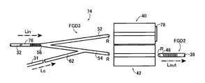
- the negative feedback amplification type semiconductor optical amplifier 74 shown in FIG. 19 has the same function as that of the negative feedback amplification type semiconductor optical amplifier 60 of the second embodiment shown in FIG. The difference is that the third optical fiber grating device FGD3 is also connected to the optical fiber 32 and used as four terminals.
- the first semiconductor optical amplifying element 40 functions as a reflective semiconductor optical amplifier having characteristics such as a high degree of modulation by being provided with the reflective film 78.
- the third optical fiber grating device FGD3 of the present embodiment includes a third optical fiber grating portion 56 provided in a melt-stretched portion in which ends of the two optical fibers 52 and 54 are melt-stretched, and a first wavelength ⁇ 1. And a third input unit 76 connected to the optical fiber 32 so as to receive the first input light Lin.
- the first input light Lin having the first wavelength ⁇ 1 is input to the third input unit 76 of the third optical fiber grating device FGD3, the first input light Lin is the third light.
- the light passes through the fiber grating portion 56 and enters the first semiconductor optical amplification element 40.
- the first semiconductor optical amplifying element 40 the first input light Lin having the first wavelength ⁇ 1 is amplified and the first ambient light Ls1 not including the first wavelength ⁇ 1 whose intensity phase is inverted is generated.
- the first ambient light Ls1 is output to both sides, but the first ambient light Ls1 directed toward the reflective film 78 is reflected by the reflective film 78 and is incident on the optical fiber 52 of the third optical fiber grating device FGD3.
- the third optical fiber grating unit 56 reflects the first ambient light Ls1 other than the first wavelength ⁇ 1 out of the light input from the optical fiber 52 to the optical fiber 54, and functions as the second input light from the branch fiber 62.
- the control light Lc having the second wavelength ⁇ 2 is input and combined.
- the first ambient light Ls1 other than the combined first wavelength ⁇ 1 and the control light Lc having the second wavelength ⁇ 2 are input to the second semiconductor optical amplifier 42. Therefore, according to the negative feedback amplification type semiconductor optical amplifier 74 of the present embodiment, in addition to the same effects as the negative feedback amplification type semiconductor optical amplifier 60 of the second embodiment shown in FIG. Since the optical amplifying element 40 is a reflective semiconductor optical amplifier, there is an advantage that the degree of modulation and the S / N ratio can be further increased.
- the negative feedback amplification type semiconductor optical amplifier 80 of the embodiment shown in FIG. 20 is different from the negative feedback amplification type semiconductor optical amplifier 74 in place of the reflection film 78 fixed to the end face of the first semiconductor optical amplification element 40.
- the input side optical fiber 32 provided with the first optical fiber grating section 50 of FIG. 5 is provided, and the second semiconductor optical amplifying element 42 and the first semiconductor optical amplifying element 40 are configured from a common one chip. The other points are the same, and the others are similarly configured.
- the first ambient light Ls1 generated in the first semiconductor optical amplifying element 40 is output to both sides, but the first ambient light Ls1 directed to the input side optical fiber 32 is the first optical fiber.
- the first input light Lin may be input from the input-side optical fiber 32 or may be input from the third input unit 76 of the third optical fiber grating device FGD3.
- the input-side optical fiber 32 provided with the first optical fiber grating section 50 functions as a means for reflecting the first ambient light Ls1.
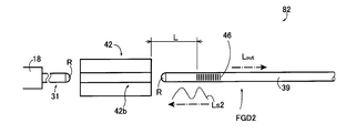
- the negative feedback amplification type semiconductor optical amplifier 82 of the embodiment shown in FIG. 21 is different from the negative feedback amplification type semiconductor optical amplifiers 34, 60, 74, 80 in that the first semiconductor optical amplification element 40, the first optical fiber grating.
- the first and second optical fiber grating portions 56 and 56 are removed, and the second semiconductor optical amplification element 42 and the second optical fiber grating portion 46 are different from each other.
- the control light Lc having the first wavelength ⁇ 1 is amplified in the second semiconductor optical amplifying element 42
- the second ambient light Ls2 having the surrounding wavelength of the wavelength ⁇ 1 of the control light Lc is converted into the second optical fiber grating section.
- the stable output light Lout with a high S / N ratio obtained by amplifying the control light Lc is the second optical fiber grating. Since the light is output through the unit 46, as in the above-described embodiment, there is no oscillation in the closed propagation path of the optical waveguide 14, and stable absorption analysis is possible. In addition, since the S / N ratio of the observed waveform in which the light intensity of the pulsed laser beam L decays with time is high and the noise contained in the waveform is reduced, the signal of the pulsed laser beam L from such a signal is reduced.
- the negative feedback amplification type semiconductor optical amplifier 82 does not include the first semiconductor optical amplification element 40, the first optical fiber grating unit 50, and the third optical fiber grating unit 56, and Since the optical fiber 32 and the second optical coupler 36 are not required in the absorption spectrometer 10, there is an advantage that the absorption analyzer 10 can be configured more easily.
- an optical signal amplifier for amplifying an optical signal composed of, for example, an EDFA, and a filter for removing noise are provided as necessary at a position indicated by a dashed square, for example. Can be provided.
- the first optical coupler 18 introduces a part of the pulsed laser light L into the optical waveguide 14 at a predetermined ratio, and also circulates in the optical waveguide 14.
- a part of the laser beam L is derived at a predetermined ratio, it may be divided into two parts for introduction and for introduction.
- the optical waveguide 14 has an annular closed-system propagation path composed of an optical fiber 38 wound in an annular shape.
- the optical waveguide 14 may have a closed propagation path configured to reciprocate along the same path.
- a part of the pulsed laser light L that reciprocates in the closed propagation path can be derived at a rate of 1% (1:99). .
- the configuration of the negative feedback amplification type semiconductor optical amplifier 34, 60, 64, 74, 80, 82 described above may be variously changed as necessary.
- the light absorption rate ⁇ k of the sample 22 may be calculated from the measured attenuation rate k.
- the first optical fiber grating section 50 for causing the first semiconductor optical amplification element 40 to perform negative feedback amplification is not necessarily provided. May be. It is sufficient that at least the second semiconductor optical amplifying element 42 performs negative feedback amplification.
- Optical waveguide 18 First optical coupler (optical coupler device) 20: photodetector 22: sample 24: sample storage device 32: input side optical fibers 34, 60, 64, 74, 80: negative feedback amplification type semiconductor optical amplifier 39: output side optical fiber 40: first semiconductor optical amplification element 42: second semiconductor optical amplifier 46: second optical fiber grating section (second negative feedback amplification wavelength selective reflection element) 50: 1st optical fiber grating part (the 1st wavelength selective reflection element for negative feedback amplification) 56: Third optical fiber grating (first wavelength selection element) Lin: first input light Lc: control light (second input light) Lout: output light LL: optical path length R: tip ball lens
Landscapes
- Physics & Mathematics (AREA)
- Spectroscopy & Molecular Physics (AREA)
- Analytical Chemistry (AREA)
- Health & Medical Sciences (AREA)
- Life Sciences & Earth Sciences (AREA)
- Chemical & Material Sciences (AREA)
- Optics & Photonics (AREA)
- Biochemistry (AREA)
- General Health & Medical Sciences (AREA)
- General Physics & Mathematics (AREA)
- Immunology (AREA)
- Pathology (AREA)
- Investigating Or Analysing Materials By Optical Means (AREA)
- Optical Modulation, Optical Deflection, Nonlinear Optics, Optical Demodulation, Optical Logic Elements (AREA)
Abstract
高い測定精度で安定して測定できる吸光分析装置を提供する。 第1光カプラ18と光検出器20との間に負帰還増幅型半導体光増幅器34が備えられ、その負帰還増幅型半導体光増幅器34は、第1入力光Linを負帰還増幅することにより、制御光Lc と同じ波長λ2を有し、且つ第1入力光Linの第1周囲光Ls1により強度変調された出力光Lout を光検出器20へ出力することから、その光検出器20に検出される光( 信号) は、負帰還増幅によって波形の歪みが少なくS/N比が高められたものとなる。光導波器14の閉鎖系伝播経路内での発振がなく、安定した吸光分析が可能となる。パルス状レーザ光Lの光強度が時間経過に伴って減衰する減衰波形のS/N比が高くその波形に含まれるノイズが少なくなることから、減衰曲線の減衰に対する測定精度が十分に得られる。
Description
本発明は、負帰還増幅機能を有する半導体光増幅器を用いた吸光分析装置に関するものである。
光透過性を有する物質の吸光特性を利用して試料を分析する装置として、所謂キャビティリングダウン法を用いた光分析装置が知られている。この光分析装置では、閉鎖系に構成された伝播経路内にたとえば数十kHz程度の周波数のパルス状であって所定波長のレーザ光を環状の伝播経路内に周回させ或いはミラー間に設けられた直線状の伝播経路内で往復させ、試料を充填したセルをその閉鎖系伝播経路に介挿したとき、その光伝播経路内を伝播するパルス状レーザ光の強度が時間経過に伴って減衰する減衰波形が光検出器を用いて検出され、その減衰波形のリングダウンタイム或いは減衰率が求められ、予め設定された関係からそのリングダウンタイム或いは減衰率に基づいて試料の数密度或いは吸光率が測定される。この試料の数密度或いは吸光率に基づいて、試料中に含まれる物質を特定したり、その物質の定量をしたりすることが行われるようになっている。たとえば、特許文献1、特許文献2に記載された吸光分析装置がそれである。
ところで、上記パルス状レーザ光の光強度の減衰率を測定するに際しては、光検出器を用いて観測される、そのパルス状レーザ光の光強度が時間経過に伴って減衰する減衰波形にノイズが混入し易く、S/N比が低い。このため、そのような減衰波形信号からパルス状レーザ光の光強度が1/eまで減衰するまでの時間であるリングダウンタイムが短くしかも正確に得られないし、或いは、減衰率も同様に正確に得られないので、測定精度が十分に得られなかった。
これに対して、上記特許文献2の段落0033に記載されているように、閉鎖系伝播経路内或いは外に光増幅器を介挿することによりその光伝播経路内を伝播するレーザ光の強度を高めて、光検出器により検出される信号の強度を高めることが提案されている。しかしながら、このような構成によれば、ノイズも増幅されることから信号のS/N比が十分に改善されず、しかも上記閉鎖系伝播経路内でレーザ光が発振し易く、測定が不能となるか或いは不安定となる場合もあった。
本発明は以上の事情を背景としてなされたものであり、その目的とするところは、高い測定精度で安定して測定できる吸光分析装置を提供することにある。
本発明者等は、以上の事情を背景として種々検討を重ねた結果、光検出器により検出される光、すなわち前記閉鎖系伝播経路内から取り出された光伝播経路内の光の一部を負帰還増幅機能を有する光増幅器を用いて増幅すると、S/N比が高く改善されると同時に、上記閉鎖系伝播経路内での発振がなく、高精度で安定した吸光分析が可能となるという事実を見いだした。本発明は係る知見に基づいて為されたものである。
すなわち、前記目的を達成するための請求項1にかかる発明は、(a) 所定波長のパルス状レーザ光を出力するレーザ光源と、(b) 周回または往復させることによって光を繰り返し伝播させる閉鎖系伝播経路を有する光導波器と、(c) その光導波器の閉鎖系伝播経路に設けられ、前記レーザ光源とその光導波器とを光学的に結合してそのレーザ光源から出力されるパルス状レーザ光をその光導波器の閉鎖系伝播経路内に入力し、且つその閉鎖系伝播経路内を繰り返し伝播するパルス状レーザ光の一部を取り出す光カプラ装置と、(d) その光カプラ装置により前記光導波器の閉鎖系伝播経路内から取り出された前記パルス状レーザ光の一部を検出する光検出器と、(e) 試料を収容した状態で前記光導波器の閉鎖系伝播経路に設けられ、その光導波器の閉鎖系伝播経路内においてその試料を通して前記パルス状レーザ光を繰り返し伝播させる試料収容装置とを備え、前記光検出器により検出される前記パルス状レーザ光の一部の強度の減衰率に基づいて前記試料を分析する吸光分析装置であって、(f) 前記光カプラ装置から取り出された前記光導波器内を伝播するパルス状レーザ光の一部を入力光として受けて、該入力光が負帰還増幅された出力光を前記光検出器へ出力する負帰還増幅型半導体光増幅器を、前記光カプラ装置と前記光検出器との間に備えることを特徴とする。
請求項1に係る発明の吸光分析装置によれば、前記光カプラ装置と前記光検出器との間に負帰還増幅型半導体光増幅器が備えられ、その負帰還増幅型半導体光増幅器は、前記光カプラ装置から取り出された前記光導波器内を伝播するパルス状レーザ光の一部を入力光として受けて、該入力光が負帰還増幅された出力光を前記光検出器へ出力することから、その光検出器に検出される光は、負帰還増幅によって波形の歪みが少なくS/N比が高められたものとなる。このため、上記閉鎖系伝播経路内での発振がなく、安定した吸光分析が可能となる。しかも、パルス状レーザ光の光強度が時間経過に伴って減衰する観測波形のS/N比が高くその波形に含まれるノイズが少なくなることから、そのような信号からパルス状レーザ光の光強度が減衰するまでの時間すなわちリングダウンタイムが長くしかも正確に得られるようになるので、減衰曲線の減衰に対する測定精度が十分に得られる。
ここで、好適には、前記吸光分析装置において、前記負帰還増幅型半導体光増幅器は、前記光カプラ装置により取り出されたパルス状レーザ光の一部を第1入力光として受けるとともに、前記光カプラ装置から取り出された前記光導波器内を伝播する前記パルス状レーザ光の一部を第2入力光として受けて、負帰還増幅することにより、該第2入力光と同じ波長を有し、且つ該第1入力光の周囲光により強度変調された出力光を前記光検出器へ出力するものである。このようにすれば、光検出器に検出される光は、負帰還増幅によって波形の歪みが少なくS/N比が高められたものとなるので、上記閉鎖系伝播経路内での発振がなく、安定した吸光分析が可能となる。しかも、パルス状レーザ光の光強度が時間経過に伴って減衰する観測波形のS/N比が高くその波形に含まれるノイズが少なくなることから、そのような信号からパルス状レーザ光の光強度が減衰するまでの時間すなわちリングダウンタイムが長くしかも正確に得られるようになるので、減衰曲線の減衰に対する測定精度が十分に得られる。
また、好適には、前記吸光分析装置において、前記負帰還増幅型半導体光増幅器は、前記所定波長のパルス状レーザ光の一部である前記第1入力光を増幅して出力すると共に、そのパルス状レーザ光の強度に対して強度反転したそのパルス状レーザ光の波長以外の第1周囲光を放射する第1半導体光増幅素子と、その第1半導体光増幅素子から出力される光から前記第1周囲光の全部または一部を選択する第1波長選択素子と、その第1波長選択素子により選択された前記第1周囲光の全部または一部と、前記光カプラ装置により前記光導波器の閉鎖系伝播経路から取り出されたパルス状レーザ光の一部である第2入力光とが入力され、その第2入力光の波長を有し、且つその第1入力光の周囲光により強度変調された出力光を出力する第2半導体光増幅素子と、前記第2半導体光増幅素子から出力側へ放射される光のうち、前記第2入力光の波長の光を透過させるが、その第2入力光の波長とは異なる波長に光を反射してその第2半導体光増幅素子へ入射させる第2負帰還増幅用波長選択性反射素子とを、含む。このようにすれば、第2半導体光増幅素子から出力側へ放射される光のうちその第2入力光の波長とは異なる波長に光が第2負帰還増幅用波長選択性反射素子により反射されることによりその第2半導体光増幅素子へ再び入射させられて負帰還増幅作用が発生させられるので、前記光検出器に検出される光( 信号光) は、負帰還増幅によってS/N比が高められたものとなる。
また、好適には、前記吸光分析装置において、前記第2負帰還増幅用波長選択性反射素子は、前記第2半導体光増幅素子の出力側に光学的に結合された出力側光ファイバの端部に設けられ、その第2半導体光増幅素子から放出される第2周囲光の全部または一部を反射してその第2半導体光増幅素子へ再入射させる第2光ファイバグレーティング部である。このようにすれば、第2負帰還増幅用波長選択性反射素子が出力側光ファイバの端部内に設けられて小型化されるので、吸光分析装置が小型化される。
また、好適には、前記吸光分析装置において、出力側光ファイバの前記第2光ファイバグレーティング部が設けられた前記第2半導体光増幅素子側の端部の端面には先球レンズが備えられ、その出力側光ファイバとその第2半導体光増幅素子との間は、その先球レンズを介して直接的に光学結合される。このようにすれば、光学結合の為のレンズなどの光学部品を必要としないので、結合構造が簡単且つ小型となり、吸光分析装置が小型化される。
また、好適には、前記吸光分析装置において、前記第2光ファイバグレーティング部は、前記出力光の波長の光を透過させ、前記第2半導体光増幅素子の増幅により生じた少なくとも3nm以上の帯域の増幅光に対して、前記出力光の波長よりも短波長側および/または長波長側の帯域の全部または一部の光を反射する反射特性を有し、かつ、前記第2半導体光増幅素子に対して所定の光路長LLを隔てて近接して配置される。このようにすれば、吸光分析装置が小型化される。
また、好適には、前記吸光分析装置において、前記所定の光路長LLは、前記第2半導体光増幅素子と第1光ファイバグレーティング部との間の光伝送路の屈折率をn、真空中の光速をc(mm/秒)、前記第2入力光のパルスの時間間隔をt(秒)としたとき、LL≦(c・t)/(20・n)である。このようにすれば、第2半導体光増幅素子の高い応答性が得られる。したがって、第1光ファイバグレーティング部により反射された第2周囲光が第2半導体光増幅素子へ遅れなく速やかに再入力されるので、効果的に信号波形の歪みが低減されるとともに、高い変調度が得られる。
また、好適には、前記吸光分析装置において、前記負帰還増幅型半導体光増幅器は、前記第1半導体光増幅素子の入力側に設けられ、その第1半導体光増幅素子へ入力される前記第1入力光は通過させるが、その第1半導体光増幅素子から入力側へ放出される前記第1周囲光の全部または一部を反射してその第1半導体光増幅素子へ再入力させる第1負帰還増幅用波長選択性反射素子を、含む。このようにすれば、第1半導体光増幅幅素子においても負帰還作用が得られ、一層、波形の歪みが少なくS/N比が高められたものとなる。
また、好適には、前記吸光分析装置において、前記第1負帰還増幅用波長選択性反射素子は、前記第1半導体光増幅素子の入力側に光学的に結合された入力光ファイバの端部に設けられ、その第1半導体光増幅素子から放出される前記第1周囲光の全部または一部を反射してその第1半導体光増幅素子へ再入射させる第1光ファイバグレーティング部である。このようにすれば、第1負帰還増幅用波長選択性反射素子が出力光側ファイバ39の端部内に設けられて小型化されるので、吸光分析装置が小型化される。
また、好適には、前記吸光分析装置において、前記第1光ファイバグレーティング部が設けられた前記入力光ファイバの前記第1半導体光増幅素子側の端部の端面には先球レンズがそれぞれ備えられ、その入力光ファイバとその第1半導体光増幅素子との間は、その先球レンズを介して直接的に光学結合される。このようにすれば、光学結合の為のレンズなどを部品を必要としないので、一層、結合構造が簡単且つ小型となり、吸光分析装置が小型化される。
また、好適には、前記吸光分析装置において、前記第1光ファイバグレーティング部は、前記第1入力光の第1波長の光を透過させ、前記第1半導体光増幅素子の増幅により生じた少なくとも3nm以上の帯域の増幅光に対して、前記第1入力光の波長よりも短波長側および/または長波長側の帯域の全部または一部の光を反射する反射特性を有し、かつ、前記第1半導体光増幅素子に対して所定の光路長LLを隔てて近接して配置される。このようにすれば、一層、吸光分析装置が小型化される。
また、好適には、前記吸光分析装置において、前記所定の光路長LLは、前記第1半導体光増幅素子と前記第1光ファイバグレーティング部との間の光伝送路の屈折率をn、真空中の光速をc(mm/秒)、前記第1入力光のパルスの時間間隔をt(秒)としたとき、LL≦(c・t)/(20・n)である。このようにすれば、第1半導体光増幅素子の高い応答性が得られる。したがって、第1光ファイバグレーティング部により反射された第1周囲光が第1半導体光増幅素子へ遅れなく速やかに再入力されるので、効果的に信号波形の歪みが低減されるとともに、高い変調度が得られる。
また、好適には、前記吸光分析装置において、前記前記負帰還増幅型半導体光増幅器は、前記光カプラ装置により前記光導波器の閉鎖系伝播経路から取り出されたパルス状レーザ光の一部が第2入力光として入力され、該第2入力光の波長を有する負帰還増幅された出力光を出力する第2半導体光増幅素子と、前記第2半導体光増幅素子から出力側へ放射される光のうち、前記第2入力光の波長の光を透過させるが、該第2入力光の波長とは異なる波長に光を反射して該第2半導体光増幅素子へ入射させる第2負帰還増幅用波長選択性反射素子とを、含む。このようにすれば、閉鎖系伝播経路内での発振がなく、安定した吸光分析が可能となるとともに、パルス状レーザ光の光強度が時間経過に伴って減衰する観測波形のS/N比が高くその波形に含まれるノイズが少なくなることから、そのような信号からパルス状レーザ光の光強度が減衰するまでの時間すなわちリングダウンタイムが長くしかも正確に得られるようになるので、減衰曲線の減衰に対する測定精度が十分に得られる。また、吸光分析装置が一層簡単に構成される。
以下、本発明の一実施例を図面を参照して説明する。尚、以下の説明に用いる図面において各部の寸法比等は必ずしも正確に描かれていない。
図1は、本発明の一実施例の吸光分析装置10の構成の要部を示す略図である。図1において、吸光分析装置10は、(a) 所定波長たとえば1551nmの第1波長λ1を有するパルス状レーザ光Lを出力するレーザ光源12と、(b) 周回させることによって光を繰り返し伝播させる環状の閉鎖系伝播経路を有する光導波器14と、(c) その光導波器14の環状の閉鎖系伝播経路に設けられ、レーザ光源12と光導波器14との間を光学的に結合してそのレーザ光源12から出力されるパルス状レーザ光Lをその光導波器14の閉鎖系伝播経路内に入力し、且つその閉鎖系伝播経路内を繰り返し伝播するパルス状レーザ光Lの一部を取り出す第1光カプラ18と、(d) 第1光カプラ18により光導波器14の閉鎖系伝播経路内から取り出されたパルス状レーザ光Lの一部を検出する、ホトダイオード、ホトトランジスタなどの半導体ホトセルから成る光検出器20と、(e) 試料22を収容した状態で光導波器14の環状の閉鎖系伝播経路に介在させられ、光導波器14の環状の閉鎖系伝播経路内において試料22を通してパルス状レーザ光Lを繰り返し伝播させる容器状の試料収容装置24と、光検出器20により検出されたパルス状レーザ光Lの一部の減衰波形の減衰状態を示すリングダウンタイムτ或いは減衰率kを算出し、そのリングダウンタイムτ或いは減衰率kに基づいて試料22の数密度n或いは吸光率Δkを算出する演算装置26と、その演算装置26において算出された減衰曲線、吸光率Δkなどを表示する表示装置28とを備えている。第1光カプラ18は、光導波器14の閉鎖系伝播経路内を周回して繰り返し伝播するパルス状レーザ光Lの一部をたとえば99:1の割合で取り出すように20dBの結合係数を備えている。
また、上記吸光分析装置10では、パルス状レーザ光Lをレーザ光源12から第1光カプラ18へ導く光ファイバ30においてたとえば50:50程度となるように所定の結合係数( dB)で光学的に結合するように設けられ、そのパルス状レーザ光Lの一部を取り出し、光ファイバ32を介して負帰還増幅型半導体光増幅器34へ第1入力光Linとして入力させる第2光カプラ36が設けられている。
負帰還増幅型半導体光増幅器34は、図1に示すように、第1光カプラ18および第2光カプラ36と光検出器20との間に介挿された状態で配置されている。負帰還増幅型半導体光増幅器34は、第2光カプラ36により分割されてレーザ光源12から光導波器14へ向かうパルス状レーザ光Lの一部を第1入力光Linとして受けるとともに、光ファイバ31を介して導かれた第1光カプラ18から取り出された光導波器14内を伝播するパルス状レーザ光Lの一部を第2入力光すなわち制御光Lc として受け、負帰還増幅することにより、制御光Lc と同じ波長を有し、且つその第1入力光( パルス信号光)Linの第1周囲光Ls1により強度変調された出力光Lout を光検出器20へ光ファイバ39を介して出力する。
上記レーザ光源12は、たとえば図2にも示すように、直流電源12a と、たとえばAlGaAs系やInGaAsP系の化合物半導体が基板上にエピタキシャル成長させられることにより一対の反射層の間に発光層が介在した状態で構成されたレーザダイオードであって、その直流電源12a から供給される駆動電流に従って一定波長λ1のレーザ光を出力するレーザダイオード12b と、そのレーザダイオード12b へ直流電源12a から供給される駆動電流を開閉するための、トランジスタ、FETなどの半導体スイッチング素子から成るドライバ12c と、そのドライバ12c を所定の周波数で開閉するための開閉制御信号を出力するパルスジェネレータ12d とを備え、たとえば1551nmの第1波長λ1を有し、20乃至40nsのパルス幅と27乃至98kHzの周波数を有するパルス状レーザ光Lを出力する。
上記第1光カプラ18および第2光カプラ36は、たとえば光ファイバから成る互いに近接配置させられた一対の光導波路から同様に構成される。たとえば第1光カプラ18は、図3に示すように、両端が光ファイバ38に接続されることで光導波器14の環状の閉鎖系伝播経路を構成する第1導波路18a と、両端が光ファイバ30および光ファイバ31に接続された第2導波路18b とが本体18c 内において固定され且つ所定距離間相互に接近させられることにより所定割合で相互に光学的に結合された状態で本体18c 内において固定されており、それら第1導波路18a および第2導波路18b との間で、光が分岐されるように構成されたものである。第1導波路18a および第2導波路18b との間の接近長さや相互間距離などに従って結合係数が決定されており、第1光カプラ18では、たとえば1%(1:99)の割合で取り出されるように結合係数が20dBに設定され、第2光カプラ36では、50%(50:50) の割合で取り出されるように結合係数が設定されている。
上記光導波器14は、図1に示すように、光ファイバ38を1回または複数回環状に周回させることにより構成され、この光ファイバ38が、第1光カプラ18の第1導波路18a に直列接続されている。この環状の光ファイバ38により、第1光カプラ18を介して供給されたレーザ光源12からのパルス状レーザ光Lがその光ファイバ38によって導入されることによりそのパルス状レーザ光Lを同じ経路で繰り返し伝播させる環状の閉鎖系伝播経路が構成されている。
試料収容装置24は、たとえば図4に示すように、試料22を収容した状態で光導波器14の環状の閉鎖系伝播経路に介在させられる容器24aと、この容器24a内の試料22を挟んで端面が対向する一対の光ファイバ24b とを備え、閉鎖系伝播経路を構成する光ファイバ38がその一対の光ファイバ24b に直列接続されている。これにより、光導波器14の環状の閉鎖系伝播経路内において容器24a内に保持された試料22を通してパルス状レーザ光Lが繰り返し伝播させられるようになっている。なお、上記試料収容装置24は、光導波器14の環状の閉鎖系伝播経路を構成する光ファイバ38の一部において、その側面からコアを貫通した穴を設け、その穴内に試料22が充填されるようにしたもので構成されてもよい。
負帰還増幅型半導体光増幅器34は、光ファイバ32を介して第1波長λ1 のパルス状レーザ光Lが第1入力光Linとして入力されると、その第1入力光Linの強度Iinに応じてその第1波長λ1以外の光すなわち第1波長λ1の第1周囲光Ls1の光強度増幅特性が変調され、その第1入力光Linを増幅した光とその第1入力光Linの強度Iinに対して強度反転したその第1波長λ1以外の光すなわち第1周囲光Ls1とを出力する第1半導体光増幅素子40と、この第1半導体光増幅素子40から出力される光を受けてその光のうちの第1波長λ1以外の光すなわち第1周囲光Ls1を反射により分離するとともに、その第1周囲光Ls1を光ファイバ31を介して第2波長λ2の第2入力光である制御光Lc と合波して第2半導体光増幅素子42へ出力する波長選択素子である第3光ファイバグレーティングデバイスFGD3と、その第3光ファイバグレーティングデバイスFGD3からの周囲光Ls1および第2波長λ2の第2入力光である制御光Lc の合波光が入力されると、相互利得変調により制御光Lc を第1入力光Linの周囲光Ls1により変調し且つ増幅した出力光Lout とその制御光Lc の強度Ic に対して強度反転したその第2波長λ2以外の光すなわち第2周囲光Ls2とを出力する第2半導体光増幅素子42と、光ファイバ39に設けられ、その第2半導体光増幅素子42からの光が導入されると、その光のうちの制御光Lc が増幅された第2波長λ2の出力光Lout を透過させるが、その光のうちの第2波長λ2以外の光すなわち第2周囲光Ls2を反射する第2光ファイバグレーティング部46を有し、その反射光を上記第2半導体光増幅素子42へ再入力させるための出力用光ファイバである第2光ファイバグレーティングデバイスFGD2とを、備えた負帰還増幅型3端子光信号増幅器( 光トライオード) である。
なお、第2波長λ2および第1波長λ1は相互にその周囲光の波長帯に含まれる波長であるか、或いは、第2波長λ2および第1波長λ1は同一波長である。たとえば、第1波長λ1が1551nmであるとき、第2波長λ2は第1周囲光Ls1の波長帯に含まれる波長、或いは同じ波長1551nmに設定される。仮に、制御光Lc の第2波長λ2が1549nmであれば、出力光Lout の波長は1549nmとなり、制御光Lc の第2波長λ2が1551nmであれば、出力光Lout の波長は1551nmとなる。
上記第1半導体光増幅素子40および第2半導体光増幅素子42は、たとえば図6に示すチップ状の素子から互いに同様に構成されている。たとえば第2半導体光増幅素子42は、化合物半導体たとえばインジウム燐InPから構成される半導体基板42aと、その上にエピタキシャル成長させられたIII-V 族混晶半導体から成り、ホトリソグラフィーにより所定幅に形成された相対的に屈折率の高い多層膜から成る光導波路42bと、その光導波路42b内の多層膜の一部を構成するpn接合であって、バルク、多重量子井戸、歪み超格子、量子ドットのいずれかから構成された活性層42cと、光導波路42bの上面に固着された上部電極42eと、半導体基板42aの下面に固着された下部電極42fとを、備えている。上部電極42eと下部電極42fとの間に注入電流が流される状態では、所定波長λ1の第1入力光Linが入射されて上記光導波路42b内を伝播させられる過程で活性層42cを通過させられるとき、誘導放射作用による光増幅を受け、出力される。同時に、所謂相互利得変調作用により、波長λ1を中心とするその波長λ1以外の周囲波長を有してその第1入力光Linの強度変調に反比例して強度が増減する第1周囲光( 自然発生光) Ls1、および波長λ2を中心とするその波長λ2以外の周囲波長を有してその制御光( 第2入力光) Lc の強度変調に反比例して強度が増減する第2周囲光( 自然発生光) Ls2がそれぞれ発生させられて、これも出力される。
上記活性層42cが多重井戸から構成される場合は、たとえば、半導体基板42aからエピタキシャル成長させられることにより格子整合された100nm程度の6対のInGaAsおよびInGaPにより構成され、その活性層42cの上には、組成( 屈折率)が段階的に変化させられたグリン( GRIN)構造のガイド層( 2000Å) が順次設けられる。この活性層42cのデバイス長は、たとえば600μm程度である。
前記光ファイバ32の第1半導体光増幅素子40の入力側端部と、光ファイバ39の第2半導体光増幅素子42側の端部に設けられた第2光ファイバグレーティングデバイスFGD2とには、凸レンズとして機能する先球レンズRが端面に備えられており、光ファイバ32と第1半導体光増幅素子40の入力側端面との間、および光ファイバ39と第2半導体光増幅素子42の出力側端面との間は、それぞれ光学的に直接結合されている。すなわち、光ファイバ32と第1半導体光増幅素子40の入力側端面との間、および光ファイバ39と第2半導体光増幅素子42の出力側端面との間は、他の光学部品を介在させないで、信号光が直接入力或いは出力可能とされている。
第2光ファイバグレーティングデバイスFGD2の第2光ファイバグレーティング部46から反射される第2周囲光Ls2を速やかに第2半導体光増幅素子42内へ再入力させてその応答性能を高めるために、上記第2半導体光増幅素子42の出力側端面と第2光ファイバグレーティング部46の端面との間の間隔すなわち光路長LLは、その間の光伝送路の屈折率をn、真空中の光速をc( mm/sec)、制御光( 第2入力光) Lc の1パルス当たりの時間間隔をt(sec)としたとき、LL≦( c・t)(20・n)を満足するように設定されている。上記第2半導体光増幅素子42と第2光ファイバグレーティングデバイスFGD2の端部および光ファイバ39の端部との間は、所定のアライメントが施された後、図示しないケースの底または壁に支持されることによりそれぞれ相対的に位置固定とされている。
光ファイバ39は、たとえば図7に示すように、ゲルマニウムGeを添加した石英SiO2 から成る略円柱形状のコア39a と、そのコア39a よりも屈折率が低く且つそれの外周面を覆う略円筒形状の石英SiO2 であるクラッド39b とによって構成されている。上記第2光ファイバグレーティングデバイスFGD2は、そのコア39a の端部に、位相マスクなどを利用し、紫外線照射による光誘起屈折率変化による、代表的には10000層乃至20000層程度の周期的な屈折率変化が、その光ファイバのコア39a の伝播方向に1群または複数群で形成された第2光ファイバグレーティング部46を備えている。上記屈折率変化は等周期とされる場合もあるが、チャープ状に周期が順次変化させられるものであってもよい。この第2光ファイバグレーティング部46は、第2半導体光増幅素子42に負帰還増幅作用を発生させるための第2負帰還増幅用波長選択性反射素子として機能するものであり、その屈折率の周期と実効屈折率に対応した波長の光を選択的に反射する特性を有し、たとえば1551nmを中心とする第2波長λ2の光は透過させるが、第2波長λ2とは異なる少なくとも3nm以上たとえば6.5nm程度の帯域幅を有する波長の光(第2周囲光Ls2)を反射する波長選択性フィルタとして機能している。図8は、上記第2光ファイバグレーティング部46によって選択的に通過させられる、増幅後の制御光Lc(出力光Lout)のスペクトルを示し、図9は、上記第2光ファイバグレーティング部46によって選択的に反射される、第2周囲光Ls2のスペクトルを示している。
なお、図9には、第2波長λ2の両側の波長帯を含む第2周囲光Ls2が示されているが、上記第2光ファイバグレーティング部46の反射特性は、その第2周囲光Ls2のうちの一部、たとえば第1波長λ1の片側の波長帯またはその一部を反射するものであってもよい。図9には、第2波長λ2が第1波長λ1と同様の1551nmである場合を示している。
光ファイバ32も、上記光ファイバ39と同様に、コアと、そのコアよりも屈折率が低く且つそれの外周面を覆う略円筒形状の石英SiO2 であるクラッドとによって構成されており、そのコアの端部には、位相マスクなどを利用し、紫外線照射による光誘起屈折率変化による、代表的には10000層乃至20000層程度の周期的な屈折率変化が、その光ファイバのコアの伝播方向に1群または複数群で形成された第1光ファイバグレーティング部50を備える第1光ファイバグレーティングデバイスFGD1が配置されている。この第1光ファイバグレーティング部50は、この第1光ファイバグレーティング部50は、第1半導体光増幅素子40に負帰還増幅作用を発生させるための第1負帰還増幅用波長選択性反射素子として機能するものであり、その屈折率の周期と実効屈折率に対応した波長の光を選択的に反射する特性を有し、たとえば1551nmを中心とする第1波長λ1の光は透過させるが、第1波長λ1とは異なる少なくとも3nm以上たとえば6.5nm程度の帯域幅を有する波長の光(第1周囲光Ls1)を反射する波長選択性フィルタとして機能している。
また、第1光ファイバグレーティングデバイスFGD1の第1光ファイバグレーティング部50から反射される第1周囲光Ls1を速やかに第1半導体光増幅素子40内へ再入力させてその応答性能を高めるために、上記第1半導体光増幅素子40の入力側端面と第1光ファイバグレーティング部50の端面との間の間隔すなわち光路長LLは、その間の伝送路の屈折率をn、真空中の光速をc( mm/sec)、第1入力光Linの1パルス当たりの時間間隔をt(sec)としたとき、LL<( c・t)(20・n)を満足するように設定されている。上記第1半導体光増幅素子40と第1光ファイバグレーティングデバイスFGD1の端部および光ファイバ39の端部との間は、所定のアライメントが施された後、図示しないケースの底または壁に支持されることによりそれぞれ相対的に位置固定とされている。
上記第1光ファイバグレーティング部50および第2光ファイバグレーティング部46によって第1波長λ1の周囲波長帯の第1周囲光Ls1および第2波長λ2の周囲波長帯の第2周囲光Ls2が第1半導体光増幅素子40および第2半導体光増幅素子42へそれぞれ再入力させられることにより負帰還増幅作用が発生し、ノイズが少なく、変調度が高く、安定した出力がそれぞれ得られるようになっている。
本発明者等による第2半導体光増幅素子42を用いた実験によれば、たとえば図10に示す第1波長λ1の制御光(第2入力光)Lc および第1周囲光Ls1が第2半導体光増幅素子42に入力されると、第2半導体光増幅素子42においては、その第1波長λ1の制御光Lc が増幅されるとともに、それに強度反転した波長λ1以外の第2周囲光Ls2が発生させられて、それぞれが合波された光が出力される。これらの光は、第2光ファイバグレーティングデバイスFGD2へ出力されるが、それに備えられている第2光ファイバグレーティング部46によって、上記の光のうちの制御光Lc の増幅光である第1波長λ1の出力光Lout が通過させられると同時に、第1波長λ1以外の波長の第2周囲光Ls2が反射されて第2半導体光増幅素子42内に再入力される。この再入力された第2周囲光Ls2は、相互利得変調によって第1波長λ1の出力光Lout と強度が反転させられていることから、第2半導体光増幅素子42の第1波長λ1の制御光(第2入力光)Lc に対するそのゲイン( 増幅率)が変調させられる。すなわち、再入力された第2周囲光Ls2は、制御光Lc に対して負帰還光として機能する。図11は、図10に示す第1波長λ1の制御光Lc が第2半導体光増幅素子42に入力されるとき、それに同期して変化する第2光ファイバグレーティング部46の反射光すなわち第2半導体光増幅素子42に再入力される第2周囲光Ls2を示している。
図12は、上記実験において、第2半導体光増幅素子42に負帰還光である第2周囲光Ls2を入力させない場合に第2光ファイバグレーティングデバイスFGD2から出力された出力光Lout を点線に示し、負帰還光( 第2周囲光Ls2) を第2半導体光増幅素子42に入力させた場合に第2光ファイバグレーティングデバイスFGD2から出力された出力光Lout を実線に示している。図12の実線を点線と対比すると明らかなように、第2光ファイバグレーティングデバイスFGD2から出力される出力光( 信号光) Lout の波形に歪みがなく、非線型歪みが低減されていることから、上記負帰還光(第2周囲光Ls2)が入力させられることによって光増幅での負帰還効果が得られることにより、利得が安定するとともに、非線型歪みが低減されていることが明らかである。また、第2光ファイバグレーティングデバイスFGD2から出力される出力光の極小値( 信号の基線) が点線に示す場合よりも低い値とされていることから、上記負帰還光(第2周囲光Ls2)が入力させられることによって光増幅での負帰還効果が得られることにより、出力される出力光Lout の変調度が高められるとともに、低雑音化されてS/N比が高められている。
また、図13は、上記実験において第2半導体光増幅素子42に負帰還光である第2周囲光Ls2を入力させた場合に第2光ファイバグレーティングデバイスFGD2から出力された出力光Lout を、アイパターン測定した結果( オシロスコープに表示されたパターン) を示し、図14は、上記実験において第2半導体光増幅素子42に負帰還光( 第2周囲光Ls2) を入力させない場合の第2光ファイバグレーティングデバイスFGD2から出力された出力光Lout を、アイパターン測定した結果( オシロスコープに表示されたパターン) を示している。上記アイパターン測定には、テストパターンPEBS31、マーク率1/2、標準マスクSYM16/OC48(2.48832GHz)が用いられた。図13から明らかなように、第2半導体光増幅素子42に負帰還光( 第2周囲光Ls2) を入力させた場合に第2光ファイバグレーティングデバイスFGD2から出力された出力光Lout の信号は、大幅に安定化されている。
図5に戻って、第3ファイバグレーティングデバイスFGD3は、光ファイバ31に接続される2本の光ファイバ52および54と、それらの光ファイバ31側の端部が溶融延伸された溶融延伸部に設けられた第3光ファイバグレーティング部56とを備え、光ファイバ52へ入力した第1半導体光増幅素子40の出力光のうち第1波長λ1の第1入力光Linの増幅光は透過させるが、第1波長λ1以外の波長の光である第1周囲光Ls1を反射し、光ファイバ54から第2半導体光増幅素子42へ入力させる。同時に、第3ファイバグレーティングデバイスFGD3は、光ファイバ31を介して伝送された、第1光カプラ18から取り出された光導波器14内を伝播するパルス状レーザ光Lの一部を透過させ、第2入力光すなわち制御光Ic として第2半導体光増幅素子42へ入力させる。すなわち、第3ファイバグレーティングデバイスFGD3は、波長選択素子として機能し、第1半導体光増幅素子40の出力光を受けてその出力光のうちの第1波長以外の光である第1周囲光Ls1を反射により分離するとともに、その第1周囲光Ls1を光ファイバ31を介して第2波長λ2の第2入力光である制御光Lc と合波して第2半導体光増幅素子42へ出力する。
上記2本の光ファイバ52および54の端面にも、凸レンズとして機能する先球レンズRがそれぞれ備えられており、第1半導体光増幅素子40の出力光がその端面から光ファイバ52へ直接入力されるとともに、光ファイバ54から出力される光が第2半導体光増幅素子42の端面へ直接入力されるようになっている。すなわち、前記光ファイバ52の端面と第1半導体光増幅素子40の端面との間、第2半導体光増幅素子42の端面と光ファイバ54との間も、他の光学部品を用いることなく、直接結合されている。
上記第3ファイバグレーティングデバイスFGD3の溶融延伸部は、コアが所定長にわたって相互に溶融延伸させられてY型に分岐する所謂ファイバ型カプラを構成しており、第3ファイバグレーティングデバイスFGD3は、その溶融延伸部のコアにおいて、前述の第2光ファイバグレーティングデバイスFGD2と同様に、位相マスクなどを利用し、紫外線照射による光誘起屈折率変化による、代表的には10000層乃至20000層程度の周期的な屈折率変化が上記コアの伝播方向に1群または複数群で形成された第3光ファイバグレーティング部56が設けられることにより、第1波長λ1の光は透過させるが、その第1波長λ1以外の光すなわち第1波長λ1を含まない第1周囲光Ls1を反射するように構成されている。
上記の負帰還増幅型半導体光増幅器34では、出力光Lout は、第1波長λ1の第1入力光Linが単に増幅されるのではなく、第2波長λ2の制御光( 第2入力光) Lc の第2周囲光Ls2により変調されて増幅された信号であるが、その第2波長λ2の出力光Lout を第2光ファイバグレーティング部46を通過させて伝送すると同時に、第2波長λ2以外の第2周囲光Ls2を反射して第2半導体光 増幅器42に再入力させるので、強度反転を示す第2周囲光Ls2がフィードバ ックさせられることにより第2半導体光増幅素子42の利得を制御光( 第2入力光) Lc に応じて変調して負帰還光増幅効果が得られ、出力光Lout が効果的に信号波形の歪みが低減されるとともに、低雑音で高い変調度が得られ、誤り率( ビットエラー) が2桁程度低くなるという効果が得られる。また、制御光により変調された第1波長λ1の出力光Lout を出力する小型の3端子の光信号増幅器( 光トライオード) が得られる。
演算装置26は、所謂マイクロコンピュータから構成されており、予め記憶されたプログラムに従って光検出器20により検出された負帰還増幅型半導体光増幅器34の出力光Lout を処理し、リングダウン分光法を用いて試料22の成分等を特定する。すなわち、演算装置26は、試料22を試料収容装置24内に未だ収容しないときにパルス状レーザ光Lが出力されたときに光検出器20から得られるパルス群の減衰波形を算出するとともに、その減衰波形からそのリングダウンタイムτ0 を予め求め、次いで、試料22を試料収容装置24内に未だ収容しないときにパルス状レーザ光Lが出力されたときに光検出器20から得られるパルス群の減衰波形を算出するとともに、その減衰波形からそのリングダウンタイムτを算出し、たとえば(4) 式に示す予め記憶された関係から実際のそれらリングダウンタイムτ0 およびτに基づいて試料22の数密度nを算出して試料22を特定する。
本実施例に用いられる分光分析測定の原理および上記(4) 式の導出方法を以下に説明する。光導波器14において環状の閉鎖系伝播経路を構成する光ファイバ38内を周回させられるパルス状のレーザ光Lの一部は、周回する毎に第1光カプラ18から所定の割合たとえば1/100の取出割合で取り出されるので、パルス状レーザ光Lが出力される毎にたとえば図15に示すように上記取り出された光すなわちパルス群の減衰波形が観測される。この波形は、時間経過に伴って減衰し、その減衰率は、周回させられるパルス状の第1入力光Lの一部が透過する試料22の物質状態に応じて変化する。上記波形は、その初期値の強度をI0 とすると、次式(1) の時間関数I (t)で表わされるものである。
I (t)=I0 exp-(1/τ0 ) t ・・・(1)
ここで、(1/τ0 ) は減衰率である。τ0 は強度が1/eとなるまでの時間すなわち時定数であり、基準リングダウンタイムとも称される。第1光カプラ18における光の取出割合をR、光速をc、キャビティ長( 周回長) をLとすると、τ0 は次式(2) で示される。
τ0 =L/c(1-R) ・・・(2)
次いで、試料をある吸光物質としたときのリングダウンタイムτ、その試料の物質の吸収断面積をσ、物質の数密度をnとすると、(1) 式は(3) 式に書き換えられる。(2) 式から(4) 式が得られる。
I (t)=I0 exp-(t/τ0 -σnct) ・・・(3)
n=1/σc( 1/τ-1/τ0 ) ・・・(4)
これにより、吸収断面積σが既知である水等の媒質の振動回転遷移を対象とし、τ0 とτとを測定で求めることにより、(4) 式を用いて水の数密度nを算出することができる。
I (t)=I0 exp-(1/τ0 ) t ・・・(1)
ここで、(1/τ0 ) は減衰率である。τ0 は強度が1/eとなるまでの時間すなわち時定数であり、基準リングダウンタイムとも称される。第1光カプラ18における光の取出割合をR、光速をc、キャビティ長( 周回長) をLとすると、τ0 は次式(2) で示される。
τ0 =L/c(1-R) ・・・(2)
次いで、試料をある吸光物質としたときのリングダウンタイムτ、その試料の物質の吸収断面積をσ、物質の数密度をnとすると、(1) 式は(3) 式に書き換えられる。(2) 式から(4) 式が得られる。
I (t)=I0 exp-(t/τ0 -σnct) ・・・(3)
n=1/σc( 1/τ-1/τ0 ) ・・・(4)
これにより、吸収断面積σが既知である水等の媒質の振動回転遷移を対象とし、τ0 とτとを測定で求めることにより、(4) 式を用いて水の数密度nを算出することができる。
以上のように構成された本実施例の吸光分析装置10において、光導波器14において環状の閉鎖系伝播経路を構成する光ファイバ38内を周回させられるパルス状の第1レーザLの一部が、周回する毎に第1光カプラ18から所定の割合たとえば1/100の取出割合で制御光Lc として取り出され、負帰還増幅型半導体光増幅器34においてそれを用いて第1入力光Linが変調されて負帰還増幅された出力光Lout が光検出器20によって検出された信号強度( パワー)をオシロスコープにて観測すると、図16の実線に示すような減衰波形が得られる。この減衰波形ではオシロスコープの周波数特性が十分に高くないためか、図15に示されるようなパルス状には表示されないが、それらパルスの包絡線が表示される。演算装置26は、その実線で示される減衰曲線の初期値時点とその初期値の1/eとなる時点との間の時間を計測することでリングダウンタイムτを測定し、(4) 式から試料22の数密度nを算出し、表示装置28に表示する。
ここで、図16の1点鎖線で示す太い減衰曲線は、負帰還増幅型半導体光増幅器34が用いられない場合に光検出器20によって検出された減衰波形を示している。この場合には、S/Nが低く不安定であり、しかもリングダウンタイムτN が大幅に短いため、本実施例ほど十分な測定精度が得られない。
上述のように、本実施例の吸光分析装置10によれば、第1光カプラ18と光検出器20との間に負帰還増幅型半導体光増幅器34が備えられ、その負帰還増幅型半導体光増幅器34は、第2光カプラ36により分岐された波長λ1のパルス状レーザ光Lの一部を第1入力光Linとして受けるとともに、第1光カプラ18から取り出された光導波器14内を繰り返し伝播するパルス状レーザ光Lの一部を制御光( 第2入力光) Lc として受けて、その第1入力光Linを負帰還増幅することにより、その制御光Lc と同じ波長λ2を有し、且つ第1入力光Linの第1周囲光Ls1により強度変調された出力光Lout を光検出器20へ出力することから、その光検出器20に検出される光( 信号) は、負帰還増幅によって波形の歪みが少なくS/N比が高められたものとなる。このため、光導波器14の閉鎖系伝播経路内での発振がなく、安定した吸光分析が可能となる。しかも、パルス状レーザ光Lの光強度が時間経過に伴って減衰する観測波形のS/N比が高くその波形に含まれるノイズが少なくなることから、そのような信号からパルス状レーザ光Lの光強度が減衰するまでの時間すなわちリングダウンタイムτが長くしかも正確に得られるようになるので、減衰曲線の減衰に対する測定精度が十分に得られる。
また、本実施例の吸光分析装置10によれば、負帰還増幅型半導体光増幅器34は、所定波長λ1のパルス状レーザ光Lの一部である第1入力光Linを増幅して出力すると共に、そのパルス状レーザ光Lの強度に対して強度反転したそのパルス状レーザ光Lの波長λ1 以外の第1周囲光Ls1を放出する第1半導体光増幅素子40と、その第1半導体光増幅素子40から出力される光から第1周囲光Ls1の全部または一部を選択する第3光ファイバグレーティング部( 第1波長選択素子) 56と、その第3光ファイバグレーティング部56により選択された第1周囲光Ls1の全部または一部と、第1カプラ18により光導波器14の閉鎖系伝播経路から取り出されたパルス状レーザ光Lの一部である制御光( 第2入力光) Lc とが入力され、その制御光Lc の波長λ2 を有し、且つ第1入力光L1の第1周囲光Ls1により強度変調された出力光Lout を出力する第2半導体光増幅素子42と、その第2半導体光増幅素子42から出力側へ放射される光のうち、制御光Lc の波長λ2 の光を透過させるが、制御光Lc の波長λ2 とは異なる波長の第2周囲光Ls2を反射して第2半導体光増幅素子42へ入射させる第2光ファイバグレーティング部( 第2負帰還増幅用波長選択性反射素子) 46とを、含むことから、第2半導体光増幅素子42から出力側へ放射される光のうち制御光Lc の波長λ2 とは異なる波長の第2周囲光Ls2が第2光ファイバグレーティング部46により反射されることによりその第2半導体光増幅素子42へ再び入射させられて負帰還増幅作用が発生させられるので、光検出器20に検出される光( 信号) は、負帰還増幅によってS/N比が高められたものとなる。
また、本実施例の吸光分析装置10によれば、第2光ファイバグレーティング部( 第2負帰還増幅用波長選択性反射素子) 46は、第2半導体光増幅素子42の出力側に光学的に結合された出力側光ファイバ39の端部に設けられ、第2半導体光増幅素子42から放出される第2周囲光Ls2の全部または一部を反射してその第2半導体光増幅素子42へ再入射させるように構成されていることから、第2負帰還増幅用波長選択性反射素子46が出力側光ファイバ39の端部内に設けられて小型化されるので、吸光分析装置10が小型化される。
また、本実施例の吸光分析装置10によれば、出力側光ファイバ39の第2光ファイバグレーティング部46が設けられた第2半導体光増幅素子42側の端部の端面には先球レンズRが備えられ、その出力側光ファイバ39と第2半導体光増幅素子42との間は、先球レンズRを介して直接的に光学結合されていることから、光学結合の為のレンズなどの光学部品を必要としないので、結合構造が簡単且つ小型となり、吸光分析装置10が小型化される。
また、本実施例の吸光分析装置10によれば、第2光ファイバグレーティング部46は、出力光Lout の波長λ2の光を透過させ、第2半導体光増幅素子42の増幅により生じた少なくとも3nm以上の帯域の増幅光に対して、出力光Lout の波長よりも短波長側および/または長波長側の帯域の全部または一部の光を反射する反射特性を有し、かつ、第2半導体光増幅素子42に対して所定の光路長LLを隔てて近接して配置されていることから、一層、吸光分析装置が小型化される。
また、本実施例の吸光分析装置10によれば、前記所定の光路長LLは、第2半導体光増幅素子42と第2光ファイバグレーティング部46との間の光伝送路の屈折率をn、真空中の光速をc(mm/秒)、制御光Lc(出力光Lout ) のパルスの時間間隔をt(秒)としたとき、LL≦(c・t)/(20・n)であることから、第2半導体光増幅素子42の高い応答性が得られる。したがって、第1光ファイバグレーティング部46により反射された第2周囲光Ls2が第2半導体光増幅素子42へ遅れなく速やかに再入力されるので、効果的に信号波形の歪みが低減されるとともに、高い変調度が得られる。
また、本実施例の吸光分析装置10によれば、負帰還増幅型半導体光増幅器34は、第1半導体光増幅素子40の入力側に設けられ、その第1半導体光増幅素子40へ入力される第1入力光Linは通過させるが、その第1半導体光増幅素子40から入力側へ放出される第1周囲光Ls1の全部または一部を反射してその第1半導体光増幅素子40へ再入力させる第1光ファイバグレーティング部50(第1負帰還増幅用波長選択性反射素子)を、含むことから、第1半導体光増幅素子40においても負帰還作用が得られ、一層、波形の歪みが少なくS/N比が高められたものとなる。
また、本実施例の吸光分析装置10によれば、第1光ファイバグレーティング部50(第1負帰還増幅用波長選択性反射素子)は、第1半導体光増幅素子40の入力側に光学的に結合された入力側光ファイバ32の端部に設けられ、その第1半導体光増幅素子40から入力側へ放出される第1周囲光Ls1の全部または一部を反射してその第1半導体光増幅素子40へ再入射させることから、その第1光ファイバグレーティング部50が入力側光ファイバ32の端部内に設けられて小型化されるので、吸光分析装置10が小型化される。
また、本実施例の吸光分析装置10によれば、第1光ファイバグレーティング部50が設けられた入力側光ファイバ32の第1半導体光増幅素子40側の端部の端面には先球レンズRがそれぞれ備えられ、その入力側光ファイバ32とその第1半導体光増幅素子40との間は、その先球レンズRを介して直接的に光学結合されていることから、光学結合の為のレンズなどを部品を必要としないので、一層、結合構造が簡単且つ小型となり、吸光分析装置10が小型化される。
また、本実施例の吸光分析装置10によれば、第1光ファイバグレーティング部50は、第1入力光Linの第1波長λ1の光を透過させ、第1半導体光増幅素子40の増幅により生じた少なくとも3nm以上の帯域の増幅光に対して、第1入力光Linの波長λ1よりも短波長側および/または長波長側の帯域の全部または一部の光を反射する反射特性を有し、かつ、第1半導体光増幅素子40に対して所定の光路長LLを隔てて近接して配置されていることから、一層、吸光分析装置10が小型化される。
また、本実施例の吸光分析装置10によれば、所定の光路長LLは、第1半導体光増幅素子40と第1光ファイバグレーティング部50との間の光伝送路の屈折率をn、真空中の光速をc(mm/秒)、前記第1入力光Linのパルスの時間間隔をt(秒)としたとき、LL≦(c・t)/(20・n)であることから、第1半導体光増幅素子40の高い応答性が得られる。したがって、第1光ファイバグレーティング部50により反射された第1周囲光Ls1が第1半導体光増幅素子40へ遅れなく速やかに再入力されるので、効果的に信号波形の歪みが低減されるとともに、高い変調度が得られる。
次に、本発明の他の実施例を説明する。なお、以下の説明において実施例相互に共通する部分には同一の符号を付して説明を省略する。
前述の負帰還増幅型半導体光増幅器34は、以下に示すものであってもよい。たとえば、図17に示す負帰還増幅型半導体光増幅器60は、実施例1の負帰還増幅型半導体光増幅器34に比較して、第3ファイバグレーティングデバイスFGD3において制御光Lc の入力位置が変更されている点において相違し、他は同様に構成されている。
図17の第3ファイバグレーティングデバイスFGD3において、一端部が溶融延伸された溶融延伸部に設けられた2本の光ファイバ52、54のうち、光ファイバ54から分岐させられた分岐光ファイバ62が設けられている。この分岐光ファイバ62の分岐点では、コアの溶融延伸部が形成されることによりY字形の分岐が構成されている。この分岐光ファイバ62から制御光Lc が入力されることで、同様の機能が得られている。したがって、この負帰還増幅型半導体光増幅器60を備える吸光分析装置10によれば、前述の実施例と同様の作用効果が得られる。
図18に示す負帰還増幅型半導体光増幅器64は、実施例1の負帰還増幅型半導体光増幅器34と同様の機能を備えたものであるが、第3光ファイバグレーティングデバイスFGD3に替えて、アドドロップフィルタ66が設けられている点、そのアドドロップフィルタ66に設けられた第1入力光ファイバ68と第1半導体光増幅素子40との間およびアドドロップフィルタ66に設けられた出力光ファイバ72と第2半導体光増幅素子42との間が、それら第1入力光ファイバ68および出力光ファイバ72の先端面に形成された凸レンズとして機能する先球レンズRを介して直接的に結合されている点、および、第2半導体光増幅素子42および第1半導体光増幅素子40が共通する1チップから構成されている点で相違する。
このアドドロップフィルタ64には、第1半導体光増幅素子40の出力が入力される第1入力光ファイバ68と、制御光Lc が入力される第2入力光ファイバ70と、第2半導体光増幅素子42へ出力するための出力光ファイバ72とが設けられている。アドドロップフィルタ66は、第1入力光ファイバ68から入力した光のうち第2波長λ1以外の第1周囲光Ls1を出力光ファイバ72へ反射するとともに、第2入力光ファイバ70から入力した制御光Lc を出力光ファイバ72へ透過する。したがって、本実施例の負帰還増幅型半導体光増幅器64によれば、実施例1と同様の作用効果が得られる。
図19に示す負帰還増幅型半導体光増幅器74は、図16の実施例2の負帰還増幅型半導体光増幅器60と同様の機能を備えたものであるが、反射膜78( 反射手段) が第1半導体光増幅素子40の入力側端面に固設されている点、第3光ファイバグレーティングデバイスFGD3が光ファイバ32にも接続されて4端子として用いられる点で相違する。第1半導体光増幅素子40は反射膜78が備えられることにより、高変調度などの特性を有する反射型半導体光増幅器として機能する。
本実施例の第3光ファイバグレーティングデバイスFGD3は、2本の光ファイバ52、54の端部が溶融延伸された溶融延伸部に設けられた第3光ファイバグレーティング部56と、第1波長λ1の第1入力光Linが入力されるように光ファイバ32に接続された第3入力部76とを備えている。
負帰還増幅型半導体光増幅器74において、第3光ファイバグレーティングデバイスFGD3の第3入力部76に第1波長λ1の第1入力光Linが入力されると、その第1入力光Linは第3光ファイバグレーティング部56を透過して第1半導体光増幅素子40へ入射される。この第1半導体光増幅素子40では、その第1波長λ1の第1入力光Linが増幅されるとともにそれと強度位相が反転した第1波長λ1を含まない第1周囲光Ls1が発生させられ、第1周囲光Ls1は両側へ出力されるが、反射膜78側へ向かった第1周囲光Ls1はその反射膜78により反射され、共に第3光ファイバグレーティングデバイスFGD3の光ファイバ52に入射される。第3光ファイバグレーティング部56は光ファイバ52から入力した光のうち第1波長λ1以外の第1周囲光Ls1を光ファイバ54へ反射する一方で、分岐ファイバ62からは第2入力光として機能する第2波長λ2の制御光Lc が入力されて両者が合波される。そして、合波された第1波長λ1以外の第1周囲光Ls1と第2波長λ2の制御光Lc とが、第2半導体光増幅素子42へ入力される。したがって、本実施例の負帰還増幅型半導体光増幅器74によれば、図17に示す実施例2の負帰還増幅型半導体光増幅器60と同様の作用効果が得られるのに加えて、第1半導体光増幅素子40が反射型半導体光増幅器であるため、一層変調度およびS/N比が高められる利点がある。
図20に示す実施例の負帰還増幅型半導体光増幅器80は、上記負帰還増幅型半導体光増幅器74に比較して、第1半導体光増幅素子40の端面に固着された反射膜78に替えて、たとえば図5の第1光ファイバグレーティング部50を備えた入力側光ファイバ32が設けられている点、第2半導体光増幅素子42と第1半導体光増幅素子40とが共通の1チップから構成されている点で相違し、その他は同様に構成されている。本実施例において、第1半導体光増幅素子40内で発生させられる第1周囲光Ls1は両側へ出力されるが、入力側光ファイバ32側へ向かった第1周囲光Ls1はその第1光ファイバグレーティング部50により反射され、共に第3光ファイバグレーティングデバイスFGD3の光ファイバ52に入射され、図19に示す負帰還増幅型半導体光増幅器74と同様の作用効果が得られる。また、本実施例では、第2半導体光増幅素子42と第1半導体光増幅素子40とが1チップ化されているため、一層小型となる利点がある。また、本実施例において、第1入力光Linは、入力側光ファイバ32から入力されてもよいし、第3光ファイバグレーティングデバイスFGD3の第3入力部76から入力されてもよい。本実施例では、上記第1光ファイバグレーティング部50を備えた入力側光ファイバ32は、第1周囲光Ls1の反射手段として機能している。
図21に示す実施例の負帰還増幅型半導体光増幅器82は、上記負帰還増幅型半導体光増幅器34、60、74、80に比較して、第1半導体光増幅素子40、第1光ファイバグレーティング部50、第3光ファイバグレーティング部56が除去され、第2半導体光増幅素子42と第2光ファイバグレーティング部46とから構成された1段増幅である点で相違している。本実施例では、第2半導体光増幅素子42において第1波長λ1の制御光Lc が増幅されるとき、その制御光Lc の波長λ1の周囲波長の第2周囲光Ls2が第2光ファイバグレーティング部46から反射されて第2半導体光増幅素子42に入力されることで負帰還増幅が行われるので、制御光Lc が増幅されたS/N比が高く安定した出力光Lout が第2光ファイバグレーティング部46を通して出力されるので、前述の実施例と同様に、光導波器14の閉鎖系伝播経路内での発振がなく、安定した吸光分析が可能となる。しかも、パルス状レーザ光Lの光強度が時間経過に伴って減衰する観測波形のS/N比が高くその波形に含まれるノイズが少なくなることから、そのような信号からパルス状レーザ光Lの光強度が減衰するまでの時間すなわちリングダウンタイムτが長くしかも正確に得られるようになるので、減衰曲線の減衰に対する測定精度が十分に得られる。また、本実施例によれば、の負帰還増幅型半導体光増幅器82は、第1半導体光増幅素子40、第1光ファイバグレーティング部50、第3光ファイバグレーティング部56を備えておらず、また、吸光分析装置10において、光ファイバ32および第2光カプラ36が不要とされるので、吸光分析装置10が一層簡単に構成される利点がある。
以上、本発明の一実施例を図面に基づいて説明したが、本発明はその他の態様においても適用される。
たとえば、前述の図1の実施例において、たとえばEDFAから構成された光信号の増幅のための光信号増幅器や、ノイズ除去のためのフィルタは、たとえば破線の四角で示す位置などにおいて、必要に応じて設けられ得る。
また、前述の図1の実施例において、第1光カプラ18は、パルス状レーザ光Lの一部を光導波器14へ所定の割合で導入し、また光導波器14内で周回するパルス状レーザ光Lの一部を所定の割合で導出するものであったが、導入用と導出用との2つ分割されてもよい。
また、前述の図1の実施例において、光導波器14は、環状に巻回された光ファイバ38で構成された環状の閉鎖系伝播経路を有するものであったが、たとえば一対のミラー間で同じ経路で往復するように構成された閉鎖系伝播経路を有するものであってもよい。この場合には、一対のミラーの一方の反射率を99%とすることにより、1%(1:99)の割合で、閉鎖系伝播経路を往復するパルス状レーザ光Lの一部を導出できる。
また、前述の負帰還増幅型半導体光増幅器34、60、64、74、80、82の構成は、必要に応じて種々変更されてもよい。
また、前述の図1の実施例において、演算装置26は、減衰曲線のリングダウンタイムτを求めることで、試料22の物質或いは物性を特定していたが、減衰曲線の減衰率kが、試料22のないときの基準減衰率k0 と吸光率Δkとの和( =k0 +Δk) であることを利用して、予め求められたら基準減衰率k0 (=1/τ0 ) と実際に測定された減衰率kとから試料22の吸光率Δkを算出するものであってもよい。
また、前述の実施例における負帰還増幅型半導体光増幅器34、60、64、80において、第1半導体光増幅素子40に負帰還増幅させるための第1光ファイバグレーティング部50は必ずしも設けられていなくてもよい。少なくとも第2半導体光増幅素子42が負帰還増幅を行うものであればよい。
その他一々例示はしないが、本発明は当業者の知識に基づいて種々の変更、改良を加えた態様で実施することができる。
10:吸光分析装置
14:光導波器
18:第1光カプラ( 光カプラ装置)
20:光検出器
22:試料
24:試料収容装置
32:入力側光ファイバ
34、60、64、74、80:負帰還増幅型半導体光増幅器
39:出力側光ファイバ
40:第1半導体光増幅素子
42:第2半導体光増幅素子
46:第2光ファイバグレーティング部
( 第2負帰還増幅用波長選択性反射素子)
50:第1光ファイバグレーティング部
( 第1負帰還増幅用波長選択性反射素子)
56:第3光ファイバグレーティング部( 第1波長選択素子)
Lin:第1入力光
Lc :制御光( 第2入力光)
Lout :出力光
LL:光路長
R:先球レンズ
14:光導波器
18:第1光カプラ( 光カプラ装置)
20:光検出器
22:試料
24:試料収容装置
32:入力側光ファイバ
34、60、64、74、80:負帰還増幅型半導体光増幅器
39:出力側光ファイバ
40:第1半導体光増幅素子
42:第2半導体光増幅素子
46:第2光ファイバグレーティング部
( 第2負帰還増幅用波長選択性反射素子)
50:第1光ファイバグレーティング部
( 第1負帰還増幅用波長選択性反射素子)
56:第3光ファイバグレーティング部( 第1波長選択素子)
Lin:第1入力光
Lc :制御光( 第2入力光)
Lout :出力光
LL:光路長
R:先球レンズ
Claims (12)
- 所定波長のパルス状レーザ光を出力するレーザ光源と、周回または往復させることによって光を繰り返し伝播させる閉鎖系伝播経路を有する光導波器と、該光導波器の閉鎖系伝播経路に設けられ、前記レーザ光源と該光導波器とを光学的に結合して該レーザ光源から出力されるパルス状レーザ光を該光導波器の閉鎖系伝播経路内に入力し、且つ該閉鎖系伝播経路内を繰り返し伝播するパルス状レーザ光の一部を取り出す光カプラ装置と、該光カプラ装置により前記光導波器の閉鎖系伝播経路内から取り出された前記パルス状レーザ光の一部を検出する光検出器と、試料を収容した状態で前記光導波器の閉鎖系伝播経路に設けられ、該光導波器の閉鎖系伝播経路内において該試料を通して前記パルス状レーザ光を繰り返し伝播させる試料収容装置とを備え、前記光検出器により検出される前記パルス状レーザ光の一部の強度の減衰率に基づいて前記試料を分析する吸光分析装置であって、
前記光カプラ装置から取り出された前記光導波器内を伝播するパルス状レーザ光の一部を入力光として受けて、該入力光が負帰還増幅された出力光を前記光検出器へ出力する負帰還増幅型半導体光増幅器を、前記光カプラ装置と前記光検出器との間に備えることを特徴とする吸光分析装置。 - 前記負帰還増幅型半導体光増幅器は、
前記所定波長のパルス状レーザ光の一部である前記第1入力光を増幅して出力すると共に、該パルス状レーザ光の強度に対して強度反転した該パルス状レーザ光の波長以外の第1周囲光を放射する第1半導体光増幅素子と、
該第1半導体光増幅素子から出力される光から前記第1周囲光の全部または一部を選択する第1波長選択素子と、
該第1波長選択素子により選択された前記第1周囲光の全部または一部と、前記光カプラ装置により前記光導波器の閉鎖系伝播経路から取り出されたパルス状レーザ光の一部である第2入力光とが入力され、該第2入力光の波長を有し、且つ該第1入力光の周囲光により強度変調された出力光を出力する第2半導体光増幅素子と、
前記第2半導体光増幅素子から出力側へ放射される光のうち、前記第2入力光の波長の光を透過させるが、該第2入力光の波長とは異なる波長に光を反射して該第2半導体光増幅素子へ入射させる第2負帰還増幅用波長選択性反射素子と
を、含むことを特徴とする請求項1の吸光分析装置。 - 前記第2負帰還増幅用波長選択性反射素子は、前記第2半導体光増幅素子の出力側に光学的に結合された出力側光ファイバの端部に設けられ、該第2半導体光増幅素子から放出される第2周囲光の全部または一部を反射して該第2半導体光増幅素子へ再入射させる第2光ファイバグレーティング部である
ことを特徴とする請求項2の吸光分析装置。 - 前記出力側光ファイバの前記第2光ファイバグレーティング部が設けられた前記第2半導体光増幅素子側の端部の端面には先球レンズが備えられ、該出力側光ファイバと該第2半導体光増幅素子との間は、該先球レンズを介して直接的に光学結合されていることを特徴とする請求項3の吸光分析装置。
- 前記第2光ファイバグレーティング部は、前記出力光の波長の光を透過させ、前記第2半導体光増幅素子の増幅により生じた少なくとも3nm以上の帯域の増幅光に対して、前記出力光の波長よりも短波長側および/または長波長側の帯域の全部または一部の光を反射する反射特性を有し、かつ、前記第2半導体光増幅素子に対して所定の光路長LLを隔てて近接して配置されていることを特徴とする請求項3または4に記載の吸光分析装置。
- 前記所定の光路長LLは、前記第2半導体光増幅素子と前記第1光ファイバグレーティング部との間の光伝送路の屈折率をn、真空中の光速をc(mm/秒)、前記第2入力光のパルスの時間間隔をt(秒)としたとき、
LL≦(c・t)/(20・n)
であることを特徴とする請求項5に記載の吸光分析装置。 - 前記負帰還増幅型半導体光増幅器は、
前記第1半導体光増幅素子の入力側に設けられ、該第1半導体光増幅素子へ入力される前記第1入力光は通過させるが、該第1半導体光増幅素子から入力側へ放出される前記第1周囲光の全部または一部を反射して該第1半導体光増幅素子へ再入力させる第1負帰還増幅用波長選択性反射素子を、含むことを特徴とする請求項2乃至6のいずれか1の吸光分析装置。 - 前記第1負帰還増幅用波長選択性反射素子は、前記第1半導体光増幅素子の入力側に光学的に結合された入力光ファイバの端部に設けられ、該第1半導体光増幅素子から放出される前記第1周囲光の全部または一部を反射して該第1半導体光増幅素子へ再入射させる第1光ファイバグレーティング部であることを特徴とする請求項7の吸光分析装置。
- 前記第1光ファイバグレーティング部が設けられた前記入力光ファイバの前記第1半導体光増幅素子側の端部の端面には先球レンズがそれぞれ備えられ、該入力光ファイバと該第1半導体光増幅素子との間は、該先球レンズを介して直接的に光学結合されていることを特徴とする請求項8の吸光分析装置。
- 前記第1光ファイバグレーティング部は、前記第1入力光の第1波長の光を透過させ、前記第1半導体光増幅素子の増幅により生じた少なくとも3nm以上の帯域の増幅光に対して、前記第1入力光の波長よりも短波長側および/または長波長側の帯域の全部または一部の光を反射する反射特性を有し、かつ、前記第1半導体光増幅素子に対して所定の光路長LLを隔てて近接して配置されていることを特徴とする請求項8または9に記載の吸光分析装置。
- 前記所定の光路長LLは、前記第1半導体光増幅素子と前記第1光ファイバグレーティング部との間の光伝送路の屈折率をn、真空中の光速をc(mm/秒)、前記第1入力光のパルスの時間間隔をt(秒)としたとき、
LL≦(c・t)/(20・n)
であることを特徴とする請求項10に記載の吸光分析装置。 - 前記負帰還増幅型半導体光増幅器は、
前記光カプラ装置により前記光導波器の閉鎖系伝播経路から取り出されたパルス状レーザ光の一部が第2入力光として入力され、該第2入力光の波長を有する負帰還増幅された出力光を出力する第2半導体光増幅素子と、
前記第2半導体光増幅素子から出力側へ放射される光のうち、前記第2入力光の波長の光を透過させるが、該第2入力光の波長とは異なる波長に光を反射して該第2半導体光増幅素子へ入射させる第2負帰還増幅用波長選択性反射素子と
を、含むことを特徴とする請求項1の吸光分析装置。
Applications Claiming Priority (2)
| Application Number | Priority Date | Filing Date | Title |
|---|---|---|---|
| JP2009029121A JP2010185726A (ja) | 2009-02-10 | 2009-02-10 | 吸光分析装置 |
| JP2009-029121 | 2009-02-10 |
Publications (1)
| Publication Number | Publication Date |
|---|---|
| WO2010092892A1 true WO2010092892A1 (ja) | 2010-08-19 |
Family
ID=42561734
Family Applications (1)
| Application Number | Title | Priority Date | Filing Date |
|---|---|---|---|
| PCT/JP2010/051541 Ceased WO2010092892A1 (ja) | 2009-02-10 | 2010-02-03 | 吸光分析装置 |
Country Status (2)
| Country | Link |
|---|---|
| JP (1) | JP2010185726A (ja) |
| WO (1) | WO2010092892A1 (ja) |
Cited By (1)
| Publication number | Priority date | Publication date | Assignee | Title |
|---|---|---|---|---|
| CN115769133A (zh) * | 2020-07-03 | 2023-03-07 | 三菱电机株式会社 | 半导体光集成元件 |
Families Citing this family (1)
| Publication number | Priority date | Publication date | Assignee | Title |
|---|---|---|---|---|
| CN107064059B (zh) * | 2017-05-09 | 2019-01-29 | 中国人民解放军战略支援部队航天工程大学 | 基于激光吸收光谱的流场测量系统集成样机 |
Citations (5)
| Publication number | Priority date | Publication date | Assignee | Title |
|---|---|---|---|---|
| US20050254056A1 (en) * | 2004-05-13 | 2005-11-17 | Alexander Kachanov | System and method for controlling the light source of a cavity ringdown spectrometer |
| WO2007034681A1 (ja) * | 2005-09-07 | 2007-03-29 | National University Corporation Nagoya University | 分光方法及び分光装置 |
| JP2007093529A (ja) * | 2005-09-30 | 2007-04-12 | Univ Nagoya | 分光方法及び分光装置 |
| WO2007108214A1 (ja) * | 2006-03-17 | 2007-09-27 | Kyushu University, National University Corporation | 分析素子およびこれを用いた分析装置 |
| US20070252995A1 (en) * | 2004-03-15 | 2007-11-01 | Shaw Andrew M | Cavity Ring-Down Sensing Apparatus and Methods |
-
2009
- 2009-02-10 JP JP2009029121A patent/JP2010185726A/ja active Pending
-
2010
- 2010-02-03 WO PCT/JP2010/051541 patent/WO2010092892A1/ja not_active Ceased
Patent Citations (5)
| Publication number | Priority date | Publication date | Assignee | Title |
|---|---|---|---|---|
| US20070252995A1 (en) * | 2004-03-15 | 2007-11-01 | Shaw Andrew M | Cavity Ring-Down Sensing Apparatus and Methods |
| US20050254056A1 (en) * | 2004-05-13 | 2005-11-17 | Alexander Kachanov | System and method for controlling the light source of a cavity ringdown spectrometer |
| WO2007034681A1 (ja) * | 2005-09-07 | 2007-03-29 | National University Corporation Nagoya University | 分光方法及び分光装置 |
| JP2007093529A (ja) * | 2005-09-30 | 2007-04-12 | Univ Nagoya | 分光方法及び分光装置 |
| WO2007108214A1 (ja) * | 2006-03-17 | 2007-09-27 | Kyushu University, National University Corporation | 分析素子およびこれを用いた分析装置 |
Non-Patent Citations (4)
| Title |
|---|
| MASAHIRO ADACHI ET AL.: "Cavity Ring-down Bunko Shuho o Mochiita Micro Sample Bunseki Tool no Kaihatsu", REPORT OF KYOTO PREFECTURAL TECHNOLOGY CENTER FOR SMALL AND MEDIUM ENTERPRISES, vol. 34, 23 February 2007 (2007-02-23), pages 39 - 43 * |
| MASAKAZU TAKAGI ET AL.: "Hikari Fiber o Mochiita Ko Kando CRD Sokutei Gijutsu no Kaihatsu", IEICE TECHNICAL REPORT, vol. 107, no. 451, 17 January 2008 (2008-01-17), pages 33 - 36 * |
| STEWART G ET AL.: "Cavity-enhanced spectroscopy in fiber cavities", OPTICAL LETTERS, vol. 29, no. 5, 1 March 2004 (2004-03-01), pages 442 - 444 * |
| YOSHINOBU MAEDA: "Handotai Hikari Zofukuki ni Okeru Zatsuon Yokusei Gijutsu no Kaihatsu", DENJI KANKYO KOGAKU JOHO EMC, vol. 21, no. 8, 5 December 2008 (2008-12-05), pages 18 - 25 * |
Cited By (1)
| Publication number | Priority date | Publication date | Assignee | Title |
|---|---|---|---|---|
| CN115769133A (zh) * | 2020-07-03 | 2023-03-07 | 三菱电机株式会社 | 半导体光集成元件 |
Also Published As
| Publication number | Publication date |
|---|---|
| JP2010185726A (ja) | 2010-08-26 |
Similar Documents
| Publication | Publication Date | Title |
|---|---|---|
| US10401281B2 (en) | Optical absorption spectroscopy based gas analyzer systems and methods | |
| JP7723631B2 (ja) | 光測定用光源装置、分光測定装置及び分光測定方法 | |
| JP2554614B2 (ja) | 出力安定化外部受動空洞を備えたレ−ザ装置 | |
| US20110267612A1 (en) | Hollow Core Photonic Crystal Fibre Comprising a Fibre Grating in the Cladding and Its Applications | |
| US11268855B2 (en) | Wideband extended pulsed light source, spectrometry device, and spectrometry method | |
| JP2008216252A (ja) | 共振化学的および生物学的感知のための装置および方法 | |
| JP7215060B2 (ja) | 分光分析用光源、分光分析装置及び分光分析方法 | |
| CN100418003C (zh) | 用于产生具有连续光谱的多色光的设备 | |
| Luther-Davies et al. | Evaluation of material dispersion in low loss phosphosilicate core optical fibres | |
| US9270080B1 (en) | Methods and apparatus pertaining to the use and generation of broadband light | |
| JP2635732B2 (ja) | 光ファイバセンシング方式 | |
| US20240152026A1 (en) | Quantum absorption spectroscopy system | |
| JPH0450639A (ja) | 光学式試料分析装置 | |
| WO2010092892A1 (ja) | 吸光分析装置 | |
| Wiesenfeld et al. | Measurement of dispersion using short lengths of an optical fiber and picosecond pulses from semiconductor film lasers | |
| JP2003083847A (ja) | 非線形光ファイバの共振型非線形性測定方法及び共振型非線形性測定装置 | |
| CN119470279A (zh) | 反谐振空芯波导光热光谱气体传感器 | |
| JP5950593B2 (ja) | 閉鎖系信号伝搬装置、およびそれを含む吸光分析装置 | |
| WO2011096323A1 (ja) | キャビティリングダウン分光装置、吸光分析装置及びキャビティリングダウン分光方法 | |
| JP2004333337A (ja) | 吸光分析装置 | |
| JP2020034501A (ja) | 分光装置 | |
| Hiraoka et al. | Optical-fiber-type broadband cavity ring-down spectroscopy using wavelength-tunable ultrashort pulsed light | |
| Gökbulut et al. | Investigation of spontaneous emission dynamics of dye molecules coupled into transverse Anderson localized cavities in a hyperbolic waveguide | |
| JPWO2009022623A1 (ja) | 光信号増幅装置 | |
| JP2012042439A (ja) | 閉鎖系光回路の光信号増幅装置、吸光分析装置、および光メモリ装置 |
Legal Events
| Date | Code | Title | Description |
|---|---|---|---|
| 121 | Ep: the epo has been informed by wipo that ep was designated in this application |
Ref document number: 10741169 Country of ref document: EP Kind code of ref document: A1 |
|
| NENP | Non-entry into the national phase |
Ref country code: DE |
|
| 122 | Ep: pct application non-entry in european phase |
Ref document number: 10741169 Country of ref document: EP Kind code of ref document: A1 |