WO2010089850A1 - 磁気記憶媒体、磁気記憶媒体の製造方法、情報記憶装置、および、磁気記憶媒体製造装置 - Google Patents
磁気記憶媒体、磁気記憶媒体の製造方法、情報記憶装置、および、磁気記憶媒体製造装置 Download PDFInfo
- Publication number
- WO2010089850A1 WO2010089850A1 PCT/JP2009/051806 JP2009051806W WO2010089850A1 WO 2010089850 A1 WO2010089850 A1 WO 2010089850A1 JP 2009051806 W JP2009051806 W JP 2009051806W WO 2010089850 A1 WO2010089850 A1 WO 2010089850A1
- Authority
- WO
- WIPO (PCT)
- Prior art keywords
- magnetic
- film
- storage medium
- pattern
- magnetic film
- Prior art date
- Legal status (The legal status is an assumption and is not a legal conclusion. Google has not performed a legal analysis and makes no representation as to the accuracy of the status listed.)
- Ceased
Links
Images




Classifications
-
- G—PHYSICS
- G11—INFORMATION STORAGE
- G11B—INFORMATION STORAGE BASED ON RELATIVE MOVEMENT BETWEEN RECORD CARRIER AND TRANSDUCER
- G11B5/00—Recording by magnetisation or demagnetisation of a record carrier; Reproducing by magnetic means; Record carriers therefor
- G11B5/84—Processes or apparatus specially adapted for manufacturing record carriers
- G11B5/855—Coating only part of a support with a magnetic layer
-
- B—PERFORMING OPERATIONS; TRANSPORTING
- B82—NANOTECHNOLOGY
- B82Y—SPECIFIC USES OR APPLICATIONS OF NANOSTRUCTURES; MEASUREMENT OR ANALYSIS OF NANOSTRUCTURES; MANUFACTURE OR TREATMENT OF NANOSTRUCTURES
- B82Y10/00—Nanotechnology for information processing, storage or transmission, e.g. quantum computing or single electron logic
-
- G—PHYSICS
- G11—INFORMATION STORAGE
- G11B—INFORMATION STORAGE BASED ON RELATIVE MOVEMENT BETWEEN RECORD CARRIER AND TRANSDUCER
- G11B5/00—Recording by magnetisation or demagnetisation of a record carrier; Reproducing by magnetic means; Record carriers therefor
- G11B5/74—Record carriers characterised by the form, e.g. sheet shaped to wrap around a drum
- G11B5/743—Patterned record carriers, wherein the magnetic recording layer is patterned into magnetic isolated data islands, e.g. discrete tracks
-
- G—PHYSICS
- G11—INFORMATION STORAGE
- G11B—INFORMATION STORAGE BASED ON RELATIVE MOVEMENT BETWEEN RECORD CARRIER AND TRANSDUCER
- G11B5/00—Recording by magnetisation or demagnetisation of a record carrier; Reproducing by magnetic means; Record carriers therefor
- G11B5/74—Record carriers characterised by the form, e.g. sheet shaped to wrap around a drum
- G11B5/82—Disk carriers
Definitions
- the present invention relates to a magnetic storage medium for recording data by a perpendicular magnetic recording method, a method for manufacturing the magnetic storage medium, an information storage apparatus having the magnetic storage medium, and a magnetic storage medium manufacturing apparatus for manufacturing the magnetic storage medium. .
- This bit patterned media has data areas and servo areas alternately, and the data area has high density of magnetic film dots isolated by non-magnetic material to achieve high recording density. Yes.
- the bit patterned media generally has a magnetic film pattern in the servo area that is wider in the disk in-plane direction than the data area dots, and in particular, has a magnetic film pattern extending in the radial direction. There are many cases.
- the servo pattern of bit patterned media has a magnetic film pattern that is wider in the medium in-plane direction than the data area dots, so that the shape magnetism tends to be more easily oriented in the medium in-plane direction than in the vertical direction. Anisotropy is produced. Therefore, the conventional bit patterned media has a problem that the coercive force to keep the magnetization in the servo pattern stable in the vertical direction is weak.
- An object of the present invention is to provide an information storage device having the magnetic storage medium and a magnetic storage medium manufacturing apparatus for manufacturing the magnetic storage medium.
- the disclosed magnetic storage medium is formed such that the width of the servo pattern in the servo area in the servo area is wider than the width of the dot in the data area in the data area.
- the concentration of the nonmagnetic element in the crystal grain boundary of the magnetic film forming the servo pattern is higher than the concentration of the nonmagnetic element in the crystal grain of the magnetic film.
- the disclosed magnetic storage medium can stably maintain the magnetization in the vertical direction in the servo pattern.
- FIG. 1 is a diagram for explaining a method of manufacturing a magnetic storage medium.
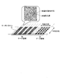
- FIG. 2 is a diagram for explaining a magnetic storage medium.
- FIG. 3 is a diagram for explaining a magnetic storage medium.
- FIG. 4 is a diagram for explaining a magnetic storage medium.
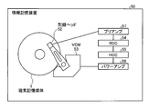
- FIG. 5 is a diagram showing the configuration of the information storage device.
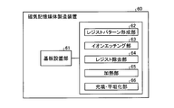
- FIG. 6 is a diagram showing the configuration of the magnetic storage medium manufacturing apparatus.
- FIG. 7 is a flowchart showing the flow of processing by the magnetic storage medium manufacturing apparatus.
- FIG. 8 is a diagram for explaining the method of manufacturing the magnetic storage medium according to the second embodiment.
- FIG. 1 is a diagram for explaining a method for manufacturing a magnetic storage medium.
- a recording film (magnetic film) 2 of a magnetic material for example, cobalt and platinum
- a nonmagnetic element for example, chromium, copper
- the magnetic film 2 may be an alloy containing cobalt or platinum as a main component.
- the nonmagnetic film 3 may be an alloy mainly composed of chromium, copper, gold, silver or the like.
- a resist pattern corresponding to the servo pattern 31 and the dot 21 is formed on the nonmagnetic film 3.
- the resist 4 is laminated so that the resist pattern of the servo pattern 31 is thicker than the resist pattern of the dots 21 to form a resist pattern.
- a film of a resist 4 is formed on the nonmagnetic film 3 with a uniform thickness, and a portion that becomes the nonmagnetic body 40 is irradiated with an electron beam or light having a higher dose than a portion that becomes the dot 21, The resist pattern is formed by irradiating the electron beam or light having a higher dose than the portion to be the servo pattern 31 to the portion to be the dot 21.
- Magnetic storage medium 2 to 4 are diagrams for explaining the magnetic storage medium.
- the magnetic storage medium 1 manufactured by the above manufacturing method has data areas 20 and servo areas 30 alternately as shown in FIG. 2 shows an example of the magnetic storage medium 1 having a phase servo pattern, it may be a magnetic storage medium having an area (or amplitude) servo pattern.
- the data area 20 is an area where data is read and written by the recording head, and has dots 21 of the magnetic film 2 isolated by the nonmagnetic material 40 as shown in FIG.
- the dot 21 is an aggregate of crystal grains of one magnetic material or crystal grains that are magnetically strongly coupled.
- the servo area 30 is an area in which servo information for head positioning is written. As shown in FIG. 4, the servo pattern 31 is wider in the circumferential direction than the dot 21 and extends in the radial direction. Have.
- the concentration of the nonmagnetic element in the crystal grain boundary of the magnetic film 2 is higher than the concentration of the nonmagnetic element in the crystal grain of the magnetic film 2.
- the servo pattern 31 nonmagnetic elements are segregated at the crystal grain boundaries of the magnetic film 2, and the crystal grains of the magnetic film 2 are magnetically isolated from each other.
- the magnetization in the servo pattern 31 is less likely to be directed in the circumferential direction and the radial direction, and the vertical magnetization in the servo pattern 31 is more stable than in the conventional magnetic storage medium. Can be kept in.
- FIG. 5 is a diagram showing the configuration of the information storage device.
- the information storage device 50 includes a magnetic storage medium 1, a recording head 52, a voice coil motor (VCM) 53, a read channel (RDC) 54, a hard disk controller (HDC) 55, a power amplifier 56, and a preamplifier 57.
- VCM voice coil motor
- RDC read channel
- HDC hard disk controller
- the recording head 52 reads and writes data stored in the magnetic storage medium 1, and the preamplifier 57 amplifies the reproduction signal read from the magnetic storage medium 1 by the recording head 52 and outputs the amplified signal to the RDC 54.
- the RDC 54 extracts servo information and data from the reproduction signal and outputs them to the HDC 55.
- HDC 55 is a controller that controls the operation of the entire information storage device 50, and outputs a signal for controlling the operation of the VCM 53 to the power amplifier 56 based on the servo information.
- the VCM 53 controls the position of the recording head 52 based on a signal received from the HDC 55 via the power amplifier 56.
- FIG. 6 is a diagram showing the configuration of the magnetic storage medium manufacturing apparatus.
- the magnetic storage medium manufacturing apparatus 60 includes a substrate placement portion 61 for placing a substrate having a laminated structure up to the backing layer, a resist pattern formation portion 62, an ion etching portion 63, a resist removal portion 64, a heating portion 65, A filling / flattening portion 66 is provided.
- the resist pattern forming unit 62 forms a magnetic film 2 of a magnetic material on a substrate, and forms a nonmagnetic film 3 of a nonmagnetic element on the magnetic film 2. Subsequently, the resist pattern forming unit 62 forms a resist pattern corresponding to the servo pattern 31 and the dots 21 on the nonmagnetic film 3. Specifically, the resist 4 is laminated so that the resist pattern of the servo pattern 31 is thicker than the resist pattern of the dots 21 to form a resist pattern.
- the ion etching unit 63 is a nonmagnetic film only on the magnetic film 2 forming the servo pattern 31 among the magnetic film 2 forming the servo pattern 31 in the servo area 30 and the magnetic film 2 forming the dot 21 in the data area 20. 3 is arranged. Specifically, ion etching is performed by irradiating the substrate with ions until the nonmagnetic film 3 remains only on the magnetic film 2 forming the servo pattern 31.
- the ion etching part 63 is also called a nonmagnetic film
- the resist removing unit 64 performs reactive ion etching to remove the resist 4 remaining on the magnetic film 2 forming the servo pattern 31.
- the heating unit 65 heats the substrate and segregates nonmagnetic elements at the crystal grain boundaries of the magnetic film 2 forming the servo pattern 31.
- the heating unit 65 is also referred to as a segregation unit.
- the filling / planarizing unit 66 fills the groove formed by the ion etching unit 63 with a nonmagnetic material and planarizes the surface. Then, the filling / planarizing unit 66 forms a protective film and a lubricant film on the substrate.
- FIG. 7 is a flowchart showing the flow of processing by the magnetic storage medium manufacturing apparatus.
- the resist pattern forming unit 62 detects the magnetic material on the substrate.
- a magnetic film 2 is formed, and a nonmagnetic film 3 of a nonmagnetic element is formed on the magnetic film 2 (step S102).
- the resist pattern forming unit 62 forms a resist pattern corresponding to the servo pattern 31 and the dots 21 on the nonmagnetic film 3 (step S103).
- the ion etching unit 63 performs ion etching until the nonmagnetic film 3 remains only on the magnetic film 2 forming the servo pattern 31 (see FIG. 4) (step S104). Subsequently, the resist removing unit 64 removes the remaining resist 4 (step S105), and the heating unit 65 heats the substrate (step S106).
- the filling / planarizing unit 66 fills the groove formed by the ion etching unit 63 with a nonmagnetic material. Then, the surface is flattened (step S107). Then, the filling / planarizing unit 66 forms a protective film and a lubricant film on the substrate (step S108), and ends the process.
- the magnetic storage medium according to the first embodiment can stably maintain the magnetization in the vertical direction in the servo pattern.
- the magnetic storage medium according to the first embodiment since the crystal grains in the servo pattern are magnetically isolated from each other, even if there are crystal grains whose magnetization is reversed in the servo pattern, the starting point is It is possible to prevent the reverse magnetic domain from expanding. Also in this respect, the magnetic storage medium according to the first embodiment can keep the magnetization of the servo pattern stable in the vertical direction.
- the magnetic storage medium manufacturing method and the magnetic storage medium manufacturing apparatus according to the first embodiment, it is possible to provide a magnetic storage medium capable of stably maintaining the perpendicular magnetization in the servo pattern.
- a medium in which dots and servo patterns are formed based on the same magnetic material can be manufactured.
- a magnetic storage medium that can keep the magnetization in the vertical direction stable can be manufactured.
- FIG. 8 is a diagram for explaining the method of manufacturing the magnetic storage medium according to the second embodiment.
- a film is formed (coated) in the order of the magnetic film 2, the nonmagnetic film 3, the resist 4-1 having low exposure sensitivity, and the resist 4-2 having high exposure sensitivity.
- the portion that becomes the nonmagnetic material 40 is irradiated with an electron beam or light having a higher dose than the portion that becomes the dot 21, and the servo pattern 31 is applied to the portion that becomes the dot 21.
- a resist pattern is drawn by irradiating an electron beam or light having a dose higher than that of the portion to be. In this way, the thickness of the resist 4 remaining on the substrate can be controlled with high accuracy.
- a resist pattern may be formed using a nanoimprint lithography method. That is, a master disk (imprint mold) in which a groove deeper than the portion corresponding to the dot 21 is formed at a position corresponding to the servo pattern 31 is formed, and the magnetic film 2, the nonmagnetic film 3, and the resist 4 are formed.
- the resist pattern is transferred by pressing the master against the filmed substrate. In this way, it is possible to easily form the resist 4 in which the resist pattern of the servo pattern 31 is thicker than the resist pattern of the dots 21.
Landscapes
- Engineering & Computer Science (AREA)
- Chemical & Material Sciences (AREA)
- Nanotechnology (AREA)
- Physics & Mathematics (AREA)
- Mathematical Physics (AREA)
- Theoretical Computer Science (AREA)
- Crystallography & Structural Chemistry (AREA)
- Manufacturing Of Magnetic Record Carriers (AREA)
- Magnetic Record Carriers (AREA)
Abstract
サーボ領域におけるサーボパターンの媒体面内方向の幅が、データ領域におけるドットの媒体面内方向の幅よりも広く形成された磁気記憶媒体において、サーボパターンにおける垂直方向の磁化を安定に保つことを課題とする。この課題を解決するため、サーボパターンを形成する磁性膜の結晶粒界における非磁性元素の濃度が、該磁性膜の結晶粒内における非磁性元素の濃度よりも高くなるようにする。このような磁気記憶媒体は、サーボパターンを形成する磁性膜およびドットを形成する磁性膜のうち、サーボパターンを形成する磁性膜上にのみ非磁性膜を配置させる非磁性膜配置ステップと、非磁性膜配置ステップによって配置された非磁性膜を加熱することで、サーボパターンを形成する磁性膜の結晶粒界に非磁性元素を偏析させる偏析ステップとを含む磁気記憶媒体の製造方法によって提供することができる。
Description
この発明は、垂直磁気記録方式によりデータを記録する磁気記憶媒体、その磁気記憶媒体の製造方法、その磁気記憶媒体を有する情報記憶装置、および、その磁気記憶媒体を製造する磁気記憶媒体製造装置に関する。
近年の磁気記憶媒体の高記録密度化に伴い、磁性膜を媒体の垂直方向に磁化することでデータを記録する垂直磁気記録方式が主流技術となってきている。そして、さらなる高記録密度化を実現するためのビットパターンドメディアが注目されている(特許文献1参照)。
このビットパターンドメディアは、データ領域と、サーボ領域とを交互に有し、データ領域に、非磁性材料で隔離された磁性膜のドットを高密度で有することで高記録密度化を実現している。また、ビットパターンドメディアは、サーボ領域に、データ領域のドットに比べてディスク面内方向の幅が広い磁性膜パターンを有することが一般的であり、特に半径方向に伸びた磁性膜パターンを有することが多い。
上記の通り、ビットパターンドメディアのサーボパターンは、データ領域のドットに比べて媒体面内方向の幅が広い磁性膜パターンを有するため、垂直方向よりも媒体面内方向に磁化が向きやすい形状磁気異方性を生じる。そのため、従来のビットパターンドメディアには、サーボパターンにおける磁化を垂直方向に安定に保つための保磁力が弱いという課題があった。
そこで、開示の技術は、上述した従来技術の課題を解決するためになされたものであり、サーボパターンにおける磁化を垂直方向に安定に保つことが可能な磁気記憶媒体、その磁気記憶媒体の製造方法、その磁気記憶媒体を有する情報記憶装置、および、その磁気記憶媒体を製造する磁気記憶媒体製造装置を提供することを目的とする。
上述した課題を解決し、目的を達成するため、開示の磁気記憶媒体は、サーボ領域におけるサーボパターンの媒体面内方向の幅が、データ領域におけるドットの媒体面内方向の幅よりも広く形成され、かつ、当該サーボパターンを形成する磁性膜の結晶粒界における非磁性元素の濃度が、当該磁性膜の結晶粒内における非磁性元素の濃度よりも高いことを要件とする。
開示の磁気記憶媒体は、サーボパターンにおける垂直方向の磁化を安定に保つことが可能である。
1 磁気記憶媒体
2 磁性膜
3 非磁性膜
4 レジスト
20 データ領域
21 ドット
30 サーボ領域
31 サーボパターン
40 非磁性体
50 情報記憶装置
52 記録ヘッド
53 ボイスコイルモータ(VCM)
54 リードチャネル(RDC)
55 ハードディスクコントローラ(HDC)
56 パワーアンプ
57 プリアンプ
60 磁気記憶媒体製造装置
61 基板設置部
62 レジストパターン形成部
63 イオンエッチング部
64 レジスト除去部
65 加熱部
66 充填・平坦化部
2 磁性膜
3 非磁性膜
4 レジスト
20 データ領域
21 ドット
30 サーボ領域
31 サーボパターン
40 非磁性体
50 情報記憶装置
52 記録ヘッド
53 ボイスコイルモータ(VCM)
54 リードチャネル(RDC)
55 ハードディスクコントローラ(HDC)
56 パワーアンプ
57 プリアンプ
60 磁気記憶媒体製造装置
61 基板設置部
62 レジストパターン形成部
63 イオンエッチング部
64 レジスト除去部
65 加熱部
66 充填・平坦化部
以下に添付図面を参照して、磁気記憶媒体、磁気記憶媒体の製造方法、情報記憶装置および磁気記憶媒体製造装置の一実施の形態を詳細に説明する。
[磁気記憶媒体の製造方法]
(a)レジストパターン形成工程
図1は、磁気記憶媒体の製造方法を説明するための図である。図1の(a)に示すように、基板上に磁性材料(例えば、コバルトおよび白金)の記録膜(磁性膜)2を成膜し、磁性膜2上に非磁性元素(例えば、クロム、銅、金、銀など)の非磁性膜3を成膜する。なお、磁性膜2は、コバルトや白金を主成分とする合金であってもよい。また、非磁性膜3は、クロム、銅、金、銀などを主成分とする合金であってもよい。
(a)レジストパターン形成工程
図1は、磁気記憶媒体の製造方法を説明するための図である。図1の(a)に示すように、基板上に磁性材料(例えば、コバルトおよび白金)の記録膜(磁性膜)2を成膜し、磁性膜2上に非磁性元素(例えば、クロム、銅、金、銀など)の非磁性膜3を成膜する。なお、磁性膜2は、コバルトや白金を主成分とする合金であってもよい。また、非磁性膜3は、クロム、銅、金、銀などを主成分とする合金であってもよい。
続いて、非磁性膜3の上に、サーボパターン31およびドット21に対応したレジストパターンを形成する。具体的には、ドット21のレジストパターンよりもサーボパターン31のレジストパターンの方が厚くなるようにレジスト4を積層して、レジストパターンを形成する。例えば、非磁性膜3上に一様の厚さでレジスト4の膜を成膜し、非磁性体40となる箇所にドット21となる箇所よりも高いドーズ量の電子線もしくは光を照射し、ドット21となる箇所にサーボパターン31となる箇所よりも高いドーズ量の電子線もしくは光を照射することで、レジストパターンを形成する。
(b)イオンエッチング工程
次に、図1の(b)に示すように、サーボ領域30におけるサーボパターン31を形成する磁性膜2およびデータ領域20におけるドット21を形成する磁性膜2のうち、サーボパターン31を形成する磁性膜2上にのみ非磁性膜3を配置する。例えば、サーボパターン31を形成する磁性膜2上のみに非磁性膜3が残るまでイオンエッチングを行なう。このとき、ドット21および非磁性体40となる箇所の非磁性膜3は基板上から除去される。
次に、図1の(b)に示すように、サーボ領域30におけるサーボパターン31を形成する磁性膜2およびデータ領域20におけるドット21を形成する磁性膜2のうち、サーボパターン31を形成する磁性膜2上にのみ非磁性膜3を配置する。例えば、サーボパターン31を形成する磁性膜2上のみに非磁性膜3が残るまでイオンエッチングを行なう。このとき、ドット21および非磁性体40となる箇所の非磁性膜3は基板上から除去される。
(c)レジスト除去・加熱工程
続いて、有機溶剤による洗浄や酸素等のガスを用いた反応性イオンエッチング(アッシング)を行ない、図1の(c)に示すように、サーボパターン31を形成する磁性膜2上に残存したレジスト4を除去する。そして、媒体を加熱して、サーボパターン31を形成する磁性膜2の結晶粒界に非磁性元素を偏析させる。このとき、磁性膜2を構成する磁性材料の結晶粒同士は、非磁性元素によって隔離されるため、磁気的に孤立する。
続いて、有機溶剤による洗浄や酸素等のガスを用いた反応性イオンエッチング(アッシング)を行ない、図1の(c)に示すように、サーボパターン31を形成する磁性膜2上に残存したレジスト4を除去する。そして、媒体を加熱して、サーボパターン31を形成する磁性膜2の結晶粒界に非磁性元素を偏析させる。このとき、磁性膜2を構成する磁性材料の結晶粒同士は、非磁性元素によって隔離されるため、磁気的に孤立する。
(d)充填・平坦化工程
次に、図1の(d)に示すように、イオンエッチング工程により形成された溝に非磁性材料を充填し、科学・機械研磨法(Chemical Mechanical Polishing :CMP)などを用いて、表面を平坦化する。最後に、基板上に保護膜および潤滑剤の膜を形成する。これにより、サーボパターン31を形成する磁性膜の結晶粒界における非磁性元素の濃度が、磁性膜の結晶粒内における非磁性元素の濃度よりも高い磁気記憶媒体1を製造することができる。
次に、図1の(d)に示すように、イオンエッチング工程により形成された溝に非磁性材料を充填し、科学・機械研磨法(Chemical Mechanical Polishing :CMP)などを用いて、表面を平坦化する。最後に、基板上に保護膜および潤滑剤の膜を形成する。これにより、サーボパターン31を形成する磁性膜の結晶粒界における非磁性元素の濃度が、磁性膜の結晶粒内における非磁性元素の濃度よりも高い磁気記憶媒体1を製造することができる。
[磁気記憶媒体]
図2~図4は、磁気記憶媒体を説明するための図である。上記の製造方法により製造された磁気記憶媒体1は、図2に示すように、データ領域20と、サーボ領域30とを交互に有する。なお、図2では、位相サーボパターンを有する磁気記憶媒体1の一例を示しているが、面積(または振幅)サーボパターンを有する磁気記憶媒体であってもよい。
図2~図4は、磁気記憶媒体を説明するための図である。上記の製造方法により製造された磁気記憶媒体1は、図2に示すように、データ領域20と、サーボ領域30とを交互に有する。なお、図2では、位相サーボパターンを有する磁気記憶媒体1の一例を示しているが、面積(または振幅)サーボパターンを有する磁気記憶媒体であってもよい。
データ領域20は、記録ヘッドによりデータの読み書きが行なわれる領域であり、図3に示すように、非磁性体40によって隔離された磁性膜2のドット21を有する。ドット21は、一つの磁性材料の結晶粒または磁気的に強く結合した結晶粒の集合体である。サーボ領域30は、ヘッドの位置決め用のサーボ情報が書き込まれた領域であり、図4に示すように、ドット21に比べて円周方向の幅が広く、かつ半径方向に伸びたサーボパターン31を有する。
このサーボパターン31内では、磁性膜2の結晶粒界における非磁性元素の濃度が、磁性膜2の結晶粒内における非磁性元素の濃度よりも高い。言い換えると、図4に示すように、サーボパターン31内では、磁性膜2の結晶粒界に非磁性元素が偏析し、磁性膜2の結晶粒同士が磁気的に孤立している。これにより、実施例1に係る磁気記憶媒体1では、サーボパターン31における磁化が円周方向や半径方向に向きにくくなっており、従来の磁気記憶媒体よりもサーボパターン31における垂直方向の磁化を安定に保つことができる。
[情報記憶装置]
図5は、情報記憶装置の構成を示した図である。情報記憶装置50は、図5に示すように、磁気記憶媒体1、記録ヘッド52、ボイスコイルモータ(VCM)53、リードチャネル(RDC)54、ハードディスクコントローラ(HDC)55、パワーアンプ56、プリアンプ57を有する。
図5は、情報記憶装置の構成を示した図である。情報記憶装置50は、図5に示すように、磁気記憶媒体1、記録ヘッド52、ボイスコイルモータ(VCM)53、リードチャネル(RDC)54、ハードディスクコントローラ(HDC)55、パワーアンプ56、プリアンプ57を有する。
記録ヘッド52は、磁気記憶媒体1に記憶されるデータの読み書きを行い、プリアンプ57は、記録ヘッド52が磁気記憶媒体1から読み出した再生信号を増幅してRDC54に出力する。RDC54は、再生信号からサーボ情報やデータを取り出してHDC55に出力する。
HDC55は、情報記憶装置50全体の動作を制御するコントローラであり、サーボ情報に基づいてVCM53の動作を制御するための信号をパワーアンプ56に出力する。VCM53は、パワーアンプ56を介してHDC55から受け付けた信号に基づいて記録ヘッド52の位置を制御する。
[磁気記憶媒体製造装置]
図6は、磁気記憶媒体製造装置の構成を示した図である。図6に示すように。磁気記憶媒体製造装置60は、裏打層までの積層構造が形成された基板を設置するための基板設置部61と、レジストパターン形成部62、イオンエッチング部63、レジスト除去部64、加熱部65および充填・平坦化部66を有する。
図6は、磁気記憶媒体製造装置の構成を示した図である。図6に示すように。磁気記憶媒体製造装置60は、裏打層までの積層構造が形成された基板を設置するための基板設置部61と、レジストパターン形成部62、イオンエッチング部63、レジスト除去部64、加熱部65および充填・平坦化部66を有する。
レジストパターン形成部62は、基板上に磁性材料の磁性膜2を成膜し、磁性膜2上に非磁性元素の非磁性膜3を成膜する。続いて、レジストパターン形成部62は、非磁性膜3の上に、サーボパターン31およびドット21に対応したレジストパターンを形成する。具体的には、ドット21のレジストパターンよりもサーボパターン31のレジストパターンの方が厚くなるようにレジスト4を積層して、レジストパターンを形成する。
イオンエッチング部63は、サーボ領域30におけるサーボパターン31を形成する磁性膜2およびデータ領域20におけるドット21を形成する磁性膜2のうち、サーボパターン31を形成する磁性膜2上にのみ非磁性膜3を配置する。具体的には、サーボパターン31を形成する磁性膜2上のみに非磁性膜3が残るまで基板に対してイオンを照射してイオンエッチングを行なう。なお、イオンエッチング部63は、非磁性膜配置部ともいう。
レジスト除去部64は、反応性イオンエッチングを行ない、サーボパターン31を形成する磁性膜2上に残存したレジスト4を除去する。加熱部65は、基板を加熱して、サーボパターン31を形成する磁性膜2の結晶粒界に非磁性元素を偏析させる。なお、加熱部65は、偏析部ともいう。
充填・平坦化部66は、イオンエッチング部63により形成された溝に非磁性材料を充填し、表面を平坦化する。そして、充填・平坦化部66は、基板上に保護膜および潤滑剤の膜を形成する。
[磁気記憶媒体製造装置による処理]
図7は、磁気記憶媒体製造装置による処理の流れを示すフローチャート図である。図7に示すように、裏打層までの積層構造が形成された基板が基板設置部61に設置されたことを検知すると(ステップS101肯定)、レジストパターン形成部62は、基板上に磁性材料の磁性膜2を成膜し、磁性膜2上に非磁性元素の非磁性膜3を成膜する(ステップS102)。続いて、レジストパターン形成部62は、非磁性膜3の上に、サーボパターン31およびドット21に対応したレジストパターンを形成する(ステップS103)。
図7は、磁気記憶媒体製造装置による処理の流れを示すフローチャート図である。図7に示すように、裏打層までの積層構造が形成された基板が基板設置部61に設置されたことを検知すると(ステップS101肯定)、レジストパターン形成部62は、基板上に磁性材料の磁性膜2を成膜し、磁性膜2上に非磁性元素の非磁性膜3を成膜する(ステップS102)。続いて、レジストパターン形成部62は、非磁性膜3の上に、サーボパターン31およびドット21に対応したレジストパターンを形成する(ステップS103)。
レジストパターンが形成されると、イオンエッチング部63は、サーボパターン31(図4参照)を形成する磁性膜2上のみに非磁性膜3が残るまでイオンエッチングを行なう(ステップS104)。続いて、レジスト除去部64は、は、残存したレジスト4を除去し(ステップS105)、加熱部65は、基板を加熱する(ステップS106)。
サーボパターン31(図4参照)を形成する磁性膜2の結晶粒界に非磁性元素が偏析すると、充填・平坦化部66は、イオンエッチング部63により形成された溝に非磁性材料を充填し、表面を平坦化する(ステップS107)。そして、充填・平坦化部66は、基板上に保護膜および潤滑剤の膜を形成し(ステップS108)、処理を終了する。
[実施例1による効果]
上述したように、実施例1に係る磁気記憶媒体は、サーボパターンにおける垂直方向の磁化を安定に保つことが可能である。また、実施例1に係る磁気記憶媒体では、サーボパターンにおける結晶粒同士が磁気的に孤立しているため、仮に、サーボパターン内に磁化反転した結晶粒がある場合であっても、それを起点に逆向き磁区が拡大するのを阻止することができる。この点においても、実施例1に係る磁気記憶媒体は、サーボパターンの磁化を垂直方向に安定に保つことが可能である。
上述したように、実施例1に係る磁気記憶媒体は、サーボパターンにおける垂直方向の磁化を安定に保つことが可能である。また、実施例1に係る磁気記憶媒体では、サーボパターンにおける結晶粒同士が磁気的に孤立しているため、仮に、サーボパターン内に磁化反転した結晶粒がある場合であっても、それを起点に逆向き磁区が拡大するのを阻止することができる。この点においても、実施例1に係る磁気記憶媒体は、サーボパターンの磁化を垂直方向に安定に保つことが可能である。
また、実施例1に係る磁気記憶媒体の製造方法および磁気記憶媒体製造装置を用いれば、サーボパターンにおける垂直方向の磁化を安定に保つことが可能な磁気記憶媒体を提供することができる。また、実施例1に係る磁気記憶媒体の製造方法によれば、ドットおよびサーボパターンが同一の磁性材料をもとに形成される媒体を製造することができるので、簡易な製造工程によりサーボパターンにおける垂直方向の磁化を安定に保つことが可能な磁気記憶媒体を製造することができる。
また、実施例1に係る磁気記憶媒体の製造方法を用いれば、サーボパターンの形状を変える必要がないため、従来のサーボ方式をそのまま流用することができる。
以下では、実施例2として、他の実施形態を説明する。
図8は、実施例2に係る磁気記憶媒体の製造方法を説明するための図である。図8の(a)に示すように、磁性膜2、非磁性膜3、露光感度が低いレジスト4-1、および、露光感度が高いレジスト4-2の順番に基板上に膜を形成(塗布)する。そして、図8の(b)に示すように、非磁性体40となる箇所に、ドット21となる箇所よりも高いドーズ量の電子線もしくは光を照射し、ドット21となる箇所にサーボパターン31となる箇所よりも高いドーズ量の電子線もしくは光を照射して、レジストパターンを描画する。このようにすることで、基板上に残るレジスト4の厚さを高精度に制御することが可能である。
また、ナノインプリントリソグラフィ法を用いて、レジストパターンを形成するようにしてもよい。すなわち、サーボパターン31に対応する箇所に、ドット21に対応する箇所よりも深い溝が掘られた原盤(インプリントモールド)を作成し、磁性膜2、非磁性膜3、および、レジスト4が成膜された基板に対して、その原盤を押し付けてレジストパターンを転写する。このようにすることで、ドット21のレジストパターンよりもサーボパターン31のレジストパターンの方が厚くなるようなレジスト4を容易に形成することができる。
Claims (14)
- サーボ領域におけるサーボパターンの円周方向の幅が、データ領域におけるドットの円周方向の幅よりも広く形成され、かつ、当該サーボパターンを形成する磁性膜の結晶粒界における非磁性元素の濃度が、当該磁性膜の結晶粒内における非磁性元素の濃度よりも高いことを特徴とする磁気記憶媒体。
- サーボ領域におけるサーボパターンを形成する磁性膜およびデータ領域におけるドットを形成する磁性膜のうち、前記サーボパターンを形成する磁性膜上にのみ非磁性膜を配置させる非磁性膜配置ステップと、
前記非磁性膜配置ステップによって配置された非磁性膜を加熱することで、前記サーボパターンを形成する磁性膜の結晶粒界に非磁性元素を偏析させる偏析ステップと、
を含むことを特徴とする磁気記憶媒体の製造方法。 - 磁性膜の上に非磁性膜が積層された基板の前記非磁性膜の上に、前記サーボパターンおよびドットに対応したレジストパターンを形成する場合に、前記ドットのレジストパターンよりも前記サーボパターンのレジストパターンを厚く形成するレジストパターン形成ステップをさらに含み、
前記非磁性膜形成ステップは、前記ドットを形成する磁性膜上の非磁性膜は除去され、かつ、前記サーボパターンを形成する磁性膜上のみに非磁性膜が配置されるように、前記基板上の前記レジストパターン、非磁性膜および磁性膜をエッチングすることを特徴とする請求項2に記載の磁気記憶媒体の製造方法。 - 前記レジストパターン形成ステップは、磁性膜の上に非磁性膜、第一のレジスト、および、当該第一のレジストよりも露光感度が高い第二のレジストが積層された基板に対して、前記サーボ領域と、前記データ領域とで異なるドーズ量の露光を行なうことで、前記ドットのレジストパターンよりも前記サーボパターンのレジストパターンを厚く形成することを特徴とする請求項3に記載の磁気記憶媒体の製造方法。
- 前記レジストパターン形成ステップは、磁性膜の上に非磁性膜およびレジストが積層された基板に対して、前記サーボパターンに対応する箇所に、前記ドットに対応する箇所よりも深い溝が掘られた原盤を押し付けることで、前記ドットのレジストパターンよりも前記サーボパターンのレジストパターンを厚く形成することを特徴とする請求項3に記載の磁気記憶媒体の製造方法。
- 前記非磁性膜が、クロム、銅、金、銀のいずれかの金属、またはその合金を主成分とする材料からなることを特徴とする請求項2に記載の磁気記憶媒体の製造方法。
- 前記磁性膜が、コバルト、白金のいずれかの金属、またはその合金を主成分とする材料からなることを特徴とする請求項2に記載の磁気記憶媒体の製造方法。
- サーボ領域におけるサーボパターンを形成する磁性膜およびデータ領域におけるドットを形成する磁性膜のうち、前記サーボパターンを形成する磁性膜上にのみ非磁性膜を配置させる非磁性膜配置部と、
前記非磁性膜配置部によって配置された非磁性膜を加熱することで、前記サーボパターンを形成する磁性膜の結晶粒界に非磁性元素を偏析させる偏析部と、
を有することを特徴とする磁気記憶媒体製造装置。 - 磁性膜の上に非磁性膜が積層された基板の前記非磁性膜の上に、前記サーボパターンおよびドットに対応したレジストパターンを形成する場合に、前記ドットのレジストパターンよりも前記サーボパターンのレジストパターンを厚く形成するレジストパターン形成部をさらに有し、
前記非磁性膜形成部は、前記ドットを形成する磁性膜上の非磁性膜は除去され、かつ、前記サーボパターンを形成する磁性膜上のみに非磁性膜が配置されるように、前記基板上の前記レジストパターン、非磁性膜および磁性膜をエッチングすることを特徴とする請求項8に記載の磁気記憶媒体製造装置。 - 前記レジストパターン形成部は、磁性膜の上に非磁性膜、第一のレジスト、および、当該第一のレジストよりも露光感度が高い第二のレジストが積層された基板に対して、前記サーボ領域と、前記データ領域とで異なるドーズ量の露光を行なうことで、前記ドットのレジストパターンよりも前記サーボパターンのレジストパターンを厚く形成することを特徴とする請求項9に記載の磁気記憶媒体製造装置。
- 前記レジストパターン形成部は、磁性膜の上に非磁性膜およびレジストが積層された基板に対して、前記サーボパターンに対応する箇所に、前記ドットに対応する箇所よりも深い溝が掘られた原盤を押し付けることで、前記ドットのレジストパターンよりも前記サーボパターンのレジストパターンを厚く形成することを特徴とする請求項9に記載の磁気記憶媒体製造装置。
- 前記非磁性膜が、クロム、銅、金、銀のいずれかの金属、またはその合金を主成分とする材料からなることを特徴とする請求項8に記載の磁気記憶媒体製造装置。
- 前記磁性膜が、コバルト、白金のいずれかの金属、またはその合金を主成分とする材料からなることを特徴とする請求項8に記載の磁気記憶媒体製造装置。
- サーボ領域におけるサーボパターンの媒体面内方向の幅が、データ領域におけるドットの媒体面内方向の幅よりも広く形成され、かつ、当該サーボパターンを形成する磁性膜の結晶粒界における非磁性元素の濃度が、当該磁性膜の結晶粒内における非磁性元素の濃度よりも高い磁気記憶媒体を有することを特徴とする情報記憶装置。
Priority Applications (1)
| Application Number | Priority Date | Filing Date | Title |
|---|---|---|---|
| PCT/JP2009/051806 WO2010089850A1 (ja) | 2009-02-03 | 2009-02-03 | 磁気記憶媒体、磁気記憶媒体の製造方法、情報記憶装置、および、磁気記憶媒体製造装置 |
Applications Claiming Priority (1)
| Application Number | Priority Date | Filing Date | Title |
|---|---|---|---|
| PCT/JP2009/051806 WO2010089850A1 (ja) | 2009-02-03 | 2009-02-03 | 磁気記憶媒体、磁気記憶媒体の製造方法、情報記憶装置、および、磁気記憶媒体製造装置 |
Publications (1)
| Publication Number | Publication Date |
|---|---|
| WO2010089850A1 true WO2010089850A1 (ja) | 2010-08-12 |
Family
ID=42541774
Family Applications (1)
| Application Number | Title | Priority Date | Filing Date |
|---|---|---|---|
| PCT/JP2009/051806 Ceased WO2010089850A1 (ja) | 2009-02-03 | 2009-02-03 | 磁気記憶媒体、磁気記憶媒体の製造方法、情報記憶装置、および、磁気記憶媒体製造装置 |
Country Status (1)
| Country | Link |
|---|---|
| WO (1) | WO2010089850A1 (ja) |
Citations (3)
| Publication number | Priority date | Publication date | Assignee | Title |
|---|---|---|---|---|
| JP2000268340A (ja) * | 1999-03-12 | 2000-09-29 | Fujitsu Ltd | 磁気記録媒体及びその製造方法 |
| JP2006172686A (ja) * | 2004-11-22 | 2006-06-29 | Fujitsu Ltd | 磁気記録媒体およびその製造方法、磁気記憶装置、基板、テクスチャ形成装置 |
| JP2007242182A (ja) * | 2006-03-10 | 2007-09-20 | Fujitsu Ltd | 磁気記録媒体製造方法および磁気記録媒体 |
-
2009
- 2009-02-03 WO PCT/JP2009/051806 patent/WO2010089850A1/ja not_active Ceased
Patent Citations (3)
| Publication number | Priority date | Publication date | Assignee | Title |
|---|---|---|---|---|
| JP2000268340A (ja) * | 1999-03-12 | 2000-09-29 | Fujitsu Ltd | 磁気記録媒体及びその製造方法 |
| JP2006172686A (ja) * | 2004-11-22 | 2006-06-29 | Fujitsu Ltd | 磁気記録媒体およびその製造方法、磁気記憶装置、基板、テクスチャ形成装置 |
| JP2007242182A (ja) * | 2006-03-10 | 2007-09-20 | Fujitsu Ltd | 磁気記録媒体製造方法および磁気記録媒体 |
Similar Documents
| Publication | Publication Date | Title |
|---|---|---|
| US7986493B2 (en) | Discrete track magnetic media with domain wall pinning sites | |
| JP2006127681A (ja) | 磁気記録媒体及びその製造方法、磁気記録再生装置 | |
| JP2012033249A (ja) | 磁気転写用マスター基板、それを用いた磁気転写方法および磁気転写媒体 | |
| CN100354935C (zh) | 用于垂直磁记录的图形化盘介质和具有其的磁盘驱动器 | |
| US9269387B2 (en) | Magnetic recording medium and method of fabricating the same | |
| JP2009129501A (ja) | 磁気記録媒体、磁気記録媒体の製造方法および製造装置、ならびに磁気記録装置 | |
| US20050185332A1 (en) | Perpendicular pole structure and method of fabricating the same | |
| CN102016987A (zh) | 磁记录介质及磁记录再生装置、磁记录介质的制造方法 | |
| JP2009157983A (ja) | 磁気記録媒体の製造方法及び磁気記録再生装置 | |
| JP5140527B2 (ja) | 磁気記録媒体、磁気記録媒体の製造方法および磁気記録再生装置 | |
| JP5394729B2 (ja) | 磁気記憶媒体製造方法、磁気記憶媒体、および情報記憶装置 | |
| WO2010089850A1 (ja) | 磁気記憶媒体、磁気記憶媒体の製造方法、情報記憶装置、および、磁気記憶媒体製造装置 | |
| US8839504B2 (en) | Method of fabricating a device having a sidegap | |
| JP4557994B2 (ja) | 磁気記録媒体の製造方法 | |
| JP2007012116A (ja) | 磁気記録装置 | |
| JP5114285B2 (ja) | 磁気記録媒体、磁気記録媒体の製造方法および磁気記録再生装置 | |
| JP2004288250A (ja) | 磁気転写用マスタディスク及びその製造方法 | |
| JP2006286085A (ja) | 磁性パターン形成方法、磁気記録媒体、磁気記録再生装置 | |
| US8274865B2 (en) | Master disk for magnetic recording medium | |
| CN102473422A (zh) | 磁记录介质的制造方法及磁记录再生装置 | |
| JP2005158095A (ja) | マスター情報担体の製造方法 | |
| JP5381081B2 (ja) | 磁気記録媒体、磁気記憶装置および磁気記録媒体の製造方法 | |
| US20090305082A1 (en) | Magnetic recording medium, magnetic recording and reproducing device with magnetic recording medium, and magnetic-recording-medium manufacturing method | |
| US20050184840A1 (en) | Perpendicular pole structure and method of fabricating the same | |
| JP2010123158A (ja) | 磁気記録媒体および磁気記録媒体の製造方法、磁気記録再生装置 |
Legal Events
| Date | Code | Title | Description |
|---|---|---|---|
| 121 | Ep: the epo has been informed by wipo that ep was designated in this application |
Ref document number: 09839628 Country of ref document: EP Kind code of ref document: A1 |
|
| NENP | Non-entry into the national phase |
Ref country code: DE |
|
| 122 | Ep: pct application non-entry in european phase |
Ref document number: 09839628 Country of ref document: EP Kind code of ref document: A1 |
|
| NENP | Non-entry into the national phase |
Ref country code: JP |