WO2010082629A1 - Naf変換装置 - Google Patents
Naf変換装置 Download PDFInfo
- Publication number
- WO2010082629A1 WO2010082629A1 PCT/JP2010/050420 JP2010050420W WO2010082629A1 WO 2010082629 A1 WO2010082629 A1 WO 2010082629A1 JP 2010050420 W JP2010050420 W JP 2010050420W WO 2010082629 A1 WO2010082629 A1 WO 2010082629A1
- Authority
- WO
- WIPO (PCT)
- Prior art keywords
- state
- bit
- input
- output
- naf
- Prior art date
- Legal status (The legal status is an assumption and is not a legal conclusion. Google has not performed a legal analysis and makes no representation as to the accuracy of the status listed.)
- Ceased
Links
Images






Classifications
-
- H—ELECTRICITY
- H03—ELECTRONIC CIRCUITRY
- H03M—CODING; DECODING; CODE CONVERSION IN GENERAL
- H03M7/00—Conversion of a code where information is represented by a given sequence or number of digits to a code where the same, similar or subset of information is represented by a different sequence or number of digits
- H03M7/02—Conversion to or from weighted codes, i.e. the weight given to a digit depending on the position of the digit within the block or code word
- H03M7/04—Conversion to or from weighted codes, i.e. the weight given to a digit depending on the position of the digit within the block or code word the radix thereof being two
-
- G—PHYSICS
- G06—COMPUTING OR CALCULATING; COUNTING
- G06F—ELECTRIC DIGITAL DATA PROCESSING
- G06F7/00—Methods or arrangements for processing data by operating upon the order or content of the data handled
- G06F7/38—Methods or arrangements for performing computations using exclusively denominational number representation, e.g. using binary, ternary, decimal representation
- G06F7/48—Methods or arrangements for performing computations using exclusively denominational number representation, e.g. using binary, ternary, decimal representation using non-contact-making devices, e.g. tube, solid state device; using unspecified devices
- G06F7/52—Multiplying; Dividing
- G06F7/523—Multiplying only
- G06F7/533—Reduction of the number of iteration steps or stages, e.g. using the Booth algorithm, log-sum, odd-even
- G06F7/5332—Reduction of the number of iteration steps or stages, e.g. using the Booth algorithm, log-sum, odd-even by skipping over strings of zeroes or ones, e.g. using the Booth Algorithm
Definitions
- the present invention relates to a NAF converter that converts an integer binary representation into a redundant binary representation.
- NAF which is a kind of redundant binary representation, is often used in the context of speeding up cryptographic processing (see, for example, Non-Patent Document 3 and Non-Patent Document 2).
- NAF is described on page 98 of Non-Patent Document 2, for example.
- NAF is a kind of redundant binary representation, and the integer k has only one corresponding NAF representation NAF (k).
- the number of non-zero digits in NAF (k) has proven to be the smallest among any redundant binary representations.
- the average number of non-zero digits is 1/3.
- the NAF expression has a feature that at least one of the subsequent two digits is 0, which is also a reason for the low density. It is also the origin of the name Non-adjacent form.
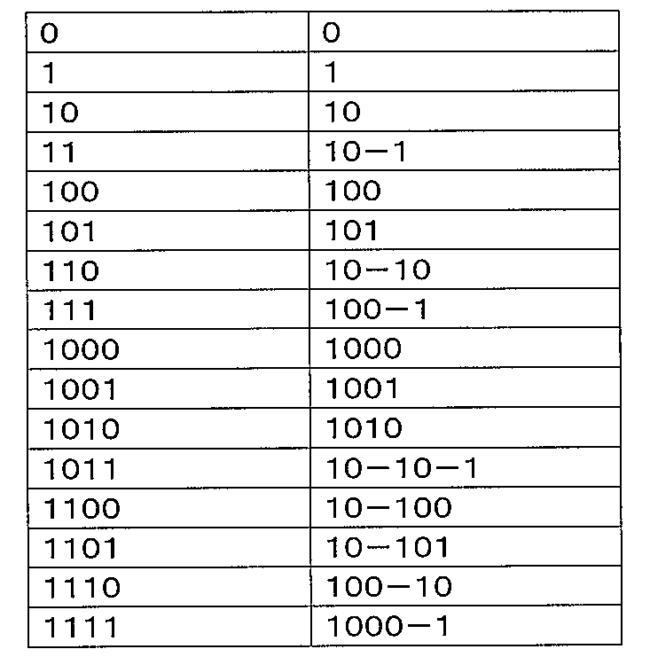
- Table 1 shows an example in which a binary number of 4 bits or less is converted to NAF.
- w-NAF has more numbers available for each digit.
- 3-NAF five types of -3, -1, 0, 1, 3 can be used.
- the above NAF can be considered a 2-NAF.
- Table 2 and Table 3 show the characteristics of w-NAF.
- Table 2 lists the numbers used in each NAF.
- ⁇ is power ( ⁇ ), for example 2 ⁇ w means 2 to the power of w.
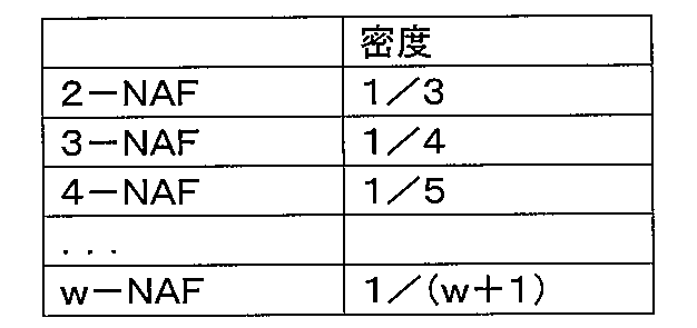
- Table 3 lists the non-zero digit density of each NAF.
- W-NAF is characterized in that at least one non-zero digit among the following w digits is at most.
- the w-NAF conversion algorithm includes page 100 (Algorithm 3.35) of Non-Patent Document 3 and page 153 (Algorithm 9.20) of Non-Patent Document 2.
- Non-Patent Document 3 and the algorithm 9.20 of Non-Patent Document 2 are characterized by high scalability that can be applied to any w, but on the other hand, there are the following problems: is there.
- ⁇ K cannot be input sequentially. In other words, k must be read first. This is because k itself is changed.
- Non-Patent Document 4 In Table 3.2 of Non-Patent Document 4, there is no description that NAF conversion is in Non-Patent Document 4, but what is output as a result is NAF conversion.
- the algorithm 9.14 of Non-Patent Document 2 has the same features and disadvantages.
- the known NAF conversion algorithm has a problem that scalability and circuit scale are not compatible.
- the present invention has been made in view of such circumstances, and an object thereof is to provide a scalable w-NAF conversion device with a small circuit scale.
- a NAF conversion device is a NAF conversion device that converts a binary representation of an integer into a redundant binary representation expressed in w-NAF, and converts the binary representation of the integer bit by bit from the lower order.
- An accepting means for receiving a storing means for storing a value of a state expressed by 1 bit, a shift register for storing a value of a state expressed by w-1 bits, and a 1-bit value received by the receiving means; Referring to the state value of the storage means and the state value of the w-1 bit shift register, the state of the storage means and the state of the w-1 bit shift register at the next time are determined.
- Updating means for determining w-bit parallel output at the current time.
- a scalable w-NAF conversion device with a small circuit scale can be provided.
- the circuit scale is smaller than the known conversion algorithm dedicated to 2-NAF, and further smaller than the known w-NAF conversion algorithm.
- FIG. 1 is a block diagram showing a functional configuration of a NAF conversion device according to an embodiment of the present invention.
- This apparatus receives a 1-bit serial input, an updating unit 2 connected to the receiving unit 1, an updating unit 2 connected to the receiving unit 1, and outputs a w-bit value expressed in w-NAF in parallel. It has a 1-bit shift register 3 and a 1-bit storage means 4 connected to the update means 2.
- the reception unit 1 does not need to be provided independently, and a connection portion where the signal line and the update unit are connected corresponds.
- the initial values of the 1-bit storage means 4 and the w-1 bit shift register 3 are 0.
- the reception unit 1 receives the binary representation of the integer to be converted into the w-NAF representation bit by bit from the lower bits in order with the clock. This accepted value is called 1-bit serial input.
- the contents of the 1-bit storage means 4 and the w-1 bit shift register 3 are replaced with new contents by the update means 2 every clock, that is, every time 1 bit is input.
- the updating unit 2 calculates the new contents of the 1-bit storage unit 4 and the w-1 bit shift register 3 according to the contents of the 1-bit storage unit 4 and the w-1 bit shift register 3 and the 1-bit serial input before the update. To do.
- the updating means 2 determines w-bit parallel output. That is, a w-bit conversion result is output for each clock. At this time, a valid output is output after w-1 clocks.
- the value “1” of the least significant bit output is given to the w ⁇ 1 bit shift register 3 as a clear input of a trigger for clearing the w ⁇ 1 bit shift register 3.
- the value “1” of the least significant bit output is given to the w ⁇ 1 bit shift register 2, the value of the w ⁇ 1 bit shift register 2 is cleared.
- C included in the 2-NAF conversion device corresponds to the 1-bit storage unit 4 in the configuration of FIG.
- Y1 and Y0 correspond to 2-bit parallel output. + Is a 1-bit adder and corresponds to the element of the updating means 2 in FIG.
- the configuration in which the least significant bit output is given as the clear input of the w-1 bit shift register corresponds to the configuration in which Y0, which is a part of the parallel output, is given as the selector selection signal S0 in FIG.
- the initial value of C and S0 is 0.
- S0 is 1
- the next value of C is the lower bit of the input + C
- the next value of S0 is 0,
- Y1 is the lower bit of the input + C
- Y0 is S0, that is, 1.
- the next value of C is the upper bit of input + C
- the next value of S0 is the lower bit of input + C
- Y1 is the lower bit of input + C
- Y0 is S0, 0. Note that the value of Y1 is written to S0 at the timing of the next clock.
- FIG. 4 shows an actual conversion example of this 2-NAF conversion device.
- FIG. 4 is in a timing chart format, and various values are updated each time a clock is input.
- clk is a clock
- start is a start signal
- in is an input
- c is a 1-bit storage means
- s is a 1-bit shift register 3
- out is a 2-bit parallel output.
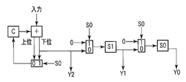
- FIG. 5 shows a 3-NAF conversion device which is a further example of the NAF conversion device of FIG.
- C included in the 3-NAF conversion device corresponds to the 1-bit storage unit 4 in the configuration of FIG.
- Y2, Y1, and Y0 correspond to 3-bit parallel output. + Is a 1-bit adder and corresponds to the element of the updating means 2 in FIG.
- the configuration in which the least significant bit output is given as the clear input of the w-1 bit shift register is the configuration in which Y0, which is part of the parallel output, is given as the selection signal S0 of each of the two selectors in FIG.
- Y0 which is part of the parallel output
- the initial value of C and S0 is 0.
- S0 is 1
- the next value of C is the lower bit of input + C
- the next value of S1 and S0 is 0,
- Y2 is the lower bit of input + C
- Y1 is S1
- Y0 is S0, that is, 1.
- S1 is 0, the next value of C is the upper bit of input + C
- the next value of S1 is the lower bit of input + C
- the next value of S0 is S1
- Y2 is input + C
- Y1 is S1
- Y0 is S0, that is, 0.
- FIG. 6 shows an actual conversion example of this 3-NAF conversion device.
- FIG. 6 is in a timing chart format, and various values are updated each time a clock is input.
- clk is a clock
- start is a start signal
- in is an input
- c is a 1-bit storage means 4
- s is a 2-bit shift register 3
- out is a 3-bit parallel output.
- FIG. 7 shows a 4-NAF conversion device that is a further example of the NAF conversion device of FIG.
- C included in the 4-NAF converter corresponds to the 1-bit storage unit 4 in the configuration of FIG.
- Y3, Y2, Y1, and Y0 correspond to 4-bit parallel output. + Is a 1-bit adder, which is an element of the updating means 2 in FIG.
- S is the least significant bit that changes with k.
- the output is Y3 and Y2 for 2-NAF, Y3, Y2, Y1 for 3-NAF, and Y4, Y3, Y2, Y1, Y0 for 4-NAF.
- the calculation itself is slowed down by reducing w, but the memory can be saved.
- increasing w increases calculation speed but increases memory consumption.
- the calculation can be speeded up by reducing w when the memory is low and increasing w when the memory is high.
- power can be saved by reducing w and stopping power supply to unnecessary registers.
- the 2-NAF conversion device will be described from another viewpoint. That is, the 2-NAF conversion device according to this embodiment will be described in the form of a state transition table as shown in FIG.
- s is the current state (possible states are 3 states), in is a 1-bit input, s' is the next state, and out is an output.
- the state transitions to s' determined by s and in, and the output out is output.
- the state transitions to the first state and 1 is output, and when the input is 1, the state transitions to the third state and ⁇ 1 is output.
- states are circled and correspond to s in the state transition table. There are three states. Number / number means that when the left number is in and the right number is out and the left number is input, the right number is output.
- FIG. 10 like this is a rewrite of the state transition table of FIG. 9 into a state transition diagram.
- the initial state is state 0.
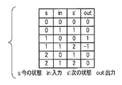
- the above-described 3-NAF conversion device will be described from another viewpoint. That is, the 3-NAF conversion device according to the present embodiment will be described according to the format of the state transition table as shown in FIG.
- the possible values for state s have increased from 0 to 4 to 5 states, and since the output is 3-NAF, there are five ways of -3, -1, 0, 1, 3.
- the state transitions to the first state and 1 is output, and when the input is 1, the state transitions to the 5th state and -3 is output.
- the fourth state when the input is 0, the state transitions to the first state and 3 is output, and when the input is 1, the state transitions to the 5th state and ⁇ 1 is output.
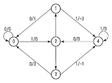
- FIG. 12 shows the state transition table of FIG. 11 rewritten into the state transition diagram, which is the same as FIG.
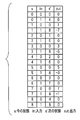
- the above-described 4-NAF conversion device will be described from another viewpoint. That is, the 4-NAF conversion device according to the present embodiment will be described according to the format of the state transition table as shown in FIG. The possible values for state s have increased from 0 to 9 states. Since the output is 4-NAF, there are nine outputs of -7, -5, -3, -1, 0, 1, 3, 5, and 7.
- the state transitions to the first state and outputs 1 when the input is 0, the state transitions to the first state and outputs 1, and when the input is 1, the state transitions to the 9th state and outputs -7.
- the fourth state when the input is 0, the state transitions to the first state and 3 is output, and when the input is 1, the state transitions to the 9th state and ⁇ 5 is output.
- the state transitions to the first state and 5 when the input is 0, the state transitions to the first state and 5 is output, and when the input is 1, the state transitions to the 9th state and -3 is output.
- the state transitions to the fourth state and outputs when the input is 0, the state transitions to the fourth state and outputs 0, and when the input is 1, the state transitions to the 8th state and outputs 0.
- the eighth state when the input is 0, the state transitions to the first state and 7 is output, and when the input is 1, the state transitions to the 9th state and ⁇ 1 is output.
- Fig. 14 shows the 5-NAF converter.
- the state transition table is the same as that described in FIG.
- the value that can be taken as the state s has increased from 0 to 17 states. In general, in the case of w-NAF, it takes 2 ⁇ (w-1) +1 state.
- the above-described embodiment can be realized by a sequential circuit, but can be realized as a synchronous circuit or an asynchronous circuit.
- New crypto attack methods such as side channel attacks have appeared. According to the embodiment described above, it is possible to prevent a side channel attack by changing w during the scalar multiplication of elliptic curve cryptography. w can be changed when the shift register is zero. That is, it is when a value other than 0 is output immediately before.
- the present invention is not limited to the above-described embodiment as it is, and can be embodied by modifying constituent elements without departing from the scope of the invention in the implementation stage.
- various inventions can be formed by appropriately combining a plurality of components disclosed in the embodiment. For example, some components may be deleted from all the components shown in the embodiment.
- constituent elements over different embodiments may be appropriately combined.
Landscapes
- Engineering & Computer Science (AREA)
- Theoretical Computer Science (AREA)
- Physics & Mathematics (AREA)
- General Physics & Mathematics (AREA)
- Computational Mathematics (AREA)
- Mathematical Analysis (AREA)
- Mathematical Optimization (AREA)
- Pure & Applied Mathematics (AREA)
- Computing Systems (AREA)
- General Engineering & Computer Science (AREA)
- Compression, Expansion, Code Conversion, And Decoders (AREA)
- Image Processing (AREA)
Abstract
回路規模が小さくスケーラブルなw-NAF変換装置を提供する。整数の2進表現をw-NAF表現された冗長2進表現に変換するNAF変換装置であって、前記整数の2進表現を下位から1ビットずつ受け付ける受付手段と、1ビットで表現される状態の値を記憶する記憶手段と、w-1ビットで表現される状態の値を記憶するシフトレジスタと、前記受付手段が受け付けた1ビットの値と、前記記憶手段の状態の値と、前記w-1ビットのシフトレジスタの状態の値を参照し、次の時刻における前記記憶手段の状態と前記w-1ビットのシフトレジスタの状態とを決定し、現時刻におけるwビットのパラレル出力を決定する更新手段と、を具備する。
Description
本発明は整数の2進表現を冗長2進表現に変換するNAF変換装置に関する。
乗数を冗長2進表現に変換してから乗算することで乗算を効率化できることについては、例えばBoothの方法として1950年代には既に知られている(例えば非特許文献1、非特許文献2を参照)。最近では、暗号処理の高速化という文脈で冗長2進表現の1種であるNAFが使われることが多い(例えば非特許文献3、非特許文献2を参照)。
NAFについては、例えば非特許文献2の第98頁に説明されている。NAFとは、冗長2進表現の1種であり、整数kは唯一の対応するNAF表現NAF(k)をもつ。NAF(k)の非零の桁の数は任意の冗長2進表現の中でも最小であることが証明されている。非零の桁の数の平均は1/3である。
通常の2進表現では、各桁に0または1の2種類の数字が現れるが、NAFでは-1,0,1の数字が現れるという違いがある。
NAF表現では、引き続く2つの桁の少なくとも一方は0であるという特徴があり、密度が低い理由にもなっている。また、Non-adjacent formという名前の由来でもある。
例として、2進数11011(10進では59=32+16+8+2+1)をNAFに変換すると1000-10-1(64-4-1=59)になる。
4ビット以下の2進数をNAFに変換した例を表1に示す。
整数kをNAF表現NAF(k)に変換するアルゴリズムはいくつも知られている。例えば、非特許文献4の第39頁(表3.2)、非特許文献3の第98頁(アルゴリズム3.30)、非特許文献2の第151(アルゴリズム9.14)に記載されている。
NAFの拡張としてw-NAFがある(例えば非特許文献3の第99頁参照)。
w-NAFと通常のNAFの違いは、w-NAFでは各桁に使える数字がもっと多くなっていることである。3-NAFであれば-3,-1,0,1,3の5種類を使用できる。上記のNAFは2-NAFと考えることができる。
以下、表2および表3にw-NAFの特徴を示す。
表2は、各NAFで使う数字を一覧にしたものである。
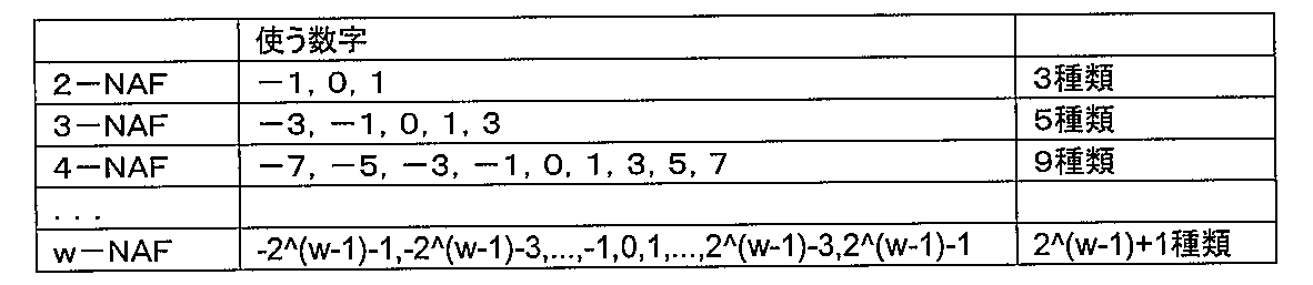
但し、「^」はべき(冪)であり、例えば2^wは2のw乗を意味する。
表3は、各NAFの非零の桁の密度を一覧にしたものである。
w-NAFでは、引き続くw個の桁の内、非零である桁は多くても1つであるという特徴がある。密度が低い方が処理する桁が少なくなるのでクロック数は少なくなるが、事前準備が多くなるのでトレードオフがある。
w-NAFの変換アルゴリズムについては、非特許文献3の第100頁(アルゴリズム3.35)、非特許文献2の第153頁(アルゴリズム9.20)がある。
従来のNAF変換アルゴリズムについて検討する。
非特許文献3のアルゴリズム3.35や、非特許文献2のアルゴリズム9.20は、任意のwに対して適用できるというスケーラビリティの高さが特長であるが、反面、以下のような問題点がある。
・逐次的にkを入力することができない。つまり最初にkを読み込んでおかなければならない。これはkそのものを変更するからである。
・kに対する変更は多倍長演算なので、回路規模が大きくなったり、1桁を求めるのに必要なクロック数が多くなる。
非特許文献4の表3.2について、非特許文献4にはNAF変換であるという記述はないが、結果として出力されるものはNAF変換になっている。このアルゴリズムは上の2つのアルゴリズムのもつ欠点を持たない。つまり、逐次的にkを処理できるし、多倍長演算も不要である。ただし、w=2の場合にしか適用できないのでスケーラビリティがないという問題がある。非特許文献2のアルゴリズム9.14も同じ特長と欠点をもつ。
A.D.Booth, "A signed binary multiplication technique", Quart. J. Mech. Appl. Math., 4, 2, 236-240, 1951.
"Handbook of Elliptic and Hyperelliptic Curve Cryptography", CRC, 2006
"Guide to Elliptic Curve Cryptography", Springer, 2003
「算術演算のVLSIアルゴリズム」コロナ社,2005
上述したように、既に知られているNAF変換アルゴリズムには、スケーラビリティと回路規模が両立しないという問題点がある。
本発明はかかる事情を考慮してなされたものであり、回路規模が小さくスケーラブルなw-NAF変換装置を提供することを目的とする。
本発明の一観点に係るNAF変換装置は、整数の2進表現をw-NAF表現された冗長2進表現に変換するNAF変換装置であって、前記整数の2進表現を下位から1ビットずつ受け付ける受付手段と、1ビットで表現される状態の値を記憶する記憶手段と、w-1ビットで表現される状態の値を記憶するシフトレジスタと、前記受付手段が受け付けた1ビットの値と、前記記憶手段の状態の値と、前記w-1ビットのシフトレジスタの状態の値を参照し、次の時刻における前記記憶手段の状態と前記w-1ビットのシフトレジスタの状態とを決定し、現時刻におけるwビットのパラレル出力を決定する更新手段と、を具備することを特徴とする。
本発明によれば、回路規模が小さくスケーラブルなw-NAF変換装置を提供できる。特に、任意のwについて異なる部分がほとんどない(シフトレジスタの長さだけ)ので、動的にwを変更するといったことも可能である。また、回路規模は知られている2-NAF専用の変換アルゴリズムよりも小型であり、さらには公知のw-NAF変換アルゴリズムと較べても小型である。
以下、図面を参照しながら本発明の実施形態を説明する。
図1は、本発明の実施形態に係るNAF変換装置の機能構成を示すブロック図である。本装置は、1ビットシリアル入力を受け付ける受付手段1と、受付手段1に接続される更新手段2と、更新手段2に接続され、w-NAF表現されたwビットの値をパラレル出力するw-1ビットシフトレジスタ3と、更新手段2に接続される1ビット記憶手段4とを有する。なお、NAF変換装置がハードウェアで構成される場合は、受付手段1は独立して設けられる必要はなく、信号線と更新手段とが接続される接続部分が該当することになる。
1ビット記憶手段4とw-1ビットシフトレジスタ3の初期値は0とする。
本実施形態に係るNAF変換装置においては、w-NAF表現に変換すべき整数の2進表現を下位ビットから順にクロックに合わせて1ビットずつ受付手段1が受け付ける。この受け付けた値を1ビットシリアル入力という。1ビット記憶手段4とw-1ビットシフトレジスタ3の内容はクロック毎に、つまり1ビット入力される毎に更新手段2によって新たな内容に置き換えられる。
更新手段2は更新前の1ビット記憶手段4とw-1ビットシフトレジスタ3の内容および1ビットシリアル入力に応じて、1ビット記憶手段4とw-1ビットシフトレジスタ3の新たな内容を計算する。また更新手段2はwビットのパラレル出力を決定する。つまり、クロック毎にwビットの変換結果が出力される。この際、有効な出力はw-1クロック後から出力される。なお、最下位ビット出力の値“1”は、w-1ビットシフトレジスタ3をクリアするトリガーのクリア入力として、w-1ビットシフトレジスタ3に与えられる。最下位ビット出力の値“1”がw-1ビットシフトレジスタ2に与えられると、w-1ビットシフトレジスタ2の値はクリアされる。
図2を参照して、図1のNAF変換装置をさらに具体化した2-NAF変換装置を説明する。図2に示すように2-NAF変換装置が有するCは図1の構成における1ビット記憶手段4に対応する。同様に、S0は1ビットのシフトレジスタ3(w=2なのでw-1=1ビット)に対応する。Y1とY0は2ビットのパラレル出力に対応する。+は1ビットの加算器であり、図1の更新手段2の要素に対応する。
特別な記号を図3で説明する。セレクタを図3のように記述することにする。つまり選択信号Sが1のとき出力はC=Aであり、Sが0のとき出力はC=Bとなる。
図1において、最下位ビット出力がw-1ビットシフトレジスタのクリア入力として与えられる構成は、図2において、パラレル出力の一部であるY0がセレクタの選択信号S0として与えられる構成に対応する。
CとS0の初期値は0である。S0が1のとき、Cの次の値は入力+Cの下位ビットであり、S0の次の値は0であり、Y1は入力+Cの下位ビットであり、Y0はS0つまり1となる。一方、S0が0のとき、Cの次の値は入力+Cの上位ビットであり、S0の次の値は入力+Cの下位ビットであり、Y1は入力+Cの下位ビットであり、Y0はS0つまり0となる。なお、次のクロックのタイミングでY1の値がS0に書き込まれる。
図4を参照して、この2-NAF変換装置の実際の変換例を示す。図4はタイミングチャートの形式になっており、クロックが入るたびに色々な値が更新されている。図4においてclkはクロック、startは開始信号、inは入力、cは1ビット記憶手段4、sは1ビットシフトレジスタ3、outは2ビットパラレル出力である。
2進数111011(10進では59=32+16+8+2+1)を入力した例を示す。inの行を見ると111011がクロック毎に下位から順に入力されていることが分かる。出力は入力より1クロック遅れている。
出力outの読み方は、「00」または「10」のとき「0」であり、「01」のとき「1」であり、「11」のとき「-1」である。
上記のように0を表現する複数の出力があるが、全て偶数であり、最下位ビットが0のときは出力を0とみなすだけでよい。また、出力が0以外のときは、2ビットの2の補数表現になっていることに注意する。一般にw-NAFの場合は、出力の最下位ビットが0なら0、1ならwビットの2の補数表現となる。出力の最下位ビット以外を最下位ビットとANDをとることできれいな0を出力することもできる。結果も下位から出力される。図4によれば、下位から順に-10-10001と出力されていることが分かる。これは、上位から読むと1000-10-1であり、64-4-1=59なので、元の2進数と同じ数を表現していることが分かる。元の2進数で非零の(1の)ビットは5個であるが、NAF変換後は3個と非零の桁の数が減っている。NAF変換では、出力のビット数は、最大で元のビット数+1になることがあり、この例もそのようになっている。
図5は図1のNAF変換装置をさらに別の例として具体化した3-NAFの変換装置を示している。図5に示すように3-NAF変換装置が有するCは図1の構成における1ビット記憶手段4に対応する。同様に、S1とS0は2ビットのシフトレジスタ3(w=3なのでw-1=2ビット)に対応する。Y2とY1とY0は3ビットのパラレル出力に対応する。+は1ビットの加算器であり、図1の更新手段2の要素に対応する。図1において、最下位ビット出力がw-1ビットシフトレジスタのクリア入力として与えられる構成は、図5において、パラレル出力の一部であるY0が2つのセレクタのそれぞれの選択信号S0として与えられる構成に対応する。
図2の2-NAF変換装置と図5の3-NAFの変換装置とを較べると、Y2とS1が増えただけである。動作は2-NAF変換装置と同様である。
CとS0の初期値は0である。S0が1のとき、Cの次の値は入力+Cの下位ビットであり、S1とS0の次の値は0であり、Y2は入力+Cの下位ビットであり、Y1はS1であり、Y0はS0つまり1となる。一方、S1が0のとき、Cの次の値は入力+Cの上位ビットであり、S1の次の値は入力+Cの下位ビットであり、S0の次の値はS1であり、Y2は入力+Cの下位ビットであり、Y1はS1であり、Y0はS0つまり0となる。
図6を参照して、この3-NAF変換装置の実際の変換例を示す。図6はタイミングチャートの形式になっており、クロックが入るたびに色々な値が更新されている。図6において、clkはクロック、startは開始信号、inは入力、cは1ビット記憶手段4、sは2ビットシフトレジスタ3、outは3ビットパラレル出力である。
2進数111011(10進では59=32+16+8+2+1)を入力した例を示す。inの行を見ると111011がクロック毎に下位から順に入力されていることが分かる。出力は入力より2クロック遅れている。出力outの読み方は、「000」,「010」,「100」,「110」のとき、「0」であり、「001」のとき「1」であり、「011」のとき「3」であり、「101」のとき「-3」であり、「111」のとき「-1」である。
上記のように0を表現する複数の出力があるが、全て偶数であり、最下位ビットが0のときは出力を0とみなすだけでよい。また、出力が0以外のときは、3ビットの2の補数表現になっていることに注意する。結果も下位から出力される。下位から順に300-1001と出力されていることが分かる。これは、上位から読むと100-1003であり、64-8+3=59なので、元の2進数と同じ数を表現していることが分かる。NAF変換では、出力のビット数は、最大で元のビット数+1になることがあり、この例もそのようになっている。
図7は図1のNAF変換装置をさらに別の例として具体化した4-NAFの変換装置である。図7に示すように、4-NAFの変換装置が有するCは図1の構成における1ビット記憶手段4に対応する。同様に、S2とS1とS0は3ビットのシフトレジスタ3(w=4なのでw-1=3ビット)に対応する。Y3とY2とY1とY0は4ビットのパラレル出力に対応する。+は1ビットの加算器であり、図1の更新手段2の要素である。
図2の2-NAF変換装置や図5の3-NAF変換装置と図7の4-NAF変換装置とを見比べてみると、シフトレジスタ3と出力が増えただけで同じ構造をもつことが分かる。
図8を参照して、kを可変とするk-NAF変換装置の例を示す。この例ではkの値として2,3,4を選択できる。図8においてk-NAF変換装置のCは図1に示した構成における1ビット記憶手段4に対応する。S2とS1とS0は図1の構成における3ビットのシフトレジスタ3(w=4なのでw-1=3ビット)に対応する。Y3とY2とY1とY0は4ビットのパラレル出力に対応する。+は1ビットの加算器である。
Sはkによって変わる最下位ビットである。k=2、つまりこの装置を2-NAF変換装置として動作させるには、最下位ビットSとしてS2を採用すればよく、同様に3-NAF変換装置として動作させるためには、最下位ビットSとしてS1を採用すればよく、4-NAF変換装置の場合の最下位ビットはS=S0とすればよい。このとき、出力は2-NAFのときはY3とY2とし、3-NAFのときはY3,Y2,Y1とし、4-NAFのときはY4,Y3,Y2,Y1,Y0とする。
携帯機器のようにメモリが限られているような場面では、wを小さくすることで計算自体は遅くなるが、メモリを節約することができる。一般にwを大きくすることで計算は速くなるがメモリ消費量が増える。例えばメモリの空きが少ないときはwを小さくし、メモリの空きが多いときはwを大きくすることで計算を速くすることができる。また、wを小さくし不要なレジスタへの給電を止めることで、電力を節約できる。
図9を参照して、上述した2-NAF変換装置を他の観点から説明する。すなわち、図9のような状態遷移表の形式で本実施形態に係る2-NAF変換装置を説明する。図9において、sは今の状態(取りうる状態は3状態である)、inは1ビットの入力、s’は次の状態、outは出力である。初期状態はs=0である。入力inが1ビットずつ入るたびにsとinで決まるs’に状態遷移し、出力outを出力する。
第1の状態において、入力が0のときは、第1の状態に状態遷移し、0を出力し、入力が1のときは、第2の状態に状態遷移し、0を出力する。第2の状態において、入力が0のときは、第1の状態に状態遷移し、1を出力し、入力が1のときは、第3の状態に状態遷移し、-1を出力する。第3の状態において、入力が0のときは、第2の状態に状態遷移し、0を出力し、入力が1のときは、第3の状態に状態遷移し、0を出力する。このようにして整数の2進表現を下位から1ビットずつ入力すると2-NAF表現された冗長2進表現を2ビットずつ出力する。
図10を参照して、2-NAF変換装置をさらに説明する。図10において、丸で囲まれているのが状態であり、状態遷移表のsと対応する。3つの状態がある。数字/数字は、左の数字がin、右の数字がoutで、左の数字を入力したときに、右の数字を出力することを意味する。このような図10は、図9の状態遷移表を状態遷移図の形に書き直したものである。初期状態は状態0である。
図11を参照して、上述した3-NAF変換装置を他の観点から説明する。すなわち、図11のような状態遷移表の形式に沿って本実施形態に係る3-NAF変換装置を説明する。状態sとして取りうる値が0から4の5状態に増えており、出力は、3-NAFなので-3,-1,0,1,3の5通りになっている。
第1の状態において、入力が0のときは、第1の状態に状態遷移し、0を出力し、入力が1のときは、第3の状態に状態遷移し、0を出力する。第2の状態において、入力が0のときは、第1の状態に状態遷移し、1を出力し、入力が1のときは、第5の状態に状態遷移し、-3を出力する。第3の状態において、入力が0のときは、第2の状態に状態遷移し、0を出力し、入力が1のときは、第4の状態に状態遷移し、0を出力する。第4の状態において、入力が0のときは、第1の状態に状態遷移し、3を出力し、入力が1のときは、第5の状態に状態遷移し、-1を出力する。第5の状態において、入力が0のときは、第3の状態に状態遷移し、0を出力し、入力が1のときは、第5の状態に状態遷移し、0を出力する。こうして、整数の2進表現を下位から1ビットずつ入力すると、3-NAF表現された冗長2進表現を3ビットずつ出力する。
図12は、図11の状態遷移表を状態遷移図に書き直したものであり、図10と同様である。
図13を参照して、上述した4-NAF変換装置を他の観点から説明する。すなわち、図13のような状態遷移表の形式に沿って本実施形態に係る4-NAF変換装置を説明する。状態sとして取りうる値が0から8の9状態に増えている。出力は、4-NAFであので-7,-5,-3,-1,0,1,3,5,7の9種類である。
第1の状態において、入力が0のときは、第1の状態に状態遷移し、0を出力し、入力が1のときは、第5の状態に状態遷移し、0を出力する。第2の状態において、入力が0のときは、第1の状態に状態遷移し、1を出力し、入力が1のときは、第9の状態に状態遷移し、-7を出力する。第3の状態において、入力が0のときは、第2の状態に状態遷移し、0を出力し、入力が1のときは、第6の状態に状態遷移し、0を出力する。第4の状態において、入力が0のときは、第1の状態に状態遷移し、3を出力し、入力が1のときは、第9の状態に状態遷移し、-5を出力する。第5の状態において、入力が0のときは、第3の状態に状態遷移し、0を出力し、入力が1のときは、第7の状態に状態遷移し、0を出力する。第6の状態において、入力が0のときは、第1の状態に状態遷移し、5を出力し、入力が1のときは、第9の状態に状態遷移し、-3を出力する。第7の状態において、入力が0のときは、第4の状態に状態遷移し、0を出力し、入力が1のときは、第8の状態に状態遷移し、0を出力する。第8の状態において、入力が0のときは、第1の状態に状態遷移し、7を出力し、入力が1のときは、第9の状態に状態遷移し、-1を出力する。第9の状態において、入力が0のときは、第5の状態に状態遷移し、0を出力し、入力が1のときは、第9の状態に状態遷移し、0を出力する。こうして整数の2進表現を下位から1ビットずつ入力すると4-NAF表現された冗長2進表現を4ビットずつ出力する。
図14によって5-NAF変換装置を示す。状態遷移表については図9の説明と同様である。状態sとして取りうる値が0から16の17状態に増えている。一般に、w-NAFの場合は、2^(w-1)+1状態を取る。
上述した実施形態は順序回路によって実現できるが、同期回路としても非同期回路としても実現可能である。
サイドチャネル攻撃のような新たな暗号攻撃法が登場している。以上説明した実施形態によれば、楕円曲線暗号のスカラー倍の途中でwを変化させることで、サイドチャネル攻撃を防ぐことが可能になる。wを変更できるのは、シフトレジスタが0の場合である。つまり、直前に0以外の値を出力したときである。
なお、本発明は上記実施形態そのままに限定されるものではなく、実施段階ではその要旨を逸脱しない範囲で構成要素を変形して具体化できる。また、上記実施形態に開示されている複数の構成要素の適宜な組み合わせにより、種々の発明を形成できる。例えば、実施形態に示される全構成要素から幾つかの構成要素を削除してもよい。さらに、異なる実施形態にわたる構成要素を適宜組み合わせてもよい。
1…受付手段;
2…更新手段;
3…w-1ビットシフトレジスタ;
4…1ビット記憶手段
2…更新手段;
3…w-1ビットシフトレジスタ;
4…1ビット記憶手段
Claims (10)
- 整数の2進表現をw-NAF表現された冗長2進表現に変換するNAF変換装置であって、
前記整数の2進表現を下位から1ビットずつ受け付ける受付手段と、
1ビットで表現される状態の値を記憶する記憶手段と、
w-1ビットで表現される状態の値を記憶するシフトレジスタと、
前記受付手段が受け付けた1ビットの値と、前記記憶手段の状態の値と、前記w-1ビットのシフトレジスタの状態の値を参照し、次の時刻における前記記憶手段の状態と前記w-1ビットのシフトレジスタの状態とを決定し、現時刻におけるwビットのパラレル出力を決定する更新手段と、
を具備することを特徴とするNAF変換装置。 - 前記更新手段は、
前記次の時刻における前記記憶手段の状態を、
前記現時刻における前記w-1ビットのシフトレジスタの最下位ビットが1のときは、前記シリアル入力から入力された1ビットと前記現時刻の記憶手段の状態との和の下位1ビットとし、前記現時刻における前記w-1ビットのシフトレジスタの最上位ビットが0のときは、前記和の上位1ビットとし、
前記次の時刻における前記w-1ビットのシフトレジスタの状態を、
前記現時刻における前記w-1ビットのシフトレジスタの最下位ビットが1のときは、w-1ビットの0とし、前記現時刻における前記w-1ビットのシフトレジスタの最下位ビットが0のときは、前記現時刻における該シフトレジスタを下位に向けて1ビットシフトし、該和の下位ビットを最上位ビットとしたw-1ビットの値とし、
前記現時刻におけるパラレル出力を、
前記和の下位ビットを最上位ビットとし、下位w-1ビットが前記w-1ビットのシフトレジスタの値とすることを特徴とする請求項1記載のNAF変換装置。 - 前記w-1シフトレジスタの最下位ビットに代えて、下位(w-k)ビットを使い、該パラレル出力の上位kビットを出力とすることを特徴とする請求項1記載のNAF変換装置。
- CPUパワーおよびメモリ量を含む使用可能なリソースに応じた小さな値に前記kを設定することを特徴とする請求項3記載のNAF変換装置。
- NAF変換の途中でkの値を2からwの間で変化させることを特徴とする請求項3記載のNAF変換装置。
- 前記1ビットの記憶手段、前記w-1ビットのシフトレジスタ、前記更新手段が同期回路であることを特徴とする請求項1記載のNAF変換装置。
- 前記1ビットの記憶手段、前記w-1ビットのシフトレジスタ、前記更新手段が非同期回路であることを特徴とする請求項1記載のNAF変換装置。
- 1ビットシリアル入力と、
2ビットパラレル出力と、
3つの状態を記憶する記憶手段と、
第1の状態において、
入力が0のときは、第1の状態に状態遷移し、0を出力し、
入力が1のときは、第2の状態に状態遷移し、0を出力し、
第2の状態において、
入力が0のときは、第1の状態に状態遷移し、1を出力し、
入力が1のときは、第3の状態に状態遷移し、-1を出力し、
第3の状態において、
入力が0のときは、第2の状態に状態遷移し、0を出力し、
入力が1のときは、第3の状態に状態遷移し、0を出力する更新手段と、
を具備し、
整数の2進表現を下位から1ビットずつ前記シリアル入力から入力すると2-NAF表現された冗長2進表現を2ビットずつ前記パラレル出力から出力する2-NAF変換装置。 - 1ビットシリアル入力と、
3ビットパラレル出力と、
5つの状態を記憶する記憶手段と、
第1の状態において、
入力が0のときは、第1の状態に状態遷移し、0を出力し、
入力が1のときは、第3の状態に状態遷移し、0を出力し、
第2の状態において、
入力が0のときは、第1の状態に状態遷移し、1を出力し、
入力が1のときは、第5の状態に状態遷移し、-3を出力し、
第3の状態において、
入力が0のときは、第2の状態に状態遷移し、0を出力し、
入力が1のときは、第4の状態に状態遷移し、0を出力し、
第4の状態において、
入力が0のときは、第1の状態に状態遷移し、3を出力し、
入力が1のときは、第5の状態に状態遷移し、-1を出力し、
第5の状態において、
入力が0のときは、第3の状態に状態遷移し、0を出力し、
入力が1のときは、第5の状態に状態遷移し、0を出力する更新手段と、
を具備し、
整数の2進表現を下位から1ビットずつ前記シリアル入力から入力すると3-NAF表現された冗長2進表現を3ビットずつ前記パラレル出力から出力することを特徴とする3-NAF変換装置。 - 1ビットシリアル入力と、
4ビットパラレル出力と、
9つの状態を記憶する記憶手段と、
第1の状態において、
入力が0のときは、第1の状態に状態遷移し、0を出力し、
入力が1のときは、第5の状態に状態遷移し、0を出力し、
第2の状態において、
入力が0のときは、第1の状態に状態遷移し、1を出力し、
入力が1のときは、第9の状態に状態遷移し、-7を出力し、
第3の状態において、
入力が0のときは、第2の状態に状態遷移し、0を出力し、
入力が1のときは、第6の状態に状態遷移し、0を出力し、
第4の状態において、
入力が0のときは、第1の状態に状態遷移し、3を出力し、
入力が1のときは、第9の状態に状態遷移し、-5を出力し、
第5の状態において、
入力が0のときは、第3の状態に状態遷移し、0を出力し、
入力が1のときは、第7の状態に状態遷移し、0を出力し、
第6の状態において、
入力が0のときは、第1の状態に状態遷移し、5を出力し、
入力が1のときは、第9の状態に状態遷移し、-3を出力し、
第7の状態において、
入力が0のときは、第4の状態に状態遷移し、0を出力し、
入力が1のときは、第8の状態に状態遷移し、0を出力し、
第8の状態において、
入力が0のときは、第1の状態に状態遷移し、7を出力し、
入力が1のときは、第9の状態に状態遷移し、-1を出力し、
第9の状態において、
入力が0のときは、第5の状態に状態遷移し、0を出力し、
入力が1のときは、第9の状態に状態遷移し、0を出力する更新手段と、
を具備し、
整数の2進表現を下位から1ビットずつ前記シリアル入力から入力すると、4-NAF表現された冗長2進表現を4ビットずつ前記パラレル出力から出力することを特徴とする4-NAF変換装置。
Priority Applications (1)
| Application Number | Priority Date | Filing Date | Title |
|---|---|---|---|
| US13/183,625 US8918441B2 (en) | 2009-01-15 | 2011-07-15 | NAF conversion apparatus |
Applications Claiming Priority (2)
| Application Number | Priority Date | Filing Date | Title |
|---|---|---|---|
| JP2009006797A JP5225115B2 (ja) | 2009-01-15 | 2009-01-15 | Naf変換装置 |
| JP2009-006797 | 2009-01-15 |
Related Child Applications (1)
| Application Number | Title | Priority Date | Filing Date |
|---|---|---|---|
| US13/183,625 Continuation US8918441B2 (en) | 2009-01-15 | 2011-07-15 | NAF conversion apparatus |
Publications (1)
| Publication Number | Publication Date |
|---|---|
| WO2010082629A1 true WO2010082629A1 (ja) | 2010-07-22 |
Family
ID=42339882
Family Applications (1)
| Application Number | Title | Priority Date | Filing Date |
|---|---|---|---|
| PCT/JP2010/050420 Ceased WO2010082629A1 (ja) | 2009-01-15 | 2010-01-15 | Naf変換装置 |
Country Status (3)
| Country | Link |
|---|---|
| US (1) | US8918441B2 (ja) |
| JP (1) | JP5225115B2 (ja) |
| WO (1) | WO2010082629A1 (ja) |
Families Citing this family (3)
| Publication number | Priority date | Publication date | Assignee | Title |
|---|---|---|---|---|
| JP5225115B2 (ja) * | 2009-01-15 | 2013-07-03 | 株式会社東芝 | Naf変換装置 |
| CN105656629B (zh) * | 2014-11-25 | 2018-12-11 | 上海华虹集成电路有限责任公司 | 芯片中安全的非相邻表示型实现方法 |
| WO2018145189A1 (en) * | 2017-02-13 | 2018-08-16 | Infosec Global Inc. | Countermeasures and optimizations in elliptic curve cryptographic schemes |
Citations (4)
| Publication number | Priority date | Publication date | Assignee | Title |
|---|---|---|---|---|
| JPS63311433A (ja) * | 1987-06-12 | 1988-12-20 | Nippon Telegr & Teleph Corp <Ntt> | 2進冗長sd符号変換減算方法及びその実施する回路 |
| JPH01226221A (ja) * | 1988-03-04 | 1989-09-08 | Nec Corp | 数値変換装置 |
| JPH10307705A (ja) * | 1997-05-02 | 1998-11-17 | Fujitsu Ltd | 冗長2進符号変換回路及びこれを用いた乗算回路 |
| WO2006054559A1 (ja) * | 2004-11-22 | 2006-05-26 | Sony Corporation | 暗号処理演算装置 |
Family Cites Families (5)
| Publication number | Priority date | Publication date | Assignee | Title |
|---|---|---|---|---|
| US20020057796A1 (en) * | 1998-12-24 | 2002-05-16 | Lambert Robert J. | Method for accelerating cryptographic operations on elliptic curves |
| FR2820905B1 (fr) * | 2001-02-09 | 2005-02-18 | Gemplus Card Int | Dispositif et procede de traitement de valeurs numeriques, notamment sous forme non-adjacente |
| US7602907B2 (en) * | 2005-07-01 | 2009-10-13 | Microsoft Corporation | Elliptic curve point multiplication |
| JP5225115B2 (ja) * | 2009-01-15 | 2013-07-03 | 株式会社東芝 | Naf変換装置 |
| JP5175983B2 (ja) * | 2009-09-24 | 2013-04-03 | 株式会社東芝 | 演算装置 |
-
2009
- 2009-01-15 JP JP2009006797A patent/JP5225115B2/ja not_active Expired - Fee Related
-
2010
- 2010-01-15 WO PCT/JP2010/050420 patent/WO2010082629A1/ja not_active Ceased
-
2011
- 2011-07-15 US US13/183,625 patent/US8918441B2/en active Active
Patent Citations (4)
| Publication number | Priority date | Publication date | Assignee | Title |
|---|---|---|---|---|
| JPS63311433A (ja) * | 1987-06-12 | 1988-12-20 | Nippon Telegr & Teleph Corp <Ntt> | 2進冗長sd符号変換減算方法及びその実施する回路 |
| JPH01226221A (ja) * | 1988-03-04 | 1989-09-08 | Nec Corp | 数値変換装置 |
| JPH10307705A (ja) * | 1997-05-02 | 1998-11-17 | Fujitsu Ltd | 冗長2進符号変換回路及びこれを用いた乗算回路 |
| WO2006054559A1 (ja) * | 2004-11-22 | 2006-05-26 | Sony Corporation | 暗号処理演算装置 |
Non-Patent Citations (3)
| Title |
|---|
| K.OKEYA, T.TAKAGI: "The Width-w NAF Method Provides Small Memory and Fast Elliptic Scalar Multiplications Secure against Side Channel Attacks", RSA CONFERENCE CRYPTOGRAPHER'S TRACK (CT-RSA 2003), 2003, LNCS 2612, 2003, pages 328 - 343 * |
| MARC JOYE ET AL.: "Optimal Left-to- Right Binary Signed-Digit Recoding", IEEE TRANSACTIONS ON COMPUTERS, vol. 49, no. 7, July 2000 (2000-07-01), pages 740 - 748 * |
| TSUYOSHI TKAGI ET AL.: "Radix-r Non-Adjacent Form and Its Application to Pairing-Based Cryptosystem", IEICE TRANSACTIONS ON FUNDAMENTALS OF ELECTRONICS, COMMUNICATIONS AND COMPUTER SCIENCES, vol. E89-A, no. 1, January 2006 (2006-01-01), pages 115 - 123 * |
Also Published As
| Publication number | Publication date |
|---|---|
| JP2010165173A (ja) | 2010-07-29 |
| US20110320511A1 (en) | 2011-12-29 |
| US8918441B2 (en) | 2014-12-23 |
| JP5225115B2 (ja) | 2013-07-03 |
Similar Documents
| Publication | Publication Date | Title |
|---|---|---|
| US8504602B2 (en) | Modular multiplication processing apparatus | |
| EP1471420A2 (en) | Montgomery modular multiplier and method thereof using carry save addition | |
| US20040252829A1 (en) | Montgomery modular multiplier and method thereof using carry save addition | |
| CN106484366A (zh) | 一种二元域位宽可变模乘运算器 | |
| KR20220049212A (ko) | 모듈러 연산을 위한 워드 병렬 연산 방법 | |
| US20200097257A1 (en) | Electronic calculating device arranged to calculate the product of integers | |
| JP5225115B2 (ja) | Naf変換装置 | |
| US7307453B1 (en) | Method and system for parallel state machine implementation | |
| US8085931B2 (en) | Computation method, computing device and computer program | |
| JP3003467B2 (ja) | 演算装置 | |
| JP5606516B2 (ja) | Naf変換装置 | |
| JP5175983B2 (ja) | 演算装置 | |
| Wu et al. | Modular multiplier by folding Barrett modular reduction | |
| JP3660075B2 (ja) | 除算装置 | |
| CN102646033B (zh) | 提供了加密和签名功能的rsa算法的实现方法和装置 | |
| CN102270110B (zh) | 一种改进的基16Booth编码器 | |
| Lou et al. | High-speed multiplier block design based on bit-level critical path optimization | |
| JP2004166274A (ja) | 有限体での基底変換方法及び基底変換装置 | |
| US7472154B2 (en) | Multiplication remainder calculator | |
| KR102856644B1 (ko) | 싸인 비트 감산기 및 비트 최적화를 적용한 프리 엠퍼시스 회로 | |
| JP2015114434A (ja) | ストリーム暗号の暗号化装置、ストリーム暗号の復号化装置、ストリーム暗号の暗号化方法、ストリーム暗号の復号化方法およびプログラム | |
| WO2025173167A1 (ja) | 演算装置及び演算方法 | |
| Peijun et al. | A 1024-bit RSA cryptosystem hardware design based on modified Montgomery's algorithm | |
| JP4408727B2 (ja) | ディジタル回路 | |
| JP2000165204A (ja) | Iir形デジタルローパスフィルタ |
Legal Events
| Date | Code | Title | Description |
|---|---|---|---|
| 121 | Ep: the epo has been informed by wipo that ep was designated in this application |
Ref document number: 10731298 Country of ref document: EP Kind code of ref document: A1 |
|
| NENP | Non-entry into the national phase |
Ref country code: DE |
|
| 122 | Ep: pct application non-entry in european phase |
Ref document number: 10731298 Country of ref document: EP Kind code of ref document: A1 |