WO2010082525A1 - 絶縁層用樹脂組成物 - Google Patents
絶縁層用樹脂組成物 Download PDFInfo
- Publication number
- WO2010082525A1 WO2010082525A1 PCT/JP2010/050082 JP2010050082W WO2010082525A1 WO 2010082525 A1 WO2010082525 A1 WO 2010082525A1 JP 2010050082 W JP2010050082 W JP 2010050082W WO 2010082525 A1 WO2010082525 A1 WO 2010082525A1
- Authority
- WO
- WIPO (PCT)
- Prior art keywords
- group
- insulating layer
- repeating unit
- film transistor
- organic
- Prior art date
- Legal status (The legal status is an assumption and is not a legal conclusion. Google has not performed a legal analysis and makes no representation as to the accuracy of the status listed.)
- Ceased
Links
Images

Classifications
-
- C—CHEMISTRY; METALLURGY
- C08—ORGANIC MACROMOLECULAR COMPOUNDS; THEIR PREPARATION OR CHEMICAL WORKING-UP; COMPOSITIONS BASED THEREON
- C08F—MACROMOLECULAR COMPOUNDS OBTAINED BY REACTIONS ONLY INVOLVING CARBON-TO-CARBON UNSATURATED BONDS
- C08F8/00—Chemical modification by after-treatment
-
- C—CHEMISTRY; METALLURGY
- C08—ORGANIC MACROMOLECULAR COMPOUNDS; THEIR PREPARATION OR CHEMICAL WORKING-UP; COMPOSITIONS BASED THEREON
- C08G—MACROMOLECULAR COMPOUNDS OBTAINED OTHERWISE THAN BY REACTIONS ONLY INVOLVING UNSATURATED CARBON-TO-CARBON BONDS
- C08G18/00—Polymeric products of isocyanates or isothiocyanates
- C08G18/06—Polymeric products of isocyanates or isothiocyanates with compounds having active hydrogen
- C08G18/70—Polymeric products of isocyanates or isothiocyanates with compounds having active hydrogen characterised by the isocyanates or isothiocyanates used
- C08G18/72—Polyisocyanates or polyisothiocyanates
- C08G18/728—Polymerisation products of compounds having carbon-to-carbon unsaturated bonds and having isocyanate or isothiocyanate groups or groups forming isocyanate or isothiocyanate groups
-
- C—CHEMISTRY; METALLURGY
- C08—ORGANIC MACROMOLECULAR COMPOUNDS; THEIR PREPARATION OR CHEMICAL WORKING-UP; COMPOSITIONS BASED THEREON
- C08F—MACROMOLECULAR COMPOUNDS OBTAINED BY REACTIONS ONLY INVOLVING CARBON-TO-CARBON UNSATURATED BONDS
- C08F299/00—Macromolecular compounds obtained by interreacting polymers involving only carbon-to-carbon unsaturated bond reactions, in the absence of non-macromolecular monomers
-
- C—CHEMISTRY; METALLURGY
- C08—ORGANIC MACROMOLECULAR COMPOUNDS; THEIR PREPARATION OR CHEMICAL WORKING-UP; COMPOSITIONS BASED THEREON
- C08G—MACROMOLECULAR COMPOUNDS OBTAINED OTHERWISE THAN BY REACTIONS ONLY INVOLVING UNSATURATED CARBON-TO-CARBON BONDS
- C08G18/00—Polymeric products of isocyanates or isothiocyanates
- C08G18/06—Polymeric products of isocyanates or isothiocyanates with compounds having active hydrogen
- C08G18/70—Polymeric products of isocyanates or isothiocyanates with compounds having active hydrogen characterised by the isocyanates or isothiocyanates used
- C08G18/81—Unsaturated isocyanates or isothiocyanates
- C08G18/8108—Unsaturated isocyanates or isothiocyanates having only one isocyanate or isothiocyanate group
- C08G18/8116—Unsaturated isocyanates or isothiocyanates having only one isocyanate or isothiocyanate group esters of acrylic or alkylacrylic acid having only one isocyanate or isothiocyanate group
-
- H—ELECTRICITY
- H10—SEMICONDUCTOR DEVICES; ELECTRIC SOLID-STATE DEVICES NOT OTHERWISE PROVIDED FOR
- H10K—ORGANIC ELECTRIC SOLID-STATE DEVICES
- H10K10/00—Organic devices specially adapted for rectifying, amplifying, oscillating or switching; Organic capacitors or resistors having potential barriers
- H10K10/40—Organic transistors
- H10K10/46—Field-effect transistors, e.g. organic thin-film transistors [OTFT]
- H10K10/462—Insulated gate field-effect transistors [IGFETs]
- H10K10/464—Lateral top-gate IGFETs comprising only a single gate
-
- H—ELECTRICITY
- H10—SEMICONDUCTOR DEVICES; ELECTRIC SOLID-STATE DEVICES NOT OTHERWISE PROVIDED FOR
- H10K—ORGANIC ELECTRIC SOLID-STATE DEVICES
- H10K10/00—Organic devices specially adapted for rectifying, amplifying, oscillating or switching; Organic capacitors or resistors having potential barriers
- H10K10/40—Organic transistors
- H10K10/46—Field-effect transistors, e.g. organic thin-film transistors [OTFT]
- H10K10/462—Insulated gate field-effect transistors [IGFETs]
- H10K10/466—Lateral bottom-gate IGFETs comprising only a single gate
-
- H—ELECTRICITY
- H10—SEMICONDUCTOR DEVICES; ELECTRIC SOLID-STATE DEVICES NOT OTHERWISE PROVIDED FOR
- H10K—ORGANIC ELECTRIC SOLID-STATE DEVICES
- H10K10/00—Organic devices specially adapted for rectifying, amplifying, oscillating or switching; Organic capacitors or resistors having potential barriers
- H10K10/40—Organic transistors
- H10K10/46—Field-effect transistors, e.g. organic thin-film transistors [OTFT]
- H10K10/462—Insulated gate field-effect transistors [IGFETs]
- H10K10/468—Insulated gate field-effect transistors [IGFETs] characterised by the gate dielectrics
-
- H—ELECTRICITY
- H10—SEMICONDUCTOR DEVICES; ELECTRIC SOLID-STATE DEVICES NOT OTHERWISE PROVIDED FOR
- H10K—ORGANIC ELECTRIC SOLID-STATE DEVICES
- H10K10/00—Organic devices specially adapted for rectifying, amplifying, oscillating or switching; Organic capacitors or resistors having potential barriers
- H10K10/80—Constructional details
- H10K10/88—Passivation; Containers; Encapsulations
-
- H—ELECTRICITY
- H10—SEMICONDUCTOR DEVICES; ELECTRIC SOLID-STATE DEVICES NOT OTHERWISE PROVIDED FOR
- H10P—GENERIC PROCESSES OR APPARATUS FOR THE MANUFACTURE OR TREATMENT OF DEVICES COVERED BY CLASS H10
- H10P14/00—Formation of materials, e.g. in the shape of layers or pillars
- H10P14/60—Formation of materials, e.g. in the shape of layers or pillars of insulating materials
- H10P14/63—Formation of materials, e.g. in the shape of layers or pillars of insulating materials characterised by the formation processes
- H10P14/6326—Deposition processes
- H10P14/6342—Liquid deposition, e.g. spin-coating, sol-gel techniques or spray coating
-
- H—ELECTRICITY
- H10—SEMICONDUCTOR DEVICES; ELECTRIC SOLID-STATE DEVICES NOT OTHERWISE PROVIDED FOR
- H10P—GENERIC PROCESSES OR APPARATUS FOR THE MANUFACTURE OR TREATMENT OF DEVICES COVERED BY CLASS H10
- H10P14/00—Formation of materials, e.g. in the shape of layers or pillars
- H10P14/60—Formation of materials, e.g. in the shape of layers or pillars of insulating materials
- H10P14/68—Organic materials, e.g. photoresists
- H10P14/683—Organic materials, e.g. photoresists carbon-based polymeric organic materials, e.g. polyimides, poly cyclobutene or PVC
-
- H—ELECTRICITY
- H10—SEMICONDUCTOR DEVICES; ELECTRIC SOLID-STATE DEVICES NOT OTHERWISE PROVIDED FOR
- H10P—GENERIC PROCESSES OR APPARATUS FOR THE MANUFACTURE OR TREATMENT OF DEVICES COVERED BY CLASS H10
- H10P14/00—Formation of materials, e.g. in the shape of layers or pillars
- H10P14/60—Formation of materials, e.g. in the shape of layers or pillars of insulating materials
- H10P14/69—Inorganic materials
- H10P14/692—Inorganic materials composed of oxides, glassy oxides or oxide-based glasses
- H10P14/6921—Inorganic materials composed of oxides, glassy oxides or oxide-based glasses containing silicon
- H10P14/69215—Inorganic materials composed of oxides, glassy oxides or oxide-based glasses containing silicon the material being a silicon oxide, e.g. SiO2
Definitions
- the present invention relates to a resin composition for forming an insulating layer, and particularly to a resin composition for forming an insulating layer in an organic thin film transistor.
- Organic field effect transistors can be manufactured at a lower temperature than inorganic semiconductors, so that a plastic substrate or film can be used as a substrate, and an element that is light and difficult to break can be manufactured.
- an element can be manufactured by application of a solution containing an organic material or film formation using a printing method, and thus a large-area element can be manufactured at low cost.
- material characteristics can be easily changed. Therefore, by combining materials having different functions, it is possible to realize flexible functions, elements, and the like that are impossible with inorganic semiconductors.
- the voltage applied to the gate electrode acts on the semiconductor layer through the gate insulating layer to control on / off of the drain current. Therefore, a gate insulating layer is formed between the gate electrode and the semiconductor layer.
- organic semiconductor compounds used in organic field effect transistors are easily affected by the environment such as humidity and oxygen, and the transistor characteristics are likely to deteriorate over time due to humidity, oxygen and the like.
- the organic semiconductor compound is coated and protected by a gate insulating layer.
- a resin composition is used to form an overcoat layer, a gate insulating layer, and the like that cover an organic semiconductor layer.
- the resin composition used to form such an insulating layer and insulating film is referred to as an insulating layer resin composition.
- Insulating layer resin composition includes dielectric breakdown strength when thinned, affinity with organic semiconductor to form good interface with organic semiconductor, flatness of film surface forming interface with semiconductor, etc. Characteristics are required. In addition, when the polymer compound contained in the insulating layer is cross-linked, the electrical characteristics are improved. However, if the resin composition for the insulating layer is treated for a long time at a high temperature for the cross-linking, the organic matter constituting the element deteriorates. As a result, transistor characteristics deteriorate. Therefore, it is preferable that the insulating layer resin composition is crosslinked at a relatively low temperature.
- Patent Document 1 reports a layer containing a fluororesin as a gate insulating layer in an organic field effect transistor.
- a fluororesin as a gate insulating layer
- the present invention solves the above-mentioned conventional problems, and an object of the present invention is to provide an organic thin film transistor insulating layer resin capable of forming an insulating layer having excellent surface adhesion without performing treatment at a high temperature for a long time. It is to provide a composition.
- the present invention firstly includes (A) a polymer compound containing a repeating unit having a photosensitive group bonded via a urea bond or a urethane bond, (B) a curing agent, (C) an organic solvent,
- A a polymer compound containing a repeating unit having a photosensitive group bonded via a urea bond or a urethane bond
- B a curing agent
- C an organic solvent
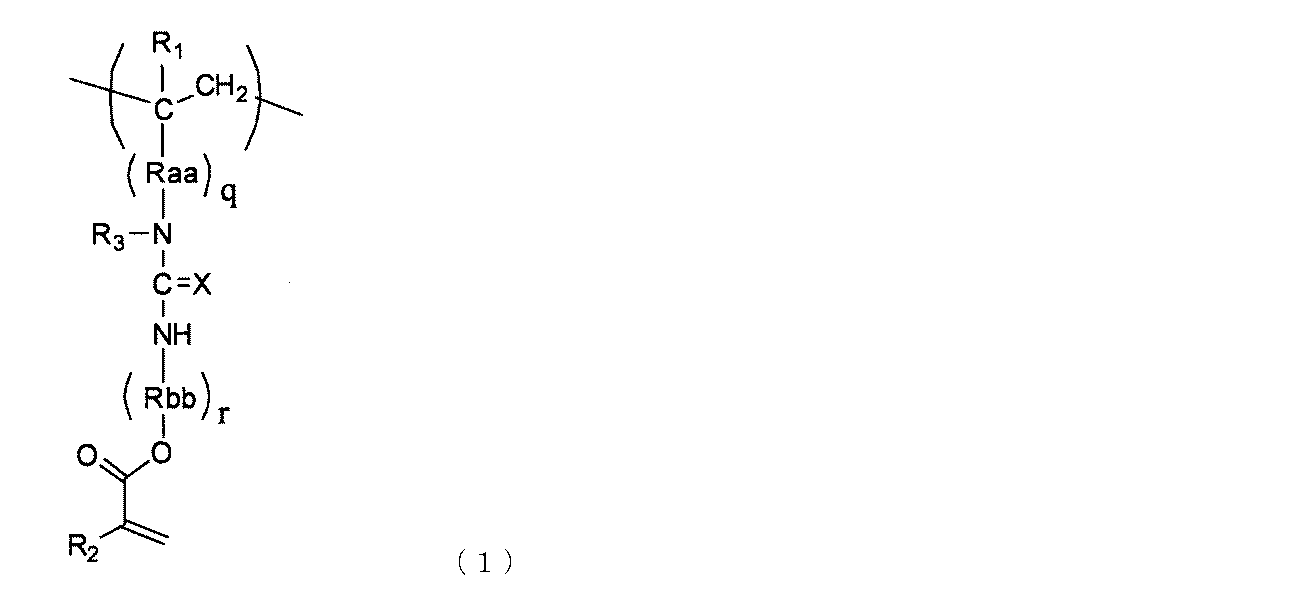
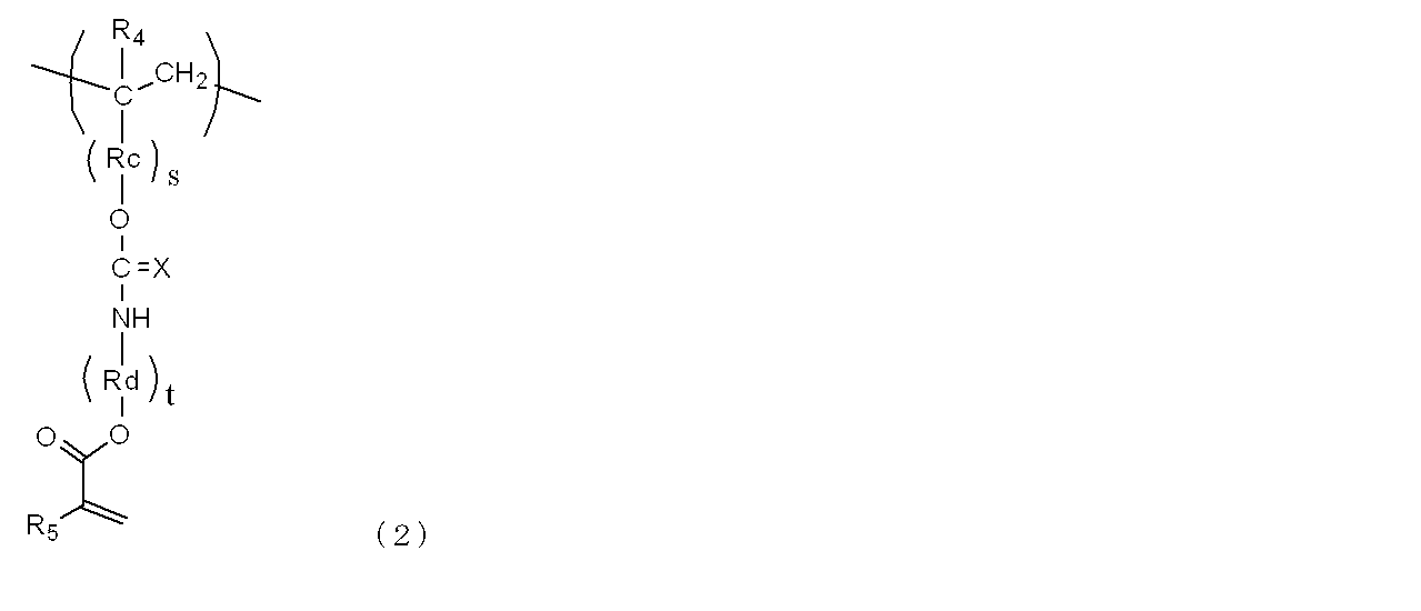
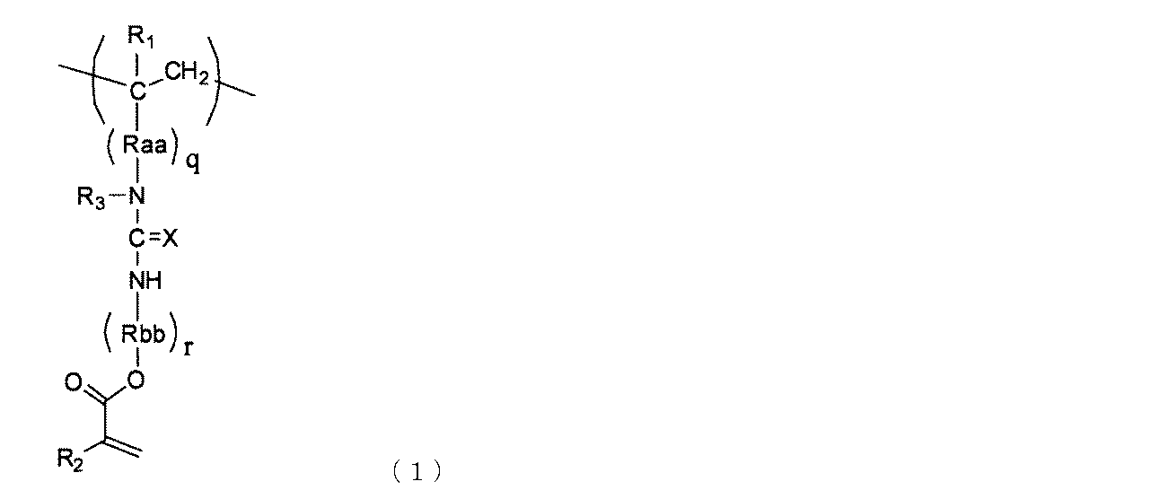
- the polymer compound containing a repeating unit having a photosensitive group bonded through a urea bond or a urethane bond is represented by the repeating unit represented by the general formula (1) and the general formula (2).
- R 1 and R 2 are the same or different and each represents a hydrogen atom or a methyl group
- R 3 represents a monovalent organic group having 1 to 20 carbon atoms
- Raa and Rbb are the same or different
- it represents a divalent organic group having 1 to 20 carbon atoms
- a hydrogen atom in the divalent organic group may be substituted with a fluorine atom
- X represents an oxygen atom or a sulfur atom
- q represents
- R represents an integer of 0 to 20
- r represents an integer of 1 to 20.
- R 4 and R 5 are the same or different and represent a hydrogen atom or a methyl group
- Rc and Rd are the same or different and represent a divalent organic group having 1 to 20 carbon atoms.
- the hydrogen atom in the valent organic group may be substituted with a fluorine atom
- X represents an oxygen atom or a sulfur atom
- s represents an integer of 0 to 20
- t represents an integer of 1 to 20.
- Rc when there are a plurality of Rc, they may be the same or different.
- Rd When there are a plurality of Rd, they may be the same or different.
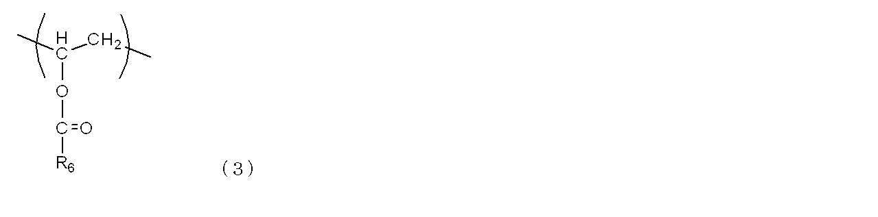
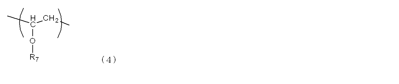
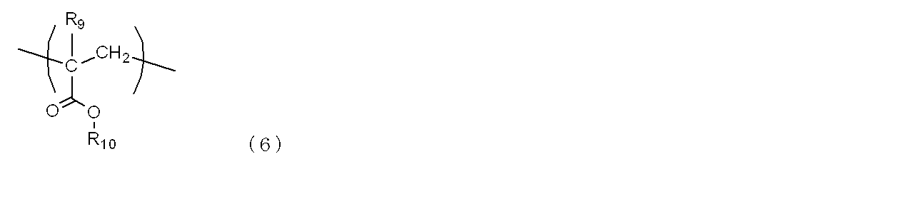
- the polymer compound further includes a repeating unit represented by the general formula (3), a repeating unit represented by the general formula (4), a repeating unit represented by the general formula (5), and It provides at least one repeating unit selected from the group consisting of repeating units represented by the general formula (6).
- R 6 represents a monovalent organic group having 1 to 20 carbon atoms.
- a hydrogen atom in the monovalent organic group may be substituted with a fluorine atom.
- R 7 represents a monovalent organic group having 1 to 20 carbon atoms.
- a hydrogen atom in the monovalent organic group may be substituted with a fluorine atom.
- R 8 represents a monovalent organic group or cyano group having 1 to 20 carbon atoms.
- a hydrogen atom in the monovalent organic group may be substituted with a fluorine atom.
- R 9 represents a hydrogen atom or a methyl group
- R 10 represents a monovalent organic group having 1 to 20 carbon atoms.
- the hydrogen atom in the divalent organic group is substituted with a fluorine atom. May be.
- the present invention provides an organic thin film transistor characterized by using the resin composition for an organic thin film transistor insulating layer as an overcoat layer.
- the present invention provides an organic thin film transistor characterized in that the resin composition for an organic thin film transistor insulating layer is used for a gate insulating layer.
- the present invention provides a display member comprising the resin composition for an organic thin film transistor insulating layer.
- the present invention provides a display comprising the display member.
- the resin composition for an insulating layer of the present invention can form a crosslinked structure and is excellent in electrical characteristics.
- it is photosensitive and does not need to be heated at a high temperature for a long time when the crosslinked structure is formed, so that the transistor characteristics are not adversely affected.
- the insulating layer to be formed has excellent surface adhesion, it is possible to easily form a laminated structure of organic layers including the insulating layer.
- the “polymer compound” refers to a compound having a structure in which a plurality of the same structural units are repeated in the molecule, and includes a so-called dimer.
- the “low molecular compound” means a compound that does not have the same structural unit repeatedly in the molecule.
- the resin composition for an organic thin film transistor insulating layer of the present invention comprises (A) a polymer compound containing a repeating unit having a photosensitive group bonded via a urea bond or a urethane bond, (B) a curing agent, and (C ) It is characterized by containing an organic solvent.
- Polymer compound (A) The polymer compound used in the present invention contains a repeating unit having a photosensitive group bonded through a urea bond or a urethane bond.
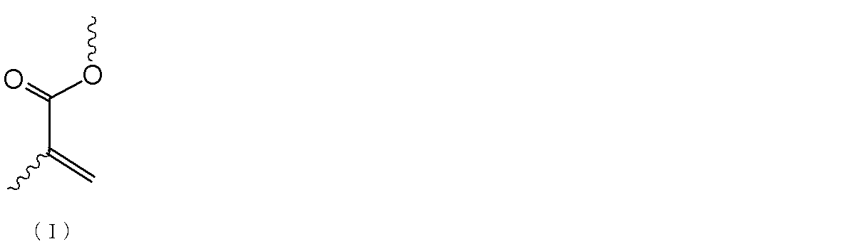
- the photosensitive group refers to a group that can be chemically changed by irradiating light or radiation.
- the polymer compound is preferably a polymer compound containing at least one repeating unit selected from the group consisting of the repeating unit represented by the general formula (1) and the repeating unit represented by the general formula (2). .
- any one of the repeating units represented by the general formulas (1) to (6) preferably contains a fluorine atom. This is because the presence of fluorine atoms in the resin structure improves electrical characteristics such as insulation of the formed layer.
- the fluorine atom is preferably present as a substituent of the organic group in the side chain portion of the repeating unit. This is because the surface adhesion of the layer to be formed is less likely to be lower than when the fluorine atom is substituted for the main chain portion.
- the amount of fluorine introduced into the polymer compound (A) is preferably 60% by mass or less, more preferably 5 to 50% by mass, and further preferably 5 to 40% by mass with respect to the mass of the polymer compound. .
- the amount of fluorine exceeds 60% by mass, the surface adhesion of the formed layer tends to be lowered.
- R 1 , R 2 , R 4 and R 5 are the same or different and each represents a hydrogen atom or a methyl group
- R 3 is a hydrogen atom or a carbon number of 1
- R 1 and R 4 is hydrogen atom
- R 2 and R 5 is a methyl group
- R 3 is hydrogen atom.
- Raa, Rbb, Rc and Rd are the same or different and represent a divalent organic group having 1 to 20 carbon atoms.
- a hydrogen atom in the divalent organic group may be substituted with a fluorine atom.
- X represents an oxygen atom or a sulfur atom
- q and s represent an integer of 0 to 20
- r and t represent an integer of 1 to 20.
- Raa they may be the same or different.
- Rbbs they may be the same or different.
- Rc they may be the same or different.
- Rd they may be the same or different.
- X is an oxygen atom and q, r, s, and t are 1.
- the divalent organic group having 1 to 20 carbon atoms may be linear, branched or cyclic, for example, a linear aliphatic hydrocarbon group having 1 to 20 carbon atoms, or 3 to 20 carbon atoms.
- Aromatic hydrocarbon having 6 to 20 carbon atoms which may be substituted with a linear hydrocarbon group having 6 to 6, a branched hydrocarbon group having 3 to 6 carbon atoms, a cyclic hydrocarbon group having 3 to 6 carbon atoms, an alkyl group, or the like A group hydrocarbon group is preferred.
- aliphatic hydrocarbon group examples include methylene group, ethylene group, propylene group, butylene group, pentylene group, hexylene group, isopropylene group, isobutylene group, dimethylpropylene group, cyclopropylene group, cyclobutylene group, cyclohexane.
- a pentylene group, a cyclohexylene group, etc. are mentioned.
- divalent aromatic hydrocarbon group having 6 to 20 carbon atoms include phenylene group, naphthylene group, anthrylene group, dimethylphenylene group, trimethylphenylene group, ethylenephenylene group, diethylenephenylene group, triethylenephenylene group, Examples thereof include a propylene phenylene group, a butylene phenylene group, a methyl naphthylene group, a dimethyl naphthylene group, a trimethyl naphthylene group, a vinyl naphthylene group, an ethenylene naphthylene group, a methyl anthrylene group, and an ethyl anthrylene group.
- Raa and Rc are phenylene groups.
- Rbb and Rd are ethylene groups.
- the monovalent organic group having 1 to 20 carbon atoms may be linear, branched or cyclic, and may be saturated or unsaturated.
- Examples of the monovalent organic group having 1 to 20 carbon atoms include a linear hydrocarbon group having 1 to 20 carbon atoms, a branched hydrocarbon group having 3 to 20 carbon atoms, and a cyclic hydrocarbon having 3 to 20 carbon atoms.
- the hydrogen atoms contained in these groups are substituted with fluorine atoms. May be.
- a hydrogen atom in the group may be substituted with an alkyl group, a fluoroalkyl group, a halogen atom or the like.
- the monovalent organic group having 1 to 20 carbon atoms include methyl group, ethyl group, propyl group, butyl group, pentyl group, hexyl group, isopropyl group, isobutyl group, tertiary butyl group, cyclopropyl group, Cyclobutyl group, cyclopentyl group, cyclohexyl group, cyclopentynyl group, cyclohexynyl group, trifluoromethyl group, trifluoroethyl group, phenyl group, naphthyl group, anthryl group, tolyl group, xylyl group, dimethylphenyl group, trimethylphenyl group , Ethylphenyl group, diethylphenyl group, triethylphenyl group, propylphenyl group, butylphenyl group, methylnaphthyl group, dimethylnaphthyl group,
- the polymer compound used in the present invention further includes a repeating unit represented by the general formula (3), a repeating unit represented by the general formula (4), a repeating unit represented by the general formula (5), and the general formula.
- R 6 , R 7 and R 10 are the same or different and represent a monovalent organic group having 1 to 20 carbon atoms.
- a hydrogen atom in the monovalent organic group may be substituted with a fluorine atom.
- R 8 represents a monovalent organic group having 1 to 20 carbon atoms or a cyano group.
- a hydrogen atom in the monovalent organic group may be substituted with a fluorine atom.
- R 9 represents a hydrogen atom or a methyl group. Specific examples of the monovalent organic group having 1 to 20 carbon atoms are the same as those already described.
- R 6 or R 8 is a group selected from the group consisting of a phenyl group, an o-fluoroalkylphenyl group and a p-fluoroalkylphenyl group.
- any of R 6 and R 8 is a group selected from the group consisting of a phenyl group and an o-fluoroalkylphenyl group.
- a preferred specific example of the o-fluoroalkylphenyl group is an o-trifluoromethylphenyl group.
- a preferred specific example of the p-fluoroalkylphenyl group is a p-trifluoromethylphenyl group.
- the polymer compound used in the present invention comprises a polymerizable monomer, which contains a group containing active hydrogen and serves as a raw material for the repeating unit represented by the general formula (1) and the general formula (2), as a photopolymerization initiator or heat. After polymerization using a polymerization initiator, it can be produced by a method of reacting with an acrylate compound containing an isocyanato group or isothiocyanato group in the molecule or a methacrylate compound containing an isocyanato group or isothiocyanato group in the molecule.
- the polymer compound used in the present invention is a repeating unit represented by the general formula (3), a repeating unit represented by the general formula (4), a repeating unit represented by the general formula (5), and the general formula (6).
- a repeating unit represented by the formula (1) and the raw material of the repeating unit represented by the general formula (2) containing a group containing active hydrogen
- a polymerizable monomer that is a raw material of the repeating unit represented by the general formulas (3) to (6) are copolymerized using a photopolymerization initiator or a thermal polymerization initiator.
- Examples of the polymerizable monomer that contains a group containing active hydrogen and serves as a raw material for the repeating unit represented by the general formula (1) and the general formula (2) include 4-aminostyrene, 4-allylaniline, 4-aminophenyl vinyl ether 4- (N-phenylamino) phenyl allyl ether, 4- (N-methylamino) phenyl allyl ether, 4-aminophenyl allyl ether, allylamine, 2-aminoethyl acrylate, 4-hydroxystyrene, 4-hydroxyallylbenzene 4-hydroxyphenyl vinyl ether, 4-hydroxyphenyl allyl ether, 4-hydroxybutyl vinyl ether, vinyl alcohol, 2-hydroxyethyl acrylate, 2-hydroxypropyl acrylate, 3-hydroxypropyl acrylate, acrylic acid -Hydroxybutyl, 4-hydroxyphenyl acrylate, 2-hydroxyphenylethyl acrylate 2-aminoethyl methacryl
- Examples of the acrylate compound containing an isocyanato group or an isothiocyanato group in the molecule include 2-acryloyloxyethyl isocyanate and 2-acryloyloxyethyl isothiocyanate.
- Examples of the methacrylate compound containing an isocyanato group or an isothiocyanato group in the molecule include 2-methacryloyloxyethyl isocyanate, 2- (2′-methacryloyloxyethyl) oxyethyl isocyanate, 2-methacryloyloxyethyl isothiocyanate, 2- (2 '-Methacryloyloxyethyl) oxyethyl isothiocyanate and the like.
- Examples of the polymerizable monomer used as a raw material for the repeating unit represented by the general formula (3) include vinyl acetate, vinyl propionate, vinyl butyrate, vinyl benzoate, vinyl-2-methylbenzoate, vinyl-3-methylbenzoate, Examples thereof include vinyl-4-methylbenzoate, vinyl-2-trifluoromethylbenzoate, vinyl-3-trifluoromethylbenzoate, vinyl-4-trifluoromethylbenzoate and the like.
- Examples of the polymerizable monomer that is a raw material for the repeating unit represented by the general formula (4) include vinyl methyl ether, vinyl ethyl ether, vinyl propyl ether, vinyl butyl ether, vinyl phenyl ether, vinyl benzyl ether, vinyl-4-methylphenyl. Examples include ether and vinyl-4-trifluoromethylphenyl ether.
- Examples of the polymerizable monomer that is a raw material for the repeating unit represented by the general formula (5) include styrene, ⁇ -methylstyrene, 2,4-dimethyl- ⁇ -methylstyrene, o-methylstyrene, m-methylstyrene, p.
- Examples of the polymerizable monomer that is a raw material for the repeating unit represented by the general formula (6) include methyl acrylate, ethyl acrylate, acrylate-n-propyl, isopropyl acrylate, acrylate-n-butyl, and isobutyl acrylate.
- photopolymerization initiator examples include acetophenone, 2,2-dimethoxy-2-phenylacetophenone, 2,2-diethoxyacetophenone, 4-isopropyl-2-hydroxy-2-methylpropiophenone, 2-hydroxy-2 -Methylpropiophenone, 4,4'-bis (diethylamino) benzophenone, benzophenone, methyl (o-benzoyl) benzoate, 1-phenyl-1,2-propanedione-2- (o-ethoxycarbonyl) oxime, 1- Phenyl-1,2-propanedione-2- (o-benzoyl) oxime, benzoin, benzoin methyl ether, benzoin ethyl ether, benzoin isopropyl ether, benzoin isobutyl ether, benzoin octyl ether, benzyl, benzyl dimethyl ketone
- carbonyl compounds such as tar, benzyl,
- thermal polymerization initiator may be used as long as it is an initiator for radical polymerization.
- 2,2′-azobisisobutyronitrile, 2,2′-azobisisovaleronitrile, 2,2′- Azobis (2,4-dimethylvaleronitrile), 4,4'-azobis (4-cyanovaleric acid), 1,1'-azobis (cyclohexanecarbonitrile), 2,2'-azobis (2-methylpropane) Azo compounds such as 2,2′-azobis (2-methylpropionamidine) dihydrochloride, ketone peroxides such as methyl ethyl ketone peroxide, methyl isobutyl ketone peroxide, cyclohexanone peroxide, acetylacetone peroxide, isobutyl peroxide Benzoyl peroxide, 2,4-dichlorobenzoyl peroxide, o Diacyl peroxides such as methylbenzoyl peroxide, la
- the polymer compound used in the present invention has a weight average molecular weight of preferably 3,000 to 1,000,000, more preferably 5,000 to 500,000, and may be linear, branched or cyclic.
- the charged molar amount of the polymerizable monomer which is a raw material of the repeating unit represented by the general formula (1) and the general formula (2) including the group containing the active hydrogen used in the present invention is the sum of all monomers used for the polymerization. On the other hand, it is preferably 1 mol% or more and 95 mol% or less, more preferably 5 mol% or more and 80 mol% or less, and still more preferably 10 mol% or more and 70 mol% or less.
- polymer compound used in the present invention examples include poly ⁇ styrene-co-pentafluorostyrene-co- [4-[(2′-methacryloyloxyethyl) aminocarbonylamino] -styrene] ⁇ , poly ⁇ styrene- Co-pentafluorostyrene-co-acrylonitrile-co- [4-[(2'-methacryloyloxyethyl) aminocarbonylamino] -styrene] ⁇ , poly ⁇ vinylbenzoate-co-pentafluorostyrene-co- [4- [ (2′-methacryloyloxyethyl) aminocarbonylamino] -styrene] ⁇ , poly ⁇ vinylbenzoate-co-pentafluorostyrene-co-acrylonitrile-co- [4-[(2′-methacryloyloxyethyl) aminocarbonylamino
- Curing agent (B) examples of the curing agent (B) used in the present invention include organic azo compounds and organic peroxides.
- examples of the organic diazo compound include 2,2′-azobisisobutyronitrile, 2,2′-azobisisovaleronitrile, 2,2′-azobis (2,4-dimethylvaleronitrile), 4, 4′-azobis (4-cyanovaleric acid), 1,1′-azobis (cyclohexanecarbonitrile), 2,2′-azobis (2-methylpropane), 2,2′-azobis (2-methylpropionamidine) And azobisisobutyronitrile such as dihydrochloride.
- organic peroxide examples include ketone peroxides such as methyl ethyl ketone peroxide, methyl isobutyl ketone peroxide, cyclohexanone peroxide, and acetylacetone peroxide, isobutyl peroxide, benzoyl peroxide, and 2,4-dichlorobenzoyl peroxide.
- Diacyl peroxides such as o-methylbenzoyl peroxide, lauroyl peroxide, p-chlorobenzoyl peroxide, 2,4,4-trimethylpentyl-2-hydroperoxide, diisopropylbenzene peroxide, cumene hydroperoxide, Hydroperoxides such as t-butyl peroxide, dicumyl peroxide, t-butylcumyl peroxide, di-t-butyl peroxide, tris (t-butylperoxy) Dialkyl peroxides such as lyazine, peroxyketals such as 1,1-di-t-butylperoxycyclohexane, 2,2-di (t-butylperoxy) butane, t-butylperoxypivalate, t -Butylperoxy-2-ethylhexanoate, t-butylperoxyisobutyrate, di-t-buty
- the curing agent used in the present invention preferably has a 10-hour half-life temperature of 30 ° C. to 200 ° C., more preferably a 10-hour half-life temperature of 40 ° C. to 150 ° C., and even more preferably 10 hours.
- the half-life temperature is 40 ° C to 100 ° C.
- the 10-hour half-life temperature is lower than 30 ° C, the storage stability is poor and gelation may occur, and when it is higher than 200 ° C, the organic semiconductor compound may be adversely affected during curing.
- Organic solvent (C) The organic solvent used in the present invention includes (A) at least one repeating unit selected from the group consisting of the repeating unit represented by the general formula (1) and the repeating unit represented by the general formula (2). There is no particular limitation as long as it is a good solvent for the polymer compound and the (B) curing agent and is a poor solvent for the organic semiconductor compound.
- a good solvent for the polymer compound and the (B) curing agent There is a poor solvent for the organic semiconductor compound.
- butyl acetate, 2-heptanone, propylene Examples include glycol monomethyl ether acetate.
- the resin composition for an organic thin film transistor insulating layer of the present invention contains at least one repeating unit selected from the group consisting of the repeating unit represented by the general formula (1) and the repeating unit represented by the general formula (2).
- the weight of the organic solvent is preferably 50 to 1000 parts by weight.
- the polymer compound containing at least one type of repeating unit selected from the group consisting of the repeating unit represented by the general formula (1) and the repeating unit represented by the general formula (2) 100 parts by weight of the polymer compound containing at least one type of repeating unit selected from the group consisting of the repeating unit represented by the general formula (1) and the repeating unit represented by the general formula (2)
- the weight of the curing agent is preferably 0.1 to 10 parts by weight.
- a crosslinking agent, a leveling agent, a surfactant, and the like can be added to the resin composition for an organic thin film transistor insulating layer of the present invention as necessary.
- the crosslinking agent include a low molecular compound containing two or more unsaturated double bonds in the molecule, a crosslinking agent for acrylic resin, and the like.
- the low molecular weight compound containing two or more unsaturated double bonds in the molecule include divinylbenzene and trimethylolpropane trimethacrylate.
- the crosslinking agent for acrylic resin include dicumyl peroxide and 4,4-di-tertiary butyl peroxy-n-butyl valerate.
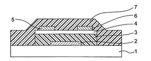
- FIG. 1 is a schematic cross-sectional view showing the structure of a bottom gate type organic thin film transistor which is an embodiment of the present invention.
- the organic thin film transistor includes a substrate 1, a gate electrode 2 formed on the substrate 1, a gate insulating layer 3 formed on the gate electrode 2, an organic semiconductor layer 4 formed on the gate insulating layer 3, A source electrode 5 and a drain electrode 6 formed on the organic semiconductor layer 4 with a channel portion interposed therebetween, and an overcoat 7 covering the entire element are provided.
- One embodiment of the method for producing the organic thin film transistor includes (i) a step of forming a gate electrode on a substrate, (ii) a step of forming a gate insulating layer on the gate electrode, and (iii) an organic semiconductor layer on the gate insulating layer. (Iv) forming a source electrode and a drain electrode on the organic semiconductor layer, and (v) forming an overcoat layer so as to cover the entire element. At least one of the gate insulating layer formed in step (ii) and the overcoat layer formed in step (v) is obtained by applying, drying and curing a resin solution containing the resin composition for an organic thin film transistor insulating layer of the present invention. Form.
- Examples of the material for the gate electrode formed in step (i) include chrome, gold, silver, and aluminum.
- the gate electrode can be formed by a known method such as an evaporation method, a sputtering method, a printing method, or an ink jet method.
- the resin solution containing the resin composition for an organic thin film transistor insulating layer of the present invention is used when forming the gate insulating layer in the step (ii), as the organic solvent contained in the resin solution, the resin composition to be used is dissolved.
- the organic solvent include 2-heptanone and propylene glycol monomethyl ether acetate.
- a leveling agent, a curing catalyst, and the like can be added to the resin solution as necessary.
- the gate insulating layer coating solution can be applied onto the gate electrode by known spin coating, die coater, screen printing, ink jet, or the like.
- a self-assembled monolayer may be formed on the gate insulating layer.
- the self-assembled monolayer can be formed, for example, by treating the gate insulating layer with a solution obtained by dissolving 1 to 10% by mass of an alkylchlorosilane compound or an alkylalkoxysilane compound in an organic solvent.
- the alkylchlorosilane compound include methyltrichlorosilane, ethyltrichlorosilane, butyltrichlorosilane, decyltrichlorosilane, octadecyltrichlorosilane, and the like.
- alkylalkoxysilane compound examples include methyltrimethoxysilane, ethyltrimethoxysilane, butyltrimethoxysilane, decyltrimethoxysilane, octadecyltrimethoxysilane and the like.
- the formation of the organic semiconductor layer in step (iii) is usually performed by applying and drying an organic semiconductor coating solution obtained by dissolving an organic semiconductor compound in an organic solvent.
- the organic solvent used in the organic semiconductor coating solution is not particularly limited as long as it dissolves the organic semiconductor compound, but preferably has a boiling point of 50 ° C. to 200 ° C. at normal pressure.
- Examples of the organic solvent include chloroform, toluene, anisole, 2-heptanone, propylene glycol monomethyl ether acetate and the like.
- the organic semiconductor coating solution can also be applied onto the gate insulating layer by a known spin coating, die coater, screen printing, ink jet or the like, similar to the gate insulating layer coating solution.
- Examples of the source electrode material and the drain electrode material formed in step (iv) include chrome, gold, silver, and aluminum.
- the source electrode and drain electrode can be formed in the same manner as the gate electrode.
- a known spin coat or die coat method is used as in the case of forming the gate insulating layer. It can be applied onto the organic semiconductor layer by a printer, screen printing, ink jet or the like.
- the curing temperature is preferably 50 ° C. to 250 ° C., more preferably 60 ° C. to 230 ° C., and still more preferably 80 ° C. to 200 ° C.
- the curing time can be appropriately selected according to the curing temperature.
- the curing temperature is lower than 50 ° C., curing may be insufficient, and when it is higher than 250 ° C., the polymer compound may be thermally decomposed.
- a known hot plate, oven, far-infrared baking furnace or the like can be used, and there is no particular limitation in the atmosphere or in an inert gas atmosphere, but preferably in an inert gas atmosphere.
- FIG. 2 is a schematic cross-sectional view showing the structure of a top gate type organic thin film transistor which is another embodiment of the present invention.
- the organic thin film transistor includes a substrate 1, a source electrode 5 and a drain electrode 6 formed on the substrate 1, an organic semiconductor layer 4 formed on these electrodes with a channel portion interposed therebetween, and an organic semiconductor layer 4 A gate insulating layer 3 covering the entire element formed on the gate insulating layer 3 and a gate electrode 2 formed on the surface of the gate insulating layer 3 are provided.
- One aspect of the method for producing the organic thin film transistor includes (a) a step of forming a source electrode and a drain electrode on a substrate, (b) a step of forming an organic semiconductor layer on the source electrode and the drain electrode, and (c) an organic semiconductor. Forming a gate insulating layer on the layer; and (d) forming a gate electrode on the gate insulating layer.
- the gate insulating layer formed in the step (d) is formed by applying, drying and curing a resin solution containing the resin composition for an organic thin film transistor insulating layer of the present invention.
- the insulating layer produced using the resin composition for an organic thin film transistor insulating layer of the present invention can be laminated with a flat film or the like, and can easily form a laminated structure. Moreover, an organic electroluminescent element can be suitably mounted on the insulating layer.
- the display member which has an organic thin-film transistor suitably can be produced using the organic thin-film transistor of the present invention.
- a display member having the organic thin film transistor a display including the display member can be suitably produced.
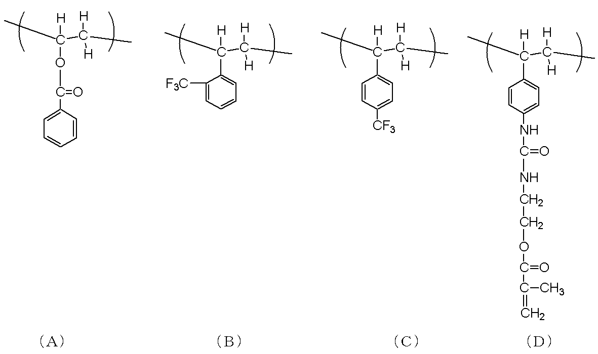
- Polymer compound 1 has a repeating unit represented by formula (A) to formula (D).
- Example 1> (Preparation of resin composition for organic thin film transistor insulating layer) A 2-heptanone solution of polymer compound 1 (3.00 g) and tertiary amyl peroxyisopropyl carbonate (AIC-75, manufactured by Kayaku Akzo) (0.036 g) are placed in a 10 ml sample bottle and dissolved with stirring to obtain a uniform coating solution. Prepared. The obtained coating solution was filtered using a membrane filter having a pore size of 0.2 ⁇ m to prepare a coating solution of polymer compound 1.
- AIC-75 tertiary amyl peroxyisopropyl carbonate
- % Solution organic semiconductor composition
- Vacuum deposition method using a metal mask on an n-type crystal silicon substrate which is a gate electrode with a thermal oxide film made of silicon dioxide (SiO 2 ) with a thickness of 300 nm
- a source electrode and a drain electrode having a laminated structure in the order of chromium and gold from the insulating layer side
- a bottom gate bottom contact transistor was manufactured by applying the film by spin coating and baking at 100 ° C. for 10 minutes to form an active layer having a thickness of about 60 nm.
- the field effect type having an overcoat layer having a thickness of 500 nm is baked at 200 ° C. for 1 minute on a hot plate in a nitrogen atmosphere. An organic thin film transistor was produced.
- the field-effect organic thin film transistor thus fabricated has the transistor characteristics of an on-voltage (Von voltage), ON under the condition that the gate voltage Vg is changed to 10 to ⁇ 60 V and the source-drain voltage Vsd is changed to 0 to ⁇ 60 V.
- / ON ratio and on-current density (Ion A / cm 2 ) at ⁇ 60 V were measured using a vacuum probe (BCT22MDC-5-HT-SCU; manufactured by Nagase Electronic Equipments Service Co. LTD). The results are shown in Table 2.
- a coating solution of polymer compound 1 is coated on a silicon substrate having aluminum deposited on the back surface, and baked at 200 ° C. for 1 minute in a nitrogen atmosphere to form an insulating layer (film thickness 507 nm).
- a metal mask is formed on the insulating layer.
- An evaluation electrode was prepared by vapor-depositing an aluminum electrode using The electrical characteristics of the obtained evaluation element were measured using a vacuum probe (BCT22MDC-5-HT-SCU; manufactured by Nagase Electronic Equipments Service Co. LTD). The results are shown in Table 1.
- a coating solution of the polymer compound 1 is coated on a silicon substrate, baked at 200 ° C. for 1 minute in a nitrogen atmosphere to form an insulating layer (film thickness 507 nm), and an aluminum electrode is formed on the insulating layer using a metal mask. Vapor deposited. When the Kapton tape was stuck on the aluminum electrode and the Kapton tape was peeled off, there was no peeling of the aluminum electrode.
- Example 1 (Production of field-effect organic thin-film transistors) A field effect organic thin film transistor was produced in the same manner as in Example 1 except that the coating solution of the polymer compound 1 was not applied, and the on-voltage (Von voltage), ON / OFF, which is the transistor characteristic of the field effect organic thin film transistor. The ratio and on-current density (Ion A / cm 2 ) at ⁇ 60V were measured. The results are shown in Table 2.
- ⁇ Evaluation Example 1> ⁇ Adhesiveness of fluororesin> Cytop (manufactured by Asahi Glass), which is a fluororesin, is applied on a silicon substrate and baked at 200 ° C. for 10 minutes in a nitrogen atmosphere to form an insulating layer (film thickness 1 ⁇ m). Aluminum is then formed on the insulating layer using a metal mask. Electrode was deposited. When the Kapton tape was stuck on the aluminum electrode and the Kapton tape was peeled off, the aluminum electrode was peeled off.
Landscapes
- Chemical & Material Sciences (AREA)
- Health & Medical Sciences (AREA)
- Chemical Kinetics & Catalysis (AREA)
- Medicinal Chemistry (AREA)
- Polymers & Plastics (AREA)
- Organic Chemistry (AREA)
- General Chemical & Material Sciences (AREA)
- Addition Polymer Or Copolymer, Post-Treatments, Or Chemical Modifications (AREA)
- Thin Film Transistor (AREA)
- Macromonomer-Based Addition Polymer (AREA)
Abstract
Description




なお、本明細書において、「高分子化合物」とは、分子中に同じ構造単位が複数繰り返された構造を含む化合物をいい、いわゆる2量体もこれに含まれる。一方、「低分子化合物」とは、分子中に同じ構造単位を繰り返し有していない化合物を意味する。
本発明に用いられる高分子化合物は、ウレア結合もしくはウレタン結合を介して結合した感光性基を有する繰り返し単位を含有する。ここで、感光性基とは光又は放射線を照射することにより化学変化しうる基をさし、具体的には、式
炭素数1~20の一価の有機基としては、例えば、炭素数1~20の直鎖状炭化水素基、炭素数3~20の分岐状炭化水素基、炭素数3~20の環状炭化水素基、炭素数6~20の芳香族炭化水素基が挙げられ、好ましくは、炭素数1~6の直鎖状炭化水素基、炭素数3~6の分岐状炭化水素基、炭素数3~6の環状炭化水素基、炭素数6~20の芳香族炭化水素基などが挙げられる。
炭素数1~20の直鎖状炭化水素基、炭素数3~20の分岐状炭化水素基、炭素数3~20の環状炭化水素基は、これらの基に含まれる水素原子がフッ素原子で置換されていてもよい。
炭素数6~20の芳香族炭化水素基は、基中の水素原子がアルキル基、フルオロアルキル基、ハロゲン原子などで置換されていてもよい。
炭素数1~20の一価の有機基としては、アルキル基が好ましい。
分子内にイソシアナト基もしくはイソチオシアナト基を含有するメタアクリレート化合物としては、2-メタクリロイルオキシエチルイソシアネート、2-(2‘-メタクリロイルオキシエチル)オキシエチルイソシアネート、2-メタクリロイルオキシエチルイソチオシアネート、2-(2‘-メタクリロイルオキシエチル)オキシエチルイソチオシアネート等が挙げられる。
本発明に用いられる(B)硬化剤としては、有機アゾ化合物ならびに有機過酸化物が挙げられる。
該有機ジアゾ化合物としては、例えば、2,2'-アゾビスイソブチロニトリル、2,2'-アゾビスイソバレロニトリル、2,2'-アゾビス(2,4-ジメチルバレロニトリル)、4,4’-アゾビス(4-シアノバレリックアシッド)、1、1’-アゾビス(シクロヘキサンカルボニトリル)、2,2’-アゾビス(2-メチルプロパン)、2,2’-アゾビス(2-メチルプロピオンアミジン)2塩酸塩等アゾビスイソブチロニトリル等が挙げられる。
該有機過酸化物としては、例えば、メチルエチルケトンパーオキシド、メチルイソブチルケトンパーオキシド、シクロヘキサノンパーオキシド、アセチルアセトンパーオキシド等のケトンパーオキシド類、イソブチルパーオキシド、ベンゾイルパーオキシド、2,4-ジクロロベンゾイルパーオキシド、o-メチルベンゾイルパーオキシド、ラウロイルパーオキシド、p-クロロベンゾイルパーオキシド等のジアシルパーオキシド類、2,4,4-トリメチルペンチル-2-ヒドロパーオキシド、ジイソプロピルベンゼンパーオキシド、クメンヒドロパーオキシド、t-ブチルパーオキシド等のヒドロパーオキシド類、ジクミルパーオキシド、t-ブチルクミルパーオキシド、ジ-t-ブチルパーオキシド、トリス(t-ブチルパーオキシ)トリアジン等のジアルキルパーオキシド類、1,1-ジ-t-ブチルパーオキシシクロヘキサン、2,2-ジ(t-ブチルパーオキシ)ブタン等のパーオキシケタール類、t-ブチルパーオキシピバレート、t-ブチルパーオキシ-2-エチルヘキサノエート、t-ブチルパーオキシイソブチレート、ジ-t-ブチルパーオキシヘキサヒドロテレフタレート、ジ-t-ブチルパーオキシアゼレート、t-ブチルパーオキシ-3,5,5-トリメチルヘキサノエート、t-ブチルパーオキシアセテート、t-ブチルパーオキシベンゾエート、ジ-t-ブチルパーオキシトリメチルアジペート等のアルキルパーエステル類、ジイソプロピルパーオキシジカーボネート、ジ-sec-ブチルパーオキシジカーボネート、t-アミルパーオキシイソプロピルカーボネート、t-ブチルパーオキシイソプロピルカーボネート等のパーオキシカーボネート類が挙げられる。
10時間半減期温度が30℃より低い場合、保存安定性が悪く、ゲル化することがあり、200℃より高い場合、硬化時に有機半導体化合物に悪影響を及ぼすことがある。
本発明に用いられる有機溶剤としては、(A)前記一般式(1)で表される繰り返し単位及び一般式(2)で表される繰り返し単位からなる群より選ばれる少なくとも1種の繰り返し単位を含有する高分子化合物ならびに(B)硬化剤に対して良溶媒であり、且つ、有機半導体化合物に対して貧溶媒であるものであれば特に制限はなく、例えば、酢酸ブチル、2-ヘプタノン、プロピレングリコールモノメチルエーテルアセテート等が挙げられる。
架橋剤としては、分子内に不飽和二重結合を二つ以上含有する低分子化合物、アクリル樹脂用架橋剤等が挙げられる。
該分子内に不飽和二重結合を二つ以上含有する低分子化合物としては、例えば、ジビニルベンゼン、トリメチロールプロパントリメタクリレート等が挙げられる。
該アクリル樹脂用架橋剤としては、ジキュミルパーオキサイド、4,4-ジ-ターシャリーブチルパーオキシ-n-ブチルバレレート等が挙げられる。
図1は、本発明の一実施形態であるボトムゲート型有機薄膜トランジスタの構造を示す模式断面図である。この有機薄膜トランジスタには、基板1と、基板1上に形成されたゲート電極2と、ゲート電極2上に形成されたゲート絶縁層3と、ゲート絶縁層3上に形成された有機半導体層4と、有機半導体層4上にチャネル部を挟んで形成されたソース電極5及びドレイン電極6と、素子全体を覆うオーバーコート7とが、備えられている。
該樹脂溶液には、必要に応じてレベリング剤、硬化触媒等を添加することが出来る。該ゲート絶縁層塗布溶液は公知のスピンコート、ダイコーター、スクリーン印刷、インクジェット等によりゲート電極上に塗布することが出来る。
該自己組織化単分子膜層は、例えば、有機溶媒中にアルキルクロロシラン化合物もしくはアルキルアルコキシシラン化合物を1~10質量%溶解した溶液でゲート絶縁層を処理することにより形成することが出来る。
該アルキルクロロシラン化合物としては、例えば、メチルトリクロロシラン、エチルトリクロロシラン、ブチルトリクロロシラン、デシルトリクロロシラン、オクタデシルトリクロロシラン等を例示できる。
該アルキルアルコキシシラン化合物としては、メチルトリメトキシシラン、エチルトリメトキシシラン、ブチルトリメトキシシラン、デシルトリメトキシシラン、オクタデシルトリメトキシシラン等を例示できる。
硬化方法は、公知のホットプレート、オーブン、遠赤外線ベーク炉等を用いることができ、大気中もしくは不活性ガス雰囲気中特に制限はないが、好ましくは、不活性ガス雰囲気中である。
ビニルベンゾエート(アルドリッチ製)8.47g、2-トリフルオロメチルスチレン(アルドリッチ製)6.16g、4-トリフルオロメチルスチレン(アルドリッチ製)6.16g、4-アミノスチレン(アルドリッチ製)1.70g、2,2’-アゾビス(イソブチロニトリル)0.22g、2-ヘプタノン(和光純薬製)52.93gを、125ml耐圧容器(エース製)に入れ、窒素をバブリングした後、密栓し、60℃のオイルバス中で48時間重合させて、粘稠な溶液を得た。
得られた粘調な溶液に2-メタクリロイルオキシエチルイソシアネート(昭和電工製、カレンズMOI)2.21gを加え、室温で24時間反応させ高分子化合物1の2-ヘプタノン溶液を得た。
(有機薄膜トランジスタ絶縁層用樹脂組成物の調製)
高分子化合物1の2-ヘプタノン溶液 3.00g、ターシャリーアミルパーオキシイソプロピルカーボネート(AIC-75、化薬アクゾ製)0.036gを10mlのサンプル瓶に入れ、攪拌溶解して均一な塗布溶液を調製した。
得られた塗布溶液を孔径0.2μmのメンブレンフィルターを用いてろ過し、高分子化合物1の塗布溶液を調製した。
F8T2(9,9-ジオクチルフルオレン:ビチオフェン=50:50(モル比)の共重合体;ポリスチレン換算の重量平均分子量=69,000)を溶媒であるクロロホルムに溶解して、濃度が0.5質量%である溶液(有機半導体組成物)を作製し、これをメンブランフィルターでろ過して有機半導体塗布液を調製した。
二酸化ケイ素(SiO2)からなる熱酸化膜が300nmの厚さで付いたゲート電極であるn型クリスタルシリコン基板(アドバンテック社製、比抵抗<0.1Ω)上にメタルマスクを用いた真空蒸着法により、チャネル長20μm、チャネル幅2mmのソース電極及びドレイン電極(絶縁層側から、クロム、金の順番で積層構造を有する)を形成し、次いで、電極を形成した基板上に有機半導体塗布溶液をスピンコート法により塗布し、100℃で10分間焼成を行い約60nmの厚さを有する活性層を形成し、ボトムゲートボトムコンタクト型トランジスタを作製した。
次に、得られたトランジスタ上に高分子化合物1の塗布溶液をスピンコートした後、窒素雰囲気中ホットプレート上で200℃で1分間焼成し、500nmの厚さのオーバーコート層を有する電界効果型有機薄膜トランジスタを作製した。
こうして作製した電界効果型有機薄膜トランジスタについて、ゲート電圧Vgを10~-60V、ソース・ドレイン間電圧Vsdを0~-60Vに変化させた条件で、そのトランジスタ特性であるオン電圧(Von電圧)、ON/OFF比及び-60Vにおけるオン電流密度(Ion A/cm2)を真空プロ-バ(BCT22MDC-5-HT-SCU;Nagase Electronic Equipments Service Co. LTD製)を用いて測定した。結果を表2に示す。
高分子化合物1の塗布溶液を裏面にアルミニウムを蒸着したシリコン基板上に塗布し、窒素雰囲気中で200℃で1分間焼成して絶縁層(膜厚507nm)を形成し、絶縁層上にメタルマスクを用いてアルミニウム電極を蒸着して評価素子を作成した。得られた評価素子の電気特性を真空プロ-バ(BCT22MDC-5-HT-SCU;Nagase Electronic Equipments Service Co. LTD製)を用いて測定した。結果を表1に示す。

高分子化合物1の塗布溶液をシリコン基板上に塗布し、窒素雰囲気中で200℃で1分間焼成して絶縁層(膜厚507nm)を形成し、絶縁層上にメタルマスクを用いてアルミニウム電極を蒸着した。アルミニウム電極上にカプトンテープを貼付し、カプトンテープを剥がしたところ、アルミニウム電極の剥れは無かった。
(電界効果型有機薄膜トランジスタの作製)
高分子化合物1の塗布溶液を塗布しない以外は、実施例1と同様にして電界効果型有機薄膜トランジスタを作製し、該電界効果型有機薄膜トランジスタのトランジスタ特性であるオン電圧(Von電圧)、ON/OFF比及び-60Vにおけるオン電流密度(Ion A/cm2)を測定した。結果を表2に示す。
<フッ素樹脂の密着性>
フッ素樹脂であるCytop(旭硝子製)をシリコン基板上に塗布し、窒素雰囲気中で200℃で10分間焼成して絶縁層(膜厚1μm)を形成し、絶縁層上にメタルマスクを用いてアルミニウム電極を蒸着した。アルミニウム電極上にカプトンテープを貼付し、カプトンテープを剥がしたところ、アルミニウム電極が剥れた。

2…ゲート電極、
3…ゲート絶縁層、
4…有機半導体層、
5…ソース電極、
6…ドレイン電極。
Claims (7)
- (A)ウレア結合もしくはウレタン結合を介して結合した感光性基を有する繰り返し単位を含有する高分子化合物と、(B)硬化剤と、(C)有機溶剤とを含有することを特徴とする有機薄膜トランジスタ絶縁層用樹脂組成物。
- ウレア結合もしくはウレタン結合を介して結合した感光性基を有する繰り返し単位を含有する高分子化合物が、一般式(1)で表される繰り返し単位及び一般式(2)で表される繰り返し単位からなる群より選ばれる少なくとも1種の繰り返し単位を含有する高分子化合物であることを特徴とする請求項1に記載の有機薄膜トランジスタ絶縁層用樹脂組成物。

- 高分子化合物が、さらに、一般式(3)で表される繰り返し単位、一般式(4)で表される繰り返し単位、一般式(5)で表される繰り返し単位及び一般式(6)で表される繰り返し単位からなる群より選ばれる少なくとも1種の繰り返し単位を含有することを特徴とする請求項1又は2に記載の有機薄膜トランジスタ絶縁層用樹脂組成物。

- 請求項1~3のいずれかに記載の有機薄膜トランジスタ絶縁層用樹脂組成物をオーバーコート層に用いることを特徴とした有機薄膜トランジスタ。
- 請求項1~3のいずれかに記載の有機薄膜トランジスタ絶縁層用樹脂組成物をゲート絶縁層に用いることを特徴とした有機薄膜トランジスタ。
- 請求項1~3のいずれかに記載の有機薄膜トランジスタ絶縁層用樹脂組成物を含むディスプレイ用部材。
- 請求項6に記載のディスプレイ用部材からなるディスプレイ。
Priority Applications (4)
| Application Number | Priority Date | Filing Date | Title |
|---|---|---|---|
| GB1113979A GB2480184A (en) | 2009-01-14 | 2010-01-07 | Resin compositions for insulating layer |
| CN2010800044936A CN102282186A (zh) | 2009-01-14 | 2010-01-07 | 绝缘层用树脂组合物 |
| DE112010000720T DE112010000720T5 (de) | 2009-01-14 | 2010-01-07 | Harzzusammensetzung für lsolierschicht |
| US13/144,237 US20120053287A1 (en) | 2009-01-14 | 2010-01-07 | Resin composition for insulating layer |
Applications Claiming Priority (2)
| Application Number | Priority Date | Filing Date | Title |
|---|---|---|---|
| JP2009005812A JP2010163521A (ja) | 2009-01-14 | 2009-01-14 | 絶縁層用樹脂組成物 |
| JP2009-005812 | 2009-01-14 |
Publications (1)
| Publication Number | Publication Date |
|---|---|
| WO2010082525A1 true WO2010082525A1 (ja) | 2010-07-22 |
Family
ID=42339778
Family Applications (1)
| Application Number | Title | Priority Date | Filing Date |
|---|---|---|---|
| PCT/JP2010/050082 Ceased WO2010082525A1 (ja) | 2009-01-14 | 2010-01-07 | 絶縁層用樹脂組成物 |
Country Status (8)
| Country | Link |
|---|---|
| US (1) | US20120053287A1 (ja) |
| JP (1) | JP2010163521A (ja) |
| KR (1) | KR20110119700A (ja) |
| CN (1) | CN102282186A (ja) |
| DE (1) | DE112010000720T5 (ja) |
| GB (1) | GB2480184A (ja) |
| TW (1) | TW201035123A (ja) |
| WO (1) | WO2010082525A1 (ja) |
Cited By (2)
| Publication number | Priority date | Publication date | Assignee | Title |
|---|---|---|---|---|
| JP2012072369A (ja) * | 2010-08-31 | 2012-04-12 | Fujifilm Corp | 重合性組成物、それを用いた平版印刷版原版、防汚性部材、及び、防曇性部材 |
| JP2012117058A (ja) * | 2010-11-10 | 2012-06-21 | Sumitomo Chemical Co Ltd | 有機素子材料 |
Families Citing this family (3)
| Publication number | Priority date | Publication date | Assignee | Title |
|---|---|---|---|---|
| WO2012074047A1 (ja) * | 2010-12-01 | 2012-06-07 | 日産化学工業株式会社 | 重合性含フッ素高分岐ポリマー及びそれを含む硬化性組成物 |
| CN104583257B (zh) * | 2012-08-31 | 2016-12-28 | 旭硝子株式会社 | 固化性组合物和固化膜的制造方法 |
| JP6118287B2 (ja) * | 2014-03-26 | 2017-04-19 | 富士フイルム株式会社 | 半導体素子及び半導体素子の絶縁層形成用組成物 |
Citations (4)
| Publication number | Priority date | Publication date | Assignee | Title |
|---|---|---|---|---|
| JP2005513788A (ja) * | 2001-12-19 | 2005-05-12 | アベシア・リミテッド | 有機誘電体を有する有機電界効果トランジスタ |
| JP2007305950A (ja) * | 2006-04-12 | 2007-11-22 | Toppan Printing Co Ltd | 絶縁塗料、これから形成された有機絶縁膜、その形成方法および有機トランジスタ |
| JP2009088316A (ja) * | 2007-10-01 | 2009-04-23 | Sumitomo Chemical Co Ltd | 有機トランジスタ絶縁膜用組成物 |
| WO2010024238A1 (ja) * | 2008-08-28 | 2010-03-04 | 住友化学株式会社 | 樹脂組成物、ゲート絶縁層及び有機薄膜トランジスタ |
Family Cites Families (1)
| Publication number | Priority date | Publication date | Assignee | Title |
|---|---|---|---|---|
| EP1170315A4 (en) * | 1999-03-19 | 2002-09-11 | Nippon Kayaku Kk | URETHANOLIGOMER, RESIN COMPOSITIONS AND HARDENED ITEMS |
-
2009
- 2009-01-14 JP JP2009005812A patent/JP2010163521A/ja not_active Withdrawn
-
2010
- 2010-01-07 CN CN2010800044936A patent/CN102282186A/zh active Pending
- 2010-01-07 US US13/144,237 patent/US20120053287A1/en not_active Abandoned
- 2010-01-07 GB GB1113979A patent/GB2480184A/en not_active Withdrawn
- 2010-01-07 WO PCT/JP2010/050082 patent/WO2010082525A1/ja not_active Ceased
- 2010-01-07 DE DE112010000720T patent/DE112010000720T5/de not_active Withdrawn
- 2010-01-07 KR KR1020117018793A patent/KR20110119700A/ko not_active Withdrawn
- 2010-01-11 TW TW099100498A patent/TW201035123A/zh unknown
Patent Citations (4)
| Publication number | Priority date | Publication date | Assignee | Title |
|---|---|---|---|---|
| JP2005513788A (ja) * | 2001-12-19 | 2005-05-12 | アベシア・リミテッド | 有機誘電体を有する有機電界効果トランジスタ |
| JP2007305950A (ja) * | 2006-04-12 | 2007-11-22 | Toppan Printing Co Ltd | 絶縁塗料、これから形成された有機絶縁膜、その形成方法および有機トランジスタ |
| JP2009088316A (ja) * | 2007-10-01 | 2009-04-23 | Sumitomo Chemical Co Ltd | 有機トランジスタ絶縁膜用組成物 |
| WO2010024238A1 (ja) * | 2008-08-28 | 2010-03-04 | 住友化学株式会社 | 樹脂組成物、ゲート絶縁層及び有機薄膜トランジスタ |
Cited By (2)
| Publication number | Priority date | Publication date | Assignee | Title |
|---|---|---|---|---|
| JP2012072369A (ja) * | 2010-08-31 | 2012-04-12 | Fujifilm Corp | 重合性組成物、それを用いた平版印刷版原版、防汚性部材、及び、防曇性部材 |
| JP2012117058A (ja) * | 2010-11-10 | 2012-06-21 | Sumitomo Chemical Co Ltd | 有機素子材料 |
Also Published As
| Publication number | Publication date |
|---|---|
| US20120053287A1 (en) | 2012-03-01 |
| KR20110119700A (ko) | 2011-11-02 |
| GB2480184A (en) | 2011-11-09 |
| DE112010000720T5 (de) | 2012-08-09 |
| TW201035123A (en) | 2010-10-01 |
| CN102282186A (zh) | 2011-12-14 |
| JP2010163521A (ja) | 2010-07-29 |
| GB201113979D0 (en) | 2011-09-28 |
Similar Documents
| Publication | Publication Date | Title |
|---|---|---|
| JP5479817B2 (ja) | 有機薄膜トランジスタゲート絶縁層用樹脂組成物、ゲート絶縁層及び有機薄膜トランジスタ | |
| US9035292B2 (en) | Organic thin-film transistor insulating layer material | |
| JP5695467B2 (ja) | 有機薄膜トランジスタ絶縁層用樹脂組成物、オーバーコート絶縁層及び有機薄膜トランジスタ | |
| US20120053287A1 (en) | Resin composition for insulating layer | |
| EP2797110B1 (en) | Insulation-layer material for electronic device, and electronic device | |
| JP5890633B2 (ja) | 有機薄膜トランジスタ絶縁層用組成物及び有機薄膜トランジスタ | |
| JP2011228678A (ja) | フッ素系有機化合物溶媒を含む有機薄膜トランジスタ絶縁層用組成物 | |
| EP2479791A1 (en) | Photo-crosslinkable material for organic thin film transistor insulating layer | |
| JP2016033945A (ja) | 組成物およびそれを用いた有機薄膜トランジスタ | |
| JP5980522B2 (ja) | 有機薄膜トランジスタ絶縁層材料 | |
| JP6056443B2 (ja) | 絶縁層材料及び該絶縁層材料を用いて形成した有機薄膜トランジスタ | |
| WO2012002436A1 (ja) | 有機薄膜トランジスタ絶縁層材料及び有機薄膜トランジスタ | |
| JP5938192B2 (ja) | 有機素子材料 | |
| JP2014175639A (ja) | 有機素子材料 | |
| JP2010037462A (ja) | ゲート絶縁層用樹脂組成物 | |
| JP2013258301A (ja) | 有機薄膜トランジスタ絶縁層材料 |
Legal Events
| Date | Code | Title | Description |
|---|---|---|---|
| WWE | Wipo information: entry into national phase |
Ref document number: 201080004493.6 Country of ref document: CN |
|
| 121 | Ep: the epo has been informed by wipo that ep was designated in this application |
Ref document number: 10731194 Country of ref document: EP Kind code of ref document: A1 |
|
| WWE | Wipo information: entry into national phase |
Ref document number: 1120100007209 Country of ref document: DE Ref document number: 112010000720 Country of ref document: DE |
|
| ENP | Entry into the national phase |
Ref document number: 1113979 Country of ref document: GB Kind code of ref document: A Free format text: PCT FILING DATE = 20100107 Ref document number: 20117018793 Country of ref document: KR Kind code of ref document: A |
|
| WWE | Wipo information: entry into national phase |
Ref document number: 1113979.7 Country of ref document: GB |
|
| WWE | Wipo information: entry into national phase |
Ref document number: 13144237 Country of ref document: US |
|
| 122 | Ep: pct application non-entry in european phase |
Ref document number: 10731194 Country of ref document: EP Kind code of ref document: A1 |