WO2010082435A1 - 表示パネル用の基板および表示パネル - Google Patents
表示パネル用の基板および表示パネル Download PDFInfo
- Publication number
- WO2010082435A1 WO2010082435A1 PCT/JP2009/071412 JP2009071412W WO2010082435A1 WO 2010082435 A1 WO2010082435 A1 WO 2010082435A1 JP 2009071412 W JP2009071412 W JP 2009071412W WO 2010082435 A1 WO2010082435 A1 WO 2010082435A1
- Authority
- WO
- WIPO (PCT)
- Prior art keywords
- seal pattern
- display panel
- region
- display
- substrate
- Prior art date
- Legal status (The legal status is an assumption and is not a legal conclusion. Google has not performed a legal analysis and makes no representation as to the accuracy of the status listed.)
- Ceased
Links
Images



Classifications
-
- G—PHYSICS
- G02—OPTICS
- G02F—OPTICAL DEVICES OR ARRANGEMENTS FOR THE CONTROL OF LIGHT BY MODIFICATION OF THE OPTICAL PROPERTIES OF THE MEDIA OF THE ELEMENTS INVOLVED THEREIN; NON-LINEAR OPTICS; FREQUENCY-CHANGING OF LIGHT; OPTICAL LOGIC ELEMENTS; OPTICAL ANALOGUE/DIGITAL CONVERTERS
- G02F1/00—Devices or arrangements for the control of the intensity, colour, phase, polarisation or direction of light arriving from an independent light source, e.g. switching, gating or modulating; Non-linear optics
- G02F1/01—Devices or arrangements for the control of the intensity, colour, phase, polarisation or direction of light arriving from an independent light source, e.g. switching, gating or modulating; Non-linear optics for the control of the intensity, phase, polarisation or colour
- G02F1/13—Devices or arrangements for the control of the intensity, colour, phase, polarisation or direction of light arriving from an independent light source, e.g. switching, gating or modulating; Non-linear optics for the control of the intensity, phase, polarisation or colour based on liquid crystals, e.g. single liquid crystal display cells
- G02F1/133—Constructional arrangements; Operation of liquid crystal cells; Circuit arrangements
- G02F1/136—Liquid crystal cells structurally associated with a semi-conducting layer or substrate, e.g. cells forming part of an integrated circuit
- G02F1/1362—Active matrix addressed cells
- G02F1/136286—Wiring, e.g. gate line, drain line
-
- G—PHYSICS
- G02—OPTICS
- G02F—OPTICAL DEVICES OR ARRANGEMENTS FOR THE CONTROL OF LIGHT BY MODIFICATION OF THE OPTICAL PROPERTIES OF THE MEDIA OF THE ELEMENTS INVOLVED THEREIN; NON-LINEAR OPTICS; FREQUENCY-CHANGING OF LIGHT; OPTICAL LOGIC ELEMENTS; OPTICAL ANALOGUE/DIGITAL CONVERTERS
- G02F1/00—Devices or arrangements for the control of the intensity, colour, phase, polarisation or direction of light arriving from an independent light source, e.g. switching, gating or modulating; Non-linear optics
- G02F1/01—Devices or arrangements for the control of the intensity, colour, phase, polarisation or direction of light arriving from an independent light source, e.g. switching, gating or modulating; Non-linear optics for the control of the intensity, phase, polarisation or colour
- G02F1/13—Devices or arrangements for the control of the intensity, colour, phase, polarisation or direction of light arriving from an independent light source, e.g. switching, gating or modulating; Non-linear optics for the control of the intensity, phase, polarisation or colour based on liquid crystals, e.g. single liquid crystal display cells
- G02F1/133—Constructional arrangements; Operation of liquid crystal cells; Circuit arrangements
- G02F1/136—Liquid crystal cells structurally associated with a semi-conducting layer or substrate, e.g. cells forming part of an integrated circuit
- G02F1/1362—Active matrix addressed cells
- G02F1/136286—Wiring, e.g. gate line, drain line
- G02F1/136295—Materials; Compositions; Manufacture processes
Definitions
- the present invention relates to a display panel substrate and a display panel, and more particularly to a display panel substrate suitable for a liquid crystal display panel and a display panel including the display panel substrate.
- a general liquid crystal display panel includes two substrates.
- an active matrix type liquid crystal display panel includes a TFT array substrate and a counter substrate (for example, a color filter). These substrates are arranged to face each other at a predetermined minute interval, and a liquid crystal is filled between these substrates.
- the filled liquid crystal is sealed with a sealing material formed so as to surround a region where picture elements are arranged. In other words, the liquid crystal is filled in a region surrounded by the sealing material.
- Various wiring patterns and thin film patterns such as a thin film transistor, a data line (also referred to as source wiring), a scanning line (also referred to as gate wiring), a semiconductor film, and a pixel electrode are formed on one surface of the TFT array substrate.
- An alignment film having a function of regulating the alignment of the liquid crystal is formed on the uppermost layer on the surface of the pixel electrode.
- a predetermined thin film pattern such as a black matrix, a colored layer, or a common electrode, a wiring pattern, or the like is formed on one surface of the color filter.
- An alignment film having a function of regulating liquid crystal alignment is formed in a predetermined region on the surface of the common electrode.
- a sealing material is applied to one of the TFT array substrate and the color filter so as to surround the region where the alignment film is formed, and the two substrates are bonded together. That is, when the TFT array substrate and the counter substrate (color filter) are bonded together, the sealing material is formed so as to surround the region where the alignment film is formed.
- a method for forming an alignment film using a rotary press is to apply an alignment material (solution that becomes a material for the alignment film) to a printing roller (printing plate), and apply the applied alignment material to a predetermined surface of a substrate for a display panel. It is to transfer to the area. According to such a method, there is an advantage that the alignment material can be accurately transferred (applied) to a predetermined region on the surface of the display panel substrate. On the other hand, there is a problem that a dedicated printing roller is required for each type of display panel substrate (especially for each screen size).
- the ink jet type printing machine is provided with a dropping nozzle, and this dropping nozzle drops the alignment material at a predetermined position on the surface of the substrate for the display panel.
- the dropped alignment material wets and spreads the surface of the display panel substrate. Then, the alignment materials that have spread out are connected to each other, whereby an alignment material layer is formed in a predetermined region on the surface of the display panel substrate.
- the sealing material is formed so as to surround the region where the alignment film is formed.
- the sealing material is not formed on the surface of the alignment film.
- the alignment material that has spread out reaches the position where the seal material is to be formed and the alignment film is formed at the position where the seal material is to be formed, the following problems may occur.
- the sealing material has a function of sealing the liquid crystal filled between the two substrates. For this reason, it is preferable that the sealing material is firmly adhered to the surface of the display panel substrate.
- the alignment film and the sealing material generally have low adhesion, when the alignment film is formed at a position where the sealing material is formed (in other words, the structure in which the sealing material is formed on the surface of the alignment film) The function of sealing the liquid crystal may be reduced.
- the alignment film is generally formed of polyimide. Since polyimide is a highly hygroscopic material, when the alignment film is exposed to the outside of the sealing material, there is a possibility that moisture may permeate into the region where the liquid crystal is sealed through the exposed alignment film.
- the problem to be solved by the present invention is to prevent the dropped alignment material from spreading in a direction where it should not be spread out when the alignment film is applied by an inkjet printer. It is possible to provide a display panel substrate and a display panel including the substrate, and in particular, a display panel substrate capable of preventing the dropped alignment material from spreading into the seal pattern region.
- a display panel provided with a substrate, or a substrate for a display panel capable of preventing a dropped alignment material from spreading out beyond a seal pattern region, and a display panel including the substrate.
- a substrate for a display panel capable of maintaining the degree of sealing of liquid crystal by a sealing material and the substrate To provide a display panel.
- the present invention provides a display area in which a plurality of pixel electrodes are arranged in a matrix, a seal pattern area formed so as to surround the display area, and an array in the display area.
- a wiring capable of transmitting a predetermined signal to a predetermined pixel, and an opening is formed in a portion of the wiring formed in a region between the display region and the seal pattern region It is the gist of what is done.
- the opening is preferably formed in a slit shape extending substantially parallel to the extending direction of the adjacent seal pattern region.
- the present invention provides a display area in which a plurality of picture element electrodes are arranged in a matrix, a seal pattern area formed so as to surround the display area, and a predetermined picture element arranged in the display area.
- a wiring capable of transmitting a signal, and an opening is formed in a portion of the wiring formed in the seal pattern region.
- the opening is preferably formed in a slit shape extending substantially parallel to the extending direction of the adjacent seal pattern region.
- the present invention provides a display area in which a plurality of picture element electrodes are arranged in a matrix, a seal pattern area formed so as to surround the display area, and a predetermined picture element arranged in the display area.
- a wiring that can transmit the signal of the wiring, and a portion of the wiring that is formed in a region between the display region and the seal pattern region has a portion that is formed in a folded shape.
- the portion formed in the zigzag shape includes a portion extending substantially parallel to the extending direction of the adjacent seal pattern region.
- the present invention provides a display area in which a plurality of picture element electrodes are arranged in a matrix, a seal pattern area formed so as to surround the display area, and a predetermined picture element arranged in the display area. And a wiring that can transmit the above signal, and a portion of the wiring that is formed in the seal pattern region includes a portion that is formed in a folded shape.
- the portion formed in the zigzag shape includes a portion extending substantially parallel to the extending direction of the adjacent seal pattern region.
- a data line can be suitably applied to the wiring. Further, a scanning line can be suitably applied to the wiring.
- the gist of the display panel according to the present invention is that the display panel includes the display panel substrate and a counter substrate.
- the dropped alignment material tends to flow along the wiring formed on the substrate for the display panel.
- the opening to be prevented prevents the alignment material from flowing. Therefore, the alignment material dropped on the region where the picture elements are arranged is prevented from flowing out to the seal pattern region through the wiring. For this reason, in the process of forming the sealing material, the sealing material is prevented from coming into contact with the alignment film (the sealing material is formed on the surface of the alignment film). With such a configuration, the adhesion between the display panel substrate and the sealing material can be maintained.
- the alignment material dropped on the region where the picture elements are arranged is prevented from flowing out of the seal pattern region through the wiring. This prevents the alignment film from being formed outside the seal pattern region. Therefore, since the alignment film is not exposed to the outside air, it is possible to prevent moisture in the outside air from entering the liquid crystal through the alignment film.
- the opening formed in the wiring extends in a direction substantially parallel to the extending direction of the adjacent seal pattern region, the flow of the dropped alignment material can be more effectively prevented. it can.
- the dropped alignment material tends to flow along the wiring formed on the display panel substrate.
- the zigzag folded portion formed in the block prevents the flow of the alignment material. Therefore, the same operational effects as described above can be achieved.
- the zigzag folded portion has a portion extending in a direction substantially parallel to the extending direction of the adjacent seal pattern region, the flow of the dropped orientation material can be more effectively prevented. it can.
- a substrate for a display panel according to each embodiment of the present invention is a TFT array substrate applied to an active matrix type liquid crystal display panel.
- FIG. 1 is an external perspective view schematically showing a schematic configuration of a display panel substrate 1a according to the first embodiment of the present invention and a display panel substrate 1b according to the second embodiment.
- the overall configuration of the display panel substrate 1a according to the first embodiment of the present invention and the display panel substrate 1b according to the second embodiment will be described.
- substrate 1b for display panels concerning 2nd embodiment is substantially the same, it demonstrates collectively.
- the display panel substrate 1a according to the first embodiment of the present invention and the display panel substrate 1b according to the second embodiment are provided with a display region 11 (also referred to as an active region).
- a panel frame area 12 is provided outside the display area 11 so as to surround the display area 11.
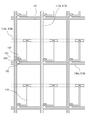
- FIG. 2 is a plan view schematically showing the configuration of picture elements and wirings provided in the display area 11.
- a plurality of picture elements are arranged in a matrix.
- Each picture element includes a picture element electrode 111 and a switching element 112 (specifically, for example, a thin film transistor (TFT)) that drives the picture element electrode 111.
- the drain electrode 115 of the switching element 112 and the picture element The electrode 111 is electrically connected by a drain wiring 119.
- a plurality of scanning lines 116a and 116b are provided in the display region 11 substantially in parallel with each other.
- auxiliary capacitance signal lines 118a and 118b are provided substantially parallel to the scanning lines 116a and 116b, and a plurality of data lines 117a and 117b (source wirings). are also substantially parallel to each other, and the scanning lines 116a and 116b and the auxiliary capacitance signal line 1 18a and 118b are provided so as to be substantially orthogonal.
- Each scanning line 116a, 116b is electrically connected to the gate electrode 113 of the switching element 112 of a predetermined plurality of picture elements.
- Each of the scanning lines 116a and 116b can transmit a gate signal (also referred to as a selection pulse) to the gate electrode 113 of the predetermined switching element 112.
- the auxiliary capacitance signal lines 118 a and 118 b form auxiliary capacitance (also referred to as storage capacitance) between the predetermined pixel electrodes 111.
- the data lines 117a and 117b are electrically connected to the source electrode 114 of the switching element 112 of a predetermined plurality of picture elements.
- the data lines 117a and 117b can transmit a data signal to the source electrode 114 of the predetermined switching element 112.
- a panel frame region 12 is provided around the display region 11 so as to surround the display region 11.
- the panel frame area 12 is provided with a terminal area 121 and a seal pattern area 123.
- the terminal area 121 is an area provided at or near the outer periphery of the panel frame area 12.
- wiring electrode terminals 122 are provided in the terminal region 121.
- the wiring electrode terminal 122 includes predetermined wiring (scanning lines 116a and 116b, auxiliary capacitance signal lines 118a and 118b, data lines 117a and 117b, etc.) extending from the display area 11, and a driver IC (also referred to as a driver LSI). It is a terminal for connecting to.
- an anisotropic conductive film (ACF: Anisotropic ⁇ Conductive TCP Film) is affixed to the terminal region 121 and a TCP (Tape ⁇ ⁇ Carrier Package) on which a driver IC (or driver LSI) is mounted is attached.
- the wiring electrode terminal 122 is fixed by a conductive film. According to such a configuration, a predetermined signal generated by a driver IC or the like mounted on the TCP is transmitted through the wiring electrode terminal 122 to a predetermined wiring (scanning lines 116a and 116b, auxiliary capacitance signal line provided in the display area 11). 118a, 118b and data lines 117a, 117b).
- a seal pattern area 123 is set.
- the seal pattern region 123 is a region where a seal pattern for sealing and holding the liquid crystal is formed (in other words, a region where a seal material is applied).
- the seal pattern is the first embodiment of the present invention when the display panel substrate 1a according to the first embodiment of the present invention or the display panel substrate 1b according to the second embodiment and the counter substrate are bonded together. Liquid crystal is sealed between the display panel substrate 1a according to the embodiment or the display panel substrate 1b according to the second embodiment of the present invention and the counter substrate (in other words, a liquid crystal layer is formed)
- the substrate is fixed to the display panel substrate 1a according to the first embodiment of the present invention or the display panel substrate 1b according to the second embodiment. As shown in FIG.
- the seal pattern region 123 is a region set so as to surround the display region 11 with a predetermined distance from the outer periphery of the display region 11.
- the seal pattern region 123 is a frame-like region having an open substantially quadrilateral shape, and each side of the quadrilateral has a predetermined width dimension.
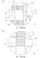
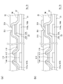
- FIG. 3 is a view showing a predetermined portion of the display panel substrate 1a according to the first embodiment of the present invention.
- 3A is an enlarged view of the portion B shown in FIG. 1
- FIG. 3B is an enlarged view of the portion C shown in FIG. That is, these drawings are plan views schematically showing the structure of the wiring formed in the panel frame region 12 of the display panel substrate 1a according to the first embodiment of the present invention.
- predetermined wirings are formed in the panel frame region 12. Specifically, as shown in FIG. 3A, scanning lines 116 a and auxiliary capacitance signal lines 118 a are formed extending from the display area 11 on predetermined sides of the panel frame area 12. Further, as shown in FIG. 3B, data lines 117 a are formed to extend from the display area 11 on other predetermined sides of the panel frame area 12. These wirings 116 a, 117 a and 118 a cross the seal pattern region 123 of the panel frame region 12 and reach the terminal region 121.
- slit-shaped openings 119a and 119b are formed in a portion extending between the seal pattern region 123 and the display region 11 and a portion formed in the seal pattern region 123. , 119c are formed. Specifically, as shown in FIG. 3A, slit-like openings 119a and 119b are formed in the scanning line 116a and the auxiliary capacitance signal line 118a extending from the display region 11.
- the slit-shaped openings 119a and 119b have an elongated shape in the extending direction of the seal pattern region 123 where the scanning line 116a and the auxiliary capacitance signal line 118a intersect (the direction indicated by the arrow A in FIG. 3A). . Therefore, the scanning line 116a and the auxiliary capacitance signal line 118a have a ladder-like structure as a whole in a portion extending between the display region 11 and the seal pattern region 123 and a portion formed in the seal pattern region 123. .
- a slit-shaped opening 119c is formed in the data line 117a extending from the display region 11.
- the slit-shaped opening 119c has an elongated shape in the extending direction of the seal pattern region 123 where the data line 117a intersects (the direction indicated by the arrow B in FIG. 3B). Therefore, the data line 117a has a portion extending between the display region 11 and the seal pattern region 123 and a portion formed in the seal pattern region 123 as a whole, like the scanning line 116a and the auxiliary capacitance signal line 118a. It has a ladder-like structure.
- the alignment film is a film having a function of regulating the alignment of the liquid crystal, and is formed in the display region 11 (that is, the surface of the pixel electrode).
- the alignment material means a solution in which the alignment film material is dissolved.
- the drops of the orientation material that have been dropped spread out due to the wettability and fluidity of the drops.
- the droplets of the alignment material that have spread out are connected.
- an alignment material film is formed on the surface of the display region 11.
- the formed alignment material film is baked to remove and solidify the volatile components contained in the alignment material. Thereby, an alignment film is formed on the surface of the display region 11.
- the alignment material droplets and wet alignment material droplets those on the surface of the wiring (scanning line 116a, auxiliary capacitance signal line 118a, data line 117a) formed in the display region 11 are:
- the wirings 116a, 117a, and 118a flow along the surfaces of the wirings 116a, 117a, and 118a. That is, the alignment material on the surfaces of the wirings 116a, 117a, and 118a flows in the extending direction on the surfaces of the wirings 116a, 117a, and 118a.
- these slit-like openings 119a, 119b, and 119c serve to prevent the flow of the alignment material. .
- the alignment material flowing on the surfaces of the wirings 116a, 117a, and 118a reaches the portion where the slit-shaped openings 119a, 119b, and 119c are formed, the ends of the slit-shaped openings 119a, 119b, and 119c are formed. Flow is prevented at the edge by the surface tension of the alignment material. As a result, the slit-shaped openings 119a, 119b, and 119c become obstacles to the flow of the alignment material, and the flow of the alignment material stops.
- these slit-shaped openings 119a, 119b, and 119c are formed substantially parallel to the extending direction of the seal pattern region 123 where the wirings 116a, 117a, and 118a intersect.
- the slit-shaped openings 119a, 119b, and 119c extend in a direction substantially perpendicular to the flow direction of the alignment material on the wirings 116a, 117a, and 118a.
- the slit-shaped openings 119a, 119b, and 119c are formed in the seal pattern region 123, the same effect as that in which an obstacle for preventing the flow of the alignment material is formed in the seal pattern region 123 is obtained. Therefore, even if the alignment material dropped on the display region 11 reaches the seal pattern region 123 through the wirings 116 a, 117 a, 118 a extending from the display region 11, the alignment material spreads over the entire seal pattern region 123. Can be prevented or suppressed. As a result, the formation of the alignment film on the surface of the seal pattern region 123 can be prevented or suppressed. Similarly, it is possible to prevent the alignment material from being formed to reach the outside of the seal pattern region 123 (in other words, the alignment film is formed from the display region 11 to the outside of the seal pattern region 123).
- a seal pattern is formed in the seal pattern region 123.
- the seal pattern is formed of, for example, an ultraviolet curable resin material.
- the sealing material is applied to the surface of the seal pattern region 123 by a sealing material application device (for example, a dispenser).
- a sealing material application device for example, a dispenser.
- Various known sealing materials can be applied as the sealing material.
- an ultraviolet curable sealing material can be suitably applied.
- the display panel substrate 1a and the counter substrate according to the first embodiment of the present invention are bonded together.
- the sealing material is irradiated with ultraviolet rays to solidify the sealing material.
- a seal pattern is formed so as to surround the display area 11.
- the seal pattern has a function of sealing the liquid crystal inside the area surrounded by the seal pattern. Moreover, it has a function which adhere
- the alignment film and the sealing material have low adhesion. Therefore, in order to ensure the adhesion between the surface of the seal pattern region 123 and the sealing material, it is necessary to prevent the alignment film from being formed on the surface of the seal pattern region 123.
- the display panel substrate 1a according to the first embodiment of the present invention can prevent the alignment film from being formed in the seal pattern region 123 in the alignment film forming step as described above. Therefore, the adhesion between the sealing material and the surface of the display panel substrate 1a according to the first embodiment of the present invention is not impaired.
- the alignment film can be formed only inside the seal pattern region 123. That is, after the seal pattern is formed, the alignment film can be prevented from being formed between the region surrounded by the seal pattern (sealed region) and the outside air. Therefore, it is possible to prevent moisture in the outside air from entering the region surrounded by the seal pattern through the alignment film.
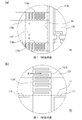
- FIG. 4 is a view showing a predetermined portion of the display panel substrate 1b according to the second embodiment of the present invention.
- 4A is an enlarged view of the portion B in FIG. 1
- FIG. 4B is an enlarged view of the portion C in FIG. That is, these drawings are plan views schematically showing the structure of the wiring formed in the panel frame region 12 of the display panel substrate 1b according to the second embodiment of the present invention.
- predetermined wiring (scanning line 116b, auxiliary capacitance signal line 118b, and data line 117b) is formed in the panel frame region 12. Specifically, as shown in FIG. 4A, scanning lines 116 b and storage capacitor signal lines 118 b are formed extending from the display area 11 on predetermined sides of the panel frame area 12. Further, as shown in FIG. 4B, data lines 117 b are formed extending from the display area 11 on other predetermined sides of the panel frame area 12. These wirings 116 b, 117 b and 118 b cross the seal pattern area 123 of the panel frame area 12 and reach the terminal area 121.
- a portion extending between the seal pattern region 123 and the display region 11 and a portion formed in the seal pattern region 123 are portions 119d formed in a zigzag manner. , 119e, 119f.
- the scanning line 116b and the auxiliary capacitance signal line 118b extending from the display region 11 have portions 119d and 119e formed in a zigzag shape.
- the portions 119d and 119e formed in a zigzag shape are parallel to the extending direction of the seal pattern region 123 where the scanning line 116b and the auxiliary capacitance signal line 118b intersect (the direction indicated by the arrow C in FIG. 4A). Has a stretched part.
- the data line 117b extending from the display area 11 also has a portion 119f formed in a zigzag shape.
- the portion 119f formed in a zigzag shape has a portion extending in parallel with the extending direction of the seal pattern region 123 where the data line 117b intersects (the direction indicated by the arrow D in FIG. 4B).
- a part formed between the display area 11 and the seal pattern area 123 and a part formed in the seal pattern area 123 are formed in a folded shape. If the portions 119d, 119e, and 119f are included, the same operation as that of the display panel substrate 1a according to the first embodiment of the present invention can be achieved in the alignment film forming step.
- the configuration including the portions 119d, 119e, and 119f formed in a zigzag shape corresponds to a configuration in which slit-like openings are formed in the wirings 116b, 117b, and 118b. Therefore, when the alignment material flowing on the surfaces of the wirings 116b, 117b, and 118b reaches the portions 119d, 119e, and 119f formed in a zigzag shape, the flow of the alignment material is blocked by the surface tension of the alignment material. As a result, the portions 119d, 119e, and 119f that are formed in a zigzag fold form an obstacle to the flow of the alignment material, and the flow of the alignment material stops.
- the portions 119d, 119e, and 119f formed in a zigzag shape include portions that extend substantially parallel to the extending direction of the seal pattern region 123 where the wirings 116b, 117b, and 118b intersect.
- this corresponds to a configuration in which slits (for example, elongated slits) extending in a direction substantially perpendicular to the flow direction of the alignment material are formed in the wirings 116b, 117b, and 118b.
- slits for example, elongated slits
- the display panel substrate 1a according to the first embodiment of the present invention and the display panel substrate 1b according to the second embodiment are different only in the shape of the wiring, so that they are formed on the photomask used.
- the same manufacturing method can be applied except for the above pattern. Therefore, it explains collectively.
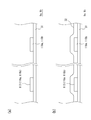
- FIG. 5 to FIG. 7 are cross-sectional views schematically showing each step of the manufacturing method of the display panel substrate 1a according to the first embodiment of the present invention and the display panel substrate 1b according to the second embodiment. It is. These cross-sectional views schematically show the cross-sectional structures of the display region 11 of the display panel substrate 1a according to the first embodiment of the present invention and the display panel substrate 1b according to the second embodiment. It is not the figure cut
- the scanning lines 116a and 116b, the auxiliary capacitance signal lines 118a and 118b, and the gate electrode 113 of the switching element 112 are formed in the display region 11 of the transparent substrate 31 made of glass or the like.
- the In the panel frame region 12, scanning lines 116a and 116b and auxiliary capacitance signal lines 118a and 118b are also formed.
- the scanning lines 116 a and 116 b and the auxiliary capacitance signal lines 118 a and 118 b formed in the panel frame region 12 are configured to extend from the display region 11.
- a single-layer or multilayer conductor film made of chromium, tungsten, molybdenum, aluminum, or the like is formed on one surface of the transparent substrate 31.
- first conductor film made of chromium, tungsten, molybdenum, aluminum, or the like is formed on one surface of the transparent substrate 31.
- Various known sputtering methods can be applied to the method for forming the first conductor film.
- the thickness of the first conductor film is not particularly limited, but for example, a film thickness of about 300 nm can be applied.
- the formed first conductor film includes scanning lines 116a and 116b, auxiliary capacitance signal lines 118a and 118b, a gate electrode 113 of the switching element 112, and the like as shown in FIG. Patterned into shape.
- Various known wet etchings can be applied to the patterning of the first conductor film.
- wet etching using (NH 4 ) 2 [Ce (NH 3 ) 6 ] + HNO 3 + H 2 O solution can be applied.
- the scanning lines 116a and 116b and the auxiliary capacitance signal lines 118a and 118b are also formed in the panel frame region 12.
- slit-shaped openings 119a and 119b or portions 119d and 119e formed in a zigzag shape are formed.
- a gate insulating film 32 is formed in the display region 11 of the transparent substrate 31 that has undergone the above-described steps.
- SiNx silicon nitride
- a plasma CVD method can be applied.
- the scanning lines 116a and 116b, the auxiliary capacitance signal lines 118a and 118b, and the gate electrode 113 of the switching element 112 are covered with the gate insulating film 32. .
- a semiconductor film 33 having a predetermined shape is formed at a predetermined position on the surface of the gate insulating film 32. Specifically, the semiconductor film 33 is formed at a position overlapping the gate electrode 113 via the gate insulating film 32 and a position overlapping the auxiliary capacitance signal lines 118 a and 118 b via the gate insulating film 32.
- the semiconductor film 33 has a two-layer structure of a first sub semiconductor film 331 and a second sub semiconductor film 332.
- amorphous silicon or the like having a thickness of about 100 nm can be used.
- n + -type amorphous silicon having a thickness of about 20 nm can be used.
- the first sub semiconductor film 331 functions as an etching stopper layer in the process of forming the data lines 117a, 117b, the drain wiring 119, and the like by etching.
- the second sub-semiconductor film 332 is for improving the ohmic contact with the source electrode 114 and the drain electrode 115 formed in a later step.
- the semiconductor film 33 (the first sub semiconductor film 331 and the second sub semiconductor film 332) can be formed by using a plasma CVD method and a photolithography method. That is, first, the material of the semiconductor film 33 (the first sub-semiconductor film 331 and the second sub-semiconductor film 332) is deposited on the one-side surface of the transparent substrate that has undergone the above-described steps, by using plasma CVD.
- the formed semiconductor film 33 (the first sub semiconductor film 331 and the second sub semiconductor film 332) is patterned into a predetermined shape by using a photolithography method or the like. Specifically, a layer of a photoresist material is formed on the surface of the formed semiconductor film 33. A spin coater or the like can be applied to form the photoresist material layer. Then, the formed photoresist material layer is exposed to light using a photomask, and then developed. Then, a layer of a photoresist material having a predetermined pattern remains on the surface of the semiconductor film 33 in the display region.
- the semiconductor film is patterned using the patterned photoresist material layer as a mask.
- the semiconductor film 33 for example, wet etching using HF + HNO 3 solution or dry etching using Cl 2 and SF 6 gas can be applied.
- the semiconductor film 33 (the first sub semiconductor film 331 and the second sub semiconductor film 332) is formed so as to overlap the gate electrode 113 with the gate insulating film 32 interposed therebetween, and the auxiliary capacitance signal line 118a. , 118b.
- the data lines 117a and 117b, the drain wiring 119, the source electrode 114 and the drain electrode 115 of the switching element 112 are formed.
- the data lines 117a and 117b, the drain wiring 119, and the conductor film that is the material of the source electrode 114 and the drain electrode 115 of the switching element 112 This is referred to as a conductor film ").
- the formed second conductive film is patterned into a predetermined shape.
- This second conductor film has a laminated structure of two or more layers made of titanium, aluminum, chromium, molybdenum or the like.
- the second conductor film has a two-layer structure. That is, the second conductor film has a two-layer structure including a first sub conductor film on the side close to the transparent substrate 31 and a second sub conductor film on the side close to the pixel electrode. Titanium or the like can be applied to the first sub conductor film. Aluminum or the like can be applied to the second sub conductor film.
- a sputtering method or the like can be applied as a method for forming the second conductor film.
- a sputtering method or the like For the patterning of the second conductor film, dry etching using Cl 2 and BCl 3 gas and wet etching using phosphoric acid, acetic acid, and nitric acid can be applied.
- the data lines 117a and 117b, the drain wiring 119, the source electrode 114 and the drain electrode 115 of the switching element 112 are formed.
- the second sub semiconductor film is also etched using the first sub semiconductor film as an etching stopper layer.
- the display area of the transparent substrate 31 includes the switching element 112 (that is, the gate electrode 113, the source electrode 114, and the drain electrode 115), the data lines 117a, 117b, Scan lines 116a and 116b, drain wiring 119, and auxiliary capacitance signal lines 118a and 118b are formed.
- the data lines 117a and 117b are formed with slit-like openings 119c or zigzag-folded portions 119f between the display area 11 and the seal pattern area 123 and in the seal pattern area 123. .
- a passivation film 34 and an organic insulating film 35 are formed in the display region 11 of the transparent substrate 31 that has undergone the above-described steps.
- SiNx silicon nitride
- As a method of forming the passivation film 34 a plasma CVD method or the like can be applied.
- An organic insulating film 35 is formed on the surface of the formed passivation film 34.
- An acrylic resin material can be applied to the organic insulating film 35.
- the formed organic insulating film 35 is patterned into a predetermined pattern by a photolithography method or the like. By this patterning, an opening (contact hole) 351 for electrically connecting the pixel electrode 111 and the drain wiring 119 is formed in the organic insulating film 35.
- the passivation film 34 is patterned using the patterned organic insulating film 35 as a mask.
- the pixel electrode 111 is formed in the display area 11.
- ITO IndiumideTin Oxide
- various known sputtering methods can be applied as a method for forming the pixel electrode 111.
- the display panel substrate 1a according to the first embodiment of the present invention and the display panel substrate 1b according to the second embodiment are manufactured.
- the display panel manufacturing method includes a TFT array substrate manufacturing process, a color filter manufacturing process, and a panel (cell) manufacturing process.
- the TFT array substrate manufacturing process is as described above.
- FIG. 8 is a diagram schematically showing the configuration of the counter substrate 5. Specifically, FIG. 8A is a perspective view schematically showing the entire structure of the counter substrate 5, and FIG. FIG. 8C is a cross-sectional view taken along the line FF of FIG. 8B and shows the cross-sectional structure of the picture element.
- FIG. 8A is a perspective view schematically showing the entire structure of the counter substrate 5
- FIG. 8C is a cross-sectional view taken along the line FF of FIG. 8B and shows the cross-sectional structure of the picture element.
- FIG. 8A is a perspective view schematically showing the entire structure of the counter substrate 5
- FIG. 8C is a cross-sectional view taken along the line FF of FIG. 8B and shows the cross-sectional structure of the picture element.
- the counter substrate 5 has a black matrix 52 formed on one surface of a transparent substrate 51 made of glass or the like, and red, green, and blue colors are arranged inside each lattice of the black matrix 52.
- a colored layer 53 made of the colored sensitizing material is formed.
- the grids on which the colored layers 53 of these colors are formed are arranged in a predetermined order.
- a protective film 54 is formed on the surface of the black matrix 52 and the colored layer 53 of each color, and a transparent electrode (common electrode) 55 is formed on the surface of the protective film 54.
- an alignment regulating structure 56 that controls the alignment of the liquid crystal is formed.
- the color filter manufacturing process includes a black matrix forming process, a colored layer forming process, a protective film forming process, and a transparent electrode (common electrode) forming process.
- the contents of the black matrix forming step are as follows for the resin BM method, for example.
- a BM resist (referred to as a photosensitive resin composition containing a black colorant) or the like is applied to the surface of the transparent substrate 51.
- the applied BM resist is formed into a predetermined pattern using a photolithography method or the like. Thereby, a black matrix 52 having a predetermined pattern is obtained.
- the color sensitive material method is as follows. First, a colored light-sensitive material (referred to as a solution in which a pigment of a predetermined color is dispersed in a photosensitive material) is applied to the surface of the transparent substrate 51 on which the black matrix 52 is formed. Next, the applied colored light-sensitive material is formed into a predetermined pattern using a photolithography method or the like. This step is performed for each color of red, green, and blue. Thereby, the colored layer 53 of each color is obtained.
- a colored light-sensitive material referred to as a solution in which a pigment of a predetermined color is dispersed in a photosensitive material
- the method used in the black matrix forming step is not limited to the resin BM method.
- various known methods such as a chromium BM method and a superposition method can be applied.
- the method used in the colored layer forming step is not limited to the colored photosensitive material method.
- various known methods such as printing, dyeing, electrodeposition, transfer, and etching can be applied.
- a back exposure method in which a colored layer is formed first and then a black matrix is formed may be used.
- a protective film 54 is formed on the surfaces of the black matrix 52 and the colored layer 53.
- a protective film having a predetermined pattern is formed on the surface of the transparent substrate 51 that has undergone the above-described process by using a method (full surface coating method) in which a protective film material is applied using a spin coater, printing, or photolithography. A method (patterning method) or the like can be applied.
- the protective film material for example, an acrylic resin or an epoxy resin can be applied.
- a transparent electrode (common electrode) 55 is formed on the surface of the protective film 54.
- a mask is disposed on the surface of the transparent substrate 51 that has undergone the above-described process, and indium tin oxide (ITO) is deposited by sputtering or the like to form a transparent electrode (common electrode) 55.
- ITO indium tin oxide
- This alignment regulating structure 56 is made of, for example, a photosensitive resin material or the like, and is formed using a photolithography method or the like. A photosensitive material is applied to the surface of the transparent substrate 51 that has undergone the above-described process, and is exposed to a predetermined pattern through a photomask. Then, unnecessary portions are removed in the subsequent development process, and the alignment regulating structure 56 having a predetermined pattern is obtained.
- the counter substrate 5 is obtained through such steps.
- FIG. 9 is a cross-sectional view schematically showing a partial cross-sectional structure of the display panel 6 according to the embodiment of the present invention.
- the display panel 6 according to the embodiment of the present invention is opposite to the display panel substrate 1a according to the first embodiment of the present invention or the display panel substrate 1b according to the second embodiment.
- a substrate (color filter) 5 are arranged to face each other with a predetermined minute interval.
- a seal material is applied to the seal pattern region 123 of the display panel substrates 1a and 1b according to the embodiment of the present invention, and a seal 63 is formed so as to surround the display region 11 with the applied seal material.
- the display panel substrates 1a and 1b and the counter substrate (color filter) 5 according to the embodiment of the present invention are bonded and fixed by the seal 63, and the liquid crystal is sealed in a region surrounded by the seal 63.
- the alignment film 61, the TFT array substrate (ie, the display panel substrates 1 a and 1 b according to any embodiment of the present invention) and the counter substrate (color filter) 5 obtained through the above-described steps are formed on the respective surfaces. 62 is formed. Then, alignment treatment is performed on the formed alignment films 61 and 62. Thereafter, the display panel substrates 1a and 1b and the counter substrate 5 according to the embodiment of the present invention are bonded together, and liquid crystal is filled between them.
- the method for forming the alignment films 61 and 62 on the surfaces of the display panel substrates 1a and 1b and the counter substrate 5 according to the embodiment of the present invention is as follows. First, an alignment material is applied to the surfaces of the display regions of the display panel substrates 1a and 1b and the counter substrate 5 according to the embodiment of the present invention using an alignment material application device or the like.
- the alignment material refers to a solution containing a material that is a raw material for the alignment film.
- An ink jet printing apparatus (dispenser) can be applied to the alignment material coating apparatus.
- the ones riding on the surfaces of the wirings 116a, 116b, 117a, 117b, 118a, and 118b flow along the wirings 116a, 116b, 117a, 117b, 118a, and 118b and try to spread out.
- the wirings 116 a, 116 b, 117 a, 117 b, 118 a, and 118 b extending from the display area 11 and reaching the seal pattern area 123 include the space between the display area 11 and the seal pattern area 123 and the seal pattern area 123.
- slit-shaped openings 119a, 119b, and 119c or portions 119d, 119e, and 119f formed in a zigzag shape are formed. These slit-shaped openings 119a, 119b, and 119c and the portions 119d, 119e, and 119f formed in a zigzag shape prevent the alignment material from flowing.
- the alignment material dropped on the wirings 116a, 116b, 117a, 117b, 118a, 118b is prevented from reaching the seal pattern region 123 through the wirings 116a, 116b, 117a, 117b, 118a, 118b. can do. Further, even when the alignment material reaches the seal pattern region 123, it can be prevented that the alignment material spreads over the entire region of the seal pattern region 123 or crosses the seal pattern region 123 and reaches the outside of the seal pattern region 123. As a result, the alignment film 61 can be prevented from being formed outside the seal pattern region 123 or the seal pattern region 123.
- the applied alignment materials 61 and 62 are heated and baked using an alignment film baking apparatus or the like.
- alignment treatment is performed on the fired alignment films 61 and 62.
- this alignment treatment there are a method of scratching the surface of the alignment film using a rubbing roll, etc. Various known processing methods can be applied. Moreover, the structure which does not perform an orientation process may be sufficient.
- a seal material is applied to the seal pattern region 123 of the display panel substrates 1a and 1b according to the embodiment of the present invention using a seal patterning device or the like.
- spacers for keeping the cell gap uniform at a predetermined value are dispersed on the surfaces of the display panel substrates 1a and 1b according to the embodiment of the present invention by using a spacer dispersion device or the like. And using a liquid crystal dropping device etc., a liquid crystal is dripped at the area
- the display panel substrates 1a and 1b and the counter substrate 5 are bonded together in a reduced pressure atmosphere according to any of the embodiments of the present invention.
- the sealing material is irradiated with ultraviolet rays to solidify the sealing material.
- the liquid crystal may be injected between the display panel substrate and the counter substrate (color filter) according to any one of the embodiments of the present invention.
- the display panel according to the embodiment of the present invention is obtained.
Landscapes
- Physics & Mathematics (AREA)
- Nonlinear Science (AREA)
- Engineering & Computer Science (AREA)
- Microelectronics & Electronic Packaging (AREA)
- Mathematical Physics (AREA)
- Chemical & Material Sciences (AREA)
- Crystallography & Structural Chemistry (AREA)
- General Physics & Mathematics (AREA)
- Optics & Photonics (AREA)
- Devices For Indicating Variable Information By Combining Individual Elements (AREA)
Abstract
インクジェット方式の印刷機を用いて配向膜を形成する構成において、滴下した配向材がシールパターン領域に流出しないような表示パネル用の基板および表示パネルを提供すること。 複数の絵素電極111がマトリックス状に配列される表示領域11と、表示領域11を囲繞するように形成されるシールパターン領域123と、表示領域11内に配列される所定の絵素に所定の信号を伝送することができる配線116a,117a,118aとを備え、配線116a,117a,118aのうちの表示領域11とシールパターン領域123との間の領域に形成される部分およびシールパターン領域123に形成される部分には、近接するシールパターン領域123の延伸方向に略平行に延伸するスリット状の開口部119a,119b,119cが形成される。
Description
本発明は、表示パネル用の基板および表示パネルに関するものであり、特に、液晶表示パネルに好適な表示パネル用の基板と、この表示パネル用の基板を備える表示パネルに関するものである。
一般的な液晶表示パネルは、二枚の基板を備える。たとえば、アクティブマトリックスタイプの液晶表示パネルであれば、TFTアレイ基板と対向基板(たとえばカラーフィルタなど)とを備える。そして、これらの基板が、所定の微小な間隔をおいて対向して配設され、これらの基板の間に液晶が充填されるという構成を備える。充填された液晶は、絵素が配列される領域を囲繞するように形成されるシール材によって封止される。換言すると、シール材に囲繞される領域に、液晶が充填される。
TFTアレイ基板の片側表面には、薄膜トランジスタ、データ線(ソース配線とも称する)、走査線(ゲート配線とも称する)、半導体膜、絵素電極などといった、様々な配線パターンや薄膜パターンが形成される。そして絵素電極の表面の最上層には、液晶の配向を規制する機能を有する配向膜が形成される。また、カラーフィルタの片側表面には、ブラックマトリックス、着色層、共通電極などといった所定の薄膜パターンや配線パターンなどが形成される。そして共通電極の表面の所定の領域には、液晶の配向を規制する機能を有する配向膜が形成される。
そして、TFTアレイ基板またはカラーフィルタの一方に、配向膜が形成された領域を囲繞するようにシール材が塗布され、二枚の基板が貼り合わされる。すなわち、TFTアレイ基板、対向基板(カラーフィルタ)ともに、貼り合わされた状態において、配向膜が形成される領域を囲繞するようにシール材が形成されることになる。
配向膜の形成には、輪転機などの印刷機を用いる方法が広く用いられている。輪転機を用いる配向膜の形成方法は、印刷ローラ(印刷版)に配向材(配向膜の材料となる溶液)を塗布し、塗布された配向材を、表示パネル用の基板の表面の所定の領域に転写するというものである。このような方法によれば、表示パネル用の基板の表面の所定の領域に、精度良く配向材を転写(塗布)することができるという利点を有する。一方で、表示パネル用の基板の種類ごとに(特に、画面サイズごとに)、専用の印刷ローラが必要となるという問題点を有する。すなわち、表示パネル用の基板の種類に応じた印刷ローラが必要となるため、製造コストの削減が困難である。また、製造する表示パネル用の基板の種類を変更するたびに、印刷機の印刷ローラを変更する必要があるため、設備の柔軟性が低いという問題点もある。
このため近年では、インクジェット方式の印刷機を用いて配向膜を形成するという方法が採用されるようになってきている。インクジェット方式の印刷機によれば、配向材の滴下位置や滴下範囲を容易に変更することができる。このため、一台の印刷機で様々な種類の表示パネル用の基板に対応することができる。したがって、従来のように表示パネル用の基板の種類ごとに印刷ローラを用意する必要がなく、また製造機種変更のたびに印刷ローラを変更するという手間を省略することができる。このように、インクジェット方式の印刷機によれば、設備コストの削減を図ることができるとともに、設備の柔軟性の向上を図ることができる。
ところで、インクジェット方式の印刷機は、滴下ノズルを備え、この滴下ノズルが配向材を表示パネル用の基板の表面の所定の位置に滴下する。滴下された配向材は、表示パネル用の基板の表面を濡れ拡がっていく。そして濡れ拡がった配向材どうしが繋がっていくことにより、表示パネル用の基板の表面の所定の領域に、配向材の層が形成される。
前記のようにシール材は、配向膜が形成される領域を囲繞するように形成される。そしてシール材は、配向膜の表面には形成されない。しかしながら濡れ拡がった配向材がシール材を形成すべき位置にまで達して、シール材を形成すべき位置に配向膜が形成されると、次のような問題が発生することがある。
シール材は、二枚の基板の間に充填される液晶を密封する機能を有する。このためシール材は、表示パネル用の基板の表面に強固に密着していることが好ましい。しかしながら、一般的に配向膜とシール材とは密着性が低いため、シール材が形成される位置に配向膜が形成されると(換言すると、配向膜の表面にシール材が形成される構造となると)、液晶を密封する機能が低下するおそれがある。また、配向膜は一般的にポリイミドにより形成される。ポリイミドは吸湿性が高い材料であるため、配向膜がシール材の外側に露出すると、この露出した配向膜を通じて、液晶が密封される領域の内部に水分が滲入するおそれがある。
上記実情に鑑み、本発明が解決しようとする課題は、インクジェット方式の印刷機によって配向膜を塗布する場合において、滴下された配向材が、本来濡れ拡がるべきではない方向に拡がらないようにすることができる表示パネル用の基板およびこの基板を備える表示パネルを提供すること、特に、滴下された配向材が、シールパターン領域に濡れ拡がらないようにすることができる表示パネル用の基板およびこの基板を備える表示パネルを提供すること、または、滴下された配向材が、シールパターン領域を越えて濡れ拡がらないようにすることができる表示パネル用の基板およびこの基板を備える表示パネルを提供すること、または、シール材による液晶の密封の度合を維持することができる表示パネル用の基板およびこの基板を備える表示パネルを提供することである。
前記課題を解決するため、本発明は、複数の絵素電極がマトリックス状に配列される表示領域と、該表示領域を囲繞するように形成されるシールパターン領域と、前記表示領域内に配列される所定の絵素に所定の信号を伝送することができる配線と、を備え、前記配線のうちの前記表示領域と前記シールパターン領域との間の領域に形成される部分には開口部が形成されることを要旨とするものである。
前記開口部は、近接するシールパターン領域の延伸方向に略平行に延伸するスリット状に形成されることが好ましい。
本発明は複数の絵素電極がマトリックス状に配列される表示領域と、該表示領域を囲繞するように形成されるシールパターン領域と、前記表示領域内に配列される所定の絵素に所定の信号を伝送することができる配線と、を備え、前記配線のうちの前記シールパターン領域に形成される部分には開口部が形成されることを要旨とするものである。
前記開口部は、近接するシールパターン領域の延伸方向に略平行に延伸するスリット状に形成されることが好ましい。
本発明は、複数の絵素電極がマトリックス状に配列される表示領域と、該表示領域を囲繞するように形成されるシールパターン領域と、前記表示領域内に配列される所定の絵素に所定の信号を伝送することができる配線と、を備え、前記配線のうちの前記表示領域と前記シールパターン領域との間の領域に形成される部分にはつづら折り状に形成される部分を有することを要旨とするものである。
前記つづら折り状に形成される部分には、近接するシールパターン領域の延伸方向に略平行に延伸する部分が含まれることが好ましい。
本発明は、複数の絵素電極がマトリックス状に配列される表示領域と、該表示領域を囲繞するように形成されるシールパターン領域と、前記表示領域内に配列される所定の絵素に所定の信号を伝送することができる配線と、を備え、前記配線のうちの前記シールパターン領域に形成される部分にはつづら折り状に形成される部分を有することを要旨とするものである。
前記つづら折り状に形成される部分には、近接するシールパターン領域の延伸方向に略平行に延伸する部分が含まれることが好ましい。
前記配線にはデータ線が好適に適用できる。また、前記配線には走査線が好適に適用できる。
本発明に係る表示パネルは、前記表示パネル用の基板と、対向基板とを備えることを要旨とするものである。
本発明によれば、インクジェット方式の印刷機を用いて配向膜を形成する構成において、滴下された配向材は表示パネル用の基板に形成される配線に沿って流動しようとするが、配線に形成される開口部が、配向材の流動を阻止する。したがって、絵素が配列される領域に滴下された配向材が、配線を伝ってシールパターン領域に流出することが防止される。このため、シール材を形成する工程において、シール材が配向膜に接触すること(シール材が配向膜の表面に形成されること)が防止される。このような構成であれば、表示パネル用の基板とシール材との密着性を維持することができる。
また、本発明によれば、絵素が配列される領域に滴下された配向材が、配線を伝ってシールパターン領域の外側に流出することが防止される。このため、配向膜がシールパターン領域の外側に形成されることが防止される。したがって、配向膜が外気に露出しなくなるから、外気中の水分が配向膜を通じて液晶中に滲入することが防止される。
ここで、配線に形成される開口部が、近接するシールパターン領域の延伸方向に略平行な方向に延伸するものであれば、滴下された配向材の流動を、より効果的に防止することができる。
また、本発明によれば、インクジェット方式の印刷機を用いて配向膜を形成する構成において、滴下された配向材は表示パネル用の基板に形成される配線を伝って流動しようとするが、配線に形成されるつづら折り状の部分が、配向材の流動を阻止する。したがって、前記同様の作用効果を奏することができる。
ここで、つづら折り状の部分が、近接するシールパターン領域の延伸方向に略平行な方向に延伸する部分を有するものであれば、滴下された配向材の流動を、より効果的に防止することができる。
以下に、本発明の各種実施形態について、図面を参照して詳細に説明する。本発明の各実施形態にかかる表示パネル用の基板は、アクティブマトリックスタイプの液晶表示パネルに適用されるTFTアレイ基板である。
図1は、本発明の第一実施形態にかかる表示パネル用の基板1aおよび第二実施形態にかかる表示パネル用の基板1bの概略構成を、模式的に示した外観斜視図である。まず、図1を参照して、本発明の第一実施形態にかかる表示パネル用の基板1aおよび第二実施形態にかかる表示パネル用の基板1bの全体的な構成を説明する。なお、第一実施形態にかかる表示パネル用の基板1aと、第二実施形態にかかる表示パネル用の基板1bの全体構成は、ほぼ同じであることから、まとめて説明する。
図1に示すように、本発明の第一実施形態にかかる表示パネル用の基板1aおよび第二実施形態にかかる表示パネル用の基板1bは、表示領域11(アクティブ領域とも称する)が設けられる。そして、表示領域11の外側には、この表示領域11を囲繞するように、パネル額縁領域12が設けられる。
図2は、表示領域11に設けられる絵素と配線の構成を、模式的に示した平面図である。図2に示すように表示領域11には、複数の絵素がマトリックス状に配列される。各絵素は、絵素電極111と、この絵素電極111を駆動するスイッチング素子112(具体的にはたとえば薄膜トランジスタ(TFT:Thin Film Transistor)を有する。そしてスイッチング素子112のドレイン電極115と絵素電極111とがドレイン配線119により電気的に接続されている。また、表示領域11には、複数の走査線116a,116b(ゲート配線とも称する)が、互いに略平行に設けられる。そして、走査線116a,116bどうしの間には、補助容量信号線118a,118b(蓄積容量信号線とも称する)が、走査線116a,116bに略平行に設けられる。さらに、複数のデータ線117a,117b(ソース配線とも称する)が、互いに略平行で、かつ走査線116a,116bおよび補助容量信号線118a,118bに略直交するように設けられる。
各走査線116a,116bは、所定の複数の絵素のスイッチング素子112のゲート電極113に、電気的に接続されている。そして各走査線116a,116bは、これらの所定のスイッチング素子112のゲート電極113に、ゲート信号(選択パルスとも称する)を伝送することができる。補助容量信号線118a,118bは、所定の絵素電極111との間に補助容量(蓄積容量とも称する)を形成する。データ線117a,117bは、所定の複数の絵素のスイッチング素子112のソース電極114に電気的に接続されている。そしてデータ線117a,117bは、これら所定のスイッチング素子112のソース電極114に、データ信号を伝送することができる。
図1に戻って説明する。表示領域11の周囲には、この表示領域11を囲繞するように、パネル額縁領域12が設けられる。このパネル額縁領域12には、端子領域121が設けられるとともに、シールパターン領域123が設定される。
端子領域121は、パネル額縁領域12の外周縁または外周縁近傍に設けられる領域である。この端子領域121には、配線電極端子122が設けられる。この配線電極端子122は、表示領域11から延設される所定の配線(走査線116a,116b、補助容量信号線118a,118b、データ線117a,117bなど)と、ドライバIC(ドライバLSIとも称する)とを接続するための端子である。具体的には、端子領域121に異方性導電膜(ACF:Anisotropic Conductive Film)が貼付され、ドライバIC(またはドライバLSI)が実装されたTCP(Tape Carrier Package)が、貼付された異方性導電膜によって、配線電極端子122に固定される。このような構成によれば、TCPに実装されるドライバICなどが生成した所定の信号は、配線電極端子122を通じて、表示領域11に設けられる所定の配線(走査線116a,116b、補助容量信号線118a,118b、データ線117a,117b)に伝送することができる。
パネル額縁領域12には、シールパターン領域123が設定される。シールパターン領域123は、液晶を封止保持するためのシールパターンが形成される領域(換言すると、シール材が塗布される領域)である。シールパターンは、本発明の第一実施形態にかかる表示パネル用の基板1aまたは第二実施形態にかかる表示パネル用の基板1bと、対向基板とが貼り合わされた状態において、本発明の第一実施形態にかかる表示パネル用の基板1aまたは本発明の第二実施形態にかかる表示パネル用の基板1bと対向基板との間に、液晶を封入するとともに(換言すると液晶層を形成するとともに)、対向基板を本発明の第一実施形態にかかる表示パネル用の基板1aまたは第二実施形態にかかる表示パネル用の基板1bに固定する。図1に示すように、シールパターン領域123は、表示領域11の外周縁から所定の距離をおいて、この表示領域11を囲繞するように設定される領域である。具体的にはシールパターン領域123は、開口した略四辺形を有する額縁状の領域であり、四辺形の各辺は所定の幅寸法を有する。
図3は、本発明の第一実施形態にかかる表示パネル用の基板1aの所定の部分を抜き出して示した図である。それぞれ図3(a)は、図1のB部を抜き出して拡大して示した図、図3(b)は、図1のC部を抜き出して拡大して示した図である。すなわちこれらの図は、本発明の第一実施形態にかかる表示パネル用の基板1aのパネル額縁領域12に形成される配線の構造を、模式的に示した平面図である。
図3(a),(b)のそれぞれに示すように、パネル額縁領域12には、所定の配線(走査線116a、補助容量信号線118a、データ線117a)が形成される。具体的には、図3(a)に示すように、パネル額縁領域12の所定の辺には、走査線116aと補助容量信号線118aが、表示領域11から延伸して形成される。また、図3(b)に示すように、パネル額縁領域12の他の所定の辺には、データ線117aが、表示領域11から延伸して形成される。これらの配線116a,117a,118aは、パネル額縁領域12のシールパターン領域123を横断し、端子領域121に達する。
これら所定の配線116a,117a,118aのうち、シールパターン領域123と表示領域11との間に延設される部分およびシールパターン領域123に形成される部分には、スリット状の開口部119a,119b,119cが形成される。具体的には図3(a)に示すように、表示領域11から延伸する走査線116aおよび補助容量信号線118aに、スリット状の開口部119a,119bが形成される。このスリット状の開口部119a,119bは、走査線116aおよび補助容量信号線118aが交差するシールパターン領域123の延伸方向(図3(a)においては、矢印Aで示す方向)に細長い形状を有する。このため走査線116aおよび補助容量信号線118aは、表示領域11とシールパターン領域123との間に延設される部分およびシールパターン領域123に形成される部分は、全体としてはしご状の構造を有する。
また、図3(b)に示すように、表示領域11から延伸するデータ線117aに、スリット状の開口部119cが形成される。このスリット状の開口部119cは、データ線117aが交差するシールパターン領域123の延伸方向(図3(b)においては、矢印Bで示す方向)に細長い形状を有する。したがってデータ線117aは、走査線116aおよび補助容量信号線118aと同様に、表示領域11とシールパターン領域123との間に延設される部分およびシールパターン領域123に形成される部分は、全体としてはしご状の構造を有する。
表示領域11から延伸してシールパターン領域123を横断する配線のうち、表示領域11とシールパターン領域123との間およびシールパターン領域123に形成される部分にスリット状の開口部119a,119b,119cが形成されると、配向膜の形成工程において次のような作用を奏する。配向膜は、液晶の配向を規制する機能を有する膜であり、表示領域11(すなわち絵素電極の表面)に形成される。
配向膜の形成は、まずインクジェット方式の印刷機を用いて、本発明の第一実施形態にかかる表示パネル用の基板1aの表示領域11の表面に、配向材の滴を滴下する。配向材とは、配向膜の原料を溶解した溶液をいうものとする。滴下された配向材の滴は、それが有する濡れ性および流動性によって濡れ拡がっていく。そして濡れ拡がった配向材の滴どうしが繋がっていく。これにより、表示領域11の表面に、配向材の膜が形成される。そして形成された配向材の膜を焼成することによって、配向材に含まれる揮発成分を除去して固化させる。これにより、表示領域11の表面に配向膜が形成される。
滴下された配向材の滴や、濡れ拡がった配向材の滴のうち、表示領域11に形成される配線(走査線116a、補助容量信号線118a、データ線117a)の表面に乗ったものは、これらの配線116a,117a,118aの表面を伝わるように流動する。すなわち、配線116a,117a,118aの表面に乗った配向材は、当該配線116a,117a,118aの表面を、その延伸方向に流れる。ここで、配線116a,117a,118aにスリット状の開口部119a,119b,119cが形成されると、これらのスリット状の開口部119a,119b,119cが、配向材の流動を防止する機能を果たす。具体的には、配線116a,117a,118aの表面を流れる配向材が、スリット状の開口部119a,119b,119cが形成される部分に達すると、スリット状の開口部119a,119b,119cの端縁において配向材の表面張力により、流動が阻止される。この結果、スリット状の開口部119a,119b,119cが配向材の流動の障碍物となり、配向材の流動が停止する。
特に、これらのスリット状の開口部119a,119b,119cは、配線116a,117a,118aが交差するシールパターン領域123の延伸方向に、略平行に形成される。これは換言すると、これらのスリット状の開口部119a,119b,119cは、配線116a,117a,118aに乗った配向材の流動方向に略直角な方向に延伸する。したがって、このような構成によれば、シールパターン領域123に向かって流れる配向材の流動や、シールパターン領域123に到達した配向材がさらにシールパターン領域123の全域に広がることやシールパターン領域123を横断してシールパターン領域123の外側に到達することを、より効果的に阻止することができる。
これらのスリット状の開口部119a,119b,119cが表示領域11とシールパターン領域123との間に形成されると、表示領域11とシールパターン領域123との間に、配向材の流動を阻止する障碍物が形成されたのと同様の作用を奏する。したがって、表示領域11に滴下された配向材が、表示領域11から延伸する配線116a,117a,118aを伝わって、シールパターン領域123に流入することを防止できる。この結果、シールパターン領域123の表面に、配向膜が形成されることを防止できる。同様に、配向材がシールパターン領域123の外側にまで達するように形成されること(換言すると、配向膜が表示領域11からシールパターン領域123の外側に跨って形成されること)を防止できる。
また、スリット状の開口部119a,119b,119cがシールパターン領域123に形成されると、シールパターン領域123に、配向材の流動を阻止する障碍物が形成されたのと同様の作用を奏する。したがって、表示領域11に滴下された配向材が、表示領域11から延伸する配線116a,117a,118aを伝わってシールパターン領域123に到達したとしても、配向材がシールパターン領域123の全域にわたって広がることを防止または抑制できる。この結果、シールパターン領域123の表面に、配向膜が形成されることを防止または抑制できる。同様に、配向材がシールパターン領域123の外側にまで達するように形成されること(換言すると、配向膜が表示領域11からシールパターン領域123の外側に跨って形成されること)を防止できる。
配向膜を形成した後、シールパターン領域123にはシールパターンが形成される。シールパターンは、たとえば紫外線硬化型の樹脂材料により形成される。具体的には、シール材塗布装置(たとえばディスペンサなど)により、シールパターン領域123の表面にシール材が塗布される。シール材は、公知の各種シール材が適用できる。たとえば紫外線硬化型のシール材が好適に適用できる。その後、本発明の第一実施形態にかかる表示パネル用の基板1aと対向基板とが貼り合わされる。そして、シール材に紫外線が照射され、シール材を固化させる。これにより、表示領域11を囲繞するように、シールパターンが形成される。
シールパターンは、シールパターンに囲まれる領域の内側に液晶を密封する機能を有する。また、本発明の第一実施形態にかかる表示パネル用の基板1aに、対向基板を接着固定する機能を有する。したがって、シール材は、本発明の第一実施形態にかかる表示パネル用の基板1aの表面に、強固に密着している必要がある。ところで一般的に、配向膜とシール材とは密着性が低い。したがって、シールパターン領域123の表面とシール材との密着性を確保するためには、シールパターン領域123の表面に配向膜が形成されないようにする必要がある。
本発明の第一実施形態にかかる表示パネル用の基板1aによれば、前記の通り配向膜の形成工程において、シールパターン領域123に配向膜が形成されることを防止できる。したがって、シール材と本発明の第一実施形態にかかる表示パネル用の基板1aの表面との密着性を損なうことがない。
また、本発明の第一実施形態にかかる表示パネル用の基板1aによれば、配向膜をシールパターン領域123の内側にのみ形成することができる。すなわち、シールパターンを形成した後において、配向膜が、シールパターンに囲まれる領域(密閉された領域)と外気との間に跨って形成されることを防止できる。したがって、外気中の水分が、配向膜を通じてシールパターンに囲まれる領域に滲入することを防止できる。
次いで、本発明の第二実施形態にかかる表示パネル用の基板1bについて説明する。図4は、本発明の第二実施形態にかかる表示パネル用の基板1bの所定の部分を抜き出して示した図である。それぞれ図4(a)は、図1のB部を抜き出して拡大して示した図、図4(b)は、図1のC部を抜き出して拡大して示した図である。すなわちこれらの図は、本発明の第二実施形態にかかる表示パネル用の基板1bのパネル額縁領域12に形成される配線の構造を、模式的に示した平面図である。
図4(a),(b)のそれぞれに示すように、パネル額縁領域12には、所定の配線(走査線116b、補助容量信号線118b、データ線117b)が形成される。具体的には、図4(a)に示すように、パネル額縁領域12の所定の辺には、走査線116bと補助容量信号線118bが、表示領域11から延伸して形成される。また、図4(b)に示すように、パネル額縁領域12の他の所定の辺には、データ線117bが、表示領域11から延伸して形成される。これらの配線116b,117b,118bは、パネル額縁領域12のシールパターン領域123を横断し、端子領域121に達する。
これら所定の配線116b,117b,118bのうち、シールパターン領域123と表示領域11との間に延設される部分およびシールパターン領域123に形成される部分には、つづら折り状に形成される部分119d,119e,119fを有する。具体的には図4(a)に示すように、表示領域11から延伸する走査線116bおよび補助容量信号線118bが、つづら折り状に形成される部分119d,119eを有する。このつづら折り状に形成される部分119d,119eは、走査線116bおよび補助容量信号線118bが交差するシールパターン領域123の延伸方向(図4(a)においては、矢印Cで示す方向)に平行に延伸する部分を有する。
また、図4(b)に示すように、表示領域11から延伸するデータ線117bも、つづら折り状に形成される部分119fを有する。このつづら折り状に形成される部分119fは、データ線117bが交差するシールパターン領域123の延伸方向(図4(b)においては、矢印Dで示す方向)に平行に延伸する部分を有する。
表示領域11から延伸してシールパターン領域123を横断する配線のうち、表示領域11とシールパターン領域123との間に形成される部分およびシールパターン領域123に形成される部分につづら折り状に形成される部分119d,119e,119fが含まれると、配向膜の形成工程において本発明の第一実施形態にかかる表示パネル用の基板1aと同様の作用を奏することができる。
すなわち、つづら折り状に形成される部分119d,119e,119fを含む構成は、配線116b,117b,118bにスリット状の開口部が形成された構成に相当する。したがって、配線116b,117b,118bの表面を流れる配向材が、つづら折り状に形成される部分119d,119e,119fに達すると、配向材の表面張力により、配向材の流動が阻止される。この結果、つづら折り状に形成される部分119d,119e,119fが配向材の流動の障碍物となり、配向材の流動が停止する。
特に、これらのつづら折り状に形成される部分119d,119e,119fには、配線116b,117b,118bが交差するシールパターン領域123の延伸方向に略平行に延伸する部分が含まれる。これは換言すると、配線116b,117b,118bに、配向材の流動方向に略直角な方向に延伸するスリット(たとえば細長いスリット)が形成される構成に相当する。そしてこのような複数のスリットが、配向材の流動方向に沿って連続的に形成されることになる。したがって、このような構成によれば、シールパターン領域123に向かって流れる配向材の流動や、シールパターン領域123に到達した配向材がさらにシールパターン領域123の全域に広がることやシールパターン領域123を横断してシールパターン領域123の外側に到達することを、より効果的に阻止することができる。
次に、本発明の第一実施形態にかかる表示パネル用の基板1aおよび第二実施形態にかかる表示パネル用の基板1bの製造方法について説明する。なお、第一実施形態にかかる表示パネル用の基板1aと、第二実施形態にかかる表示パネル用の基板1bとは、配線の形状が相違するのみであるから、使用するフォトマスク(に形成されるパターン)を除いて、同じ製造方法が適用できる。したがってまとめて説明する。
図5から図7は、本発明の第一実施形態にかかる表示パネル用の基板1aおよび第二実施形態にかかる表示パネル用の基板1bの製造方法の各工程を、模式的に示した断面図である。なお、これらの断面図は、本発明の第一実施形態にかかる表示パネル用の基板1aおよび第二実施形態にかかる表示パネル用の基板1bの表示領域11の断面構造を模式的に示した図であり、特定の断面線に沿って切断した図ではない。
まず、図5(a)に示すように、ガラスなどからなる透明基板31の表示領域11に、走査線116a,116b、補助容量信号線118a,118b、およびスイッチング素子112のゲート電極113が形成される。また、パネル額縁領域12にも、走査線116a,116b、補助容量信号線118a,118bが形成される。これらのパネル額縁領域12に形成される走査線116a,116b、補助容量信号線118a,118bは、表示領域11から延伸するという構成を有する。
具体的には、透明基板31の片側表面に、クロム、タングステン、モリブデン、アルミニウムなどからなる単層または多層の導体膜(第一の導体膜)が形成される。この第一の導体膜の形成方法には、公知の各種スパッタリング法などが適用できる。また、この第一の導体膜の厚さは特に限定されるものではないが、たとえば300nm程度の膜厚が適用できる。
そして、形成された第一の導体膜が、表示領域においては、図5(a)に示すように、走査線116a,116b、補助容量信号線118a,118b、スイッチング素子112のゲート電極113などの形状にパターニングされる。この第一の導体膜のパターニングには、公知の各種ウェットエッチングが適用できる。第一の導体膜がクロムからなる構成においては、(NH4)2[Ce(NH3)6]+HNO3+H2O液を用いたウェットエッチングが適用できる。
このパターニングにおいて、パネル額縁領域12にも走査線116a,116bおよび補助容量信号線118a,118bが形成される。そして、これらパネル額縁領域12に形成される走査線116a,116bおよび補助容量信号線118a,118bのうち、表示領域11とシールパターン領域123との間の領域に形成される部分およびシールパターン領域123に形成される部分には、スリット状の開口部119a,119bまたはつづら折り状に形成される部分119d,119eが形成される。
次に、図5(b)に示すように、前記工程を経た透明基板31の表示領域11には、ゲート絶縁膜32が形成される。ゲート絶縁膜32には、厚さ300nm程度のSiNx(窒化シリコン)などが適用できる。ゲート絶縁膜32の形成方法としては、プラズマCVD法が適用できる。図5(b)に示すように、ゲート絶縁膜32が形成されると、走査線116a,116b、補助容量信号線118a,118b、スイッチング素子112のゲート電極113は、ゲート絶縁膜32により覆われる。
次いで、図6(a)に示すように、ゲート絶縁膜32の表面の所定の位置に、所定の形状の半導体膜33が形成される。具体的には、この半導体膜33は、ゲート絶縁膜32を介してゲート電極113に重畳する位置と、ゲート絶縁膜32を介して補助容量信号線118a,118bと重畳する位置に形成される。この半導体膜33は、第一のサブ半導体膜331と第二のサブ半導体膜332との二層構造を有する。第一のサブ半導体膜331には、厚さが約100nm程度のアモルファスシリコンなどが適用できる。第二のサブ半導体膜332には、厚さが約20nm程度のn+型のアモルファスシリコンなどが適用できる。
第一のサブ半導体膜331は、エッチングによりデータ線117a,117bやドレイン配線119などを形成する工程において、エッチングストッパ層として機能する。第二のサブ半導体膜332は、後の工程で形成されるソース電極114やドレイン電極115とのオーミックコンタクトを良好にするためのものである。
この半導体膜33(第一のサブ半導体膜331と第二のサブ半導体膜332)は、プラズマCVD法とフォトリソグラフィ法を用いることにより形成できる。すなわち、まずプラズマCVD法を用いて、半導体膜33(第一のサブ半導体膜331と第二のサブ半導体膜332)の材料を、前記工程を経た透明基板の片側表面に堆積させる。
そして、形成された半導体膜33(第一のサブ半導体膜331と第二のサブ半導体膜332)を、フォトリソグラフィ法などを用いることにより、所定の形状にパターニングする。具体的には、形成された半導体膜33の表面にフォトレジスト材料の層を形成する。フォトレジスト材料の層の形成には、スピンコータなどが適用できる。そして、形成されたフォトレジスト材料の層に、フォトマスクを用いて露光処理を施し、その後現像処理を施す。そうすると、表示領域における半導体膜33の表面には、所定のパターンのフォトレジスト材料の層が残る。
そして、パターニングされたフォトレジスト材料の層をマスクとして用いて、半導体膜のパターニングを行う。このパターニングには、たとえばHF+HNO3溶液を用いたウェットエッチングやCl2とSF6ガスを用いたドライエッチングが適用できる。これにより、半導体膜33(第一のサブ半導体膜331と第二のサブ半導体膜332)が、ゲート絶縁膜32を介してゲート電極113に重畳するように形成されるとともに、補助容量信号線118a,118bに重畳するように形成される。
次に、図6(b)に示すように、データ線117a,117b、ドレイン配線119、スイッチング素子112のソース電極114およびドレイン電極115が形成される。まず、前記工程を経た透明基板31の片側表面に、データ線117a,117b、ドレイン配線119、スイッチング素子112のソース電極114およびドレイン電極115の材料となる導体膜(この導体膜を「第二の導体膜と称する」)が形成される。その後、形成された第二の導体膜が所定の形状にパターニングされる。
この第二の導体膜は、チタン、アルミニウム、クロム、モリブデンなどからなる二層以上の積層構造を有する。本発明の第一実施形態にかかる表示パネル用の基板1aおよび第二実施形態にかかる表示パネル用の基板1bにおいては、第二の導体膜が二層構造を有する。すなわち、第二の導体膜は、透明基板31に近い側の第一のサブ導体膜と、絵素電極に近い側の第二のサブ導体膜とからなる二層構造を有する。第一のサブ導体膜には、チタンなどが適用できる。第二のサブ導体膜には、アルミニウムなどが適用できる。
第二の導体膜の形成方法としては、スパッタリング法などが適用できる。第二の導体膜のパターニングには、Cl2とBCl3ガスを用いたドライエッチングおよび燐酸、酢酸、硝酸を用いたウェットエッチングが適用できる。このパターニングによって、データ線117a,117b、ドレイン配線119、スイッチング素子112のソース電極114およびドレイン電極115が形成される。このパターニングにおいては、第一のサブ半導体膜をエッチングストッパ層として、第二のサブ半導体膜もエッチングされる。
以上の工程を経ると、図6(b)に示すように、透明基板31の表示領域には、スイッチング素子112(すなわちゲート電極113、ソース電極114およびドレイン電極115)、データ線117a,117b、走査線116a,116b、ドレイン配線119、補助容量信号線118a,118bが形成される。このデータ線117a,117bは、表示領域11とシールパターン領域123との間およびシールパターン領域123に形成される部分において、スリット状の開口部119cまたはつづら折り状に形成される部分119fが形成される。
次いで、図7(a)に示すように、前記工程を経た透明基板31の表示領域11に、パッシベーション膜34と有機絶縁膜35が形成される。このパッシベーション膜34には、厚さが300nm程度のSiNx(窒化シリコン)が適用できる。パッシベーション膜34の形成方法には、プラズマCVD法などが適用できる。そして形成されたパッシベーション膜34の表面には有機絶縁膜35が形成される。この有機絶縁膜35には、アクリル系の樹脂材料が適用できる。
形成された有機絶縁膜35は、フォトリソグラフィ法などによって、所定のパターンにパターニングされる。このパターニングによって、有機絶縁膜35には、絵素電極111とドレイン配線119とを電気的に導通させるための開口部(コンタクトホール)351が形成される。
有機絶縁膜35に開口部351が形成されると、この開口部351を通じて、パッシベーション膜34の所定の部分が露出する。パターニングされた有機絶縁膜35をマスクとして用いて、パッシベーション膜34がパターニングされる。
このパターニングによって、パッシベーション膜34のうち、有機絶縁膜35の開口部から露出する部分が除去される。これによりパッシベーション膜34に開口部が形成される。このパッシベーション膜34のパターニングには、CF4+O2ガスもしくはSF6+O2ガスを用いたドライエッチングが適用できる。
次いで、図7(b)に示すように、表示領域11に絵素電極111が形成される。絵素電極111には、たとえば、100nm程度の厚さのITO(Indium Tin Oxide:インジウム酸化スズ)が適用できる。また、絵素電極111の成形方法としては、公知の各種スパッタリング法が適用できる。
以上の工程を経て、本発明の第一実施形態にかかる表示パネル用の基板1aおよび第二実施形態にかかる表示パネル用の基板1bが製造される。
本発明の実施形態にかかる表示パネルの製造方法は、TFTアレイ基板製造工程と、カラーフィルタ製造工程と、パネル(セル)製造工程とを含む。なお、TFTアレイ基板製造工程は、前記のとおりである。
対向基板(カラーフィルタ)5の構成とカラーフィルタ製造工程は次のとおりである。図8は、対向基板5の構成を模式的に示した図であり、具体的には図8(a)は対向基板5の全体構造を模式的に示した斜視図、図8(b)は対向基板5に形成される一絵素の構成を抜き出して示した平面図、図8(c)は図8(b)のF-F線断面図であって、絵素の断面構造を示した図である。
この図8に示すように対向基板5は、ガラスなどからなる透明基板51の片側表面にブラックマトリックス52が形成され、ブラックマトリックス52の各格子の内側には、赤色、緑色、青色のそれぞれの色の着色感材からなる着色層53が形成される。そしてこれら各色の着色層53が形成される格子が、所定の順序で配列される。ブラックマトリックス52および各色の着色層53の表面には保護膜54が形成され、保護膜54の表面には透明電極(共通電極)55が形成される。透明電極(共通電極)55の表面には、液晶の配向を制御する配向規制構造物56が形成される。
カラーフィルタ製造工程には、ブラックマトリックス形成工程と、着色層形成工程と、保護膜形成工程と、透明電極(共通電極)形成工程とが含まれる。
ブラックマトリックス形成工程の内容は、たとえば樹脂BM法であれば次のとおりである。まず、透明基板51の表面にBMレジスト(黒色着色剤を含有する感光性樹脂組成物をいう)などが塗布される。次いで塗布されたBMレジストがフォトリソグラフィ法などを用いて所定のパターンに形成される。これにより、所定のパターンのブラックマトリックス52が得られる。
着色層形成工程では、カラー表示用の赤色、緑色、青色の各色の着色層53が形成される。たとえば着色感材法であれば次のとおりである。まず、ブラックマトリックス52が形成された透明基板51の表面に、着色感材(感光性材料に所定の色の顔料を分散した溶液をいう)が塗布される。次いで、塗布された着色感材が、フォトリソグラフィ法などを用いて所定のパターンに形成される。そしてこの工程が、赤色、緑色、青色の各色について行われる。これにより各色の着色層53が得られる。
ブラックマトリックス形成工程で用いる方法は、樹脂BM法に限定されるものではない。たとえばクロムBM法、重ね合わせ法などの公知の各種方法が適用できる。着色層形成工程で用いる方法も、着色感材法に限定されるものではない。たとえば印刷法、染色法、電着法、転写法、エッチング法など、公知の各種方法が適用できる。また、先に着色層が形成され、その後にブラックマトリックスが形成される背面露光法を用いてもよい。
保護膜形成工程では、ブラックマトリックス52および着色層53の表面に、保護膜54が形成される。たとえば、前記工程を経た透明基板51の表面に、スピンコータを用いて保護膜材料が塗布される方法(全面塗布法)や、印刷またはフォトリソグラフィ法などを用いて所定のパターンの保護膜が形成される方法(パターニング法)などが適用できる。保護膜材料には、たとえばアクリル樹脂やエポキシ樹脂などが適用できる。
透明電極(共通電極)膜形成工程においては、保護膜54の表面に透明電極(共通電極)55が形成される。たとえばマスキング法であれば、前記工程を経た透明基板51の表面にマスクが配置され、スパッタリングなどによってインジウム酸化スズ(ITO:Indium Tin Oxide)などを蒸着させて透明電極(共通電極)55が形成される。
次いで配向規制構造物56が形成される。この配向規制構造物56は、たとえば感光性の樹脂材料などからなり、フォトリソグラフィ法などを用いて形成される。前記工程を経た透明基板51の表面に感光性材料が塗布され、フォトマスクを通じて所定のパターンに露光される。そしてその後の現像工程において不要な部分が除去され、所定のパターンの配向規制構造物56が得られる。
このような工程を経て、対向基板5が得られる。
次いで、パネル製造工程(セル製造工程とも称する)について説明する。図9は、本発明の実施形態にかかる表示パネル6の一部の断面構造を、模式的に示した断面図である。図9に示すように、本発明の実施形態にかかる表示パネル6は、本発明の第一実施形態にかかる表示パネル用の基板1aまたは第二実施形態にかかる表示パネル用の基板1bと、対向基板(カラーフィルタ)5とを有する。そしてこれらの基板1a,1b,5が所定の微小な間隔をおいて対向して配設される。本発明の実施形態にかかる表示パネル用の基板1a,1bのシールパターン領域123にはシール材が塗布され、塗布されたシール材により表示領域11を囲繞するようにシール63が形成される。このシール63により本発明の実施形態にかかる表示パネル用の基板1a,1bと対向基板(カラーフィルタ)5とが接着固定されるとともに、シール63に囲まれる領域に液晶を封止する。
まず、前記工程を経て得たTFTアレイ基板(すなわち本発明のいずれかの実施形態にかかる表示パネル用の基板1a,1b)と対向基板(カラーフィルタ)5のそれぞれの表面に、配向膜61,62が形成される。そして形成された配向膜61,62に配向処理が施される。その後、本発明の実施形態にかかる表示パネル用の基板1a,1bと対向基板5とが貼り合わせるとともに、これらの間に液晶が充填される。
本発明の実施形態にかかる表示パネル用の基板1a,1bと対向基板5のそれぞれの表面に配向膜61,62を形成する方法は次のとおりである。まず配向材塗布装置などを用いて、本発明の実施形態にかかる表示パネル用の基板1a,1bと対向基板5のそれぞれの表示領域の表面に配向材が塗布される。配向材とは、配向膜の原料となる物質を含む溶液をいう。配向材塗布装置には、インクジェット方式の印刷装置(ディスペンサ)が適用できる。
滴下された配向材のうち、配線116a,116b,117a,117b,118a,118bの表面に乗ったものは、配線116a,116b,117a,117b,118a,118bに沿って流動し、濡れ拡がろうとする。しかしながら前記の通り、表示領域11から延出してシールパターン領域123に到達する配線116a,116b,117a,117b,118a,118bには、表示領域11とシールパターン領域123との間およびシールパターン領域123に、スリット状の開口部119a,119b,119cまたはつづら折り状に形成される部分119d,119e,119fが形成される。そして、これらのスリット状の開口部119a,119b,119cやつづら折り状に形成される部分119d,119e,119fが、配向材の流動を阻止する。
このため、配線116a,116b,117a,117b,118a,118b上に滴下された配向材が、配線116a,116b,117a,117b,118a,118bを伝わって、シールパターン領域123に到達することを防止することができる。また、配向材がシールパターン領域123に達した場合であっても、シールパターン領域123の全域に広がることやシールパターン領域123を横断してシールパターン領域123の外側に達することが防止できる。この結果、配向膜61がシールパターン領域123やシールパターン領域123の外側に形成されることを防止できる。
塗布された配向材61,62は、配向膜焼成装置などを用いて加熱され、焼成される。
次いで、焼成された配向膜61,62に配向処理が施される。この配向処理としては、ラビングロールなどを用いて配向膜の表面に微小な傷をつける方法や、配向膜の表面に紫外線などの光エネルギを照射して配向膜の表面性状を調整する光配向処理など、公知の各種処理方法が適用できる。また、配向処理を施さない構成であっても良い。
次いで、シールパターニング装置などを用いて、本発明の実施形態にかかる表示パネル用の基板1a,1bのシールパターン領域123にシール材が塗布される。
そしてスペーサ散布装置などを用いて、セルギャップを所定の値に均一に保つためのスペーサが、本発明の実施形態にかかる表示パネル用の基板1a,1bの表面に散布される。そして、液晶滴下装置などを用いて、本発明のいずれかの実施形態にかかる表示パネル用の基板1a,1bの表面のシール材に囲まれる領域に、液晶が滴下される。
そして、減圧雰囲気下で本発明のいずれかの実施形態にかかる表示パネル用の基板1a,1bと対向基板5とが貼り合わせられる。そしてシール材に紫外線が照射され、シール材を固化させる。なお、シール材を固化させた後に、本発明のいずれかの実施形態にかかる表示パネル用の基板と対向基板(カラーフィルタ)の間に液晶が注入される方法であってもよい。
このような工程を経て、本発明の実施形態にかかる表示パネルが得られる。
以上、本発明の実施形態について、図面を参照して詳細に説明したが、本発明は前記各実施形態に何ら限定されるものではなく、本発明の趣旨を逸脱しない範囲内において種々の改変が可能であることはいうまでもない。
Claims (11)
- 複数の絵素電極がマトリックス状に配列される表示領域と、
該表示領域を囲繞するように形成されるシールパターン領域と、
前記表示領域内に配列される所定の絵素に所定の信号を伝送することができる配線と、
を備え、
前記配線のうちの前記表示領域と前記シールパターン領域との間の領域に形成される部分には開口部が形成されることを特徴とする表示パネル用の基板。 - 前記開口部は、近接するシールパターン領域の延伸方向に略平行に延伸するスリット状に形成されることを特徴とする請求項1に記載の表示パネル用の基板。
- 複数の絵素電極がマトリックス状に配列される表示領域と、
該表示領域を囲繞するように形成されるシールパターン領域と、
前記表示領域内に配列される所定の絵素に所定の信号を伝送することができる配線と、
を備え、
前記配線のうちの前記シールパターン領域に形成される部分には開口部が形成されることを特徴とする表示パネル用の基板。 - 前記開口部は、近接するシールパターン領域の延伸方向に略平行に延伸するスリット状に形成されることを特徴とする請求項3に記載の表示パネル用の基板。
- 複数の絵素電極がマトリックス状に配列される表示領域と、
該表示領域を囲繞するように形成されるシールパターン領域と、
前記表示領域内に配列される所定の絵素に所定の信号を伝送することができる配線と、
を備え、
前記配線のうちの前記表示領域と前記シールパターン領域との間の領域に形成される部分にはつづら折り状に形成される部分を有することを特徴とする表示パネル用の基板。 - 前記つづら折り状に形成される部分には、近接するシールパターン領域の延伸方向に略平行に延伸する部分が含まれることを特徴とする請求項5に記載の表示パネル用の基板。
- 複数の絵素電極がマトリックス状に配列される表示領域と、
該表示領域を囲繞するように形成されるシールパターン領域と、
前記表示領域内に配列される所定の絵素に所定の信号を伝送することができる配線と、
を備え、
前記配線のうちの前記シールパターン領域に形成される部分にはつづら折り状に形成される部分を有することを特徴とする表示パネル用の基板。 - 前記つづら折り状に形成される部分には、近接するシールパターン領域の延伸方向に略平行に延伸する部分が含まれることを特徴とする請求項7に記載の表示パネル用の基板。
- 前記配線はデータ線であることを特徴とする請求項1から請求項8のいずれかに記載の表示パネル用の基板。
- 前記配線は走査線であることを特徴とする請求項1から請求項8のいずれかに記載の表示パネル用の基板。
- 請求項1から請求項10のいずれかに記載の表示パネル用の基板と、対向基板とを備えることを特徴とする表示パネル。
Applications Claiming Priority (2)
| Application Number | Priority Date | Filing Date | Title |
|---|---|---|---|
| JP2009004165 | 2009-01-13 | ||
| JP2009-004165 | 2009-01-13 |
Publications (1)
| Publication Number | Publication Date |
|---|---|
| WO2010082435A1 true WO2010082435A1 (ja) | 2010-07-22 |
Family
ID=42339691
Family Applications (1)
| Application Number | Title | Priority Date | Filing Date |
|---|---|---|---|
| PCT/JP2009/071412 Ceased WO2010082435A1 (ja) | 2009-01-13 | 2009-12-24 | 表示パネル用の基板および表示パネル |
Country Status (1)
| Country | Link |
|---|---|
| WO (1) | WO2010082435A1 (ja) |
Cited By (1)
| Publication number | Priority date | Publication date | Assignee | Title |
|---|---|---|---|---|
| CN102447270A (zh) * | 2010-09-30 | 2012-05-09 | 比亚迪股份有限公司 | 车辆用太阳能供电控制系统及控制方法 |
Citations (6)
| Publication number | Priority date | Publication date | Assignee | Title |
|---|---|---|---|---|
| JPH07225392A (ja) * | 1994-02-15 | 1995-08-22 | Optrex Corp | 電気光学素子 |
| JPH08234220A (ja) * | 1994-12-19 | 1996-09-13 | Toshiba Electron Eng Corp | 液晶表示装置 |
| JPH10111515A (ja) * | 1996-08-13 | 1998-04-28 | Semiconductor Energy Lab Co Ltd | 表示装置及び表示機能を有する装置 |
| JP2002131773A (ja) * | 2000-10-26 | 2002-05-09 | Sharp Corp | 液晶表示素子 |
| JP2007322474A (ja) * | 2006-05-30 | 2007-12-13 | Hitachi Displays Ltd | 液晶表示装置 |
| JP2008026345A (ja) * | 2006-07-18 | 2008-02-07 | Ips Alpha Technology Ltd | 液晶表示装置 |
-
2009
- 2009-12-24 WO PCT/JP2009/071412 patent/WO2010082435A1/ja not_active Ceased
Patent Citations (6)
| Publication number | Priority date | Publication date | Assignee | Title |
|---|---|---|---|---|
| JPH07225392A (ja) * | 1994-02-15 | 1995-08-22 | Optrex Corp | 電気光学素子 |
| JPH08234220A (ja) * | 1994-12-19 | 1996-09-13 | Toshiba Electron Eng Corp | 液晶表示装置 |
| JPH10111515A (ja) * | 1996-08-13 | 1998-04-28 | Semiconductor Energy Lab Co Ltd | 表示装置及び表示機能を有する装置 |
| JP2002131773A (ja) * | 2000-10-26 | 2002-05-09 | Sharp Corp | 液晶表示素子 |
| JP2007322474A (ja) * | 2006-05-30 | 2007-12-13 | Hitachi Displays Ltd | 液晶表示装置 |
| JP2008026345A (ja) * | 2006-07-18 | 2008-02-07 | Ips Alpha Technology Ltd | 液晶表示装置 |
Cited By (1)
| Publication number | Priority date | Publication date | Assignee | Title |
|---|---|---|---|---|
| CN102447270A (zh) * | 2010-09-30 | 2012-05-09 | 比亚迪股份有限公司 | 车辆用太阳能供电控制系统及控制方法 |
Similar Documents
| Publication | Publication Date | Title |
|---|---|---|
| JP5593332B2 (ja) | 液晶表示装置及びその製造方法 | |
| JP5306369B2 (ja) | 表示パネル用の基板、表示パネル | |
| US10134780B2 (en) | Display device and manufacturing method thereof | |
| US8072572B2 (en) | Substrate for a display panel, a display panel having the substrate, a production process of the substrate, and a production process of the display panel | |
| US20140176847A1 (en) | Display device and method of manufacturing the same | |
| WO2011070696A1 (ja) | 液晶表示装置及びその製造方法 | |
| US20110309363A1 (en) | Active matrix substrate, liquid crystal display apparatus having the same, and method for manufacturing active matrix substrate | |
| US8300202B2 (en) | Liquid crystal display panel and method for manufacturing the same | |
| US5956104A (en) | Active matrix-type liquid crystal display device and method of making the same | |
| US20120094220A1 (en) | Photo mask, photolithography method, substrate production method and display panel production method | |
| WO2010058739A1 (ja) | 表示パネル用の基板、表示パネル | |
| KR101285638B1 (ko) | 전기영동 표시장치 및 그 제조 방법 | |
| US20120069260A1 (en) | Active matrix substrate, liquid crystal display device including the same, and method for fabricating active matrix substrate | |
| WO2010082435A1 (ja) | 表示パネル用の基板および表示パネル | |
| US9229285B2 (en) | Method of manufacturing a display device | |
| JP2010271413A (ja) | 基板、表示パネル、表示パネルの修正方法 | |
| WO2011027597A1 (ja) | 表示パネル | |
| US8557618B2 (en) | Photo mask and method of manufacturing in-plane-switching mode liquid crystal display device using the same | |
| WO2008044364A1 (en) | Liquid crystal display | |
| JP4297505B2 (ja) | 液晶表示装置 | |
| JP2010152001A (ja) | 表示パネル用の基板、表示パネル用の基板の製造方法および表示パネル | |
| WO2010047307A1 (ja) | 表示パネル用の基板、表示パネル、表示パネル用の基板の製造方法 | |
| JP2008233506A (ja) | フラットパネルディスプレイ用の基板、フラットパネルディスプレイおよびフラットパネルディスプレイの修正方法 | |
| JP2006284987A (ja) | マザー基板、液晶表示装置及びその製造方法 | |
| US20110070399A1 (en) | Substrate for display panel, display panel including the substrate, method for manufacturing the substrate, and method for manufacturing the display panel |
Legal Events
| Date | Code | Title | Description |
|---|---|---|---|
| 121 | Ep: the epo has been informed by wipo that ep was designated in this application |
Ref document number: 09838400 Country of ref document: EP Kind code of ref document: A1 |
|
| NENP | Non-entry into the national phase |
Ref country code: DE |
|
| 122 | Ep: pct application non-entry in european phase |
Ref document number: 09838400 Country of ref document: EP Kind code of ref document: A1 |
|
| NENP | Non-entry into the national phase |
Ref country code: JP |