WO2010079702A1 - 撮像装置 - Google Patents
撮像装置 Download PDFInfo
- Publication number
- WO2010079702A1 WO2010079702A1 PCT/JP2009/071579 JP2009071579W WO2010079702A1 WO 2010079702 A1 WO2010079702 A1 WO 2010079702A1 JP 2009071579 W JP2009071579 W JP 2009071579W WO 2010079702 A1 WO2010079702 A1 WO 2010079702A1
- Authority
- WO
- WIPO (PCT)
- Prior art keywords
- current
- photoelectric conversion
- conversion film
- harp
- pixel
- Prior art date
- Legal status (The legal status is an assumption and is not a legal conclusion. Google has not performed a legal analysis and makes no representation as to the accuracy of the status listed.)
- Ceased
Links
Images






Classifications
-
- H—ELECTRICITY
- H04—ELECTRIC COMMUNICATION TECHNIQUE
- H04N—PICTORIAL COMMUNICATION, e.g. TELEVISION
- H04N25/00—Circuitry of solid-state image sensors [SSIS]; Control thereof
- H04N25/70—SSIS architectures; Circuits associated therewith
- H04N25/76—Addressed sensors, e.g. MOS or CMOS sensors
-
- H—ELECTRICITY
- H10—SEMICONDUCTOR DEVICES; ELECTRIC SOLID-STATE DEVICES NOT OTHERWISE PROVIDED FOR
- H10F—INORGANIC SEMICONDUCTOR DEVICES SENSITIVE TO INFRARED RADIATION, LIGHT, ELECTROMAGNETIC RADIATION OF SHORTER WAVELENGTH OR CORPUSCULAR RADIATION
- H10F39/00—Integrated devices, or assemblies of multiple devices, comprising at least one element covered by group H10F30/00, e.g. radiation detectors comprising photodiode arrays
- H10F39/80—Constructional details of image sensors
-
- H—ELECTRICITY
- H10—SEMICONDUCTOR DEVICES; ELECTRIC SOLID-STATE DEVICES NOT OTHERWISE PROVIDED FOR
- H10F—INORGANIC SEMICONDUCTOR DEVICES SENSITIVE TO INFRARED RADIATION, LIGHT, ELECTROMAGNETIC RADIATION OF SHORTER WAVELENGTH OR CORPUSCULAR RADIATION
- H10F39/00—Integrated devices, or assemblies of multiple devices, comprising at least one element covered by group H10F30/00, e.g. radiation detectors comprising photodiode arrays
- H10F39/10—Integrated devices
- H10F39/12—Image sensors
- H10F39/191—Photoconductor image sensors
Definitions
- the present invention relates to an imaging device including an imaging element having an electron supply source array in which electron supply sources are arranged and a photoelectric conversion film, and a drive circuit for driving the imaging element.
- An imaging apparatus includes an electron emission source array in which electron emission sources that draw electrons by applying an electric field are arranged in a matrix, and a photoelectric conversion film (for example, Patent Document 1).
- the cold cathode type electron emission source include HEED (high-efficiency electron emission device) (for example, Non-Patent Document 1) and Spindt type cold cathode array.
- HEED high-efficiency electron emission device
- Spindt type cold cathode array There are also types such as carbon nanotubes.
- the HEED has a feature that it can be driven at a low voltage and has a simple structure, and application research to an imaging device is underway.
- As another electron supply element array there is a switching transistor array composed of switching transistors and having a collector or drain electrode connected to a pixel region portion of a photoelectric conversion film.
- the photoelectric conversion film for example, there is a HARP (High-gain Avalanche Rushing amorphous photoconductor) photoelectric conversion film.
- HARP High-gain Avalanche Rushing amorphous photoconductor
- each of the cold cathode electron-emitting devices emits an electron beam (electron beam irradiation) to a corresponding pixel region of the photoelectric conversion film during each driving period. . Then, the holes accumulated in the pixel region of the photoelectric conversion film are neutralized according to the amount of incident light, and the neutralization current is taken out through the electrode of the photoelectric conversion film, thereby An image signal is detected.
- an image signal is detected by injecting current into the photoelectric conversion film instead of electron beam irradiation.
- the DC (direct current) component is an image signal of the pixel even if each electron-emitting device has a variation in the amount of emitted electrons.
- a high voltage for avalanche multiplication is applied to the photoelectric conversion film (HARP).
- the HARP current detector is coupled by a HARP electrode and a coupling capacitor and is configured to detect the HARP current.
- a potential fluctuation occurs in the HARP current detector due to the HARP detection current, and the potential fluctuation is applied to the HARP electrode through capacitive coupling by the coupling capacitor, thereby disturbing the applied voltage to the photoelectric conversion film (HARP) and causing noise. It turns out that there is a problem of causing.
- the present invention has been made in view of the above points, and the object of the present invention is to provide an S / N ratio even when there is a variation in the amount of electrons supplied between the elements of the electron supply element array.
- An example is to provide an imaging device capable of high performance, high image quality, and high-speed operation. It is also an object of the present invention to provide an imaging apparatus that suppresses disturbance to the HARP applied voltage due to potential fluctuations in the HARP current detector and generates a stable and highly accurate image signal.
- An imaging apparatus includes a photoelectric conversion film that generates holes corresponding to light incidence by avalanche multiplication, an electron supply source array in which a plurality of electron supply sources are arranged in a matrix, and scanning the electron supply source array A scanning driver that sequentially supplies electrons to a plurality of pixel regions of the photoelectric conversion film, and an imaging device comprising: Photoelectric conversion that detects the photoelectric conversion film current that flows when the holes generated in the photoelectric conversion film and the electrons supplied to the photoelectric conversion film from the electron supply array are combined with the photoelectric conversion film and the capacitor.
- a membrane current detector An offset current source that generates an offset current and superimposes it on the photoelectric conversion film current; An integrator that time-integrates a current in which an offset current is superimposed on a photoelectric conversion film current to generate an integral signal; Sampling means for sampling the integrated signal and generating an image signal for each pixel period for supplying electrons to each of the pixel regions.
- FIG. 1 It is a block diagram which shows the structure which takes out the neutralization electric current from the electrode of the conventional photoelectric conversion film, and extracts an image signal component by a low-pass filter (LPF).
- LPF low-pass filter
- FIG. 2 is a block diagram showing a configuration of a HEED cold cathode array, a Y scan driver and an X scan driver that drive the HEED cold cathode array, and a controller that controls the entire apparatus. It is a figure explaining the structure of an active drive type HEED cold cathode array, Comprising: It is a fragmentary sectional view which shows a pixel part typically. It is a figure which shows typically the structure of the imaging device of a present Example. It is a block diagram which shows the structure of the image signal detection part shown in FIG. It is a figure which shows typically the output signal waveform of each component of the image signal detection part shown in FIG.
- region of a HARP photoelectric converting film differs, and the amount of emitted electrons from a HEED cold cathode array element differs. is there. It is a figure which shows typically the operation
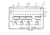
- FIG. 3 is a cross-sectional view schematically showing the configuration of the HEED cold cathode HARP image sensor 10.
- a HEED cold cathode HARP imaging device (hereinafter also referred to as a cold cathode imaging device) 10 includes an active drive type HEED (High-efficiency Electron Emission Device) cold cathode array, HARP (High-gain Avalanche Rushing amorphous Photoconductor) photoelectric conversion film, and the like. It is an image sensor combining the above.
- HEED High-efficiency Electron Emission Device
- HARP High-gain Avalanche Rushing amorphous Photoconductor
- the cold cathode imaging device 10 includes a HARP photoelectric conversion film 11, a HEED cold cathode array chip 24, and a mesh electrode (intermediate electrode) 15 disposed between the HARP photoelectric conversion film 11 and the HEED cold cathode array 20.
- the HEED cold cathode array chip 24 includes an active drive type HEED cold cathode array (hereinafter simply referred to as a HEED cold cathode array) 20, a Y scan driver 22 and an X scan driver 23 (not shown). Are integrally formed.
- a photoelectric conversion film having a HARP structure is used as the photoelectric conversion film and a cold cathode array having a HEED structure is used as the cold cathode array will be described, these are merely examples and photoelectric conversion films having other configurations and A cold cathode array or an electron supply source may be used.
- the HARP photoelectric conversion film 11 is formed on a translucent conductive film 12, and the translucent conductive film 12 is formed on a translucent substrate 13.
- the HARP photoelectric conversion film 11 is mainly composed of amorphous selenium (Se), but other materials such as silicon (Si), lead oxide (PbO), cadmium selenide (CdSe), gallium arsenide.
- a compound semiconductor such as (GaAs) can also be used.
- the translucent conductive film 12 can be formed of a tin oxide (SnO 2 ) film, an ITO (indium tin oxide) film, or the like.
- a predetermined positive voltage (hereinafter also referred to as a HARP potential or a HARP voltage) is applied to the translucent conductive film 12 via a connection terminal (input / output terminal) T1 provided in the glass housing 10A. Is done.
- substrate 13 should just be formed with the material which permeate
- transmits the light of the wavelength which the cold cathode image pick-up element 10 images.
- it is made of a material such as glass that transmits visible light
- it is formed of a material such as sapphire or quartz glass that transmits ultraviolet light.
- it may be formed of a material that transmits X-rays, such as beryllium (Be), silicon (Si), boron nitride (BN), aluminum oxide (Al 2 O 3 ), or the like. That's fine.
- the mesh electrode 15 is provided with a plurality of openings and is formed of a known metal material, alloy, semiconductor material, or the like.
- a predetermined positive voltage (hereinafter also referred to as mesh voltage or mesh potential) is applied to the mesh electrode 15 via the connection terminal T5.
- the mesh electrode is an intermediate electrode provided for electron acceleration and surplus electron recovery.
- the gate electrode of a MOS (Metal Oxide Semiconductor) transistor that drives the HEED is connected to an X scan driver 23 (horizontal scan circuit), and the source electrode (S) is Y scanned. Connected to a driver 22 (vertical scanning circuit), dot sequential scanning is performed.
- the Y scan driver 22 and the X scan driver 23 are configured as one chip integrally with the HEED cold cathode array 20 on the HEED cold cathode array chip 24, and are provided in the glass housing 10A (not shown). Signals, voltages, and the like necessary for driving the HEED cold cathode array chip 24 are supplied through connection terminals (input / output terminals) T2, T3, and T4 provided in the glass housing 10A.
- All these components are vacuum-sealed in a glass housing 10A sealed with frit glass or indium metal.
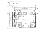
- FIG. 4 is a block diagram showing the configuration of the HEED cold cathode array 20, the Y scan driver 22 that drives the HEED cold cathode array 20, the X scan driver 23, and the controller 25 that controls the entire apparatus.
- the Y scan driver 22 and the X scan driver 23 are configured as one chip as the HEED cold cathode array chip 24.
- the controller 25 and other circuits described later may be provided on the chip.
- the HEED cold cathode array 20 is an active drive field emission array (FEA: Field) in which a HEED cold cathode array is directly laminated and integrated on a drive circuit LSI formed on a Si wafer. It is possible to cope with high-speed driving (for example, the driving pulse width of one pixel is several tens of ns or less) of the imaging operation in which dot sequential scanning is performed.
- the HEED cold cathode array 20 has n rows and m columns connected to scanning drive lines (hereinafter simply referred to as scanning lines) of n lines and m lines in the Y direction (vertical direction) and the X direction (horizontal direction), respectively.
- It is composed of a plurality of pixels in a matrix array (number of pixels is n ⁇ m). For example, it is configured as a high-definition HEED cold cathode array having 640 ⁇ 480 pixels (VGA standard).
- the Y scan driver 22 and the X scan driver 23 perform dot sequential scanning and pixel scanning based on control signals such as a vertical synchronization signal (V-Sync), a horizontal synchronization signal (H-Sync), and a clock signal (CLK) from the controller 25.
- V-Sync vertical synchronization signal
- H-Sync horizontal synchronization signal
- CLK clock signal
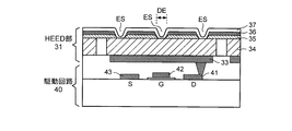
- FIG. 5 is a diagram for explaining the structure of the active drive type HEED cold cathode array 20, and is a partial sectional view schematically showing an enlarged pixel portion.
- a drive circuit 40 composed of a MOS transistor array and a Y scan driver 22 and an X scan driver 23 that drive and control the drive circuit 40 are formed, and then a HEED portion 31 is formed above the drive circuit 40. Has been.
- the HEED portion 31 includes a lower electrode 33, a silicon (Si) layer 34, a silicon oxide (SiO x) layer 35, for example, an upper electrode 36 made of tungsten (W), and a carbon (C) layer 37.
- This is a MIS (Metal-Insulator-Semiconductor) -type cold cathode electron emission source having a structure.
- the upper electrode 36 of the HEED cold cathode array 20 is common to all pixels, and the lower electrode 33 and the Si layer 34 are divided to electrically separate each pixel.
- the lower electrode 33 of the HEED portion 31 is connected to the drain electrode D of the MOS transistor of the drive circuit 40 through a via hole. Further, as described above, the gate electrode G and the source electrode S of the MOS transistor are connected to the X scan driver 23 and the Y scan driver 22. Then, switching of the pixel that emits electrons is performed by controlling the drain potential of the MOS transistor, that is, the potential of the lower electrode 33 of each pixel of the HEED portion 31.
- the number of pixels of the HEED cold cathode array 20 is, for example, 640 ⁇ 480 pixels (VGA), and the size of one pixel is 20 ⁇ 20 ⁇ m 2 .
- An emission site ES that is an opening for electron emission is provided on the surface of one pixel.
- 3 ⁇ 3 emission sites ES (1 ⁇ m ⁇ ) having a diameter DE of about 1 ⁇ m are formed in an 8 ⁇ 8 ⁇ m 2 region of one pixel.
- an electron current of several microamperes ( ⁇ A) is emitted from one emission site ES (emission current density is about 4 A / cm 2 ).
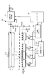
- FIG. 6 is a diagram schematically illustrating the configuration of the imaging apparatus 50 according to the present embodiment.
- the imaging device 50 includes an image signal detection unit 51 and a controller 25 that controls the Y scanning driver 22, the X scanning driver 23, and the image signal detection unit 51.
- an external power supply circuit is connected to the translucent conductive film 12, and a predetermined positive voltage (HARP voltage) Vharp is applied to the HARP photoelectric conversion film 11, and through the capacitor C1.
- the HARP current is configured to be supplied to the image signal detection unit 51.
- Each component of the imaging device 50 including the Y scanning driver 22, the X scanning driver 23, the image signal detection unit 51, and the controller 25 operates (synchronously) based on the clock signal (CLK), and will be described here. Various operations such as detection of various signals, driver driving, and signal processing are performed.
- CLK clock signal
- FIG. 7 is a block diagram showing a configuration of the image signal detection unit 51.
- the image signal detector 51 includes a HARP signal detector 53, an integrator 55, and a sample / hold circuit 56. As described above, these components of the image signal detection unit 51 operate based on the control of the controller 25 and the clock signal (CLK).
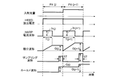
- FIG. 8 schematically shows the output signal waveform of each component of the image signal detection unit 51.
- the pixel period (pixel period) is also referred to as pixel periods PX (j) and PX (j + 1). Note that in an imaging device having 640 ⁇ 480 pixels (VGA standard), the length of a pixel period is generally about several tens ns (nanoseconds), for example, 80 ns.
- the HARP signal detector 53 is connected to the capacitor C1 provided in the HARP photoelectric conversion film 11, and detects the HARP current signal for each pixel based on the clock signal (CLK).
- FIG. 8 shows a case where the amount of emitted electrons from the elements corresponding to the pixels PX (j) and PX (j + 1) of the HEED cold cathode array 20 is equal, and the HARP photoelectric conversion film 11 is applied to the pixel region.
- the case where the incident light amounts are different that is, the case where the incident light amount of PX (j + 1) is larger than the incident light amount of PX (j) is shown.
- the duration of the HARP current neutralization current
- T (j) ⁇ T (j + 1).
- the integrator 55 integrates the HARP current for each of the pixel periods PX (j) and PX (j + 1) while resetting the integration value at the end of the pixel period.
- the integrator 55 can be configured using, for example, an operational amplifier. Alternatively, a circuit using current sinking and capacitor charging can be used.
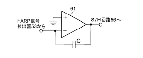
- FIG. 13 is a circuit diagram showing an example of the circuit configuration of the integrator 55. That is, the integrator 55 includes, for example, an operational amplifier 61 and a capacitor C. The non-inverting input (+) of the operational amplifier 61 is grounded (GND), and the inverting input ( ⁇ ) and the output are connected via a capacitor C. The output of the operational amplifier 61 is connected to a sample and hold (S / H) circuit 56. The inverting input ( ⁇ ) of the operational amplifier 61 is connected to the HARP signal detector 53 and supplied with a HARP current signal. Accordingly, the HARP current signal from the HARP signal detector 53 is integrated by the integrator 55, and the integrated value is supplied to the sample and hold circuit 56. Further, a resistor may be provided in series between the input side of the operational amplifier 61, that is, between the inverting input ( ⁇ ) and the HARP signal detector 53.
- the integrator 55 is provided with a reset circuit (not shown) that discharges the electric charge of the capacitor C. As described above, each component of the image signal detection unit 51 including the integrator 55 operates under the control of the controller 25. As described in detail later, the integral value of the integrator 55 is reset by the control of the controller 25 at the end of the pixel period.
- FIG. 14 shows an emitter-sucking type integrator using a bipolar transistor 62 and a capacitor C. That is, the HARP current signal from the HARP signal detector 53 is supplied to the emitter of the bipolar transistor 62. Further, the collector connected to the capacitor C is connected to the sample and hold circuit 56, and the integral value of the HARP current signal is supplied to the sample and hold circuit 56.
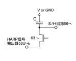
- FIG. 15 shows a source suction type integrator using a field effect transistor (FET) 63 and a capacitor C. That is, the HARP current signal from the HARP signal detector 53 is supplied to the source of the FET 63. The drain connected to the capacitor C is connected to the sample and hold circuit 56, and the integral value of the HARP current signal is supplied to the sample and hold circuit 56.
- FET field effect transistor
- the configuration of the integrator 55 is not limited to these. Any structure that integrates the HARP current signal and outputs the integrated value may be used.
- the integrator 55 resets the integration value at the end of the pixel period.
- the sample and hold circuit 56 samples the integrated waveform of the HARP current in a predetermined sampling period ST at the end of each pixel period, and holds the sampling value.
- the sample and hold circuit 56 may have a peak detection circuit, detect the peak value of the integrated waveform in each pixel period, and hold the peak value. In the following, an example will be described in which the sample and hold circuit 56 samples and holds the integral value at the end of each pixel period.
- the sample and hold circuit 56 outputs the hold value as the image signal SV. Therefore, the image signal detection unit 51 can generate an accurate image signal corresponding to the amount of light incident on each pixel region of the HARP photoelectric conversion film 11.
- FIG. 9 shows the case where the amount of incident light to each pixel region of the HARP photoelectric conversion film 11 is equal and the amount of emitted electrons from the elements of the HEED cold cathode array 20 is different, that is, the amount of HEED emitted electrons (emitted current) E (j). ⁇ E (j + 1) is shown.
- the HARP current value pulse wave height
- Ih (j) ⁇ Ih (j + 1) the HARP current period is T (j)> T (j + 1).
- the integrator 55 integrates the HARP current for each pixel period PX (j), PX (j + 1) +1 while resetting the integration value at the end of each pixel period.
- the image signal detection unit 51 can generate an accurate image signal corresponding to the amount of light incident on the pixel region of the HARP photoelectric conversion film 11. Further, since the integrator 55 is used, noise due to variations in the amount of emitted electrons does not occur.
- the amount of incident light to each pixel region is the same and the amount of emitted electrons is different has been described.
- the amount of incident light to each pixel region is different, and Even when the amount of emitted electrons from the elements of the HEED cold cathode array 20 is different, an accurate integrated value corresponding to the amount of incident light can be obtained, and the noise caused by the variation in the amount of emitted electrons is also the same. .
- the conventional configuration using the LPF for signal detection has a problem that noise due to variations in the amount of emitted electrons of the electron-emitting devices occurs in the image signal.
- the signal-to-noise ratio (S / N) is high and high. An image signal with high image quality can be generated.
- FIG. 10 is a block diagram showing a configuration of an image signal detection unit 51 that is Embodiment 2 of the present invention.
- the image signal detection unit 51 includes a HARP signal detector 53, an integrator 55, a sample / hold circuit 56, and a difference calculator 57.
- FIG. 11 shows each component of the image signal detection unit 51 when the amount of incident light on each pixel region of the HARP photoelectric conversion film 11 is different and the amount of electrons emitted from the elements of the HEED cold cathode array 20 is different.
- the output signal waveform is schematically shown. That is, the amount of HEED emission electrons (emission current) is E (j) ⁇ E (j + 1), and the HARP current value (pulse wave height) is Ih (j) ⁇ Ih (j + 1). It is the same as that of an Example.
- G (j) ⁇ G (j + 1).
- the first embodiment has a configuration in which the integrator 55 integrates the HARP current for each pixel period PX (j), PX (j + 1) while resetting the integration value at the end of each pixel period.
- the integrator 55 continues to integrate the HARP current for a predetermined period. That is, the integrator 55 continues to integrate the HARP current over a predetermined number of pixel periods, and performs an integration signal (integration value) reset operation at the end of the last pixel period for each predetermined number of pixel periods. It can be constituted as follows.
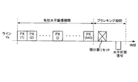
- the integrator 55 continues the integration of the HARP current over the predetermined period over the scanning period of one horizontal scanning line Yk (kth scanning line), and performs a reset operation for each scanning of the horizontal scanning line.
- Yk kth scanning line
- the difference calculator 57 calculates the difference between the integral values of the pixel PX (j ⁇ 1) preceding this from the integral value of the current pixel PX (j), and uses the difference as the current pixel PX.
- (j) be the pixel luminance (pixel value) G (j).
- the reset operation of the integrator 55 is performed in the blanking period after the effective horizontal scanning period which is a period other than the pixel period.
- the reset operation of the integrator 55 may require a time of several ns to several tens of ns due to, for example, extraction of charges in the integrator 55.
- the reset operation is performed in the blanking period without providing the reset period in each pixel period.
- the difference calculator 57 is preceded. What is necessary is just to be comprised so that the difference of a pixel and the present pixel may be calculated.
- the present embodiment since it is not necessary to provide a reset period in each pixel period, it is possible to set the pixel period to be short and to provide an imaging device capable of operating at high speed. it can. Similarly to the above embodiment, no noise is generated in the image signal even if there is a variation in the amount of emitted electrons, and in principle, a signal / noise ratio (S / N) is high and a high-quality image signal is generated. be able to.
- FIG. 16 is a block diagram illustrating a configuration of an integral type detection unit 71 that is Embodiment 3 of the present invention.
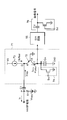
- the integral type detector 71 operates as a HARP signal detector and an integrator. More specifically, integrating detector 71, the current pick-transistor 72, the offset current source 73 consisting of a constant current source, and a storage capacitor C A and the reset circuit 74 operates as a current integrator.
- the output of the integrating detector 71 is supplied to a sample / hold circuit (S / H) 56, and the output of the sample / hold circuit 56 is output as an image signal via a clamp circuit 76.
- the integral type detection unit 71 operates under the control of the controller 25.
- the transistor 72 has a so-called grounded base circuit configuration. Although the case where the base (B) of the transistor 72 is grounded (GND) is shown, it may be fixed to a predetermined base voltage (V B ).
- the base electrode voltage is fixed and the emitter (E) electrode is used as a current injection terminal, and the emitter current injected from the HARP photoelectric conversion film (HARP electrode) 11 through the coupling capacitor C1 is collected in the collector (C )
- the transistor 72 operates as a photoelectric conversion film current detector.
- the base may be used in correspondence with the gate, the emitter in the source, and the collector in correspondence with the drain.
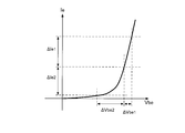
- FIG. 17 is a diagram schematically illustrating the characteristics of the current capturing transistor 72, and is a diagram illustrating the relationship of the emitter current Ie with respect to the base-emitter voltage Vbe.
- the change ( ⁇ Vbe1) of the base-emitter voltage Vbe with respect to the change ( ⁇ Ie1) of the emitter current Ie is small. That is, the impedance is small (the slope of the Ie-Vbe characteristic is large), and the potential fluctuation of the emitter (point Q in FIG. 16) is small.
- the base-emitter voltage Vbe greatly changes ( ⁇ Vbe2) (impedance is large) with respect to the change ( ⁇ Ie2) of the emitter current Ie.
- the emitter electrode is connected to the HARP electrode (HARP photoelectric conversion film) 11 through the coupling capacitor C1
- the fluctuation component of the base-emitter voltage Vbe is also applied to the HARP electrode 11 through capacitive coupling by the coupling capacitor C1.
- This fluctuation is an alternating current component and is pulsed as described above, and therefore disturbs the HARP voltage (Vharp) and at the same time causes noise.
- the HARP voltage Vharp is closely related to the sensitivity of the HARP photoelectric conversion film 11, the disturbance of the voltage applied to the photoelectric conversion film 11 becomes the detection sensitivity.
- the HARP detection current is an AC component detected through capacitive coupling, and current may flow in the negative direction (current In indicated by a broken line arrow in the figure). Therefore, when the current direction changes from minus to plus or vice versa, distortion occurs or detection gain fluctuates.
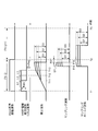
- FIG. 18 is a diagram schematically showing output signal waveforms of each component of the present embodiment.
- an offset current source 73 for superimposing an offset current (Ioffset) on the HARP electrode current is provided. That is, as shown in FIG. 18, the offset current Ioffset is superimposed on the HARP electrode current (detection current) Iharp flowing into the emitter electrode of the transistor 72 via the coupling capacitor C1.
- the transistor 72 operates in an operation range in which the variation of the base-emitter voltage Vbe with respect to the variation of the emitter current is small (impedance is small).
- the potential fluctuation at the emitter electrode Q point, that is, the HARP current detection point
- the potential fluctuation to the HARP voltage Vharp via the coupling capacitor C1 can be suppressed to a small value. Therefore, disturbance of the detection current and sensitivity of the HARP photoelectric conversion film 11 can be suppressed.
- FIG. 18 shows a case where there are three luminances (luminances L1, L2, L3, L1 ⁇ L2 ⁇ L3) in the pixel period PX (j). That is, when the luminance of the pixel period PX (j) is L1, the current integration of the superimposed current (Iharp + Ioffset) is started from the start time (T1) of the pixel period PX (j), and the neutralization of holes is finished.
- the reset circuit 74 includes a switch connected in parallel between both terminals of the storage capacitor C A , and conducts between both terminals of the capacitor C A according to a control signal (reset signal) Srs from the controller 25. Then, the accumulated charge is discharged and a reset operation is performed.
- the reset circuit 74 can be composed of a transistor such as an FET, for example.
- An integral value G1 at the time (T2) is obtained.
- the luminance in the pixel period PX (j) is L2 and L3
- the offset current Ioffset is preferably a value such that the HARP current is always positive according to the amount of electrons emitted from the HEED electron emission source. That is, it is preferably larger than the emission current (absolute value) of HEED. Specifically, the current is preferably larger than the current due to the emitted electrons from one pixel (the total number of emitted electrons from the emission site ES in one pixel).
- the integration output from the integration type detection unit 71 is output as an image signal via the sample and hold (S / H) circuit 56 and the clamp circuit 76.
- the clamp circuit 76 includes, for example, a capacitor Ccl connected in series with the output of the S / H circuit 56, and a transistor such as an FET provided between the image signal output line and the ground potential (GND). It can be configured as a circuit comprising In the reproduction of the AC signal, the DC (direct current) level is not fixed. Therefore, the output terminal (image signal output) from the S / H circuit 56 is clamped to determine the DC level (that is, in the case of an image signal, the black level is fixed to 0V). That is, the clamp circuit 76 performs an operation for eliminating the DC deviation remaining in the output of the integral type detection unit 71.
- the switch of the clamp circuit 76 is turned on, and the image signal output voltage is set to 0 V (ground point). ). That is, clamping is performed so that the voltage at the time of blanking (the luminance value is 0) is forcibly set to 0V. Thereafter, the switch of the clamp circuit 76 is turned off (off).
- an image luminance value (voltage difference) based on blanking (black level, 0 V) is obtained. That is, blanking (black level) is used as a reference for image luminance value (luminance value is zero). That is, it is possible to generate an image signal with an accurate brightness with a black level.
- the clamping operation can be performed by a control signal (clamp signal Scl) from the controller 25, for example.
- a control signal clamp signal Scl
- the above circuit configuration of the clamp circuit 76 is merely an example, and the level of the image luminance value is set to a predetermined DC level (such as 0 V) during the period when the image signal is black level (the luminance value is zero) during blanking or the like. What is necessary is just to be comprised so that it may confirm.
- the offset current is superimposed on the HARP signal current to suppress the voltage fluctuation of the current detection terminal due to the change of the signal current, and the voltage fluctuation to the capacitor-coupled HARP electrode. Can be suppressed. Therefore, it is possible to provide an imaging device that suppresses disturbance in the luminance detection current and sensitivity, generates a high-quality image signal with a high signal-to-noise ratio (S / N).
- the above embodiments can be applied in combination as appropriate.
- the HEED cold cathode array is used as the cold cathode array and the HARP photoelectric conversion film is used as the photoelectric conversion film.
- various cold cathode arrays, electron supply sources, photoelectric conversions are described.
- the present invention can be applied to an imaging device using a film.
- the materials, numerical values, and the like shown in the above embodiments are merely examples.
Landscapes
- Engineering & Computer Science (AREA)
- Multimedia (AREA)
- Signal Processing (AREA)
- Transforming Light Signals Into Electric Signals (AREA)
- Solid State Image Pick-Up Elements (AREA)
Abstract
Description
光電変換膜(HARP)にはアバランシェ増倍のための高電圧が印加されている。HARP電流検出器は、HARP電極と結合キャパシタによって結合され、HARP電流を検出するように構成されている。しかしながら、HARP検出電流によりHARP電流検出器において電位変動が生じ、その電位変動が結合キャパシタによる容量結合を通じてHARP電極に印加されることによって光電変換膜(HARP)への印加電圧を乱れさせてノイズの原因になるという問題があることが分かった。
光電変換膜とキャパシタを介して結合され、光電変換膜に生成された正孔と電子供給源アレイから光電変換膜に供給された電子とが結合することによって流れる光電変換膜電流を検出する光電変換膜電流検出器と、
オフセット電流を生成して光電変換膜電流に重畳するオフセット電流源と、
光電変換膜電流にオフセット電流が重畳された電流を時間積分して積分信号を生成する積分器と、
画素領域の各々に電子を供給する画素期間ごとに上記積分信号をサンプリングして画像信号を生成するサンプリング手段と、を有している。
[撮像装置の構成及び動作]
図6は、本実施例の撮像装置50の構成を模式的に示す図である。撮像装置50には、画像信号検出部51と、Y走査ドライバ22、X走査ドライバ23及び画像信号検出部51を制御するコントローラ25とが設けられている。
Claims (4)
- アバランシェ増倍により光入射に対応した正孔を生成する光電変換膜と、複数の電子供給源がマトリクス状に配置された電子供給源アレイと、前記電子供給源アレイを走査して前記光電変換膜の複数の画素領域に電子を順次供給する走査ドライバと、を備えた撮像装置であって、
前記光電変換膜とキャパシタを介して結合され、前記光電変換膜に生成された正孔と前記電子供給源アレイから前記光電変換膜に供給された電子とが結合することによって流れる光電変換膜電流を検出する光電変換膜電流検出器と、
オフセット電流を生成して前記光電変換膜電流に重畳するオフセット電流源と、
前記光電変換膜電流に前記オフセット電流が重畳された電流を時間積分して積分信号を生成する積分器と、
前記画素領域の各々に電子を供給する画素期間ごとに前記積分信号をサンプリングして画像信号を生成するサンプリング手段と、を有することを特徴とする撮像装置。 - 前記積分信号を前記画素期間ごとにリセットするリセット手段を有することを特徴とする請求項1に記載の撮像装置。
- 前記オフセット電流は、前記電子供給源の電流よりも大であることを特徴とする請求項1又は2に記載の撮像装置。
- 前記電子供給源アレイの走査におけるブランキング期間に前記サンプリング手段のサンプリング出力端子を接地電位にクランプさせるクランプ回路を有することを特徴とする請求項1ないし3のいずれか1に記載の撮像装置。
Priority Applications (2)
| Application Number | Priority Date | Filing Date | Title |
|---|---|---|---|
| US13/143,264 US20110285888A1 (en) | 2009-01-09 | 2009-12-25 | Image sensing device |
| JP2010545724A JPWO2010079702A1 (ja) | 2009-01-09 | 2009-12-25 | 撮像装置 |
Applications Claiming Priority (2)
| Application Number | Priority Date | Filing Date | Title |
|---|---|---|---|
| JPPCT/JP2009/050229 | 2009-01-09 | ||
| PCT/JP2009/050229 WO2010079612A1 (ja) | 2009-01-09 | 2009-01-09 | 撮像装置 |
Publications (1)
| Publication Number | Publication Date |
|---|---|
| WO2010079702A1 true WO2010079702A1 (ja) | 2010-07-15 |
Family
ID=42316390
Family Applications (2)
| Application Number | Title | Priority Date | Filing Date |
|---|---|---|---|
| PCT/JP2009/050229 Ceased WO2010079612A1 (ja) | 2009-01-09 | 2009-01-09 | 撮像装置 |
| PCT/JP2009/071579 Ceased WO2010079702A1 (ja) | 2009-01-09 | 2009-12-25 | 撮像装置 |
Family Applications Before (1)
| Application Number | Title | Priority Date | Filing Date |
|---|---|---|---|
| PCT/JP2009/050229 Ceased WO2010079612A1 (ja) | 2009-01-09 | 2009-01-09 | 撮像装置 |
Country Status (4)
| Country | Link |
|---|---|
| US (1) | US20110285888A1 (ja) |
| JP (1) | JPWO2010079702A1 (ja) |
| TW (1) | TW201119371A (ja) |
| WO (2) | WO2010079612A1 (ja) |
Families Citing this family (2)
| Publication number | Priority date | Publication date | Assignee | Title |
|---|---|---|---|---|
| JPWO2010079613A1 (ja) * | 2009-01-09 | 2012-06-21 | パイオニア株式会社 | 撮像装置 |
| US10827090B1 (en) * | 2019-09-16 | 2020-11-03 | Innolux Corporation | Electronic device and method for operating electronic device |
Citations (7)
| Publication number | Priority date | Publication date | Assignee | Title |
|---|---|---|---|---|
| JPH01288180A (ja) * | 1988-05-16 | 1989-11-20 | Seiko Epson Corp | Mos型イメージセンサー信号処理回路 |
| JPH09154067A (ja) * | 1995-11-30 | 1997-06-10 | Fuji Photo Film Co Ltd | 固体撮像素子の信号読出装置 |
| JP2004072258A (ja) * | 2002-08-02 | 2004-03-04 | Nippon Hoso Kyokai <Nhk> | 固体撮像装置及びその駆動方法 |
| JP2007109742A (ja) * | 2005-10-11 | 2007-04-26 | Rohm Co Ltd | 発光制御装置およびそれを用いた電子機器 |
| JP2008148128A (ja) * | 2006-12-12 | 2008-06-26 | Pioneer Electronic Corp | 撮像装置 |
| JP2008147083A (ja) * | 2006-12-12 | 2008-06-26 | Pioneer Electronic Corp | 撮像装置 |
| JP2008205638A (ja) * | 2007-02-16 | 2008-09-04 | Texas Instr Japan Ltd | 固体撮像装置及びその動作方法 |
-
2009
- 2009-01-09 WO PCT/JP2009/050229 patent/WO2010079612A1/ja not_active Ceased
- 2009-12-25 WO PCT/JP2009/071579 patent/WO2010079702A1/ja not_active Ceased
- 2009-12-25 JP JP2010545724A patent/JPWO2010079702A1/ja not_active Withdrawn
- 2009-12-25 US US13/143,264 patent/US20110285888A1/en not_active Abandoned
-
2010
- 2010-01-08 TW TW099100375A patent/TW201119371A/zh unknown
Patent Citations (7)
| Publication number | Priority date | Publication date | Assignee | Title |
|---|---|---|---|---|
| JPH01288180A (ja) * | 1988-05-16 | 1989-11-20 | Seiko Epson Corp | Mos型イメージセンサー信号処理回路 |
| JPH09154067A (ja) * | 1995-11-30 | 1997-06-10 | Fuji Photo Film Co Ltd | 固体撮像素子の信号読出装置 |
| JP2004072258A (ja) * | 2002-08-02 | 2004-03-04 | Nippon Hoso Kyokai <Nhk> | 固体撮像装置及びその駆動方法 |
| JP2007109742A (ja) * | 2005-10-11 | 2007-04-26 | Rohm Co Ltd | 発光制御装置およびそれを用いた電子機器 |
| JP2008148128A (ja) * | 2006-12-12 | 2008-06-26 | Pioneer Electronic Corp | 撮像装置 |
| JP2008147083A (ja) * | 2006-12-12 | 2008-06-26 | Pioneer Electronic Corp | 撮像装置 |
| JP2008205638A (ja) * | 2007-02-16 | 2008-09-04 | Texas Instr Japan Ltd | 固体撮像装置及びその動作方法 |
Also Published As
| Publication number | Publication date |
|---|---|
| US20110285888A1 (en) | 2011-11-24 |
| JPWO2010079702A1 (ja) | 2012-06-21 |
| WO2010079612A1 (ja) | 2010-07-15 |
| TW201119371A (en) | 2011-06-01 |
Similar Documents
| Publication | Publication Date | Title |
|---|---|---|
| US6627474B2 (en) | Increasing pixel conversion gain in CMOS image sensors | |
| US9490291B2 (en) | Solid state imaging device and camera system | |
| JP3827145B2 (ja) | 固体撮像装置 | |
| CA2639498C (en) | Device and pixel architecture for high resolution digital imaging | |
| US8420994B2 (en) | Detecting device and solid-state imaging device | |
| US10621408B2 (en) | Fingerprint detection circuit, detection method for fingerprint detection circuit, and fingerprint sensor | |
| US11006062B2 (en) | Pixel sensing circuit and driving method thereof, image sensor and electronic device | |
| JP2013046411A (ja) | 感知装置および感知方法 | |
| JP5106284B2 (ja) | 撮像装置 | |
| CN103067666A (zh) | 图像拍摄装置和图像拍摄显示系统 | |
| JP5066392B2 (ja) | 撮像装置 | |
| US20120194881A1 (en) | Image sensing apparatus | |
| WO2010079702A1 (ja) | 撮像装置 | |
| JP5041875B2 (ja) | 撮像装置 | |
| US9641775B2 (en) | Imaging apparatus, imaging system, and driving method of imaging apparatus | |
| CN1910903B (zh) | 图像传感器 | |
| WO2010079613A1 (ja) | 撮像装置 | |
| JP2007508763A (ja) | 感光装置の駆動方法 | |
| CN1736094A (zh) | 图像传感器 | |
| JPH03285451A (ja) | イメージセンサ | |
| US20250203234A1 (en) | Imaging device | |
| JP7319809B2 (ja) | 放射線撮像装置、その制御方法及び放射線撮像システム | |
| JP2010182642A (ja) | 撮像装置 | |
| NL8200669A (nl) | Televisiekamera voorzien van een voorversterker. | |
| JP2000354205A (ja) | 固体撮像装置 |
Legal Events
| Date | Code | Title | Description |
|---|---|---|---|
| 121 | Ep: the epo has been informed by wipo that ep was designated in this application |
Ref document number: 09837587 Country of ref document: EP Kind code of ref document: A1 |
|
| DPE1 | Request for preliminary examination filed after expiration of 19th month from priority date (pct application filed from 20040101) | ||
| ENP | Entry into the national phase |
Ref document number: 2010545724 Country of ref document: JP Kind code of ref document: A |
|
| NENP | Non-entry into the national phase |
Ref country code: DE |
|
| WWE | Wipo information: entry into national phase |
Ref document number: 13143264 Country of ref document: US |
|
| 122 | Ep: pct application non-entry in european phase |
Ref document number: 09837587 Country of ref document: EP Kind code of ref document: A1 |