WO2010074078A1 - 磁気記憶媒体製造方法、磁気記憶媒体、および情報記憶装置 - Google Patents
磁気記憶媒体製造方法、磁気記憶媒体、および情報記憶装置 Download PDFInfo
- Publication number
- WO2010074078A1 WO2010074078A1 PCT/JP2009/071324 JP2009071324W WO2010074078A1 WO 2010074078 A1 WO2010074078 A1 WO 2010074078A1 JP 2009071324 W JP2009071324 W JP 2009071324W WO 2010074078 A1 WO2010074078 A1 WO 2010074078A1
- Authority
- WO
- WIPO (PCT)
- Prior art keywords
- magnetic
- storage medium
- film
- ion implantation
- manufacturing
- Prior art date
- Legal status (The legal status is an assumption and is not a legal conclusion. Google has not performed a legal analysis and makes no representation as to the accuracy of the status listed.)
- Ceased
Links
Images






Classifications
-
- G—PHYSICS
- G11—INFORMATION STORAGE
- G11B—INFORMATION STORAGE BASED ON RELATIVE MOVEMENT BETWEEN RECORD CARRIER AND TRANSDUCER
- G11B5/00—Recording by magnetisation or demagnetisation of a record carrier; Reproducing by magnetic means; Record carriers therefor
- G11B5/84—Processes or apparatus specially adapted for manufacturing record carriers
- G11B5/855—Coating only part of a support with a magnetic layer
-
- G—PHYSICS
- G11—INFORMATION STORAGE
- G11B—INFORMATION STORAGE BASED ON RELATIVE MOVEMENT BETWEEN RECORD CARRIER AND TRANSDUCER
- G11B5/00—Recording by magnetisation or demagnetisation of a record carrier; Reproducing by magnetic means; Record carriers therefor
- G11B5/62—Record carriers characterised by the selection of the material
- G11B5/64—Record carriers characterised by the selection of the material comprising only the magnetic material without bonding agent
- G11B5/65—Record carriers characterised by the selection of the material comprising only the magnetic material without bonding agent characterised by its composition
-
- Y—GENERAL TAGGING OF NEW TECHNOLOGICAL DEVELOPMENTS; GENERAL TAGGING OF CROSS-SECTIONAL TECHNOLOGIES SPANNING OVER SEVERAL SECTIONS OF THE IPC; TECHNICAL SUBJECTS COVERED BY FORMER USPC CROSS-REFERENCE ART COLLECTIONS [XRACs] AND DIGESTS
- Y10—TECHNICAL SUBJECTS COVERED BY FORMER USPC
- Y10S—TECHNICAL SUBJECTS COVERED BY FORMER USPC CROSS-REFERENCE ART COLLECTIONS [XRACs] AND DIGESTS
- Y10S428/00—Stock material or miscellaneous articles
- Y10S428/90—Magnetic feature
Definitions
- Discrete track type magnetic storage media have been proposed as a magnetic storage medium that achieves a short bit length and high track density by avoiding these magnetic interference and thermal fluctuation phenomena.
- a bit patterned type magnetic storage medium has also been proposed (see, for example, Patent Document 1).
- the position of a recording bit is determined in advance, and a dot (magnetic dot) of a magnetic material is formed at the position of the determined recording bit so that there is no gap between the magnetic dots. Consists of magnetic material.
- the basic form of the magnetic storage medium that achieves the above object includes a substrate, a magnetic part, and a low magnetic part.
- a disk-shaped magnetic disk 10 is housed in a plurality of housings H so as to overlap in the depth direction of the figure.
- This magnetic disk 10 corresponds to a specific embodiment of the magnetic storage medium whose basic form has been described above.
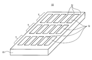
- FIG. 2 is a perspective view schematically showing the structure of the magnetic disk shown in FIG.
- a method for manufacturing the magnetic disk 10 will be described below.
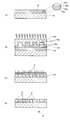
- a resist 3 made of an ultraviolet curable resin is applied on the magnetic film 2, and a mold 4 having nano-sized holes 4 a is placed on the resist 3.
- the resist 3 enters the nano-sized hole 4a, and the dots 3a of the resist 3 are formed.
- the resist 3 is irradiated with ultraviolet rays through the mold 4, so that the resist 3 is cured and the dots 3 a are printed on the magnetic film 2. Further, after the resist 3 is cured, the mold 4 is removed.
- a resist 63 made of an ultraviolet curable resin is applied on the magnetic film 62, and the resist 63 is formed by placing a mold 64 with nano-sized holes 64a on the resist 63.
- the nano-sized holes 64 a enter the dots 63 a of the resist 63.
- the resist 63 is cured by irradiating the resist 63 with ultraviolet rays through the mold 64, and the dots 63 a are printed on the magnetic film 62. After the resist 63 is cured, the mold 64 is removed.
- the process proceeds to the ion implantation process (C), and ions are irradiated from the upper part of the magnetic film 62 on which the dots 63a are printed.
- this ion implantation step (C) mixed ions of N 2 + ions and N + ions are irradiated as in the ion implantation in the above-described experiment.
- the N 2 + ions are divided into two N + ions when they collide with the surface of the magnetic film 62.
- N + ions are implanted into the magnetic film 62. And the saturation magnetization in the injection
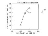
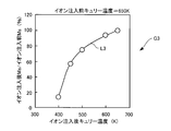
- oxygen ions and nitrogen ions can effectively reduce the saturation magnetization of the magnetic film having the above artificial lattice structure or the magnetic film made of a Co—Cr—Pt base alloy. discovered.
- This application form is based on this discovery and can be said to be suitable.
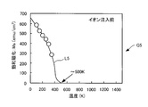
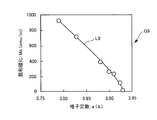
- the magnetic disk manufacturing method of the present embodiment by forming the magnetic film so that the Curie temperature is 600 K or less, the effect of sufficiently reducing the saturation magnetization by ion implantation can be obtained. it can. As a result, according to the magnetic disk manufacturing method of this embodiment, a magnetic disk of a type such as a bit patterned type can be manufactured easily and practically.
Landscapes
- Magnetic Record Carriers (AREA)
- Manufacturing Of Magnetic Record Carriers (AREA)
Abstract
Description
10 磁気ディスク
61 ガラス基板
62 磁性膜
62a Coの原子層
62b Pdの原子層
Claims (11)
- 基板上に、キュリー温度が600K以下となるように磁性膜を形成する磁性膜形成過程と、
前記磁性膜に対し、所定の保護領域を除いた他の領域に対して局所的にイオンを注入するイオン注入過程とを有することを特徴とする磁気記憶媒体製造方法。 - 前記磁性膜形成過程が、前記磁性膜を、該磁性膜のキュリー温度が600K以下となる膜厚で形成する過程であることを特徴とする請求項1記載の磁気記憶媒体製造方法。
- 前記イオン注入過程が、前記保護領域として、前記磁性膜が広がる方向に規則的に配列した複数箇所を用いて、該複数箇所の相互間に対して局所的にイオンを注入する過程であることを特徴とする請求項1又は2記載の磁気記憶媒体製造方法。
- 前記イオン注入過程が、前記イオンとして、酸素イオン及び窒素イオンのうちいずれか一方のイオンを用いる過程であることを特徴とする請求項1から3のうちいずれか1項記載の磁気記憶媒体製造方法。
- 前記磁性膜上に、前記保護領域へのイオンの注入を阻害するマスクを形成するマスク形成過程を有し、
前記イオン注入過程が、前記マスクが形成された磁性膜の上からイオンを当てることで、該マスクで保護された保護領域を除いた他の領域に対して局所的に該イオンを注入する過程であることを特徴とする請求項1から4のうちいずれか1項記載の磁気記憶媒体製造方法。 - 前記マスク形成過程が、前記マスクをレジストで形成する過程であることを特徴とする請求項5記載の磁気記憶媒体製造方法。
- 前記マスク形成過程が、前記マスクをレジストで、ナノインプリントプロセスによって形成する過程であることを特徴とする請求項5又は6記載の磁気記憶媒体製造方法。
- 基板と、
前記基板上に、キュリー温度が600K以下となるように形成された磁性膜を有し情報が磁気的に記録される磁性部と、
前記磁性部の磁性膜と連続した磁性膜にイオンが注入されてなる被注入膜を有し該磁性部の飽和磁化よりも小さい飽和磁化を有する低磁性部とを備えたことを特徴とする磁気記憶媒体。 - 前記磁性部が、前記基板上に規則的に複数配列された、各々に情報が磁気的に記録される磁性ドットであり、
前記低磁性部が、前記磁性ドットの相互間に設けられた、該磁性ドット相互の磁気的結合を阻害するドット間分断帯であることを特徴とする請求項8記載の磁気記憶媒体。 - 基板と、該基板上に、キュリー温度が600K以下となるように形成された磁性膜を有し情報が磁気的に記録される磁性部と、該磁性部の磁性膜と連続した磁性膜にイオンが注入されてなる被注入膜を有し該磁性部の飽和磁化よりも小さい飽和磁化を有する低磁性部とを備えた磁気記憶媒体と、
前記磁気記憶媒体に近接あるいは接触して磁性部に磁気的に情報の記録及び/又は再生を行う磁気ヘッドと、
前記磁気ヘッドを前記磁気記憶媒体表面に対して相対的に移動させて、該磁気ヘッドによる情報の記録及び/又は再生となる磁性部上に該磁気ヘッドを位置決めするヘッド位置制御機構とを備えたことを特徴とする情報記憶装置。 - 前記磁気記憶媒体の磁性部が、前記基板上に規則的に複数配列された、各々に情報が磁気的に記録される磁性ドットであり、
前記低磁性部が、前記磁性ドットの相互間に設けられた、該磁性ドット相互の磁気的結合を阻害するドット間分断帯であることを特徴とする請求項10記載の情報記憶装置。
Priority Applications (2)
| Application Number | Priority Date | Filing Date | Title |
|---|---|---|---|
| CN2009801473508A CN102224544A (zh) | 2008-12-26 | 2009-12-22 | 磁存储介质制造方法、磁存储介质以及信息存储装置 |
| US13/131,803 US20110242700A1 (en) | 2008-12-26 | 2009-12-22 | Method of producing magnetic storage medium, magnetic storage medium and information storage device |
Applications Claiming Priority (2)
| Application Number | Priority Date | Filing Date | Title |
|---|---|---|---|
| JP2008332333A JP5394729B2 (ja) | 2008-12-26 | 2008-12-26 | 磁気記憶媒体製造方法、磁気記憶媒体、および情報記憶装置 |
| JP2008-332333 | 2008-12-26 |
Publications (1)
| Publication Number | Publication Date |
|---|---|
| WO2010074078A1 true WO2010074078A1 (ja) | 2010-07-01 |
Family
ID=42287687
Family Applications (1)
| Application Number | Title | Priority Date | Filing Date |
|---|---|---|---|
| PCT/JP2009/071324 Ceased WO2010074078A1 (ja) | 2008-12-26 | 2009-12-22 | 磁気記憶媒体製造方法、磁気記憶媒体、および情報記憶装置 |
Country Status (5)
| Country | Link |
|---|---|
| US (1) | US20110242700A1 (ja) |
| JP (1) | JP5394729B2 (ja) |
| KR (1) | KR20110106277A (ja) |
| CN (1) | CN102224544A (ja) |
| WO (1) | WO2010074078A1 (ja) |
Cited By (1)
| Publication number | Priority date | Publication date | Assignee | Title |
|---|---|---|---|---|
| US20120196155A1 (en) * | 2010-07-28 | 2012-08-02 | Applied Materials, Inc. | Resist fortification for magnetic media patterning |
Families Citing this family (2)
| Publication number | Priority date | Publication date | Assignee | Title |
|---|---|---|---|---|
| KR101294392B1 (ko) * | 2008-09-19 | 2013-08-08 | 가부시키가이샤 알박 | 자기 기록 매체의 제조 방법 |
| JP5485588B2 (ja) * | 2009-05-26 | 2014-05-07 | エイチジーエスティーネザーランドビーブイ | 磁気記録媒体及びその製造方法 |
Citations (3)
| Publication number | Priority date | Publication date | Assignee | Title |
|---|---|---|---|---|
| JPH05205257A (ja) * | 1992-01-28 | 1993-08-13 | Toshiba Corp | 磁気記録媒体 |
| JPH11213375A (ja) * | 1998-01-29 | 1999-08-06 | Canon Inc | 磁気記録媒体およびその製造方法 |
| JP2002501300A (ja) * | 1998-01-12 | 2002-01-15 | サントル、ナショナール、ド、ラ、ルシェルシュ、シアンティフィク、(セーエヌエルエス) | 特に磁気記録または光磁気記録用の磁気彫刻法 |
Family Cites Families (5)
| Publication number | Priority date | Publication date | Assignee | Title |
|---|---|---|---|---|
| US6838227B2 (en) * | 2001-11-30 | 2005-01-04 | Seagate Technology Llc | Polystyrene as a resist for making patterned media |
| JP2008029573A (ja) * | 2006-07-28 | 2008-02-14 | Kao Corp | 美容方法 |
| JP2008084432A (ja) * | 2006-09-27 | 2008-04-10 | Hoya Corp | 磁気記録媒体、及び磁気記録媒体の製造方法 |
| JP2008135092A (ja) * | 2006-11-27 | 2008-06-12 | Showa Denko Kk | 磁気記録媒体の製造方法、及び磁気記録再生装置 |
| JP4703604B2 (ja) * | 2007-05-23 | 2011-06-15 | 株式会社東芝 | 磁気記録媒体およびその製造方法 |
-
2008
- 2008-12-26 JP JP2008332333A patent/JP5394729B2/ja active Active
-
2009
- 2009-12-22 CN CN2009801473508A patent/CN102224544A/zh active Pending
- 2009-12-22 US US13/131,803 patent/US20110242700A1/en not_active Abandoned
- 2009-12-22 WO PCT/JP2009/071324 patent/WO2010074078A1/ja not_active Ceased
- 2009-12-22 KR KR1020117010718A patent/KR20110106277A/ko not_active Ceased
Patent Citations (3)
| Publication number | Priority date | Publication date | Assignee | Title |
|---|---|---|---|---|
| JPH05205257A (ja) * | 1992-01-28 | 1993-08-13 | Toshiba Corp | 磁気記録媒体 |
| JP2002501300A (ja) * | 1998-01-12 | 2002-01-15 | サントル、ナショナール、ド、ラ、ルシェルシュ、シアンティフィク、(セーエヌエルエス) | 特に磁気記録または光磁気記録用の磁気彫刻法 |
| JPH11213375A (ja) * | 1998-01-29 | 1999-08-06 | Canon Inc | 磁気記録媒体およびその製造方法 |
Cited By (3)
| Publication number | Priority date | Publication date | Assignee | Title |
|---|---|---|---|---|
| US20120196155A1 (en) * | 2010-07-28 | 2012-08-02 | Applied Materials, Inc. | Resist fortification for magnetic media patterning |
| US8658242B2 (en) * | 2010-07-28 | 2014-02-25 | Applied Materials, Inc. | Resist fortification for magnetic media patterning |
| US9646642B2 (en) | 2010-07-28 | 2017-05-09 | Applied Materials, Inc. | Resist fortification for magnetic media patterning |
Also Published As
| Publication number | Publication date |
|---|---|
| JP2010153003A (ja) | 2010-07-08 |
| US20110242700A1 (en) | 2011-10-06 |
| KR20110106277A (ko) | 2011-09-28 |
| CN102224544A (zh) | 2011-10-19 |
| JP5394729B2 (ja) | 2014-01-22 |
Similar Documents
| Publication | Publication Date | Title |
|---|---|---|
| JP5916985B2 (ja) | 熱アシスト記録用磁気ディスクへの磁気記録方法 | |
| CN101542604A (zh) | 制造磁记录介质的方法以及磁记录和再现装置 | |
| JP2008052860A (ja) | 磁気記録媒体の製造方法、及び磁気記録再生装置 | |
| JP5422912B2 (ja) | 磁気記録媒体及びその製造方法及び磁気記録再生装置 | |
| WO2010058793A1 (ja) | 磁気記憶媒体製造方法、磁気記憶媒体、および情報記憶装置 | |
| JP5394729B2 (ja) | 磁気記憶媒体製造方法、磁気記憶媒体、および情報記憶装置 | |
| JP2005223177A (ja) | 磁性膜の形成方法、磁性パターンの形成方法及び磁気記録媒体の製造方法 | |
| JP5415745B2 (ja) | 磁気記憶媒体製造方法、磁気記憶媒体、および情報記憶装置 | |
| JP4319060B2 (ja) | 磁性膜の形成方法、磁性パターンの形成方法及び磁気記録媒体の製造方法 | |
| JP4319059B2 (ja) | 磁性膜の形成方法、磁性パターンの形成方法及び磁気記録媒体の製造方法 | |
| JP2011138586A (ja) | 磁気記録媒体及びその製造方法 | |
| JP2009238273A (ja) | 磁気記録媒体の製造方法及び磁気記録媒体及び磁気記録再生装置 | |
| KR101570893B1 (ko) | 자기 기록 매체 제조 방법, 자기 기록 매체, 및 정보 기억 장치 | |
| JP5398228B2 (ja) | 膜製造方法 | |
| WO2010058792A1 (ja) | 磁気記憶媒体製造方法、磁気記憶媒体、および情報記憶装置 | |
| JP5394688B2 (ja) | 磁気記憶媒体製造方法、磁気記憶媒体、および情報記憶装置 | |
| JP2010134975A (ja) | 磁気記憶媒体製造方法、磁気記憶媒体、および情報記憶装置 | |
| JP5329212B2 (ja) | 磁気記憶媒体製造方法 | |
| JP6374421B2 (ja) | 熱アシスト記録用磁気ディスクおよび熱アシスト記録用磁気ディスクの製造方法 | |
| JP2005223178A (ja) | 磁性膜の形成方法、磁性パターンの形成方法及び磁気記録媒体の製造方法 | |
| JP5345562B2 (ja) | 磁気記録媒体の製造方法 | |
| JP2010146604A (ja) | 磁気記録媒体および磁気記録再生装置 |
Legal Events
| Date | Code | Title | Description |
|---|---|---|---|
| WWE | Wipo information: entry into national phase |
Ref document number: 200980147350.8 Country of ref document: CN |
|
| 121 | Ep: the epo has been informed by wipo that ep was designated in this application |
Ref document number: 09834879 Country of ref document: EP Kind code of ref document: A1 |
|
| ENP | Entry into the national phase |
Ref document number: 20117010718 Country of ref document: KR Kind code of ref document: A |
|
| WWE | Wipo information: entry into national phase |
Ref document number: 13131803 Country of ref document: US |
|
| NENP | Non-entry into the national phase |
Ref country code: DE |
|
| 122 | Ep: pct application non-entry in european phase |
Ref document number: 09834879 Country of ref document: EP Kind code of ref document: A1 |