WO2010073792A1 - 液晶表示装置及びテレビ受信装置 - Google Patents
液晶表示装置及びテレビ受信装置 Download PDFInfo
- Publication number
- WO2010073792A1 WO2010073792A1 PCT/JP2009/067327 JP2009067327W WO2010073792A1 WO 2010073792 A1 WO2010073792 A1 WO 2010073792A1 JP 2009067327 W JP2009067327 W JP 2009067327W WO 2010073792 A1 WO2010073792 A1 WO 2010073792A1
- Authority
- WO
- WIPO (PCT)
- Prior art keywords
- liquid crystal
- backlight
- crystal display
- display device
- signal
- Prior art date
- Legal status (The legal status is an assumption and is not a legal conclusion. Google has not performed a legal analysis and makes no representation as to the accuracy of the status listed.)
- Ceased
Links
Images



Classifications
-
- G—PHYSICS
- G02—OPTICS
- G02F—OPTICAL DEVICES OR ARRANGEMENTS FOR THE CONTROL OF LIGHT BY MODIFICATION OF THE OPTICAL PROPERTIES OF THE MEDIA OF THE ELEMENTS INVOLVED THEREIN; NON-LINEAR OPTICS; FREQUENCY-CHANGING OF LIGHT; OPTICAL LOGIC ELEMENTS; OPTICAL ANALOGUE/DIGITAL CONVERTERS
- G02F1/00—Devices or arrangements for the control of the intensity, colour, phase, polarisation or direction of light arriving from an independent light source, e.g. switching, gating or modulating; Non-linear optics
- G02F1/01—Devices or arrangements for the control of the intensity, colour, phase, polarisation or direction of light arriving from an independent light source, e.g. switching, gating or modulating; Non-linear optics for the control of the intensity, phase, polarisation or colour
- G02F1/13—Devices or arrangements for the control of the intensity, colour, phase, polarisation or direction of light arriving from an independent light source, e.g. switching, gating or modulating; Non-linear optics for the control of the intensity, phase, polarisation or colour based on liquid crystals, e.g. single liquid crystal display cells
- G02F1/133—Constructional arrangements; Operation of liquid crystal cells; Circuit arrangements
- G02F1/1333—Constructional arrangements; Manufacturing methods
- G02F1/1335—Structural association of cells with optical devices, e.g. polarisers or reflectors
- G02F1/1336—Illuminating devices
- G02F1/133602—Direct backlight
- G02F1/133604—Direct backlight with lamps
-
- G—PHYSICS
- G09—EDUCATION; CRYPTOGRAPHY; DISPLAY; ADVERTISING; SEALS
- G09G—ARRANGEMENTS OR CIRCUITS FOR CONTROL OF INDICATING DEVICES USING STATIC MEANS TO PRESENT VARIABLE INFORMATION
- G09G3/00—Control arrangements or circuits, of interest only in connection with visual indicators other than cathode-ray tubes
- G09G3/20—Control arrangements or circuits, of interest only in connection with visual indicators other than cathode-ray tubes for presentation of an assembly of a number of characters, e.g. a page, by composing the assembly by combination of individual elements arranged in a matrix no fixed position being assigned to or needed to be assigned to the individual characters or partial characters
- G09G3/34—Control arrangements or circuits, of interest only in connection with visual indicators other than cathode-ray tubes for presentation of an assembly of a number of characters, e.g. a page, by composing the assembly by combination of individual elements arranged in a matrix no fixed position being assigned to or needed to be assigned to the individual characters or partial characters by control of light from an independent source
- G09G3/3406—Control of illumination source
-
- G—PHYSICS
- G09—EDUCATION; CRYPTOGRAPHY; DISPLAY; ADVERTISING; SEALS
- G09G—ARRANGEMENTS OR CIRCUITS FOR CONTROL OF INDICATING DEVICES USING STATIC MEANS TO PRESENT VARIABLE INFORMATION
- G09G3/00—Control arrangements or circuits, of interest only in connection with visual indicators other than cathode-ray tubes
- G09G3/20—Control arrangements or circuits, of interest only in connection with visual indicators other than cathode-ray tubes for presentation of an assembly of a number of characters, e.g. a page, by composing the assembly by combination of individual elements arranged in a matrix no fixed position being assigned to or needed to be assigned to the individual characters or partial characters
- G09G3/34—Control arrangements or circuits, of interest only in connection with visual indicators other than cathode-ray tubes for presentation of an assembly of a number of characters, e.g. a page, by composing the assembly by combination of individual elements arranged in a matrix no fixed position being assigned to or needed to be assigned to the individual characters or partial characters by control of light from an independent source
- G09G3/36—Control arrangements or circuits, of interest only in connection with visual indicators other than cathode-ray tubes for presentation of an assembly of a number of characters, e.g. a page, by composing the assembly by combination of individual elements arranged in a matrix no fixed position being assigned to or needed to be assigned to the individual characters or partial characters by control of light from an independent source using liquid crystals
- G09G3/3611—Control of matrices with row and column drivers
-
- G—PHYSICS
- G02—OPTICS
- G02F—OPTICAL DEVICES OR ARRANGEMENTS FOR THE CONTROL OF LIGHT BY MODIFICATION OF THE OPTICAL PROPERTIES OF THE MEDIA OF THE ELEMENTS INVOLVED THEREIN; NON-LINEAR OPTICS; FREQUENCY-CHANGING OF LIGHT; OPTICAL LOGIC ELEMENTS; OPTICAL ANALOGUE/DIGITAL CONVERTERS
- G02F1/00—Devices or arrangements for the control of the intensity, colour, phase, polarisation or direction of light arriving from an independent light source, e.g. switching, gating or modulating; Non-linear optics
- G02F1/01—Devices or arrangements for the control of the intensity, colour, phase, polarisation or direction of light arriving from an independent light source, e.g. switching, gating or modulating; Non-linear optics for the control of the intensity, phase, polarisation or colour
- G02F1/13—Devices or arrangements for the control of the intensity, colour, phase, polarisation or direction of light arriving from an independent light source, e.g. switching, gating or modulating; Non-linear optics for the control of the intensity, phase, polarisation or colour based on liquid crystals, e.g. single liquid crystal display cells
- G02F1/133—Constructional arrangements; Operation of liquid crystal cells; Circuit arrangements
- G02F1/1333—Constructional arrangements; Manufacturing methods
- G02F1/1335—Structural association of cells with optical devices, e.g. polarisers or reflectors
- G02F1/1336—Illuminating devices
- G02F1/133601—Illuminating devices for spatial active dimming
-
- G—PHYSICS
- G09—EDUCATION; CRYPTOGRAPHY; DISPLAY; ADVERTISING; SEALS
- G09G—ARRANGEMENTS OR CIRCUITS FOR CONTROL OF INDICATING DEVICES USING STATIC MEANS TO PRESENT VARIABLE INFORMATION
- G09G2320/00—Control of display operating conditions
- G09G2320/02—Improving the quality of display appearance
- G09G2320/0247—Flicker reduction other than flicker reduction circuits used for single beam cathode-ray tubes
-
- G—PHYSICS
- G09—EDUCATION; CRYPTOGRAPHY; DISPLAY; ADVERTISING; SEALS
- G09G—ARRANGEMENTS OR CIRCUITS FOR CONTROL OF INDICATING DEVICES USING STATIC MEANS TO PRESENT VARIABLE INFORMATION
- G09G2320/00—Control of display operating conditions
- G09G2320/06—Adjustment of display parameters
- G09G2320/0626—Adjustment of display parameters for control of overall brightness
- G09G2320/0633—Adjustment of display parameters for control of overall brightness by amplitude modulation of the brightness of the illumination source
-
- G—PHYSICS
- G09—EDUCATION; CRYPTOGRAPHY; DISPLAY; ADVERTISING; SEALS
- G09G—ARRANGEMENTS OR CIRCUITS FOR CONTROL OF INDICATING DEVICES USING STATIC MEANS TO PRESENT VARIABLE INFORMATION
- G09G2320/00—Control of display operating conditions
- G09G2320/06—Adjustment of display parameters
- G09G2320/0626—Adjustment of display parameters for control of overall brightness
- G09G2320/064—Adjustment of display parameters for control of overall brightness by time modulation of the brightness of the illumination source
-
- G—PHYSICS
- G09—EDUCATION; CRYPTOGRAPHY; DISPLAY; ADVERTISING; SEALS
- G09G—ARRANGEMENTS OR CIRCUITS FOR CONTROL OF INDICATING DEVICES USING STATIC MEANS TO PRESENT VARIABLE INFORMATION
- G09G2320/00—Control of display operating conditions
- G09G2320/06—Adjustment of display parameters
- G09G2320/0626—Adjustment of display parameters for control of overall brightness
- G09G2320/0653—Controlling or limiting the speed of brightness adjustment of the illumination source
-
- G—PHYSICS
- G09—EDUCATION; CRYPTOGRAPHY; DISPLAY; ADVERTISING; SEALS
- G09G—ARRANGEMENTS OR CIRCUITS FOR CONTROL OF INDICATING DEVICES USING STATIC MEANS TO PRESENT VARIABLE INFORMATION
- G09G2330/00—Aspects of power supply; Aspects of display protection and defect management
- G09G2330/02—Details of power systems and of start or stop of display operation
- G09G2330/021—Power management, e.g. power saving
-
- G—PHYSICS
- G09—EDUCATION; CRYPTOGRAPHY; DISPLAY; ADVERTISING; SEALS
- G09G—ARRANGEMENTS OR CIRCUITS FOR CONTROL OF INDICATING DEVICES USING STATIC MEANS TO PRESENT VARIABLE INFORMATION
- G09G2360/00—Aspects of the architecture of display systems
- G09G2360/16—Calculation or use of calculated indices related to luminance levels in display data
Definitions
- the present invention relates to a liquid crystal display device and a television receiver including the liquid crystal display device, and more particularly to power saving of a backlight of the liquid crystal display device.
- a backlight using a discharge tube such as a CCFL (Cold Cathode Fluorescent Tube) is known as a backlight of a liquid crystal display device such as a liquid crystal television, and recently, a backlight using a number of LEDs (Light Emitting Diode) is also known. It has been.
- the power consumption of the liquid crystal display device is higher by the backlight than the liquid crystal panel. Therefore, it is necessary to reduce the power consumption of the backlight in order to suppress an increase in power consumption accompanying an increase in the size of the liquid crystal display device.
- Patent Document 1 As a technique for reducing the power consumption of the backlight, for example, in Patent Document 1, when there is no video signal to be displayed on the liquid crystal panel in the standby mode or the like, an auxiliary screen is displayed on the liquid crystal panel. A technique for turning off an LED corresponding to a black display portion is disclosed. JP 2007-086380 A
- the present invention has been completed based on the above-described circumstances, and a liquid crystal display device and a liquid crystal display device that can easily reduce the power consumption of a backlight corresponding to the entire liquid crystal panel.
- An object of the present invention is to provide a television receiving device provided.
- a liquid crystal display device includes a liquid crystal panel that displays an image, a backlight that illuminates the liquid crystal panel from the back, and a backlight control unit that controls the light emission luminance of the backlight. And a video signal processing unit that controls the liquid crystal panel and the backlight based on a video signal and detects that the image is a black display image based on the video signal. And the backlight control unit generates a dimming signal for gradually reducing the light emission luminance until it becomes almost zero in response to detection of the black display image, and supplies the dimming signal to the backlight. .
- the liquid crystal panel displays a black display image
- the light emission luminance of the backlight is gradually reduced until it becomes almost zero. Therefore, the power saving of the backlight corresponding to the entire liquid crystal panel can be easily performed by simply detecting that the image is a black display image. In that case, since the light emission luminance is gradually reduced, it is possible to suppress a sense of incongruity due to the backlight turning off.
- the term “substantially zero” includes the meaning of “zero”.
- the backlight control unit may generate the dimming signal in units of a predetermined period. According to such a configuration, the light emission luminance can be gradually reduced in units of a predetermined period by changing the dimming signal in units of a predetermined period.
- the predetermined period may be one frame period. According to this configuration, the light emission luminance can be reduced corresponding to one frame period. At this time, the dimming signal can be changed in synchronization with the frame signal (vertical synchronization signal).
- the backlight includes a fluorescent tube as a light source
- the dimming signal is a burst signal that alternately switches between a lighting state and a non-lighting state of the fluorescent tube
- the backlight control unit includes the black display image
- the amplitude and / or duty ratio of the burst signal may be gradually decreased in response to the detection of. According to such a structure, when a backlight is comprised with a fluorescent tube, the brightness
- the backlight includes a light emitting diode as a light source, and the backlight control unit gradually decreases the light emission luminance of the light emitting diode in response to detection of the black display image. According to such a configuration, even when the backlight is composed of light emitting diodes, the power consumption of the backlight corresponding to the entire liquid crystal panel can be reduced, and the uncomfortable feeling caused by turning off the backlight is suppressed. can do.
- the backlight control unit may reduce the light emission luminance of the light emitting diode to zero. According to this configuration, the power consumption of the backlight can be reduced to the minimum value.
- the television receiver of the present invention includes the liquid crystal display device. According to this configuration, with the power saving of the liquid crystal display device, the power of the television receiver is also saved.
- the liquid crystal display device which enables the power saving of the backlight corresponding to the whole liquid crystal panel, and the television receiver provided with the said liquid crystal display device can be provided.
- FIG. 1 is a block diagram schematically showing an electrical configuration of a television receiver according to an embodiment of the present invention.
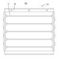
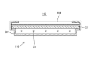
- Schematic plan view showing a configuration example of a backlight of a liquid crystal display device Schematic cross-sectional view showing a configuration example of a liquid crystal display device Time chart schematically showing the time transition of each signal related to backlight power saving control
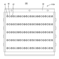
- Schematic plan view showing another configuration example of the backlight Schematic cross-sectional view showing another configuration example of a liquid crystal display device
- a television receiver including the liquid crystal display device according to the present invention is illustrated.
- the present invention is not limited to this, and the liquid crystal display device according to the present invention can be applied to any device that requires image display, such as a personal computer, a game machine, and a measuring instrument.
- FIG. 1 is a schematic block diagram showing a configuration of a television reception device 200 including a liquid crystal display device 100 according to the present invention.
- the tuner 112 selects a channel from the television broadcast signal received by the antenna 111.
- the video input terminal 113 inputs a video signal from an AV device built in the television receiver 200 or externally connected.
- the switching unit 114 switches and outputs the television broadcast signal selected by the tuner 112 and the video signal input via the video input terminal 113.
- the video signal Si switched and output from the switching unit 114 is subjected to video processing in the video signal processing unit 102 of the liquid crystal display device 100.
- the audio signal output from the switching unit 114 is processed by the audio processing unit 115 and output from the speaker 116 as audio.
- the remote control light receiving unit 117 receives a remote control operation signal by infrared rays transmitted from the remote control device 120, and sends it to the control unit 118.
- the control unit 118 detects and analyzes the remote control operation signal received by the remote control light receiving unit 117, and performs operations on the tuner 112, the switching unit 114, the video signal processing unit 102, the LCD control unit 103, the audio processing unit 115, and the like.
- a control signal for controlling is output.
- the liquid crystal display device 100 includes a video signal processing unit 102, an LCD (liquid crystal display device) control unit 103, a liquid crystal panel 104, a backlight control unit 107, and a backlight 110.
- a video signal processing unit 102 an LCD (liquid crystal display device) control unit 103
- a liquid crystal panel 104 a liquid crystal panel 104
- a backlight control unit 107 a backlight 110.
- the video signal processing unit 102 processes the video signal Si input to the liquid crystal display device 100 or the video signal Si read from a recording medium of a recording / reproducing device (not shown) built in the liquid crystal display device 100.
- the image signal Si is subjected to various image quality adjustment processes as necessary to generate an image display signal such as RGB suitable for driving the liquid crystal panel 104 and output it to the LCD control unit 103.
- the video signal processing unit 102 generates a backlight control signal such as a vertical synchronization signal Vsyn that is output to the backlight control unit 107, and performs light emission control of the backlight 110.
- the video signal processing unit 102 calculates an average luminance level (APL; Average Picture Level) based on the video signal Si, and generates an APL signal corresponding to the APL. For example, when APL becomes equal to or less than the black display determination value, it is detected that the image displayed on the liquid crystal panel 104 is a black display image, and the black display detection signal Sb is generated.
- the APL signal and the black display detection signal Sb are supplied to the backlight control unit 107.
- the LCD control unit 103 generates LCD data that is light transmittance data of each pixel of the liquid crystal panel 104 in accordance with an image display signal from the video signal processing unit 102.
- the LCD control unit 103 generates an LCD drive signal according to the LCD data, supplies the LCD drive signal to the liquid crystal panel 104, and performs image display control on the liquid crystal panel 104.
- the liquid crystal panel 104 has, for example, a rectangular shape in plan view, and is configured such that a pair of glass substrates are bonded together with a predetermined gap therebetween, and liquid crystal is sealed between the two glass substrates.
- One glass substrate is provided with a switching element (for example, TFT (thin film transistor)) connected to a source wiring and a gate wiring orthogonal to each other, a pixel electrode connected to the switching element, an alignment film, and the like.
- the other glass substrate is provided with a color filter in which colored portions such as R (red), G (green), and B (blue) are arranged in a predetermined arrangement, a common electrode, and an alignment film.
- color pixels of 1920 ⁇ 1080 dots for high vision are formed in the liquid crystal panel 104.
- an LCD driver is provided in the liquid crystal panel 104.
- the LCD driver controls the switching element of each pixel according to the LCD drive signal from the LCD control unit 103, so that an image corresponding to the video signal Si is displayed on the liquid crystal panel 104.
- the backlight control unit 107 includes a dimming control circuit 108 and an inverter 109. In response to the detection of the black display image by the video signal processing unit 102, the backlight control unit 107 generates a dimming signal Sdv that gradually decreases the light emission luminance Lca of the backlight 110 until it becomes substantially zero. Sdv is supplied to the backlight 110 (see FIG. 4).
- the value of the light emission luminance Lca is substantially zero, for example, 0.01 cd / m 2 or less (including zero).
- the dimming control circuit 108 is a control that is a pulse width modulation (PWM) signal in which the signal period ratio (duty ratio) of the high potential level and the low potential level of the rectangular wave changes according to the APL signal from the video signal processing unit 102.
- PWM pulse width modulation
- the inverter 109 basically has a conventional configuration, and generates a dimming signal Sdv that is a burst AC voltage in response to the control signal Scn.
- the burst dimming signal Sdv is applied to the backlight 110 as a fluorescent tube driving signal.
- the inverter 109 performs a switching operation when the control signal Scn is at a high potential level, stops the switching operation when the control signal Scn is at a low potential level, and performs intermittent operation according to the duty ratio of the control signal Scn, thereby performing burst dimming.
- a signal Sdv is generated (see FIG. 4).
- the brightness of the backlight 110 is adjusted by the duty ratio and amplitude of the burst dimming signal Sdv.
- the backlight 110 irradiates the liquid crystal panel 104 with light from the back, and the liquid crystal panel 104 forms an image by controlling the transmission amount of the irradiated light.
- the backlight 110 includes a plurality of thin fluorescent tubes such as CCFLs (cold cathode fluorescent tubes) 31 in a housing 30 attached to the back surface of the liquid crystal panel 104. Are arranged at equal intervals. Each fluorescent tube 31 is driven to light by a burst dimming signal Sdv. Further, the diffusing plate 32 uniformly diffuses the illumination light emitted from each fluorescent tube 31.
- CCFLs cold cathode fluorescent tubes
- FIG. 4 is a time chart schematically showing the temporal transition of each signal related to the power saving control of the backlight.
- the APL value calculated by the video signal processing unit 102 decreases to almost “0”%.
- the video signal processing unit 103 detects black display of the display image and generates a black display detection signal Sb.
- the black display detection signal Sb is supplied to the dimming control circuit 108.
- the black display determination value Ath is appropriately set as the value of APL for determining black display, and is set to a value of 3% or less, for example.
- the black display determination value Ath may be changed according to the type of image displayed on the liquid crystal panel 104.
- the dimming control circuit 108 Upon receiving the black display detection signal Sb, the dimming control circuit 108 decreases the duty ratio of the control signal Scn in one frame period (1 V) starting from time t1 in FIG. 4 from the duty ratio before time t1 in FIG. . For example, the duty ratio is reduced from 50% to 35%. This is because the inverter 109 generates the dimming signal Sdv that gradually reduces the emission luminance Lca of the backlight 110 until it becomes substantially zero.
- the timing control for one frame period (1V) is performed by the vertical synchronization signal Vsyn from the video signal processing unit 103. That is, one frame period (1V) is equal to the pulse interval of the vertical synchronization signal Vsyn.
- the power supply voltage supplied to the inverter 109 is gradually reduced.
- the amplitude of the signal applied to the primary side of the transformer of the inverter 109 is gradually reduced, and the secondary side of the transformer is gradually reduced within one frame period (1V) as shown in FIG.
- a dimming signal Sdv having a reduced amplitude is generated. Note that the method of gradually decreasing the amplitude of the dimming signal Sdv within one frame period (1V) is not limited to this.
- the dimming control circuit 108 decreases the duty ratio of the control signal Scn in one frame period (1V) starting from time t2 in FIG. 4 to 35% to 15%, for example.
- the duty ratio of the control signal Scn in one frame period (1 V) starting from time t3 in FIG. 4 is reduced from, for example, 15% to 7.5% of the final duty ratio.
- the amplitude of the dimming signal Sdv is gradually reduced in each of these frame periods (1 V). Further, in each frame period (1 V) after time t3 in FIG. 4, the same final duty ratio is set.
- the final duty ratio is determined in advance through experiments or the like as a predetermined duty ratio that does not completely stop the discharge of the fluorescent tube 31.
- the reason why the discharge of the fluorescent tube 31 is not completely stopped is as follows. That is, due to the characteristics of the fluorescent tube 31, a predetermined time is required for re-discharge. Therefore, when the display on the liquid crystal panel 104 changes from the black display, the light emission luminance Lca can be changed smoothly.
- the dimming control circuit 108 of the backlight control unit 107 detects the duty of the dimming signal Sdv that is a burst signal in response to the detection of the black display image by the video signal processing unit 102.
- the ratio is gradually reduced in frame period units.
- the dimming control circuit 108 gradually decreases the amplitude of the dimming signal Sdv within each frame period.
- the light emission luminance Lca of the backlight 110 gradually decreases to almost zero as shown in FIG.
- power saving of the backlight 110 corresponding to the entire liquid crystal panel 104 can be performed.
- gradually decreasing the light emission luminance Lca it is possible to suppress a sense of incongruity due to the backlight 110 being turned off.
- the backlight 110 is configured by the fluorescent tube 31.
- the backlight 110 ⁇ / b> A includes a plurality of light emitting diodes (LEDs) including three primary colors of red, green, and blue in a housing 30 attached to the back surface of the liquid crystal panel 20. That is, the red LED 41, the green LED 42, and the blue LED 43 may be provided.
- LEDs light emitting diodes
- the backlight control unit 107 generates the dimming signal Sdv according to the APL signal from the video signal processing unit 102, for example, in response to the detection of the black display image by the video signal processing unit 102, and the dimming signal By adjusting Sdv, the light emission luminance of each LED (41, 42, 43) is gradually reduced.
- the LED dimming method a voltage (current) dimming method, a duty dimming method in which brightness is time-division, or the like can be applied.
- the number of LEDs that emit light may be gradually reduced to a predetermined number (including zero) in response to detection of a black display image.
- the backlight control unit 107 changes the input voltage or input current from a power supply circuit (not shown) with a DC-DC converter or the like, and increases the drive voltage (current). For example, the length is decreased in units of one frame.
- the backlight control unit 107 generates a dimming pulse (PWM signal) for driving the LED, and the pulse width (duty ratio) of the PWM signal is set to, for example, one frame. Decrease in units.
- the light emission luminance may be gradually reduced until the light emission luminance becomes completely zero during black display. This is because the light emission rise time of the light emitting diode is faster than that of the fluorescent tube, so that a sense of incongruity does not occur during relighting. In this case, since the light emitting diode is completely turned off, the power consumption of the backlight can be reduced to the minimum value.
- the black display of the liquid crystal panel 104 is detected based on the APL (average luminance level) has been described, but the present invention is not limited to this.
- it may be detected based on a black level signal included in the video signal Si, or based on an APL and a black level signal. Further, it may be detected based on the APL and the maximum luminance level.
- the black display of the liquid crystal panel 104 may be detected based on the video signal Si.
- the emission luminance of the backlight (110, 110A) when the emission luminance of the backlight (110, 110A) is gradually reduced, an example in which it is decreased in units of one frame (predetermined period) is shown. It is not limited. For example, it may be in units of 2 frames or 3 frames, or not in units of frames. Furthermore, it may not be a unit of a predetermined period such as a frame unit. In short, the dimming signal Sdv may be generated so as to gradually reduce the light emission luminance Lca of the backlight (110, 110A) until it becomes substantially zero.
- the present invention when reducing the light emission luminance of the backlight (110, 110A), as shown in FIG. 4, an example of reducing the amplitude of the dimming signal Sdv within each one frame period
- the amplitude of the dimming signal Sdv may be constant and only the duty ratio thereof may be decreased. Further, the amplitude of the dimming signal Sdv may be decreased within each frame period without decreasing the amplitude of the dimming signal Sdv, or may be decreased without depending on the frame unit.
Landscapes
- Physics & Mathematics (AREA)
- Engineering & Computer Science (AREA)
- General Physics & Mathematics (AREA)
- Chemical & Material Sciences (AREA)
- Crystallography & Structural Chemistry (AREA)
- Computer Hardware Design (AREA)
- Theoretical Computer Science (AREA)
- Nonlinear Science (AREA)
- Mathematical Physics (AREA)
- Optics & Photonics (AREA)
- Liquid Crystal Display Device Control (AREA)
- Control Of Indicators Other Than Cathode Ray Tubes (AREA)
Abstract
Description
上記開示された技術においては、TV映像信号等の映像信号がない場合(スタンバイモード等)において視聴者に好印象を与えつつ省電力化を図ることができる。しかしながら、映像信号がある場合において、表示画像によっては液晶パネル全体に渡ってバックライトの省電力化を好適に図れる場合がある。そのため、液晶パネル全体に対応したバックライトの省電力化を、簡易な方法によって図れる液晶表示装置が所望されている。
上記課題を解決するために、本発明による液晶表示装置は、画像を表示する液晶パネルと、前記液晶パネルを背面から照明するバックライトと、前記バックライトの発光輝度を制御するバックライト制御部とを備えた液晶表示装置であって、映像信号に基づいて前記液晶パネルおよび前記バックライトを制御するとともに、前記映像信号に基づいて前記画像が黒表示画像であることを検出する映像信号処理部を備え、前記バックライト制御部は、前記黒表示画像の検出に応じて、前記発光輝度をほぼゼロとなるまで徐々に低減させる調光信号を生成し、前記調光信号を前記バックライトに供給する。
このような構成によれば、バックライトが蛍光管によって構成される場合、好適にバックライトの輝度を徐々に低減させることができる。
このような構成によれば、バックライトが発光ダイオードによって構成される場合であっても、液晶パネル全体に対応したバックライトの省電力化を行うことができるとともに、バックライトの消灯による違和感を抑制することができる。
本発明によれば、液晶パネル全体に対応したバックライトの省電力化を可能とする液晶表示装置及び当該液晶表示装置を備えたテレビ受信装置を提供することができる。
図1は、本発明に係る液晶表示装置100を備えたテレビ受信装置200の構成を示す概略的なブロック図である。テレビ受信装置200において、チューナ112は、アンテナ111によって受信されたテレビジョン放送信号からチャンネルを選局する。またビデオ入力端子113は、テレビ受信装置200に内蔵もしくは外部接続されたAV機器からのビデオ信号を入力する。そして切換部114において、チューナ112で選局されたテレビジョン放送信号とビデオ入力端子113を介して入力したビデオ信号とを切換出力する。切換部114から切換出力された映像信号Siは、液晶表示装置100の映像信号処理部102において映像処理される。
次に、液晶表示装置100について説明する。図1に示されるように、液晶表示装置100は、映像信号処理部102、LCD(液晶表示装置)制御部103、液晶パネル104、バックライト制御部107およびバックライト110を含む。
次に図4を参照して、本発明によるバックライトの省電力制御について説明する。図4は、バックライトの省電力制御に係る各信号の時間的推移を概略的に示すタイムチャートである。
本発明は上記記述及び図面によって説明した実施形態に限定されるものではなく、例えば次のような実施形態も本発明の技術的範囲に含まれる。
Claims (7)
- 画像を表示する液晶パネルと、前記液晶パネルを背面から照明するバックライトと、前記バックライトの発光輝度を制御するバックライト制御部とを備えた液晶表示装置であって、
映像信号に基づいて前記液晶パネルおよび前記バックライトを制御するとともに、前記映像信号に基づいて前記画像が黒表示画像であることを検出する映像信号処理部を備え、
前記バックライト制御部は、前記黒表示画像の検出に応じて、前記発光輝度をほぼゼロとなるまで徐々に低減させる調光信号を生成し、前記調光信号を前記バックライトに供給することを特徴とする液晶表示装置。 - 前記バックライト制御部は、前記調光信号を所定期間単位に生成することを特徴とする、請求の範囲第1項に記載の液晶表示装置。
- 前記所定期間は、1フレーム期間である、請求の範囲第2項に記載の液晶表示装置。
- 前記バックライトは、光源として蛍光管を含み、
前記調光信号は、前記蛍光管の点灯状態と消灯状態とを交互に切り替えるバースト信号であり、
前記バックライト制御部は、前記黒表示画像の検出に応じて、前記バースト信号の振幅および/またはデューティ比を徐々に低下させることを特徴とする、請求の範囲第1項から請求の範囲第3項のいずれか一項に記載の液晶表示装置。 - 前記バックライトは、光源として発光ダイオードを含み、
前記バックライト制御部は、前記黒表示画像の検出に応じて、前記発光ダイオードの発光輝度を徐々に低下させることを特徴とする、請求の範囲第1項から請求の範囲第3項のいずれか一項に記載の液晶表示装置。 - 前記バックライト制御部は、前記発光ダイオードの発光輝度をゼロまで低下させることを特徴とする、請求の範囲第5項に記載の液晶表示装置。
- 請求の範囲第1項から請求の範囲第6項のいずれか一項に記載の液晶表示装置を備えることを特徴とするテレビ受信装置。
Priority Applications (2)
| Application Number | Priority Date | Filing Date | Title |
|---|---|---|---|
| US12/998,923 US20110249035A1 (en) | 2008-12-26 | 2009-10-05 | Liquid crystal display device and television receiver |
| CN2009801524285A CN102265209A (zh) | 2008-12-26 | 2009-10-05 | 液晶显示装置和电视接收装置 |
Applications Claiming Priority (2)
| Application Number | Priority Date | Filing Date | Title |
|---|---|---|---|
| JP2008333349 | 2008-12-26 | ||
| JP2008-333349 | 2008-12-26 |
Publications (1)
| Publication Number | Publication Date |
|---|---|
| WO2010073792A1 true WO2010073792A1 (ja) | 2010-07-01 |
Family
ID=42287419
Family Applications (1)
| Application Number | Title | Priority Date | Filing Date |
|---|---|---|---|
| PCT/JP2009/067327 Ceased WO2010073792A1 (ja) | 2008-12-26 | 2009-10-05 | 液晶表示装置及びテレビ受信装置 |
Country Status (3)
| Country | Link |
|---|---|
| US (1) | US20110249035A1 (ja) |
| CN (1) | CN102265209A (ja) |
| WO (1) | WO2010073792A1 (ja) |
Cited By (1)
| Publication number | Priority date | Publication date | Assignee | Title |
|---|---|---|---|---|
| JP2016170217A (ja) * | 2015-03-11 | 2016-09-23 | カシオ計算機株式会社 | 投影装置、投影制御方法及びプログラム |
Families Citing this family (7)
| Publication number | Priority date | Publication date | Assignee | Title |
|---|---|---|---|---|
| KR101133497B1 (ko) * | 2010-04-30 | 2012-04-05 | 매그나칩 반도체 유한회사 | 백라이트용 led 구동 회로 및 방법과 백라이트 구동장치 |
| KR20110133869A (ko) * | 2010-06-07 | 2011-12-14 | 엘지전자 주식회사 | 백라이트 제어장치 및 그 제어 방법 |
| US9208407B2 (en) | 2011-11-14 | 2015-12-08 | Sharp Kabushiki Kaisha | Image forming apparatus having a display section and a lighting section |
| US9378688B2 (en) | 2014-11-24 | 2016-06-28 | Caterpillar Inc. | System and method for controlling brightness in areas of a liquid crystal display |
| JP6383391B2 (ja) * | 2016-09-12 | 2018-08-29 | シャープ株式会社 | 制御装置及び当該制御装置を備えた液晶表示装置 |
| CN106448575B (zh) * | 2016-11-09 | 2019-09-24 | 广州视源电子科技股份有限公司 | 一种背光调节方法和背光驱动电路 |
| CN110462725A (zh) | 2017-06-29 | 2019-11-15 | 惠普发展公司,有限责任合伙企业 | 使用像素光亮度修改显示器的亮度 |
Citations (5)
| Publication number | Priority date | Publication date | Assignee | Title |
|---|---|---|---|---|
| JPH07140438A (ja) * | 1993-11-17 | 1995-06-02 | Nec Corp | 液晶表示装置 |
| JP2006140647A (ja) * | 2004-11-10 | 2006-06-01 | Sharp Corp | 液晶表示装置 |
| JP2007178889A (ja) * | 2005-12-28 | 2007-07-12 | Funai Electric Co Ltd | 液晶テレビ受像機、液晶表示装置、電気機器、液晶プロジェクタ装置、および、液晶表示制御方法 |
| JP2007227234A (ja) * | 2006-02-24 | 2007-09-06 | Micro Space Kk | 液晶バックライト駆動装置 |
| JP2007334092A (ja) * | 2006-06-16 | 2007-12-27 | Seiko Epson Corp | プロジェクタ及びその制御方法 |
Family Cites Families (3)
| Publication number | Priority date | Publication date | Assignee | Title |
|---|---|---|---|---|
| US7205973B2 (en) * | 2003-02-12 | 2007-04-17 | Nvidia Corporation | Gradual dimming of backlit displays |
| KR101159354B1 (ko) * | 2005-12-08 | 2012-06-25 | 엘지디스플레이 주식회사 | 인터버의 구동 장치 및 방법, 그리고 그를 이용한영상표시기기 |
| JP5299741B2 (ja) * | 2007-10-24 | 2013-09-25 | Nltテクノロジー株式会社 | 表示パネルの制御装置、液晶表示装置、電子機器、表示装置の駆動方法、及び制御プログラム |
-
2009
- 2009-10-05 CN CN2009801524285A patent/CN102265209A/zh active Pending
- 2009-10-05 WO PCT/JP2009/067327 patent/WO2010073792A1/ja not_active Ceased
- 2009-10-05 US US12/998,923 patent/US20110249035A1/en not_active Abandoned
Patent Citations (5)
| Publication number | Priority date | Publication date | Assignee | Title |
|---|---|---|---|---|
| JPH07140438A (ja) * | 1993-11-17 | 1995-06-02 | Nec Corp | 液晶表示装置 |
| JP2006140647A (ja) * | 2004-11-10 | 2006-06-01 | Sharp Corp | 液晶表示装置 |
| JP2007178889A (ja) * | 2005-12-28 | 2007-07-12 | Funai Electric Co Ltd | 液晶テレビ受像機、液晶表示装置、電気機器、液晶プロジェクタ装置、および、液晶表示制御方法 |
| JP2007227234A (ja) * | 2006-02-24 | 2007-09-06 | Micro Space Kk | 液晶バックライト駆動装置 |
| JP2007334092A (ja) * | 2006-06-16 | 2007-12-27 | Seiko Epson Corp | プロジェクタ及びその制御方法 |
Cited By (2)
| Publication number | Priority date | Publication date | Assignee | Title |
|---|---|---|---|---|
| JP2016170217A (ja) * | 2015-03-11 | 2016-09-23 | カシオ計算機株式会社 | 投影装置、投影制御方法及びプログラム |
| US10148921B2 (en) | 2015-03-11 | 2018-12-04 | Casio Computer Co., Ltd. | Projection device, projection control method and storage medium |
Also Published As
| Publication number | Publication date |
|---|---|
| US20110249035A1 (en) | 2011-10-13 |
| CN102265209A (zh) | 2011-11-30 |
Similar Documents
| Publication | Publication Date | Title |
|---|---|---|
| JP4011104B2 (ja) | 液晶表示装置 | |
| JP4299622B2 (ja) | 液晶表示装置及び該液晶表示装置に用いられる駆動方法 | |
| EP2043079A2 (en) | Video displaying apparatus with dynamic brightness control of the backlight | |
| WO2010073792A1 (ja) | 液晶表示装置及びテレビ受信装置 | |
| US20120299891A1 (en) | Light emitting device for image display, and image display device | |
| US20090115720A1 (en) | Liquid crystal display, liquid crystal display module, and method of driving liquid crystal display | |
| WO2011104952A1 (ja) | 画像表示用発光装置、画像表示装置、およびledドライバ | |
| JP2003140110A (ja) | 液晶表示装置とその駆動回路 | |
| WO2007091508A1 (ja) | 液晶表示装置 | |
| US20120086628A1 (en) | Liquid crystal display device and light source control method | |
| US20090085862A1 (en) | Video displaying apparatus | |
| US7692622B2 (en) | Liquid crystal display apparatus | |
| JP3996178B1 (ja) | 液晶表示装置 | |
| JP2009156956A (ja) | 液晶表示装置、テレビジョン装置、及び液晶表示装置の制御方法 | |
| US6650311B1 (en) | Control of video signal inversion frequency independently of frame or field frequency | |
| JP3875918B2 (ja) | 液晶表示装置及びその駆動方法 | |
| TW202032527A (zh) | 時序控制器、顯示裝置以及畫面顯示方法 | |
| US20110254872A1 (en) | Liquid crystal display device and television receiver | |
| KR101296568B1 (ko) | 휘도 조정 장치, 그 조정 방법 및 이를 구비한액정표시모듈 | |
| KR101182244B1 (ko) | 디스플레이장치 및 그 제어방법 | |
| WO2012165369A1 (ja) | 液晶表示装置 | |
| JP2004006079A (ja) | 放電管点灯装置及びそれを用いた液晶表示装置 | |
| HK1163910A (en) | Image display apparatus and image display method |
Legal Events
| Date | Code | Title | Description |
|---|---|---|---|
| WWE | Wipo information: entry into national phase |
Ref document number: 200980152428.5 Country of ref document: CN |
|
| 121 | Ep: the epo has been informed by wipo that ep was designated in this application |
Ref document number: 09834598 Country of ref document: EP Kind code of ref document: A1 |
|
| WWE | Wipo information: entry into national phase |
Ref document number: 12998923 Country of ref document: US |
|
| NENP | Non-entry into the national phase |
Ref country code: DE |
|
| NENP | Non-entry into the national phase |
Ref country code: JP |
|
| 122 | Ep: pct application non-entry in european phase |
Ref document number: 09834598 Country of ref document: EP Kind code of ref document: A1 |