WO2010070947A1 - ダイボンディング用樹脂ペースト、半導体装置の製造方法及び半導体装置 - Google Patents
ダイボンディング用樹脂ペースト、半導体装置の製造方法及び半導体装置 Download PDFInfo
- Publication number
- WO2010070947A1 WO2010070947A1 PCT/JP2009/063283 JP2009063283W WO2010070947A1 WO 2010070947 A1 WO2010070947 A1 WO 2010070947A1 JP 2009063283 W JP2009063283 W JP 2009063283W WO 2010070947 A1 WO2010070947 A1 WO 2010070947A1
- Authority
- WO
- WIPO (PCT)
- Prior art keywords
- resin
- semiconductor device
- die bonding
- resin paste
- paste
- Prior art date
- Legal status (The legal status is an assumption and is not a legal conclusion. Google has not performed a legal analysis and makes no representation as to the accuracy of the status listed.)
- Ceased
Links
Images
Classifications
-
- C—CHEMISTRY; METALLURGY
- C08—ORGANIC MACROMOLECULAR COMPOUNDS; THEIR PREPARATION OR CHEMICAL WORKING-UP; COMPOSITIONS BASED THEREON
- C08G—MACROMOLECULAR COMPOUNDS OBTAINED OTHERWISE THAN BY REACTIONS ONLY INVOLVING UNSATURATED CARBON-TO-CARBON BONDS
- C08G18/00—Polymeric products of isocyanates or isothiocyanates
- C08G18/06—Polymeric products of isocyanates or isothiocyanates with compounds having active hydrogen
- C08G18/70—Polymeric products of isocyanates or isothiocyanates with compounds having active hydrogen characterised by the isocyanates or isothiocyanates used
- C08G18/72—Polyisocyanates or polyisothiocyanates
- C08G18/74—Polyisocyanates or polyisothiocyanates cyclic
- C08G18/76—Polyisocyanates or polyisothiocyanates cyclic aromatic
- C08G18/7657—Polyisocyanates or polyisothiocyanates cyclic aromatic containing two or more aromatic rings
- C08G18/7664—Polyisocyanates or polyisothiocyanates cyclic aromatic containing two or more aromatic rings containing alkylene polyphenyl groups
- C08G18/7671—Polyisocyanates or polyisothiocyanates cyclic aromatic containing two or more aromatic rings containing alkylene polyphenyl groups containing only one alkylene bisphenyl group
-
- C—CHEMISTRY; METALLURGY
- C09—DYES; PAINTS; POLISHES; NATURAL RESINS; ADHESIVES; COMPOSITIONS NOT OTHERWISE PROVIDED FOR; APPLICATIONS OF MATERIALS NOT OTHERWISE PROVIDED FOR
- C09J—ADHESIVES; NON-MECHANICAL ASPECTS OF ADHESIVE PROCESSES IN GENERAL; ADHESIVE PROCESSES NOT PROVIDED FOR ELSEWHERE; USE OF MATERIALS AS ADHESIVES
- C09J179/00—Adhesives based on macromolecular compounds obtained by reactions forming in the main chain of the macromolecule a linkage containing nitrogen, with or without oxygen, or carbon only, not provided for in groups C09J161/00 - C09J177/00
- C09J179/04—Polycondensates having nitrogen-containing heterocyclic rings in the main chain; Polyhydrazides; Polyamide acids or similar polyimide precursors
- C09J179/08—Polyimides; Polyester-imides; Polyamide-imides; Polyamide acids or similar polyimide precursors
-
- C—CHEMISTRY; METALLURGY
- C08—ORGANIC MACROMOLECULAR COMPOUNDS; THEIR PREPARATION OR CHEMICAL WORKING-UP; COMPOSITIONS BASED THEREON
- C08G—MACROMOLECULAR COMPOUNDS OBTAINED OTHERWISE THAN BY REACTIONS ONLY INVOLVING UNSATURATED CARBON-TO-CARBON BONDS
- C08G18/00—Polymeric products of isocyanates or isothiocyanates
- C08G18/06—Polymeric products of isocyanates or isothiocyanates with compounds having active hydrogen
- C08G18/08—Processes
- C08G18/10—Prepolymer processes involving reaction of isocyanates or isothiocyanates with compounds having active hydrogen in a first reaction step
-
- C—CHEMISTRY; METALLURGY
- C08—ORGANIC MACROMOLECULAR COMPOUNDS; THEIR PREPARATION OR CHEMICAL WORKING-UP; COMPOSITIONS BASED THEREON
- C08G—MACROMOLECULAR COMPOUNDS OBTAINED OTHERWISE THAN BY REACTIONS ONLY INVOLVING UNSATURATED CARBON-TO-CARBON BONDS
- C08G18/00—Polymeric products of isocyanates or isothiocyanates
- C08G18/06—Polymeric products of isocyanates or isothiocyanates with compounds having active hydrogen
- C08G18/28—Polymeric products of isocyanates or isothiocyanates with compounds having active hydrogen characterised by the compounds used containing active hydrogen
- C08G18/2805—Compounds having only one group containing active hydrogen
- C08G18/2815—Monohydroxy compounds
- C08G18/282—Alkanols, cycloalkanols or arylalkanols including terpenealcohols
- C08G18/2825—Alkanols, cycloalkanols or arylalkanols including terpenealcohols having at least 6 carbon atoms
-
- C—CHEMISTRY; METALLURGY
- C08—ORGANIC MACROMOLECULAR COMPOUNDS; THEIR PREPARATION OR CHEMICAL WORKING-UP; COMPOSITIONS BASED THEREON
- C08G—MACROMOLECULAR COMPOUNDS OBTAINED OTHERWISE THAN BY REACTIONS ONLY INVOLVING UNSATURATED CARBON-TO-CARBON BONDS
- C08G18/00—Polymeric products of isocyanates or isothiocyanates
- C08G18/06—Polymeric products of isocyanates or isothiocyanates with compounds having active hydrogen
- C08G18/28—Polymeric products of isocyanates or isothiocyanates with compounds having active hydrogen characterised by the compounds used containing active hydrogen
- C08G18/40—High-molecular-weight compounds
- C08G18/48—Polyethers
- C08G18/4854—Polyethers containing oxyalkylene groups having four carbon atoms in the alkylene group
-
- C—CHEMISTRY; METALLURGY
- C08—ORGANIC MACROMOLECULAR COMPOUNDS; THEIR PREPARATION OR CHEMICAL WORKING-UP; COMPOSITIONS BASED THEREON
- C08G—MACROMOLECULAR COMPOUNDS OBTAINED OTHERWISE THAN BY REACTIONS ONLY INVOLVING UNSATURATED CARBON-TO-CARBON BONDS
- C08G73/00—Macromolecular compounds obtained by reactions forming a linkage containing nitrogen with or without oxygen or carbon in the main chain of the macromolecule, not provided for in groups C08G12/00 - C08G71/00
- C08G73/06—Polycondensates having nitrogen-containing heterocyclic rings in the main chain of the macromolecule
- C08G73/10—Polyimides; Polyester-imides; Polyamide-imides; Polyamide acids or similar polyimide precursors
-
- C—CHEMISTRY; METALLURGY
- C08—ORGANIC MACROMOLECULAR COMPOUNDS; THEIR PREPARATION OR CHEMICAL WORKING-UP; COMPOSITIONS BASED THEREON
- C08L—COMPOSITIONS OF MACROMOLECULAR COMPOUNDS
- C08L79/00—Compositions of macromolecular compounds obtained by reactions forming in the main chain of the macromolecule a linkage containing nitrogen with or without oxygen or carbon only, not provided for in groups C08L61/00 - C08L77/00
- C08L79/04—Polycondensates having nitrogen-containing heterocyclic rings in the main chain; Polyhydrazides; Polyamide acids or similar polyimide precursors
- C08L79/08—Polyimides; Polyester-imides; Polyamide-imides; Polyamide acids or similar polyimide precursors
-
- C—CHEMISTRY; METALLURGY
- C09—DYES; PAINTS; POLISHES; NATURAL RESINS; ADHESIVES; COMPOSITIONS NOT OTHERWISE PROVIDED FOR; APPLICATIONS OF MATERIALS NOT OTHERWISE PROVIDED FOR
- C09D—COATING COMPOSITIONS, e.g. PAINTS, VARNISHES OR LACQUERS; FILLING PASTES; CHEMICAL PAINT OR INK REMOVERS; INKS; CORRECTING FLUIDS; WOODSTAINS; PASTES OR SOLIDS FOR COLOURING OR PRINTING; USE OF MATERIALS THEREFOR
- C09D11/00—Inks
-
- C—CHEMISTRY; METALLURGY
- C09—DYES; PAINTS; POLISHES; NATURAL RESINS; ADHESIVES; COMPOSITIONS NOT OTHERWISE PROVIDED FOR; APPLICATIONS OF MATERIALS NOT OTHERWISE PROVIDED FOR
- C09D—COATING COMPOSITIONS, e.g. PAINTS, VARNISHES OR LACQUERS; FILLING PASTES; CHEMICAL PAINT OR INK REMOVERS; INKS; CORRECTING FLUIDS; WOODSTAINS; PASTES OR SOLIDS FOR COLOURING OR PRINTING; USE OF MATERIALS THEREFOR
- C09D179/00—Coating compositions based on macromolecular compounds obtained by reactions forming in the main chain of the macromolecule a linkage containing nitrogen, with or without oxygen, or carbon only, not provided for in groups C09D161/00 - C09D177/00
- C09D179/04—Polycondensates having nitrogen-containing heterocyclic rings in the main chain; Polyhydrazides; Polyamide acids or similar polyimide precursors
- C09D179/08—Polyimides; Polyester-imides; Polyamide-imides; Polyamide acids or similar polyimide precursors
-
- C—CHEMISTRY; METALLURGY
- C09—DYES; PAINTS; POLISHES; NATURAL RESINS; ADHESIVES; COMPOSITIONS NOT OTHERWISE PROVIDED FOR; APPLICATIONS OF MATERIALS NOT OTHERWISE PROVIDED FOR
- C09J—ADHESIVES; NON-MECHANICAL ASPECTS OF ADHESIVE PROCESSES IN GENERAL; ADHESIVE PROCESSES NOT PROVIDED FOR ELSEWHERE; USE OF MATERIALS AS ADHESIVES
- C09J11/00—Features of adhesives not provided for in group C09J9/00, e.g. additives
- C09J11/02—Non-macromolecular additives
- C09J11/04—Non-macromolecular additives inorganic
-
- H—ELECTRICITY
- H10—SEMICONDUCTOR DEVICES; ELECTRIC SOLID-STATE DEVICES NOT OTHERWISE PROVIDED FOR
- H10W—GENERIC PACKAGES, INTERCONNECTIONS, CONNECTORS OR OTHER CONSTRUCTIONAL DETAILS OF DEVICES COVERED BY CLASS H10
- H10W70/00—Package substrates; Interposers; Redistribution layers [RDL]
- H10W70/60—Insulating or insulated package substrates; Interposers; Redistribution layers
- H10W70/67—Insulating or insulated package substrates; Interposers; Redistribution layers characterised by their insulating layers or insulating parts
- H10W70/68—Shapes or dispositions thereof
-
- H—ELECTRICITY
- H10—SEMICONDUCTOR DEVICES; ELECTRIC SOLID-STATE DEVICES NOT OTHERWISE PROVIDED FOR
- H10W—GENERIC PACKAGES, INTERCONNECTIONS, CONNECTORS OR OTHER CONSTRUCTIONAL DETAILS OF DEVICES COVERED BY CLASS H10
- H10W72/00—Interconnections or connectors in packages
- H10W72/01—Manufacture or treatment
- H10W72/013—Manufacture or treatment of die-attach connectors
-
- H—ELECTRICITY
- H10—SEMICONDUCTOR DEVICES; ELECTRIC SOLID-STATE DEVICES NOT OTHERWISE PROVIDED FOR
- H10W—GENERIC PACKAGES, INTERCONNECTIONS, CONNECTORS OR OTHER CONSTRUCTIONAL DETAILS OF DEVICES COVERED BY CLASS H10
- H10W90/00—Package configurations
- H10W90/701—Package configurations characterised by the relative positions of pads or connectors relative to package parts
-
- H—ELECTRICITY
- H10—SEMICONDUCTOR DEVICES; ELECTRIC SOLID-STATE DEVICES NOT OTHERWISE PROVIDED FOR
- H10W—GENERIC PACKAGES, INTERCONNECTIONS, CONNECTORS OR OTHER CONSTRUCTIONAL DETAILS OF DEVICES COVERED BY CLASS H10
- H10W95/00—Packaging processes not covered by the other groups of this subclass
-
- H—ELECTRICITY
- H10—SEMICONDUCTOR DEVICES; ELECTRIC SOLID-STATE DEVICES NOT OTHERWISE PROVIDED FOR
- H10W—GENERIC PACKAGES, INTERCONNECTIONS, CONNECTORS OR OTHER CONSTRUCTIONAL DETAILS OF DEVICES COVERED BY CLASS H10
- H10W72/00—Interconnections or connectors in packages
- H10W72/071—Connecting or disconnecting
- H10W72/073—Connecting or disconnecting of die-attach connectors
- H10W72/07331—Connecting techniques
- H10W72/07336—Soldering or alloying
-
- H—ELECTRICITY
- H10—SEMICONDUCTOR DEVICES; ELECTRIC SOLID-STATE DEVICES NOT OTHERWISE PROVIDED FOR
- H10W—GENERIC PACKAGES, INTERCONNECTIONS, CONNECTORS OR OTHER CONSTRUCTIONAL DETAILS OF DEVICES COVERED BY CLASS H10
- H10W72/00—Interconnections or connectors in packages
- H10W72/071—Connecting or disconnecting
- H10W72/073—Connecting or disconnecting of die-attach connectors
- H10W72/07331—Connecting techniques
- H10W72/07337—Connecting techniques using a polymer adhesive, e.g. an adhesive based on silicone or epoxy
- H10W72/07338—Connecting techniques using a polymer adhesive, e.g. an adhesive based on silicone or epoxy hardening the adhesive by curing, e.g. thermosetting
-
- H—ELECTRICITY
- H10—SEMICONDUCTOR DEVICES; ELECTRIC SOLID-STATE DEVICES NOT OTHERWISE PROVIDED FOR
- H10W—GENERIC PACKAGES, INTERCONNECTIONS, CONNECTORS OR OTHER CONSTRUCTIONAL DETAILS OF DEVICES COVERED BY CLASS H10
- H10W72/00—Interconnections or connectors in packages
- H10W72/071—Connecting or disconnecting
- H10W72/073—Connecting or disconnecting of die-attach connectors
- H10W72/07351—Connecting or disconnecting of die-attach connectors characterised by changes in properties of the die-attach connectors during connecting
- H10W72/07352—Connecting or disconnecting of die-attach connectors characterised by changes in properties of the die-attach connectors during connecting changes in structures or sizes
-
- H—ELECTRICITY
- H10—SEMICONDUCTOR DEVICES; ELECTRIC SOLID-STATE DEVICES NOT OTHERWISE PROVIDED FOR
- H10W—GENERIC PACKAGES, INTERCONNECTIONS, CONNECTORS OR OTHER CONSTRUCTIONAL DETAILS OF DEVICES COVERED BY CLASS H10
- H10W72/00—Interconnections or connectors in packages
- H10W72/30—Die-attach connectors
-
- H—ELECTRICITY
- H10—SEMICONDUCTOR DEVICES; ELECTRIC SOLID-STATE DEVICES NOT OTHERWISE PROVIDED FOR
- H10W—GENERIC PACKAGES, INTERCONNECTIONS, CONNECTORS OR OTHER CONSTRUCTIONAL DETAILS OF DEVICES COVERED BY CLASS H10
- H10W72/00—Interconnections or connectors in packages
- H10W72/30—Die-attach connectors
- H10W72/321—Structures or relative sizes of die-attach connectors
-
- H—ELECTRICITY
- H10—SEMICONDUCTOR DEVICES; ELECTRIC SOLID-STATE DEVICES NOT OTHERWISE PROVIDED FOR
- H10W—GENERIC PACKAGES, INTERCONNECTIONS, CONNECTORS OR OTHER CONSTRUCTIONAL DETAILS OF DEVICES COVERED BY CLASS H10
- H10W72/00—Interconnections or connectors in packages
- H10W72/30—Die-attach connectors
- H10W72/321—Structures or relative sizes of die-attach connectors
- H10W72/325—Die-attach connectors having a filler embedded in a matrix
-
- H—ELECTRICITY
- H10—SEMICONDUCTOR DEVICES; ELECTRIC SOLID-STATE DEVICES NOT OTHERWISE PROVIDED FOR
- H10W—GENERIC PACKAGES, INTERCONNECTIONS, CONNECTORS OR OTHER CONSTRUCTIONAL DETAILS OF DEVICES COVERED BY CLASS H10
- H10W72/00—Interconnections or connectors in packages
- H10W72/30—Die-attach connectors
- H10W72/351—Materials of die-attach connectors
-
- H—ELECTRICITY
- H10—SEMICONDUCTOR DEVICES; ELECTRIC SOLID-STATE DEVICES NOT OTHERWISE PROVIDED FOR
- H10W—GENERIC PACKAGES, INTERCONNECTIONS, CONNECTORS OR OTHER CONSTRUCTIONAL DETAILS OF DEVICES COVERED BY CLASS H10
- H10W72/00—Interconnections or connectors in packages
- H10W72/30—Die-attach connectors
- H10W72/351—Materials of die-attach connectors
- H10W72/352—Materials of die-attach connectors comprising metals or metalloids, e.g. solders
-
- H—ELECTRICITY
- H10—SEMICONDUCTOR DEVICES; ELECTRIC SOLID-STATE DEVICES NOT OTHERWISE PROVIDED FOR
- H10W—GENERIC PACKAGES, INTERCONNECTIONS, CONNECTORS OR OTHER CONSTRUCTIONAL DETAILS OF DEVICES COVERED BY CLASS H10
- H10W72/00—Interconnections or connectors in packages
- H10W72/30—Die-attach connectors
- H10W72/351—Materials of die-attach connectors
- H10W72/353—Materials of die-attach connectors not comprising solid metals or solid metalloids, e.g. ceramics
- H10W72/354—Materials of die-attach connectors not comprising solid metals or solid metalloids, e.g. ceramics comprising polymers
-
- H—ELECTRICITY
- H10—SEMICONDUCTOR DEVICES; ELECTRIC SOLID-STATE DEVICES NOT OTHERWISE PROVIDED FOR
- H10W—GENERIC PACKAGES, INTERCONNECTIONS, CONNECTORS OR OTHER CONSTRUCTIONAL DETAILS OF DEVICES COVERED BY CLASS H10
- H10W72/00—Interconnections or connectors in packages
- H10W72/50—Bond wires
- H10W72/551—Materials of bond wires
- H10W72/552—Materials of bond wires comprising metals or metalloids, e.g. silver
- H10W72/5522—Materials of bond wires comprising metals or metalloids, e.g. silver comprising gold [Au]
-
- H—ELECTRICITY
- H10—SEMICONDUCTOR DEVICES; ELECTRIC SOLID-STATE DEVICES NOT OTHERWISE PROVIDED FOR
- H10W—GENERIC PACKAGES, INTERCONNECTIONS, CONNECTORS OR OTHER CONSTRUCTIONAL DETAILS OF DEVICES COVERED BY CLASS H10
- H10W72/00—Interconnections or connectors in packages
- H10W72/851—Dispositions of multiple connectors or interconnections
- H10W72/853—On the same surface
- H10W72/865—Die-attach connectors and bond wires
-
- H—ELECTRICITY
- H10—SEMICONDUCTOR DEVICES; ELECTRIC SOLID-STATE DEVICES NOT OTHERWISE PROVIDED FOR
- H10W—GENERIC PACKAGES, INTERCONNECTIONS, CONNECTORS OR OTHER CONSTRUCTIONAL DETAILS OF DEVICES COVERED BY CLASS H10
- H10W90/00—Package configurations
- H10W90/701—Package configurations characterised by the relative positions of pads or connectors relative to package parts
- H10W90/731—Package configurations characterised by the relative positions of pads or connectors relative to package parts of die-attach connectors
- H10W90/734—Package configurations characterised by the relative positions of pads or connectors relative to package parts of die-attach connectors between a chip and a stacked insulating package substrate, interposer or RDL
-
- H—ELECTRICITY
- H10—SEMICONDUCTOR DEVICES; ELECTRIC SOLID-STATE DEVICES NOT OTHERWISE PROVIDED FOR
- H10W—GENERIC PACKAGES, INTERCONNECTIONS, CONNECTORS OR OTHER CONSTRUCTIONAL DETAILS OF DEVICES COVERED BY CLASS H10
- H10W90/00—Package configurations
- H10W90/701—Package configurations characterised by the relative positions of pads or connectors relative to package parts
- H10W90/751—Package configurations characterised by the relative positions of pads or connectors relative to package parts of bond wires
- H10W90/754—Package configurations characterised by the relative positions of pads or connectors relative to package parts of bond wires between a chip and a stacked insulating package substrate, interposer or RDL
Definitions
- the present invention relates to a resin paste for die bonding, a method for manufacturing a semiconductor device, and a semiconductor device, and more specifically, a bonding material (die bonding) between a semiconductor element such as IC or LSI and a support member such as a lead frame or an insulating support substrate.
- the present invention relates to a die bonding resin paste used as a material, a method of manufacturing a semiconductor device using the same, and a semiconductor device.
- the Au—Si eutectic alloy has high heat resistance and moisture resistance, but has a problem of being easily cracked when applied to a large chip because of its high elastic modulus. Further, the Au—Si eutectic alloy has a drawback that it is expensive. On the other hand, although solder is cheap, it is inferior in heat resistance, and its elastic modulus is as high as that of an Au—Si eutectic alloy, making it difficult to apply to a large chip.
- silver paste is inexpensive, has high moisture resistance, has a lower elastic modulus than Au—Si eutectic alloy and solder, and has heat resistance enough to be applied to a thermocompression bonding wire bonder at 350 ° C. Therefore, silver paste is currently the mainstream of die bonding materials.
- ICs and LSIs become more highly integrated and the size of the chip grows, the silver paste is spread over the entire surface of the chip and applied to the IC or LSI and the lead frame. It is difficult to do.
- the die bonding material applied to the substrate is dried and semi-cured (B-stage) before attaching the semiconductor chip.
- the semiconductor chip is pressure-bonded, and the die bonding material is cured in an oven at, for example, 180 ° C. for 1 hour as post-curing.
- the substrates after the die bonding material is made into the B stage are temporarily stored in a rack or the like one by one.
- the stacked substrates are temporarily stored under room temperature conditions, and are transported for each substrate by suction in the step of attaching the semiconductor chip.
- a die bonding material having tackiness (adhesiveness) after the B-stage the weight of the substrate is applied as a load when directly stacked and stored, and the substrates stick to each other. Transport becomes impossible.
- the substrates are attached to each other, even if the substrates are peeled off, the film thickness and surface roughness of the die bonding material change, which may reduce the reliability. Therefore, when the B-staged substrates are directly stacked, the tackiness can be reduced so that the substrates do not stick to each other even if a certain load is applied under room temperature conditions after the B-stage. Necessary.
- An object of the present invention is to provide a sufficiently low die bonding resin paste. It is another object of the present invention to provide a method for manufacturing a semiconductor device using the die bonding resin paste, and a semiconductor device.
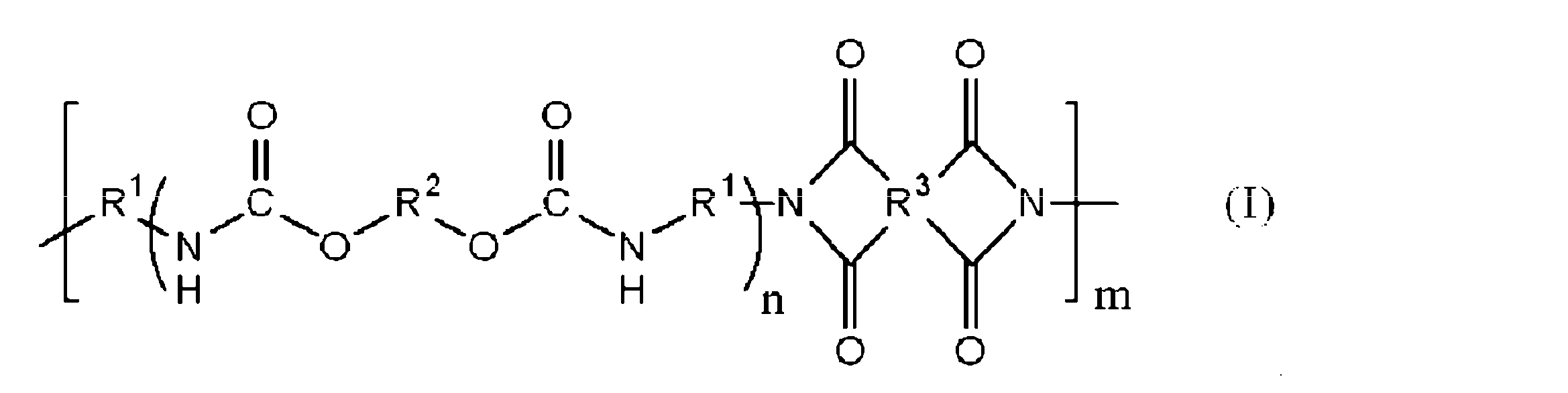
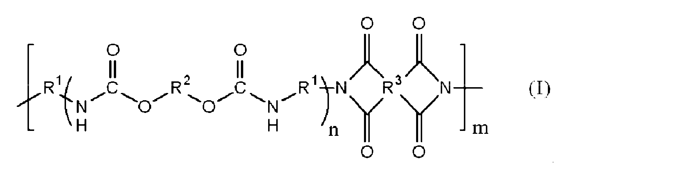
- the present invention comprises a polyurethane imide resin represented by the following general formula (I), a thermosetting resin, a filler, and a printing solvent, and contains a thermosetting resin.
- a die bonding resin paste having an amount of 250 to 500 parts by mass with respect to 100 parts by mass of polyurethaneimide resin is provided.
- R 1 represents a divalent organic group containing an aromatic ring or an aliphatic ring
- R 2 represents a divalent organic group having a molecular weight of 100 to 10,000
- R 3 represents 4 or more carbon atoms.
- a tetravalent organic group containing an atom is shown, and n and m each independently represents an integer of 1 to 100.
- the polyurethaneimide resin represented by the general formula (I) is contained together with a thermosetting resin, a filler and a printing solvent, and a predetermined range of thermosetting resin is blended.
- the tack property can be sufficiently reduced in the B stage state, and the substrates can be directly stacked and stored, and then easily peeled off, and can be used in the subsequent steps.
- the resin paste for die bonding which has the said structure, it can supply and apply
- the filler preferably contains spherical silica fine particles. Thereby, tackiness in the B stage state can be further reduced.
- the present invention also includes a coating step of coating the die bonding resin paste of the present invention on a substrate to form a coating film, and a semiconductor chip mounting step of mounting a semiconductor chip on the coating film.
- An apparatus manufacturing method is provided.
- a semiconductor chip can be attached on a substrate at a relatively low temperature, and excellent heat resistance and chip adhesion. Can be obtained.
- the method for manufacturing a semiconductor device of the present invention further includes a drying step of drying the coating film to form a B-stage after the coating step, and the B-staged coating film on the coating step of the semiconductor chip. It is preferable to mount a semiconductor chip.
- the resin paste for die bonding of the present invention can obtain sufficient heat resistance and chip adhesion in the B-stage state, a semiconductor device with higher reliability can be obtained by including the drying step. .
- the present invention further provides a semiconductor device obtained by the method for manufacturing a semiconductor device of the present invention.
- a semiconductor device can obtain excellent heat resistance and chip adhesiveness because the semiconductor chip is bonded onto the substrate using the die bonding resin paste of the present invention.
- the present invention it is possible to provide a resin paste for die bonding that can be easily supplied and applied by a printing method to a substrate on which a semiconductor chip needs to be attached at a relatively low temperature.
- the resin paste for die bonding of the present invention has heat resistance, is easy to handle, and is excellent in low stress property and low temperature adhesiveness. Further, since the tack property in the B stage state is sufficiently reduced, the substrates can be directly stacked after being made into the B stage, which contributes to the simplification of process management at the time of assembling the semiconductor device.
- the resin paste for die bonding of the present invention can be suitably used for an insulating support substrate such as an organic substrate and a copper lead frame for die bonding, and can also be used for a 42 alloy lead frame. Furthermore, according to the present invention, it is possible to provide a semiconductor device manufacturing method using the die bonding resin paste of the present invention and a semiconductor device manufactured by the manufacturing method.
- the resin bonding for die bonding according to the present invention includes (A) a polyurethaneimide resin represented by the following general formula (I) (hereinafter, “(A) component”) ”)").
- (A) component represents a divalent organic group containing an aromatic ring or an aliphatic ring
- R 2 represents a divalent organic group having a molecular weight of 100 to 10,000
- R 3 represents 4 or more carbon atoms.
- a tetravalent organic group containing an atom is shown, and n and m each independently represents an integer of 1 to 100.
- the resin paste of the present invention comprises (B) a thermosetting resin (hereinafter sometimes referred to as “(B) component”) and (C) filler (hereinafter, “( C) component ”) and (D) a printing solvent (hereinafter sometimes referred to as“ (D) component ”).
- a thermosetting resin hereinafter sometimes referred to as “(B) component”
- C filler
- D a printing solvent
- the polyurethaneimide resin is represented by the above general formula (I).
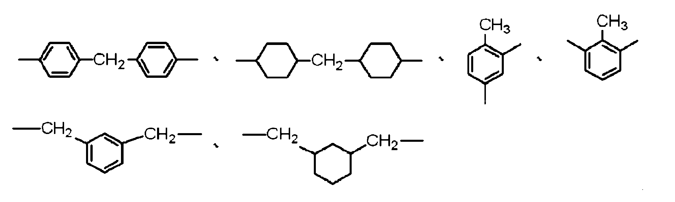
- the divalent organic group containing an aromatic ring or an aliphatic ring represented by R 1 is preferably a diisocyanate residue, and the following general formula (II);
- the structure represented by the formula is more preferably contained in an amount of 10 to 100 mol%.
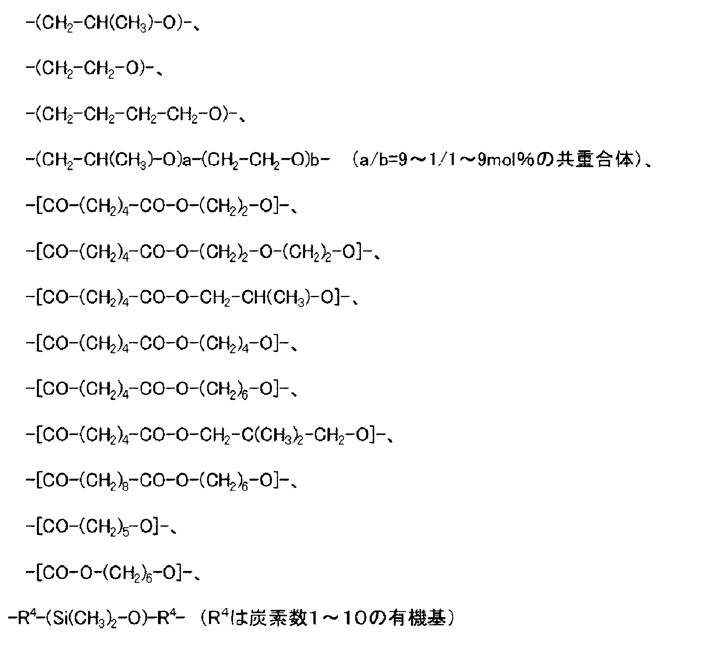
- the divalent organic group having a molecular weight of 100 to 10,000 represented by R 2 in the general formula (I) is preferably a diol residue.
- the diol residue is a group derived from diols such as polybutadiene diol, polyisoprene diol, polycarbonate diol, polyether diol, polyester diol, polycaprolactone diol, and silicone diol.
- R 2 is a diol residue represented by the following general formula (III); More preferably, it contains 10 to 100 mol% of a structure consisting of repeating units represented by:
- the remaining diol residue the following formula: Those having a repeating unit such as These can be used alone or in combination of two or more. These weight average molecular weights are preferably 100 to 10,000, more preferably 500 to 5,000.
- the tetravalent organic group containing 4 or more carbon atoms represented by R 3 in the general formula (I) is preferably a tetracarboxylic acid anhydride residue, represented by the following formula: And groups represented respectively by These can be used alone or in combination of two or more.
- R 3 is more preferably a tetracarboxylic anhydride residue containing 4 to 27 carbon atoms, still more preferably a tetracarboxylic anhydride residue containing 4 to 20 carbon atoms, Particularly preferred is a tetracarboxylic anhydride residue containing 6 to 18 carbon atoms.
- n and m must each independently be an integer of 1 to 100, and more preferably an integer of 1 to 50.
- the polyurethaneimide resin can be synthesized by a usual method such as a solution polymerization method.
- a solution polymerization method diisocyanate and diol are dissolved in a solvent in which the resulting polyurethaneimide resin is dissolved, for example, N-methyl-2-pyrrolidone (NMP), and then at 70 to 180 ° C. for 1 to 5 hours. React to synthesize urethane oligomer. Next, tetracarboxylic dianhydride is added and reacted at 70 ° C. to 180 ° C. for 1 to 10 hours to obtain an NMP solution of polyurethaneimide resin.
- NMP N-methyl-2-pyrrolidone
- the terminal of the polyurethane imide resin can be modified by further adding a monohydric alcohol, oxime, amine, isocyanate, acid anhydride or the like to continue the reaction.
- a monohydric alcohol, oxime, amine, isocyanate, acid anhydride or the like can be used as a catalyst.
- the obtained polyurethane imide resin solution can be separated from the polyurethane imide resin by a reprecipitation method with water or the like according to the purpose.
- the composition ratio of diisocyanate and diol constituting the urethane oligomer is preferably 0.1 to 1.0 mol of the diol component with respect to 1.0 mol of diisocyanate.
- the composition ratio between the polyurethane oligomer constituting the polyurethaneimide resin and the tetracarboxylic dianhydride is preferably 0.1 to 2.0 mol of tetracarboxylic dianhydride with respect to 1.0 mol of the polyurethane oligomer.
- the polyurethaneimide resin (A) preferably has a polystyrene-equivalent weight average molecular weight of 5,000 to 500,000 as measured by gel permeation chromatography using tetrahydrofuran as a solvent. More preferably, it is 000. If the weight average molecular weight is less than 5,000, the strength of the resin tends to be low, and if it exceeds 500,000, the solubility of the resin tends to be poor.
- the blending amount of the component (A) in the resin paste is preferably 10 to 50% by mass based on the total solid content in the resin paste. If this amount exceeds 50% by mass, the curability tends to decrease, and if it is less than 10% by mass, the chip adhesiveness in the B-stage state tends to decrease.
- thermosetting resin for example, an epoxy resin is preferable.
- (B) component you may use the resin mixture containing an epoxy resin, a phenol resin, the compound which has a phenolic hydroxyl group in a molecule
- (B) By containing a thermosetting resin, the resin paste can obtain high reliability after simultaneous curing with the sealing material.
- the epoxy resin contains at least two epoxy groups in the molecule, and phenol glycidyl ether type epoxy resin is preferable from the viewpoint of curability and cured product characteristics.
- phenol glycidyl ether type epoxy resin is preferable from the viewpoint of curability and cured product characteristics.
- resins include bisphenol A, bisphenol AD, bisphenol S, bisphenol F, or a condensate of halogenated bisphenol A and epichlorohydrin, glycidyl ether of phenol novolac resin, glycidyl ether of cresol novolac resin, bisphenol A novolak resin.
- glycidyl ether These can be used individually by 1 type or in combination of 2 or more types.
- the phenol resin has at least two phenolic hydroxyl groups in the molecule, and examples thereof include phenol novolac resin, cresol novolac resin, bisphenol A novolac resin, poly-p-vinylphenol, and phenol aralkyl resin. These can be used individually by 1 type or in combination of 2 or more types.
- thermosetting resin is used in combination with an epoxy resin and a phenol resin or a compound having a phenolic hydroxyl group in the molecule from the viewpoint of the curability and reliability of the cured film. Is preferred.
- the compounding amount of the phenol resin or the compound having a phenolic hydroxyl group in the molecule is preferably 1 to 150 parts by mass, preferably 20 to 120 parts by mass with respect to 100 parts by mass of the epoxy resin. Is more preferably 50 to 100 parts by mass.
- the resin paste of the present invention can contain a curing accelerator together with the epoxy resin from the viewpoint of further improving the curability of the epoxy resin.
- the curing accelerator is not particularly limited as long as it is used for curing the epoxy resin.
- Examples of such a curing accelerator include imidazoles, dicyandiamide derivatives, dicarboxylic acid dihydrazide, triphenylphosphine, tetraphenylphosphonium tetraphenylborate, 2-ethyl-4-methylimidazole-tetraphenylborate, 1,8-diazabicyclo. (5,4,0) undecene-7-tetraphenylborate. These can be used alone or in combination of two or more.
- the blending amount of the curing accelerator is preferably 0.5 to 50 parts by mass, more preferably 1 to 10 parts by mass with respect to 100 parts by mass of the epoxy resin.
- this compounding quantity exceeds 50 mass parts, there exists a possibility that the storage stability of a resin paste may fall.
- thermosetting resin an imide compound having at least two thermosetting imide groups in one molecule can also be used.
- examples of such compounds include orthobismaleimide benzene, metabismaleimide benzene, parabismaleimide benzene, 1,4-bis (p-maleimidocumyl) benzene, 1,4-bis (m-maleimidocumyl).
- examples include benzene. These can be used individually by 1 type or in combination of 2 or more types.
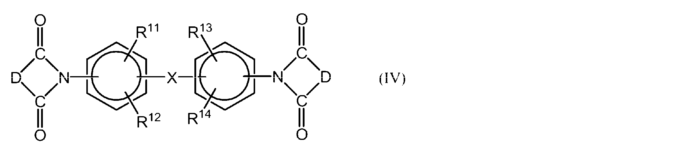
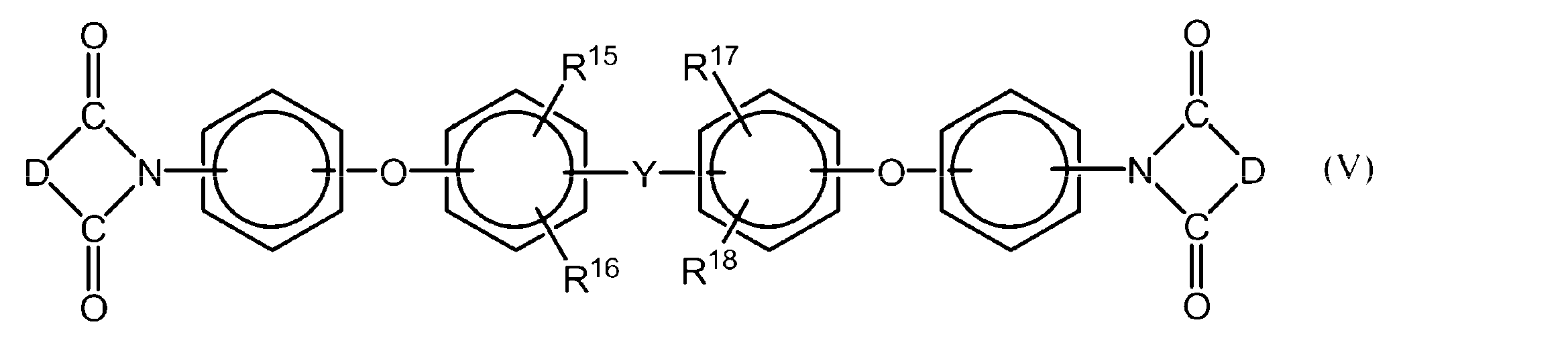
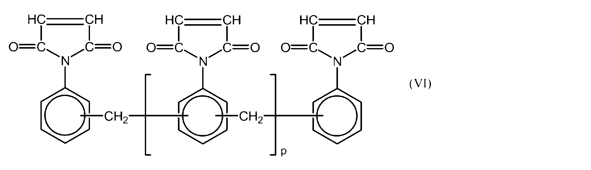
- imide compound it is also preferable to use imide compounds represented by the following general formulas (IV) to (VI).
- X and Y are each independently —O—, —CH 2 —, —CF 2 —, —SO 2 —, —S—, —CO—, —C (CH 3 ) 2 — or —C (CF 3 ) 2 —, wherein R 11 , R 12 , R 13 , R 14 , R 15 , R 16 , R 17 and R 18 are each independently a hydrogen atom, lower alkyl Group, a lower alkoxy group, a fluorine atom, a chlorine atom or a bromine atom, D represents a dicarboxylic acid residue having an ethylenically unsaturated double bond, and p represents an integer of 0 to 4.
- the blending amount of the (B) thermosetting resin needs to be 250 to 500 parts by weight, preferably 260 to 450 parts by weight, and preferably 260 to 370 parts by weight with respect to 100 parts by weight of the component (A). More preferably, it is a part.
- the blending amount is in the range of 250 to 500 parts by mass, the flexibility is excellent, the tack property in the B stage state can be sufficiently reduced, and the hot die shear strength can be improved.
- filler (C) examples include conductive (metal) fillers such as silver powder, gold powder, and copper powder; inorganic fillers such as silica, alumina, titania, glass, iron oxide, and ceramic.
- conductive (metal) fillers such as silver powder, gold powder, and copper powder
- inorganic fillers such as silica, alumina, titania, glass, iron oxide, and ceramic.
- conductive (metal) fillers such as silver powder, gold powder, and copper powder are added for the purpose of imparting conductivity, heat conductivity, or thixotropy to the adhesive.
- inorganic fillers such as silica, alumina, titania, glass, iron oxide, and ceramic are added for the purpose of imparting low thermal expansion, low moisture absorption, and thixotropy to the adhesive. These can be used individually by 1 type or in combination of 2 or more types.
- an inorganic ion exchanger as a filler which improves the electrical reliability of a semiconductor device.
- the inorganic ion exchanger ions extracted from an aqueous solution when the paste cured product is extracted in hot water, for example, ion traps such as Na + , K + , Cl ⁇ , F ⁇ , RCOO ⁇ , Br ⁇ , etc. Those whose action is recognized are effective.
- ion exchangers include naturally occurring zeolites, natural minerals such as zeolites, acid clay, dolomite, hydrotalcites, artificially synthesized synthetic zeolites, and the like.
- conductive fillers or inorganic fillers can be used alone or in combination of two or more.
- one or more kinds of conductive fillers and one or more kinds of inorganic fillers may be mixed and used as long as the physical properties are not impaired.
- spherical silica fine particles are contained as the component (C) from the viewpoint of improving printability and further reducing tack.
- the average particle diameter of the spherical silica fine particles is preferably 50 nm to 2000 nm, more preferably 100 nm to 1000 nm, and further preferably 200 nm to 800 nm.
- the blending amount of the (C) filler is preferably 1 to 200 parts by mass, more preferably 30 to 170 parts by mass, and 60 to 140 parts by mass with respect to 100 parts by mass of the component (A). Is particularly preferred.
- the blending amount of the filler is preferably 1 part by mass or more from the viewpoint of imparting sufficient thixotropic property (for example, thixotropy index: 1.5 or more) to the resin paste.
- the blending amount of the filler is preferably 200 parts by mass or less from the viewpoint of printability and adhesiveness. When the blending amount exceeds 200 parts by mass, the elastic modulus of the cured product is increased, and as a result, die bonding is performed. There is a possibility that the stress relaxation ability of the material is lowered and the mounting reliability of the semiconductor device is lowered.
- the printing solvent which is component (D) is preferably selected from (C) solvents that can uniformly knead or disperse the filler. In view of preventing solvent volatilization during printing, it is preferable to select a solvent having a boiling point of 100 ° C. or higher. (D) The viscosity of the resin paste can be adjusted by the printing solvent.
- Examples of the printing solvent include N-methyl-2-pyrrolidinone, diethylene glycol dimethyl ether (also referred to as diglyme), triethylene glycol dimethyl ether (also referred to as triglyme), diethylene glycol diethyl ether, 2- (2-methoxyethoxy) ethanol, ⁇ -Butyrolactone, isophorone, carbitol, carbitol acetate, 1,3-dimethyl-2-imidazolidinone, 2- (2-butoxyethoxy) ethyl acetate, ethyl cellosolve, ethyl cellosolve acetate, butyl cellosolve, dioxane, cyclohexanone, anisole
- a solvent mainly composed of petroleum distillate used as a solvent for printing ink can be mentioned. These can be used individually by 1 type or in mixture of 2 or more types.
- the blending amount of the printing solvent (D) is preferably 30 to 90% by mass, more preferably 35 to 75% by mass, and 40 to 60% by mass, based on the solid content of the resin paste. Particularly preferred.
- the solid content is 30% by mass or more, it is preferable from the viewpoint of shape change suppression based on a decrease in volume after drying the paste, and when it is 90% by mass or less, it is preferable from the viewpoint of improvement in paste fluidity and printing workability.
- the amount added thereof is preferably 0.01% by mass or more based on the total amount of the printing solvent and the additive, and adhesion and viscosity stability of the paste. In view of the above, it is preferably 10% by mass or less.
- the resin paste contains a butadiene homopolymer or copolymer having a carboxylic acid end group, a silane coupling agent, a titanium coupling agent, a nonionic surfactant, a fluorine surfactant.
- silicone additives and the like may be added as appropriate.
- butadiene homopolymers or copolymers having carboxylic acid end groups include, for example, “Hycer CTBN-2009 ⁇ 162”, “CTBN-1300”, which is a low molecular weight liquid polybutadiene having acrylonitrile introduced into the main chain and having a carboxylic acid at the terminal.
- CTBN-1300 ⁇ 8 a low molecular weight liquid polybutadiene having acrylonitrile introduced into the main chain and having a carboxylic acid at the terminal.
- ⁇ 31 “ CTBN-1300 ⁇ 8 ”,“ CTBN-1300 ⁇ 13 ”,“ CTBNX-1300 ⁇ 9 ”(all manufactured by Ube Industries, Ltd.) and low molecular weight liquid polybutadiene having a carboxylic acid group
- NISSO-PB-C-2000 manufactured by Nippon Soda Co., Ltd.
- the thixotropy index of the resin paste is preferably 1.0 to 8.0.
- the thixotropy index of the resin paste is 1.0 or more, the occurrence of sagging or the like in the paste supplied and applied by the printing method tends to be suppressed, and the printed shape tends to be kept good.
- the thixotropy index is 8.0 or less, it tends to be possible to suppress the occurrence of “chips” or scumming in the paste supplied and applied by the printing method.
- the viscosity (25 ° C.) of the resin paste is preferably 1 to 1000 Pa ⁇ s.
- the viscosity of the resin paste is preferably adjusted as appropriate according to the type of printing method. In the case of a stencil plate or the like, it is preferably adjusted in the range of 20 to 500 Pa ⁇ s. Moreover, when many voids remain in the paste after drying, it is effective to adjust the viscosity to 150 Pa ⁇ s or less.
- the above viscosity is a value measured using an E-type rotational viscometer under the conditions of 25 ° C. and a rotational speed of 0.5 rpm.
- the resulting resin paste for die bonding includes a lead frame such as a 42 alloy lead frame or a copper lead frame; or a plastic film such as a polyimide resin, an epoxy resin, or a polyimide resin; A resin, epoxy resin, polyimide resin or other plastic impregnated and cured; or a ceramic support member such as alumina can be supplied and applied by a printing method to form a B stage. Thereby, a support substrate with a B stage adhesive is obtained. A semiconductor element (chip) such as an IC or LSI is attached to the support substrate with the B stage adhesive, and the chip is bonded to the support substrate by heating. Thereafter, the chip is mounted on the support substrate by a step of post-curing the resin paste. This post-curing of the resin paste may be performed together with the post-curing process of the sealing material when there is no problem in the mounting assembly process.
- a lead frame such as a 42 alloy lead frame or a copper lead frame
- a plastic film such as a polyimide resin,
- the method for manufacturing a semiconductor device according to the present invention preferably includes at least a coating step of applying a resin paste on a substrate to form a coating film, and a semiconductor chip mounting step of mounting a semiconductor chip on the coating film.
- a method that further includes a drying step of drying the coating film to form a B-stage after the coating step and more specifically includes the above-described steps.
- the semiconductor device according to the present invention is manufactured by a manufacturing method including the above steps.
- the die bonding resin paste contains a solvent, but when used in a semiconductor device manufacturing method, most of the solvent is volatilized by forming a B stage in the drying process. It is possible to assemble a semiconductor device with a small amount and good mounting reliability.
- the semiconductor element can be attached without drying and semi-curing, and then the chip can be bonded to the support substrate by heating. .
- another method of manufacturing a semiconductor device according to the present invention includes the steps of applying a predetermined amount of the above-mentioned die bonding resin paste on a substrate and mounting the semiconductor chip on the resin paste.
- the semiconductor device according to the invention is manufactured by a manufacturing method including the above steps.
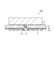
- FIG. 1 is a schematic cross-sectional view showing an embodiment of a semiconductor device (a substrate having a BOC structure for memory) of the present invention.
- a semiconductor chip 2 such as an IC chip is bonded to a substrate 6 having solder balls 8 via an adhesive 4 made of a resin paste for die bonding of the present invention.
- the solder balls 8 are formed on the circuit layer 14 formed on the surface of the substrate 6.
- a resist layer 16 is formed on the circuit layer 14.
- the semiconductor device 100 has a configuration in which the connection terminal of the semiconductor chip 2 is electrically connected to the substrate 6 via a wire 10 such as a gold wire and is further sealed with a sealing resin 12.
- cresol novolac type epoxy resin (trade name: YDCN-702S, manufactured by Toto Kasei Co., Ltd., epoxy equivalent 200), bisphenol A novolak resin (trade name: VH-4170, Dainippon Ink and Chemicals, Inc.) Co., Ltd., OH equivalent 118) 9.9 parts by mass of a carbitol acetate (36 parts by mass) solution was prepared.
- tetraphenylphosphonium tetraphenylborate (trade name: TPPK, manufactured by Tokyo Chemical Industry Co., Ltd.), Aerosil (trade name: AEROSIL 380, manufactured by Nippon Aerosil Co., Ltd., bulk silica fine particles), silica (trade name) : SO-C2, manufactured by Admatechs Co., Ltd., spherical silica fine particles, average particle diameter of 500 nm) were prepared.
- Examples 1 to 3 and Comparative Examples 1 to 3 3 die bonding resin paste was obtained.
- the amount of carbitol acetate (CA) in Table 1 indicates the amount of carbitol acetate contained as a solvent in the polyurethaneimide resin solution and in the epoxy resin and phenol resin carbitol acetate solutions. ing.
- the sticking property (tack property) after the resist coated substrate was pressure-bonded in the B stage state was evaluated.
- the evaluation method of sticking property is as follows.
- the resin pastes produced in the examples and comparative examples were applied to an evaluation substrate and dried by heating in an oven at 110 ° C. for 1 hour to form a B-stage coating film (die bonding layer).
- the evaluation substrate is obtained by applying a solder resist AUS-308 (manufactured by Dainippon Ink) to an MCL-E679F substrate (manufactured by Hitachi Chemical Co., Ltd.). Thereafter, a 10 mm ⁇ 12 mm evaluation substrate was pressure-bonded on the die bonding layer for 60 seconds on a 30 ° C.
- Table 1 shows the results. In Table 1, “A” indicates that the substrate was dropped without being bonded after the pressure bonding, and “B” indicates that the substrate was still bonded after the pressure bonding.
- the method for measuring the die shear strength during heating is as follows.
- the resin pastes produced in the examples and comparative examples were printed on 42 alloy lead frames and dried in an oven at 110 ° C. for 60 minutes. Thereafter, a 5 ⁇ 5 mm silicon chip (thickness: 0.5 mm) was applied onto the resin paste by applying a load of 5 kgf on a 200 ° C. heating plate for 1 second, and heated and cured in an oven at 180 ° C. for 60 minutes. .
- the resin pastes (Examples 1 to 3) of the present invention have sufficiently reduced tackiness at room temperature after B-staging, and conventional resin pastes (Comparative Examples 1 to 3). It was found that the substrate can be transported in a state where the substrates are directly stacked. Further, it was found that the resin paste according to the present invention has a high thermal shear strength at 250 ° C. after the chip is pressure-bonded and post-cured, and has high chip adhesion and heat resistance. .
Landscapes
- Chemical & Material Sciences (AREA)
- Organic Chemistry (AREA)
- Chemical Kinetics & Catalysis (AREA)
- Health & Medical Sciences (AREA)
- Medicinal Chemistry (AREA)
- Polymers & Plastics (AREA)
- Materials Engineering (AREA)
- Life Sciences & Earth Sciences (AREA)
- Engineering & Computer Science (AREA)
- Wood Science & Technology (AREA)
- Inorganic Chemistry (AREA)
- Die Bonding (AREA)
- Adhesives Or Adhesive Processes (AREA)
- Compositions Of Macromolecular Compounds (AREA)
- Macromolecular Compounds Obtained By Forming Nitrogen-Containing Linkages In General (AREA)
Abstract
Description



ジフェニルメタン-4,4’-ジイソシアネート(1.0mol)、ジフェニルメタン-2,4’-ジイソシアネート(1.0mol)、及び、重量平均分子量1,000のポリテトラメチレングリコール(0.8mol)を、1-メチル-2-ピロリドン(以下、「NMP」という)中で窒素雰囲気下、100℃で1時間反応させた後、そこに、4,4’-オキシジフタル酸無水物(1.0mol)、NMP(60.0mol)を添加し、さらに100℃で3時間攪拌した。次いで、さらにベンジルアルコール(0.49mol)を添加して100℃で1時間攪拌し、反応を終了した。得られた溶液を激しく攪拌させた水に入れ、生成した沈殿物を濾別し、それを真空中、80℃で8時間乾燥させ、ポリウレタンイミド樹脂を得た。得られたポリウレタンイミド樹脂を、GPCを用いて測定した結果、ポリスチレン換算で、Mw=93,700、Mn=38,800であった。また、得られたポリウレタンイミド樹脂を固形分濃度40質量%でカルビトールアセテート(CA)に溶解し、ポリウレタンイミド樹脂溶液を得た。

Claims (5)
- 下記一般式(I)で表されるポリウレタンイミド樹脂と、熱硬化性樹脂と、フィラーと、印刷用溶剤と、を含有し、
前記熱硬化性樹脂の配合量が、前記ポリウレタンイミド樹脂100質量部に対し、250~500質量部である、ダイボンディング用樹脂ペースト。

- 前記フィラーが、球状シリカ微粒子を含む、請求項1記載のダイボンディング用樹脂ペースト。
- 基板上に請求項1又は2記載のダイボンディング用樹脂ペーストを塗布して塗膜を形成する塗布工程と、
前記塗膜上に半導体チップを搭載する半導体チップ搭載工程と、
を含む、半導体装置の製造方法。 - 前記塗布工程の後に、前記塗膜を乾燥してBステージ化する乾燥工程を更に含み、
前記半導体チップ搭載工程において、Bステージ化した前記塗膜上に半導体チップを搭載する、請求項3記載の半導体装置の製造方法。 - 請求項3又は4記載の半導体装置の製造方法により得られる半導体装置。
Priority Applications (3)
| Application Number | Priority Date | Filing Date | Title |
|---|---|---|---|
| JP2010542897A JPWO2010070947A1 (ja) | 2008-12-17 | 2009-07-24 | ダイボンディング用樹脂ペースト、半導体装置の製造方法及び半導体装置 |
| CN2009801502835A CN102246285A (zh) | 2008-12-17 | 2009-07-24 | 芯片接合用树脂糊料、半导体装置的制造方法以及半导体装置 |
| SG2011043411A SG172144A1 (en) | 2008-12-17 | 2009-07-24 | Resin paste for die bonding, method for producing semiconductor device, and semiconductor device |
Applications Claiming Priority (2)
| Application Number | Priority Date | Filing Date | Title |
|---|---|---|---|
| JP2008-321123 | 2008-12-17 | ||
| JP2008321123 | 2008-12-17 |
Publications (1)
| Publication Number | Publication Date |
|---|---|
| WO2010070947A1 true WO2010070947A1 (ja) | 2010-06-24 |
Family
ID=42268625
Family Applications (1)
| Application Number | Title | Priority Date | Filing Date |
|---|---|---|---|
| PCT/JP2009/063283 Ceased WO2010070947A1 (ja) | 2008-12-17 | 2009-07-24 | ダイボンディング用樹脂ペースト、半導体装置の製造方法及び半導体装置 |
Country Status (6)
| Country | Link |
|---|---|
| JP (1) | JPWO2010070947A1 (ja) |
| KR (1) | KR20110050561A (ja) |
| CN (1) | CN102246285A (ja) |
| SG (1) | SG172144A1 (ja) |
| TW (1) | TW201026806A (ja) |
| WO (1) | WO2010070947A1 (ja) |
Cited By (3)
| Publication number | Priority date | Publication date | Assignee | Title |
|---|---|---|---|---|
| CN101906248A (zh) * | 2010-07-08 | 2010-12-08 | 浙江大学 | 高压缩强度刚性增强型硬质聚氨酯泡沫塑料及其制备方法 |
| JP2012097232A (ja) * | 2010-11-04 | 2012-05-24 | Kaneka Corp | ボンディングシート |
| JP2017168840A (ja) * | 2017-03-11 | 2017-09-21 | 日揮触媒化成株式会社 | 半導体装置実装用ペ−ストの製造方法 |
Families Citing this family (2)
| Publication number | Priority date | Publication date | Assignee | Title |
|---|---|---|---|---|
| JP5741809B2 (ja) * | 2011-02-22 | 2015-07-01 | 三菱マテリアル株式会社 | 接合用ペースト、および半導体素子と基板の接合方法 |
| KR102012788B1 (ko) * | 2015-09-23 | 2019-08-21 | 주식회사 엘지화학 | 접착 필름, 반도체 장치의 제조 방법 및 반도체 장치 |
Citations (1)
| Publication number | Priority date | Publication date | Assignee | Title |
|---|---|---|---|---|
| WO2008041646A1 (fr) * | 2006-10-04 | 2008-04-10 | Hitachi Chemical Company, Ltd. | Pâte résineuse pour fixation de puce, procédé de fabrication d'un dispositif semi-conducteur et dispositif semi-conducteur |
Family Cites Families (3)
| Publication number | Priority date | Publication date | Assignee | Title |
|---|---|---|---|---|
| JP4604682B2 (ja) * | 2004-01-08 | 2011-01-05 | 日立化成工業株式会社 | ポリウレタンイミド樹脂及びこれを用いた接着剤組成物 |
| JP2006241174A (ja) * | 2005-02-07 | 2006-09-14 | Hitachi Chem Co Ltd | ダイボンディング用フィルム状接着剤及びこれを用いた接着シート、並びに半導体装置。 |
| KR20080030581A (ko) * | 2005-05-31 | 2008-04-04 | 스미토모 베이클리트 컴퍼니 리미티드 | 프리어플리케이션용 봉지 수지 조성물, 이를 이용한반도체장치 및 그 제조방법 |
-
2009
- 2009-07-24 CN CN2009801502835A patent/CN102246285A/zh active Pending
- 2009-07-24 SG SG2011043411A patent/SG172144A1/en unknown
- 2009-07-24 JP JP2010542897A patent/JPWO2010070947A1/ja active Pending
- 2009-07-24 KR KR1020117007854A patent/KR20110050561A/ko not_active Ceased
- 2009-07-24 WO PCT/JP2009/063283 patent/WO2010070947A1/ja not_active Ceased
- 2009-08-17 TW TW098127608A patent/TW201026806A/zh unknown
Patent Citations (1)
| Publication number | Priority date | Publication date | Assignee | Title |
|---|---|---|---|---|
| WO2008041646A1 (fr) * | 2006-10-04 | 2008-04-10 | Hitachi Chemical Company, Ltd. | Pâte résineuse pour fixation de puce, procédé de fabrication d'un dispositif semi-conducteur et dispositif semi-conducteur |
Cited By (3)
| Publication number | Priority date | Publication date | Assignee | Title |
|---|---|---|---|---|
| CN101906248A (zh) * | 2010-07-08 | 2010-12-08 | 浙江大学 | 高压缩强度刚性增强型硬质聚氨酯泡沫塑料及其制备方法 |
| JP2012097232A (ja) * | 2010-11-04 | 2012-05-24 | Kaneka Corp | ボンディングシート |
| JP2017168840A (ja) * | 2017-03-11 | 2017-09-21 | 日揮触媒化成株式会社 | 半導体装置実装用ペ−ストの製造方法 |
Also Published As
| Publication number | Publication date |
|---|---|
| JPWO2010070947A1 (ja) | 2012-05-24 |
| CN102246285A (zh) | 2011-11-16 |
| KR20110050561A (ko) | 2011-05-13 |
| SG172144A1 (en) | 2011-07-28 |
| TW201026806A (en) | 2010-07-16 |
Similar Documents
| Publication | Publication Date | Title |
|---|---|---|
| JP5360124B2 (ja) | ダイボンディング用樹脂ペーストおよびその用途 | |
| CN101542719A (zh) | 倒装芯片半导体封装件用接合体、积层材料、密封树脂组合物和电路基板 | |
| JP5225853B2 (ja) | ダイボンディング用樹脂ペースト、半導体装置の製造方法及び半導体装置 | |
| WO2010110069A1 (ja) | ダイボンディング用樹脂ペースト、それを用いた半導体装置の製造方法、及び半導体装置 | |
| CN103031091A (zh) | 芯片接合用树脂糊、半导体装置的制造方法和半导体装置 | |
| JP5157938B2 (ja) | ダイボンディング用樹脂ペースト、該樹脂ペーストを用いた半導体装置の製造方法、および該製造方法により得られる半導体装置 | |
| WO2010070947A1 (ja) | ダイボンディング用樹脂ペースト、半導体装置の製造方法及び半導体装置 | |
| JP4816876B2 (ja) | ダイボンディング用樹脂ペーストおよび半導体装置の製造方法 | |
| JP2008112972A (ja) | ダイボンディング用樹脂ペースト、半導体装置の製造方法及び半導体装置 | |
| JP5130682B2 (ja) | ダイボンディング用樹脂ペースト、該樹脂ペーストを用いた半導体装置の製造方法、および該製造方法により得られる半導体装置 | |
| JP2008277803A (ja) | ダイボンディング用樹脂ペースト組成物、それを用いた半導体装置の製造方法及び半導体装置 | |
| JP2008509241A (ja) | 電子デバイス用の低空孔で非流動性のフラクシングアンダーフィル | |
| JP2013170254A (ja) | ダイボンディング用樹脂ペースト、半導体装置の製造方法及び半導体装置 | |
| JP2002161192A (ja) | 半導体装置 | |
| JP2007110099A (ja) | ダイボンディング材及びダイボンディング材用樹脂ペースト |
Legal Events
| Date | Code | Title | Description |
|---|---|---|---|
| WWE | Wipo information: entry into national phase |
Ref document number: 200980150283.5 Country of ref document: CN |
|
| 121 | Ep: the epo has been informed by wipo that ep was designated in this application |
Ref document number: 09833253 Country of ref document: EP Kind code of ref document: A1 |
|
| WWE | Wipo information: entry into national phase |
Ref document number: 2010542897 Country of ref document: JP |
|
| ENP | Entry into the national phase |
Ref document number: 20117007854 Country of ref document: KR Kind code of ref document: A |
|
| NENP | Non-entry into the national phase |
Ref country code: DE |
|
| 122 | Ep: pct application non-entry in european phase |
Ref document number: 09833253 Country of ref document: EP Kind code of ref document: A1 |