WO2010067706A1 - 非接触情報媒体 - Google Patents
非接触情報媒体 Download PDFInfo
- Publication number
- WO2010067706A1 WO2010067706A1 PCT/JP2009/069849 JP2009069849W WO2010067706A1 WO 2010067706 A1 WO2010067706 A1 WO 2010067706A1 JP 2009069849 W JP2009069849 W JP 2009069849W WO 2010067706 A1 WO2010067706 A1 WO 2010067706A1
- Authority
- WO
- WIPO (PCT)
- Prior art keywords
- contact information
- information medium
- coil
- region
- main loop
- Prior art date
- Legal status (The legal status is an assumption and is not a legal conclusion. Google has not performed a legal analysis and makes no representation as to the accuracy of the status listed.)
- Ceased
Links
Images




Classifications
-
- G—PHYSICS
- G06—COMPUTING OR CALCULATING; COUNTING
- G06K—GRAPHICAL DATA READING; PRESENTATION OF DATA; RECORD CARRIERS; HANDLING RECORD CARRIERS
- G06K19/00—Record carriers for use with machines and with at least a part designed to carry digital markings
- G06K19/06—Record carriers for use with machines and with at least a part designed to carry digital markings characterised by the kind of the digital marking, e.g. shape, nature, code
- G06K19/067—Record carriers with conductive marks, printed circuits or semiconductor circuit elements, e.g. credit or identity cards also with resonating or responding marks without active components
- G06K19/07—Record carriers with conductive marks, printed circuits or semiconductor circuit elements, e.g. credit or identity cards also with resonating or responding marks without active components with integrated circuit chips
- G06K19/077—Constructional details, e.g. mounting of circuits in the carrier
- G06K19/07749—Constructional details, e.g. mounting of circuits in the carrier the record carrier being capable of non-contact communication, e.g. constructional details of the antenna of a non-contact smart card
-
- H—ELECTRICITY
- H01—ELECTRIC ELEMENTS
- H01Q—ANTENNAS, i.e. RADIO AERIALS
- H01Q7/00—Loop antennas with a substantially uniform current distribution around the loop and having a directional radiation pattern in a plane perpendicular to the plane of the loop
- H01Q7/005—Loop antennas with a substantially uniform current distribution around the loop and having a directional radiation pattern in a plane perpendicular to the plane of the loop with variable reactance for tuning the antenna
-
- H—ELECTRICITY
- H04—ELECTRIC COMMUNICATION TECHNIQUE
- H04B—TRANSMISSION
- H04B5/00—Near-field transmission systems, e.g. inductive or capacitive transmission systems
- H04B5/40—Near-field transmission systems, e.g. inductive or capacitive transmission systems characterised by components specially adapted for near-field transmission
- H04B5/48—Transceivers
-
- H—ELECTRICITY
- H04—ELECTRIC COMMUNICATION TECHNIQUE
- H04B—TRANSMISSION
- H04B5/00—Near-field transmission systems, e.g. inductive or capacitive transmission systems
- H04B5/20—Near-field transmission systems, e.g. inductive or capacitive transmission systems characterised by the transmission technique; characterised by the transmission medium
- H04B5/24—Inductive coupling
-
- H—ELECTRICITY
- H04—ELECTRIC COMMUNICATION TECHNIQUE
- H04B—TRANSMISSION
- H04B5/00—Near-field transmission systems, e.g. inductive or capacitive transmission systems
- H04B5/70—Near-field transmission systems, e.g. inductive or capacitive transmission systems specially adapted for specific purposes
- H04B5/77—Near-field transmission systems, e.g. inductive or capacitive transmission systems specially adapted for specific purposes for interrogation
Definitions
- the present invention relates to a non-contact information medium that exchanges information with the outside by using radio waves.
- the coil antenna used for exchanging information using electromagnetic induction is constituted by a resonance circuit, and usually the resonance frequency is adjusted (tuned) in order to efficiently exchange information.
- Important parameters that determine the resonant frequency of the resonant circuit include the self-inductance and capacitance of the resonant circuit.
- the resonance frequency is usually adjusted by changing these self-inductance and capacitance values.
- one of the applications using a coil antenna is a non-contact information medium. Since the non-contact information medium is not in contact with the reader / writer, it does not cause a contact failure and can be used at a position away from the reader / writer. In addition, the non-contact method has features such as resistance to dirt, rain, and static electricity, and demand is increasing due to its high security level.
- the non-contact information medium obtains operating power by electromagnetic induction using radio waves received from the reader / writer, and exchanges information with the reader / writer using radio waves of a predetermined frequency. For this reason, the non-contact information medium and the reader / writer have a built-in coil antenna for transmitting and receiving radio waves of a predetermined frequency.
- a conventional non-contact information medium basically includes a coil that forms a loop antenna that receives power from outside and transmits and receives information, a capacitor that forms a resonance circuit with the coil, and a non-contact And an IC chip for controlling the processing operation of the information medium.
- the non-contact information medium is disposed within a communication range near the reader / writer. As a result, interaction occurs between the resonance circuit of the non-contact information medium and the resonance circuit of the reader / writer, and an induced current is generated in the coil forming the loop antenna of the non-contact information medium.
- the IC chip uses this induced current as an operating power supply to operate and transmits information to the reader / writer via a coil forming a loop antenna.
- the non-contact information medium and the reader / writer perform wireless communication to transmit / receive information (see, for example, Patent Document 1).
- a chip coil (lumped constant type inductor) is provided in a part of the coil of the non-contact information medium to reduce the interaction between the non-contact information medium and the frequency of the radio wave used for communication.
- a technique for improving the reading performance when a plurality of non-contact information media are arranged in the vicinity of the reader / writer by matching the resonance frequency of the non-contact information medium is disclosed (for example, see Patent Document 2). ).
- the present invention has been made in view of the above, and even when a large number of identical objects are stacked, information can be exchanged with the outside via radio waves individually and reliably.
- An object is to provide a suitable non-contact information medium.
- a non-contact information medium includes a main loop that circulates an outer edge of a predetermined region on a plane over substantially the entire circumference, and the main loop on the plane.
- a loop antenna that is wound around a region having a smaller area than a region surrounding the main loop, and has a coil connected in series to the main loop, and transmits and receives radio waves to and from the outside, and a capacitor connected in parallel to the main loop
- an IC chip that is connected in parallel to the capacitor and receives a radio wave propagated from outside and transmits a radio wave responding to the received radio wave to the outside, and passes through the plane within the predetermined area.
- a pattern having a rotational symmetry of 180 degrees about a single straight line orthogonal to the plane is formed, and overlaps the coil along a direction orthogonal to the plane.
- the loop antenna includes a plurality of the coils, and the arrangement pattern of the plurality of coils has a rotational symmetry of 180 degrees with respect to the rotation axis. It is characterized by having.
- the non-contact information medium according to the present invention has a plate shape according to the above invention, and the loop antenna, the capacitor, the IC chip, and the electric conductor are provided on any of the surfaces parallel to the plane. It further comprises a substrate.
- the non-contact information medium according to the present invention is characterized in that, in the above invention, the base material has a rotational symmetry of 180 degrees with respect to the rotation axis together with the arrangement pattern of the electric conductor.
- the base material has a shape having a rotational symmetry of 180 degrees with at least one straight line passing through any one of the surfaces as a second rotation axis.
- the coil moves to a region where the coil is located before the rotation and a region which does not overlap along a direction perpendicular to the surface.
- the present invention since the surfaces of the coil and the electric conductor overlap each other along a predetermined direction, when two non-contact information media overlap, either one of the non-contact information media
- the coil included in is placed between the electric conductor of its own and the electric conductor of another non-contact information medium.
- the self-inductance of the coil sandwiched between the two electric conductors decreases, and the resonance frequency of the resonance circuit constituted by the coil and the capacitor increases.
- the resonance frequency of the resonance circuit is once raised, even if the resonance frequency is gradually lowered by further overlapping the non-contact information medium thereafter, reading is performed from the outside.
- the number of sheets can be increased more than before until the minimum possible value is reached. Therefore, even when many identical objects are stacked, information can be exchanged with the outside via radio waves individually and reliably.
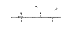
- FIG. 1 is a plan view showing a configuration of a non-contact information medium according to Embodiment 1 of the present invention.
- 2 is a cross-sectional view taken along line AA in FIG.
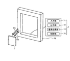
- FIG. 3 is a diagram showing a configuration of a reader / writer that reads information recorded by the non-contact information medium according to Embodiment 1 of the present invention.
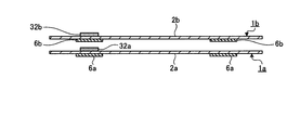
- FIG. 4 is a diagram illustrating a state in which two non-contact information media according to Embodiment 1 of the present invention are stacked.
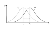
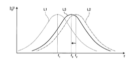
- FIG. 5 is a diagram schematically showing a change in the resonance frequency of the resonance circuit of the non-contact information medium when two sheets are stacked.
- FIG. 6 is a diagram illustrating a state in which three non-contact information media according to Embodiment 1 of the present invention are stacked.
- FIG. 7 is a diagram schematically showing a change in the resonance frequency of the resonance circuit of the non-contact information medium when three sheets are stacked.
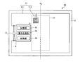
- FIG. 8 is a plan view showing a configuration of a non-contact information medium according to a modification of the first embodiment of the present invention.
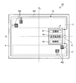
- FIG. 9 is a plan view showing the configuration of the non-contact information medium according to Embodiment 2 of the present invention.
- FIG. 10 is a plan view showing a configuration of a non-contact information medium according to a modification of the second embodiment of the present invention.
- FIG. 11 is a plan view showing the configuration of the non-contact information medium according to Embodiment 3 of the present invention.
- FIG. 1 is a plan view showing a configuration of a non-contact information medium according to Embodiment 1 of the present invention.
- 2 is a cross-sectional view taken along line AA in FIG.
- the non-contact information medium 1 shown in these figures includes a plate-like base material 2 having a rectangular surface, a loop antenna 3 that receives a radio wave propagating from the outside and transmits a radio wave that responds to the radio wave.
- the capacitor 4 connected in parallel to the loop antenna 3, the IC chip 5 connected in parallel to the capacitor 4, and the two electric conductors 6 provided on the other surface of the substrate 2 are provided.
- the substrate 2 has a rotational symmetry of 180 degrees with a straight line that is parallel to the long side of the surface rectangle and passes through the center of the rectangle as the rotation axis O 1 . Further, the substrate 2, a straight line passing through the are and the center of the rectangle parallel to the rectangular shorter sides of the surface as a rotation axis O 2 having a rotational symmetry of 180 degrees. That is, the rotation axes O 1 and O 2 correspond to the second rotation axis.
- the loop antenna 3 is formed on the surface of the base material 2 by, for example, etching a conductor, and includes a main loop 31 composed of a conductive wire that circulates around the outer periphery of the base material 2 over substantially the entire periphery, and a region surrounding the main loop 31. And a coil 32 connected to the main loop 31 in series.
- the coil 32 is formed of a conductive wire wound in a square spiral shape in a small area.
- the coil 32 located in the upper left region of the substrate 2 in FIG. 1 moves to the lower left region of the substrate 2 by rotating 180 degrees around the rotation axis O 1 while rotating.
- the substrate 2 is moved to the upper right region by rotating 180 degrees around the axis O 2 .
- the main loop 31 has one winding of the conductive wire, and has a smaller self-inductance than the case of having a plurality of main loops as in the technique described in Patent Document 1. For this reason, the self-inductance value of the entire loop antenna 3 is adjusted by the self-inductance of the coil 32.
- the shape of the main loop 31 can be changed as appropriate according to the shape of the substrate 2.
- the winding shape of the coil 32 may also be a spiral shape other than a square.
- the capacitor 4 is provided on the inner peripheral side of the main loop 31 on the surface of the base material 2 on which the loop antenna 3 is provided, and is connected in parallel to the main loop 31.
- the capacitor 4 forms a resonance circuit with the loop antenna 3.
- the IC chip 5 is provided on the inner peripheral side of the main loop 31 on the surface of the base material 2 on which the loop antenna 3 is provided.
- the IC chip 5 receives a signal based on a radio wave propagated from the outside and received by the loop antenna 3 and stores various information including identification information for identifying the non-contact information medium 1, and the received signal Includes a signal processing unit 52 that reads information corresponding to a request included in the storage unit 51, transmits a signal corresponding to the read information to the loop antenna 3, and a control unit 53 that controls the operation of the IC chip. .
- the IC chip 5 starts its operation when it reaches a voltage that can be operated by an induced current generated according to a radio wave propagated from the outside.
- the two electric conductors 6 are realized by a thin film metal or the like, and are provided on a part of the surface (the back side in FIG. 1) different from the surface on which the loop antenna 3 or the like is provided among the surfaces of the base material 2. Yes.
- the surface of each electric conductor 6 has a rectangular shape, and the longitudinal direction thereof is arranged in parallel with the short direction of the substrate 2.
- the two electric conductors 6 pass through a rectangular center (intersection of the rotation axes O 1 and O 2 ) forming the surface of the substrate 2 and are 180 degrees with a straight line orthogonal to the surface as the rotation axis O 3 . It has a pattern with rotational symmetry.
- the electric conductor 6 overlaps with the coil 32 along a direction orthogonal to the surface of the substrate 2. Since the electrical conductor 6 and the coil 32 have the above-described positional relationship, when a magnetic flux is generated in the coil 32, an eddy current is generated in the electrical conductor 6 and the magnetic flux in the coil 32 is weakened. As a result, the self-inductance of the coil 32 is reduced. Therefore, by providing the electric conductor 6 in the vicinity of the coil 32, the resonance frequency of the resonance circuit of the non-contact information medium 1 is increased.
- FIG. 3 is a diagram showing a schematic configuration of a reader / writer that reads information recorded by the non-contact information medium 1 having the above configuration.
- the reader / writer 7 shown in FIG. 1 includes an input unit 71 to which various information including an operation instruction signal is input, an output unit 72 to output various information including information obtained through communication with the non-contact information medium 1, a predetermined While transmitting a radio wave having a frequency of 1 to the outside, a loop antenna 73 that receives the radio wave from the outside and a signal corresponding to the radio wave transmitted by the loop antenna 73 are generated, while information contained in the radio wave received by the loop antenna 73 is A signal processing unit 74 for extraction and a control unit 75 for controlling the operation of the reader / writer 7 are included.
- the reader / writer 7 has an anti-collision function that can collectively receive information from a plurality of non-contact information media 1.
- the non-contact information medium 1 When the non-contact information medium 1 receives a radio wave corresponding to the request information Da requesting a reply from the reader / writer 7, an induced current is generated in a resonance circuit constituted by the loop antenna 3 and the capacitor 4, and power is supplied to the IC chip 5. Is supplied.
- the IC chip 5 activated by this power extracts the request information Da, generates response information Db for the extracted request information Da, and outputs a signal corresponding to the response information Db.
- the loop antenna 3 transmits a radio wave corresponding to this signal.
- the resonance frequency of the resonance circuit of the non-contact information medium 1 is adjusted to match the frequency of the radio wave transmitted by the reader / writer 7.
- FIG. 4 is a diagram showing a state in which two non-contact information media 1 are arranged in an overlapping manner, and each non-contact information medium 1 is a cross-sectional view seen from the same cut plane as FIG.
- the reference numeral of the non-contact information medium 1 positioned on the lower side in FIG. 4 is “1a”, while the non-contact information medium 1 positioned on the upper side in FIG.
- the code of the contact information medium 1 is “1b”.
- “a” and “b” are also added to the end of the reference numerals of the constituent elements of the non-contact information medium 1.
- the coil 32a is sandwiched by the electric conductors 6a and 6b from above and below in the figure.
- the self-inductance of the coil 32a is reduced.
- the shapes of the coils 32a and 32b are determined so that the decrease of the self-inductance of the coil 32a is greater than the influence of the mutual inductance of the coil 32b.
- FIG. 5 is a diagram showing a resonance curve of the resonance circuit of the non-contact information medium 1a.
- a curve L1 indicated by a broken line is a resonance curve when the non-contact information medium 1a is a single piece
- a curve L2 indicated by a solid line is a resonance curve when the non-contact information medium 1b is superimposed on the non-contact information medium 1a.
- the horizontal axis is the frequency f
- the vertical axis is the square of the absolute value of the amplitude I 0 of the current flowing through the resonance circuit
- the resonance frequency f 2 when the non-contact information medium 1 b is overlapped is higher than the resonance frequency f 1 in the case of a single body.
- FIG. 6 is a diagram illustrating a state in which one non-contact information medium 1 is further stacked from the state illustrated in FIG.
- the reference numeral of the third non-contact information medium 1 is “1c”, and “c” is added to the end of the reference numerals of the constituent elements of the non-contact information medium 1 c.
- the coil 32b is shielded from both the upper and lower sides of the figure by the electric conductors 6b and 6c. Therefore, the value of the resonance frequency of the resonance circuit of the non-contact information medium 1b is f 2 as with the resonance frequency of the resonance circuit of the non-contact information medium 1a when two sheets are stacked (curve L2 in FIG. 5).
- the resonance circuit of the non-contact information medium 1a is affected by the mutual inductance of the coil 32c.
- the resonance curve of the resonance circuit of the non-contact information medium 1a is given by the curve L3 shown in FIG.
- the resonance frequency f 3 in this case is smaller than the resonance frequency f 2 in the case of two sheets being stacked.
- the resonance frequency f 3 is greater than the resonance frequency f 1 .
- the resonance frequency of the resonance circuit of the non-contact information medium 1a, 1b gradually decreases.
- the resonance frequency of the resonance circuit of the non-contact information medium 1c increases once when the fourth sheet is stacked, and then gradually decreases every time the fifth and subsequent sheets are stacked.
- the electric conductor 6 is provided on one surface side of the coil 32, another non-contact information medium 1 is stacked on the other surface side of the coil 32.
- the coil 32 is sandwiched between the upper and lower surfaces of the electric conductor 6, and the resonance frequency of the resonance circuit of the non-contact information medium 1 increases greatly once. Thereafter, as the number of sheets is further increased, the resonance frequency gradually decreases due to the influence of the mutual inductance of the coil 32 of the newly overlapped non-contact information medium 1, but since the initial increase is large, a large number of sheets Even if the information is stacked, the situation in which the reader / writer 7 can read the information continues for a long time, and the performance of the non-contact information medium 1 can be maximized.
- the number in this Embodiment 1 is ten or more sheets, for example.
- the resonance frequency of the resonance circuit is once raised, even if the resonance frequency is gradually lowered by further overlapping the non-contact information medium after that, The number of sheets can be increased more than before until the minimum value that can be read is reached. Therefore, even when many identical objects are stacked, information can be exchanged with the outside via radio waves individually and reliably.
- the shielding effect by the electric conductor is expected, there are few limitations on the mutual inductance and shape of the coil. Therefore, a non-contact information medium suitable for downsizing can be provided. Further, since a generally designed coil can be used, cost reduction can be realized.
- FIG. 8 is a plan view showing a configuration of a non-contact information medium according to a modification of the first embodiment.
- the non-contact information medium 8 shown in the figure is different from the non-contact information medium 1 described above in the configuration of the loop antenna.
- the loop antenna 9 provided in the non-contact information medium 8 includes a main loop 33 that is wound around the outer periphery of the base material 2 over substantially the entire circumference, and two coils 32. The two coils 32 overlap with different electrical conductors 6 along a direction orthogonal to the surface of the substrate 2.
- the two coils 32 have a rotational symmetry of 180 degrees with a straight line passing through the center of the base material 2 together with the two electric conductors 6 and orthogonal to the base material 2 as a rotation axis. Further, when the two coils 32 are rotated 180 degrees around the rotation axes O 1 and O 2 , respectively, a region where the two coils 32 are located before the rotation and a direction orthogonal to the surface of the base material 2 It moves to the area
- the non-contact information medium 8 having the above configuration can perform information exchange with the outside via radio waves individually and reliably even when many identical objects are stacked, and is suitable for downsizing. There is an effect that it is possible to reduce the cost.
- FIG. 9 is a plan view showing the configuration of the non-contact information medium according to Embodiment 2 of the present invention.
- the non-contact information medium 10 shown in the figure includes a base plate 2 having a rectangular surface, a loop antenna 11 that receives radio waves propagating from the outside and transmits radio waves that respond to the radio waves, A capacitor 4 connected in parallel to the loop antenna 11, an IC chip 5 connected in parallel to the capacitor 4, and an electric conductor 12 provided on the other surface of the substrate 2 are provided.
- the loop antenna 11 is provided on the surface of the base material 2, and has a one-turn main loop 111 that circulates around the outer periphery of the base material 2 over substantially the entire circumference, and a rectangular area in a region smaller than the region surrounded by the main loop 111. It has a coil 112 made of a conductive wire wound in a spiral shape and connected in series to the main loop 111. When the coil 112 is rotated 180 degrees around the rotation axes O 1 and O 2 , respectively, the region where the coil 112 was located before the rotation and the direction perpendicular to the surface of the substrate 2 (the paper surface of FIG. 9). Move to a non-overlapping area along the vertical direction. By disposing the coil 112 in this way, even if the two non-contact information media 10 are overlapped with each other turned over, the coils 112 do not face each other and overlap each other.
- the electric conductor 12 is disposed at the center of the base material 2 and passes through a rectangular center (intersection of the rotation axes O 1 and O 2 ) forming the surface of the base material 2 and rotates a straight line orthogonal to the surface.
- a pattern having a rotational symmetry of 180 degrees is formed as an axis (corresponding to the rotation axis O 3 in FIG. 2). Further, the electric conductor 12 overlaps with the coil 112 along a direction orthogonal to the surface of the substrate 2.
- the electric conductor 12 is provided on one surface side of the coil 112, another non-contact information medium 10 is overlapped on the other surface side of the coil 112.
- the coil 112 is sandwiched between the upper and lower surfaces of the electric conductor 12, and the resonance frequency of the resonance circuit of the non-contact information medium 10 increases greatly once. Thereafter, as the number of sheets is further increased, the resonance frequency gradually decreases due to the influence of the mutual inductance of the coil 112 of the newly overlapped non-contact information medium 10. Even if the information is stacked, the situation in which the reader / writer 7 can read the information continues for a long time, and the performance of the non-contact information medium 10 can be maximized.
- FIG. 10 is a plan view showing a configuration of a non-contact information medium according to a modification of the second embodiment.
- the non-contact information medium 13 shown in the figure is different from the above-described non-contact information medium 10 in the configuration of the loop antenna.
- the loop antenna 14 included in the non-contact information medium 13 includes a main loop 141 that is wound around the outer periphery of the base material 2 over substantially the entire periphery, and two coils 142.
- the two coils 142 overlap with each other in a region different from the electric conductor 12 along the direction orthogonal to the surface of the base member 2.
- the two coils 142 have a rotational symmetry of 180 degrees with a straight line passing through the center of the base material 2 together with the electric conductor 12 and orthogonal to the base material 2 as a rotation axis. Further, when the two coils 142 are rotated by 180 degrees around the rotation axes O 1 and O 2 , respectively, a region where the two coils 142 are located before the rotation and a direction orthogonal to the surface of the base material 2. It moves to the area
- the non-contact information medium 13 having the above-described configuration can transmit and receive information to and from the outside individually via radio waves even when many identical objects are stacked, and is suitable for downsizing. There is an effect that it is possible to reduce the cost.
- FIG. 11 is a plan view showing the configuration of the non-contact information medium according to Embodiment 3 of the present invention.
- the non-contact information medium 15 shown in the figure includes a base plate 2 having a rectangular surface, a loop antenna 16 that receives a radio wave propagating from the outside and transmits a radio wave that responds to the radio wave, A capacitor 4 connected in parallel to the loop antenna 16, an IC chip 5 connected in parallel to the capacitor 4, and two electric conductors 17 provided on the other surface of the substrate 2 are provided.
- the loop antenna 16 is provided on the surface of the base material 2, and has a single turn main loop 161 that circulates in the vicinity of the outer periphery of the base material 2 over substantially the entire circumference, and a region that is smaller in area than each region surrounded by the main loop 161. It has four coils 162 made of a conductive wire wound in a square spiral shape and connected in series to the main loop 161. When the four coils 162 are rotated 180 degrees around the rotation axes O 1 and O 2 , respectively, the region in which the coils 162 are located before the rotation and the direction orthogonal to the surface of the substrate 2 (in FIG. 11). Move to a non-overlapping area along the direction perpendicular to the page.
- the four coils 162 pass through a straight line passing through the center of the rectangle forming the surface of the substrate 2 (intersection of the rotation axes O 1 and O 2 ) and orthogonal to the substrate 2 (rotation axis O in FIG. 2). (Corresponding to 3 ), it has a rotational symmetry of 180 degrees.
- the two electric conductors 17 are realized by a thin-film metal or the like, and are provided on a part of the surface (the back surface side in FIG. 11) different from the surface on which the loop antenna 16 and the like are provided on the surface of the substrate 2. Yes.
- the surface of each electric conductor 17 has a rectangular shape, and the longitudinal direction thereof is arranged in parallel with the longitudinal direction of the substrate 2.
- the electric conductors 17 overlap with the four coils 162 along the direction orthogonal to the surface of the substrate 2.
- the two electric conductors 17 together with the two coils 162 have a pattern having a rotational symmetry of 180 degrees with a straight line passing through the center of the rectangle forming the surface of the substrate 2 and orthogonal to the surface as a rotation axis. There is no.
- the electric conductor 17 is provided on one surface side of the coil 162
- another non-contact information medium 15 is stacked on the other surface side of the coil 162. Then, the coil 162 is sandwiched between the upper and lower surfaces of the electric conductor 17, and the resonance frequency of the resonance circuit of the non-contact information medium 15 increases greatly once.
- the resonance frequency gradually decreases due to the influence of the mutual inductance of the coil 162 of the newly overlapped non-contact information medium 15, but since the initial increase is large, a large number of sheets Even if the information is stacked, the situation in which the reader / writer 7 can read the information continues for a long time, and the performance of the non-contact information medium 15 can be maximized.
- the coil 162 may be disposed only on one of the two electric conductors 17.
- the number of coils 162 disposed on one electrical conductor 17 may be three or more.
- Embodiments 1 to 3 have been described in detail as the best mode for carrying out the present invention, but the present invention should not be limited by these embodiments.
- the electric conductor may be provided on the same surface as the coil to cover the coil.
- the present invention can include various embodiments and the like not described herein, and various design changes and the like can be made without departing from the technical idea specified by the claims. It is possible to apply.
- the non-contact information medium according to the present invention is useful as a non-contact information processing medium that exchanges information with the outside by using radio waves. It is suitable for giving and receiving.
Landscapes
- Engineering & Computer Science (AREA)
- Computer Hardware Design (AREA)
- Microelectronics & Electronic Packaging (AREA)
- Physics & Mathematics (AREA)
- General Physics & Mathematics (AREA)
- Theoretical Computer Science (AREA)
- Computer Networks & Wireless Communication (AREA)
- Signal Processing (AREA)
- Near-Field Transmission Systems (AREA)
Abstract
平面上で所定の領域の外縁を略全周にわたって周回する主ループ、および平面上で主ループが包囲する領域よりも面積が小さい領域に巻回されてなり、主ループに直列接続されたコイルを有し、外部と電波の送受信を行うループアンテナと、主ループに並列接続されたコンデンサと、コンデンサに並列接続され、外部から伝播されてくる電波を受信するとともにこの受信した電波に対して応答する電波を外部へ送信するICチップと、平面を所定の領域内で通過しかつ平面と直交する一つの直線を回転軸として180度の回転対称性を有するパターンをなすとともに、平面と直交する方向に沿ってコイルと重なる位置に配置された電気伝導体と、を備える。
Description
本発明は、電波を用いることによって外部と情報の授受を行う非接触情報媒体に関する。
電磁誘導を利用して情報の授受を行うために用いられるコイルアンテナは、共振回路によって構成され、通常は、情報の授受を効率よく行うために共振周波数の調整(チューニング)がなされる。共振回路の共振周波数を決定する重要なパラメータとして、共振回路の自己インダクタンスとキャパシタンスがある。共振周波数の調整は、これらの自己インダクタンスとキャパシタンスの値を変化させることで実施するのが通常である。
一方、自己インダクタンスのある複数の電気回路が近接して配置された場合には相互インダクタンスが発生する。この相互インダクタンスも情報の授受を効率よく行うために重要なパラメータであり、通常は、通信の送信側/受信側の両アンテナの結合を強くする目的で、想定される使用環境においてできるだけ大きな値となるように設計される。
ところで、コイルアンテナを利用するアプリケーションの一つに非接触情報媒体がある。非接触情報媒体は、リーダライタとの接触がないため、接触不良を生じず、リーダライタから離れた位置での使用が可能である。また、非接触法は、汚れ、雨、静電気に強いなどの特長があり、セキュリティレベルも高いことから需要が増加している。
非接触情報媒体は、リーダライタから受信した電波を利用して電磁誘導によって動作電力を得るとともに、所定周波数の電波を利用してリーダライタとの間で情報を交換する。このため、非接触情報媒体とリーダライタは、所定周波数の電波を送受信するためのコイルアンテナを内蔵している。
ここで、従来の非接触情報媒体は、基本的には、外部からの電力の受け取りと情報の送受信とを行うループアンテナを形成するコイルと、このコイルと共振回路を形成するコンデンサと、非接触情報媒体の処理動作を制御するICチップとを有する。このような非接触情報媒体を動作させるためには、リーダライタ近傍の通信範囲内に非接触情報媒体を配置させる。この結果、非接触情報媒体の共振回路とリーダライタの共振回路との間に相互作用が発生し、非接触情報媒体のループアンテナを形成するコイルに誘導電流が生ずる。この誘導電流を動作電源として、ICチップが動作を行い、ループアンテナを形成するコイルを介してリーダライタへ情報を送信する。このようにして、非接触情報媒体とリーダライタとは無線通信を行うことによって、情報を送受信する(例えば、特許文献1を参照)。
ところが、複数の非接触情報媒体をリーダライタの近傍に配置した場合には、非接触情報媒体とリーダライタの間だけでなく、非接触情報媒体同士の間にも相互作用が発生する。このような場合には、使用時の環境が、設計時に想定された使用環境とは異なってしまい、非接触情報媒体の共振周波数に変化が生じ、リーダライタとの間での相互作用の影響が低下し、多くの場合、通信ができなくなってしまう。
こうした問題を解決するため、非接触情報媒体のコイルの一部にチップコイル(集中定数型インダクタ)を設け、非接触情報媒体同士の相互作用を低減させつつ、通信に使用される電波の周波数と非接触情報媒体の共振周波数とを一致させることで、複数の非接触情報媒体がリーダライタの近傍に配置された場合の読取性能を向上させる技術が開示されている(例えば、特許文献2を参照)。
しかしながら、重なり合う2つの非接触情報媒体にそれぞれ内蔵されたコイルアンテナ同士には、依然として相互インダクタンスが存在しているため、より多くの非接触情報媒体を重ねて読み取ることを想定する場合には別の対策が必要とされていた。この対策の一例として、チップコイルの自己インダクタンスを大きくすることも考えられる。ところがこの場合には、チップコイルの形状が大きくなってしまい、非接触情報媒体を小型化する上での障害となっていた。
本発明は、上記に鑑みてなされたものであって、多数の同一物を重ねた場合にも電波を介した外部との情報の授受を個別にかつ確実に行うことができ、小型化にも好適な非接触情報媒体を提供することを目的とする。
上述した課題を解決し、目的を達成するために、本発明に係る非接触情報媒体は、平面上で所定の領域の外縁を略全周にわたって周回する主ループ、および前記平面上で前記主ループが包囲する領域よりも面積が小さい領域に巻回されてなり、前記主ループに直列接続されたコイルを有し、外部と電波の送受信を行うループアンテナと、前記主ループに並列接続されたコンデンサと、前記コンデンサに並列接続され、外部から伝播されてくる電波を受信するとともにこの受信した電波に対して応答する電波を外部へ送信するICチップと、前記平面を前記所定の領域内で通過しかつ前記平面と直交する一つの直線を回転軸として180度の回転対称性を有するパターンをなすとともに、前記平面と直交する方向に沿って前記コイルと重なる位置に配置された電気伝導体と、を備えることを特徴とする。
また、本発明に係る非接触情報媒体は、上記発明において、前記ループアンテナは前記コイルを複数有し、該複数の前記コイルの配置パターンは、前記回転軸に対して180度の回転対称性を有することを特徴とする。
また、本発明に係る非接触情報媒体は、上記発明において、板状をなし、前記平面と平行な表面のいずれかに前記ループアンテナ、前記コンデンサ、前記ICチップおよび前記電気伝導体が設けられた基材をさらに備えることを特徴とする。
また、本発明に係る非接触情報媒体は、上記発明において、前記基材は、前記電気伝導体の配置パターンとともに前記回転軸に対して180度の回転対称性を有することを特徴とする。
また、本発明に係る非接触情報媒体は、上記発明において、前記基材は、前記いずれかの表面を通過する少なくとも一つの直線を第2回転軸として180度の回転対称性を有する形状をなし、前記コイルは、前記第2回転軸の周りに180度回転させた場合、回転前に前記コイルが位置していた領域と、前記表面と直交する方向に沿って重ならない領域へ移動することを特徴とする。
本発明によれば、コイルおよび電気伝導体の互いの表面が所定の方向に沿って重なり合う構成を有しているため、2つの非接触情報媒体が重なった場合、いずれか一方の非接触情報媒体が備えるコイルは、自身の電気伝導体と他の非接触情報媒体の電気伝導体とによって挟まれた状態となる。この結果、2つの電気伝導体に挟まれたコイルの自己インダクタンスが低下し、そのコイルとコンデンサとによって構成される共振回路の共振周波数が大きくなる。このようにして、本発明においては、共振回路の共振周波数をいったん底上げしているため、その後でさらに非接触情報媒体を重ねることによって共振周波数が徐々に下がっていったとしても、外部から読み取ることが可能な最小値に達するまでに従来よりも多くの枚数を重ねることができる。したがって、多数の同一物を重ねた場合にも電波を介した外部との情報の授受を個別にかつ確実に行うことができる。
また、本発明によれば、電気伝導体による遮蔽効果が見込まれるため、コイルの自己インダクタンスや形状に関する限定が少ない。したがって、小型化にも好適な非接触情報媒体を提供することができる。
以下、添付図面を参照して本発明を実施するための最良の形態(以後、「実施の形態」と称する)を説明する。なお、以下の説明で参照する図面は模式的なものであって、同じ物体を異なる図面で示す場合には、寸法や縮尺等が異なる場合もある。
(実施の形態1)
図1は、本発明の実施の形態1に係る非接触情報媒体の構成を示す平面図である。図2は、図1のA-A線断面図である。これらの図に示す非接触情報媒体1は、長方形の表面を有する板状をなす基材2と、外部から伝播してくる電波を受信するとともにこの電波に応答する電波を送信するループアンテナ3と、ループアンテナ3に並列接続されたコンデンサ4と、コンデンサ4に並列接続されたICチップ5と、基材2の他方の表面に設けられた2つの電気伝導体6と、を備える。
図1は、本発明の実施の形態1に係る非接触情報媒体の構成を示す平面図である。図2は、図1のA-A線断面図である。これらの図に示す非接触情報媒体1は、長方形の表面を有する板状をなす基材2と、外部から伝播してくる電波を受信するとともにこの電波に応答する電波を送信するループアンテナ3と、ループアンテナ3に並列接続されたコンデンサ4と、コンデンサ4に並列接続されたICチップ5と、基材2の他方の表面に設けられた2つの電気伝導体6と、を備える。
基材2は、表面の長方形の長辺に平行でありかつその長方形の中心を通過する直線を回転軸O1として180度の回転対称性を有する。また、基材2は、表面の長方形の短辺に平行でありかつその長方形の中心を通過する直線を回転軸O2として180度の回転対称性を有する。すなわち、回転軸O1、O2は第2回転軸に相当する。
ループアンテナ3は、例えば導体をエッチングすることによって基材2の表面に形成され、基材2の外周近傍を略全周にわたって周回する導線からなる主ループ31と、主ループ31が包囲する領域よりも面積が小さい領域に四角の渦巻き状に巻回された導線からなり、主ループ31に直列接続されたコイル32とを有する。コイル32は、回転軸O1、O2の周りにそれぞれ180度回転させた場合、回転前にコイル32が位置していた領域と、基材2の表面と直交する方向(図1の紙面と垂直な方向)に沿って重ならない領域へ移動する。具体的には、図1で基材2の左上方の領域に位置するコイル32は、回転軸O1の周りに180度回転させることによって基材2の左下方の領域へ移動する一方、回転軸O2の周りに180度回転させることによって基材2の右上方の領域へ移動する。このようにコイル32を配置することにより、2枚の非接触情報媒体1を互いに裏返しの状態で重ね合わせたとしても、コイル32が対向して重なり合うことがない。
主ループ31は導線の巻き数が一巻きであり、上記特許文献1に記載の技術のように複数巻きの主ループを有する場合と比較して自己インダクタンスが小さい。このため、コイル32の自己インダクタンスによってループアンテナ3全体の自己インダクタンスの値を調整している。なお、主ループ31の形状は、基材2の形状に応じて適宜変更可能である。また、コイル32の巻回形状も四角以外の渦巻き状でもよい。
コンデンサ4は、基材2の表面のうちループアンテナ3が設けられる表面上で主ループ31の内周側に設けられ、主ループ31に並列接続されている。コンデンサ4は、ループアンテナ3と共振回路を構成している。
ICチップ5は、基材2の表面のうちループアンテナ3が設けられる表面上で主ループ31の内周側に設けられる。ICチップ5は、非接触情報媒体1を識別する識別情報を含む各種情報を記憶する記憶部51と、外部から伝播されてループアンテナ3が受信した電波に基づく信号を受信し、この受信した信号に含まれる要求に応じた情報を記憶部51から読み出し、この読み出した情報に対応する信号をループアンテナ3へ送信する信号処理部52と、ICチップの動作を制御する制御部53と、を有する。ICチップ5は、外部から伝播されてくる電波に応じて発生する誘導電流によって動作可能な電圧に達した場合に動作を開始する。
2つの電気伝導体6は薄膜の金属等によって実現され、基材2の表面のうちループアンテナ3等が設けられている表面とは異なる表面(図1の裏面側)の一部に設けられている。各電気伝導体6の表面は長方形をなしており、その長手方向が基材2の短手方向と平行に配置されている。また、2つの電気伝導体6は、基材2の表面をなす長方形の中心(回転軸O1、O2の交点)を通過しかつこの表面と直交する直線を回転軸O3として180度の回転対称性を有するパターンをなしている。また、電気伝導体6は、基材2の表面と直交する方向に沿ってコイル32と重なっている。電気伝導体6とコイル32が上述した位置関係を有することにより、コイル32に磁束が発生すると電気伝導体6に渦電流が生じ、コイル32の磁束が弱められる。その結果、コイル32の自己インダクタンスが低下する。したがって、コイル32の近傍に電気伝導体6を設けることにより、非接触情報媒体1の共振回路の共振周波数は大きくなる。
図3は、以上の構成を有する非接触情報媒体1が記録する情報の読取を行うリーダライタの概略構成を示す図である。同図に示すリーダライタ7は、操作指示信号を含む各種情報が入力される入力部71と、非接触情報媒体1との通信によって得た情報を含む各種情報を出力する出力部72と、所定の周波数の電波を外部へ送信する一方、外部から電波を受信するループアンテナ73と、ループアンテナ73が送信する電波に対応する信号を発生する一方、ループアンテナ73が受信した電波に含まれる情報を抽出する信号処理部74と、リーダライタ7の動作を制御する制御部75と、を有する。リーダライタ7は、複数の非接触情報媒体1から一括して情報を受信することができるアンチコリジョン機能を有する。
非接触情報媒体1は、リーダライタ7から返信を要求する要求情報Daに対応する電波を受信すると、ループアンテナ3およびコンデンサ4によって構成される共振回路に誘導電流が発生してICチップ5に電力が供給される。この電力によって起動したICチップ5は、要求情報Daを抽出した後、この抽出した要求情報Daに対する応答情報Dbを生成し、この応答情報Dbに対応する信号を出力する。ループアンテナ3は、この信号に対応する電波を送出する。このような通信を確実に行うため、非接触情報媒体1の共振回路の共振周波数は、リーダライタ7が送出する電波の周波数と合うように調整されている。
図4は、2枚の非接触情報媒体1を重ねて配置した状態を示す図であり、各非接触情報媒体1について、図2と同じ切断面で見た断面図である。図4においては、2枚の非接触情報媒体1を区別するために、図4で下側に位置する非接触情報媒体1の符号を「1a」とする一方、図4で上側に位置する非接触情報媒体1の符号を「1b」とする。これに対応して、図4では、非接触情報媒体1の各構成要素の符号の末尾にも、「a」および「b」をそれぞれ加えて記載する。
図4において、コイル32aは、電気伝導体6a、6bによって図の上下から挟まれた状態にある。この場合、コイル32aの近傍に位置する電気伝導体6a、6bには渦電流が発生するため、コイル32aの自己インダクタンスが減少する。本実施の形態1においては、コイル32aの自己インダクタンスの減少が、コイル32bの相互インダクタンスによる影響より大きくなるように、コイル32a、32bの形状が定められている。
図5は、非接触情報媒体1aの共振回路の共振曲線を示す図である。具体的には、破線で示す曲線L1は非接触情報媒体1aが単体の場合の共振曲線であり、実線で示す曲線L2は非接触情報媒体1aに非接触情報媒体1bを重ねた場合の共振曲線である。なお、図5において、横軸は周波数fであり、縦軸は共振回路を流れる電流の振幅I0の絶対値の自乗|I0|2である。上述したように、本実施の形態1においては、非接触情報媒体1aに非接触情報媒体1bを重ねた場合、電気伝導体6によって挟まれたコイル32aの自己インダクタンスの減少による影響が、コイル32bの相互インダクタンスによる影響よりも大きい。したがって、非接触情報媒体1bを重ねた場合の共振周波数f2は、単体の場合の共振周波数f1よりも大きくなる。
図6は、図4に示す状態から非接触情報媒体1をさらに1枚重ねた状態を示す図である。以下、3枚目の非接触情報媒体1の符号を「1c」とし、この非接触情報媒体1cの構成要素の符号の末尾にも「c」を加えて記載する。図6において、コイル32bは、電気伝導体6b、6cによって図の上下両方から遮蔽される。したがって、非接触情報媒体1bの共振回路の共振周波数の値は、2枚重ねた時の非接触情報媒体1aの共振回路の共振周波数と同様にf2となる(図5の曲線L2)。
これに対して、コイル32aの自己インダクタンスは、2枚重ねた場合とほとんど変わらないので、非接触情報媒体1aの共振回路は、コイル32cの相互インダクタンスによる影響を受ける。その結果、非接触情報媒体1aの共振回路の共振曲線は、図7に示す曲線L3によって与えられる。この場合の共振周波数f3は、2枚重ねの場合の共振周波数f2よりも小さい。加えて、共振周波数f3は共振周波数f1よりも大きい。これは、電気伝導体6a、6bによってコイル32aを図4等の上下方向で挟むことの影響が、コイル32cの相互インダクタンスによる影響よりも大きいことを意味している。
この後、非接触情報媒体1を4枚、5枚、・・・とさらに重ねていくと、非接触情報媒体1a、1bの共振回路の共振周波数は徐々に減少していく。また、非接触情報媒体1cの共振回路の共振周波数は、4枚目を重ねた時にいったん増加した後、5枚目以降を重ねるたびに徐々に減少していく。
このように、本実施の形態1においては、コイル32の一方の表面側に電気伝導体6が設けられているため、別な非接触情報媒体1をコイル32の他方の表面側に重ねることにより、コイル32が表面の上下双方から電気伝導体6によって挟まれた状態となり、その非接触情報媒体1の共振回路の共振周波数がいったん大きく上昇する。その後、枚数をさらに重ねていくと、新たに重なった非接触情報媒体1のコイル32の相互インダクタンスの影響によって共振周波数は徐々に減少していくが、最初の上昇分が大きいため、多数の枚数を重ねてもリーダライタ7による読取可能な状況が長く続くこととなり、非接触情報媒体1の性能を最大限生かすことができる。なお、本実施の形態1における多数とは、例えば10枚以上のことである。
以上説明した本発明の実施の形態1によれば、コイルおよび電気伝導体の互いの表面が所定の方向に沿って重なり合う構成を有しているため、2つの非接触情報媒体が重なった場合、いずれか一方の非接触情報媒体が備えるコイルは、自身の電気伝導体と他の非接触情報媒体の電気伝導体とによって挟まれた状態となる。この結果、2つの電気伝導体に挟まれたコイルの自己インダクタンスが低下し、そのコイルとコンデンサとによって構成される共振回路の共振周波数が大きくなる。このようにして、本実施の形態1においては、共振回路の共振周波数をいったん底上げしているため、その後でさらに非接触情報媒体を重ねることによって共振周波数が徐々に下がっていったとしても、外部から読み取ることが可能な最小値に達するまでに従来よりも多くの枚数を重ねることができる。したがって、多数の同一物を重ねた場合にも電波を介した外部との情報の授受を個別にかつ確実に行うことができる。
また、本実施の形態1によれば、電気伝導体による遮蔽効果が見込まれるため、コイルの相互インダクタンスや形状に関する限定が少ない。したがって、小型化に好適な非接触情報媒体を提供することができる。また、一般に設計されているコイルを使用することもできるため、低コスト化を実現することができる。
図8は、本実施の形態1の変形例に係る非接触情媒体の構成を示す平面図である。同図に示す非接触情報媒体8は、上述した非接触情報媒体1とループアンテナの構成が異なる。具体的には、非接触情報媒体8が備えるループアンテナ9は、基材2の外周近傍を略全周にわたって周回する一巻きの主ループ33と、2つのコイル32とを有する。2つのコイル32は、基材2の表面と直交する方向に沿って互いに異なる電気伝導体6と重なっている。また、2つのコイル32は、2つの電気伝導体6とともに基材2の中心を通過しかつ基材2と直交する直線を回転軸として180度の回転対称性を有する。さらに、2つのコイル32は、回転軸O1、O2の周りにそれぞれ180度回転させた場合、回転前に2つのコイル32が位置していた領域と、基材2の表面と直交する方向(図8の紙面と垂直な方向)に沿って重ならない領域へ移動する。これにより、非接触情報媒体8の表裏を逆にして重ね合わせたとしても、隣接する非接触情報媒体8がそれぞれ有するコイル32が電気伝導体6を介さずに直接重なってしまうことがない。
以上の構成を有する非接触情報媒体8は、多数の同一物を重ねた場合にも電波を介した外部との情報の授受を個別にかつ確実に行うことができ、小型化にも好適であり、コストの低減を図ることが可能であるという効果を奏する。
(実施の形態2)
図9は、本発明の実施の形態2に係る非接触情報媒体の構成を示す平面図である。同図に示す非接触情報媒体10は、長方形の表面を有する板状をなす基材2と、外部から伝播してくる電波を受信するとともにこの電波に応答する電波を送信するループアンテナ11と、ループアンテナ11に並列接続されたコンデンサ4と、コンデンサ4に並列接続されたICチップ5と、基材2の他方の表面に設けられた電気伝導体12と、を備える。
図9は、本発明の実施の形態2に係る非接触情報媒体の構成を示す平面図である。同図に示す非接触情報媒体10は、長方形の表面を有する板状をなす基材2と、外部から伝播してくる電波を受信するとともにこの電波に応答する電波を送信するループアンテナ11と、ループアンテナ11に並列接続されたコンデンサ4と、コンデンサ4に並列接続されたICチップ5と、基材2の他方の表面に設けられた電気伝導体12と、を備える。
ループアンテナ11は基材2の表面に設けられ、基材2の外周近傍を略全周にわたって周回する一巻きの主ループ111と、主ループ111が包囲する領域よりも面積が小さい領域に四角の渦巻状に巻回された導線からなり、主ループ111に直列接続されたコイル112とを有する。コイル112は、回転軸O1、O2の周りにそれぞれ180度回転させた場合、回転前にコイル112が位置していた領域と、基材2の表面と直交する方向(図9の紙面と垂直な方向)に沿って重ならない領域へ移動する。このようにコイル112を配置することにより、2枚の非接触情報媒体10を互いに裏返しの状態で重ね合わせたとしても、コイル112が対向して重なり合うことがない。
電気伝導体12は基材2の中央部に配置されており、基材2の表面をなす長方形の中心(回転軸O1、O2の交点)を通過しかつこの表面と直交する直線を回転軸(図2の回転軸O3に対応)として180度の回転対称性を有するパターンをなしている。また、電気伝導体12は、基材2の表面と直交する方向に沿ってコイル112と重なっている。
このように、本実施の形態2においては、コイル112の一方の表面側に電気伝導体12が設けられているため、別な非接触情報媒体10をコイル112の他方の表面側に重ねることにより、コイル112が表面の上下双方から電気伝導体12によって挟まれた状態となり、その非接触情報媒体10の共振回路の共振周波数がいったん大きく上昇する。その後、枚数をさらに重ねていくと、新たに重なった非接触情報媒体10のコイル112の相互インダクタンスの影響によって共振周波数は徐々に減少していくが、最初の上昇分が大きいため、多数の枚数を重ねてもリーダライタ7による読取可能な状況が長く続くこととなり、非接触情報媒体10の性能を最大限生かすことができる。
以上説明した本発明の実施の形態2によれば、上記実施の形態1と同様、多数の同一物を重ねた場合にも電波を介した外部との情報の授受を個別にかつ確実に行うことができ、小型化にも好適であり、コストの低減を図ることが可能な非接触情報媒体を提供することができる。
図10は、本実施の形態2の変形例に係る非接触情報媒体の構成を示す平面図である。同図に示す非接触情報媒体13は、上述した非接触情報媒体10とループアンテナの構成が異なる。具体的には、非接触情報媒体13が備えるループアンテナ14は、基材2の外周近傍を略全周にわたって周回する一巻きの主ループ141と、2つのコイル142とを有する。2つのコイル142は、基材2の表面と直交する方向に沿って電気伝導体12と異なる領域で重なっている。また、2つのコイル142は、電気伝導体12とともに基材2の中心を通過しかつ基材2と直交する直線を回転軸として180度の回転対称性を有する。さらに、2つのコイル142は、回転軸O1、O2の周りにそれぞれ180度回転させた場合、回転前に2つのコイル142が位置していた領域と、基材2の表面と直交する方向(図10の紙面と垂直な方向)に沿って重ならない領域へ移動する。これにより、非接触情報媒体13の表裏を逆にして重ね合わせたとしても、隣接する非接触情報媒体13がそれぞれ有するコイル142が電気伝導体12を介さずに直接重なってしまうことがない。
以上の構成を有する非接触情報媒体13は、多数の同一物を重ねた場合にも電波を介した外部との情報の授受を個別にかつ確実に行うことができ、小型化にも好適であり、コストの低減を図ることが可能であるという効果を奏する。
(実施の形態3)
図11は、本発明の実施の形態3に係る非接触情報媒体の構成を示す平面図である。同図に示す非接触情報媒体15は、長方形の表面を有する板状をなす基材2と、外部から伝播してくる電波を受信するとともにこの電波に応答する電波を送信するループアンテナ16と、ループアンテナ16に並列接続されたコンデンサ4と、コンデンサ4に並列接続されたICチップ5と、基材2の他方の表面に設けられた2つの電気伝導体17と、を備える。
図11は、本発明の実施の形態3に係る非接触情報媒体の構成を示す平面図である。同図に示す非接触情報媒体15は、長方形の表面を有する板状をなす基材2と、外部から伝播してくる電波を受信するとともにこの電波に応答する電波を送信するループアンテナ16と、ループアンテナ16に並列接続されたコンデンサ4と、コンデンサ4に並列接続されたICチップ5と、基材2の他方の表面に設けられた2つの電気伝導体17と、を備える。
ループアンテナ16は基材2の表面に設けられ、基材2の外周近傍を略全周にわたって周回する一巻きの主ループ161と、各々が主ループ161が包囲する領域よりも面積が小さい領域に四角の渦巻状に巻回された導線からなり、主ループ161に直列接続された4つのコイル162とを有する。4つのコイル162は、回転軸O1、O2の周りにそれぞれ180度回転させた場合、回転前にコイル162が位置していた領域と、基材2の表面と直交する方向(図11の紙面と垂直な方向)に沿って重ならない領域へ移動する。また、4つのコイル162は、基材2の表面をなす長方形の中心(回転軸O1、O2の交点)を通過しかつ基材2と直交する直線を回転軸(図2の回転軸O3に対応)として180度の回転対称性を有する。このように4つのコイル162を配置することにより、2枚の非接触情報媒体15を互いに裏返しの状態で重ね合わせたとしても、コイル162が対向して重なり合うことがない。
2つの電気伝導体17は薄膜の金属等によって実現され、基材2の表面のうちループアンテナ16等が設けられている表面とは異なる表面(図11の裏面側)の一部に設けられている。各電気伝導体17の表面は長方形をなしており、その長手方向が基材2の長手方向と平行に配置されている。電気伝導体17は、基材2の表面と直交する方向に沿ってそれぞれ4つのコイル162と重なっている。また、2つの電気伝導体17は、2つのコイル162とともに、基材2の表面をなす長方形の中心を通過しかつこの表面と直交する直線を回転軸として180度の回転対称性を有するパターンをなしている。
このように、本実施の形態3においては、コイル162の一方の表面側に電気伝導体17が設けられているため、別な非接触情報媒体15をコイル162の他方の表面側に重ねることにより、コイル162が表面の上下双方から電気伝導体17によって挟まれた状態となり、その非接触情報媒体15の共振回路の共振周波数がいったん大きく上昇する。その後、枚数をさらに重ねていくと、新たに重なった非接触情報媒体15のコイル162の相互インダクタンスの影響によって共振周波数は徐々に減少していくが、最初の上昇分が大きいため、多数の枚数を重ねてもリーダライタ7による読取可能な状況が長く続くこととなり、非接触情報媒体15の性能を最大限生かすことができる。
以上説明した本発明の実施の形態3によれば、上記実施の形態1、2と同様、多数の同一物を重ねた場合にも電波を介した外部との情報の授受を個別にかつ確実に行うことができ、小型化にも好適であり、コストの低減を図ることが可能な非接触情報媒体を提供することができる。
なお、本実施の形態3において、2つある電気伝導体17のうちの一方にのみコイル162を配設してもよい。また、一つの電気伝導体17に配設するコイル162の数は3以上であってもよい。
ここまで、本発明を実施するための最良の形態として、実施の形態1~3を詳述してきたが、本発明はそれらの実施の形態によって限定されるべきものではない。例えば、電気伝導体をコイルと同じ表面に設けてコイルを被覆するようにしてもよい。このように、本発明は、ここでは記載していない様々な実施の形態等を含みうるものであり、特許請求の範囲により特定される技術的思想を逸脱しない範囲内において種々の設計変更等を施すことが可能である。
以上のように、本発明にかかる非接触情報媒体は、電波を用いることによって外部と情報の授受を行う非接触情報処理媒体に有用であり、特に多数の非接触情報媒体を重ねて外部と情報の授受を行う場合に適している。
1、1a、1b、1c、8、10、13、15 非接触情報媒体
2 基材
3、9、11、14、16、73 ループアンテナ
4 コンデンサ
5 ICチップ
6、6a、6b、6c、12、17 電気伝導体
7 リーダライタ
31、33、111、141、161 主ループ
32、32a、32b、32c、112、142、162 コイル
51 記憶部
52、74 信号処理部
53、75 制御部
71 入力部
72 出力部
L1、L2、L3 共振曲線
2 基材
3、9、11、14、16、73 ループアンテナ
4 コンデンサ
5 ICチップ
6、6a、6b、6c、12、17 電気伝導体
7 リーダライタ
31、33、111、141、161 主ループ
32、32a、32b、32c、112、142、162 コイル
51 記憶部
52、74 信号処理部
53、75 制御部
71 入力部
72 出力部
L1、L2、L3 共振曲線
Claims (5)
- 平面上で所定の領域の外縁を略全周にわたって周回する主ループ、および前記平面上で前記主ループが包囲する領域よりも面積が小さい領域に巻回されてなり、前記主ループに直列接続されたコイルを有し、外部と電波の送受信を行うループアンテナと、
前記主ループに並列接続されたコンデンサと、
前記コンデンサに並列接続され、外部から伝播されてくる電波を受信するとともにこの受信した電波に対して応答する電波を外部へ送信するICチップと、
前記平面を前記所定の領域内で通過しかつ前記平面と直交する一つの直線を回転軸として180度の回転対称性を有するパターンをなすとともに、前記平面と直交する方向に沿って前記コイルと重なる位置に配置された電気伝導体と、
を備えることを特徴とする非接触情報媒体。 - 前記ループアンテナは前記コイルを複数有し、
該複数の前記コイルの配置パターンは、前記回転軸に対して180度の回転対称性を有することを特徴とする請求項1記載の非接触情報媒体。 - 板状をなし、前記平面と平行な表面のいずれかに前記ループアンテナ、前記コンデンサ、前記ICチップおよび前記電気伝導体が設けられた基材をさらに備えることを特徴とする請求項1または2記載の非接触情報媒体。
- 前記基材は、
前記電気伝導体の配置パターンとともに前記回転軸に対して180度の回転対称性を有することを特徴とする請求項3記載の非接触情報媒体。 - 前記基材は、
前記いずれかの表面を通過する少なくとも一つの直線を第2回転軸として180度の回転対称性を有する形状をなし、
前記コイルは、
前記第2回転軸の周りに180度回転させた場合、回転前に前記コイルが位置していた領域と、前記表面と直交する方向に沿って重ならない領域へ移動することを特徴とする請求項4記載の非接触情報媒体。
Applications Claiming Priority (2)
| Application Number | Priority Date | Filing Date | Title |
|---|---|---|---|
| JP2008316937A JP5156609B2 (ja) | 2008-12-12 | 2008-12-12 | 非接触情報媒体 |
| JP2008-316937 | 2008-12-12 |
Publications (1)
| Publication Number | Publication Date |
|---|---|
| WO2010067706A1 true WO2010067706A1 (ja) | 2010-06-17 |
Family
ID=42242696
Family Applications (1)
| Application Number | Title | Priority Date | Filing Date |
|---|---|---|---|
| PCT/JP2009/069849 Ceased WO2010067706A1 (ja) | 2008-12-12 | 2009-11-25 | 非接触情報媒体 |
Country Status (3)
| Country | Link |
|---|---|
| JP (1) | JP5156609B2 (ja) |
| TW (1) | TW201023051A (ja) |
| WO (1) | WO2010067706A1 (ja) |
Cited By (1)
| Publication number | Priority date | Publication date | Assignee | Title |
|---|---|---|---|---|
| WO2014083916A1 (ja) * | 2012-11-30 | 2014-06-05 | 株式会社村田製作所 | アンテナモジュール |
Families Citing this family (2)
| Publication number | Priority date | Publication date | Assignee | Title |
|---|---|---|---|---|
| US9450291B2 (en) | 2011-07-25 | 2016-09-20 | Pulse Finland Oy | Multiband slot loop antenna apparatus and methods |
| JP2014086945A (ja) * | 2012-10-25 | 2014-05-12 | Mitsubishi Materials Corp | アンテナ装置 |
Citations (2)
| Publication number | Priority date | Publication date | Assignee | Title |
|---|---|---|---|---|
| JP2006067479A (ja) * | 2004-08-30 | 2006-03-09 | Nhk Spring Co Ltd | 非接触情報媒体 |
| JP2007166379A (ja) * | 2005-12-15 | 2007-06-28 | Fujitsu Ltd | ループアンテナ及びこのループアンテナを備えた電子機器 |
-
2008
- 2008-12-12 JP JP2008316937A patent/JP5156609B2/ja not_active Expired - Fee Related
-
2009
- 2009-11-25 WO PCT/JP2009/069849 patent/WO2010067706A1/ja not_active Ceased
- 2009-12-09 TW TW098142007A patent/TW201023051A/zh unknown
Patent Citations (2)
| Publication number | Priority date | Publication date | Assignee | Title |
|---|---|---|---|---|
| JP2006067479A (ja) * | 2004-08-30 | 2006-03-09 | Nhk Spring Co Ltd | 非接触情報媒体 |
| JP2007166379A (ja) * | 2005-12-15 | 2007-06-28 | Fujitsu Ltd | ループアンテナ及びこのループアンテナを備えた電子機器 |
Cited By (3)
| Publication number | Priority date | Publication date | Assignee | Title |
|---|---|---|---|---|
| WO2014083916A1 (ja) * | 2012-11-30 | 2014-06-05 | 株式会社村田製作所 | アンテナモジュール |
| JP5598636B1 (ja) * | 2012-11-30 | 2014-10-01 | 株式会社村田製作所 | アンテナモジュール |
| US9330353B2 (en) | 2012-11-30 | 2016-05-03 | Murata Manufacturing Co., Ltd. | Antenna module |
Also Published As
| Publication number | Publication date |
|---|---|
| JP2010140317A (ja) | 2010-06-24 |
| TW201023051A (en) | 2010-06-16 |
| JP5156609B2 (ja) | 2013-03-06 |
Similar Documents
| Publication | Publication Date | Title |
|---|---|---|
| KR101664970B1 (ko) | 코일 안테나 및 비접촉 정보매체 | |
| US8991712B2 (en) | Coupling in and to RFID smart cards | |
| TWI464964B (zh) | 磁片、天線模組、電子裝置及磁片製造方法 | |
| JP4803184B2 (ja) | コイルアンテナおよび携帯電子機器 | |
| JP5429182B2 (ja) | 無線icデバイス | |
| KR101374302B1 (ko) | 안테나 장치 및 통신단말장치 | |
| JP4183707B2 (ja) | 非接触リーダおよび/またはライタを具える情報処理装置、および磁気的結合用のコイル・アンテナ | |
| JP5018803B2 (ja) | アンテナ装置 | |
| JP5288653B2 (ja) | 非接触無線通信用コイル及び携帯無線端末 | |
| CN102804497B (zh) | 无线通信装置 | |
| KR20000029398A (ko) | Ic 카드 | |
| EP2742466B1 (en) | Improving coupling in and to rfid smart cards | |
| WO2018180072A1 (ja) | コイル素子 | |
| JPWO2019176636A1 (ja) | アンテナ装置、通信システム、及び電子機器 | |
| JP5156609B2 (ja) | 非接触情報媒体 | |
| JP2015005941A (ja) | アンテナおよび通信装置 | |
| JP7651373B2 (ja) | アンテナ装置及びこれを備えるワイヤレス電力伝送デバイス | |
| WO2018012290A1 (ja) | アンテナ装置 | |
| JP2021089503A (ja) | アンテナシートおよびicカード |
Legal Events
| Date | Code | Title | Description |
|---|---|---|---|
| 121 | Ep: the epo has been informed by wipo that ep was designated in this application |
Ref document number: 09831811 Country of ref document: EP Kind code of ref document: A1 |
|
| NENP | Non-entry into the national phase |
Ref country code: DE |
|
| 122 | Ep: pct application non-entry in european phase |
Ref document number: 09831811 Country of ref document: EP Kind code of ref document: A1 |