WO2010067514A1 - Case mold type capacitor - Google Patents
Case mold type capacitor Download PDFInfo
- Publication number
- WO2010067514A1 WO2010067514A1 PCT/JP2009/006002 JP2009006002W WO2010067514A1 WO 2010067514 A1 WO2010067514 A1 WO 2010067514A1 JP 2009006002 W JP2009006002 W JP 2009006002W WO 2010067514 A1 WO2010067514 A1 WO 2010067514A1
- Authority
- WO
- WIPO (PCT)
- Prior art keywords
- bus bar
- capacitor
- electrode
- capacitor element
- sub
- Prior art date
Links
Images


Classifications
-
- H—ELECTRICITY
- H01—ELECTRIC ELEMENTS
- H01G—CAPACITORS; CAPACITORS, RECTIFIERS, DETECTORS, SWITCHING DEVICES OR LIGHT-SENSITIVE DEVICES, OF THE ELECTROLYTIC TYPE
- H01G4/00—Fixed capacitors; Processes of their manufacture
- H01G4/002—Details
- H01G4/228—Terminals
-
- H—ELECTRICITY
- H01—ELECTRIC ELEMENTS
- H01G—CAPACITORS; CAPACITORS, RECTIFIERS, DETECTORS, SWITCHING DEVICES OR LIGHT-SENSITIVE DEVICES, OF THE ELECTROLYTIC TYPE
- H01G2/00—Details of capacitors not covered by a single one of groups H01G4/00-H01G11/00
- H01G2/02—Mountings
- H01G2/04—Mountings specially adapted for mounting on a chassis
-
- H—ELECTRICITY
- H01—ELECTRIC ELEMENTS
- H01G—CAPACITORS; CAPACITORS, RECTIFIERS, DETECTORS, SWITCHING DEVICES OR LIGHT-SENSITIVE DEVICES, OF THE ELECTROLYTIC TYPE
- H01G2/00—Details of capacitors not covered by a single one of groups H01G4/00-H01G11/00
- H01G2/10—Housing; Encapsulation
- H01G2/106—Fixing the capacitor in a housing
-
- H—ELECTRICITY
- H01—ELECTRIC ELEMENTS
- H01G—CAPACITORS; CAPACITORS, RECTIFIERS, DETECTORS, SWITCHING DEVICES OR LIGHT-SENSITIVE DEVICES, OF THE ELECTROLYTIC TYPE
- H01G4/00—Fixed capacitors; Processes of their manufacture
- H01G4/002—Details
- H01G4/224—Housing; Encapsulation
-
- H—ELECTRICITY
- H01—ELECTRIC ELEMENTS
- H01G—CAPACITORS; CAPACITORS, RECTIFIERS, DETECTORS, SWITCHING DEVICES OR LIGHT-SENSITIVE DEVICES, OF THE ELECTROLYTIC TYPE
- H01G4/00—Fixed capacitors; Processes of their manufacture
- H01G4/38—Multiple capacitors, i.e. structural combinations of fixed capacitors
-
- Y—GENERAL TAGGING OF NEW TECHNOLOGICAL DEVELOPMENTS; GENERAL TAGGING OF CROSS-SECTIONAL TECHNOLOGIES SPANNING OVER SEVERAL SECTIONS OF THE IPC; TECHNICAL SUBJECTS COVERED BY FORMER USPC CROSS-REFERENCE ART COLLECTIONS [XRACs] AND DIGESTS
- Y02—TECHNOLOGIES OR APPLICATIONS FOR MITIGATION OR ADAPTATION AGAINST CLIMATE CHANGE
- Y02T—CLIMATE CHANGE MITIGATION TECHNOLOGIES RELATED TO TRANSPORTATION
- Y02T10/00—Road transport of goods or passengers
- Y02T10/60—Other road transportation technologies with climate change mitigation effect
- Y02T10/70—Energy storage systems for electromobility, e.g. batteries
Definitions
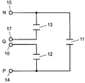
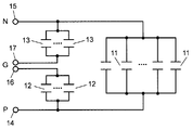
- the P pole 12A of the second element 12 is joined to the right end of the first main bus bar 14 joined to the P pole 11A of the first element 11.
- the N pole 13B of the third element 13 is joined to the right end of the second main bus bar 15 joined to the N pole 11B of the first element 11. In this way, the circuit shown in FIG. 5A is configured.
- a smoothing capacitor is applied as the first element 11, and a noise removing capacitor is applied as the second element 12 and the third element 13.
- the present invention is not limited to this. You may combine the capacitor
- the elements 11 to 13 have been described as metallized film capacitors, other types of capacitors may be used.
- electronic components other than capacitors may be embedded in the mold resin 19.
Abstract
Description
11A P極(第1電極)
11B N極(第2電極)
12 第2コンデンサ素子(第2素子)
12A P極(第3電極)
12B グランド電極(第4電極)
13 第3コンデンサ素子(第3素子)
13A グランド電極(第6電極)
13B N極(第5電極)
14 第1主バスバー
14A 端子部
15 第2主バスバー
15A 端子部
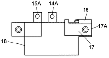
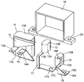
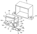
16 第1副バスバー
16A 取付穴
16B 第1端
16C 第2端
17 第2副バスバー
17A 取付穴
17B 第3端
17C 第4端
18 ケース
19 モールド樹脂
20 取付脚(取付部)
21 被装着体
22 ねじ
23 取付面
23A 切欠部 11 First capacitor element (first element)
11A P pole (first electrode)
11B N pole (second electrode)
12 Second capacitor element (second element)
12A P pole (third electrode)
12B Ground electrode (4th electrode)
13 Third capacitor element (third element)
13A Ground electrode (6th electrode)
13B N pole (5th electrode)
14 first
21
Claims (8)
- 第1電極と第2電極を有する第1コンデンサ素子と、
前記第1コンデンサ素子と機能が異なり、第3電極と第4電極を有する第2コンデンサ素子と、
前記第2コンデンサ素子と機能が同じで、第5電極と第6電極を有する第3コンデンサ素子と、
前記第1コンデンサ素子の前記第1電極と前記第2コンデンサ素子の前記第3電極とを接続する第1主バスバーと、
前記第1コンデンサ素子の前記第2電極と前記第3コンデンサ素子の前記第5電極とを接続する第2主バスバーと、
第1端と第2端を有し、前記第1端で前記第2コンデンサ素子の前記第4電極に接続された第1副バスバーと、
第3端と第4端を有し、前記第3端で前記第3コンデンサ素子の前記第6電極に接続された第2副バスバーと、
前記第1コンデンサ素子と前記第2コンデンサ素子と前記第3コンデンサ素子を収容するケースと、
前記第1主バスバーと前記第2主バスバーのそれぞれの一部が露出するように、かつ前記第1副バスバーの前記第2端と前記第2副バスバーの前記第4端が露出するように前記第1コンデンサ素子と前記第2コンデンサ素子と前記第3コンデンサ素子を埋設したモールド樹脂と、を備え、
前記第1副バスバーの前記第2端と前記第2副バスバーの前記第4端とが前記モールド樹脂の外で重なっている、
ケースモールド型コンデンサ。 A first capacitor element having a first electrode and a second electrode;
A second capacitor element having a function different from that of the first capacitor element and having a third electrode and a fourth electrode;
A third capacitor element having the same function as the second capacitor element and having a fifth electrode and a sixth electrode;
A first main bus bar connecting the first electrode of the first capacitor element and the third electrode of the second capacitor element;
A second main bus bar connecting the second electrode of the first capacitor element and the fifth electrode of the third capacitor element;
A first sub-bus bar having a first end and a second end and connected to the fourth electrode of the second capacitor element at the first end;
A second sub-bus bar having a third end and a fourth end and connected to the sixth electrode of the third capacitor element at the third end;
A case for housing the first capacitor element, the second capacitor element, and the third capacitor element;
The first main bus bar and the second main bus bar are partially exposed, and the second end of the first sub bus bar and the fourth end of the second sub bus bar are exposed. A mold resin in which the first capacitor element, the second capacitor element, and the third capacitor element are embedded;
The second end of the first sub bus bar and the fourth end of the second sub bus bar overlap outside the mold resin;
Case mold type capacitor. - 前記第1副バスバーの前記第2端と前記第2副バスバーの前記第4端には、前記ケースモールド型コンデンサを被装着体に電気的に結合するための結合部がそれぞれ設けられた、
請求項1記載のケースモールド型コンデンサ。 The second end of the first sub bus bar and the fourth end of the second sub bus bar are provided with coupling portions for electrically coupling the case mold type capacitor to the mounted body, respectively.
The case mold type capacitor according to claim 1. - 前記ケースは、前記ケースモールド型コンデンサを前記被装着体に結合するための取付部を有し、前記取付部は前記被装着体への取付面を有し、前記第1副バスバーと前記第2副バスバーにそれぞれ設けられた前記結合部が前記取付面に重なり合って配設された、
請求項2記載のケースモールド型コンデンサ。 The case has a mounting portion for coupling the case mold type capacitor to the mounted body, the mounting portion has a mounting surface to the mounted body, and the first sub-bus bar and the second The coupling portions provided on the sub bus bars are disposed so as to overlap the mounting surface,
The case mold type capacitor according to claim 2. - 前記被装着体への前記取付面に、前記第1副バスバーの前記第2端と前記第2副バスバーの前記第4端とが嵌まり込む切欠部が設けられた、
請求項3記載のケースモールド型コンデンサ。 A notch portion into which the second end of the first sub bus bar and the fourth end of the second sub bus bar are fitted is provided on the mounting surface to the mounted body.
The case mold type capacitor according to claim 3. - 前記第1コンデンサ素子は、互いに並列接続された複数のコンデンサ素子で構成されている、
請求項1記載のケースモールド型コンデンサ。 The first capacitor element is composed of a plurality of capacitor elements connected in parallel to each other.
The case mold type capacitor according to claim 1. - 前記第2コンデンサ素子が、互いに並列接続された複数のコンデンサ素子で構成されているか、
前記第3コンデンサ素子が、互いに並列接続された複数のコンデンサ素子で構成されているか、の少なくともいずれかである、
請求項1記載のケースモールド型コンデンサ。 Whether the second capacitor element is composed of a plurality of capacitor elements connected in parallel;
The third capacitor element is composed of a plurality of capacitor elements connected in parallel to each other, or at least one of them.
The case mold type capacitor according to claim 1. - 前記第1副バスバーの前記第2端と前記第2副バスバーの前記第4端は接地されており、
前記第2コンデンサと前記第3コンデンサはそれぞれ前記第2端と前記第4端からノイズを除去する除去用コンデンサである、
請求項1記載のケースモールド型コンデンサ。 The second end of the first sub bus bar and the fourth end of the second sub bus bar are grounded;
The second capacitor and the third capacitor are removal capacitors for removing noise from the second end and the fourth end, respectively.
The case mold type capacitor according to claim 1. - 前記第1コンデンサ素子が平滑用コンデンサである、
請求項7記載のケースモールド型コンデンサ。 The first capacitor element is a smoothing capacitor;
The case mold type capacitor according to claim 7.
Priority Applications (3)
| Application Number | Priority Date | Filing Date | Title |
|---|---|---|---|
| EP09831622.7A EP2352156A4 (en) | 2008-12-10 | 2009-11-11 | Case mold type capacitor |
| KR1020117013211A KR101310505B1 (en) | 2008-12-10 | 2009-11-11 | Case mold type capacitor |
| JP2010541975A JPWO2010067514A1 (en) | 2008-12-10 | 2009-11-11 | Case mold type capacitor |
Applications Claiming Priority (2)
| Application Number | Priority Date | Filing Date | Title |
|---|---|---|---|
| JP2008314039 | 2008-12-10 | ||
| JP2008-314039 | 2008-12-10 |
Publications (1)
| Publication Number | Publication Date |
|---|---|
| WO2010067514A1 true WO2010067514A1 (en) | 2010-06-17 |
Family
ID=42242512
Family Applications (1)
| Application Number | Title | Priority Date | Filing Date |
|---|---|---|---|
| PCT/JP2009/006002 WO2010067514A1 (en) | 2008-12-10 | 2009-11-11 | Case mold type capacitor |
Country Status (4)
| Country | Link |
|---|---|
| EP (1) | EP2352156A4 (en) |
| JP (1) | JPWO2010067514A1 (en) |
| KR (1) | KR101310505B1 (en) |
| WO (1) | WO2010067514A1 (en) |
Cited By (11)
| Publication number | Priority date | Publication date | Assignee | Title |
|---|---|---|---|---|
| US20130222967A1 (en) * | 2011-01-21 | 2013-08-29 | Panasonic Corporation | Case mold type capacitor |
| JP2014121260A (en) * | 2012-12-17 | 2014-06-30 | Lsis Co Ltd | Dc link capacitor assembly |
| JP2014170882A (en) * | 2013-03-05 | 2014-09-18 | Shizuki Electric Co Inc | Capacitor |
| JP2016139778A (en) * | 2015-01-22 | 2016-08-04 | カルソニックカンセイ株式会社 | Capacitor structure |
| JP2017050335A (en) * | 2015-08-31 | 2017-03-09 | 株式会社指月電機製作所 | Snubber module |
| JP2018500756A (en) * | 2014-11-28 | 2018-01-11 | ビーワイディー カンパニー リミテッドByd Company Limited | Film capacitor |
| US10079098B2 (en) * | 2012-12-10 | 2018-09-18 | Panasonic Intellectual Property Management Co., Ltd. | Case-mold-type capacitor and method for producing same |
| JP2019004120A (en) * | 2017-06-20 | 2019-01-10 | 株式会社指月電機製作所 | Capacitor and inspection method of the same |
| JPWO2018016349A1 (en) * | 2016-07-21 | 2019-05-16 | パナソニックIpマネジメント株式会社 | Capacitor |
| JP2020119919A (en) * | 2019-01-18 | 2020-08-06 | 株式会社Soken | Capacitor module |
| WO2023002831A1 (en) | 2021-07-19 | 2023-01-26 | ニチコン株式会社 | Composite capacitor |
Families Citing this family (2)
| Publication number | Priority date | Publication date | Assignee | Title |
|---|---|---|---|---|
| DE102013203614A1 (en) * | 2013-03-04 | 2014-08-07 | Siemens Aktiengesellschaft | Capacitor unit for use in intermediate circuit of frequency converter of e.g. electric vehicle, has screening and power capacitor arranged in housing, where terminals of screening capacitors are grounded over conducting part of housing |
| DE102019120334A1 (en) * | 2019-07-26 | 2021-01-28 | Jheeco E-Drive Ag | Capacitor housing and intermediate circuit capacitor with such a housing |
Citations (6)
| Publication number | Priority date | Publication date | Assignee | Title |
|---|---|---|---|---|
| JPS543345U (en) * | 1977-06-10 | 1979-01-10 | ||
| JPH1080040A (en) * | 1996-09-02 | 1998-03-24 | Yazaki Corp | Grounding structure of electrical connection box |
| JP2004040945A (en) * | 2002-07-05 | 2004-02-05 | Sumitomo Wiring Syst Ltd | Electronic control unit and its manufacturing method |
| JP2004146724A (en) | 2002-10-28 | 2004-05-20 | Matsushita Electric Ind Co Ltd | Metallized film capacitor |
| JP2007012769A (en) * | 2005-06-29 | 2007-01-18 | Honda Motor Co Ltd | Capacitor for inverter and composite capacitor |
| JP2009194281A (en) * | 2008-02-18 | 2009-08-27 | Panasonic Corp | Case-molded capacitor |
Family Cites Families (2)
| Publication number | Priority date | Publication date | Assignee | Title |
|---|---|---|---|---|
| FR2306597A1 (en) * | 1975-04-04 | 1976-10-29 | Embasaygues Marc | Electrical interference reduction capacitor - has fixture to connect conductors to adjacent circuit with hook and slot |
| JP4983217B2 (en) * | 2006-11-17 | 2012-07-25 | パナソニック株式会社 | Case mold type capacitor |
-
2009
- 2009-11-11 WO PCT/JP2009/006002 patent/WO2010067514A1/en active Application Filing
- 2009-11-11 EP EP09831622.7A patent/EP2352156A4/en not_active Withdrawn
- 2009-11-11 KR KR1020117013211A patent/KR101310505B1/en active IP Right Grant
- 2009-11-11 JP JP2010541975A patent/JPWO2010067514A1/en active Pending
Patent Citations (6)
| Publication number | Priority date | Publication date | Assignee | Title |
|---|---|---|---|---|
| JPS543345U (en) * | 1977-06-10 | 1979-01-10 | ||
| JPH1080040A (en) * | 1996-09-02 | 1998-03-24 | Yazaki Corp | Grounding structure of electrical connection box |
| JP2004040945A (en) * | 2002-07-05 | 2004-02-05 | Sumitomo Wiring Syst Ltd | Electronic control unit and its manufacturing method |
| JP2004146724A (en) | 2002-10-28 | 2004-05-20 | Matsushita Electric Ind Co Ltd | Metallized film capacitor |
| JP2007012769A (en) * | 2005-06-29 | 2007-01-18 | Honda Motor Co Ltd | Capacitor for inverter and composite capacitor |
| JP2009194281A (en) * | 2008-02-18 | 2009-08-27 | Panasonic Corp | Case-molded capacitor |
Non-Patent Citations (1)
| Title |
|---|
| See also references of EP2352156A4 * |
Cited By (16)
| Publication number | Priority date | Publication date | Assignee | Title |
|---|---|---|---|---|
| US8670223B2 (en) * | 2011-01-21 | 2014-03-11 | Panasonic Corporation | Case mold type capacitor |
| US20130222967A1 (en) * | 2011-01-21 | 2013-08-29 | Panasonic Corporation | Case mold type capacitor |
| US10079098B2 (en) * | 2012-12-10 | 2018-09-18 | Panasonic Intellectual Property Management Co., Ltd. | Case-mold-type capacitor and method for producing same |
| JP2014121260A (en) * | 2012-12-17 | 2014-06-30 | Lsis Co Ltd | Dc link capacitor assembly |
| US9107319B2 (en) | 2012-12-17 | 2015-08-11 | Lsis Co., Ltd. | DC link capacitor assembly |
| JP2014170882A (en) * | 2013-03-05 | 2014-09-18 | Shizuki Electric Co Inc | Capacitor |
| JP2018500756A (en) * | 2014-11-28 | 2018-01-11 | ビーワイディー カンパニー リミテッドByd Company Limited | Film capacitor |
| US10062515B2 (en) | 2015-01-22 | 2018-08-28 | Calsonic Kansei Corporation | Capacitor structure |
| JP2016139778A (en) * | 2015-01-22 | 2016-08-04 | カルソニックカンセイ株式会社 | Capacitor structure |
| JP2017050335A (en) * | 2015-08-31 | 2017-03-09 | 株式会社指月電機製作所 | Snubber module |
| JPWO2018016349A1 (en) * | 2016-07-21 | 2019-05-16 | パナソニックIpマネジメント株式会社 | Capacitor |
| JP7050229B2 (en) | 2016-07-21 | 2022-04-08 | パナソニックIpマネジメント株式会社 | Capacitor |
| JP2019004120A (en) * | 2017-06-20 | 2019-01-10 | 株式会社指月電機製作所 | Capacitor and inspection method of the same |
| JP2020119919A (en) * | 2019-01-18 | 2020-08-06 | 株式会社Soken | Capacitor module |
| JP7211827B2 (en) | 2019-01-18 | 2023-01-24 | 株式会社Soken | capacitor module |
| WO2023002831A1 (en) | 2021-07-19 | 2023-01-26 | ニチコン株式会社 | Composite capacitor |
Also Published As
| Publication number | Publication date |
|---|---|
| EP2352156A4 (en) | 2014-11-26 |
| KR20110082627A (en) | 2011-07-19 |
| KR101310505B1 (en) | 2013-09-25 |
| EP2352156A1 (en) | 2011-08-03 |
| JPWO2010067514A1 (en) | 2012-05-17 |
Similar Documents
| Publication | Publication Date | Title |
|---|---|---|
| WO2010067514A1 (en) | Case mold type capacitor | |
| WO2006109732A1 (en) | Metalized film capacitor, case module type capacitor using the same, inverter circuit, and vehicle drive motor drive circuit | |
| US7660099B2 (en) | Case molded capacitor | |
| KR100964043B1 (en) | Electronic component | |
| JP4001730B2 (en) | Power supply | |
| CN109997248B (en) | Connecting device for electrically connecting an electrical energy storage unit | |
| US20050168911A1 (en) | Capacitor module and capacitor battery comprising the same | |
| WO2012098622A1 (en) | Case mold type capacitor | |
| WO2009050829A1 (en) | Wiring board and its manufacturing method | |
| US9236189B2 (en) | Direct current capacitor module | |
| JP2010225970A (en) | Case mold type capacitor | |
| JP5012140B2 (en) | Case mold type capacitor and inspection method thereof | |
| JP5125582B2 (en) | Case mold type capacitor | |
| JP5484268B2 (en) | Capacitor | |
| JP2008130641A (en) | Case mold type capacitor | |
| JP4983540B2 (en) | Case mold type capacitor | |
| JP2015095627A (en) | Case mold type capacitor and manufacturing method thereof | |
| JP5328588B2 (en) | Capacitor | |
| JP2009088913A (en) | Noise filter | |
| JP2005108957A (en) | Case-mold film capacitor | |
| JP2006049070A (en) | Connector member | |
| JP5945684B2 (en) | Case mold type capacitor | |
| JP2009200378A (en) | Composite metallized-film capacitor | |
| US20200365324A1 (en) | Capacitor | |
| JP5228581B2 (en) | Case mold type capacitor |
Legal Events
| Date | Code | Title | Description |
|---|---|---|---|
| 121 | Ep: the epo has been informed by wipo that ep was designated in this application |
Ref document number: 09831622 Country of ref document: EP Kind code of ref document: A1 |
|
| ENP | Entry into the national phase |
Ref document number: 2010541975 Country of ref document: JP Kind code of ref document: A |
|
| WWE | Wipo information: entry into national phase |
Ref document number: 2009831622 Country of ref document: EP |
|
| ENP | Entry into the national phase |
Ref document number: 20117013211 Country of ref document: KR Kind code of ref document: A |
|
| NENP | Non-entry into the national phase |
Ref country code: DE |