WO2010061898A1 - 有機電界発光素子、表示装置および照明装置 - Google Patents
有機電界発光素子、表示装置および照明装置 Download PDFInfo
- Publication number
- WO2010061898A1 WO2010061898A1 PCT/JP2009/069975 JP2009069975W WO2010061898A1 WO 2010061898 A1 WO2010061898 A1 WO 2010061898A1 JP 2009069975 W JP2009069975 W JP 2009069975W WO 2010061898 A1 WO2010061898 A1 WO 2010061898A1
- Authority
- WO
- WIPO (PCT)
- Prior art keywords
- organic electroluminescent
- electroluminescent element
- shape
- layer
- light
- Prior art date
- Legal status (The legal status is an assumption and is not a legal conclusion. Google has not performed a legal analysis and makes no representation as to the accuracy of the status listed.)
- Ceased
Links
Images



Classifications
-
- H—ELECTRICITY
- H10—SEMICONDUCTOR DEVICES; ELECTRIC SOLID-STATE DEVICES NOT OTHERWISE PROVIDED FOR
- H10K—ORGANIC ELECTRIC SOLID-STATE DEVICES
- H10K50/00—Organic light-emitting devices
- H10K50/80—Constructional details
-
- H—ELECTRICITY
- H10—SEMICONDUCTOR DEVICES; ELECTRIC SOLID-STATE DEVICES NOT OTHERWISE PROVIDED FOR
- H10K—ORGANIC ELECTRIC SOLID-STATE DEVICES
- H10K50/00—Organic light-emitting devices
- H10K50/10—OLEDs or polymer light-emitting diodes [PLED]
-
- H—ELECTRICITY
- H10—SEMICONDUCTOR DEVICES; ELECTRIC SOLID-STATE DEVICES NOT OTHERWISE PROVIDED FOR
- H10K—ORGANIC ELECTRIC SOLID-STATE DEVICES
- H10K59/00—Integrated devices, or assemblies of multiple devices, comprising at least one organic light-emitting element covered by group H10K50/00
- H10K59/80—Constructional details
- H10K59/875—Arrangements for extracting light from the devices
-
- H—ELECTRICITY
- H10—SEMICONDUCTOR DEVICES; ELECTRIC SOLID-STATE DEVICES NOT OTHERWISE PROVIDED FOR
- H10K—ORGANIC ELECTRIC SOLID-STATE DEVICES
- H10K2101/00—Properties of the organic materials covered by group H10K85/00
- H10K2101/10—Triplet emission
-
- H—ELECTRICITY
- H10—SEMICONDUCTOR DEVICES; ELECTRIC SOLID-STATE DEVICES NOT OTHERWISE PROVIDED FOR
- H10K—ORGANIC ELECTRIC SOLID-STATE DEVICES
- H10K2102/00—Constructional details relating to the organic devices covered by this subclass
- H10K2102/301—Details of OLEDs
- H10K2102/302—Details of OLEDs of OLED structures
- H10K2102/3023—Direction of light emission
- H10K2102/3031—Two-side emission, e.g. transparent OLEDs [TOLED]
-
- H—ELECTRICITY
- H10—SEMICONDUCTOR DEVICES; ELECTRIC SOLID-STATE DEVICES NOT OTHERWISE PROVIDED FOR
- H10K—ORGANIC ELECTRIC SOLID-STATE DEVICES
- H10K50/00—Organic light-emitting devices
- H10K50/10—OLEDs or polymer light-emitting diodes [PLED]
- H10K50/11—OLEDs or polymer light-emitting diodes [PLED] characterised by the electroluminescent [EL] layers
Definitions
- the present invention relates to, for example, an organic electroluminescent element used for a display device or a lighting device.
- an organic electroluminescent element that emits light by forming a light emitting material made of an organic material in a layer and providing a pair of electrodes consisting of an anode and a cathode on the light emitting layer and applying a voltage. It attracts attention.
- An organic electroluminescent element is produced by injecting holes and electrons from the anode and the cathode, respectively, by applying a voltage between the anode and the cathode, and the injected electrons and holes are combined in the light emitting layer. Uses energy to emit light. That is, the organic electroluminescent element is a device that utilizes a phenomenon in which light is generated when the light emitting material of the light emitting layer is excited by the energy of the coupling and returns from the excited state to the ground state again.
- this organic electroluminescent element When this organic electroluminescent element is used as a display device, since an organic substance is used as a light-emitting material, it is easy to generate light with high color purity by selecting an organic substance, and thus a wide color reproduction range can be obtained. There is the feature that it is. In addition, since the organic electroluminescent element is self-luminous, it has characteristics that a response speed is high and a viewing angle is wide when used as a display device. In addition, there is an advantage that it is easy to make the display device thinner due to the structure of the organic electroluminescent element. Furthermore, since the organic electroluminescent element can emit white light and is surface emitting, an application in which the organic electroluminescent element is incorporated in a lighting apparatus has been proposed.
- Patent Document 1 includes a dielectric layer inserted between a hole electrode injection layer and an electron injection electrode layer, and at least the dielectric layer and the electrode layer Cavity light emitting electroluminescent devices have been proposed that extend through one and apply an electroluminescent coating material to an internal cavity surface comprising a hole injection electrode region, an electron injection electrode region, and a dielectric region.
- the cavity light emitting electroluminescent device as described in JP-A-2003-522371 emits light only at the place where the cavity is manufactured, the area of the light emitting surface is effectively used. I can't say that.
- charge concentration tends to occur inside the cavity, there is a limit to increase the emission intensity by flowing a large current.
- an object of the present invention is to provide an organic electroluminescence device that is less likely to cause charge concentration in a light emitting portion and can effectively use the area of a light emitting surface. Another object is to provide a display device having high contrast and resolution and high luminous efficiency. Furthermore, another object is to provide a lighting device having high luminous efficiency.
- the organic electroluminescent element of the present invention comprises a first electrode layer, a second electrode layer, a dielectric layer formed between the first electrode layer and the second electrode layer, and at least a dielectric layer.
- a concave portion formed through and a light emitting portion that is formed in contact with the inner surface of the concave portion and emits light by supplying an electric current, and the circumferential length of the shape viewed from the light extraction side of the concave portion, It is characterized by being longer than the circumference of the smallest circle containing the shape.
- the shape is preferably a concave polygonal shape, and the concave polygonal shape further preferably has 8 or more vertices.
- the shape is preferably a shape having a fractal structure. And it is preferable that the length of the side which comprises a shape is substantially the same, and it is still more preferable to set it as the shape which further chamfers the vertex part of a shape.
- the display device of the present invention includes the organic electroluminescent element described above.
- the lighting device of the present invention is characterized by including the organic electroluminescent element described above.
- an organic electroluminescent element or the like that is less likely to cause charge concentration in the light emitting portion and can effectively use the area of the light emitting surface.
- (A)-(c) is a figure explaining the case where a concave decagon was chamfered by two methods.
- (A)-(d) is a figure explaining the other form of the shape of the light emission part.
- (A)-(f) is the figure explaining the various forms of the recessed part of an organic electroluminescent element.
- (A)-(f) is a figure explaining the manufacturing method of the organic electroluminescent element to which this Embodiment is applied. It is a figure explaining an example of a display apparatus provided with the organic electroluminescent element in this Embodiment. It is a figure explaining an example of an illuminating device provided with the organic electroluminescent element in this Embodiment.
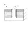
- FIG. 1 is a partial cross-sectional view illustrating an example of an organic electroluminescent element to which the exemplary embodiment is applied.
- the organic electroluminescent device 10 shown in FIG. 1 is for injecting electrons onto a substrate 11 as an anode layer 12 as a first electrode layer for injecting holes, an insulating dielectric layer 13, and electrons.
- the cathode layer 14 as the second electrode layer is sequentially stacked.
- a recess 16 formed through the anode layer 12, the dielectric layer 13, and the cathode layer 14, and is made of a light emitting material that is formed in contact with the inner surface of the recess 16 and emits light when a voltage is applied.
- a light emitting unit 17 is included. In the light emitting portion 17, a light emitting material is applied to the inner surface of the recessed portion 16 without filling the entire recessed portion 16, thereby forming a second recessed portion 18.
- the substrate 11 serves as a support for forming the anode layer 12, the dielectric layer 13, the cathode layer 14, and the light emitting portion 17.
- a material that satisfies the mechanical strength required for the organic electroluminescent element 10 is used for the substrate 11.
- glass such as soda glass and non-alkali glass
- transparent plastic such as acrylic resin, methacrylic resin, polycarbonate resin, polyester resin and nylon resin
- silicon resin and the like are examples of the like.
- the material of the substrate 11 is not limited to a material transparent to visible light, and an opaque material can be used. Specifically, in addition to the above materials, silicon (Si), copper (Cu), silver (Ag), gold (Au), platinum (Pt), tungsten (W), titanium (Ti), tantalum (Ta) Alternatively, niobium (Nb) alone, alloys thereof, or materials made of stainless steel can also be used.
- the thickness of the substrate 11 is preferably 0.1 mm to 10 mm, more preferably 0.25 mm to 2 mm, although it depends on the required mechanical strength.
- the anode layer 12 applies voltage between the cathode layer 14 and injects holes into the light emitting portion 17.
- the material used for the anode layer 12 is not particularly limited as long as it has electrical conductivity, but preferably has a sheet resistance of 1000 ⁇ or less in a temperature range of ⁇ 5 ° C. to 80 ° C. More preferably, it is 100 ⁇ or less. In addition, it is preferable that the electrical resistance does not change significantly with respect to the alkaline aqueous solution.
- Metal oxides, metals, and alloys can be used as materials that satisfy such conditions.
- examples of the metal oxide include ITO (indium tin oxide) and IZO (indium-zinc oxide).
- the metal examples include stainless steel, copper (Cu), silver (Ag), gold (Au), platinum (Pt), tungsten (W), titanium (Ti), tantalum (Ta), niobium (Nb), and the like. .
- An alloy containing these metals can also be used.
- the anode layer 12 needs to be a transparent electrode when it is desired to extract light from the substrate 11 side of the organic electroluminescent element 10.
- the transparent material used to form the transparent electrode include indium oxide, zinc oxide, tin oxide, and conductive materials made of ITO (indium tin oxide), IZO (indium-zinc oxide), which are composites thereof. Glass (NESA etc.), gold, platinum, silver and copper.
- ITO, IZO, and tin oxide are preferable.
- a transparent conductive film made of an organic material such as polyaniline or a derivative thereof, polythiophene or a derivative thereof may be used.
- a conductive polymer such as a phthalocyanine derivative and a polythiophene derivative, Mo oxide, amorphous on the surface of the anode layer 12 in contact with the light emitting portion 17
- a layer having a thickness of 1 nm to 200 nm made of carbon, carbon fluoride, polyamine compound, or the like, or a layer having an average film thickness of 10 nm or less made of metal oxide, metal fluoride, organic insulating material, or the like may be provided.
- the thickness of the anode layer 12 is preferably 2 nm to 300 nm because high light transmittance is required when light is to be extracted from the substrate 11 side of the organic electroluminescent element 10. Further, when it is not necessary to extract light from the substrate 11 side of the organic electroluminescent element 10, it can be formed with a thickness of 2 nm to 2 mm, for example.
- the anode layer 12 may be made of the same material as the substrate 11. In this case, the anode layer 12 and the substrate 11 are integrated.
- the dielectric layer 13 is formed between the anode layer 12 and the cathode layer 14, and separates and insulates the anode layer 12 and the cathode layer 14 at a predetermined interval, and applies a voltage to the light emitting unit 17. It is. Therefore, the dielectric layer 13 needs to be a high resistivity material, and the resistivity is required to be 10 8 ⁇ ⁇ cm or more, preferably 10 12 ⁇ ⁇ cm or more. Specific examples of the material include metal nitrides such as silicon nitride, boron nitride, and aluminum nitride; metal oxides such as silicon oxide and aluminum oxide, but other polymer compounds such as polyimide, polyvinylidene fluoride, and parylene. Can also be used.
- the dielectric layer 13 may be composed of two or more layers as long as electrical insulation is maintained. Specifically, in addition to a layer made of an insulator, a layer made of an insulator, a layer made of a conductor, a layer in which a conductor is dispersed in an insulator, a layer in which an insulator is dispersed in an insulator, a semiconductor A layer made of or the like may be laminated.
- the material used for the additional layer is not particularly limited, and specifically, metal nitrides such as silicon nitride, boron nitride, and aluminum nitride; silicon oxide, aluminum oxide, indium oxide, zinc oxide, tin oxide, and the like Composite metal oxides such as ITO (indium tin oxide) and IZO (indium-zinc oxide); stainless steel, copper (Cu), silver (Ag), gold (Au), platinum (Pt), tungsten (W ), Titanium (Ti), tantalum (Ta), niobium (Nb) and other metals; conductive polymers, organic conductive materials such as organic EL light-emitting materials; graphite, alumina, boron nitride, carbon nanotubes, powder diamond, powder silicon Or the like dispersed in an insulator such as a resin.
- metal nitrides such as silicon nitride, boron nitride, and aluminum nitride
- the thickness of the dielectric layer 13 is preferably not more than 1 ⁇ m in order to suppress the total thickness of the organic electroluminescent element 10. Also, the narrower the gap between the anode layer 12 and the cathode layer 14, the lower the voltage required for light emission. From this point of view, the thinner the dielectric layer 14 is more preferable. However, if the thickness is too thin, the dielectric strength may not be sufficient for the voltage for driving the organic electroluminescent element 10.
- the dielectric strength is preferably such that the current density of the current flowing between the anode layer 12 and the cathode layer 14 is 0.1 mA / cm 2 or less when the light emitting portion 17 is not formed, and 0.01 mA. / Cm 2 or less is more preferable.
- the anode layer 12 and the anode layer 12 are not formed in a state where the light emitting portion 17 is not formed. It is necessary to satisfy the above current density when a voltage of about 7 V is applied between the cathode layers 14.
- the thickness of the dielectric layer 13 satisfying this is preferably 10 nm to 500 nm, more preferably 50 nm to 200 nm.
- the cathode layer 14 applies a voltage between the anode layer 12 and injects electrons into the light emitting portion 17.
- the material used for the cathode layer 14 is not particularly limited as long as it has electrical conductivity like the anode layer 12, but a material having a low work function and being chemically stable is preferable. .
- the work function is preferably ⁇ 2.9 eV or less in view of chemical stability. Specifically, materials such as Al, MgAg alloy, Al and alkali metal alloys such as AlLi and AlCa can be exemplified.
- the thickness of the cathode layer 14 is preferably 10 nm to 1 ⁇ m, more preferably 50 nm to 500 nm.
- a cathode buffer layer may be provided adjacent to the cathode layer 14 for the purpose of lowering the electron injection barrier from the cathode layer 14 to the light emitting portion 17 and increasing the electron injection efficiency.
- the cathode buffer layer needs to have a lower work function than the cathode layer 14, and a metal material is preferably used.
- a metal material is preferably used.
- alkali metals Na, K, Rb, Cs
- alkaline earth metals Sr, Ba, Ca, Mg
- rare earth metals Pr, Sm, Eu, Yb
- fluorides or chlorides of these metals A simple substance selected from oxides or a mixture of two or more can be used.
- the thickness of the cathode buffer layer is preferably from 0.05 nm to 50 nm, more preferably from 0.1 nm to 20 nm, and even more preferably from 0.5 nm to 10 nm.
- the concave portion 16 is for applying the light emitting portion 17 on the inner surface and taking out light from the light emitting portion 17.
- the anode layer 12 and the dielectric layer 13 are the first electrode layers.
- the second electrode layer is formed so as to penetrate the cathode layer 14.
- the light emitted from the light emitting portion 17 by providing the concave portion 16 in this way propagates through the concave portion 16 and can be extracted in both directions on the substrate 11 side and the cathode layer 14 side.
- the recess 16 is formed through the anode layer 12, the dielectric layer 13, and the cathode layer 14, the anode layer 12 that is the first electrode layer and the cathode layer 14 that is the second electrode layer. It is possible to extract light even when is made of an opaque material.
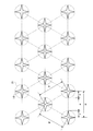
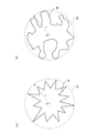
- FIG. 2 is a diagram illustrating the shape and arrangement of the recesses 16 of the organic electroluminescent element 10 to which the present exemplary embodiment is applied.
- FIG. 2 is a view of the organic electroluminescent element 10 as seen from the light extraction direction.
- the concave portion 16 takes a concave octagonal shape as will be described in detail later.
- the recesses 16 are arranged in three rows, and adjacent rows are arranged in a staggered manner. Then, considering the minimum circle 21 (minimum inclusion circle) that encloses the concave octagon, the line segments that connect the centers of the adjacent minimum circles 21 are arranged to form an equilateral triangle.
- minimum circle 21 minimum inclusion circle
- the “minimum inclusion circle” refers to the smallest one of the circles including all the shapes taken by the recesses 16 inside.
- the concave portion 16 has the shape of the minimum circle 21
- the light emitting portion 17 is formed in a circular shape along the outer edge of the circular shape as can be seen from FIG. Therefore, light emission occurs in a circular shape at the outer edge of the minimum circle 21. If the separation (s), which is the distance between each, is reduced, the number of recesses 16 per unit area increases accordingly, so that the emission intensity can be increased.
- the separation (s) which is the distance between each
- the circumferential length of the shape of the concave portion 16 viewed from the light extraction side is made longer than the circumferential length of the minimum circle 21 containing this shape.
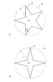
- 3A and 3B are diagrams illustrating the shape of the recess 16 in the organic electroluminescent element 10 of the present embodiment.
- the recess 16 shown in FIGS. 3A and 3B has a shape when viewed from the light extraction direction of the organic electroluminescent element 10.
- the recessed part 16 shown to Fig.3 (a) it is the shape similar to the recessed part 16 shown in FIG.
- the shape of the recess 16 is a concave octagon that is one of the concave polygonal shapes.
- the length of the side which comprises this concave octagon is substantially the same.
- the perimeter as the sum of the lengths of the sides is longer than the perimeter of the smallest circle 21 that encloses the concave octagon (that is, the length of the circumference).
- the shape of the recessed part 16 is a concave decagon which is one of the concave polygons, and is what is called a star shape.
- the apex angle at the apex of the concave decagonal projection is 36 °.
- the lengths of the sides constituting the concave decagon are substantially the same.
- the “concave polygon” is a polygon having an internal angle of 180 degrees or more.
- the concave polygon shape preferably has eight or more vertices. By having eight or more vertices, the circumference of the concave polygon tends to be longer than the circumference of the minimum circle 21 containing the concave polygon.
- the concave portion 16 By forming the concave portion 16 as shown in FIGS. 3A to 3B, the light emitting area in the concave portion 16 is increased as compared with the case where the concave portion 16 is simply formed into a circular shape. Therefore, when a constant current is passed through the organic electroluminescent element 10, the amount of current flowing in the unit light emitting area is reduced as compared with the circular shape. Therefore, the current density in the recess 16 can be lowered. When the current density is lowered, the current luminous efficiency, which is the luminous efficiency with respect to the current, can be increased, and the voltage applied to the organic electroluminescent element 10 can be lowered. As a result, it is possible to increase the light emission intensity without reducing the isolation (s) (see FIG.
- the lengths of the sides are substantially the same, it is possible to further suppress the charge concentration to a specific portion.
- the fact that the lengths of the sides are substantially the same does not mean that they are the same length in a strict sense, but means that the lengths may be approximately the same.
- an index called “edge density” is used to compare the circumference of the shape of the concave portion 16 as viewed from the light extraction side with the circumference of the minimum circle 21 containing this shape. it can.
- This edge density represents the length of the edge of the recess 16 per unit area, that is, the circumference.
- the repeating unit of the arrangement of the recesses 16 is an equilateral triangle, so the circumference of the portion belonging to the equilateral triangle is first calculated. To do.
- the recess 16 has a circular shape, the circumference of this circle belonging to one corner portion of this equilateral triangle (that is, the circumference) is 1/6 of the circumference of the circle.
- the area of the equilateral triangle, than the length of one side is p, a ⁇ 3p 2/4. Therefore, the edge density, which is the length of the edge of the recess 16 per unit area, is 4 ⁇ 3 ⁇ r / (3p 2 ), which can be approximated to 7.26 r / p 2 .
- This edge density is calculated using the concave polygon shown in FIGS.
- the edge density in the case of the concave octagon shown in FIG. 3A, in the concave octagon when the length of one side is 4/5 of r, that is, 4r / 5, the edge density is 64 ⁇ 3r / ( 15p 2 ). This can be approximated as 7.39 r / p 2 .
- the edge density is 20 ⁇ 3 (3- ⁇ 5) rsin72 ° / (3p 2 ). This can be approximated as 8.39 r / p 2 . Therefore, since the edge density is higher than 7.26 r / p 2 in all cases, the circumference of the shape viewed from the light extraction side of the recess 16 is longer than the circumference of the minimum circle 21 containing this shape. .
- the shape of the concave portion 16 when viewed from the light extraction direction of the organic electroluminescent element 10 is a shape viewed from the light extraction side of the concave portion 16. Cannot be made longer than the circumference of the minimum circle 21 containing this shape.
- an equilateral triangle is considered as a convex polygon
- the edge density is 6r / p 2 where r is the radius of the smallest circle 21 containing the equilateral triangle.
- the edge density when a square is considered as the convex polygon is 8 ⁇ 6r / (3p 2 ). This can be approximated to 6.53 r / p 2 . Both are lower than 7.26 r / p 2 in the case of a circular shape. If the number of sides of the convex polygon is increased, the edge density approaches the edge density of the minimum circle 21 containing the convex polygon, but cannot be exceeded.
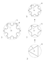
- FIG. 4A is a diagram illustrating another shape of the recess 16 in the organic electroluminescent element 10 of the present embodiment.
- the shape of the recess 16 shown in FIG. 4A is a shape having a fractal structure. This shape is a shape that appears in the middle when the three line segments constituting each side of the equilateral triangle are transformed into Koch curves.
- Figures 4 (b) to (d) show how to create this shape.
- the regular triangle is the starting shape (FIG. 4B).
- each of the three line segments constituting the side of the equilateral triangle is divided into three equal parts, and the equilateral triangle is plotted with the two divided points as apexes (FIG. 4C).
- the shape which consists of 12 sides is made.
- the lengths of these 12 sides are all the same, and the total length is 4/3 times the original equilateral triangle.
- FIG. 4D the same operation as that performed in FIG. 4B is further performed for all the 12 sides.
- FIG. 4A composed of 48 sides can be obtained.
- the shape created in this way is the original triangle of FIG. 4B, which is the original shape, the first generation, the shape of FIG. 4C is the second generation, and FIG. ) (FIG. 4A) is called the third generation.
- Each shape has a self-similarity that becomes the same shape as the whole when each portion of the shape is enlarged.
- the edge density when the radius of the minimum circle 21 containing this shape is r is calculated to be 8r / p 2 , which is the edge density of the minimum circle 21 7 .26 r / p 2 is exceeded.
- the edge density is 32r / (3p 2 ) when the radius of the minimum circle 21 containing this shape is defined as r. This can be approximated to 10.67 r / p 2 and the edge density can be further increased.
- the shapes having the fractal structure shown in FIGS. 4B to 4D have the regular triangle as the starting shape and the shapes of the second generation to the third generation, but are not limited thereto. .
- a square, regular pentagon, regular hexagon, or the like may be used as the starting shape.
- the generation preferable as the shape viewed from the light extraction side of the concave portion 16 is preferably a shape that can be created in the second to fourth generations from the viewpoint of ease of production of the concave portion 16.
- FIGS. 5A and 5B are views for explaining still another shape of the recess 16 in the organic electroluminescent element 10 of the present embodiment.
- the shape of the recess 16 shown in FIG. 5 (a) is a concave polygon, but the length of each side is not substantially the same, and takes various lengths. Even in such a shape, the circumference of the shape can be made longer than the circumference of the minimum circle 21 that encloses the shape.
- each shape is formed by a plurality of line segments.
- the shape is not limited to this, and may be configured by a curve.
- the shape of the recess 16 shown in FIG. 5B is an example of this case, and the shape of the recess 16 is configured by an irregular curve.
- the circumference of a shape is longer than the circumference of the minimum circle 21 containing this shape.
- the recess 16 shown in FIG. 6 shows another example in which the shape of the recess 16 is configured by a curve.
- the recess 16 has a substantially circular shape constituted by a curved line having regularity. Even in this case, the circumferential length of the shape of the concave portion 16 can be made longer than the circumferential length of the minimum circle 21 containing this shape.
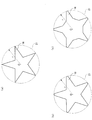
- FIGS. 7A to 7C are diagrams illustrating the case where the concave decagon is chamfered by two methods.
- FIG. 7B shows a case where each vertex of the concave decagon shown in FIG. By this chamfering, each vertex is gently rounded into an arc shape.
- FIG. 7C shows a case where each vertex of the concave decagon shown in FIG. 7A is chamfered. By this chamfering, each vertex is rounded into a straight line.
- the apex portion can be made gentler than before chamfering, charge concentration in this portion can be suppressed. In the example shown in FIGS.
- the chamfering is performed for all the vertex portions, but it is particularly preferable to perform the chamfering on the convex portion among the vertex portions.
- the convex portion has an acute angle, and charge concentration is likely to occur. By chamfering this portion, charge concentration can be more effectively suppressed.
- the light emitting portion 17 is a light emitting material that emits light when a voltage is applied. As described above, the light emitting portion 17 is applied to the inner surface of the recess 16 so as to form the second recess 18 by providing the light emitting material in contact with the recess 16. The In the light emitting unit 17, the holes injected from the anode layer 12 and the electrons injected from the cathode layer 15 are recombined to emit light.
- the material of the light emitting portion 17 either a low molecular compound or a high molecular compound can be used.
- a low molecular compound or a high molecular compound can be used as the material of the light emitting portion 17.
- the luminescent low molecular weight compound and the luminescent high molecular weight compound described in Hiroshi Omori: Applied Physics, Vol. 70, No. 12, pp. 1419-1425 (2001) can be exemplified.
- a material excellent in applicability is preferable. That is, in the structure of the organic electroluminescent element 10 in the present embodiment, in order for the light emitting portion 17 to emit light stably in the recess 16, the light emitting portion 17 is in uniform contact with the inner surface of the recess 16 and the film thickness is uniformly formed. It is preferable that the coverage is improved. If the light emitting portion 17 is formed without using a material having excellent coating properties, the light emitting portion 17 is not in contact with the entire recess 16 or the film thickness of the inner surface of the recess 16 is not uniform. For this reason, variations in the brightness of light emitted from the recess 16 are likely to occur.
- the coating method it is easy to embed ink containing a light-emitting material in the concave portion 16, and thus it is possible to form a film with improved coverage even on a surface having irregularities.
- materials having a weight average molecular weight of 1,000 to 2,000,000 are preferably used mainly for the purpose of improving coating properties.
- coating property improvement additives such as a leveling agent and a defoaming agent, can also be added, and binder resin with few charge trap ability can also be added.
- examples of the material having excellent coatability include, for example, an arylamine compound having a predetermined structure and a molecular weight of 1500 to 6000 as disclosed in JP-A-2007-86639, and JP-A 2000-034476.
- examples thereof include the predetermined polymeric fluorescent substances.
- a light-emitting polymer compound is preferable in terms of simplifying the manufacturing process of the organic electroluminescent element 10, and a phosphorescent compound is preferable in terms of high light emission efficiency. Therefore, a phosphorescent polymer compound is particularly preferable.
- the addition amount of the low molecular light emitting material is preferably 30 wt% or less.
- the light-emitting polymer compound can be classified into a conjugated light-emitting polymer compound and a non-conjugated light-emitting polymer compound, and among them, the non-conjugated light-emitting polymer compound is preferable.
- the light-emitting material used in this embodiment is particularly preferably a phosphorescent non-conjugated polymer compound (a light-emitting material that is both a phosphorescent polymer and a non-conjugated light-emitting polymer compound).
- the light emitting portion 17 in the organic electroluminescent device 10 of the present invention is preferably a phosphorescent polymer (in which a phosphorescent unit emitting phosphorescence and a carrier transporting unit transporting carriers are included in one molecule ( A phosphorescent material).
- the phosphorescent polymer can be obtained by copolymerizing a phosphorescent compound having a polymerizable substituent and a carrier transporting compound having a polymerizable substituent.
- the phosphorescent compound is a metal complex containing a metal element selected from iridium (Ir), platinum (Pt), and gold (Au), and among them, an iridium complex is preferable.
- Examples of the polymerizable substituent in the phosphorescent compound include a urethane (meth) acrylate group such as a vinyl group, an acrylate group, a methacrylate group, and a methacryloyloxyethyl carbamate group, a styryl group and a derivative thereof, a vinylamide group and a derivative thereof, and the like.
- a urethane (meth) acrylate group such as a vinyl group, an acrylate group, a methacrylate group, and a methacryloyloxyethyl carbamate group
- a styryl group and a derivative thereof a vinylamide group and a derivative thereof, and the like.
- vinyl group, methacrylate group, styryl group and derivatives thereof are preferable.
- These substituents may be bonded to the metal complex via an organic group having 1 to 20 carbon atoms which may have a hetero atom.
- a carrier transporting compound having a polymerizable substituent is a compound in which one or more hydrogen atoms in an organic compound having one or both of a hole transporting property and an electron transporting property are substituted with a polymerizable substituent. Can be mentioned.
- the polymerizable substituent in the carrier transporting compound is a vinyl group.
- the vinyl group is a urethane (meth) acrylate group such as an acrylate group, a methacrylate group, or a methacryloyloxyethyl carbamate group, a styryl group and a derivative thereof, a vinylamide group and a derivative thereof.
- a compound substituted with a polymerizable substituent such as may be used.
- These polymerizable substituents may be bonded via an organic group having 1 to 20 carbon atoms which may have a hetero atom.
- the polymerization method of the phosphorescent compound having a polymerizable substituent and the carrier transporting compound having a polymerizable substituent may be any of radical polymerization, cationic polymerization, anionic polymerization, and addition polymerization, but radical polymerization is preferred.
- the molecular weight of the polymer is preferably 1,000 to 2,000,000, more preferably 5,000 to 1,000,000 in terms of weight average molecular weight.
- the molecular weight here is a molecular weight in terms of polystyrene measured using a GPC (gel permeation chromatography) method.
- the phosphorescent polymer may be a copolymer of one phosphorescent compound and one carrier transporting compound, one phosphorescent compound and two or more carrier transporting compounds, or two.
- the above phosphorescent compound may be copolymerized with a carrier transporting compound.
- the arrangement of the monomer in the phosphorescent polymer may be any of random copolymer, block copolymer, and alternating copolymer, the number of repeating units of the phosphorescent compound structure is m, and the repeating unit of the carrier transporting compound structure
- the number is n (m, n is an integer of 1 or more)
- the ratio of the number of repeating units of the phosphorescent compound structure to the total number of repeating units, that is, the value of m / (m + n) is 0.001 to 0.00. 5 is preferable, and 0.001 to 0.2 is more preferable.
- JP-A Nos. 2003-342325, 2003-119179, 2003-113246, and 2003-206320 JP-A-2003-147021, JP-A-2003-171391, JP-A-2004-346212, JP-A-2005-97589, and JP-A-2007-305734.
- the light emitting portion 17 of the organic electroluminescent element 10 in the present embodiment preferably includes the above-described phosphorescent compound, but a hole transporting compound or an electron transporting compound is used for the purpose of supplementing the carrier transportability of the light emitting portion 17. It may be included.
- the hole transporting compound used for these purposes for example, TPD (N, N′-dimethyl-N, N ′-(3-methylphenyl) -1,1′-biphenyl-4,4′diamine) , ⁇ -NPD (4,4′-bis [N- (1-naphthyl) -N-phenylamino] biphenyl), m-MTDATA (4,4 ′, 4 ′′ -tris (3-methylphenylphenylamino) And low molecular triphenylamine derivatives such as triphenylamine).
- TPD N, N′-dimethyl-N, N ′-(3-methylphenyl) -1,1′-biphenyl-4,4′diamine
- ⁇ -NPD 4,4′-bis [N- (1-naphthyl) -N-phenylamino] biphenyl
- m-MTDATA (4,4 ′, 4 ′′ -tris (3-
- polyvinylcarbazole a triphenylamine derivative obtained by introducing a polymerizable functional group into a polymer; a polymer compound having a triphenylamine skeleton disclosed in JP-A-8-157575; polyparaphenylene vinylene, And polydialkylfluorene.
- the electron transporting compound include low molecular weight materials such as quinolinol derivative metal complexes such as Alq3 (aluminum triskinolinolate), oxadiazole derivatives, triazole derivatives, imidazole derivatives, triazine derivatives, and triarylborane derivatives.
- a polymer obtained by introducing a polymerizable functional group into the above low molecular electron transporting compound for example, a known electron transporting compound such as poly PBD disclosed in JP-A-10-1665 is exemplified. .
- the light emitting portion 17 can be formed even when a light emitting low molecular weight compound is used as the light emitting material used for the light emitting portion 17 instead of the light emitting polymer compound described above.
- the above-described light-emitting polymer compound can be added as a light-emitting material, and a hole-transporting compound or an electron-transporting compound can also be added.
- the hole transporting compound in this case include, for example, TPD, ⁇ -NPD, m-MTDATA, phthalocyanine complex, DTDPFL, spiro-TPD, TPAC, PDA described in JP-A-2006-76901. Etc.
- electron transport compound examples include BPhen, BCP, OXD-7, TAZ and the like described in JP-A-2006-76901.
- the light emitting portion 17 is in contact with the concave portion 16 to form the second concave portion 18 by providing the light emitting material, and although the bottom part of the 2nd recessed part 18 is formed so that it may be located in the location near the bottom part of the recessed part 16, it is not restricted to this.
- FIGS. 8A to 8D are diagrams for explaining other forms of the shape of the light-emitting portion 17.
- the depth of the second recess 18 is shallow, and the bottom of the second recess 18 is formed so as to be located closer to the top than the bottom of the recess 16. ing.
- the second recess 18 is not formed, and the recess 16 is entirely filled with the light emitting portion 17, and the upper surface of the light emitting portion 17 is the upper surface of the cathode layer 14. Is consistent with Furthermore, in the organic electroluminescent element 10c shown in FIG.
- the second concave portion 18 is not formed, the concave portion 16 is completely filled with the light emitting portion 17, and the upper surface thereof has a convex shape. Furthermore, in the organic electroluminescent element 10 d shown in FIG. 8D, the second recess 18 is formed, but the depth of the second recess 18 is shallow, and the bottom of the second recess 18 is the bottom of the recess 16. The light emitting part 17 is formed so as to be developed not only inside the concave part 16 but also on the upper surface of the cathode layer 14. Also in the organic electroluminescent elements 10a, 10b, 10c, and 10d shown in FIGS.
- the light emitted from the light emitting section 17 propagates through the light emitting section 17, and the above-described organic electroluminescent elements are used. 10, it can be taken out from both the substrate 11 side and the cathode layer 14 side.
- the shape of the light emitting portion 17 described in FIG. 1 and FIGS. 8A to 8D can be selected depending on the cross-sectional structures of the anode layer 12 and the cathode layer 14, for example.
- the cathode layer 14 is penetrated by the recess 16 and the upper portion is opened.
- the cathode layer 14 is formed after the light emitting unit 17 is formed. Therefore, it is preferable to form the second recess 18 small or not because the coverage is improved when the cathode layer 14 is formed.
- the recess 16 is formed so as to penetrate the anode layer 12, the dielectric layer 13, and the cathode layer 14. This is not a limitation. In order for the light emitting portion 17 to emit light, it is sufficient that at least the dielectric layer 13 penetrates through the concave portion 16, and the other layers may or may not penetrate.
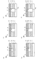
- FIGS. 9A to 9F are views for explaining various forms of the recess 16 of the organic electroluminescent element.
- the organic electroluminescent element 10 e shown in FIG. 9A is a case where the recess 16 penetrates the dielectric layer 13 but does not penetrate the anode layer 12 and the cathode layer 14.
- the light emitting material forming the light emitting portion 17 is formed so as to fill the concave portion 16. Therefore, the cathode layer 14 is formed in a planar shape on the upper surface of the dielectric layer 13 and the recess 16.
- the recess 16 penetrates the dielectric layer 13, but the organic electroluminescent element 10e is formed without penetrating the anode layer 12 and the cathode layer 14. It is the same.
- the light emitting material forming the light emitting portion 17 not only fills the concave portion 16 but also extends and expands on the upper surface of the dielectric layer 13 to form the extended portion 17a. Therefore, the cathode layer 14 is formed in a planar shape on the upper surfaces of the concave portion 16 and the extending portion 17a.
- the concave portion 16 penetrates the anode layer 12 and the dielectric layer 13, but does not penetrate the cathode layer. Also in the case of the organic electroluminescent device 10g, the light emitting material forming the light emitting portion 17 is formed so as to fill the concave portion 16 similarly to the organic electroluminescent device 10e, and the cathode layer 14 includes the dielectric layer 13 and the concave portion. 16 is formed in a planar shape on the upper surface.
- the organic electroluminescent element 10h shown in FIG.9 (d) is a case where the extending
- the concave portion 16 penetrates the anode layer 12 and the dielectric layer 13, but does not penetrate the cathode layer 14, similarly to the organic electroluminescent element 10g. is there.
- the recess 16 further includes a perforated portion 16 a formed by punching the substrate 11.
- the perforated portion 16a By forming the perforated portion 16a, the light emitted from the light emitting portion 17 can easily enter the substrate 11. As a result, the effect of improving the light extraction efficiency to the outside is produced.
- the organic electroluminescent element 10j shown in FIG.9 (f) is a case where the extending
- the concave portion 16 when the concave portion 16 does not penetrate the anode layer 12 or the cathode layer 14, and when it is desired to extract light in that direction, the anode layer 12 or The cathode layer 14 needs to be transparent to light in the emission wavelength region emitted from the light emitting unit 17.
- the anode layer 12 is the lower side.
- the case where the cathode layer 14 is formed on the upper side with the dielectric layer 13 interposed therebetween has been described by way of example.
- the present invention is not limited to this, and the anode layer 12 and the cathode layer 14 are interchanged. It may be a structure. That is, when the substrate 11 side is the lower side, the cathode layer 14 may be formed on the lower side, and the anode layer 12 may be formed on the upper side with the dielectric layer 13 interposed therebetween.
- FIG. 10A to 10F are diagrams illustrating a method for manufacturing the organic electroluminescent element 10 to which the exemplary embodiment is applied.
- An anode layer 12, a dielectric layer 13, and a cathode layer 14 are sequentially stacked on the substrate 11 (FIG. 10A).
- resistance heating vapor deposition, electron beam vapor deposition, sputtering, ion plating, CVD, or the like can be used.
- a coating film forming method that is, a method in which a target material is dissolved in a solvent and applied to a substrate and drying is possible
- a spin coating method a dip coating method, an ink jet method, a printing method, a spray method
- a method such as a dispenser method.
- the cathode buffer layer can also be formed by the same method.
- the performance of the overcoated layer (adhesion with the anode layer 12, surface smoothness, reduction of the hole injection barrier, etc.) can be improved.
- the surface treatment includes high-frequency plasma treatment, sputtering treatment, corona treatment, UV ozone irradiation treatment, ultraviolet irradiation treatment, oxygen plasma treatment, and the like.
- anode buffer layer (not shown) instead of or in addition to the surface treatment of the anode layer 12.
- anode buffer layer is applied by a wet process, spin coating, casting, micro gravure coating, gravure coating, bar coating, roll coating, wire bar coating, dip coating
- the film can be formed using a coating method such as a spray method, a spray coating method, a screen printing method, a flexographic printing method, an offset printing method, or an inkjet printing method.
- the compound that can be used in the film formation by the wet process is not particularly limited as long as the compound has good adhesion to the light-emitting compound contained in the anode layer 12 and the light-emitting portion 17.
- Examples thereof include conductive polymers such as PEDOT, which is a mixture of poly (3,4) -ethylenedioxythiophene and polystyrene sulfonate, and PANI, which is a mixture of polyaniline and polystyrene sulfonate.
- an organic solvent such as toluene or isopropyl alcohol may be added to these conductive polymers.
- the conductive polymer containing 3rd components, such as surfactant may be sufficient.
- the surfactant is, for example, selected from the group consisting of alkyl groups, alkylaryl groups, fluoroalkyl groups, alkylsiloxane groups, sulfates, sulfonates, carboxylates, amides, betaine structures, and quaternized ammonium groups.
- Surfactants containing one group are used, but fluoride-based nonionic surfactants can also be used.
- the anode buffer layer when the anode buffer layer is produced by a dry process, the anode buffer layer can be formed by using a plasma treatment or the like exemplified in Japanese Patent Application Laid-Open No. 2006-303412.
- a method of forming a film of a single metal, a metal oxide, a metal nitride, or the like can be given.
- Specific film forming methods include an electron beam evaporation method, a sputtering method, a chemical reaction method, a coating method, and a vacuum evaporation method. The method etc. can be used.
- the concave portion 16 is formed so as to penetrate each layer formed in the step of FIG. 10A.
- a method using lithography can be used. In order to do this, first, a resist solution is applied onto the cathode layer 14, and the excess resist solution is removed by spin coating or the like to form a resist layer 71 (FIG. 10B).
- a mask (not shown) on which a predetermined pattern for forming the recess 16 is drawn is placed, and exposure is performed with ultraviolet rays (UV: Ultra Violet), electron beams (EB), or the like.
- UV ultraviolet rays
- EB electron beams
- the mask pattern is a pattern in which openings having a shape corresponding to the shape of the recess 16 as described above are regularly arranged.
- a predetermined pattern 72 in which the shapes of the recesses 16 are regularly arranged on the resist layer 71 is exposed (FIG. 10C).
- the mask pattern and the pattern of the concave portion 16 have the same size as that of the mask pattern if the reduced exposure (for example, in the case of exposure using a stepper) is performed.
- the pattern of the recessed part 16 reduced with respect to the pattern can each be formed. Further, by performing exposure while intentionally shifting the focus of the exposure apparatus during exposure, the image of the mask projected on the resist layer can be blurred. By doing in this way, the chamfering of the pattern of the recessed part 16 can also be performed. That is, for example, the pattern of the recesses 16 in FIG. 7B or FIG. 7C can be formed by using a mask that originally has the pattern of the recesses 16 in FIG.
- the exposed portion of the cathode layer 14 is removed by etching, and a recess 16 is formed so as to penetrate each layer formed in the step of FIG. 10A (FIG. 10E).
- etching either dry etching or wet etching can be used.
- the shape of the recess 16 can be controlled by combining isotropic etching and anisotropic etching.
- dry etching reactive ion etching (RIE) or inductively coupled plasma etching can be used.
- RIE reactive ion etching
- wet etching a method of immersing in dilute hydrochloric acid or dilute sulfuric acid can be used.
- the recess 16 is formed in which the shape viewed from the light extraction side is the predetermined shape as described above.
- the layer through which the recess 16 penetrates can be selected by adjusting the etching conditions (processing time, gas used, pressure, substrate temperature). That is, the anode layer 12 can be left and the dielectric layer 13 and the cathode layer 14 can be penetrated. Further, after the anode layer 12 is removed, further etching can be performed to form the perforated portion 16a described with reference to FIGS. 9 (e) to 9 (f).
- the steps of FIG. 10B to FIG. 10D can also be performed by a nanoimprint method. Specifically, after forming the resist layer 71 as shown in FIG. 10B, a mask on which a predetermined convex pattern for forming the pattern 72 is drawn is pressed against the resist layer 71 with pressure. . In this state, the photoresist is cured by irradiating the resist surface with heat or / and light. Next, by removing the mask, a pattern 72 that is a pattern of the concave portions 16 corresponding to the convex patterns is formed on the photoresist surface. Subsequently, the recess 16 can be formed by performing the etching described above.
- the remaining resist layer 71 is removed using a resist removing solution or the like, and the light emitting portion 17 is formed, whereby the organic electroluminescent element 10 can be manufactured (FIG. 10 (f)).
- the above-described coating method is used for forming the light emitting portion 17.
- an ink in which a light emitting material constituting the light emitting unit 17 is dispersed in a predetermined solvent such as an organic solvent or water is applied.
- various methods such as spin coating, spray coating, dip coating, ink jet, slit coating, dispenser, and printing can be used.
- the ink is dried by heating or evacuating, and the light emitting material adheres to the inner surface of the recess 16 to form the light emitting portion 17.
- the organic electroluminescent element 10 stably for a long period of time and to attach a protective layer or a protective cover (not shown) for protecting the organic electroluminescent element 10 from the outside.
- a protective layer polymer compounds, metal oxides, metal fluorides, metal borides, silicon compounds such as silicon nitride and silicon oxide, and the like can be used. And these laminated bodies can also be used.
- the protective cover a glass plate, a plastic plate whose surface has been subjected to low water permeability treatment, a metal, or the like can be used. It is preferable that the protective cover is sealed with a thermosetting resin or a photo-curing resin and bonded to the element substrate.
- a spacer because a predetermined space can be maintained and the organic electroluminescent element 10 can be prevented from being damaged. If an inert gas such as nitrogen, argon, or helium is sealed in this space, it becomes easy to prevent the upper cathode layer 14 from being oxidized. In particular, when helium is used, heat conduction is high, and thus heat generated from the organic electroluminescent element 10 when voltage is applied can be effectively transmitted to the protective cover, which is preferable. Further, by installing a desiccant such as barium oxide in this space, it becomes easy to suppress the moisture adsorbed in the series of manufacturing steps from damaging the organic electroluminescent element 10.
- an inert gas such as nitrogen, argon, or helium
- the cathode layer 14 is formed in the step of FIG.
- the cathode layer 14 may be formed after the step of FIG.
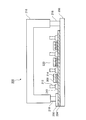
- FIG. 11 is a diagram illustrating an example of a display device using the organic electroluminescent element in this embodiment.
- a display device 200 shown in FIG. 11 is a so-called passive matrix display device, and includes a display device substrate 202, an anode wiring 204, an anode auxiliary wiring 206, a cathode wiring 208, an insulating film 210, a cathode partition wall 212, and an organic electroluminescent element. 214, a sealing plate 216, and a sealing material 218.
- the display device substrate 202 for example, a transparent substrate such as a rectangular glass substrate can be used.
- the thickness of the display device substrate 202 is not particularly limited, but for example, a thickness of 0.1 to 1 mm can be used.
- a plurality of anode wirings 204 are formed on the display device substrate 202.
- the anode wirings 204 are arranged in parallel at a constant interval.
- the anode wiring 204 is made of a transparent conductive film, and for example, ITO (Indium Tin Oxide) can be used.
- the thickness of the anode wiring 204 can be set to 100 nm to 150 nm, for example.
- An anode auxiliary wiring 206 is formed on the end of each anode wiring 204.
- the anode auxiliary wiring 206 is electrically connected to the anode wiring 204.
- the anode auxiliary wiring 206 functions as a terminal for connecting to the external wiring on the end side of the display device substrate 202, and the anode auxiliary wiring 206 is connected from a driving circuit (not shown) provided outside. A current can be supplied to the anode wiring 204 through the wiring.
- the anode auxiliary wiring 206 is made of a metal film having a thickness of 500 nm to 600 nm, for example.
- a plurality of cathode wirings 208 are provided on the display device substrate 202.
- the plurality of cathode wirings 208 are arranged so as to be parallel to each other and orthogonal to the anode wiring 204.
- As the cathode wiring 208 Al or an Al alloy can be used.
- the thickness of the cathode wiring 208 is, for example, 100 nm to 150 nm.
- a cathode auxiliary wiring (not shown) is provided at the end of the cathode wiring 208 and is electrically connected to the cathode wiring 208. Therefore, current can flow between the cathode wiring 208 and the cathode auxiliary wiring.
- An insulating film 210 is formed on the display device substrate 202 so as to cover the anode wiring 204.
- the insulating film 210 is provided with a rectangular opening 220 so as to expose a part of the anode wiring 204.
- the plurality of openings 220 are arranged in a matrix on the anode wiring 204.
- an organic electroluminescent element 214 is provided between the anode wiring 204 and the cathode wiring 208 as described later. That is, each opening 220 is a pixel. Accordingly, a display area is formed corresponding to the opening 220.
- the film thickness of the insulating film 210 can be, for example, 200 nm to 300 nm, and the size of the opening 220 can be, for example, 300 ⁇ m ⁇ 300 ⁇ m.
- An organic electroluminescent element 214 is formed at a location corresponding to the position of the opening 220 on the anode wiring 204.
- the organic electroluminescent element 214 since the anode wiring 204 replaces the substrate 11, the anode layer 12, the dielectric layer 13, the cathode layer 14, and the light emitting portion 17 (FIG. 1) are directly formed on the anode wiring 204. Reference) is formed.
- the organic electroluminescent element 214 is sandwiched between the anode wiring 204 and the cathode wiring 208 in the opening 220.
- the anode layer 12 of the organic electroluminescent element 214 is in contact with the anode wiring 204, and the cathode layer 14 is in contact with the cathode wiring 208.
- the thickness of the organic electroluminescent element 214 can be set to, for example, 150 nm to 200 nm.
- a plurality of cathode partitions 212 are formed on the insulating film 210 along a direction perpendicular to the anode wiring 204.
- the cathode partition 212 plays a role in spatially separating the plurality of cathode wirings 208 so that the wirings of the cathode wirings 208 are not electrically connected to each other. Accordingly, the cathode wiring 208 is disposed between the adjacent cathode partition walls 212.
- a cathode partition with a height of 2 to 3 ⁇ m and a width of 10 ⁇ m can be used.
- the display device substrate 202 is bonded through a sealing plate 216 and a sealing material 218. Thereby, the space in which the organic electroluminescent element 214 is provided can be sealed, and the organic electroluminescent element 214 can be prevented from being deteriorated by moisture in the air.
- a sealing plate 216 for example, a glass substrate having a thickness of 0.7 mm to 1.1 mm can be used.
- a current is supplied to the organic electroluminescent element 214 via the anode auxiliary wiring 206 and the cathode auxiliary wiring (not shown) by a driving device (not shown), the light emitting unit 17 is caused to emit light, and the recess 16 Can emit light.
- An image can be displayed on the display device 200 by controlling light emission and non-light emission of the organic electroluminescence element 214 corresponding to the above-described pixel by the control device.
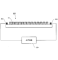
- FIG. 12 is a diagram illustrating an example of a lighting device including the organic electroluminescent element in the present embodiment.
- the lighting device 300 shown in FIG. 12 is installed adjacent to the organic electroluminescent element 10 and the substrate 11 (see FIG. 1) of the organic electroluminescent element 10 and connected to the anode layer 12 (see FIG. 1).
- the lighting circuit 301 has a DC power source (not shown) and a control circuit (not shown) inside, and supplies a current between the anode layer 12 and the cathode layer 14 of the organic electroluminescent element 10 through the terminal 302 and the terminal 303. And the organic electroluminescent element 10 is driven, the light emission part 17 (refer FIG. 1) is light-emitted, light is radiate
- the light emitting unit 17 may be made of a light emitting material that emits white light, and the organic electroluminescent element 10 using a light emitting material that emits green light (G), blue light (B), and red light (R). A plurality of them may be provided, and the combined light may be white.
- the lighting device 300 of the present embodiment when light is emitted with the diameter and interval of the recesses 16 (see FIG. 1) being reduced, it appears to the human eye to emit light.
- Example 1 [Preparation of phosphorescent polymer compound]
- E-2 iridium complex having a polymerizable substituent
- E-54 hole transporting compound
- E-66 Electron transporting compound
- V-601 Wako Pure Chemical Industries, Ltd.
- the reaction solution was dropped into acetone to cause precipitation, and the reprecipitation purification with dehydrated toluene-acetone was repeated three times to purify the phosphorescent polymer compound.
- dehydrated toluene and acetone those obtained by further distilling a high-purity grade manufactured by Wako Pure Chemical Industries, Ltd. were used.
- the solvent after the third reprecipitation purification was analyzed by high performance liquid chromatography, it was confirmed that no substance having absorption at 400 nm or more was detected in the solvent. That is, this means that the solvent contains almost no impurities, which means that the phosphorescent polymer compound has been sufficiently purified.
- the purified phosphorescent polymer compound was vacuum dried at room temperature for 2 days. As a result, it was confirmed by high performance liquid chromatography (detection wavelength 254 nm) that the phosphorescent polymer compound (ELP) obtained had a purity exceeding 99.9%.
- the organic electroluminescent element 10 shown in FIG. 1 was produced by the following method. Specifically, first, an ITO (Indium Tin Oxide) film having a thickness of 150 nm is formed on a glass substrate (25 mm square, 1 mm thickness) made of quartz glass using a sputtering apparatus (E-401s manufactured by Canon Anelva Co., Ltd.). A silicon (SiO 2 ) layer was formed to 200 nm, and an aluminum (Al) layer was formed to 100 nm.
- the glass substrate corresponds to the substrate 11.
- the ITO film corresponds to the anode layer 12
- the silicon dioxide layer corresponds to the dielectric layer 13
- the aluminum layer corresponds to the cathode layer 14, respectively.
- a photoresist (AZ 1500 made by AZ Electronic Materials Co., Ltd.) was formed to a thickness of about 1 ⁇ m by spin coating.
- a mask A corresponding to the pattern of the substantially circular recess 16 shown in FIG. 6 is prepared using quartz (plate thickness 3 mm) as a base material, and a stepper exposure apparatus (manufactured by Nikon, model NSR-1505i6) is used. Then, exposure was performed at 1/5 scale.
- the resist layer was patterned by developing with a 1.2% solution of TMAH (Tetra methyl ammonium hydroxide: (CH 3 ) 4 NOH). Thereafter, heat was applied at 130 ° C. for 10 minutes (post-baking treatment).
- TMAH Tetra methyl ammonium hydroxide: (CH 3 ) 4 NOH
- each layer was sequentially processed by dry etching using a reactive ion etching apparatus (RIE-200iP manufactured by Samco Corporation).
- RIE-200iP reactive ion etching apparatus manufactured by Samco Corporation.
- the glass substrate was washed by spraying pure water and dried using a spin dryer.
- the solution A was applied by a spin coating method (rotation speed: 3000 rpm), and then allowed to stand at 120 ° C. for 1 hour in a nitrogen atmosphere and dried to form the light emitting portion 17.
- the organic electroluminescent element 10 was able to be manufactured by the above process.
- Example 2 The organic electroluminescent element 10 was produced in the same manner as in Example 1 except that the pattern of the concave portion 16 was changed to the concave octagonal shape shown in FIG.
- Example 3 An organic electroluminescent element 10 was produced in the same manner as in Example 1 except that the pattern of the recess 16 was changed to the fractal structure shape shown in FIG.
- Example 4 The organic electroluminescence device 10 was produced in the same manner as in Example 1 except that the pattern of the recess 16 was changed to the fractal structure shape shown in FIG. 4A and each vertex of this shape was rounded. I did it.
- the R chamfering can be performed by adjusting the depth of focus of the stepper exposure apparatus by 5 mm (that is, so as to focus deeply on the photoresist surface).
- the organic electroluminescent element 10f shown in FIG. 9B was produced by the following method. Specifically, first, an ITO (Indium Tin Oxide) film having a thickness of 150 nm is formed on a glass substrate (25 mm square, 1 mm thickness) made of quartz glass using a sputtering apparatus (E-401s manufactured by Canon Anelva Co., Ltd.). A silicon (SiO 2 ) layer was formed to a thickness of 200 nm.
- the glass substrate corresponds to the substrate 11.
- the ITO film corresponds to the anode layer 12, and the silicon dioxide layer corresponds to the dielectric layer 13.
- a photoresist (AZ 1500 made by AZ Electronic Materials Co., Ltd.) was formed to a thickness of about 1 ⁇ m by spin coating.
- a mask A corresponding to the pattern of the concave decagonal shape 16 shown in FIG. 3B is prepared using quartz (plate thickness 3 mm) as a base material, and a stepper exposure apparatus (manufactured by Nikon Corporation, model number). NSR-1505i6) was used for exposure at 1/5 scale.
- the resist layer was patterned by developing with a 1.2% solution of TMAH (Tetra methyl ammonium hydroxide: (CH 3 ) 4 NOH). Thereafter, heat was applied at 130 ° C. for 10 minutes (post-baking treatment).
- TMAH Tetra methyl ammonium hydroxide: (CH 3 ) 4 NOH
- the silicon dioxide (SiO 2 ) layer was processed by dry etching using a reactive ion etching apparatus (RIE-200iP manufactured by Samco Corporation).
- RIE-200iP reactive ion etching apparatus
- the glass substrate was washed by spraying pure water and dried using a spin dryer.
- the solution A was applied by a spin coating method (rotation speed: 3000 rpm), and then allowed to stand at 120 ° C. for 1 hour in a nitrogen atmosphere and dried to form the light emitting portion 17.
- an aluminum (Al) layer having a thickness of 150 nm was formed as the cathode layer 14 using a sputtering apparatus (E-401s manufactured by Canon Anelva Co., Ltd.).
- the organic electroluminescent element 10f was able to be manufactured through the above steps.
- RIE-200iP reactive ion etching apparatus
- RIE-200iP reactive ion etching apparatus
- Example 8 As the organic electroluminescent element, the organic electroluminescent element 10h shown in FIG. 9D was produced by changing the following points from Example 6. A titanium (Ti) layer having a thickness of 150 nm was formed as the anode layer 12 in place of the ITO film using a sputtering apparatus (E-401s manufactured by Canon Anelva Co., Ltd.). The etching conditions for forming the recess 16 can be the same as those for the ITO film.
- Evaluation was performed by measuring the perimeter of the recess 16 and the maximum luminance of each organic electroluminescent element produced as described above. (Measurement of circumference) The circumference was measured based on the image of AFM (manufactured by Keyence, model VN8010) in which the shape of the recess 16 was observed. That is, the circumference of the concave portion 16 can be measured by tracing the outer circumference of the image of the concave portion 16 with a flexible ruler and calculating the length thereof.
- SYMBOLS 10 Organic electroluminescent element, 11 ... Board
Landscapes
- Physics & Mathematics (AREA)
- Optics & Photonics (AREA)
- Electroluminescent Light Sources (AREA)
Abstract
陽極層12と、陰極層14と、陽極層12と陰極層14の間に形成される誘電体層13と、少なくとも誘電体層13を貫通して形成される凹部16と、凹部16の内面と接触して形成され電流を供給することで光を発する発光部17と、を備え、凹部16の光の取り出し側から見た形状の周長が、形状を内包する最小円の周長より長いことを特徴とする有機電界発光素子10により、発光部での電荷集中が生じにくく、発光面の面積を有効に利用することができる有機電界発光素子等を提供する。
Description
本発明は、例えば、表示装置や照明装置に用いられる有機電界発光素子等に関する。
近年、エレクトロルミネセンス現象を利用したデバイスが重要度を増している。このようなデバイスとして、特に有機物質からなる発光材料を層状に形成し、この発光層に陽極と陰極とからなる一対の電極を設けて電圧を印加することで発光を行わせる有機電界発光素子が注目を集めている。有機電界発光素子は、陽極と陰極の間に電圧を印加することで、陽極と陰極からそれぞれ正孔と電子を注入し、注入された電子と正孔とが、発光層で結合することにより生じるエネルギーを利用して発光を行う。即ち、有機電界発光素子は、この結合によるエネルギーで発光層の発光材料が励起され、励起状態から再び基底状態に戻る際に光を発生する現象を利用したデバイスである。
この有機電界発光素子を表示装置として使用した場合、発光材料として有機物質を利用しているため、有機物質の選択によって色純度の高い光を発生させやすく、そのため色再現域を広くとることが可能であるという特徴がある。また有機電界発光素子は、自己発光であるため、表示装置として使用した場合に応答速度が速く、視野角が広いという特徴も有する。また有機電界発光素子の構造上から、表示装置の薄型化が容易になるという利点もある。更に、有機電界発光素子は、白色での発光も可能であり、面発光であることから、この有機電界発光素子を照明装置に組み込んで利用する用途も提案されている。
このような有機電界発光素子の構造として、例えば、特許文献1には、正孔電極注入層と電子注入電極層との間に挿入される誘電体層を備え、少なくとも誘電体層および電極層の一つを通って延び、正孔注入電極領域、電子注入電極領域および誘電体領域を備える内部キャビティ表面にエレクトロルミネセンスコーティング材料を塗布するキャビティ発光エレクトロルミネセンスデバイスが提案されている。
しかしながら、特表2003-522371号公報に記載されているようなキャビティ発光エレクトロルミネセンスデバイスは、キャビティの作製された箇所でしか発光を行わないため、発光面の面積を有効に使用しているとは言えない。また、キャビティ内部において電荷集中が生じやすいため、大きな電流を流して発光強度を大きくするのにも限度がある。
上記課題に鑑み、本発明の目的は、発光部での電荷集中が生じにくく、発光面の面積を有効に利用することができる有機電界発光素子を提供することである。
また、他の目的は、高いコントラストおよび解像度を有し、高い発光効率を有する表示装置を提供することである。
更に、他の目的は、高い発光効率を有する照明装置を提供することである。
また、他の目的は、高いコントラストおよび解像度を有し、高い発光効率を有する表示装置を提供することである。
更に、他の目的は、高い発光効率を有する照明装置を提供することである。
本発明の有機電界発光素子は、第1の電極層と、第2の電極層と、第1の電極層と第2の電極層の間に形成される誘電体層と、少なくとも誘電体層を貫通して形成される凹部と、凹部の内面と接触して形成され、電流を供給することで光を発する発光部と、を備え、凹部の光の取り出し側から見た形状の周長が、形状を内包する最小円の周長より長いことを特徴とする。
ここで、形状は、凹多角形形状であることが好ましく、凹多角形形状は、頂点を8以上有することが更に好ましい。また形状は、フラクタル構造を有する形状であることが好ましい。そして形状を構成する辺の長さは、略同一であることが好ましく、形状の頂点部を更に面取りする形状としたことが更に好ましい。更に第1の電極層を形成するための基板を更に有し、基板は、凹部に対応する位置に穿孔部を有することが好ましい。
また本発明の表示装置は、上記の有機電界発光素子を備えることを特徴とする。
また本発明の照明装置は、上記の有機電界発光素子を備えることを特徴とする。
本発明によれば、発光部での電荷集中が生じにくく、発光面の面積を有効に利用することができる有機電界発光素子等を提供できる。
以下、添付図面を参照して、本発明の実施の形態について詳細に説明する。
図1は、本実施の形態が適用される有機電界発光素子の一例を説明した部分断面図である。
図1に示した有機電界発光素子10は、基板11上に、正孔を注入するための第1の電極層としての陽極層12と、絶縁性の誘電体層13と、電子を注入するための第2の電極層としての陰極層14とが順に積層した構造を採る。また、陽極層12、誘電体層13、陰極層14を貫通して形成される凹部16を有し、そして凹部16の内面と接触して形成され電圧を印加することで発光する発光材料からなる発光部17を有する。この発光部17は、凹部16の全体を埋めずに凹部16の内面に発光材料が塗布され、第2凹部18を形成する。
図1は、本実施の形態が適用される有機電界発光素子の一例を説明した部分断面図である。
図1に示した有機電界発光素子10は、基板11上に、正孔を注入するための第1の電極層としての陽極層12と、絶縁性の誘電体層13と、電子を注入するための第2の電極層としての陰極層14とが順に積層した構造を採る。また、陽極層12、誘電体層13、陰極層14を貫通して形成される凹部16を有し、そして凹部16の内面と接触して形成され電圧を印加することで発光する発光材料からなる発光部17を有する。この発光部17は、凹部16の全体を埋めずに凹部16の内面に発光材料が塗布され、第2凹部18を形成する。
基板11は、陽極層12、誘電体層13、陰極層14、発光部17を形成する支持体となるものである。基板11には、有機電界発光素子10に要求される機械的強度を満たす材料が用いられる。
基板11の材料としては、有機電界発光素子10の基板11側から光を取り出したい場合は、可視光に対して透明であることが必要である。具体的には、ソーダガラス、無アルカリガラスなどのガラス;アクリル樹脂、メタクリル樹脂、ポリカーボネート樹脂、ポリエステル樹脂、ナイロン樹脂などの透明プラスチック;シリコン樹脂などである。
有機電界発光素子10の基板11側から光を取り出す必要がない場合は、基板11の材料としては、可視光に対して透明であるものに限られず、不透明なものも使用できる。具体的には、上記材料に加えて、シリコン(Si)、銅(Cu)、銀(Ag)、金(Au)、白金(Pt)、タングステン(W)、チタン(Ti)、タンタル(Ta)、もしくはニオブ(Nb)の単体、またはこれらの合金、あるいはステンレスなどからなる材料も使用することができる。
基板11の厚さは、要求される機械的強度にもよるが、好ましくは、0.1mm~10mm、より好ましくは0.25mm~2mmである。
基板11の材料としては、有機電界発光素子10の基板11側から光を取り出したい場合は、可視光に対して透明であることが必要である。具体的には、ソーダガラス、無アルカリガラスなどのガラス;アクリル樹脂、メタクリル樹脂、ポリカーボネート樹脂、ポリエステル樹脂、ナイロン樹脂などの透明プラスチック;シリコン樹脂などである。
有機電界発光素子10の基板11側から光を取り出す必要がない場合は、基板11の材料としては、可視光に対して透明であるものに限られず、不透明なものも使用できる。具体的には、上記材料に加えて、シリコン(Si)、銅(Cu)、銀(Ag)、金(Au)、白金(Pt)、タングステン(W)、チタン(Ti)、タンタル(Ta)、もしくはニオブ(Nb)の単体、またはこれらの合金、あるいはステンレスなどからなる材料も使用することができる。
基板11の厚さは、要求される機械的強度にもよるが、好ましくは、0.1mm~10mm、より好ましくは0.25mm~2mmである。
陽極層12は、陰極層14との間で電圧を印加し、発光部17に正孔を注入する。陽極層12に使用される材料としては、電気伝導性を有するものであれば、特に限定されるものではないが、-5℃~80℃の温度範囲で面抵抗が1000Ω以下であることが好ましく、100Ω以下であることが更に好ましい。加えて、アルカリ性水溶液に対し、電気抵抗が顕著に変化しないことが好ましい。
このような条件を満たす材料として、金属酸化物、金属、合金が使用できる。ここで、金属酸化物としては、例えば、ITO(酸化インジウムスズ)、IZO(インジウム-亜鉛酸化物)が挙げられる。また金属としては、ステンレス、銅(Cu)、銀(Ag)、金(Au)、白金(Pt)、タングステン(W)、チタン(Ti)、タンタル(Ta)、ニオブ(Nb)等が挙げられる。そしてこれらの金属を含む合金も使用できる。但し、陽極層12は、有機電界発光素子10の基板11側から光を取り出したいときは、透明電極であることが必要である。透明電極を形成するのに用いられる透明材料としては、例えば、酸化インジウム、酸化亜鉛、酸化スズ、それらの複合体であるITO(酸化インジウムスズ)、IZO(インジウム-亜鉛酸化物)等からなる導電性ガラス(NESA等)、金、白金、銀、銅が挙げられる。これらの中でも、ITO、IZO、酸化スズが好ましい。また、ポリアニリンもしくはその誘導体、ポリチオフェンもしくはその誘導体等の有機物からなる透明導電膜を用いてもよい。また、発光部17への正孔の注入を容易にするという観点から、陽極層12の発光部17と接触する表面上に、フタロシアニン誘導体、ポリチオフェン誘導体等の導電性高分子、Mo酸化物、アモルファスカーボン、フッ化カーボン、ポリアミン化合物等からなる1nm~200nmの層、あるいは金属酸化物、金属フッ化物、有機絶縁材料等からなる平均膜厚10nm以下の層を設けてもよい。
陽極層12の厚さは、有機電界発光素子10の基板11側から光を取り出したい場合は、高い光透過率を要求されるため、2nm~300nmであることが好ましい。また有機電界発光素子10の基板11側から光を取り出す必要がない場合は、例えば、2nm~2mmで形成することができる。
なお、陽極層12は、基板11と同一の材質を使用することもできる。この場合、陽極層12と基板11は一体となる。
このような条件を満たす材料として、金属酸化物、金属、合金が使用できる。ここで、金属酸化物としては、例えば、ITO(酸化インジウムスズ)、IZO(インジウム-亜鉛酸化物)が挙げられる。また金属としては、ステンレス、銅(Cu)、銀(Ag)、金(Au)、白金(Pt)、タングステン(W)、チタン(Ti)、タンタル(Ta)、ニオブ(Nb)等が挙げられる。そしてこれらの金属を含む合金も使用できる。但し、陽極層12は、有機電界発光素子10の基板11側から光を取り出したいときは、透明電極であることが必要である。透明電極を形成するのに用いられる透明材料としては、例えば、酸化インジウム、酸化亜鉛、酸化スズ、それらの複合体であるITO(酸化インジウムスズ)、IZO(インジウム-亜鉛酸化物)等からなる導電性ガラス(NESA等)、金、白金、銀、銅が挙げられる。これらの中でも、ITO、IZO、酸化スズが好ましい。また、ポリアニリンもしくはその誘導体、ポリチオフェンもしくはその誘導体等の有機物からなる透明導電膜を用いてもよい。また、発光部17への正孔の注入を容易にするという観点から、陽極層12の発光部17と接触する表面上に、フタロシアニン誘導体、ポリチオフェン誘導体等の導電性高分子、Mo酸化物、アモルファスカーボン、フッ化カーボン、ポリアミン化合物等からなる1nm~200nmの層、あるいは金属酸化物、金属フッ化物、有機絶縁材料等からなる平均膜厚10nm以下の層を設けてもよい。
陽極層12の厚さは、有機電界発光素子10の基板11側から光を取り出したい場合は、高い光透過率を要求されるため、2nm~300nmであることが好ましい。また有機電界発光素子10の基板11側から光を取り出す必要がない場合は、例えば、2nm~2mmで形成することができる。
なお、陽極層12は、基板11と同一の材質を使用することもできる。この場合、陽極層12と基板11は一体となる。
誘電体層13は、陽極層12と陰極層14の間に形成され、陽極層12と陰極層14とを所定の間隔にて分離し絶縁すると共に、発光部17に電圧を印加するためのものである。このため誘電体層13は高抵抗率材料であることが必要であり、抵抗率としては、108Ω・cm以上、好ましくは1012Ω・cm以上有することが要求される。具体的な材料としては、窒化ケイ素、窒化ホウ素、窒化アルミニウム等の金属窒化物;酸化珪素、酸化アルミニウム等の金属酸化物が挙げられるが、他にポリイミド、ポリフッ化ビニリデン、パリレン等の高分子化合物も使用可能である。
また誘電体層13は電気的絶縁性が保持される限りは、二層以上で構成されていてもよい。具体的には、絶縁体からなる層に追加して、絶縁体からなる層、導電体からなる層、絶縁体に導電体を分散させた層、絶縁体に絶縁体を分散させた層、半導体からなる層、等を積層させてもよい。追加する層に用いられる材料に特に制約はないが、具体的には、窒化ケイ素、窒化ホウ素、窒化アルミニウム等の金属窒化物;酸化珪素、酸化アルミニウム、酸化インジウム、酸化亜鉛、酸化スズ、それらの複合体であるITO(酸化インジウムスズ)、IZO(インジウム-亜鉛酸化物)等の金属酸化物;ステンレス、銅(Cu)、銀(Ag)、金(Au)、白金(Pt)、タングステン(W)、チタン(Ti)、タンタル(Ta)、ニオブ(Nb)等の金属;導電性ポリマー、有機EL発光材料等の有機導電性材料;グラファイト、アルミナ、窒化ホウ素、カーボンナノチューブ、粉末ダイヤモンド、粉末珪素等を樹脂等の絶縁体に分散させたものが挙げられる。
誘電体層13の厚さとしては、有機電界発光素子10全体の厚さを抑えるために1μmを越えないことが好ましい。また、陽極層12と陰極層14との間隔が狭い方が、発光のために必要な電圧が低くて済むので、この観点からも誘電体層14は薄い方がより好ましい。但し、薄すぎると有機電界発光素子10を駆動するための電圧に対し、絶縁耐力が十分でなくなるおそれがある。ここで絶縁耐力は、発光部17が形成されていない状態で、陽極層12と陰極層14の間に流れる電流の電流密度が、0.1mA/cm2以下であることが好ましく、0.01mA/cm2以下であることがより好ましい。また有機電界発光素子10の駆動電圧に対し、2Vを超えた電圧に耐えることが好ましいため、例えば、駆動電圧が5Vである場合は、発光部17が形成されていない状態で、陽極層12と陰極層14の間に約7Vの電圧を印加した場合に上記の電流密度を満たすことが必要である。これを満たす誘電体層13の厚さとしては、好ましくは、10nm~500nm、更に好ましくは50nm~200nmで作製するのがよい。
陰極層14は、陽極層12との間で電圧を印加し、発光部17に電子を注入する。陰極層14に使用される材料としては、陽極層12と同様に電気伝導性を有するものであれば、特に限定されるものではないが、仕事関数が低く、かつ化学的に安定なものが好ましい。仕事関数は、化学的安定性を考慮すると-2.9eV以下であることが好ましい。具体的には、Al、MgAg合金、AlLiやAlCaなどのAlとアルカリ金属の合金等の材料を例示することができる。陰極層14の厚さは10nm~1μmが好ましく、50nm~500nmがより好ましい。
また、陰極層14から発光部17への電子の注入障壁を下げて電子の注入効率を上げる目的で、図示しない陰極バッファー層を、陰極層14に隣接して設けてもよい。陰極バッファー層は、陰極層14より仕事関数の低いことが必要であり、金属材料が好適に用いられる。例えば、アルカリ金属(Na、K、Rb、Cs)、アルカリ土類金属(Sr、Ba、Ca、Mg)、希土類金属(Pr、Sm、Eu、Yb)、あるいはこれら金属のフッ化物、塩化物、酸化物から選ばれる単体あるいは2つ以上の混合物を使用することができる。陰極バッファー層の厚さは0.05nm~50nmが好ましく、0.1nm~20nmがより好ましく、0.5nm~10nmがより一層好ましい。
凹部16は、発光部17をその内面に塗布し、かつ発光部17からの光を取り出すためのものであり、本実施の形態では、第1の電極層である陽極層12、誘電体層13、第2の電極層である陰極層14を貫通するように形成する。このように凹部16を設けることにより発光部17から発せられた光は、凹部16の内部を伝搬し、基板11側および陰極層14の側の両方向において取り出すことができる。ここで、凹部16は、陽極層12、誘電体層13、陰極層14を貫通して形成されているため、第1の電極層である陽極層12および第2の電極層である陰極層14が不透明材料により形成されるときでも光を取り出すことが可能である。
図2は、本実施の形態が適用される有機電界発光素子10の凹部16の形状とその配列を説明した図である。ここで、図2は、有機電界発光素子10を光の取り出し方向から見た図である。
図2において凹部16は、詳しくは後述するが凹八角形の形状を採る。そして、この凹部16は、3列配列し、隣接する各列は、それぞれ千鳥状になるように配列する。そして、この凹八角形を内包する最小円21(最小内包円)を考え、この隣接する最小円21の中心同士を結ぶ各線分が、正三角形を構成するように配列する。ここで、この正三角形の一辺の長さをピッチ(P)とし、隣接する最小円21の外縁部の距離を隔離(s)とすると、最小円21の半径(r)との間に、p=s+2rの関係が成り立つ。なお本実施の形態において、「最小内包円」とは、凹部16が採る形状を全て内側に含む円のうち最小のものを言う。
図2において凹部16は、詳しくは後述するが凹八角形の形状を採る。そして、この凹部16は、3列配列し、隣接する各列は、それぞれ千鳥状になるように配列する。そして、この凹八角形を内包する最小円21(最小内包円)を考え、この隣接する最小円21の中心同士を結ぶ各線分が、正三角形を構成するように配列する。ここで、この正三角形の一辺の長さをピッチ(P)とし、隣接する最小円21の外縁部の距離を隔離(s)とすると、最小円21の半径(r)との間に、p=s+2rの関係が成り立つ。なお本実施の形態において、「最小内包円」とは、凹部16が採る形状を全て内側に含む円のうち最小のものを言う。
ここで、凹部16がこの最小円21の形状であった場合は、図1からもわかるように発光部17は、この円形形状の外縁部に沿って円形状に形成される。そのため、発光はこの最小円21の外縁部で円形状に生じる。そして、それぞれの間隔である隔離(s)を小さくすれば、それだけ単位面積当たりの凹部16の数が増加するため、発光強度を大きくすることができる。しかしながら、有機電界発光素子10の製造上の問題から、凹部16を最小円21の形状とした場合、隔離(s)をむやみに小さくすることは困難である。
そこで、本実施の形態では、凹部16の光の取り出し側から見た形状の周長が、この形状を内包する最小円21の周長より長くすることとしている。
図3(a)~(b)は、本実施の形態の有機電界発光素子10における凹部16の形状を説明した図である。
図3(a)~(b)に示した凹部16は、有機電界発光素子10の光の取り出し方向から見た場合の形状である。ここで、図3(a)に示した凹部16の場合、図2で示した凹部16と同様の形状である。この凹部16の形状は、凹多角形形状の1つである凹八角形である。またこの凹八角形を構成する辺の長さは略同一である。そして、この辺の長さの合計としての周長は、凹八角形を内包する最小円21の周長(即ち、円周の長さ)より長くなっている。
また、図3(b)に示した凹部16の場合、凹部16の形状は、凹多角形の1つである凹十角形であり、いわゆる星形形状となっている。そして、この凹十角形の凸部の頂点における頂角は、36°としている。またこの凹十角形を構成する辺の長さはやはり略同一である。そして、この辺の長さの合計としての周長は、凹十角形を内包する最小円21の周長より長くなっている。
なお本実施の形態において、「凹多角形」とは、180度以上の内角を有する多角形のことである。凹部16の形状として凹多角形形状を採る場合、その凹多角形形状は、頂点を8以上有することが好ましい。頂点を8以上有することで凹多角形の周長が、凹多角形を内包する最小円21の周長より長くなりやすくなる。
図3(a)~(b)は、本実施の形態の有機電界発光素子10における凹部16の形状を説明した図である。
図3(a)~(b)に示した凹部16は、有機電界発光素子10の光の取り出し方向から見た場合の形状である。ここで、図3(a)に示した凹部16の場合、図2で示した凹部16と同様の形状である。この凹部16の形状は、凹多角形形状の1つである凹八角形である。またこの凹八角形を構成する辺の長さは略同一である。そして、この辺の長さの合計としての周長は、凹八角形を内包する最小円21の周長(即ち、円周の長さ)より長くなっている。
また、図3(b)に示した凹部16の場合、凹部16の形状は、凹多角形の1つである凹十角形であり、いわゆる星形形状となっている。そして、この凹十角形の凸部の頂点における頂角は、36°としている。またこの凹十角形を構成する辺の長さはやはり略同一である。そして、この辺の長さの合計としての周長は、凹十角形を内包する最小円21の周長より長くなっている。
なお本実施の形態において、「凹多角形」とは、180度以上の内角を有する多角形のことである。凹部16の形状として凹多角形形状を採る場合、その凹多角形形状は、頂点を8以上有することが好ましい。頂点を8以上有することで凹多角形の周長が、凹多角形を内包する最小円21の周長より長くなりやすくなる。
図3(a)~(b)のように凹部16を形成することで、凹部16の形状を単純に円形形状とする場合より、凹部16内の発光面積が増大する。そのため有機電界発光素子10に一定電流を流した場合、単位発光面積に流れる電流量は円形形状と比較して減少することになる。よって、凹部16内の電流密度を下げることができる。電流密度が下がると、電流に対する発光効率である電流発光効率を上げることができると共に、有機電界発光素子10に印加する電圧を下げることも可能となる。その結果、むやみに隔離(s)(図2参照)を小さくしなくても発光強度を大きくすることが可能となり、発光面の面積を有効に利用することができる。更に、凹部16内の発光面積が増大することにより発光部17より発生する熱を放熱する効率も上昇する。そのため、有機電界発光素子10の長寿命化を図りやすくなる。
また、辺の長さを略同一とすることにより、更に特定の部分への電荷集中を抑制することができる。なおここで、辺の長さが略同一とは、厳密な意味で同一の長さであることを意味するわけではなく、概ね同一の長さであればよいことを意味する。
また、本実施の形態では、凹部16の光の取り出し側から見た形状の周長と、この形状を内包する最小円21の周長を比較するのに「エッジ密度」という指標を用いることができる。
このエッジ密度は、単位面積当たりの凹部16のエッジの長さ、即ち周長を表す。
例えば、円形状の凹部16が、図2で示したように配列する場合は、この凹部16の配列の繰り返し単位は、正三角形となることからこの正三角形内に属する部分の周長をまず計算する。凹部16が円形形状の場合は、この正三角形の1つの角の部分に属するこの円の周長(即ち、円周長)は円の周長の1/6である。そして、正三角形の角は3つあり、円の半径はrなので、この正三角形内に属する円形形状の周長は、3×(1/6)×(円周長)=πrである。
そして、この正三角形の面積は、一辺の長さがpであることより、√3p2/4である。よって、単位面積当たりの凹部16のエッジの長さであるエッジ密度は、4√3πr/(3p2)であり、これは、7.26r/p2と近似できる。
このエッジ密度は、単位面積当たりの凹部16のエッジの長さ、即ち周長を表す。
例えば、円形状の凹部16が、図2で示したように配列する場合は、この凹部16の配列の繰り返し単位は、正三角形となることからこの正三角形内に属する部分の周長をまず計算する。凹部16が円形形状の場合は、この正三角形の1つの角の部分に属するこの円の周長(即ち、円周長)は円の周長の1/6である。そして、正三角形の角は3つあり、円の半径はrなので、この正三角形内に属する円形形状の周長は、3×(1/6)×(円周長)=πrである。
そして、この正三角形の面積は、一辺の長さがpであることより、√3p2/4である。よって、単位面積当たりの凹部16のエッジの長さであるエッジ密度は、4√3πr/(3p2)であり、これは、7.26r/p2と近似できる。
このエッジ密度を図3(a)~(b)に示した凹多角形で計算する。まず図3(a)に示した凹八角形の場合は、一辺の長さをrの4/5、即ち、4r/5とした場合の凹八角形では、エッジ密度は、64√3r/(15p2)である。これは、7.39r/p2と近似できる。
また、図3(b)に示した凹十角形の場合は、エッジ密度は、20√3(3-√5)rsin72°/(3p2)となる。これは、8.39r/p2と近似できる。
よって、いずれも7.26r/p2よりエッジ密度は大きくなるため、凹部16の光の取り出し側から見た形状の周長は、この形状を内包する最小円21の周長より長くなっている。
また、図3(b)に示した凹十角形の場合は、エッジ密度は、20√3(3-√5)rsin72°/(3p2)となる。これは、8.39r/p2と近似できる。
よって、いずれも7.26r/p2よりエッジ密度は大きくなるため、凹部16の光の取り出し側から見た形状の周長は、この形状を内包する最小円21の周長より長くなっている。
なお、有機電界発光素子10の光の取り出し方向から見た場合の凹部16の形状を上述した凹多角形ではなく、凸多角形を使用した場合は、凹部16の光の取り出し側から見た形状の周長が、この形状を内包する最小円21の周長より長くすることはできない。
例えば、凸多角形として正三角形を考え、この正三角形を内包する最小円21の半径をrとした場合のエッジ密度は、6r/p2となる。また凸多角形として正方形を考えた場合のエッジ密度は、8√6r/(3p2)となる。これは6.53r/p2と近似できる。いずれも円形形状の場合の7.26r/p2を下回る。凸多角形の辺の数を増やせば、エッジ密度は、この凸多角形を内包する最小円21のエッジ密度に近づくが、超えることはできない。
また、有機電界発光素子10の光の取り出し方向から見た場合の凹部16の形状は凹多角形である必要はなく他の形状でもよい。
図4(a)は、本実施の形態の有機電界発光素子10における凹部16の他の形状を説明した図である。
図4(a)に示した凹部16の形状は、フラクタル構造を有する形状である。
この形状は、正三角形の各辺を構成する3つの線分をそれぞれコッホ曲線とする変形を行う際に途中で出現する形状である。
図4(a)は、本実施の形態の有機電界発光素子10における凹部16の他の形状を説明した図である。
図4(a)に示した凹部16の形状は、フラクタル構造を有する形状である。
この形状は、正三角形の各辺を構成する3つの線分をそれぞれコッホ曲線とする変形を行う際に途中で出現する形状である。
図4(b)~(d)にこの形状の作成方法を示した。まず、正三角形が出発となる形状である(図4(b))。次に正三角形の辺を構成する3つの各線分を3等分し、分割した2点を頂点とする正三角形の作図を行う(図4(c))。これにより12個の辺からなる形状ができる。そしてこの12個の辺の長さは全て同じであり、その長さの合計は、元の正三角形の4/3倍となる。次にこの12個の辺の全てについて、図4(b)で行ったのと同様の操作を更に行う(図4(d))。これにより、48個の辺からなる図4(a)で示した形状ができる。そしてこの48個の辺の長さは全て同じであり、その長さの合計は、元の正三角形の4/3×4/3倍=16/9倍となる。
このようにして作成した形状は、本実施の形態では、元の形状である図4(b)の正三角形を第1世代とし、図4(c)の形状を第2世代、図4(d)(図4(a))の形状を第3世代と呼ぶことにする。この各形状は、この形状の各部分を拡大すると全体と同じ形になる自己相似性を有する。
ここで、図4(c)の形状について、この形状を内包する最小円21の半径をrとした場合のエッジ密度を計算すると、8r/p2となり、この最小円21のエッジ密度である7.26r/p2を上回る。
また、図4(a)(図4(d))の形状について、この形状を内包する最小円21の半径をrとした場合のエッジ密度を計算すると、32r/(3p2)となる。これは、10.67r/p2と近似でき、更にエッジ密度を大きくすることができる。
また、図4(a)(図4(d))の形状について、この形状を内包する最小円21の半径をrとした場合のエッジ密度を計算すると、32r/(3p2)となる。これは、10.67r/p2と近似でき、更にエッジ密度を大きくすることができる。
なお、図4(b)~(d)に示したフラクタル構造を有する形状は、正三角形を出発形状とし、その第2世代~第3世代の形状を示したが、これに限られるものではない。例えば、正方形、正五角形、正六角形等を出発形状としてもよい。また凹部16の光の取り出し側から見た形状として好ましい世代については、凹部16の作製の容易性の観点から、第2世代~第4世代で作成することができる形状がよい。
なお、凹部16内部での特定の部分への電荷集中を抑制する観点からは、上述したような各辺の長さが等しい凹多角形や、フラクタル構造を有する形状が好ましいが、これに限られるものではない。
図5(a)~(b)は、本実施の形態の有機電界発光素子10における凹部16の更に他の形状を説明した図である。
図5(a)に示した凹部16の形状は、凹多角形であるが、各辺の長さは略同一ではなく、種々の長さを採る。このような形状でも、形状の周長をこの形状を内包する最小円21の周長より長くすることができる。
また、上述した例では、各形状は、複数の線分により形成されていたが、これに限られるものではなく、曲線により構成されていてもよい。
図5(b)に示した凹部16の形状は、この場合の一例を示したものであり、凹部16の形状は不規則な曲線により構成されている。そして、形状の周長は、この形状を内包する最小円21の周長より長くなっている。
図5(a)~(b)は、本実施の形態の有機電界発光素子10における凹部16の更に他の形状を説明した図である。
図5(a)に示した凹部16の形状は、凹多角形であるが、各辺の長さは略同一ではなく、種々の長さを採る。このような形状でも、形状の周長をこの形状を内包する最小円21の周長より長くすることができる。
また、上述した例では、各形状は、複数の線分により形成されていたが、これに限られるものではなく、曲線により構成されていてもよい。
図5(b)に示した凹部16の形状は、この場合の一例を示したものであり、凹部16の形状は不規則な曲線により構成されている。そして、形状の周長は、この形状を内包する最小円21の周長より長くなっている。
また図6に示した凹部16は、凹部16の形状が曲線により構成される他の一例を示したものである。この凹部16は、規則性を有する曲線により構成される略円形の形状となっている。この場合でも、凹部16の形状の周長をこの形状を内包する最小円21の周長より長くすることができる。
なお、今まで詳述した凹部16の形状では、特に頂点部において、電荷集中が生じるおそれがある。これを防止するために、例えば、頂点部を更に面取りする形状にすることが考えられる。
図7(a)~(c)は、凹十角形を2通りの方法で面取りした場合を説明した図である。
まず図7(b)は、図7(a)で示す凹十角形の各頂点をR面取りした場合である。この面取りにより各頂点は円弧状になだらかに丸められる。また図7(c)は、図7(a)で示す凹十角形の各頂点をC面取りした場合である。この面取りにより各頂点は、直線状に丸められる。何れの場合も頂点部を面取りを行う前よりなだらかな形状にすることができるため、この部分における電荷集中を抑制することができる。なお図7(b)~(c)で示した例では、全ての頂点部について面取りを行ったが、各頂点部のうち凸部に対して行うことが特に好ましい。即ち、凸部においては鋭角をなすため、電荷集中が起こりやすいためであり、この部分の面取りを行うことにより、より効果的に電荷集中を抑制することができる。
まず図7(b)は、図7(a)で示す凹十角形の各頂点をR面取りした場合である。この面取りにより各頂点は円弧状になだらかに丸められる。また図7(c)は、図7(a)で示す凹十角形の各頂点をC面取りした場合である。この面取りにより各頂点は、直線状に丸められる。何れの場合も頂点部を面取りを行う前よりなだらかな形状にすることができるため、この部分における電荷集中を抑制することができる。なお図7(b)~(c)で示した例では、全ての頂点部について面取りを行ったが、各頂点部のうち凸部に対して行うことが特に好ましい。即ち、凸部においては鋭角をなすため、電荷集中が起こりやすいためであり、この部分の面取りを行うことにより、より効果的に電荷集中を抑制することができる。
発光部17は、電圧を印加することで発光する発光材料であり、上述の通り凹部16に接触して発光材料が設けられることにより第2凹部18を形成するように凹部16の内面に塗布される。発光部17において、陽極層12から注入された正孔と陰極層15から注入された電子とが再結合し、発光が生じる。
発光部17の材料としては、低分子化合物及び高分子化合物のいずれをも使用することができる。例えば、大森裕:応用物理、第70巻、第12号、1419-1425頁(2001年)に記載されている発光性低分子化合物及び発光性高分子化合物などを例示することができる。
但し、本実施の形態では、塗布性に優れた材料が好ましい。即ち本実施の形態における有機電界発光素子10の構造では、発光部17が凹部16内で安定に発光するためには発光部17が凹部16の内面に均一に接し、膜厚が均等に成膜されること、即ちカバレッジ性が向上することが好ましい。塗布性に優れた材料を使用せずに発光部17を形成すると、凹部16全体に発光部17が一様に接していない、あるいは凹部16内面の膜厚が均一でない成膜状態になりやすい。そのため凹部16から出射する光の輝度のばらつき等を生じやすくなる。
また、凹部16内に発光部17を均一に形成するためには、塗布法で行うことが好ましい。即ち、塗布法では、凹部16に発光材料を含むインクを埋め込むことが容易であるため凹凸を有する面においてもカバレッジ性を高めて成膜することが可能である。塗布法においては塗布性を向上させる目的で、主に重量平均分子量が1,000~2,000,000である材料が好適に用いられる。また、塗布性を向上させるためレベリング剤、脱泡剤などの塗布性向上添加剤を添加したり、電荷トラップ能力の少ないバインダー樹脂を添加することもできる。
また、凹部16内に発光部17を均一に形成するためには、塗布法で行うことが好ましい。即ち、塗布法では、凹部16に発光材料を含むインクを埋め込むことが容易であるため凹凸を有する面においてもカバレッジ性を高めて成膜することが可能である。塗布法においては塗布性を向上させる目的で、主に重量平均分子量が1,000~2,000,000である材料が好適に用いられる。また、塗布性を向上させるためレベリング剤、脱泡剤などの塗布性向上添加剤を添加したり、電荷トラップ能力の少ないバインダー樹脂を添加することもできる。
具体的に、塗布性に優れる材料としては、例えば、特開2007-86639号公報に挙げられている所定の構造を有する分子量1500以上6000以下のアリールアミン化合物や、特開2000-034476号公報に挙げられている所定の高分子蛍光体などが挙げられる。
ここで、塗布性に優れた材料の中でも、有機電界発光素子10の製造のプロセスが簡素化されるという点で発光性高分子化合物が好ましく、発光効率が高い点で燐光発光性化合物が好ましい。従って、特に燐光発光性高分子化合物が好ましい。なお、複数の材料同士を混合、あるいは塗布性を損なわない範囲で低分子発光材料(例えば、分子量1000以下)を添加することも可能である。この際の低分子発光材料の添加量は30wt%以下が好ましい。
また、発光性高分子化合物は、共役発光性高分子化合物と非共役発光性高分子化合物とに分類することもできるが、中でも非共役発光性高分子化合物が好ましい。
上記の理由から、本実施の形態で用いられる発光材料としては、燐光発光性非共役高分子化合物(燐光発光性高分子であり、かつ非共役発光性高分子化合物でもある発光材料)が特に好ましい。
ここで、塗布性に優れた材料の中でも、有機電界発光素子10の製造のプロセスが簡素化されるという点で発光性高分子化合物が好ましく、発光効率が高い点で燐光発光性化合物が好ましい。従って、特に燐光発光性高分子化合物が好ましい。なお、複数の材料同士を混合、あるいは塗布性を損なわない範囲で低分子発光材料(例えば、分子量1000以下)を添加することも可能である。この際の低分子発光材料の添加量は30wt%以下が好ましい。
また、発光性高分子化合物は、共役発光性高分子化合物と非共役発光性高分子化合物とに分類することもできるが、中でも非共役発光性高分子化合物が好ましい。
上記の理由から、本実施の形態で用いられる発光材料としては、燐光発光性非共役高分子化合物(燐光発光性高分子であり、かつ非共役発光性高分子化合物でもある発光材料)が特に好ましい。
本発明の有機電界発光素子10における発光部17は、好ましくは、燐光を発光する燐光発光性単位とキャリアを輸送するキャリア輸送性単位とを一つの分子内に備えた、燐光発光性高分子(燐光発光材料)を少なくとも含む。燐光発光性高分子は、重合性置換基を有する燐光発光性化合物と、重合性置換基を有するキャリア輸送性化合物とを共重合することによって得られる。燐光発光性化合物はイリジウム(Ir)、白金(Pt)および金(Au)の中から一つ選ばれる金属元素を含む金属錯体であり、中でもイリジウム錯体が好ましい。
燐光発光性化合物における重合性置換基としては、例えば、ビニル基、アクリレート基、メタクリレート基、メタクリロイルオキシエチルカルバメート基等のウレタン(メタ)アクリレート基、スチリル基及びその誘導体、ビニルアミド基及びその誘導体などが挙げられ、中でもビニル基、メタクリレート基、スチリル基及びその誘導体が好ましい。これらの置換基は、ヘテロ原子を有してもよい炭素数1~20の有機基を介して金属錯体に結合していてもよい。
重合性置換基を有するキャリア輸送性化合物は、ホール輸送性および電子輸送性の内のいずれか一方または両方の機能を有する有機化合物における一つ以上の水素原子を重合性置換基で置換した化合物を挙げることができる。
重合性置換基を有するキャリア輸送性化合物は、ホール輸送性および電子輸送性の内のいずれか一方または両方の機能を有する有機化合物における一つ以上の水素原子を重合性置換基で置換した化合物を挙げることができる。
キャリア輸送性化合物における重合性置換基はビニル基であるが、ビニル基をアクリレート基、メタクリレート基、メタクリロイルオキシエチルカルバメート基等のウレタン(メタ)アクリレート基、スチリル基及びその誘導体、ビニルアミド基及びその誘導体などの重合性置換基で置換した化合物であってもよい。また、これらの重合性置換基は、ヘテロ原子を有してもよい炭素数1~20の有機基を介して結合していてもよい。
重合性置換基を有する燐光発光性化合物と、重合性置換基を有するキャリア輸送性化合物の重合方法は、ラジカル重合、カチオン重合、アニオン重合、付加重合のいずれでもよいが、ラジカル重合が好ましい。また、重合体の分子量は重量平均分子量で1,000~2,000,000が好ましく、5,000~1,000,000がより好ましい。ここでの分子量はGPC(ゲルパーミエーションクロマトグラフィー)法を用いて測定されるポリスチレン換算分子量である。
燐光発光性高分子は、一つの燐光発光性化合物と一つのキャリア輸送性化合物、一つの燐光発光性化合物と二つ以上のキャリア輸送性化合物を共重合したものであってもよく、また二つ以上の燐光発光性化合物をキャリア輸送性化合物と共重合したものであってもよい。
燐光発光性高分子におけるモノマーの配列は、ランダム共重合体、ブロック共重合体、交互共重合体のいずれでもよく、燐光発光性化合物構造の繰り返し単位数をm、キャリア輸送性化合物構造の繰り返し単位数をnとしたとき(m、nは1以上の整数)、全繰り返し単位数に対する燐光発光性化合物構造の繰り返し単位数の割合、すなわちm/(m+n)の値は、0.001~0.5が好ましく、0.001~0.2がより好ましい。
燐光発光性高分子のさらに具体的な例と合成法は、例えば特開2003-342325号公報、特開2003-119179号公報、特開2003-113246号公報、特開2003-206320号公報、特開2003-147021号公報、特開2003-171391号公報、特開2004-346312号公報、特開2005-97589号公報、特開2007-305734号公報に開示されている。
本実施の形態における有機電界発光素子10の発光部17は、好ましくは前述した燐光発光性化合物を含むが、発光部17のキャリア輸送性を補う目的で正孔輸送性化合物や電子輸送性化合物が含まれていてもよい。これらの目的で用いられる正孔輸送性化合物としては、例えば、TPD(N,N’-ジメチル-N,N’-(3-メチルフェニル)-1,1’-ビフェニル-4,4’ジアミン)、α-NPD(4,4’-ビス[N-(1-ナフチル)-N-フェニルアミノ]ビフェニル)、m-MTDATA(4、4’,4’’-トリス(3-メチルフェニルフェニルアミノ)トリフェニルアミン)などの低分子トリフェニルアミン誘導体が挙げられる。更に、ポリビニルカルバゾール、トリフェニルアミン誘導体に重合性官能基を導入して高分子化したもの;特開平8-157575号公報に開示されているトリフェニルアミン骨格の高分子化合物;ポリパラフェニレンビニレン、ポリジアルキルフルオレンなどが挙げられる。また、電子輸送性化合物としては、例えば、Alq3(アルミニウムトリスキノリノレート)などのキノリノール誘導体金属錯体、オキサジアゾール誘導体、トリアゾール誘導体、イミダゾール誘導体、トリアジン誘導体、トリアリールボラン誘導体などの低分子材料が挙げられる。更に上記の低分子電子輸送性化合物に重合性官能基を導入して高分子化したもの、例えば特開平10-1665号公報に開示されているポリPBDなどの既知の電子輸送性化合物が挙げられる。
また、発光部17に使用する発光材料として上述した発光性高分子化合物ではなく発光性低分子化合物を使用する場合でも、発光部17の形成は可能である。そして、発光材料として上述した発光性高分子化合物を添加することも可能であり、正孔輸送性化合物、電子輸送性化合物を添加することも可能である。
この場合の正孔輸送性化合物の具体例としては、例えば、特開2006-76901号公報に記載されているTPD、α-NPD、m-MTDATA、フタロシアニン錯体、DTDPFL、spiro-TPD、TPAC、PDA等が挙げられる。
この場合の正孔輸送性化合物の具体例としては、例えば、特開2006-76901号公報に記載されているTPD、α-NPD、m-MTDATA、フタロシアニン錯体、DTDPFL、spiro-TPD、TPAC、PDA等が挙げられる。
電子輸送性化合物の具体例としては、例えば、特開2006-76901号公報に記載されているBPhen、BCP、OXD-7、TAZ等が挙げられる。
また、例えば、特開2006-273792号公報に記載の一分子内に正孔輸送性及び電子輸送性を有するバイポーラー型分子構造を有する化合物でも使用可能である。
以上詳述した有機電界発光素子10は、図1に示した有機電界発光素子10では、発光部17が凹部16に接触して発光材料が設けられることにより第2凹部18を形成し、そして、第2凹部18の底部は、凹部16の底部に近い箇所に位置するように形成されているが、これに限られるものではない。
図8(a)~(d)は、発光部17の形状の他の形態を説明した図である。
図8(a)に示した有機電界発光素子10aでは、第2凹部18の深さは浅く、第2凹部18の底部は、凹部16の底部よりも頂部に近い箇所に位置するように形成されている。また、図8(b)に示した有機電界発光素子10bでは、第2凹部18は、形成されず、発光部17により凹部16は全て充填され、発光部17の上面は、陰極層14の上面と一致している。更に、図8(c)に示した有機電界発光素子10cでは、第2凹部18は、形成されず、発光部17により凹部16は全て充填され、かつその上面を凸形状としている。更に、図8(d)に示した有機電界発光素子10dでは、第2凹部18は、形成されているが、第2凹部18の深さは浅く、第2凹部18の底部は、凹部16の底部よりも頂部に近い箇所に位置するように形成されており、かつ発光部17は凹部16の内部のみならず陰極層14の上面にも展開し、形成されている。
図8(a)~(d)に示した有機電界発光素子10a,10b,10c,10dにおいても、発光部17により発せられた光は、発光部17内部を伝搬し、上述の有機電界発光素子10と同様に、基板11の側および陰極層14の側の両方から取り出しが可能である。
図8(a)に示した有機電界発光素子10aでは、第2凹部18の深さは浅く、第2凹部18の底部は、凹部16の底部よりも頂部に近い箇所に位置するように形成されている。また、図8(b)に示した有機電界発光素子10bでは、第2凹部18は、形成されず、発光部17により凹部16は全て充填され、発光部17の上面は、陰極層14の上面と一致している。更に、図8(c)に示した有機電界発光素子10cでは、第2凹部18は、形成されず、発光部17により凹部16は全て充填され、かつその上面を凸形状としている。更に、図8(d)に示した有機電界発光素子10dでは、第2凹部18は、形成されているが、第2凹部18の深さは浅く、第2凹部18の底部は、凹部16の底部よりも頂部に近い箇所に位置するように形成されており、かつ発光部17は凹部16の内部のみならず陰極層14の上面にも展開し、形成されている。
図8(a)~(d)に示した有機電界発光素子10a,10b,10c,10dにおいても、発光部17により発せられた光は、発光部17内部を伝搬し、上述の有機電界発光素子10と同様に、基板11の側および陰極層14の側の両方から取り出しが可能である。
図1および図8(a)~(d)で説明を行った発光部17の形状は、例えば、陽極層12および陰極層14の断面構造により選択することができる。
例えば、図1で説明した有機電界発光素子10のように、基板11の側を下側とし、基板11の反対側を上側としたとき、陰極層14が凹部16により貫通され、上部が開放された形状の場合は、第2凹部18を形成することが好ましい。また、発光部17が陰極層14により覆われるような構造を採った場合では、発光部17を形成した後、陰極層14が形成される。そのため第2凹部18を小さく形成するか、または形成しない方が、陰極層14を形成する際にカバレッジ性が向上するために好ましい。
例えば、図1で説明した有機電界発光素子10のように、基板11の側を下側とし、基板11の反対側を上側としたとき、陰極層14が凹部16により貫通され、上部が開放された形状の場合は、第2凹部18を形成することが好ましい。また、発光部17が陰極層14により覆われるような構造を採った場合では、発光部17を形成した後、陰極層14が形成される。そのため第2凹部18を小さく形成するか、または形成しない方が、陰極層14を形成する際にカバレッジ性が向上するために好ましい。
また、図1および図8で説明した有機電界発光素子10,10a,10b,10c,10dは、凹部16が、陽極層12、誘電体層13、陰極層14を貫通して形成されていたがこれに限るものではない。発光部17が発光するためには少なくとも誘電体層13が凹部16により貫通すれば足り、他の層は、貫通しても貫通しなくてもよい。
図9(a)~(f)は、有機電界発光素子の凹部16の種々の形態について説明した図である。
図9(a)に示した有機電界発光素子10eは、凹部16が誘電体層13を貫通するが、陽極層12、陰極層14を貫通しない場合である。有機電界発光素子10eでは、発光部17を形成する発光材料がこの凹部16を埋めるようにして形成される。そのため陰極層14は、誘電体層13およびこの凹部16の上面に平面状に形成される。
また図9(b)に示した有機電界発光素子10fは、凹部16が誘電体層13を貫通するが、陽極層12、陰極層14を貫通せずに形成されるのは有機電界発光素子10eと同様である。ただし発光部17を形成する発光材料が、凹部16を埋めるのみならず、誘電体層13の上面に延伸して展開し、延伸部17aを形成する。そのため陰極層14は、この凹部16および延伸部17aの上面に平面状に形成される。
図9(a)に示した有機電界発光素子10eは、凹部16が誘電体層13を貫通するが、陽極層12、陰極層14を貫通しない場合である。有機電界発光素子10eでは、発光部17を形成する発光材料がこの凹部16を埋めるようにして形成される。そのため陰極層14は、誘電体層13およびこの凹部16の上面に平面状に形成される。
また図9(b)に示した有機電界発光素子10fは、凹部16が誘電体層13を貫通するが、陽極層12、陰極層14を貫通せずに形成されるのは有機電界発光素子10eと同様である。ただし発光部17を形成する発光材料が、凹部16を埋めるのみならず、誘電体層13の上面に延伸して展開し、延伸部17aを形成する。そのため陰極層14は、この凹部16および延伸部17aの上面に平面状に形成される。
更に図9(c)に示した有機電界発光素子10gは、凹部16が陽極層12および誘電体層13を貫通するが、陰極層14を貫通しない場合である。そして有機電界発光素子10gの場合も、有機電界発光素子10eと同様に発光部17を形成する発光材料がこの凹部16を埋めるようにして形成され、陰極層14は、誘電体層13およびこの凹部16の上面に平面状に形成される。
また図9(d)に示した有機電界発光素子10hは、有機電界発光素子10gに対して、有機電界発光素子10fと同様の発光材料による延伸部17aを形成した場合である。
また図9(d)に示した有機電界発光素子10hは、有機電界発光素子10gに対して、有機電界発光素子10fと同様の発光材料による延伸部17aを形成した場合である。
また更に図9(e)に示した有機電界発光素子10iは、凹部16が陽極層12および誘電体層13を貫通するが、陰極層14を貫通しないのは、有機電界発光素子10gと同様である。ただし、凹部16が基板11を穿つことで形成される穿孔部16aを更に有する点で相違する。この穿孔部16aを形成することで、発光部17より出射した光が基板11内に侵入しやすくなる。そのため外部への光の取り出し効率が向上するという効果が生ずる。
また図9(f)に示した有機電界発光素子10jは、有機電界発光素子10iに対して、発光材料による延伸部17aを形成した場合である。
また図9(f)に示した有機電界発光素子10jは、有機電界発光素子10iに対して、発光材料による延伸部17aを形成した場合である。
以上の有機電界発光素子10e,10f,10g,10h,10i,10jにおいて、凹部16が、陽極層12または陰極層14が貫通しない場合で、その方向に光を取り出したい場合は、陽極層12や陰極層14が発光部17から発する発光波長域の光に対し、透明であることが必要である。
なお、以上詳述した有機電界発光素子10,10a,10b,10c,10d,10e,10f,10g,10h,10i,10jでは、基板11側を下側とした場合、陽極層12を下側に形成し、誘電体層13を挟み込み対向する形で陰極層14を上側に形成する場合を例示して説明を行ったが、これに限られるものではなく、陽極層12と陰極層14を入れ替えた構造でもよい。即ち、基板11側を下側とした場合、陰極層14を下側に形成し、誘電体層13を挟み込み対向する形で陽極層12を上側に形成する形態でもよい。
次に、有機電界発光素子の製造方法について、図1で説明を行った有機電界発光素子10の場合を例に取り説明を行う。
図10(a)~(f)は、本実施の形態が適用される有機電界発光素子10の製造方法について説明した図である。基板11上に陽極層12、誘電体層13、陰極層14を順に積層する形で形成する(図10(a))。これらの層を形成するには、抵抗加熱蒸着法、電子ビーム蒸着法、スパッタリング法、イオンプレーティング法、CVD法などを用いることができる。また、塗布成膜方法、即ち、目的とする材料を溶剤に溶解させた状態で基板に塗布し乾燥する方法が可能な場合は、スピンコーティング法、ディップコーティング法、インクジェット法、印刷法、スプレー法、ディスペンサー法などの方法を用いて成膜することも可能である。なお陰極バッファー層を設けたい場合も同様の方法で形成することができる。
図10(a)~(f)は、本実施の形態が適用される有機電界発光素子10の製造方法について説明した図である。基板11上に陽極層12、誘電体層13、陰極層14を順に積層する形で形成する(図10(a))。これらの層を形成するには、抵抗加熱蒸着法、電子ビーム蒸着法、スパッタリング法、イオンプレーティング法、CVD法などを用いることができる。また、塗布成膜方法、即ち、目的とする材料を溶剤に溶解させた状態で基板に塗布し乾燥する方法が可能な場合は、スピンコーティング法、ディップコーティング法、インクジェット法、印刷法、スプレー法、ディスペンサー法などの方法を用いて成膜することも可能である。なお陰極バッファー層を設けたい場合も同様の方法で形成することができる。
また、陽極層12を形成した後に、陽極層12の表面処理を行うことで、オーバーコートされる層の性能(陽極層12との密着性、表面平滑性、ホール注入障壁の低減化など)を改善することができる。表面処理を行うには高周波プラズマ処理を始めとしてスパッタリング処理、コロナ処理、UVオゾン照射処理、紫外線照射処理、または酸素プラズマ処理などがある。
更に、陽極層12の表面処理の表面処理を行う代わりに、もしくは表面処理に追加して、図示しない陽極バッファ層を形成することで表面処理と同様の効果が期待できる。そして、陽極バッファ層をウェットプロセスにて塗布して作製する場合には、スピンコート法、キャスティング法、マイクログラビアコート法、グラビアコート法、バーコート法、ロールコート法、ワイアーバーコート法、ディップコート法、スプレーコート法、スクリーン印刷法、フレキソ印刷法、オフセット印刷法、インクジェットプリント法等の塗布法などを用いて成膜することができる。
上記ウェットプロセスによる成膜で用い得る化合物は、陽極層12と発光部17に含まれる発光性化合物に良好な付着性を有した化合物であれば特に制限はない。例えば、ポリ(3,4)-エチレンジオキシチオフェンとポリスチレンスルホン酸塩との混合物であるPEDOT、ポリアニリンとポリスチレンスルホン酸塩との混合物であるPANIなどの導電性ポリマーを挙げることができる。さらに、これら導電性ポリマーにトルエン、イソプロピルアルコールなどの有機溶剤を添加して用いてもよい。また、界面活性剤などの第三成分を含む導電性ポリマーでもよい。界面活性剤としては、例えばアルキル基、アルキルアリール基、フルオロアルキル基、アルキルシロキサン基、硫酸塩、スルホン酸塩、カルボキシレート、アミド、ベタイン構造、および第4級化アンモニウム基からなる群から選択される1種の基を含む界面活性剤が用いられるが、フッ化物ベースの非イオン性界面活性剤も用い得る。
また、陽極バッファ層をドライプロセスにて作製する場合は、特開2006-303412号公報に例示のプラズマ処理などを用いて成膜することができる。この他にも金属単体あるいは金属酸化物、金属窒化物等を成膜する方法が挙げられ、具体的な成膜方法としては、電子ビーム蒸着法、スパッタリング法、化学反応法、コーティング法、真空蒸着法などを用いることができる。
次に、図10(a)の工程で形成した各層を貫通する形で凹部16の形成を行うが、凹部16を形成するには例えば、リソグラフィーを用いた方法が使用できる。これを行うには、まず陰極層14の上にレジスト液を塗布し、スピンコート等により余分なレジスト液を除去して、レジスト層71を形成する(図10(b))。
そして、凹部16を形成するための所定のパターンが描画されたマスク(図示せず)をかぶせ、紫外線(UV:Ultra Violet)、電子線(EB:Electron Beam)等により露光を行う。このマスクのパターンは、上述したような凹部16の形状に対応する形状を有する開口部が規則的に配列したものとなる。その結果、レジスト層71に凹部16の形状が規則的に配列した所定のパターン72が露光される(図10(c))。
ここで、等倍露光(例えば、接触露光やプロキシ露光の場合)を行えばマスクパターンと等倍の凹部16のパターンが、縮小露光(例えば、ステッパーを使用した露光の場合)を行えば、マスクパターンに対して縮小された凹部16のパターンが、それぞれ形成することができる。
また露光時に、露光装置の焦点を故意にずらせた状態で露光を行うことにより、レジスト層に投影されるマスクの画像をぼやけけさせることができる。このようにすることで凹部16のパターンの面取りを行うこともできる。即ち、例えば本来、図7(a)の凹部16のパターンが形成されるマスクを用いて、図7(b)あるいは、図7(c)の凹部16のパターンを形成することができる。
ここで、等倍露光(例えば、接触露光やプロキシ露光の場合)を行えばマスクパターンと等倍の凹部16のパターンが、縮小露光(例えば、ステッパーを使用した露光の場合)を行えば、マスクパターンに対して縮小された凹部16のパターンが、それぞれ形成することができる。
また露光時に、露光装置の焦点を故意にずらせた状態で露光を行うことにより、レジスト層に投影されるマスクの画像をぼやけけさせることができる。このようにすることで凹部16のパターンの面取りを行うこともできる。即ち、例えば本来、図7(a)の凹部16のパターンが形成されるマスクを用いて、図7(b)あるいは、図7(c)の凹部16のパターンを形成することができる。
次に、現像液を用いてレジスト層71の露光部分を除去すると、パターン72の部分のレジスト層71が除去される(図10(d))。
次に、露出した陰極層14の部分をエッチング除去し、図10(a)の工程で形成した各層を貫通する形で凹部16を形成する(図10(e))。エッチングは、ドライエッチングとウェットエッチングの何れをも使用することができる。またこの際に等方性エッチングと異方性エッチングを組合せることで、凹部16の形状の制御を行うことができる。ドライエッチングとしては、反応性イオンエッチング(RIE:Reactive Ion Etching)や誘導結合プラズマエッチングが利用でき、またウェットエッチングとしては、希塩酸や希硫酸への浸漬を行う方法などが利用できる。この結果、光の取り出し側から見た形状が上述したような所定の形状となる凹部16が形成される。
なお、エッチングを行なう際にエッチングの条件(処理時間、使用ガス、圧力、基板温度)を調節することにより、凹部16が貫通する層を選択することができる。即ち、陽極層12を残し、誘電体層13および陰極層14を貫通させることもできる。また陽極層12を除去した後に更にエッチングを行ない、図9(e)~(f)で説明を行なった穿孔部16aを形成させることもできる。
なお、エッチングを行なう際にエッチングの条件(処理時間、使用ガス、圧力、基板温度)を調節することにより、凹部16が貫通する層を選択することができる。即ち、陽極層12を残し、誘電体層13および陰極層14を貫通させることもできる。また陽極層12を除去した後に更にエッチングを行ない、図9(e)~(f)で説明を行なった穿孔部16aを形成させることもできる。
また図10(b)~図10(d)の工程は、ナノインプリント法による方法でも行なうことができる。
具体的には、図10(b)のようにレジスト層71を形成した後に、パターン72を形成するための所定の凸パターンが描画されたマスクを、レジスト層71に、圧力をかけて押し当てる。そしてこの状態で、熱あるいは/および光をレジスト面に照射することにより、フォトレジストを硬化させる。次にマスクを除去することにより、フォトレジスト表面に凸パターンに対応する凹部16のパターンであるパターン72が形成される。続いて、前述したエッチングを行なうことにより、凹部16を形成することができる。
具体的には、図10(b)のようにレジスト層71を形成した後に、パターン72を形成するための所定の凸パターンが描画されたマスクを、レジスト層71に、圧力をかけて押し当てる。そしてこの状態で、熱あるいは/および光をレジスト面に照射することにより、フォトレジストを硬化させる。次にマスクを除去することにより、フォトレジスト表面に凸パターンに対応する凹部16のパターンであるパターン72が形成される。続いて、前述したエッチングを行なうことにより、凹部16を形成することができる。
次に、残ったレジスト層71をレジスト除去液等を用いて除去し、発光部17を形成することで有機電界発光素子10が製造できる(図10(f))。発光部17の形成には、前述の塗布法が用いられる。まず発光部17を構成する発光材料を、有機溶媒や水等の所定の溶媒に分散させたインクを塗布する。塗布を行う際にはスピンコーティング、スプレーコーティング、ディップコーティング法、インクジェット法、スリットコーティング法、ディスペンサー法、印刷等の種々の方法を使用することができる。塗布を行った後は、加熱あるいは真空引きを行うことでインクを乾燥させ、発光材料が凹部16の内面に固着し、発光部17が形成される。
また、これら一連の工程後、有機電界発光素子10を長期安定的に用い、有機電界発光素子10を外部から保護するための保護層や保護カバー(図示せず)を装着することが好ましい。保護層としては、高分子化合物、金属酸化物、金属フッ化物、金属ホウ化物、窒化ケイ素、酸化ケイ素等のシリコン化合物などを用いることができる。そして、これらの積層体も用いることができる。また、保護カバーとしては、ガラス板、表面に低透水率処理を施したプラスチック板、金属などを用いることができる。この保護カバーは、熱硬化性樹脂や光硬化性樹脂で素子基板と貼り合わせて密閉する方法を採ることが好ましい。またこの際に、スペーサを用いることで所定の空間を維持することができ、有機電界発光素子10が傷つくのを防止できるため好ましい。そして、この空間に窒素、アルゴン、ヘリウムのような不活性なガスを封入すれば、上側の陰極層14の酸化を防止しやすくなる。特にヘリウムを用いた場合、熱伝導が高いため、電圧印加時に有機電界発光素子10より発生する熱を効果的に保護カバーに伝えることができるため、好ましい。更に酸化バリウム等の乾燥剤をこの空間内に設置することにより上記一連の製造工程で吸着した水分が有機電界発光素子10にダメージを与えるのを抑制しやすくなる。
なお図9(a)~(f)で説明を行なった有機電界発光素子10e,10f,10g,10h,10i,10jの作製を行なうには、図10(a)の工程において、陰極層14を形成せず、そして図10(f)の工程の後に陰極層14を形成すればよい。
次に、以上詳述した有機電界発光素子を備える表示装置について説明を行う。
図11は、本実施の形態における有機電界発光素子を用いた表示装置の一例を説明した図である。
図11に示した表示装置200は、いわゆるパッシブマトリクス型の表示装置であり、表示装置基板202、陽極配線204、陽極補助配線206、陰極配線208、絶縁膜210、陰極隔壁212、有機電界発光素子214、封止プレート216、シール材218とを備えている。
図11は、本実施の形態における有機電界発光素子を用いた表示装置の一例を説明した図である。
図11に示した表示装置200は、いわゆるパッシブマトリクス型の表示装置であり、表示装置基板202、陽極配線204、陽極補助配線206、陰極配線208、絶縁膜210、陰極隔壁212、有機電界発光素子214、封止プレート216、シール材218とを備えている。
表示装置基板202としては、例えば、矩形状のガラス基板等の透明基板を用いることができる。表示装置基板202の厚みは、特に限定されないが、例えば0.1~1mmのものを用いることができる。
表示装置基板202上には、複数の陽極配線204が形成されている。陽極配線204は、一定の間隔を隔てて平行に配置される。陽極配線204は、透明導電膜により構成され、例えばITO(Indium Tin Oxide)を用いることができる。また陽極配線204の厚さは例えば、100nm~150nmとすることができる。そして、それぞれの陽極配線204の端部の上には、陽極補助配線206が形成される。陽極補助配線206は陽極配線204と電気的に接続されている。このように構成することにより、陽極補助配線206は、表示装置基板202の端部側において外部配線と接続するための端子として機能すし、外部に設けられた図示しない駆動回路から陽極補助配線206を介して陽極配線204に電流を供給することができる。陽極補助配線206は、例えば、厚さ500nm~600nmの金属膜によって構成される。
また、表示装置基板202上には、複数の陰極配線208が設けられている。複数の陰極配線208は、それぞれが平行となるよう、かつ、陽極配線204と直交するように配設されている。陰極配線208には、Al又はAl合金を使用することができる。陰極配線208の厚さは、例えば、100nm~150nmである。また、陰極配線208の端部には、陽極配線204に対する陽極補助配線206と同様に、図示しない陰極補助配線が設けられ、陰極配線208と電気的に接続されている。よって、陰極配線208と陰極補助配線との間に電流を流すことができる。
表示装置基板202上には、陽極配線204を覆うように絶縁膜210が形成される。絶縁膜210には、陽極配線204の一部を露出するように矩形状の開口部220が設けられている。複数の開口部220は、陽極配線204の上にマトリクス状に配置されている。この開口部220において、後述するように陽極配線204と陰極配線208の間に有機電界発光素子214が設けられる。すなわち、それぞれの開口部220が画素となる。従って、開口部220に対応して表示領域が形成される。ここで、絶縁膜210の膜厚は、例えば、200nm~300nmとすることができ、開口部220の大きさは、例えば、300μm×300μmとすることができる。
陽極配線204上の開口部220の位置に対応した箇所に、有機電界発光素子214が形成されている。なお、ここで有機電界発光素子214は、陽極配線204が基板11の代わりとなるため、陽極配線204の上に直接、陽極層12、誘電体層13、陰極層14、発光部17(図1参照)が形成されている。有機電界発光素子214は、開口部220において陽極配線204と陰極配線208とに挟持されている。すなわち、有機電界発光素子214の陽極層12が陽極配線204と接触し、陰極層14が陰極配線208と接触する。有機電界発光素子214の厚さは、例えば、150nm~200nmとすることができる。
絶縁膜210の上には、複数の陰極隔壁212が陽極配線204と垂直な方向に沿って形成されている。陰極隔壁212は、陰極配線208の配線同士が導通しないように、複数の陰極配線208を空間的に分離するための役割を担っている。従って、隣接する陰極隔壁212の間にそれぞれ陰極配線208が配置される。陰極隔壁212の大きさとしては、例えば、高さが2μm~3μm、幅が10μmのものを用いることができる。
表示装置基板202は、封止プレート216とシール材218を介して貼り合わせられている。これにより、有機電界発光素子214が設けられた空間を封止することができ、有機電界発光素子214が空気中の水分により劣化するのを防ぐことができる。封止プレート216としては、例えば、厚さが0.7mm~1.1mmのガラス基板を使用することができる。
このような構造の表示装置200において、図示しない駆動装置により、陽極補助配線206、図示しない陰極補助配線を介して、有機電界発光素子214に電流を供給し、発光部17を発光させ、凹部16から光を出射させることができる。そして、上述の画素に対応した有機電界発光素子214の発光、非発光を制御装置により制御することにより、表示装置200に画像を表示させることができる。
次に、有機電界発光素子10を用いた照明装置について説明を行う。
図12は、本実施の形態における有機電界発光素子を備える照明装置の一例を説明した図である。
図12に示した照明装置300は、上述した有機電界発光素子10と、有機電界発光素子10の基板11(図1参照)に隣接して設置され陽極層12(図1参照)に接続される端子302と、基板11(図1参照)に隣接して設置され有機電界発光素子10の陰極層14(図1参照)に接続される端子303と、端子302と端子303とに接続し有機電界発光素子10を駆動するための点灯回路301とから構成される。
図12は、本実施の形態における有機電界発光素子を備える照明装置の一例を説明した図である。
図12に示した照明装置300は、上述した有機電界発光素子10と、有機電界発光素子10の基板11(図1参照)に隣接して設置され陽極層12(図1参照)に接続される端子302と、基板11(図1参照)に隣接して設置され有機電界発光素子10の陰極層14(図1参照)に接続される端子303と、端子302と端子303とに接続し有機電界発光素子10を駆動するための点灯回路301とから構成される。
点灯回路301は、図示しない直流電源と図示しない制御回路を内部に有し、端子302と端子303を通して、有機電界発光素子10の陽極層12と陰極層14との間に電流を供給する。そして、有機電界発光素子10を駆動し、発光部17(図1参照)を発光させて、凹部16から光を出射させ、照明光として利用する。発光部17は白色光を出射する発光材料より構成されていてもよく、また緑色光(G)、青色光(B)、赤色光(R)を出射する発光材料を使用した有機電界発光素子10をそれぞれ複数個設け、その合成光が白色となるようにしてもよい。なお、本実施の形態の照明装置300では、凹部16(図1参照)の径と間隔を小さくして発光させた場合、人間の目には面発光しているように見える。
(実施例1)
[燐光発光性高分子化合物の作製]
下記の式E-2で表される化合物(重合性置換基を有するイリジウム錯体)、式E-54で表される化合物(正孔輸送性化合物)、および式E-66で表される化合物(電子輸送性化合物)をE-2:E-54:E-66=1:4:5(質量比)の割合で脱水トルエンに溶解させ、更に重合開始剤として、V-601(和光純薬工業株式会社製)を溶解させた。そして、凍結脱気操作を行った後に真空密閉し、70℃で100時間攪拌して重合反応を行なった。反応後、反応液をアセトン中に滴下して沈殿を生じさせ、更に、この脱水トルエン-アセトンでの再沈殿精製を3回繰り返して燐光発光性高分子化合物を精製した。ここで、脱水トルエンおよびアセトンとしては、和光純薬工業株式会社製の高純度グレードのものを更に蒸留したものを用いた。
3回目の再沈殿精製後の溶剤を高速液体クロマトグラフィーで分析したところ、溶剤中に400nm以上での吸収を有する物質が検出されないことを確認した。即ち、このことは溶剤中に、不純物がほとんど含まれないということであり、燐光発光性高分子化合物を十分に精製できていることを意味する。そして、精製された燐光発光性高分子化合物を、室温で2日間かけて真空乾燥させた。その結果得られた燐光発光性高分子化合物(ELP)は、純度が99.9%を超えることを高速液体クロマトグラフィー(検出波長254nm)により確認した。
[燐光発光性高分子化合物の作製]
下記の式E-2で表される化合物(重合性置換基を有するイリジウム錯体)、式E-54で表される化合物(正孔輸送性化合物)、および式E-66で表される化合物(電子輸送性化合物)をE-2:E-54:E-66=1:4:5(質量比)の割合で脱水トルエンに溶解させ、更に重合開始剤として、V-601(和光純薬工業株式会社製)を溶解させた。そして、凍結脱気操作を行った後に真空密閉し、70℃で100時間攪拌して重合反応を行なった。反応後、反応液をアセトン中に滴下して沈殿を生じさせ、更に、この脱水トルエン-アセトンでの再沈殿精製を3回繰り返して燐光発光性高分子化合物を精製した。ここで、脱水トルエンおよびアセトンとしては、和光純薬工業株式会社製の高純度グレードのものを更に蒸留したものを用いた。
3回目の再沈殿精製後の溶剤を高速液体クロマトグラフィーで分析したところ、溶剤中に400nm以上での吸収を有する物質が検出されないことを確認した。即ち、このことは溶剤中に、不純物がほとんど含まれないということであり、燐光発光性高分子化合物を十分に精製できていることを意味する。そして、精製された燐光発光性高分子化合物を、室温で2日間かけて真空乾燥させた。その結果得られた燐光発光性高分子化合物(ELP)は、純度が99.9%を超えることを高速液体クロマトグラフィー(検出波長254nm)により確認した。

[発光材料溶液の調製]
このように作製した発光性高分子化合物(重量平均分子量=52000)3重量部を97重量部のトルエンに溶解させ、発光材料溶液(以下、「溶液A」ともいう。)を調製した。
このように作製した発光性高分子化合物(重量平均分子量=52000)3重量部を97重量部のトルエンに溶解させ、発光材料溶液(以下、「溶液A」ともいう。)を調製した。
[有機電界発光素子の作製]
有機電界発光素子として、図1で示した有機電界発光素子10を、以下の方法で作製した。
具体的には、まず石英ガラスからなるガラス基板(25mm角、厚さ1mm)上に、スパッタ装置(キヤノンアネルバ株式会社製E-401s)を用いて、ITO(Indium Tin Oxide)膜を150nm、二酸化ケイ素(SiO2)層を200nm、アルミニウム(Al)層を100nm成膜した。ここで、ガラス基板は、基板11に対応する。またITO膜は陽極層12に、二酸化ケイ素層は誘電体層13に、アルミニウム層は陰極層14に、それぞれ対応する。
有機電界発光素子として、図1で示した有機電界発光素子10を、以下の方法で作製した。
具体的には、まず石英ガラスからなるガラス基板(25mm角、厚さ1mm)上に、スパッタ装置(キヤノンアネルバ株式会社製E-401s)を用いて、ITO(Indium Tin Oxide)膜を150nm、二酸化ケイ素(SiO2)層を200nm、アルミニウム(Al)層を100nm成膜した。ここで、ガラス基板は、基板11に対応する。またITO膜は陽極層12に、二酸化ケイ素層は誘電体層13に、アルミニウム層は陰極層14に、それぞれ対応する。
次に、フォトレジスト(AZエレクトロニックマテリアルズ株式会社製AZ1500)をスピンコート法により約1μm成膜した。次に、石英(板厚3mm)を基材とし、図6で示した略円形形状の凹部16のパターンに対応するマスクAを作製し、ステッパー露光装置(ニコン製、型式NSR-1505i6)を用いて、1/5縮尺で露光を行った。次に、TMAH(Tetra methyl ammonium hydroxide:(CH3)4NOH)1.2%液により現像し、レジスト層をパターン化した。そしてこの後に、130℃で10分間熱を加えた(ポストベイク処理)。
次に反応性イオンエッチング装置(サムコ株式会社製RIE-200iP)を用いてドライエッチングすることで、各層を順次加工した。このとき各層のエッチング条件は次の通りである。
アルミニウム層およびITO膜のエッチング条件としては、反応ガスとしてCl2とSiCl4の混合ガスを使用し、圧力1Pa、出力Bias/ICP=200/100(W)で、8分間反応させた。
二酸化ケイ素(SiO2)層のエッチング条件としては、反応ガスとしてCHF3を使用し、圧力0.3Pa、出力Bias/ICP=50/100(W)で、18分間反応させた。
以上のドライエッチング処理により、陰極層14としてのアルミニウム層、誘電体層13としての二酸化ケイ素層、および陽極層12としてのITO膜を貫通する凹部16が形成された。そしてレジスト除去液によりレジスト残渣を除去した。
この凹部16の形状をAFM(キーエンス製、型式VN8010)を用いて観察したところ、図6で示した形状となっていた。
この凹部16の形状をAFM(キーエンス製、型式VN8010)を用いて観察したところ、図6で示した形状となっていた。
次にガラス基板に純水を吹きかけることにより洗浄を行ない、スピン乾燥装置を用いて乾燥させた。
次に、溶液Aをスピンコート法(回転数:3000rpm)により塗布し、次いで窒素雰囲気下、120℃で1時間放置し乾燥することで、発光部17を形成した。
以上の工程により有機電界発光素子10を作製することができた。
(実施例2)
凹部16のパターンを図3(a)で示した凹八角形形状に変更したことを除いて、実施例1と同様にして有機電界発光素子10の作製を行なった。
凹部16のパターンを図3(a)で示した凹八角形形状に変更したことを除いて、実施例1と同様にして有機電界発光素子10の作製を行なった。
(実施例3)
凹部16のパターンを図4(a)で示したフラクタル構造形状に変更したことを除いて、実施例1と同様にして有機電界発光素子10の作製を行なった。
凹部16のパターンを図4(a)で示したフラクタル構造形状に変更したことを除いて、実施例1と同様にして有機電界発光素子10の作製を行なった。
(実施例4)
凹部16のパターンを図4(a)で示したフラクタル構造形状に変更し、更にこの形状の各頂点をR面取りしたことを除いて、実施例1と同様にして有機電界発光素子10の作製を行なった。R面取りは、ステッパー露光装置の焦点深度を5mmだけ深く(つまりフォトレジスト表面に対して奥に焦点を結ぶように)調節することで行なうことができる。
凹部16のパターンを図4(a)で示したフラクタル構造形状に変更し、更にこの形状の各頂点をR面取りしたことを除いて、実施例1と同様にして有機電界発光素子10の作製を行なった。R面取りは、ステッパー露光装置の焦点深度を5mmだけ深く(つまりフォトレジスト表面に対して奥に焦点を結ぶように)調節することで行なうことができる。
(比較例1)
凹部16のパターンを円形形状に変更したことを除いて、実施例1と同様にして有機電界発光素子の作製を行なった。
凹部16のパターンを円形形状に変更したことを除いて、実施例1と同様にして有機電界発光素子の作製を行なった。
(実施例5)
有機電界発光素子として、図9(b)で示した有機電界発光素子10fを、以下の方法で作製した。
具体的には、まず石英ガラスからなるガラス基板(25mm角、厚さ1mm)上に、スパッタ装置(キヤノンアネルバ株式会社製E-401s)を用いて、ITO(Indium Tin Oxide)膜を150nm、二酸化ケイ素(SiO2)層を200nm成膜した。ここで、ガラス基板は、基板11に対応する。またITO膜は陽極層12に、二酸化ケイ素層は誘電体層13にそれぞれ対応する。
有機電界発光素子として、図9(b)で示した有機電界発光素子10fを、以下の方法で作製した。
具体的には、まず石英ガラスからなるガラス基板(25mm角、厚さ1mm)上に、スパッタ装置(キヤノンアネルバ株式会社製E-401s)を用いて、ITO(Indium Tin Oxide)膜を150nm、二酸化ケイ素(SiO2)層を200nm成膜した。ここで、ガラス基板は、基板11に対応する。またITO膜は陽極層12に、二酸化ケイ素層は誘電体層13にそれぞれ対応する。
次に、フォトレジスト(AZエレクトロニックマテリアルズ株式会社製AZ1500)をスピンコート法により約1μm成膜した。次に、石英(板厚3mm)を基材とし、図3(b)で示した凹十角形形状の凹部16のパターンに対応するマスクAを作製し、ステッパー露光装置(株式会社ニコン製、型式NSR-1505i6)を用いて、1/5縮尺で露光を行った。次に、TMAH(Tetra methyl ammonium hydroxide:(CH3)4NOH)1.2%液により現像し、レジスト層をパターン化した。そしてこの後に、130℃で10分間熱を加えた(ポストベイク処理)。
次に反応性イオンエッチング装置(サムコ株式会社製RIE-200iP)を用いてドライエッチングすることで、二酸化ケイ素(SiO2)層を加工した。
このとき二酸化ケイ素層のエッチング条件としては、反応ガスとしてCHF3を使用し、圧力0.3Pa、出力Bias/ICP=50/100(W)で、18分間反応させた。
このとき二酸化ケイ素層のエッチング条件としては、反応ガスとしてCHF3を使用し、圧力0.3Pa、出力Bias/ICP=50/100(W)で、18分間反応させた。
以上のドライエッチング処理により、誘電体層13としての二酸化ケイ素層を貫通する凹部16が形成された。そしてレジスト除去液によりレジスト残渣を除去した。
この凹部16の形状をAFM(キーエンス製、型式VN8010)を用いて観察したところ、図3(b)で示した凹十角形形状となっていた。
この凹部16の形状をAFM(キーエンス製、型式VN8010)を用いて観察したところ、図3(b)で示した凹十角形形状となっていた。
次にガラス基板に純水を吹きかけることにより洗浄を行ない、スピン乾燥装置を用いて乾燥させた。
次に、溶液Aをスピンコート法(回転数:3000rpm)により塗布し、次いで窒素雰囲気下、120℃で1時間放置し乾燥することで、発光部17を形成した。
そしてスパッタ装置(キヤノンアネルバ株式会社製E-401s)を用いて、陰極層14としてアルミニウム(Al)層を150nm成膜した。
以上の工程により有機電界発光素子10fを作製することができた。
(比較例2)
凹部16のパターンを円形形状に変更したことを除いて、実施例5と同様にして有機電界発光素子の作製を行なった。
凹部16のパターンを円形形状に変更したことを除いて、実施例5と同様にして有機電界発光素子の作製を行なった。
(実施例6)
有機電界発光素子として、図9(d)で示した有機電界発光素子10hを、実施例5に対し、以下の点を変更することで作製した。
反応性イオンエッチング装置(サムコ株式会社製RIE-200iP)を用いてドライエッチングすることで、二酸化ケイ素(SiO2)層を加工した後に、更にこの装置を用いてITO膜をエッチングすることで加工した。
ITO膜のエッチング条件としては、反応ガスとしてCl2とSiCl4の混合ガスを使用し、圧力1Pa、出力Bias/ICP=200/100(W)で、8分間反応させた。
このドライエッチング処理により、誘電体層13としての二酸化ケイ素層、陽極層12としてのITO膜を貫通する凹部16が形成された。
そして他の工程は、実施例5と同様に行なうことで、有機電界発光素子10hを作製することができる。
有機電界発光素子として、図9(d)で示した有機電界発光素子10hを、実施例5に対し、以下の点を変更することで作製した。
反応性イオンエッチング装置(サムコ株式会社製RIE-200iP)を用いてドライエッチングすることで、二酸化ケイ素(SiO2)層を加工した後に、更にこの装置を用いてITO膜をエッチングすることで加工した。
ITO膜のエッチング条件としては、反応ガスとしてCl2とSiCl4の混合ガスを使用し、圧力1Pa、出力Bias/ICP=200/100(W)で、8分間反応させた。
このドライエッチング処理により、誘電体層13としての二酸化ケイ素層、陽極層12としてのITO膜を貫通する凹部16が形成された。
そして他の工程は、実施例5と同様に行なうことで、有機電界発光素子10hを作製することができる。
(比較例3)
凹部16のパターンを円形形状に変更したことを除いて、実施例6と同様にして有機電界発光素子の作製を行なった。
凹部16のパターンを円形形状に変更したことを除いて、実施例6と同様にして有機電界発光素子の作製を行なった。
(実施例7)
有機電界発光素子として、図9(f)で示した有機電界発光素子10jを、実施例6に対し、以下の点を変更することで作製した。
反応性イオンエッチング装置(サムコ株式会社製RIE-200iP)を用いてドライエッチングすることで、二酸化ケイ素(SiO2)層およびITO膜を加工した後に、更にこの装置を用いてガラス基板11を150nmの深さでエッチングすることで加工した。
ガラス基板11のエッチング条件としては、反応ガスとしてCHF3を使用し、圧力0.3Pa、出力Bias/ICP=50/100(W)で、18分間反応させた。
このドライエッチング処理により、誘電体層13としての二酸化ケイ素層、陽極層12としてのITO膜を貫通する凹部16が形成されると共に、基板11としてのガラス基板に穿孔部16aが形成された。
そして他の工程は、実施例6と同様に行なうことで、有機電界発光素子10jを作製することができる。
有機電界発光素子として、図9(f)で示した有機電界発光素子10jを、実施例6に対し、以下の点を変更することで作製した。
反応性イオンエッチング装置(サムコ株式会社製RIE-200iP)を用いてドライエッチングすることで、二酸化ケイ素(SiO2)層およびITO膜を加工した後に、更にこの装置を用いてガラス基板11を150nmの深さでエッチングすることで加工した。
ガラス基板11のエッチング条件としては、反応ガスとしてCHF3を使用し、圧力0.3Pa、出力Bias/ICP=50/100(W)で、18分間反応させた。
このドライエッチング処理により、誘電体層13としての二酸化ケイ素層、陽極層12としてのITO膜を貫通する凹部16が形成されると共に、基板11としてのガラス基板に穿孔部16aが形成された。
そして他の工程は、実施例6と同様に行なうことで、有機電界発光素子10jを作製することができる。
(比較例4)
凹部16のパターンを円形形状に変更したことを除いて、実施例7と同様にして有機電界発光素子の作製を行なった。
凹部16のパターンを円形形状に変更したことを除いて、実施例7と同様にして有機電界発光素子の作製を行なった。
(実施例8)
有機電界発光素子として、図9(d)で示した有機電界発光素子10hを、実施例6に対し、以下の点を変更することで作製した。
スパッタ装置(キヤノンアネルバ株式会社製E-401s)を用いて、陽極層12として、ITO膜に替えてチタン(Ti)層を150nm成膜した。なお凹部16を形成する際のエッチング条件はITO膜と同様の条件で行なうことができる。
有機電界発光素子として、図9(d)で示した有機電界発光素子10hを、実施例6に対し、以下の点を変更することで作製した。
スパッタ装置(キヤノンアネルバ株式会社製E-401s)を用いて、陽極層12として、ITO膜に替えてチタン(Ti)層を150nm成膜した。なお凹部16を形成する際のエッチング条件はITO膜と同様の条件で行なうことができる。
(比較例5)
凹部16のパターンを円形形状に変更したことを除いて、実施例8と同様にして有機電界発光素子の作製を行なった。
凹部16のパターンを円形形状に変更したことを除いて、実施例8と同様にして有機電界発光素子の作製を行なった。
[評価方法]
上記のようにして作製した各有機電界発光素子の凹部16の周長と最高輝度を測定することで評価を行なった。
(周長の測定)
凹部16の形状を観察したAFM(キーエンス製、型式VN8010)の画像を元にして周長の測定を行なった。即ち、凹部16の画像の外周をフレキシブル定規でたどり、その長さを算出することで凹部16の周長の測定を行なうことができる。
上記のようにして作製した各有機電界発光素子の凹部16の周長と最高輝度を測定することで評価を行なった。
(周長の測定)
凹部16の形状を観察したAFM(キーエンス製、型式VN8010)の画像を元にして周長の測定を行なった。即ち、凹部16の画像の外周をフレキシブル定規でたどり、その長さを算出することで凹部16の周長の測定を行なうことができる。
(最高輝度の測定)
有機電界発光素子に逐次に電圧を印加していくと、電圧上昇に応じて輝度が高くなり、最高値に達した後に、有機電界発光素子が焼けきれることにより輝度が低下する。このときの最高値(最高輝度)を測定した。
具体的には、各有機電界発光素子に直流電源(ケースレーインスツルメンツ株式会社製、型番SM2400)により電圧を印加した。印加する電圧は、2Vから開始し、段階的に0.5Vずつ上昇させていった。このとき各段階で1秒間の電圧の保持を行ない、この間に輝度計(株式会社トプコン製、型番BM-9)により輝度を測定した。これにより電圧に対する輝度のプロットを得ることができる。そしてこのプロットの最大輝度とそのときの電圧とを読み取った。
有機電界発光素子に逐次に電圧を印加していくと、電圧上昇に応じて輝度が高くなり、最高値に達した後に、有機電界発光素子が焼けきれることにより輝度が低下する。このときの最高値(最高輝度)を測定した。
具体的には、各有機電界発光素子に直流電源(ケースレーインスツルメンツ株式会社製、型番SM2400)により電圧を印加した。印加する電圧は、2Vから開始し、段階的に0.5Vずつ上昇させていった。このとき各段階で1秒間の電圧の保持を行ない、この間に輝度計(株式会社トプコン製、型番BM-9)により輝度を測定した。これにより電圧に対する輝度のプロットを得ることができる。そしてこのプロットの最大輝度とそのときの電圧とを読み取った。
評価結果を以下の表1に示す。なお図2で説明を行なった半径(r)、ピッチ(P)、隔離(s)の結果も併せて示す。
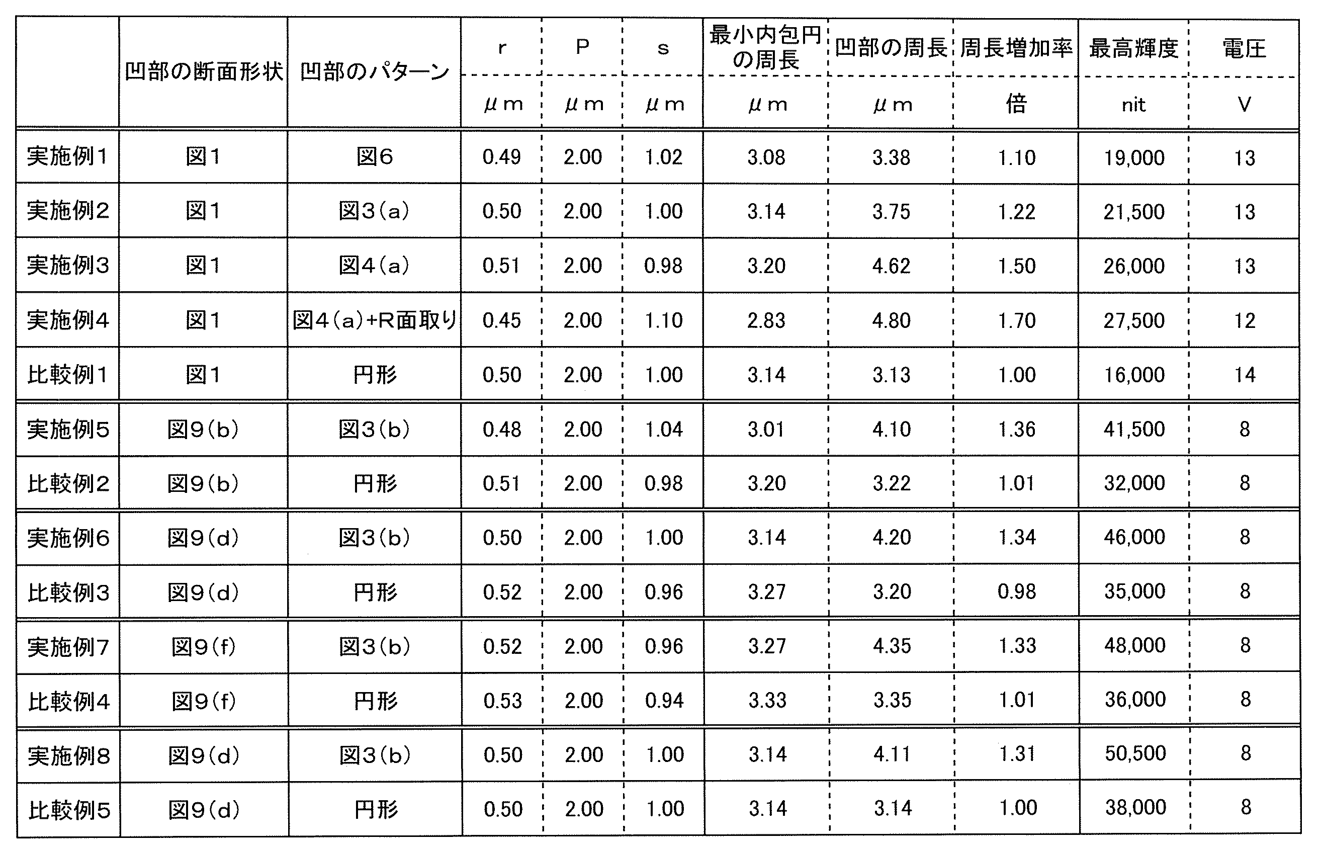
[評価結果]
表1において、凹部16の断面形状が同一である実施例1~4と比較例1、実施例5と比較例2、実施例6と比較例3、実施例7と比較例4、実施例8と比較例5をそれぞれ比較すると、何れも本実施の形態の有機電界発光素子の方が、最高輝度が高いことがわかる。これは凹部16の周長を長くすることで発光部17のエッジ長さを大きくなるため、電流集中を抑制することができ、電流が発光部17の発光部分全体に流れやすくなるためと考えられる。つまりこれにより、電流密度を高くしても電流集中が発生しにくくなるため、発光部17が焼けきれにくくなる。その結果、最高輝度が高くなる。
表1において、凹部16の断面形状が同一である実施例1~4と比較例1、実施例5と比較例2、実施例6と比較例3、実施例7と比較例4、実施例8と比較例5をそれぞれ比較すると、何れも本実施の形態の有機電界発光素子の方が、最高輝度が高いことがわかる。これは凹部16の周長を長くすることで発光部17のエッジ長さを大きくなるため、電流集中を抑制することができ、電流が発光部17の発光部分全体に流れやすくなるためと考えられる。つまりこれにより、電流密度を高くしても電流集中が発生しにくくなるため、発光部17が焼けきれにくくなる。その結果、最高輝度が高くなる。
10…有機電界発光素子、11…基板、12…陽極層、13…誘電体層、14…陰極層、16…凹部、16a…穿孔部、17…発光部、18…第2凹部、21…最小円、200…表示装置、300…照明装置
Claims (9)
- 第1の電極層と、
第2の電極層と、
前記第1の電極層と前記第2の電極層の間に形成される誘電体層と、
少なくとも前記誘電体層を貫通して形成される凹部と、
前記凹部の内面と接触して形成され、電流を供給することで光を発する発光部と、を備え、
前記凹部の前記光の取り出し側から見た形状の周長が、当該形状を内包する最小円の周長より長いことを特徴とする有機電界発光素子。 - 前記形状は、凹多角形形状であることを特徴とする請求項1に記載の有機電界発光素子。
- 前記凹多角形形状は、頂点を8以上有することを特徴とする請求項2に記載の有機電界発光素子。
- 前記形状は、フラクタル構造を有する形状であることを特徴とする請求項1に記載の有機電界発光素子。
- 前記形状を構成する辺の長さは、略同一であることを特徴とする請求項1乃至4の何れか1項に記載の有機電界発光素子。
- 前記形状の頂点部を更に面取りする形状としたことを特徴とする請求項1乃至5の何れか1項に記載の有機電界発光素子。
- 前記第1の電極層を形成するための基板を更に有し、
前記基板は、前記凹部に対応する位置に穿孔部を有することを特徴とする請求項1乃至6の何れか1項に記載の有機電界発光素子。 - 請求項1乃至7の何れか1項に記載の有機電界発光素子を備えることを特徴とする表示装置。
- 請求項1乃至7の何れか1項に記載の有機電界発光素子を備えることを特徴とする照明装置。
Priority Applications (1)
| Application Number | Priority Date | Filing Date | Title |
|---|---|---|---|
| US13/116,900 US20110227107A1 (en) | 2008-11-27 | 2011-05-26 | Light-emitting element, image display device and illuminating device |
Applications Claiming Priority (2)
| Application Number | Priority Date | Filing Date | Title |
|---|---|---|---|
| JP2008-302699 | 2008-11-27 | ||
| JP2008302699 | 2008-11-27 |
Related Parent Applications (1)
| Application Number | Title | Priority Date | Filing Date |
|---|---|---|---|
| PCT/JP2010/058933 Continuation-In-Part WO2011148478A1 (ja) | 2008-11-27 | 2010-05-26 | 発光素子、画像表示装置および照明装置 |
Related Child Applications (1)
| Application Number | Title | Priority Date | Filing Date |
|---|---|---|---|
| US13/116,900 Continuation-In-Part US20110227107A1 (en) | 2008-11-27 | 2011-05-26 | Light-emitting element, image display device and illuminating device |
Publications (1)
| Publication Number | Publication Date |
|---|---|
| WO2010061898A1 true WO2010061898A1 (ja) | 2010-06-03 |
Family
ID=42225769
Family Applications (1)
| Application Number | Title | Priority Date | Filing Date |
|---|---|---|---|
| PCT/JP2009/069975 Ceased WO2010061898A1 (ja) | 2008-11-27 | 2009-11-26 | 有機電界発光素子、表示装置および照明装置 |
Country Status (2)
| Country | Link |
|---|---|
| TW (1) | TW201031262A (ja) |
| WO (1) | WO2010061898A1 (ja) |
Cited By (2)
| Publication number | Priority date | Publication date | Assignee | Title |
|---|---|---|---|---|
| EP2712276A4 (en) * | 2011-05-19 | 2014-11-12 | Showa Denko Kk | ORGANIC LIGHT-EMITTING ELEMENT, METHOD FOR PRODUCING THE ORGANIC LIGHT-EMITTING ELEMENTS, DISPLAY DEVICE AND LIGHTING DEVICE |
| WO2018028605A1 (zh) * | 2016-08-11 | 2018-02-15 | 昆山维信诺科技有限公司 | 有机电致发光器件及其制备方法 |
Families Citing this family (1)
| Publication number | Priority date | Publication date | Assignee | Title |
|---|---|---|---|---|
| US10277194B2 (en) * | 2017-09-15 | 2019-04-30 | Globalfoundries Singapore Pte. Ltd. | Acoustic MEMs resonator and filter with fractal electrode and method for producing the same |
Citations (5)
| Publication number | Priority date | Publication date | Assignee | Title |
|---|---|---|---|---|
| JPH10247588A (ja) * | 1997-03-04 | 1998-09-14 | Idemitsu Kosan Co Ltd | 有機el発光装置 |
| JP2000173777A (ja) * | 1998-12-09 | 2000-06-23 | Futaba Corp | 有機el素子 |
| WO2001006577A1 (en) * | 1999-07-20 | 2001-01-25 | Sri International | Cavity-emission electroluminescent device and method for forming the device |
| JP2002043053A (ja) * | 2000-05-18 | 2002-02-08 | Tohoku Pioneer Corp | 有機エレクトロルミネッセンス表示パネル及び有機エレクトロルミネッセンス表示パネルの製造方法及び多面取り用基板 |
| JP2004133032A (ja) * | 2002-10-08 | 2004-04-30 | Seiko Epson Corp | 微細構造物の製造方法、光学素子、集積回路および電子機器 |
-
2009
- 2009-11-26 WO PCT/JP2009/069975 patent/WO2010061898A1/ja not_active Ceased
- 2009-11-26 TW TW098140366A patent/TW201031262A/zh unknown
Patent Citations (5)
| Publication number | Priority date | Publication date | Assignee | Title |
|---|---|---|---|---|
| JPH10247588A (ja) * | 1997-03-04 | 1998-09-14 | Idemitsu Kosan Co Ltd | 有機el発光装置 |
| JP2000173777A (ja) * | 1998-12-09 | 2000-06-23 | Futaba Corp | 有機el素子 |
| WO2001006577A1 (en) * | 1999-07-20 | 2001-01-25 | Sri International | Cavity-emission electroluminescent device and method for forming the device |
| JP2002043053A (ja) * | 2000-05-18 | 2002-02-08 | Tohoku Pioneer Corp | 有機エレクトロルミネッセンス表示パネル及び有機エレクトロルミネッセンス表示パネルの製造方法及び多面取り用基板 |
| JP2004133032A (ja) * | 2002-10-08 | 2004-04-30 | Seiko Epson Corp | 微細構造物の製造方法、光学素子、集積回路および電子機器 |
Non-Patent Citations (1)
| Title |
|---|
| SMELA, E. ET AL.: "Planar microfabricated polymer light-emitting diodes", SEMICONDUCTOR SCIENCE AND TECHNOLOGY, vol. 13, no. 4, April 1998 (1998-04-01), pages 433 - 439 * |
Cited By (5)
| Publication number | Priority date | Publication date | Assignee | Title |
|---|---|---|---|---|
| EP2712276A4 (en) * | 2011-05-19 | 2014-11-12 | Showa Denko Kk | ORGANIC LIGHT-EMITTING ELEMENT, METHOD FOR PRODUCING THE ORGANIC LIGHT-EMITTING ELEMENTS, DISPLAY DEVICE AND LIGHTING DEVICE |
| WO2018028605A1 (zh) * | 2016-08-11 | 2018-02-15 | 昆山维信诺科技有限公司 | 有机电致发光器件及其制备方法 |
| CN107732019A (zh) * | 2016-08-11 | 2018-02-23 | 昆山维信诺科技有限公司 | 有机电致发光器件及其制备方法 |
| CN107732019B (zh) * | 2016-08-11 | 2019-09-17 | 昆山维信诺科技有限公司 | 有机电致发光器件及其制备方法 |
| US11251382B2 (en) | 2016-08-11 | 2022-02-15 | Suzhou Qingyue Oftoelectronics Technology Co., Ltd. | Organic electroluminescent devices and manufacturing methods thereof |
Also Published As
| Publication number | Publication date |
|---|---|
| TW201031262A (en) | 2010-08-16 |
Similar Documents
| Publication | Publication Date | Title |
|---|---|---|
| JP5523363B2 (ja) | 発光素子、発光素子の製造方法、画像表示装置および照明装置 | |
| JP4913927B1 (ja) | エレクトロルミネッセント素子、表示装置および照明装置 | |
| WO2010016512A1 (ja) | 有機電界発光素子、表示装置および照明装置 | |
| JP4882037B1 (ja) | 有機発光素子および有機発光素子の製造方法 | |
| WO2011081057A1 (ja) | 電界発光素子、電界発光素子の製造方法、表示装置および照明装置 | |
| WO2010067861A1 (ja) | 有機電界発光素子、表示装置および照明装置 | |
| WO2010061898A1 (ja) | 有機電界発光素子、表示装置および照明装置 | |
| WO2010032758A1 (ja) | 有機電界発光素子、表示装置および照明装置 | |
| KR20160094525A (ko) | 유기 발광 소자와 그 제조 방법 및 그를 이용한 유기 발광 디스플레이 장치 | |
| WO2012029156A1 (ja) | El素子、el素子の製造方法、表示装置および照明装置 | |
| WO2011148478A1 (ja) | 発光素子、画像表示装置および照明装置 | |
| WO2011043210A1 (ja) | 電界発光素子、電界発光素子の製造方法、表示装置および照明装置 | |
| US20110227107A1 (en) | Light-emitting element, image display device and illuminating device | |
| WO2010032757A1 (ja) | 有機電界発光素子、表示装置および照明装置 | |
| WO2012147390A1 (ja) | 有機発光素子、有機発光素子の製造方法、表示装置および照明装置 | |
| JP5255161B1 (ja) | 有機発光素子、有機発光素子の製造方法、表示装置および照明装置 | |
| JP2011081948A (ja) | 有機電界発光素子、有機電界発光素子の製造方法、表示装置および照明装置 | |
| JP2012243517A (ja) | 有機発光素子、有機発光素子の製造方法、表示装置および照明装置 | |
| JP5553625B2 (ja) | 電界発光素子、表示装置および照明装置 |
Legal Events
| Date | Code | Title | Description |
|---|---|---|---|
| 121 | Ep: the epo has been informed by wipo that ep was designated in this application |
Ref document number: 09829143 Country of ref document: EP Kind code of ref document: A1 |
|
| NENP | Non-entry into the national phase |
Ref country code: DE |
|
| NENP | Non-entry into the national phase |
Ref country code: JP |
|
| 122 | Ep: pct application non-entry in european phase |
Ref document number: 09829143 Country of ref document: EP Kind code of ref document: A1 |