WO2010061492A1 - 表示モジュール - Google Patents
表示モジュール Download PDFInfo
- Publication number
- WO2010061492A1 WO2010061492A1 PCT/JP2009/003068 JP2009003068W WO2010061492A1 WO 2010061492 A1 WO2010061492 A1 WO 2010061492A1 JP 2009003068 W JP2009003068 W JP 2009003068W WO 2010061492 A1 WO2010061492 A1 WO 2010061492A1
- Authority
- WO
- WIPO (PCT)
- Prior art keywords
- flexible printed
- frame member
- display module
- circuit board
- printed circuit
- Prior art date
- Legal status (The legal status is an assumption and is not a legal conclusion. Google has not performed a legal analysis and makes no representation as to the accuracy of the status listed.)
- Ceased
Links
Images





Classifications
-
- G—PHYSICS
- G02—OPTICS
- G02F—OPTICAL DEVICES OR ARRANGEMENTS FOR THE CONTROL OF LIGHT BY MODIFICATION OF THE OPTICAL PROPERTIES OF THE MEDIA OF THE ELEMENTS INVOLVED THEREIN; NON-LINEAR OPTICS; FREQUENCY-CHANGING OF LIGHT; OPTICAL LOGIC ELEMENTS; OPTICAL ANALOGUE/DIGITAL CONVERTERS
- G02F1/00—Devices or arrangements for the control of the intensity, colour, phase, polarisation or direction of light arriving from an independent light source, e.g. switching, gating or modulating; Non-linear optics
- G02F1/01—Devices or arrangements for the control of the intensity, colour, phase, polarisation or direction of light arriving from an independent light source, e.g. switching, gating or modulating; Non-linear optics for the control of the intensity, phase, polarisation or colour
- G02F1/13—Devices or arrangements for the control of the intensity, colour, phase, polarisation or direction of light arriving from an independent light source, e.g. switching, gating or modulating; Non-linear optics for the control of the intensity, phase, polarisation or colour based on liquid crystals, e.g. single liquid crystal display cells
- G02F1/133—Constructional arrangements; Operation of liquid crystal cells; Circuit arrangements
- G02F1/1333—Constructional arrangements; Manufacturing methods
- G02F1/1345—Conductors connecting electrodes to cell terminals
- G02F1/13452—Conductors connecting driver circuitry and terminals of panels
-
- G—PHYSICS
- G02—OPTICS
- G02F—OPTICAL DEVICES OR ARRANGEMENTS FOR THE CONTROL OF LIGHT BY MODIFICATION OF THE OPTICAL PROPERTIES OF THE MEDIA OF THE ELEMENTS INVOLVED THEREIN; NON-LINEAR OPTICS; FREQUENCY-CHANGING OF LIGHT; OPTICAL LOGIC ELEMENTS; OPTICAL ANALOGUE/DIGITAL CONVERTERS
- G02F1/00—Devices or arrangements for the control of the intensity, colour, phase, polarisation or direction of light arriving from an independent light source, e.g. switching, gating or modulating; Non-linear optics
- G02F1/01—Devices or arrangements for the control of the intensity, colour, phase, polarisation or direction of light arriving from an independent light source, e.g. switching, gating or modulating; Non-linear optics for the control of the intensity, phase, polarisation or colour
- G02F1/13—Devices or arrangements for the control of the intensity, colour, phase, polarisation or direction of light arriving from an independent light source, e.g. switching, gating or modulating; Non-linear optics for the control of the intensity, phase, polarisation or colour based on liquid crystals, e.g. single liquid crystal display cells
- G02F1/133—Constructional arrangements; Operation of liquid crystal cells; Circuit arrangements
- G02F1/1333—Constructional arrangements; Manufacturing methods
- G02F1/133308—Support structures for LCD panels, e.g. frames or bezels
Definitions
- the present invention relates to a display module, and more particularly to a display module including a flexible printed circuit board.
- This liquid crystal display module generally includes a pair of substrates (that is, a TFT (Thin Film Transistor) substrate and a CF (Color Filter) substrate) disposed opposite to each other and a liquid crystal layer provided between the pair of substrates. And a backlight unit provided below the liquid crystal display panel.
- a pair of substrates that is, a TFT (Thin Film Transistor) substrate and a CF (Color Filter) substrate
- CF Color Filter
- a flexible printed circuit board is used to cope with the thinning and miniaturization of the liquid crystal display module.
- the flexible printed wiring board is connected to the TFT substrate of the liquid crystal display module, and a plurality of elements are provided on the surface thereof.
- the flexible printed circuit board is formed by being pulled out from the end portion of the liquid crystal display panel, the flexible printed circuit board is bent to the inside of the liquid crystal display module in order to cope with a reduction in thickness and size. Need to be fixed.
- a fixing structure of this flexible printed circuit board for example, there is a structure in which the fixing unit such as an adhesive tape is adhered and fixed to the surface of the back side of the backlight unit (that is, the non-display side of the liquid crystal display module). It is disclosed (for example, see Patent Document 1). Further, a structure is disclosed in which a fixing rib having a claw shape is provided on the flexible printed board, and the fixing rib is attached and fixed to a component to which the flexible printed board is fixed (for example, Patent Document 2). reference).
- the present invention has been made in view of the above-described problems, and provides a display module that can securely fix a flexible printed circuit board without impairing reworkability, and can cope with a reduction in thickness and size.
- the purpose is to do.
- a display module includes a display panel and a flexible printed circuit board connected to the display panel, and fixes the flexible printed circuit board by pressing the folded flexible printed circuit board. It is characterized by providing the fixing member for doing.
- the flexible printed circuit board can be securely fixed without causing the inconvenience that the tape is peeled off due to the repulsive force of the folded flexible printed circuit board. Become. Further, as compared with the conventional fixing structure using a tape, the fixed state of the flexible printed board can be easily released, so that the reworkability is improved. In addition, unlike the conventional fixing structure using ribs, an increase in the external dimensions of the display module can be prevented, so that an increase in the size of the display module can be prevented. Therefore, it becomes possible to cope with the reduction in thickness and size of the display module.
- the display module according to the present invention may further include a frame member that holds the display panel, and the frame member may also serve as a fixing member.
- the frame member also serves as a fixing member, the flexible printed board can be reliably fixed without increasing the number of parts.
- the display module according to the present invention may further include a frame member that holds the display panel, and the frame member and the fixing member may be integrally formed.
- an opening for exposing the terminal portion of the flexible printed board may be formed in the fixing member.
- the fixing member may be formed of metal or resin.
- the fixing member can be formed from an inexpensive and versatile material.
- the display module according to the present invention has an excellent characteristic that the flexible printed circuit board can be securely fixed, the entire module can be reduced in thickness and weight, and reworkability can be improved. ing. Therefore, the display panel is preferably used for a display module using a liquid crystal display panel.
- the folded flexible printed circuit board can be securely fixed in the display module including the flexible printed circuit board. Further, the entire module can be reduced in thickness and weight. Furthermore, the reworkability of the flexible printed circuit board can be improved.
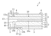
- FIG. 1 is an exploded perspective view of a display module according to the first embodiment of the present invention
- FIG. 2 is a cross-sectional view of the display module according to the first embodiment of the present invention.
- a liquid crystal display module will be described as an example of the display module.
- the liquid crystal display module 1 is disposed on the liquid crystal display panel 2 and the back side of the liquid crystal panel 2 (that is, the opposite side of the liquid crystal display panel 1). And a backlight unit 3 for supplying light. That is, the liquid crystal display module 1 of the present embodiment is a transmissive liquid crystal display module that selectively transmits light from the backlight unit 3 to the liquid crystal display panel 2 and performs transmissive display. Installed in equipment.
- the liquid crystal display module 1 includes an upper frame member 4 and a lower frame member 5, and the liquid crystal panel 2 and the backlight unit 3 include the upper frame member 4 and the lower frame member 5.
- the side frame member 5 is arranged inside.
- the liquid crystal display panel 2 includes a TFT substrate 6 on which a plurality of thin film transistors (TFTs) serving as switching elements are formed, and a CF substrate 7 disposed opposite to the TFT substrate 6. And a liquid crystal layer (not shown) provided between the TFT substrate 6 and the CF substrate 7.
- TFT substrate 6 and the CF substrate 7 are each formed in a rectangular plate shape.
- the TFT substrate 6 is disposed on the backlight unit 3 side (that is, the non-display side of the liquid crystal display panel 1), and the CF substrate 7 is disposed on the display side of the liquid crystal display panel 1.
- the first polarizing plate 8 is provided on the surface of the TFT substrate 6 on the backlight unit 3 side, and the second polarizing plate 9 is provided on the display side surface of the liquid crystal display panel 1 of the CF substrate 7. It has been.
- the TFT substrate 6 includes a plurality of gate lines (not shown) provided so as to extend in parallel with each other on a substrate body such as a glass substrate or a plastic substrate, and a gate insulating film provided so as to cover each gate line. (Not shown).
- the TFT substrate 6 includes a plurality of source lines (not shown) provided on the gate insulating film so as to extend in parallel to each other in a direction orthogonal to the gate lines, and each gate line and each intersection of the source lines. That is, a plurality of TFTs (not shown) provided for each pixel are provided.
- the TFT substrate 6 includes an interlayer insulating film provided so as to cover each TFT and each source line, and a plurality of pixel electrodes (not shown) provided in a matrix on the interlayer insulating film and connected to each TFT. And an alignment film (not shown) provided to cover each pixel electrode.
- the CF substrate 7 is, for example, a black matrix (not shown) provided in a grid shape and a frame shape as a light-shielding portion on a substrate body such as a glass substrate or a plastic substrate, and a red color provided between each grid of the black matrix. And a color filter (not shown) including a green layer, a green layer, and the like.
- the CF substrate 7 covers a common electrode (not shown) provided so as to cover the black matrix and the color filter, a photo spacer (not shown) provided in a column shape on the common electrode, and a common electrode. And an alignment film (not shown) provided.
- the first polarizing plate 8 has a light absorption anisotropy by adsorbing or dyeing a dichroic dye such as iodine or a dye on a polyvinyl alcohol (PVA) film or the like, uniaxially stretching and orienting with high accuracy. What was used was used as the base material.
- PVA polyvinyl alcohol
- the polyvinyl alcohol film itself has a problem in terms of hygroscopicity and strength, it is usually used in a state of being sandwiched and protected by a cellulose triacetate (TAC) film having high transparency and excellent optical characteristics.
- TAC cellulose triacetate
- the second polarizing plate 9 adsorbs or dyes a dichroic dye such as iodine or a dye on a polyvinyl alcohol (PVA) film or the like, and uniaxially stretches and orients it with high accuracy. Those having light absorption anisotropy are used as the base material.
- a dichroic dye such as iodine or a dye on a polyvinyl alcohol (PVA) film or the like
- the first polarizing plate 8 and the second polarizing plate 9 are configured to sandwich the liquid crystal layer so that the polarization directions thereof are orthogonal or parallel to each other.
- the liquid crystal layer is made of, for example, a nematic liquid crystal material having electro-optical characteristics.
- the TFT substrate 6 is formed with a display area 10 that contributes to display and a frame area 11 that is formed around the display area 10 and does not contribute to display.
- a circuit component 12 for controlling driving of the liquid crystal display module 1 is mounted on the frame region 11 of the TFT substrate 6, and a flexible printed circuit board 13 for supplying a signal to the circuit component 12 is connected. ing. That is, the flexible printed circuit board 13 has one end 13 a connected to a terminal on which the circuit component 12 of the TFT substrate 6 is mounted.
- the other end 13b of the flexible printed circuit board 13 is bent toward the lower backlight unit 3 side. And the other end part 13b of the flexible printed circuit board 13 becomes a structure arrange
- an LED 14 and a circuit component 40 which are light sources of the backlight unit 3 are provided on the surface of the flexible printed circuit board 13 on the backlight unit 3 side.
- the flexible printed circuit board 13 is formed with terminal portions 15 connected to an external board (not shown).
- a polyimide resin or the like having a high heat resistance and a flexible polymer film laminated with a conductor circuit layer made of copper foil can be used.
- the backlight unit 3 includes a light guide plate (light emitting light guide member) 16, a lens sheet 17 provided on the surface of the light guide plate 16 (that is, the emission surface 16 a of the light guide plate 16), and the back surface of the light guide plate 16 (that is, The reflection sheet 20 is provided on the surface opposite to the emission surface 16a.
- the backlight unit 3 constitutes a sidelight type backlight unit.
- the light guide plate 16 is disposed on the back side of the TFT substrate 6 so as to face the TFT substrate 2 as shown in FIG.
- the exit surface 16 a of the light guide plate 16 faces the TFT substrate 6, and the entrance surface 16 b is configured by one of the four side surfaces of the light guide plate 16.
- transparent resin materials such as an acrylic resin, a polycarbonate, an epoxy resin, glass, etc. can be mentioned.
- the LED 14 is held by the upper frame member 4 and the lower frame member 5 with the flexible printed circuit board 13 bent so that the LED 14 faces the incident surface 16 b of the light guide plate 16. Yes. That is, the LED 14 is arranged inside the upper frame member 4 and the lower frame member 5 together with the circuit component 12. The light emitted from the LED 14 enters the light guide plate 16 from the incident surface 16b, and the light guide plate 16 diffuses the light of the LED 14 incident from the incident surface 16b and emits the light from the output surface 16a. ing.
- the lens sheet 17 is provided on the surface of the light guide plate 16 so that light from the light guide plate 16 enters.
- the lens sheet 17 is configured by forming a plurality of cones made of acrylic resin, polycarbonate, or the like on a base made of polyester film, polyethylene terephthalate film (PET film), or the like.
- the lens sheet 17 is provided such that the top of the cone-shaped body faces in the direction opposite to the light guide plate 16 side (that is, faces the liquid crystal panel 2 side).
- the lens sheet 17 is formed with a thickness in the range of 150 to 300 ⁇ m, for example, and the height of the cone is formed with a thickness of 10 to 45 ⁇ m, for example.
- the lens sheet 17 may be formed with uneven surfaces alternately arranged along the width direction of the light guide plate 16, or triangular prism-like prism surfaces arranged along the width direction of the light guide plate 16. It may be formed.
- the reflection sheet 20 is provided on the back surface of the light guide plate 16 so as to be substantially horizontal.
- the reflection sheet 20 is configured by a white diffusion sheet having no directivity, a light diffusion sheet having directivity by randomly arranging minute uneven shapes.
- the reflection sheet 20 is formed of a multilayer plastic film having a white diffuse reflection layer or a metal vapor deposition reflection layer on the surface thereof.
- a multilayer plastic film for example, a multilayer laminate film of polyethylene naphthalate (PEN) and its copolymer (coPEN), or a laminate of PEN and syndiotactic potastyrene (sPS) is used.
- sPS syndiotactic potastyrene
- an adhesive or a double-sided tape can be used.
- the reflection sheet 20 has a thickness in the range of 15 to 200 ⁇ m, for example.
- the reflection sheet 20 may be provided obliquely on the back surface of the light guide plate 16.
- the upper frame member 4 is made of, for example, a metal such as SUS or a resin such as polycarbonate, and is formed in a substantially rectangular frame shape. Further, on the side surface 4 a of the upper frame member 4, a locking piece 21 for contacting the side surface 5 a of the lower frame member 5 and locking the lower frame member 5 is formed.
- the lower frame 5 member is made of, for example, a metal such as SUS, or a resin such as polycarbonate, and has a substantially rectangular shape. Further, an insertion hole 22 for inserting a locking piece 21 formed on the side surface 4 a of the upper frame member 4 is formed on the side surface 5 a of the lower frame member 5.
- the liquid crystal display panel 2 and the backlight unit 3 are sandwiched between the upper frame member 4 and the lower frame member 5.
- the lower frame member 5 is locked to the upper frame member 4 by inserting the locking pieces 21 formed on the upper frame member 4 into the insertion holes 22 formed in the lower frame member 5. At this time, the liquid crystal panel 2 and the backlight unit 3 are held by the upper frame member 4 and the lower frame member 5.
- a transmissive display is performed by turning on the LED 14 provided on the side of the backlight unit 5.
- the emitted light is introduced into the light guide plate 16 via the incident surface 16 b of the light guide plate 16, and the light introduced into the light guide plate 16 propagates inside while being reflected by the inner surface of the light guide plate 16.
- a part of the propagation light inside the light guide plate 16 is emitted from the emission surface 16 a of the light guide plate 16.
- the other propagation light inside the light guide plate 16 is emitted from the lower surface of the light guide plate 16 and scattered and reflected by the reflection sheet 20.
- the reflected light passes through the light guide plate 16 and is emitted from the emission surface 16 a of the light guide plate 16.
- the light emitted from the emission surface 16a of the light guide plate 16 is transmitted through the lens sheet 17, and the directivity is controlled, and is collected on the TFT substrate 6 of the liquid crystal display panel 2, and the TFT substrate 2 is moved from the back side. Exposure. In this way, the display area 10 of the TFT substrate 6 is illuminated from the back side, whereby an image is displayed on the display area of the liquid crystal display panel 2.
- the flexible printed circuit board 13 bent to the backlight unit 3 side is fixed by being pressed by the lower frame member 5. That is, the lower frame member 5 is used as a fixing member for fixing the flexible printed circuit board 13 by pressing the folded flexible printed circuit board 13.
- the flexible printed circuit board 13 can be securely fixed without causing the inconvenience that the tape peels off due to the repulsive force of the flexible printed circuit board 13. .
- the fixed state of the flexible printed board 13 can be easily released, so that the reworkability can be improved.
- an increase in the external dimension of the liquid crystal display module 1 can be prevented, so that an increase in the size of the liquid crystal display module 1 can be prevented.
- the lower frame member 5 also serves as a fixing member for fixing the flexible printed circuit board 13, unlike the conventional tape fixing structure and rib fixing structure, the flexible printed circuit board does not increase the number of parts. 13 can be securely fixed.
- the lower frame member 5 is formed with an opening 23 for exposing the terminal portion 15 of the flexible printed circuit board 13 when the flexible printed circuit board 13 is fixed. . With such a configuration, even when the flexible printed board 13 is fixed by the lower frame member 5, the flexible printed board 13 and the external board can be reliably connected via the terminal portion 15.
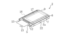
- 3 to 5 are perspective views for explaining a method of assembling the display module according to the present embodiment.
- the liquid crystal display panel 2 is placed on the surface of the backlight unit 3, and the liquid crystal display panel 2 and the backlight unit 3 are overlapped.
- the flexible printed circuit board 13 is bent toward the backlight unit 3 side.
- the liquid crystal display panel 2 and the backlight unit 3 are sandwiched between the upper frame member 4 and the lower frame member 5.
- the lower frame member 5 is locked to the upper frame member 4 by inserting the locking pieces 21 formed on the upper frame member 4 into the insertion holes 22 formed in the lower frame member 5.
- the liquid crystal display panel 2 and the backlight unit 3 are held by the upper frame member 4 and the lower frame member 5.
- the flexible printed circuit board 13 is fixed by the lower frame member 5, and the terminal portion 15 of the flexible printed circuit board 13 is exposed to the outside through the opening 23 formed in the lower frame member 5.
- the liquid crystal display module 1 shown in FIG. 2 is assembled.
- the lower frame member 5 is used as a fixing member for fixing the flexible printed circuit board 13 by pressing the folded flexible printed circuit board 13. Therefore, the flexible printed circuit board 13 can be securely fixed without causing the disadvantage that the tape peels off due to the repulsive force of the folded flexible printed circuit board 13.
- the lower frame member 5 also serves as a fixing member. Therefore, the flexible printed circuit board 13 can be securely fixed without increasing the number of parts.
- the opening 23 for exposing the terminal portion 15 of the flexible printed circuit board 13 is formed in the lower frame member 5. Therefore, even when the flexible printed board 13 is fixed by the lower frame member 5, the terminal portion 15 of the flexible printed board 13 and the external board can be reliably connected.
- the lower frame member 5 which is a fixing member is formed of a metal such as SUS or a resin such as polycarbonate. Therefore, the fixing member can be formed of an inexpensive and versatile material.
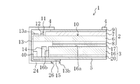
- FIG. 6 is an exploded perspective view of a display module according to the second embodiment of the present invention
- FIG. 7 is a cross-sectional view of the display module according to the second embodiment of the present invention. Note that the same components as those in the first embodiment are denoted by the same reference numerals, and description thereof is omitted. Also in this embodiment, a liquid crystal display module will be described as an example of the display module.
- This embodiment is characterized in that the flexible printed circuit board 13 bent toward the backlight unit 3 is pressed and fixed by a fixing member formed on the upper frame member 4.
- the upper frame member 4 is a pressing portion that is a fixing member for pressing and fixing the flexible printed circuit board 13 bent toward the backlight unit 3 side. 24 is formed.
- the pressing portion 24 is formed of a metal such as SUS constituting the upper frame member 4 or a resin such as polycarbonate, and the upper frame member 4 and the pressing portion 24 are integrally formed.
- the pressing unit 24 fixes the flexible printed circuit board 13 by pressing the surface of the flexible printed circuit board 13 bent toward the backlight unit 3 side.
- the flexible printed circuit board 13 can be securely fixed without causing the inconvenience of peeling off the tape.
- the release of the fixed state of the flexible printed circuit board 13 becomes easy, reworkability improves.
- an increase in the external dimension of the liquid crystal display module 1 can be prevented, an increase in the size of the liquid crystal display module 1 can be prevented.
- the pressing portion 24 formed on the upper frame member 4 has an opening for exposing the terminal portion 15 of the flexible printed circuit board 13 when the flexible printed circuit board 13 is fixed. 26 is formed.
- FIGS. 8 to 11 are perspective views for explaining a method of assembling the display module according to the present embodiment.
- the liquid crystal display panel 2 is placed on the surface of the backlight unit 3, and the liquid crystal display panel 2, the backlight unit 3, and the lower frame member 5 are overlapped.
- the flexible printed board 13 is bent toward the backlight unit 3 side.
- the upper frame member 4 is slid in the direction of the arrow in the drawing from the flexible printed circuit board 13 side, and the liquid crystal panel 2 and the backlight unit 3 are moved as shown in FIG. It is sandwiched between the upper frame member 4 and the lower frame member 5.
- the locking piece 21 formed on the upper frame member 4 is inserted into the insertion hole 22 formed on the lower frame member 5.
- the lower frame member 5 is locked to the upper frame member 4, and the liquid crystal panel 2 and the backlight unit 3 are held by the upper frame member 4 and the lower frame member 5.
- the flexible printed circuit board 13 is fixed by the pressing portion 24 of the upper frame member 4, and the terminal portion 15 of the flexible printed circuit board 13 is exposed to the outside through the opening 26 formed in the upper frame member 5. Exposed.
- the liquid crystal display module 1 shown in FIG. 7 is assembled.
- the upper frame member 4 and the pressing portion 24 that is a fixing member are integrally formed. Accordingly, the manufacturing efficiency of the fixing member is improved, and the flexible printed board 13 can be reliably fixed with a simple configuration.
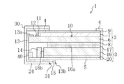
- the flexible printed circuit board 13 is fixed by the upper frame member 4 or the lower frame member 5, but by pressing the folded flexible printed circuit board 13 as shown in FIGS.
- the fixing member 30 for fixing the flexible printed circuit board 13 may be provided separately. That is, the fixing member 30 may be provided separately from the upper frame member 4 and the lower frame member 5. As shown in FIGS. 12 and 13, the fixing member 30 may be formed with an opening 31 for exposing the terminal portion 15 of the flexible printed circuit board 13 when the flexible printed circuit board 13 is fixed. .
- the fixing member 30 is formed of, for example, a metal such as SUS or a resin such as polycarbonate, like the upper frame member 4 and the lower frame member 5 described above. With such a configuration, the same effects as in the above (1) to (3) and (5) to (6) can be obtained.
- the liquid crystal display module has been described as an example of the display module, but the present invention is not limited to this.
- the present invention can be applied to a light emitting element display module using a light emitting element such as an organic EL (Electro Luminescence) that includes a flexible printed circuit board and does not employ a backlight system.
- a light emitting element such as an organic EL (Electro Luminescence) that includes a flexible printed circuit board and does not employ a backlight system.
- the present invention is suitable for a display module including a flexible printed board.
Landscapes
- Physics & Mathematics (AREA)
- Nonlinear Science (AREA)
- Mathematical Physics (AREA)
- Chemical & Material Sciences (AREA)
- Crystallography & Structural Chemistry (AREA)
- General Physics & Mathematics (AREA)
- Optics & Photonics (AREA)
- Liquid Crystal (AREA)
- Devices For Indicating Variable Information By Combining Individual Elements (AREA)
Abstract
液晶表示モジュール(1)は、液晶表示パネル(2)と、液晶表示パネル(2)に接続されたフレキシブルプリント基板(13)と、液晶表示パネル(2)を支持する上側フレーム部材(4)及び下側フレーム部材(5)とを備えている。そして、下側フレーム部材(5)は、折り曲げられたフレキシブルプリント基板(13)を押圧することにより、フレキシブルプリント基板(13)を固定する。
Description
本発明は、表示モジュールに関し、特に、フレキシブルプリント基板を備える表示モジュールに関する。
近年、ノートパソコンや携帯電話機等の表示パネルを備える電子機器の急速なモバイル化等に伴い、液晶表示モジュール等の表示モジュールに対して、更なる薄型化及び小型化が望まれている。
この液晶表示モジュールは、一般に、互いに対向して配置された一対の基板(即ち、TFT(Thin Film Transistor)基板とCF(Color Filter)基板)及び一対の基板の間に設けられた液晶層とを有する液晶表示パネルと、当該液晶表示パネルの下方に設けられたバックライトユニットとを備えている。
また、液晶表示モジュールの薄型化及び小型化に対応すべく、フレキシブルプリント基板が使用されている。このフレキシブルプリント配線板は、液晶表示モジュールのTFT基板に接続されるとともに、その表面に複数の素子が設けられている。
ここで、一般に、フレキシブルプリント基板は、液晶表示パネルの端部から外側へ引き出されて形成されているため、薄型化や小型化に対応すべく、フレキシブルプリント基板を液晶表示モジュールの内側へ折り曲げて固定する必要がある。そして、このフレキシブルプリント基板の固定構造として、例えば、バックライトユニットの裏面側(即ち、液晶表示モジュールの反表示側)の表面に、粘着テープ等の固定用のテープにより接着して固定する構造が開示されている(例えば、特許文献1参照)。また、フレキシブルプリント基板に爪形状を有する固定用のリブを設けるとともに、当該固定用のリブを、フレキシブルプリント基板が固定される部品に取り付けて固定する構造が開示されている(例えば、特許文献2参照)。
しかし、上記特許文献1に記載の固定用のテープにより固定構造では、テープによる接着力が低下して、フレキシブルプリント基板の反発力(即ち、折り曲げられたフレキシブルプリント基板が、元の状態に戻ろうとする復元力)により、テープが剥がれてしまい、フレキシブルプリント基板が固定できなくなるという不都合があった。また、テープによる接着力の低下を防止すべく、テープの接着力を強固にすると、フレキシブルプリント基板の固定状態の解除(リワーク)が困難になるという問題があった。
また、上記特許文献2に記載のリブによる固定構造では、液晶表示モジュールの外形寸法が増加するため、液晶表示モジュールのサイズが大きくなってしまい、液晶表示モジュールの薄型化及び小型化に対応することが困難になるという問題があった。
そこで、本発明は、上述の問題に鑑みてなされたものであり、リワーク性を損なうことなく、フレキシブルプリント基板を確実に固定することができるとともに、薄型化及び小型化に対応できる表示モジュールを提供することを目的とする。
上記目的を達成するために、本発明に係る表示モジュールは、表示パネルと、表示パネルに接続されたフレキシブルプリント基板とを備え、折り曲げられたフレキシブルプリント基板を押圧することにより、フレキシブルプリント基板を固定するための固定部材を備えることを特徴とする。
同構成によれば、上記従来のテープによる固定構造とは異なり、折り曲げられたフレキシブルプリント基板の反発力により、テープが剥がれるという不都合を生じることなく、フレキシブルプリント基板を確実に固定することが可能になる。また、上記従来のテープによる固定構造に比し、フレキシブルプリント基板の固定状態の解除が容易になるため、リワーク性が向上する。また、上記従来のリブによる固定構造とは異なり、表示モジュールの外形寸法の増加を防止することができるため、表示モジュールのサイズの増大を防止できる。従って、表示モジュールの薄型化及び小型化に対応することが可能になる。
また、本発明に係る表示モジュールは、表示パネルを保持するフレーム部材を更に備え、フレーム部材が固定部材を兼用しても良い。
同構成によれば、フレーム部材が固定部材を兼用するため、部品点数を増加することなく、フレキシブルプリント基板を確実に固定することが可能になる。
また、本発明に係る表示モジュールは、表示パネルを保持するフレーム部材を更に備え、フレーム部材と固定部材とが一体的に形成されていても良い。
同構成によれば、フレーム部材と固定部材とが一体的に形成されているため、固定部材の製造効率が良好になるとともに、簡単な構成で、フレキシブルプリント基板を確実に固定することが可能になる。
また、本発明に係る表示モジュールは、固定部材に、フレキシブルプリント基板の端子部を露出するための開口部が形成されていても良い。
同構成によれば、固定部材により、フレキシブルプリント基板を固定した場合であっても、フレキシブルプリント基板の端子部と外部基板とを確実に接続することができる。
更に、本発明に係る表示モジュールは、固定部材が、金属、または樹脂により形成されていても良い。
同構成によれば、安価かつ汎用性のある材料により、固定部材を形成することが可能になる。
また、本発明に係る表示モジュールは、フレキシブルプリント基板を確実に固定して、モジュール全体の薄型化、及び軽量化を図ることができるとともに、リワーク性を向上させることができるという優れた特性を備えている。従って、表示パネルに、液晶表示パネルを使用した表示モジュールに好適に使用される。
本発明によれば、フレキシブルプリント基板を備える表示モジュールにおいて、折り曲げられたフレキシブルプリント基板を確実に固定することができる。また、モジュール全体の薄型化、及び軽量化を図ることができる。さらに、フレキシブルプリント基板のリワーク性を向上させることができる。
以下、本発明の実施形態を図面に基づいて詳細に説明する。尚、本発明は、以下の実施形態に限定されるものではない。
(第1の実施形態)
図1は、本発明の第1の実施形態に係る表示モジュールの分解斜視図であり、図2は、本発明の第1の実施形態に係る表示モジュールの断面図である。なお、本実施形態においては、表示モジュールとして、液晶表示モジュールを例に挙げて説明する。
図1は、本発明の第1の実施形態に係る表示モジュールの分解斜視図であり、図2は、本発明の第1の実施形態に係る表示モジュールの断面図である。なお、本実施形態においては、表示モジュールとして、液晶表示モジュールを例に挙げて説明する。
図1、図2に示すように、液晶表示モジュール1は、液晶表示パネル2と、当該液晶パネル2の裏面側(即ち、液晶表示パネル1の反表示側)に配置され、液晶表示パネル2に光を供給するためのバックライトユニット3とを備えている。即ち、本実施形態の液晶表示モジュール1は、バックライトユニット3の光を液晶表示パネル2に選択的に透過させて透過表示を行う透過型の液晶表示モジュールであり、例えば、携帯電話等のモバイル機器に搭載される。
また、図1、図2に示すように、液晶表示モジュール1は、上側フレーム部材4と下側フレーム部材5とを備えており、液晶パネル2及びバックライトユニット3は、上側フレーム部材4と下側フレーム部材5の内部に配置される構成となっている。
液晶表示パネル2は、図1、図2に示すように、スイッチング素子であるTFT(Thin-Film Transistor)が複数形成されたTFT基板6と、TFT基板6に対向して配置されたCF基板7と、TFT基板6及びCF基板7の間に設けられた液晶層(図示省略)とを備えている。なお、TFT基板6及びCF基板7は、それぞれ矩形板状に形成されている。
また、TFT基板6はバックライトユニット3側(即ち、液晶表示パネル1の反表示側)に配置され、CF基板7は液晶表示パネル1の表示側に配置されている。また、TFT基板6のバックライトユニット3側の表面には、第1偏光板8が設けられており、CF基板7の液晶表示パネル1の表示側の表面には、第2偏光板9が設けられている。
TFT基板6は、例えば、ガラス基板やプラスチック基板等の基板本体上に互いに平行に延びるように設けられた複数のゲート線(不図示)と、各ゲート線を覆うように設けられたゲート絶縁膜(不図示)とを備えている。また、TFT基板6は、ゲート絶縁膜上に各ゲート線と直交する方向に互いに平行に延びるように設けられた複数のソース線(不図示)と、各ゲート線及び各ソース線の交差部分毎、すなわち、各画素毎にそれぞれ設けられた複数のTFT(不図示)とを備えている。更に、TFT基板6は、各TFT及び各ソース線を覆うように設けられた層間絶縁膜と、層間絶縁膜上にマトリクス状に設けられ、各TFTに接続された複数の画素電極(不図示)と、各画素電極を覆うように設けられた配向膜(不図示)とを備えている。
CF基板7は、例えば、ガラス基板やプラスチック基板等の基板本体上に格子状及び遮光部として枠状に設けられたブラックマトリクス(不図示)と、ブラックマトリクスの各格子間にそれぞれ設けられた赤色層、緑色層及び青色層などを含むカラーフィルタ(不図示)とを備えている。また、CF基板7は、ブラックマトリクス及びカラーフィルタを覆うように設けられた共通電極(不図示)と、共通電極上に柱状に設けられたフォトスペーサ(不図示)と、共通電極を覆うように設けられた配向膜(不図示)とを備えている。
第1偏光板8は、ポリビニルアルコール(PVA)フィルム等に、ヨウ素や染料などの二色性色素を吸着あるいは染色させ、高精度に一軸延伸し、配向させることによって光の吸収異方性を持たせたものが、その基材として用いられる。なお、ポリビニルアルコールフィルム自身は、吸湿性や強度の点で問題があるため、通常、透明性が高く、光学特性に優れた三酢酸セルロース(TAC)フィルムで挟み込んで保護した状態で用いられる。
第2偏光板9は、第1偏光板8と同様に、ポリビニルアルコール(PVA)フィルム等に、ヨウ素や染料などの二色性色素を吸着あるいは染色させ、高精度に一軸延伸し、配向させることによって光の吸収異方性を持たせたものが、その基材として用いられる。
また、第1偏光板8及び第2偏光板9は、各々の偏光方向が直交又は平行となるようにして、液晶層を挟むように構成されている。なお、液晶層は、例えば、電気光学特性を有するネマチックの液晶材料などにより構成されている。
また、TFT基板6には、表示に寄与する表示領域10と、表示領域10の周りに形成されて表示に寄与しない額縁領域11とが形成されている。そして、TFT基板6の額縁領域11には、液晶表示モジュール1の駆動を制御するための回路部品12が搭載されるとともに、当該回路部品12に信号を供給するためのフレキシブルプリント基板13が接続されている。即ち、フレキシブルプリント基板13は、その一端部13aがTFT基板6の回路部品12が実装された端子に接続されている。
また、図2に示すように、フレキシブルプリント基板13は、その他端部13bが下方のバックライトユニット3側に折り曲げられている。そして、フレキシブルプリント基板13の他端部13bは、後述する反射シート20の下面に配置される構成となっている。また、フレキシブルプリント基板13のバックライトユニット3側の表面には、バックライトユニット3の光源となるLED14と回路部品40とが設けられている。なお、LED14の代わりに、電球等の他の点状の光源、または蛍光管等の線状の光源を用いてもよい。また、フレキシブルプリント基板13には、外部基板(不図示)に接続される端子部15が形成されている。フレキシブルプリント基板13としては、例えば、ポリイミド樹脂等の耐熱性が高く、フレキシブルなポリマーフィルムに銅箔からなる導体回路層が積層されたものが使用できる。
バックライトユニット3は、導光板(発光用ライトガイド部材)16と、導光板16の表面(即ち、導光板16の出射面16a)に設けられたレンズシート17と、導光板16の裏面(即ち、出射面16aと反対側の表面)に設けられた反射シート20により構成されている。ここで、バックライトユニット3は、サイドライト型のバックライトユニットを構成している。
導光板16は、図2に示すように、TFT基板6の裏側において、当該TFT基板2に対向して配置されている。また、導光板16の出射面16aはTFT基板6に対向しており、入射面16bは、導光板16の4つの側面のうち1つにより構成されている。なお、導光板16を構成する材料としては、アクリル樹脂、ポリカーボネート、エポキシ樹脂等の透明な樹脂材料や、ガラス等を挙げることができる。
LED14は、図2に示すように、LED14が導光板16の入射面16bに対向するように、フレキシブルプリント基板13が曲げられた状態で、上側フレーム部材4と下側フレーム部材5により保持されている。即ち、LED14は、回路部品12とともに、上側フレーム部材4及び下側フレーム部材5の内側に配置されている。そして、LED14から出射された光は、入射面16bから導光板16の内部へ入射され、導光板16は、入射面16bから入射したLED14の光を拡散して出射面16aから出射する構成となっている。
レンズシート17は、導光板16からの光を入射させるように、導光板16の表面に設けられている。レンズシート17は、ポリエステルフィルム、ポリエチレンテレフタレートフィルム(PETフィルム)等からなる基体上に、アクリル樹脂、ポリカーボネート等からなる複数の錐状体が形成されて構成されている。レンズシート17は、その錐状体の頂部が導光板16側と反対方向を向くように(即ち、液晶パネル2側を向くように)設けられている。レンズシート17は、その厚みが、例えば、150~300μmの範囲で形成され、その錐状体の高さが、例えば、10~45μmに形成されている。
なお、レンズシート17においては、導光板16の幅方向に沿って交互に配列された凹凸面が形成されていても良いし、導光板16の幅方向に沿って配列する三角柱状のプリズム面が形成されていても良い。
反射シート20は、導光板16の裏面に、略水平となるように設けられている。反射シート20は、指向性を持たない白色拡散シートや、微小凹凸形状をランダムに配置して指向性を持った光拡散シート等で構成されている。また、反射シート20は、その表面が白色拡散反射層や金属蒸着反射層を有する多層プラスチックフィルムで形成されている。多層プラスチックフィルムとしては、例えば、ポリエチレンナフタレート(PEN)とそのコポリマー(coPEN)の多層積層フィルム、PENとシンジオタクティックポタスチレン(sPS)等を積層させたものが用いられる。多層プラスチックフィルムの積層には、例えば、接着剤や両面テープなどを使用することができる。反射シート20は、その厚みが、例えば、15~200μmの範囲で形成されている。なお、反射シート20は、導光板16の裏面において、斜めに傾斜して設けても良い。
上側フレーム部材4は、例えば、SUS等の金属、またはポリカーボネート等の樹脂により形成されており、略矩形枠状に形成されている。また、上側フレーム部材4の側面4aには、下側フレーム部材5の側面5aに当接して下側フレーム部材5を係止するための係止片21が形成されている。
下側フレーム5部材は、上側フレーム部材4と同様に、例えば、SUS等の金属、またはポリカーボネート等の樹脂により形成されており、略矩形状に形成されている。また、下側フレーム部材5の側面5aには、上側フレーム部材4の側面4aに形成された係止片21を差し込むための差し込み孔22が形成されている。そして、まず、液晶表示パネル2、及びバックライトユニット3を、上側フレーム部材4、及び下側フレーム部材5により挟持する。次いで、上側フレーム部材4に形成された係止片21を下側フレーム部材5に形成された差し込み孔22に差し込むことにより、下側フレーム部材5が上側フレーム部材4に係止される。この際、液晶パネル2、及びバックライトユニット3が、上側フレーム部材4、及び下側フレーム部材5により保持される構成となっている。
次に、液晶表示モジュール1の表示機能について説明する。本実施形態においては、バックライトユニット5の側方に設けられたLED14を点灯させることによって、透過型の表示を行う。
より具体的には、まず、フレキシブルプリント基板13上に設けられたLED14から光が出射される。次に、この出射光が導光板16の入射面16bを介して、導光板16に導入され、導光板16に導入された光は、導光板16の内面で反射されながら内部を伝搬する。そして、導光板16の内部の伝搬光の一部は、導光板16の出射面16aから出射される。一方、導光板16の内部の他の伝搬光は、導光板16の下面から出射されて反射シート20で散乱、反射される。そして、この反射光が導光板16を通過するとともに、導光板16の出射面16aから出射される。
次いで、導光板16の出射面16aから出射された光は、レンズシート17を透過して指向性が制御され、液晶表示パネル2のTFT基板6において集光されて、TFT基板2を背面側から露光する。このようにしてTFT基板6の表示領域10が背面側から照明されることにより、液晶表示パネル2の表示領域に画像が表示される構成となっている。
ここで、本実施形態においては、図2に示すように、バックライトユニット3側に折り曲げられたフレキシブルプリント基板13を、下側フレーム部材5により押圧することより固定する構成としている。即ち、折り曲げられたフレキシブルプリント基板13を押圧することにより、フレキシブルプリント基板13を固定するための固定部材として、下側フレーム部材5を使用する構成としている。
このような構成により、上記従来のテープによる固定構造とは異なり、フレキシブルプリント基板13の反発力により、テープが剥がれるという不都合を生じることなく、フレキシブルプリント基板13を確実に固定することが可能になる。
また、上述の従来のテープによる固定構造に比し、フレキシブルプリント基板13の固定状態の解除が容易になるため、リワーク性を向上させることが可能になる。
また、上述の従来のリブによる固定構造とは異なり、液晶表示モジュール1の外形寸法の増加を防止することができるため、液晶表示モジュール1のサイズの増大を防止できる。
更に、下側フレーム部材5がフレキシブルプリント基板13を固定するための固定部材を兼用するため、上記従来のテープ固定構造やリブの固定構造とは異なり、部品点数を増加することなく、フレキシブルプリント基板13を確実に固定することが可能になる。
また、図1、図2に示すように、下側フレーム部材5には、フレキシブルプリント基板13の固定状態において、フレキシブルプリント基板13の端子部15を露出するための開口部23が形成されている。このような構成により、下側フレーム部材5によりフレキシブルプリント基板13を固定した場合であっても、端子部15を介して、フレキシブルプリント基板13と外部基板とを確実に接続することができる。
次に、液晶表示モジュール1の組立方法について説明する。図3~図5は、本実施形態に係る表示モジュールの組み立て方法を説明するための斜視図である。
まず、図3に示すように、液晶表示パネル2をバックライトユニット3の表面に載置させて、液晶表示パネル2とバックライトユニット3を重ね合わせる。次いで、図4に示すように、フレキシブルプリント基板13をバックライトユニット3側に向けて折り曲げる。次いで、図5に示すように、まず、液晶表示パネル2、及びバックライトユニット3を、上側フレーム部材4、及び下側フレーム部材5により挟持する。次いで、上側フレーム部材4に形成された係止片21を下側フレーム部材5に形成された差し込み孔22に差し込むことにより、下側フレーム部材5を上側フレーム部材4に係止する。そうすると、液晶表示パネル2、及びバックライトユニット3が、上側フレーム部材4、及び下側フレーム部材5により保持される。この際、フレキシブルプリント基板13は、下側フレーム部材5により固定されるとともに、フレキシブルプリント基板13の端子部15は、下側フレーム部材5に形成された開口部23を介して、外部に露出される。このような方法により、図2に示す液晶表示モジュール1が組み立てられる構成となっている。
以上に説明した本実施形態によれば、以下の効果を得ることができる。
(1)本実施形態においては、折り曲げられたフレキシブルプリント基板13を押圧することにより、フレキシブルプリント基板13を固定するための固定部材として、下側フレーム部材5を使用する構成としている。従って、折り曲げられたフレキシブルプリント基板13の反発力により、テープが剥がれるという不都合を生じることなく、フレキシブルプリント基板13を確実に固定することが可能になる。
(2)また、フレキシブルプリント基板13の固定状態の解除が容易になるため、リワーク性を向上させることができる。
(3)また、液晶表示モジュール1の外形寸法の増加を防止することができるため、液晶表示モジュール1のサイズの増大を防止できる。従って、液晶表示モジュール1の薄型化及び小型化に対応することが可能になる。
(4)本実施形態においては、下側フレーム部材5が固定部材を兼用する構成としている。従って、部品点数を増加することなく、フレキシブルプリント基板13を確実に固定することが可能になる。
(5)本実施形態においては、下側フレーム部材5に、フレキシブルプリント基板13の端子部15を露出するための開口部23を形成する構成としている。従って、下側フレーム部材5によりフレキシブルプリント基板13を固定した場合であっても、フレキシブルプリント基板13の端子部15と外部基板とを確実に接続することができる。
(6)本実施形態においては、固定部材である下側フレーム部材5を、SUS等の金属、またはポリカーボネート等の樹脂により形成する構成としている。従って、安価かつ汎用性のある材料により、固定部材を形成することが可能になる。
(第2の実施形態)
次に、本発明の第2の実施形態について説明する。図6は、本発明の第2の実施形態に係る表示モジュールの分解斜視図であり、図7は、本発明の第2の実施形態に係る表示モジュールの断面図である。なお、上記第1の実施形態と同様の構成部分については同一の符号を付してその説明を省略する。また、本実施形態においても、表示モジュールとして、液晶表示モジュールを例に挙げて説明する。
次に、本発明の第2の実施形態について説明する。図6は、本発明の第2の実施形態に係る表示モジュールの分解斜視図であり、図7は、本発明の第2の実施形態に係る表示モジュールの断面図である。なお、上記第1の実施形態と同様の構成部分については同一の符号を付してその説明を省略する。また、本実施形態においても、表示モジュールとして、液晶表示モジュールを例に挙げて説明する。
本実施形態においては、バックライトユニット3側に折り曲げられたフレキシブルプリント基板13を、上側フレーム部材4に形成された固定部材により押圧して固定する点に特徴がある。
より具体的には、図6、図7に示すように、上側フレーム部材4には、バックライトユニット3側に折り曲げられたフレキシブルプリント基板13を押圧して固定するための固定部材である押圧部24が形成されている。この押圧部24は、上述した上側フレーム部材4を構成するSUS等の金属、またはポリカーボネート等の樹脂により形成され、上側フレーム部材4及び押圧部24は一体的に形成されている。そして、この押圧部24により、バックライトユニット3側に折り曲げられたフレキシブルプリント基板13の表面を押圧することにより、当該フレキシブルプリント基板13を固定する構成としている。このような構成により、上記第1の実施形態の場合と同様に、テープが剥がれるという不都合を生じることなく、フレキシブルプリント基板13を確実に固定することが可能になる。また、フレキシブルプリント基板13の固定状態の解除が容易になるため、リワーク性が向上する。さらに、液晶表示モジュール1の外形寸法の増加を防止することができるため、液晶表示モジュール1のサイズの増大を防止できる。
また、図6、図7に示すように、上側フレーム部材4に形成された押圧部24には、フレキシブルプリント基板13の固定状態において、フレキシブルプリント基板13の端子部15を露出するための開口部26が形成されている。このような構成により、上側フレーム部材4によりフレキシブルプリント基板13を固定した場合であっても、端子部15を介して、フレキシブルプリント基板13と外部基板とを確実に接続することができる。
次に、液晶表示モジュール1の組立方法について説明する。図8~図11は、本実施形態に係る表示モジュールの組み立て方法を説明するための斜視図である。
まず、図8に示すように、液晶表示パネル2をバックライトユニット3の表面に載置させて、液晶表示パネル2とバックライトユニット3と下側フレーム部材5を重ね合わせる。次いで、図9に示すように、フレキシブルプリント基板13をバックライトユニット3側に向けて折り曲げる。次いで、図10に示すように、上側フレーム部材4を、フレキシブルプリント基板13側から図中の矢印の方向にスライドさせて、図11に示すように、液晶パネル2、及びバックライトユニット3を、上側フレーム部材4、及び下側フレーム部材5により挟持する。次いで、上側フレーム部材4に形成された係止片21を下側フレーム部材5に形成された差し込み孔22に差し込む。そうすると、下側フレーム部材5が上側フレーム部材4に係止されるとともに、液晶パネル2、及びバックライトユニット3が、上側フレーム部材4、及び下側フレーム部材5により保持される。この際、フレキシブルプリント基板13は、上側フレーム部材4の押圧部24により固定されるとともに、フレキシブルプリント基板13の端子部15は、上側フレーム部材5に形成された開口部26を介して、外部に露出される。このような方法により、図7に示す液晶表示モジュール1が組み立てられる構成となっている。
以上に説明した本実施形態によれば、上述の(1)~(3)、及び(5)~(6)の効果に加えて、以下の効果を得ることができる。
(7)本実施形態においては、上側フレーム部材4と固定部材である押圧部24とを一体的に形成する構成としている。従って、固定部材の製造効率が良好になるとともに、簡単な構成で、フレキシブルプリント基板13を確実に固定することが可能になる。
なお、上記実施形態は以下のように変更しても良い。
・上記実施形態においては、上側フレーム部材4または下側フレーム部材5により、フレキシブルプリント基板13を固定したが、図12、図13に示すように、折り曲げられたフレキシブルプリント基板13を押圧することにより、フレキシブルプリント基板13を固定するための固定部材30を、別個に設ける構成としても良い。即ち、固定部材30が上側フレーム部材4及び下側フレーム部材5とは別個に設けられる構成としても良い。また、図12、図13に示すように、固定部材30には、フレキシブルプリント基板13の固定状態において、フレキシブルプリント基板13の端子部15を露出するための開口部31を形成する構成としても良い。なお、固定部材30は、上述した上側フレーム部材4及び下側フレーム部材5と同様に、例えば、SUS等の金属、またはポリカーボネート等の樹脂により形成されている。このような構成により、上述の(1)~(3)、及び(5)~(6)と同様の効果を得ることができる。
・上記実施形態においては、表示モジュールとして、液晶表示モジュールを例に挙げて説明したが、本発明はこれに限定されない。例えば、本発明は、フレキシブルプリント基板を備えるとともに、バックライトシステムを採用しない有機EL(Electro Luminescence)等の発光素子を用いた発光素子表示モジュールに適用することも可能である。
以上説明したように、本発明は、フレキシブルプリント基板を備える表示モジュールに適している。
1 液晶表示モジュール
2 液晶表示パネル
4 上側フレーム部材
5 下側フレーム部材(固定部材)
13 フレキシブルプリント基板
15 フレキシブルプリント基板の端子部
23 開口部
24 押圧部(固定部材)
25 開口部
30 固定部材
31 開口部
2 液晶表示パネル
4 上側フレーム部材
5 下側フレーム部材(固定部材)
13 フレキシブルプリント基板
15 フレキシブルプリント基板の端子部
23 開口部
24 押圧部(固定部材)
25 開口部
30 固定部材
31 開口部
Claims (6)
- 表示パネルと、
前記表示パネルに接続されたフレキシブルプリント基板と
を備え、
折り曲げられた前記フレキシブルプリント基板を押圧することにより、該フレキシブルプリント基板を固定するための固定部材を備えることを特徴とする表示モジュール。 - 前記表示パネルを保持するフレーム部材を更に備え、
前記フレーム部材が前記固定部材を兼用することを特徴とする請求項1に記載の表示モジュール。 - 前記表示パネルを保持するフレーム部材を更に備え、
前記フレーム部材と前記固定部材とが一体的に形成されていることを特徴とする請求項1に記載の表示モジュール。 - 前記固定部材には、前記フレキシブルプリント基板の端子部を露出するための開口部が形成されていることを特徴とする請求項1~請求項3のいずれか1項に記載の表示モジュール。
- 前記固定部材が、金属、または樹脂により形成されていることを特徴とする請求項1~請求項4のいずれか1項に記載の表示モジュール。
- 前記表示パネルが、液晶表示パネルであることを特徴とする請求項1~請求項5のいずれか1項に記載の表示モジュール。
Applications Claiming Priority (2)
| Application Number | Priority Date | Filing Date | Title |
|---|---|---|---|
| JP2008-302134 | 2008-11-27 | ||
| JP2008302134 | 2008-11-27 |
Publications (1)
| Publication Number | Publication Date |
|---|---|
| WO2010061492A1 true WO2010061492A1 (ja) | 2010-06-03 |
Family
ID=42225384
Family Applications (1)
| Application Number | Title | Priority Date | Filing Date |
|---|---|---|---|
| PCT/JP2009/003068 Ceased WO2010061492A1 (ja) | 2008-11-27 | 2009-07-02 | 表示モジュール |
Country Status (1)
| Country | Link |
|---|---|
| WO (1) | WO2010061492A1 (ja) |
Cited By (2)
| Publication number | Priority date | Publication date | Assignee | Title |
|---|---|---|---|---|
| CN102865506A (zh) * | 2012-09-05 | 2013-01-09 | 深圳市华星光电技术有限公司 | 一种背光模组及液晶显示装置 |
| CN107966858A (zh) * | 2017-12-25 | 2018-04-27 | 维沃移动通信有限公司 | 背光模组及显示装置 |
Citations (2)
| Publication number | Priority date | Publication date | Assignee | Title |
|---|---|---|---|---|
| JP2005055512A (ja) * | 2003-08-05 | 2005-03-03 | Sharp Corp | グランド接続構造、表示装置、およびグランド接続方法 |
| JP2007121594A (ja) * | 2005-10-27 | 2007-05-17 | Casio Comput Co Ltd | 画像表示モジュール |
-
2009
- 2009-07-02 WO PCT/JP2009/003068 patent/WO2010061492A1/ja not_active Ceased
Patent Citations (2)
| Publication number | Priority date | Publication date | Assignee | Title |
|---|---|---|---|---|
| JP2005055512A (ja) * | 2003-08-05 | 2005-03-03 | Sharp Corp | グランド接続構造、表示装置、およびグランド接続方法 |
| JP2007121594A (ja) * | 2005-10-27 | 2007-05-17 | Casio Comput Co Ltd | 画像表示モジュール |
Cited By (3)
| Publication number | Priority date | Publication date | Assignee | Title |
|---|---|---|---|---|
| CN102865506A (zh) * | 2012-09-05 | 2013-01-09 | 深圳市华星光电技术有限公司 | 一种背光模组及液晶显示装置 |
| CN107966858A (zh) * | 2017-12-25 | 2018-04-27 | 维沃移动通信有限公司 | 背光模组及显示装置 |
| CN107966858B (zh) * | 2017-12-25 | 2020-04-14 | 维沃移动通信有限公司 | 背光模组及显示装置 |
Similar Documents
| Publication | Publication Date | Title |
|---|---|---|
| TWI615656B (zh) | 液晶顯示裝置 | |
| KR101541352B1 (ko) | 액정표시장치 | |
| CN101441362B (zh) | 背光元件和液晶显示装置 | |
| KR102046765B1 (ko) | 액정표시장치 | |
| EP2555025B1 (en) | Liquid crystal display module | |
| JP5091602B2 (ja) | 面光源装置及びこれを用いた液晶表示装置 | |
| US20120169963A1 (en) | Liquid crystal display apparatus | |
| WO2014054519A1 (ja) | 照明装置、表示装置、及びテレビ受信装置 | |
| US9971086B2 (en) | Backlight module and liquid crystal display | |
| WO2016183902A1 (zh) | 背光模组及液晶显示装置 | |
| CN101424376A (zh) | 用以夹持导光板的背光模块及应用此背光模块的显示装置 | |
| KR20150041324A (ko) | 도광판 및 이를 구비한 백라이트 어셈블리 | |
| KR101536126B1 (ko) | 액정표시장치 | |
| CN104285093A (zh) | 显示装置和电视接收装置 | |
| JP2005266284A (ja) | 電気光学装置の製造方法、その製造方法で製造した電気光学装置を搭載した電子機器、および偏光板 | |
| US10712493B2 (en) | Display apparatus | |
| KR101737799B1 (ko) | 차광테이프와 이를 적용한 백라이트 유닛 및 이를 구비한 액정표시장치 | |
| CN106200113B (zh) | 背光模块 | |
| JP2013246345A (ja) | 表示モジュール | |
| WO2010061492A1 (ja) | 表示モジュール | |
| TWI398686B (zh) | 雙螢幕顯示模組 | |
| JP2007148048A (ja) | 表示装置および携帯機器 | |
| CN208126071U (zh) | 背光模块与显示设备 | |
| CN104272177A (zh) | 显示装置和电视接收装置 | |
| KR20150069145A (ko) | 액정표시장치 |
Legal Events
| Date | Code | Title | Description |
|---|---|---|---|
| 121 | Ep: the epo has been informed by wipo that ep was designated in this application |
Ref document number: 09828742 Country of ref document: EP Kind code of ref document: A1 |
|
| NENP | Non-entry into the national phase |
Ref country code: DE |
|
| 122 | Ep: pct application non-entry in european phase |
Ref document number: 09828742 Country of ref document: EP Kind code of ref document: A1 |
|
| NENP | Non-entry into the national phase |
Ref country code: JP |