WO2010055708A1 - 容量変化検出回路 - Google Patents
容量変化検出回路 Download PDFInfo
- Publication number
- WO2010055708A1 WO2010055708A1 PCT/JP2009/060040 JP2009060040W WO2010055708A1 WO 2010055708 A1 WO2010055708 A1 WO 2010055708A1 JP 2009060040 W JP2009060040 W JP 2009060040W WO 2010055708 A1 WO2010055708 A1 WO 2010055708A1
- Authority
- WO
- WIPO (PCT)
- Prior art keywords
- tft
- capacitance change
- voltage
- change detection
- capacitance
- Prior art date
- Legal status (The legal status is an assumption and is not a legal conclusion. Google has not performed a legal analysis and makes no representation as to the accuracy of the status listed.)
- Ceased
Links
Images






Classifications
-
- G—PHYSICS
- G06—COMPUTING OR CALCULATING; COUNTING
- G06F—ELECTRIC DIGITAL DATA PROCESSING
- G06F3/00—Input arrangements for transferring data to be processed into a form capable of being handled by the computer; Output arrangements for transferring data from processing unit to output unit, e.g. interface arrangements
- G06F3/01—Input arrangements or combined input and output arrangements for interaction between user and computer
- G06F3/03—Arrangements for converting the position or the displacement of a member into a coded form
- G06F3/041—Digitisers, e.g. for touch screens or touch pads, characterised by the transducing means
- G06F3/044—Digitisers, e.g. for touch screens or touch pads, characterised by the transducing means by capacitive means
-
- G—PHYSICS
- G06—COMPUTING OR CALCULATING; COUNTING
- G06F—ELECTRIC DIGITAL DATA PROCESSING
- G06F3/00—Input arrangements for transferring data to be processed into a form capable of being handled by the computer; Output arrangements for transferring data from processing unit to output unit, e.g. interface arrangements
- G06F3/01—Input arrangements or combined input and output arrangements for interaction between user and computer
- G06F3/03—Arrangements for converting the position or the displacement of a member into a coded form
- G06F3/041—Digitisers, e.g. for touch screens or touch pads, characterised by the transducing means
- G06F3/0412—Digitisers structurally integrated in a display
-
- G—PHYSICS
- G06—COMPUTING OR CALCULATING; COUNTING
- G06F—ELECTRIC DIGITAL DATA PROCESSING
- G06F3/00—Input arrangements for transferring data to be processed into a form capable of being handled by the computer; Output arrangements for transferring data from processing unit to output unit, e.g. interface arrangements
- G06F3/01—Input arrangements or combined input and output arrangements for interaction between user and computer
- G06F3/03—Arrangements for converting the position or the displacement of a member into a coded form
- G06F3/041—Digitisers, e.g. for touch screens or touch pads, characterised by the transducing means
- G06F3/044—Digitisers, e.g. for touch screens or touch pads, characterised by the transducing means by capacitive means
- G06F3/0447—Position sensing using the local deformation of sensor cells
-
- G—PHYSICS
- G09—EDUCATION; CRYPTOGRAPHY; DISPLAY; ADVERTISING; SEALS
- G09G—ARRANGEMENTS OR CIRCUITS FOR CONTROL OF INDICATING DEVICES USING STATIC MEANS TO PRESENT VARIABLE INFORMATION
- G09G3/00—Control arrangements or circuits, of interest only in connection with visual indicators other than cathode-ray tubes
- G09G3/20—Control arrangements or circuits, of interest only in connection with visual indicators other than cathode-ray tubes for presentation of an assembly of a number of characters, e.g. a page, by composing the assembly by combination of individual elements arranged in a matrix no fixed position being assigned to or needed to be assigned to the individual characters or partial characters
- G09G3/34—Control arrangements or circuits, of interest only in connection with visual indicators other than cathode-ray tubes for presentation of an assembly of a number of characters, e.g. a page, by composing the assembly by combination of individual elements arranged in a matrix no fixed position being assigned to or needed to be assigned to the individual characters or partial characters by control of light from an independent source
- G09G3/36—Control arrangements or circuits, of interest only in connection with visual indicators other than cathode-ray tubes for presentation of an assembly of a number of characters, e.g. a page, by composing the assembly by combination of individual elements arranged in a matrix no fixed position being assigned to or needed to be assigned to the individual characters or partial characters by control of light from an independent source using liquid crystals
- G09G3/3611—Control of matrices with row and column drivers
- G09G3/3648—Control of matrices with row and column drivers using an active matrix
Definitions
- the present invention relates to a capacitance change detection circuit that detects a change in capacitance.
- the capacitance change detection circuit of the present invention is formed on, for example, a display panel of an image display device, and is used for detecting a touch position in a display screen.
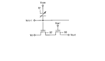
- Patent Document 1 describes a liquid crystal display device including a capacitance change detection circuit shown in FIG.
- the capacitance value of the variable capacitor 91 changes, and the gate voltage of a TFT (Thin Film Transistor) 92 changes accordingly. Therefore, when a high level selection voltage Vsel is applied to the gate electrode of the TFT 93, the read current output from the source electrode of the TFT 93 changes according to the capacitance value of the variable capacitor 91. Therefore, by comparing the output voltage Vout output from the source electrode of the TFT 93 with a threshold value, it can be determined whether or not the liquid crystal panel is pressed in the vicinity of the variable capacitor 91.
- Vsel Thin Film Transistor
- Patent Document 1 also describes a capacitance change detection circuit shown in FIG. In the circuit shown in FIG. 11, a control wiring connected to the gate electrode of the TFT 92 is added in order to apply the control voltage Vctrl to the gate electrode of the TFT 92.
- Patent Document 2 describes a method of detecting an increase in leakage current flowing through a transistor when a conductive protrusion is provided on a counter electrode of a display panel and the counter substrate is pressed with a pen.
- Patent Document 3 a variable capacitor is configured by a pair of electrodes on a substrate and a dielectric inserted between the electrodes, and the capacitance of the variable capacitor is changed by a physical or electrical force. A method of detecting is described.
- the gate electrode of the TFT 92 is an isolated electrode that is electrically separated from other portions.
- charges may be accumulated on the gate electrode of the TFT 92 due to the influence of static electricity or the like.
- the electrodes of the variable capacitor 91 are not completely insulated, when the electrodes of the variable capacitor 91 approach each other or come into contact with each other, the charge moves between the electrodes of the variable capacitor 91, and the moved charge is transferred to the TFT 92. May be accumulated on the gate electrode.
- the capacitance change detection circuit can control the gate voltage of the TFT connected to one electrode of the variable capacitor.
- the capacitance change detection circuit must have a function of releasing the charge accumulated in the gate electrode of the TFT connected to one electrode of the variable capacitor.
- the control wiring is connected to the capacitance change detection circuit for one row in the liquid crystal panel. Since many gate electrodes are connected to one control wiring, the load capacity of the control wiring is increased. For this reason, even if the capacitance of the variable capacitor 91 changes, the gate voltage of the TFT 92 changes only slightly. As a result, in the circuit shown in FIG. 11, it is difficult to detect a change in capacitance, and sensitivity is lowered.
- an object of the present invention is to provide a capacitance change detection circuit capable of detecting a capacitance change with high sensitivity and without malfunction.
- a first aspect of the present invention is a capacitance change detection circuit that detects a change in capacitance, A variable capacitor with one electrode connected to the voltage supply line; A detection transistor that has a gate electrode connected to the other electrode of the variable capacitor and outputs an electric signal corresponding to a capacitance value of the variable capacitor; A voltage application switching element provided between a control voltage line and a gate electrode of the detection transistor;
- the gate electrode of the detection transistor is It is characterized by maintaining a floating state.
- the first aspect of the present invention it further includes an output control switching element that is provided on a current path passing through the detection transistor and switches whether to output the electrical signal.
- a fourth aspect of the present invention is an image display device capable of detecting a touch position in a display screen, A display panel including a plurality of pixel circuits and one or more capacitance change detection circuits; A control circuit for the display panel,
- the capacitance change detection circuit includes: A variable capacitor with one electrode connected to the voltage supply line; A detection transistor that has a gate electrode connected to the other electrode of the variable capacitor and outputs an electric signal corresponding to a capacitance value of the variable capacitor; A voltage application switching element provided between a control voltage line and a gate electrode of the detection transistor.
- the display panel includes a plurality of capacitance change detection circuits arranged in a row direction and a column direction, The gate electrodes of the voltage application switching elements included in the capacitance change detection circuits arranged in the same row are connected to a common signal line.
- the gate voltage of the detection transistor is suitably controlled, and the detection transistor The charge accumulated in the gate electrode can be released, and malfunction of the circuit can be prevented. Also, the load capacity of the control voltage line is reduced by electrically separating the control voltage line and the gate electrode of the detection transistor using the voltage application transistor. For this reason, when the capacitance value of the variable capacitor changes, the gate voltage of the detection transistor changes greatly. Therefore, the capacitance change can be detected with high sensitivity.
- the state of the voltage application switching element is controlled, and a predetermined control voltage is applied to the control voltage line, whereby the gate voltage of the detection transistor is suitably controlled, and the capacitance Changes can be detected.
- the capacitance change detection circuit it is possible to switch whether or not to output an electrical signal from the capacitance change detection circuit by providing the output control switching element on the path of the current passing through the detection transistor. .
- the capacitance change detection circuit can be prevented from outputting an unnecessary electric signal.
- an image display device that can detect a touch position in a display screen with high sensitivity and without malfunction using a capacitance change detection circuit that can detect capacitance change with high sensitivity and without malfunction. Can do.
- the gate electrodes of the voltage application switching elements included in the capacitance change detection circuits arranged in the same row are used as a common signal. By connecting to the line, the number of signal lines used for controlling the capacitance change detection circuit can be reduced.
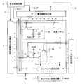
- FIG. 1 is a block diagram illustrating a configuration of a liquid crystal display device including a capacitance change detection circuit according to a first embodiment of the present invention.
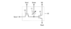
- 1 is a circuit diagram of a capacitance change detection circuit according to a first embodiment of the present invention.
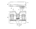
- FIG. 3 is a cross-sectional view showing a partial structure of the capacitance change detection circuit shown in FIG. 2.
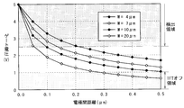
- FIG. 3 is a characteristic diagram of the capacitance change detection circuit shown in FIG. 2.
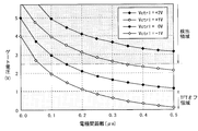
- FIG. 3 is a characteristic diagram of the capacitance change detection circuit shown in FIG. 2. It is a block diagram which shows the structure of the liquid crystal display device containing the capacity
- FIG. 6 is a circuit diagram of a capacitance change detection circuit according to a second embodiment of the present invention. It is a circuit diagram of the capacity
- FIG. 7 is a circuit diagram of a capacitance change detection circuit and a pixel circuit shown in FIG. 6.
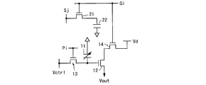
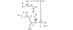
- FIG. 9B is a circuit diagram of a circuit (first example) in which signal lines are reduced from the circuit shown in FIG. 9A. It is a circuit diagram of the 2nd example similarly. Similarly, it is a circuit diagram of a third example. Similarly, it is a circuit diagram of a fourth example. Similarly, it is a circuit diagram of a fifth example.
- FIG. 1 is a block diagram showing a configuration of a liquid crystal display device including a capacitance change detection circuit according to the first embodiment of the present invention.
- the liquid crystal display device shown in FIG. 1 includes a liquid crystal panel 1, a display control circuit 2, a scanning signal line drive circuit 3, a data signal line drive circuit 4, a sensor control circuit 5, and a sensor output processing circuit 6.
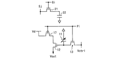
- the capacitance change detection circuit 10 according to the present embodiment is formed on the liquid crystal panel 1 together with the pixel circuit 20, and detects a change in capacitance when the surface of the liquid crystal panel 1 is pressed.
- the liquid crystal panel 1 has a structure in which a liquid crystal substance is sandwiched between two glass substrates.
- the liquid crystal panel 1 is provided with a plurality of scanning signal lines Gi parallel to each other and a plurality of parallel data signal lines Sj orthogonal to the scanning signal lines Gi.
- a pixel circuit 20 is provided in the vicinity of each intersection of the scanning signal line Gi and the data signal line Sj.
- the scanning signal lines Gi are connected to the pixel circuits 20 arranged in the same row, and the data signal lines Sj are connected to the pixel circuits 20 arranged in the same column.
- a capacitance change detection circuit 10 is provided for each pixel circuit 20.
- the same number of row selection lines Pi as the scanning signal lines Gi are provided in parallel with the scanning signal lines Gi.
- the row selection line Pi is connected to the capacitance change detection circuit 10 arranged in the same row.
- the liquid crystal panel 1 is also provided with a sensor output selection circuit 7 that selects the output of the capacitance change detection circuit 10.
- the pixel circuit 20 includes a TFT 21, a liquid crystal capacitor 22, and an auxiliary capacitor 23.
- the TFT 21 is an N channel type MOS transistor.
- the TFT 21 has a gate electrode connected to one scanning signal line Gi, a source electrode connected to one data signal line Sj, and a drain electrode connected to one electrode of the liquid crystal capacitor 22 and the auxiliary capacitor 23.
- the other electrode (counter electrode) of the liquid crystal capacitor 22 and the auxiliary capacitor 23 is connected to a voltage supply line (not shown) to which a common voltage Vcom is applied.
- the display control circuit 2, the scanning signal line driving circuit 3, the data signal line driving circuit 4, and the sensor control circuit 5 are control circuits for the liquid crystal panel 1.
- the display control circuit 2 outputs a control signal C1 to the scanning signal line driving circuit 3 and outputs a control signal C2 and a video signal DT to the data signal line driving circuit 4. Further, the display control circuit 2 outputs a control signal C3 to the sensor control circuit 5, and supplies a control voltage Vctrl to the liquid crystal panel 1.
- the scanning signal line driving circuit 3 selects one scanning signal line from the plurality of scanning signal lines Gi according to the control signal C1, and applies a gate-on voltage (voltage at which the TFT is turned on) to the selected scanning signal line. To do.
- the data signal line driving circuit 4 applies a voltage corresponding to the video signal DT to the data signal line Sj in accordance with the control signal C2. As a result, the pixel circuits 20 for one row can be selected, a voltage corresponding to the video signal DT can be written to the selected pixel circuits, and a desired image can be displayed.
- the sensor control circuit 5 selects one row selection line from the plurality of row selection lines Pi according to the control signal C3, and applies a gate-on voltage to the selected row selection line.
- the sensor control circuit 5 controls the sensor output selection circuit 7 according to the control signal C3.
- the sensor output selection circuit 7 selects one or more signals from the output signals of the plurality of capacitance change detection circuits 10 according to the control from the sensor control circuit 5, and outputs the selected signals to the outside of the liquid crystal panel 1.
- the sensor output processing circuit 6 obtains position data DP indicating the touch position in the display screen based on the signal output from the liquid crystal panel 1.
- FIG. 2 is a circuit diagram of the capacitance change detection circuit 10.
- the capacitance change detection circuit 10 includes a variable capacitor 11 and TFTs 12 and 13.
- the TFTs 12 and 13 are N channel type MOS transistors.
- One electrode of the variable capacitor 11 is connected to a voltage supply line to which a common voltage Vcom is applied, and the other electrode is connected to the gate electrode of the TFT 12.
- a drain voltage Vd supplied from the outside of the liquid crystal panel 1 is applied to the drain electrode of the TFT 12, and an output voltage Vout is output from the source electrode.
- the gate electrode of the TFT 13 is connected to the row selection line Pi to which the selection voltage Vsel is applied.
- One of the other two electrodes of the TFT 13 is connected to the control voltage line to which the control voltage Vctrl is applied, and the other is connected to the gate electrode of the TFT 12.
- the TFT 12 functions as a detection transistor that outputs an electrical signal corresponding to the capacitance value of the variable capacitor 11.
- the TFT 13 functions as a voltage application switching element provided between the control voltage line and the gate electrode of the TFT 12.
- FIG. 3 is a cross-sectional view showing a part of the structure of the capacitance change detection circuit 10.
- FIG. 3 shows a counter substrate 30 in which a counter electrode 33 is formed on a glass substrate 31 and a TFT side substrate 40 in which a TFT 12 and the like are formed on a glass substrate 41.
- a protrusion 32 is provided on one surface of the counter substrate 30 (the surface facing the TFT side substrate 40; the lower surface in FIG. 3), and ITO (Indium / Tin / Oxide) is formed thereon.
- ITO Indium / Tin / Oxide
- the counter electrode 33 is formed.
- Various circuits are formed on one surface of the TFT side substrate 40 (the surface facing the counter substrate 30; the upper surface in FIG.
- the counter substrate 30 and the TFT side substrate 40 are arranged to face each other, and a liquid crystal substance (not shown) is filled between the both substrates. Thereby, the liquid crystal capacitor 22 and the variable capacitor 11 are formed.
- the distance between the counter electrode 33 and the variable capacitance electrode 42 is shorter in the portion where the protrusion 32 is provided than in other portions.
- a variable capacitor 11 is formed in this portion.
- the counter electrode 33 formed in the portion where the protrusion 32 is provided becomes one electrode of the variable capacitor 11 (the electrode to which the common voltage Vcom is applied), and the variable capacitor formed in the portion facing the portion where the protrusion 32 is provided.
- the electrode 42 becomes the other electrode of the variable capacitor 11.
- the variable capacitance electrode 42 is separated from the pixel electrode.
- the TFT 12 having the gate electrode 43, the source electrode 44 and the drain electrode 45 is formed in the vicinity of the variable capacitor 11.
- the gate electrode 43 is electrically connected to the other electrode of the variable capacitor 11 through the contact 46.
- a common voltage Vcom is applied to the counter electrode 33.
- the interelectrode distance (distance d shown in FIG. 3) of the variable capacitor 11 is reduced.
- the inter-electrode distance d changes, the capacitance value of the variable capacitor 11 changes, and accordingly, the gate voltage of the TFT 12 changes and the output voltage Vout also changes. Therefore, it is possible to determine whether or not the liquid crystal panel 1 has been pressed in the vicinity of the variable capacitor 11 by comparing the output voltage Vout with a threshold value.
- FIG. 4 is a characteristic diagram of the capacitance change detection circuit 10.
- FIG. 4 shows the relationship between the interelectrode distance d of the variable capacitor 11 and the gate voltage Vg of the TFT 12 when the common voltage Vcom is DC 5 V and the channel width W of the TFT 12 is changed.
- the gate voltage Vg increases as the interelectrode distance d decreases, and becomes equal to the common voltage 5 V when the interelectrode distance d is zero.
- the gate voltage Vg increases as the channel width W decreases.
- the N-channel TFT 12 is turned on when the gate voltage Vg is equal to or higher than the threshold voltage.
- the gate voltage Vg is close to the threshold voltage, since the read current flowing through the TFT 12 is small, it takes time to change the output voltage Vout. Therefore, a boundary voltage Vb higher than the threshold voltage is set, and if the gate voltage Vg is equal to or higher than the boundary voltage Vb, it is determined that there is a capacity change (that is, the liquid crystal panel 1 is pressed).
- the threshold voltage of the TFT 12 is 1V
- the boundary voltage Vb is 2.5V.
- the channel width W is 4 ⁇ m, it is determined that there is a capacitance change when the inter-electrode distance d is about 0.2 ⁇ m or less.
- the channel width W is 20 ⁇ m, it is determined that the capacitance has changed when the inter-electrode distance d is about 0.05 ⁇ m or less.
- the sensitivity of the capacitance change detection circuit 10 changes according to the channel width W of the TFT 12.
- the channel width W of the TFT 12 is arbitrarily determined according to the application.
- FIG. 5 is a diagram showing the same relationship as FIG. 4 in the case where the gate voltage is applied to the gate electrode of the TFT 13 to change the control voltage Vctrl.
- the characteristics shown in FIG. 5 are obtained for the capacitance change detection circuit 10 shown below.
- the size of the electrode of the variable capacitor 11 is 4 ⁇ 4 ⁇ m.
- the interelectrode distance d of the variable capacitor 11 varies between 0 ⁇ m and 0.5 ⁇ m.
- the dielectric constant of the liquid crystal is 4 for the amount ⁇ (//) in the direction parallel to the major axis of the liquid crystal and 7 for the amount ⁇ ( ⁇ ) in the direction perpendicular to the major axis of the liquid crystal.
- the channel width and channel length of the TFTs 12 and 13 are both 4 ⁇ m, and the thickness of the gate insulating film is 80 nm.
- the common voltage Vcom is 5 V DC
- the control voltage Vctrl is 0 V
- the threshold voltage Vth of the TFT 12 is 1 V
- the initial value of the output voltage Vout is 0 V
- the initial value of the interelectrode distance d of the variable capacitor 11 is 0.5 ⁇ m.
- the capacitance change detection circuit 10 has the characteristics shown in FIG. 5, and a voltage at which the TFT is turned off is called a gate-off voltage.
- a gate-on voltage (for example, 5 V) is applied to the gate electrode of the TFT 13.
- the TFT 13 is turned on, and the control voltage 0 V applied to the control voltage line is applied to the gate electrode of the TFT 12 via the TFT 13. Since the control voltage 0V is lower than the threshold voltage 1V of the TFT 12, the TFT 12 is turned off regardless of the capacitance value of the variable capacitor 11. Since the output voltage Vout does not change at this time, the output voltage Vout remains 0 V even after the TFT 12 is turned off.
- a gate-off voltage (for example, 0 V) is applied to the gate electrode of the TFT 13.
- the TFT 13 is turned off, and the gate electrode of the TFT 12 is in a floating state.
- the gate voltage Vg of the TFT 12 is about 1 V (see FIG. 5).
- the output voltage Vout remains at about 0V.
- the inter-electrode distance d of the variable capacitor 11 decreases.
- the capacitance value of the variable capacitor 11 increases, and the gate voltage Vg of the TFT 12 increases.
- the TFT 13 is controlled to be turned on, so that the control voltage Vctrl is applied to the gate electrode of the TFT 12, and the TFT 13 is controlled to be turned off, so that the gate electrode of the TFT 12 is brought into a floating state. Can be set.
- the TFT 13 is controlled to be in the ON state, the charges accumulated in the gate electrode of the TFT 12 are released, and the gate voltage of the TFT 12 is set to the control voltage.
- the capacitance change detection circuit 10 according to the present embodiment, the capacitance change when the surface of the liquid crystal panel 1 is pressed can be detected with high sensitivity.
- the capacitance change detection circuit 10 by applying the control voltage Vctrl to the gate electrode of the TFT 12 via the TFT 13, the capacitance change can be detected with high sensitivity and without malfunction. it can. Further, by using the capacitance change detection circuit 10, it is possible to configure an image display device that can detect the touch position in the display screen with high sensitivity and without malfunction. Further, when the capacitance change detection circuit 10 is two-dimensionally arranged, the capacitance change is obtained by connecting the gate electrode of the TFT 13 included in the capacitance change detection circuit 10 arranged in the same row to the common row selection line Pi. The number of signal lines used for control of the detection circuit 10 can be reduced.
- FIG. 6 is a block diagram showing a configuration of a liquid crystal display device including a capacitance change detection circuit according to the second embodiment of the present invention.
- the liquid crystal display device shown in FIG. 6 is obtained by replacing the liquid crystal panel 1 and the sensor control circuit 5 with the liquid crystal panel 8 and the sensor control circuit 9 in the liquid crystal display device (FIG. 1) according to the first embodiment.
- the capacitance change detection circuit 15 according to the present embodiment is formed on the liquid crystal panel 8 together with the pixel circuit 20, and detects a change in capacitance when the surface of the liquid crystal panel 8 is pressed.
- the same referential mark is attached
- the liquid crystal panel 8 includes a plurality of scanning signal lines Gi, a plurality of data signal lines Sj, a plurality of row selection lines Pi (hereinafter referred to as first row selection lines Pi), and a plurality of pixel circuits 20.
- a plurality of capacitance change detection circuits 15 and a sensor output selection circuit 7 are provided.
- the liquid crystal panel 8 is provided with the same number of second row selection lines Qi as the first row selection lines Pi in parallel with the first row selection lines Pi. Similar to the first row selection line Pi, the second row selection line Qi is connected to the capacitance change detection circuit 15 arranged in the same row.
- the sensor control circuit 9 selects the first row selection line Pi according to the control signal C3, and controls the sensor output selection circuit 7. In addition to this, the sensor control circuit 9 selects one second row selection line from the plurality of second row selection lines Qi in accordance with the control signal C3, and applies a gate-on voltage to the selected second row selection line. . The sensor control circuit 9 selects the first row selection line Pi and the second row selection line Qi at different timings.
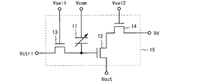
- FIG. 7 is a circuit diagram of the capacitance change detection circuit 15.
- the capacitance change detection circuit 15 shown in FIG. 7 is obtained by adding a TFT 14 to the capacitance change detection circuit 10 (FIG. 2) according to the first embodiment.
- the TFT 14 is an N channel type MOS transistor.
- the gate electrode of the TFT 13 is connected to the first row selection line Pi to which the first row selection voltage Vsel1 is applied.
- the drain electrode of the TFT 12 is connected to the source electrode of the TFT 14.
- the gate electrode of the TFT 14 is connected to the second row selection line Qi to which the second row selection voltage Vsel2 is applied, and the drain voltage Vd supplied from the outside of the liquid crystal panel 8 is applied to the drain electrode.
- the TFT 14 is provided on a current path passing through the TFT 12 and functions as an output control switching element that switches whether to output the output voltage Vout.
- the TFT 14 is controlled by the sensor control circuit 9 to be on or off.
- the capacitance change detection circuit 15 outputs the output voltage Vout when the TFT 14 is on, and does not output the output voltage Vout when the TFT 14 is off. As described above, according to the capacitance change detection circuit 15 according to the present embodiment, whether the output voltage Vout is output or not can be switched by providing the TFT 14 on the path of the current passing through the TFT 12.
- the gate voltage of the TFT 12 when the capacitance value of the variable capacitor 11 subsequently changes according to the capacitance value of the variable capacitor 11 when the control voltage Vctrl is applied to the gate electrode of the TFT 12. Changes. Accordingly, the first row selection line Pi and the second row selection line Qi are selected at different timings, and the application of the control voltage Vctrl and the selection of the capacitance change detection circuit 15 are performed at different timings. The relationship with the capacitance value of 11 can always be kept constant.
- the TFT 14 is provided on the drain electrode side of the TFT 12, but the TFT 14 may be provided on the source electrode side of the TFT 12 as shown in FIG.
- the drain voltage Vd is applied to the drain electrode of the TFT 12, and the source electrode is connected to the drain electrode of the TFT 14.
- An output voltage Vout is output from the source electrode of the TFT 14.
- the capacitance change detection circuit 16 according to this modification operates in the same manner as the capacitance change detection circuit 15 and has the same effect.
- the liquid crystal panel is provided with the capacitance change detection circuit for each pixel circuit.
- the liquid crystal panel may be provided with any number of capacitance change detection circuits in an arbitrary form.
- the capacitance change detection circuit may be provided corresponding to two or more pixel circuits, or the capacitance change detection circuit may be provided only in a part of the liquid crystal panel without corresponding to the pixel circuit.
- any type of wiring is provided in the liquid crystal panel in any form. Also good.
- the common voltage Vcom may be a DC voltage or an AC voltage.
- FIG. 9A is a circuit diagram of the capacitance change detection circuit 15 and the pixel circuit 20 shown in FIG. 6 (excluding the auxiliary capacitor 23). With respect to this circuit, the number of signal lines provided in the liquid crystal panel can be reduced by the seven methods exemplified below.
- the gate electrode of the output control switching element (TFT14) and the gate electrode of the writing switching element (TFT21) in the pixel circuit are connected to the same signal line (scanning signal line Gi). Good.
- the gate electrode and the drain electrode of the output control switching element (TFT 14) may be connected to the same signal line (second row selection line Qi).
- the gate electrode of the voltage application switching element (TFT13) and the gate electrode of the writing switching element (TFT21) may be connected to the same signal line (scanning signal line Gi).
- FIG. 9B the gate electrode of the output control switching element (TFT14) and the gate electrode of the writing switching element (TFT21) in the pixel circuit are connected to the same signal line (scanning signal line Gi).
- the gate electrode and the drain electrode of the output control switching element (TFT 14) may be connected to the same signal line (second row selection line Qi).
- the gate electrode of the voltage application switching element (TFT13) and the gate electrode of the writing switching element (TFT21) may be
- the gate electrode of the voltage application switching element (TFT13) and the gate electrode of the output control switching element (TFT17) may be connected to the same signal line (first row selection line Pi). .
- a P-channel TFT 17 is used.
- the source electrode of the detection transistor (TFT12) and the source electrode of the write switching element (TFT21) may be connected to the same signal line (data signal line Sj).
- one electrode of the voltage applying switching element (TFT13) and the source electrode of the writing switching element (TFT21) may be connected to the same signal line (data signal line Sj).
- one electrode of the voltage application switching element (TFT 13) and the common electrode of the liquid crystal capacitor 22 may be connected to the same signal line (control voltage line to which the control voltage Vctrl is applied).
- the number of signal lines provided in the liquid crystal panel can be further reduced by suitably combining the above seven methods.
- the capacitance change detection circuit of the present invention has a feature that it can detect a capacitance change with high sensitivity and without malfunction, the capacitance change detection circuit of the present invention is used for various applications for detecting a capacitance change, such as an application for detecting a touch position in a display screen in an image display device. Can be used.
Landscapes
- Engineering & Computer Science (AREA)
- General Engineering & Computer Science (AREA)
- Theoretical Computer Science (AREA)
- Human Computer Interaction (AREA)
- Physics & Mathematics (AREA)
- General Physics & Mathematics (AREA)
- Liquid Crystal (AREA)
- Control Of Indicators Other Than Cathode Ray Tubes (AREA)
- Position Input By Displaying (AREA)
Abstract
液晶パネル1の表面を押すと、可変容量11の容量値が変化する。可変容量11の一方の電極は共通電圧Vcomを印加した電圧供給線に接続され、他方の電極はTFT12のゲート電極に接続される。TFT12は、可変容量11の容量値に応じた電圧Voutを出力する。TFT13は制御電圧Vctrlを印加した制御電圧線とTFT12のゲート電極の間に設けられ、TFT13のゲート電極は行選択線Piに接続される。TFT13を設けることにより、TFT12のゲート電極に所望の電圧を印加し、当該電極に蓄積された電荷を逃がして、回路の誤動作を防止することができる。制御電圧線の負荷容量を減らすことにより、容量変化を高い感度で検出することができる。これにより、容量変化を高い感度で誤動作なく検出できる容量変化検出回路を提供する。
Description
本発明は、静電容量の変化を検出する容量変化検出回路に関する。本発明の容量変化検出回路は、例えば画像表示装置の表示パネル上に形成され、表示画面内のタッチ位置を検出する用途などに利用される。
近年、指やペンなどで画面に触れることにより操作可能な電子機器が普及している。また、表示画面内のタッチ位置を検出する方法として、表示パネルに複数の容量変化検出回路を設け、指やペンなどで表示パネルの表面を押したときの静電容量の変化を検出する方法が知られている。
特許文献1には、図10に示す容量変化検出回路を備えた液晶表示装置が記載されている。図10に示す回路では、液晶パネルの表面を押したときに、可変容量91の容量値が変化し、これに伴いTFT(Thin Film Transistor:薄膜トランジスタ)92のゲート電圧が変化する。このため、TFT93のゲート電極にハイレベルの選択電圧Vselを与えたときに、TFT93のソース電極から出力される読み出し電流は可変容量91の容量値に応じて変化する。したがって、TFT93のソース電極から出力される出力電圧Voutを閾値と比較することにより、可変容量91の近傍で液晶パネルが押されたか否かを判定することができる。特許文献1には、図11に示す容量変化検出回路も記載されている。図11に示す回路には、TFT92のゲート電極に制御電圧Vctrlを印加するために、TFT92のゲート電極に接続する制御配線が追加されている。
これ以外に本願発明に関連する技術は、特許文献2、3に記載されている。特許文献2には、表示パネルの対向電極に導電性の突起を設け、対向基板がペンで押されたときにトランジスタを流れるリーク電流の増加を検出する方法が記載されている。特許文献3には、基板上の1対の電極と電極間に挿入された誘電体で可変容量を構成し、物理的あるいは電気的な力で可変容量の電気容量を変化させることにより、外部入力を検出する方法が記載されている。
図10に示す回路では、TFT92のゲート電極は、他の部分から電気的に切り離された孤立電極となる。しかしながら、TFT作製工程において、静電気などの影響によりTFT92のゲート電極に電荷が蓄積されることがある。また、可変容量91の電極間が完全に絶縁されていない場合には、可変容量91の電極が互いに接近あるいは接触したときに、可変容量91の電極間を電荷が移動し、移動した電荷がTFT92のゲート電極に蓄積されることがある。
TFT92のゲート電極に電荷が蓄積されると、TFT92の閾値電圧が変化し、出力電圧Voutも変化する。このため、図10に示す回路は、誤動作することがある。この誤動作を防止するために、容量変化検出回路は、可変容量の一方の電極に接続されたTFTのゲート電圧を制御できることが好ましい。また、可変容量91の電極が互いに接近あるいは接触したときにTFT92のゲート電極に一定以上の電荷が蓄積されると、可変容量91の電極間距離が元に戻った後もTFT92が引き続きオン状態になることが問題となる。この問題を解決するためには、容量変化検出回路には、可変容量の一方の電極に接続されたTFTのゲート電極に蓄積された電荷を逃がす機能が必須となる。
図11に示す回路では、TFT92のゲート電極は孤立電極ではないので、上記の問題は生じない。しかしながら、この回路では、制御配線は液晶パネル内の1行分の容量変化検出回路に接続されている。1本の制御配線に多数のゲート電極が接続されるので、制御配線の負荷容量は大きくなる。このため、可変容量91の容量が変化しても、TFT92のゲート電圧はわずかしか変化しない。この結果、図11に示す回路では容量変化の検出が困難になり、感度が低下する。
それ故に、本発明は、容量変化を高い感度で誤動作なく検出できる容量変化検出回路を提供することを目的とする。
本発明の第1の局面は、静電容量の変化を検出する容量変化検出回路であって、
一方の電極が電圧供給線に接続された可変容量と、
ゲート電極が前記可変容量の他方の電極に接続され、前記可変容量の容量値に応じた電気信号を出力する検出用トランジスタと、
制御電圧線と前記検出用トランジスタのゲート電極との間に設けられた電圧印加用スイッチング素子とを備える。
一方の電極が電圧供給線に接続された可変容量と、
ゲート電極が前記可変容量の他方の電極に接続され、前記可変容量の容量値に応じた電気信号を出力する検出用トランジスタと、
制御電圧線と前記検出用トランジスタのゲート電極との間に設けられた電圧印加用スイッチング素子とを備える。
本発明の第2の局面は、本発明の第1の局面において、
前記電圧印加用スイッチング素子がオン状態である間に、所定の制御電圧が前記制御電圧線に印加され、前記電圧印加用スイッチング素子がオフ状態に変化した後は、前記検出用トランジスタのゲート電極はフローティング状態を保つことを特徴とする。
前記電圧印加用スイッチング素子がオン状態である間に、所定の制御電圧が前記制御電圧線に印加され、前記電圧印加用スイッチング素子がオフ状態に変化した後は、前記検出用トランジスタのゲート電極はフローティング状態を保つことを特徴とする。
本発明の第3の局面は、本発明の第1の局面において、
前記検出用トランジスタを通過する電流の経路上に設けられ、前記電気信号を出力するか否かを切り替える出力制御用スイッチング素子をさらに備える。
前記検出用トランジスタを通過する電流の経路上に設けられ、前記電気信号を出力するか否かを切り替える出力制御用スイッチング素子をさらに備える。
本発明の第4の局面は、表示画面内のタッチ位置を検出できる画像表示装置であって、
複数の画素回路と1以上の容量変化検出回路とを含む表示パネルと、
前記表示パネルの制御回路とを備え、
前記容量変化検出回路は、
一方の電極が電圧供給線に接続された可変容量と、
ゲート電極が前記可変容量の他方の電極に接続され、前記可変容量の容量値に応じた電気信号を出力する検出用トランジスタと、
制御電圧線と前記検出用トランジスタのゲート電極との間に設けられた電圧印加用スイッチング素子とを含む。
複数の画素回路と1以上の容量変化検出回路とを含む表示パネルと、
前記表示パネルの制御回路とを備え、
前記容量変化検出回路は、
一方の電極が電圧供給線に接続された可変容量と、
ゲート電極が前記可変容量の他方の電極に接続され、前記可変容量の容量値に応じた電気信号を出力する検出用トランジスタと、
制御電圧線と前記検出用トランジスタのゲート電極との間に設けられた電圧印加用スイッチング素子とを含む。
本発明の第5の局面は、本発明の第4の局面において、
前記表示パネルは、行方向および列方向に配置された複数の容量変化検出回路を含み、
同じ行に配置された容量変化検出回路に含まれる電圧印加用スイッチング素子のゲート電極は、共通の信号線に接続されていることを特徴とする。
前記表示パネルは、行方向および列方向に配置された複数の容量変化検出回路を含み、
同じ行に配置された容量変化検出回路に含まれる電圧印加用スイッチング素子のゲート電極は、共通の信号線に接続されていることを特徴とする。
本発明の第1の局面によれば、制御電圧線と検出用トランジスタのゲート電極との間に電圧印加用スイッチング素子を設けることにより、検出用トランジスタのゲート電圧を好適に制御し、検出用トランジスタのゲート電極に蓄積された電荷を逃がして、回路の誤動作を防止することができる。また、電圧印加用トランジスタを用いて制御電圧線と検出用トランジスタのゲート電極とを電気的に切り離すことにより、制御電圧線の負荷容量は小さくなる。このため、可変容量の容量値が変化したときに、検出用トランジスタのゲート電圧は大きく変化する。したがって、容量変化を高い感度で検出することができる。
本発明の第2の局面によれば、電圧印加用スイッチング素子の状態を制御すると共に、制御電圧線に所定の制御電圧を印加することにより、検出用トランジスタのゲート電圧を好適に制御し、容量変化を検出することができる。
本発明の第3の局面によれば、検出用トランジスタを通過する電流の経路上に出力制御用スイッチング素子を設けることにより、容量変化検出回路から電気信号を出力するか否かを切り替えることができる。これにより、検出用トランジスタが完全にオフ状態にならないときでも、容量変化検出回路が不要な電気信号を出力しないようにすることができる。
本発明の第4の局面によれば、容量変化を高い感度で誤動作なく検出できる容量変化検出回路を用いて、表示画面内のタッチ位置を高い感度で誤動作なく検出できる画像表示装置を構成することができる。
本発明の第5の局面によれば、容量変化検出回路を2次元状に配置したときに、同じ行に配置された容量変化検出回路に含まれる電圧印加用スイッチング素子のゲート電極を共通の信号線に接続することにより、容量変化検出回路の制御に使用する信号線を減らすことができる。
(第1の実施形態)
図1は、本発明の第1の実施形態に係る容量変化検出回路を含む液晶表示装置の構成を示すブロック図である。図1に示す液晶表示装置は、液晶パネル1、表示制御回路2、走査信号線駆動回路3、データ信号線駆動回路4、センサ制御回路5、および、センサ出力処理回路6を備えている。本実施形態に係る容量変化検出回路10は、画素回路20と共に液晶パネル1上に形成され、液晶パネル1の表面が押されたときの静電容量の変化を検出する。
図1は、本発明の第1の実施形態に係る容量変化検出回路を含む液晶表示装置の構成を示すブロック図である。図1に示す液晶表示装置は、液晶パネル1、表示制御回路2、走査信号線駆動回路3、データ信号線駆動回路4、センサ制御回路5、および、センサ出力処理回路6を備えている。本実施形態に係る容量変化検出回路10は、画素回路20と共に液晶パネル1上に形成され、液晶パネル1の表面が押されたときの静電容量の変化を検出する。
液晶パネル1は、2枚のガラス基板の間に液晶物質を挟み込んだ構造を有する。液晶パネル1には、互いに平行な複数の走査信号線Giと、走査信号線Giと直交する互いに平行な複数のデータ信号線Sjとが設けられる。走査信号線Giとデータ信号線Sjの各交点の近傍には、画素回路20が設けられる。走査信号線Giは同じ行に配置された画素回路20に接続され、データ信号線Sjは同じ列に配置された画素回路20に接続される。画素回路20のそれぞれに対応して、容量変化検出回路10が設けられる。また、走査信号線Giと平行に走査信号線Giと同数の行選択線Piが設けられる。行選択線Piは、同じ行に配置された容量変化検出回路10に接続される。液晶パネル1には、容量変化検出回路10の出力を選択するセンサ出力選択回路7も設けられる。
画素回路20は、TFT21、液晶容量22、および、補助容量23を含んでいる。TFT21は、Nチャネル型MOSトランジスタである。TFT21のゲート電極は1本の走査信号線Giに接続され、ソース電極は1本のデータ信号線Sjに接続され、ドレイン電極は液晶容量22と補助容量23の一方の電極に接続される。液晶容量22と補助容量23の他方の電極(対向電極)は、共通電圧Vcomを印加した電圧供給線(図示せず)に接続される。
表示制御回路2、走査信号線駆動回路3、データ信号線駆動回路4およびセンサ制御回路5は、液晶パネル1の制御回路である。表示制御回路2は、走査信号線駆動回路3に対して制御信号C1を出力し、データ信号線駆動回路4に対して制御信号C2と映像信号DTを出力する。また、表示制御回路2は、センサ制御回路5に対して制御信号C3を出力し、液晶パネル1に対して制御電圧Vctrlを供給する。
走査信号線駆動回路3は、制御信号C1に従い複数の走査信号線Giの中から1本の走査信号線を選択し、選択した走査信号線にゲートオン電圧(TFTがオン状態になる電圧)を印加する。データ信号線駆動回路4は、制御信号C2に従い、映像信号DTに応じた電圧をデータ信号線Sjに印加する。これにより1行分の画素回路20を選択し、選択した画素回路に対して映像信号DTに応じた電圧を書き込み、所望の画像を表示することができる。
センサ制御回路5は、制御信号C3に従い複数の行選択線Piの中から1本の行選択線を選択し、選択した行選択線にゲートオン電圧を印加する。また、センサ制御回路5は、制御信号C3に従いセンサ出力選択回路7を制御する。センサ出力選択回路7は、センサ制御回路5からの制御に従い、複数の容量変化検出回路10の出力信号の中から1以上の信号を選択し、選択した信号を液晶パネル1の外部に出力する。センサ出力処理回路6は、液晶パネル1から出力された信号に基づき、表示画面内のタッチ位置を示す位置データDPを求める。
図2は、容量変化検出回路10の回路図である。図2に示すように、容量変化検出回路10は、可変容量11、および、TFT12、13を含んでいる。TFT12、13は、Nチャネル型MOSトランジスタである。可変容量11の一方の電極は共通電圧Vcomを印加した電圧供給線に接続され、他方の電極はTFT12のゲート電極に接続される。TFT12のドレイン電極には液晶パネル1の外部から供給されたドレイン電圧Vdが印加され、ソース電極からは出力電圧Voutが出力される。TFT13のゲート電極は、選択電圧Vselを印加した行選択線Piに接続される。TFT13の他の2個の電極のうち一方は制御電圧Vctrlを印加した制御電圧線に接続され、他方はTFT12のゲート電極に接続される。TFT12は、可変容量11の容量値に応じた電気信号を出力する検出用トランジスタとして機能する。TFT13は、制御電圧線とTFT12のゲート電極との間に設けられた電圧印加用スイッチング素子として機能する。
図3は、容量変化検出回路10の一部の構造を示す断面図である。図3には、ガラス基板31上に対向電極33を形成した対向基板30と、ガラス基板41上にTFT12などを形成したTFT側基板40とが記載されている。対向基板30の一方の面(TFT側基板40に対向する面;図3では下側の面)には突起物32が設けられ、その上にITO(Indium Tin Oxide:酸化インジウムスズ)を成膜することにより対向電極33が形成される。TFT側基板40の一方の面(対向基板30に対向する面;図3では上側の面)には各種の回路が形成され、その上にITOを成膜することにより画素電極と可変容量電極42が形成される。対向基板30とTFT側基板40は対向して配置され、両基板の間には液晶物質(図示ぜず)が充填される。これにより、液晶容量22と可変容量11が形成される。
突起物32を設けた部分では他の部分と比べて、対向電極33と可変容量電極42の間の距離が短くなる。この部分に可変容量11が形成される。突起物32を設けた部分に形成された対向電極33が可変容量11の一方の電極(共通電圧Vcomを印加した電極)となり、突起物32を設けた部分に対向する部分に形成された可変容量電極42が可変容量11の他方の電極となる。可変容量電極42は、画素電極から分離されている。
TFT側基板40において可変容量11の近傍には、ゲート電極43、ソース電極44およびドレイン電極45を有するTFT12が形成される。ゲート電極43は、コンタクト46を介して可変容量11の他方の電極に電気的に接続される。対向電極33には共通電圧Vcomが印加される。この状態で対向基板30の表面を指やペンなどで押すと、対向基板30はTFT側基板40に接近し、可変容量11の電極間距離(図3に示す距離d)は小さくなる。電極間距離dが変化すると、可変容量11の容量値は変化し、これに伴いTFT12のゲート電圧は変化し、出力電圧Voutも変化する。したがって、出力電圧Voutを閾値と比較することにより、可変容量11の近傍で液晶パネル1が押されたか否かを判定することができる。
図4は、容量変化検出回路10の特性図である。図4には、共通電圧Vcomを直流5Vとし、TFT12のチャネル幅Wを変化させた場合について、可変容量11の電極間距離dとTFT12のゲート電圧Vgとの関係が記載されている。図4に示すように、ゲート電圧Vgは電極間距離dが小さいほど高くなり、電極間距離dが0のときには共通電圧5Vに等しくなる。また、ゲート電圧Vgはチャネル幅Wが狭いほど高くなる。
Nチャネル型のTFT12は、ゲート電圧Vgが閾値電圧以上のときにオン状態になる。しかし、ゲート電圧Vgが閾値電圧に近いときには、TFT12を流れる読み出し電流が少ないので、出力電圧Voutの変化に時間がかかる。そこで、閾値電圧よりも高い境界電圧Vbを設定し、ゲート電圧Vgが境界電圧Vb以上であれば、容量変化あり(すなわち、液晶パネル1が押された)と判断することにする。ここでは、TFT12の閾値電圧を1V、境界電圧Vbを2.5Vとする。図4には、ゲート電圧Vgが閾値電圧以下である範囲(TFTオフ領域)と、ゲート電圧Vgが境界電圧以上である範囲(検出領域)とが記載されている。なお、2.5Vは境界電圧Vbの一例であり、境界電圧Vbは用途などに応じて任意に決定される。
図4に示すように、チャネル幅Wが4μmのときには、電極間距離dが約0.2μm以下になると、容量変化ありと判断される。一方、チャネル幅Wが20μmのときには、電極間距離dが約0.05μm以下になると、容量変化ありと判断される。このように容量変化検出回路10の感度は、TFT12のチャネル幅Wに応じて変化する。TFT12のチャネル幅Wは、用途などに応じて任意に決定される。
図5は、図4と同様の関係を、TFT13のゲート電極にゲートオン電圧を印加して、制御電圧Vctrlを変化させた場合について示す図である。図5に示す特性は、以下に示す容量変化検出回路10について求めたものである。可変容量11の電極のサイズは4×4μmである。可変容量11の電極間距離dは0μm~0.5μmの間で変化する。液晶の誘電係数は、液晶長軸に平行な方向の分量ε(//)が4、液晶長軸に垂直な方向の分量ε(⊥)が7である。TFT12、13のチャネル幅とチャネル長はいずれも4μmであり、ゲート絶縁膜の厚さは80nmである。
図5に示すように、制御電圧Vctrlが+2Vのときは、電極間距離dが0.5μm以下である限り、常に容量変化ありと判断される。制御電圧Vctrlが+1Vのときには、電極間距離dが約0.35μm以下になると、容量変化ありと判断される。制御電圧Vctrlを0Vおよび-1Vに変化させたときに、容量変化ありと判断されるための条件は、電極間距離dが約0.15μm以下および約0.06μm以下に変化する。このように制御電圧Vctrlを変化させることにより、TFT12のゲート電圧を好適に制御し、容量変化検出回路10の感度を調整することができる。
以下、容量変化検出回路10の動作を説明する。以下の説明では、共通電圧Vcomは直流5V、制御電圧Vctrlは0V、TFT12の閾値電圧Vthは1V、出力電圧Voutの初期値は0V、可変容量11の電極間距離dの初期値は0.5μm、であるとする。また、容量変化検出回路10は図5に示す特性を有するものとし、TFTがオフ状態になる電圧をゲートオフ電圧という。
まず、TFT13のゲート電極には、ゲートオン電圧(例えば、5V)が印加される。このときTFT13はオン状態になり、制御電圧線に印加された制御電圧0VはTFT13を経由してTFT12のゲート電極に印加される。制御電圧0VはTFT12の閾値電圧1Vよりも低いので、可変容量11の容量値にかかわらず、TFT12はオフ状態になる。このときに出力電圧Voutは変化しないので、TFT12がオフ状態になった後も出力電圧Voutは0Vのままである。
次に、TFT13のゲート電極には、ゲートオフ電圧(例えば、0V)が印加される。このときTFT13はオフ状態になり、TFT12のゲート電極はフローティング状態になる。このときに可変容量11の電極間距離dが初期値0.5μmであれば、TFT12のゲート電圧Vgは約1Vとなる(図5を参照)。出力電圧Voutは約0Vのままである。
対向基板30の表面を指やペンなどで押すと、可変容量11の電極間距離dは小さくなる。このとき可変容量11の容量値は増大し、TFT12のゲート電圧Vgは上昇する。例えば、電極間距離dが0.1μmになると、TFT12のゲート電圧Vgは約3Vとなる。また、Vout=Vg-Vthより、出力電圧Voutは約2Vとなる。TFT12の閾値電圧Vthを考慮して出力電圧Voutを境界電圧Vbと比較することにより、容量変化ありと判断される。
このように容量変化検出回路10では、TFT13をオン状態に制御することにより、TFT12のゲート電極に制御電圧Vctrlを印加し、TFT13をオフ状態に制御することにより、TFT12のゲート電極をフローティング状態に設定することができる。これにより、フローティング状態のTFT12のゲート電極に電荷が蓄積されていた場合でも、TFT13をオン状態に制御したときに、TFT12のゲート電極に蓄積されていた電荷を逃がし、TFT12のゲート電圧を制御電圧Vctrlに等しくすることができる。このため、TFT作製工程で電荷がTFT12のゲート端子に蓄積される場合や、使用時に対向電極33から移動した電荷がTFT12のゲート端子に蓄積される場合でも、TFT12のゲート電圧がこれらの電荷の影響を受けることがない。したがって、容量変化検出回路10によれば、回路の誤動作を防止することができる。
また、TFT13を用いて制御電圧線とTFT12のゲート電極を電気的に切り離すことにより、制御電圧線の負荷容量は図11に示す従来の回路よりも小さくなる。このため、可変容量11の容量値が変化したときに、TFT12のゲート電圧は大きく変化する。したがって、本実施形態に係る容量変化検出回路10によれば、液晶パネル1の表面が押されたときの容量変化を高い感度で検出することができる。
以上に示すように、本実施形態に係る容量変化検出回路10によれば、TFT13を介してTFT12のゲート電極に制御電圧Vctrlを印加することにより、容量変化を高い感度で誤動作なく検出することができる。また、容量変化検出回路10を用いることにより、表示画面内のタッチ位置を高い感度で誤動作なく検出できる画像表示装置を構成することができる。また、容量変化検出回路10を2次元状に配置したときに、同じ行に配置された容量変化検出回路10に含まれるTFT13のゲート電極を共通の行選択線Piに接続することにより、容量変化検出回路10の制御に使用する信号線を減らすことができる。
(第2の実施形態)
図6は、本発明の第2の実施形態に係る容量変化検出回路を含む液晶表示装置の構成を示すブロック図である。図6に示す液晶表示装置は、第1の実施形態に係る液晶表示装置(図1)において、液晶パネル1とセンサ制御回路5を液晶パネル8とセンサ制御回路9に置換したものである。本実施形態に係る容量変化検出回路15は、画素回路20と共に液晶パネル8上に形成され、液晶パネル8の表面が押されたときの静電容量の変化を検出する。なお、本実施形態の構成要素のうち第1の実施形態と同一の要素については、同一の参照符号を付して説明を省略する。
図6は、本発明の第2の実施形態に係る容量変化検出回路を含む液晶表示装置の構成を示すブロック図である。図6に示す液晶表示装置は、第1の実施形態に係る液晶表示装置(図1)において、液晶パネル1とセンサ制御回路5を液晶パネル8とセンサ制御回路9に置換したものである。本実施形態に係る容量変化検出回路15は、画素回路20と共に液晶パネル8上に形成され、液晶パネル8の表面が押されたときの静電容量の変化を検出する。なお、本実施形態の構成要素のうち第1の実施形態と同一の要素については、同一の参照符号を付して説明を省略する。
液晶パネル8には、液晶パネル1と同様に、複数の走査信号線Gi、複数のデータ信号線Sj、複数の行選択線Pi(以下、第1行選択線Piという)、複数の画素回路20、複数の容量変化検出回路15、および、センサ出力選択回路7が設けられる。これに加えて液晶パネル8には、第1行選択線Piと平行に第1行選択線Piと同数の第2行選択線Qiが設けられる。第2行選択線Qiは、第1行選択線Piと同様に、同じ行に配置された容量変化検出回路15に接続される。
センサ制御回路9は、センサ制御回路5と同様に、制御信号C3に従い第1行選択線Piを選択し、センサ出力選択回路7を制御する。これに加えてセンサ制御回路9は、制御信号C3に従い複数の第2行選択線Qiの中から1本の第2行選択線を選択し、選択した第2行選択線にゲートオン電圧を印加する。センサ制御回路9は、第1行選択線Piと第2行選択線Qiを異なるタイミングで選択する。
図7は、容量変化検出回路15の回路図である。図7に示す容量変化検出回路15は、第1の実施形態に係る容量変化検出回路10(図2)にTFT14を追加したものである。TFT14は、Nチャネル型MOSトランジスタである。容量変化検出回路15では、TFT13のゲート電極は、第1行選択電圧Vsel1を印加した第1行選択線Piに接続される。TFT12のドレイン電極はTFT14のソース電極に接続される。TFT14のゲート電極は第2行選択電圧Vsel2を印加した第2行選択線Qiに接続され、ドレイン電極には液晶パネル8の外部から供給されたドレイン電圧Vdが印加される。TFT14は、TFT12を通過する電流の経路上に設けられ、出力電圧Voutを出力するか否かを切り替える出力制御用スイッチング素子として機能する。
TFT14は、センサ制御回路9によってオン状態またはオフ状態に制御される。容量変化検出回路15は、TFT14がオン状態のときには出力電圧Voutを出力し、TFT14がオフ状態のときには出力電圧Voutを出力しない。このように本実施形態に係る容量変化検出回路15によれば、TFT12を通過する電流の経路上にTFT14を設けることにより、出力電圧Voutを出力するか否かを切り替えることができる。
例えば、図5に示す特性を有する容量変化検出回路について、制御電圧Vctrlを-4V~+2Vの範囲内で変化させる場合を考える。この場合、電極間距離dが0.1μm以下になると、制御電圧Vctrlにかかわらず、TFT12が完全なオフ状態になることはない。このため、TFT12にリーク電流が流れ、容量変化検出回路の消費電力が増大する。本実施形態に係る容量変化検出回路15によれば、このようにTFT12が完全にオフ状態にならないときでも、TFT12にリーク電流が流れず、不要な出力電圧Voutを出力しないようにすることができる。
また、容量変化検出回路15では、TFT12のゲート電極に制御電圧Vctrlが印加されたときの可変容量11の容量値に応じて、可変容量11の容量値がその後に変化したときのTFT12のゲート電圧が変化する。したがって、第1行選択線Piと第2行選択線Qiを異なるタイミングで選択し、制御電圧Vctrlの印加と容量変化検出回路15の選択を異なるタイミングで行うことにより、TFT12のゲート電圧と可変容量11の容量値との関係を常に一定に保つことができる。
なお、図7に示す容量変化検出回路15ではTFT14はTFT12のドレイン電極側に設けられているが、図8に示すようにTFT14をTFT12のソース電極側に設けてもよい。図8に示す容量変化検出回路16では、TFT12のドレイン電極にはドレイン電圧Vdが印加され、ソース電極はTFT14のドレイン電極に接続される。TFT14のソース電極からは出力電圧Voutが出力される。この変形例に係る容量変化検出回路16は、容量変化検出回路15と同様に動作し、同様の効果を奏する。
また、以上の説明では、液晶パネルには画素回路ごとに容量変化検出回路を設けることとしたが、液晶パネルには任意個の容量変化検出回路を任意の形態で設けてもよい。例えば、2個以上の画素回路に対応して容量変化検出回路を設けてもよく、画素回路に対応させずに液晶パネルの一部だけに容量変化検出回路を設けてもよい。また、容量変化検出回路に必要な電圧を供給でき、容量変化検出回路から出力される電気信号を液晶パネルの外部に出力できる限り、液晶パネルには任意の種類の配線を任意の形態で設けてもよい。また、共通電圧Vcomは直流電圧でもよく、交流電圧でもよい。
また、画素回路内のTFTの端子と容量変化検出回路内のTFTの端子がすべて独立している場合には、異なる端子を同じ信号線に接続して信号線を共通化することにより、液晶パネルに設ける信号線の本数を減らすことができる。図9Aは、図6に示す容量変化検出回路15と画素回路20の回路図(ただし、補助容量23を除く)である。この回路については、以下に例示する7つの方法により、液晶パネルに設ける信号線の本数を減らすことができる。
まず、図9Bに示すように、出力制御用スイッチング素子(TFT14)のゲート電極と画素回路内の書き込み用スイッチング素子(TFT21)のゲート電極を同じ信号線(走査信号線Gi)に接続してもよい。あるいは、図9Cに示すように、出力制御用スイッチング素子(TFT14)のゲート電極とドレイン電極を同じ信号線(第2行選択線Qi)に接続してもよい。あるいは、図9Dに示すように、電圧印加用スイッチング素子(TFT13)のゲート電極と書き込み用スイッチング素子(TFT21)のゲート電極を同じ信号線(走査信号線Gi)に接続してもよい。あるいは、図9Eに示すように、電圧印加用スイッチング素子(TFT13)のゲート電極と出力制御用スイッチング素子(TFT17)のゲート電極を同じ信号線(第1行選択線Pi)に接続してもよい。ただし、この場合には、Pチャネル型のTFT17を使用する。
あるいは、図9Fに示すように、検出用トランジスタ(TFT12)のソース電極と書き込み用スイッチング素子(TFT21)のソース電極を同じ信号線(データ信号線Sj)に接続してもよい。あるいは、図9Gに示すように、電圧印加用スイッチング素子(TFT13)の1つの電極と書き込み用スイッチング素子(TFT21)のソース電極を同じ信号線(データ信号線Sj)に接続してもよい。あるいは、図9Hに示すように、電圧印加用スイッチング素子(TFT13)の1つの電極と液晶容量22の共通電極を同じ信号線(制御電圧Vctrlを印加した制御電圧線)に接続してもよい。また、上記7つの方法を好適に組み合わせることにより、液晶パネルに設ける信号線の本数をさらに減らすこともできる。
本発明の容量変化検出回路は、容量変化を高い感度で誤動作なく検出できるという特徴を有するので、画像表示装置において表示画面内のタッチ位置を検出する用途など、容量変化を検出する各種の用途に利用することができる。
1、8…液晶パネル
2…表示制御回路
3…走査信号線駆動回路
4…データ信号線駆動回路
5、9…センサ制御回路
6…センサ出力処理回路
7…センサ出力選択回路
10、15、16…容量変化検出回路
11…可変容量
12~14、17…TFT
20…画素回路
30…対向基板
31、41…ガラス基板
32…突起物
33…対向電極
34…絶縁膜
40…TFT側基板
42…可変容量電極
43…ゲート電極
2…表示制御回路
3…走査信号線駆動回路
4…データ信号線駆動回路
5、9…センサ制御回路
6…センサ出力処理回路
7…センサ出力選択回路
10、15、16…容量変化検出回路
11…可変容量
12~14、17…TFT
20…画素回路
30…対向基板
31、41…ガラス基板
32…突起物
33…対向電極
34…絶縁膜
40…TFT側基板
42…可変容量電極
43…ゲート電極
Claims (5)
- 静電容量の変化を検出する容量変化検出回路であって、
一方の電極が電圧供給線に接続された可変容量と、
ゲート電極が前記可変容量の他方の電極に接続され、前記可変容量の容量値に応じた電気信号を出力する検出用トランジスタと、
制御電圧線と前記検出用トランジスタのゲート電極との間に設けられた電圧印加用スイッチング素子とを備えた、容量変化検出回路。 - 前記電圧印加用スイッチング素子がオン状態である間に、所定の制御電圧が前記制御電圧線に印加され、前記電圧印加用スイッチング素子がオフ状態に変化した後は、前記検出用トランジスタのゲート電極はフローティング状態を保つことを特徴とする、請求項1に記載の容量変化検出回路。
- 前記検出用トランジスタを通過する電流の経路上に設けられ、前記電気信号を出力するか否かを切り替える出力制御用スイッチング素子をさらに備えた、請求項1に記載の容量変化検出回路。
- 表示画面内のタッチ位置を検出できる画像表示装置であって、
複数の画素回路と1以上の容量変化検出回路とを含む表示パネルと、
前記表示パネルの制御回路とを備え、
前記容量変化検出回路は、
一方の電極が電圧供給線に接続された可変容量と、
ゲート電極が前記可変容量の他方の電極に接続され、前記可変容量の容量値に応じた電気信号を出力する検出用トランジスタと、
制御電圧線と前記検出用トランジスタのゲート電極との間に設けられた電圧印加用スイッチング素子とを含む、画像表示装置。 - 前記表示パネルは、行方向および列方向に配置された複数の容量変化検出回路を含み、
同じ行に配置された容量変化検出回路に含まれる電圧印加用スイッチング素子のゲート電極は、共通の信号線に接続されていることを特徴とする、請求項4に記載の画像表示装置。
Priority Applications (1)
| Application Number | Priority Date | Filing Date | Title |
|---|---|---|---|
| US12/998,312 US20110193816A1 (en) | 2008-11-14 | 2009-06-02 | Capacitance change detecting circuit |
Applications Claiming Priority (2)
| Application Number | Priority Date | Filing Date | Title |
|---|---|---|---|
| JP2008291794 | 2008-11-14 | ||
| JP2008-291794 | 2008-11-14 |
Publications (1)
| Publication Number | Publication Date |
|---|---|
| WO2010055708A1 true WO2010055708A1 (ja) | 2010-05-20 |
Family
ID=42169849
Family Applications (1)
| Application Number | Title | Priority Date | Filing Date |
|---|---|---|---|
| PCT/JP2009/060040 Ceased WO2010055708A1 (ja) | 2008-11-14 | 2009-06-02 | 容量変化検出回路 |
Country Status (2)
| Country | Link |
|---|---|
| US (1) | US20110193816A1 (ja) |
| WO (1) | WO2010055708A1 (ja) |
Families Citing this family (8)
| Publication number | Priority date | Publication date | Assignee | Title |
|---|---|---|---|---|
| JP5625669B2 (ja) * | 2010-09-17 | 2014-11-19 | ソニー株式会社 | センサ装置および情報処理装置 |
| CN103034365B (zh) * | 2012-12-13 | 2016-03-09 | 北京京东方光电科技有限公司 | 触控显示电路结构及其驱动方法、阵列基板和显示装置 |
| CN103235457B (zh) | 2013-04-25 | 2014-11-19 | 北京京东方光电科技有限公司 | 触控像素驱动电路、方法、阵列基板和液晶显示装置 |
| WO2015075845A1 (ja) | 2013-11-21 | 2015-05-28 | パナソニック液晶ディスプレイ株式会社 | 表示装置 |
| JP6613044B2 (ja) | 2014-04-22 | 2019-11-27 | 株式会社半導体エネルギー研究所 | 表示装置、表示モジュール、及び電子機器 |
| US9952725B2 (en) * | 2014-04-22 | 2018-04-24 | Semiconductor Energy Laboratory Co., Ltd. | Liquid crystal display device and electronic device having sensor circuit comprising a transistor and a capacitor |
| CN108363248B (zh) * | 2018-03-08 | 2020-02-07 | 惠科股份有限公司 | 显示面板及其降低电容负载的方法 |
| CN113064307B (zh) * | 2021-03-19 | 2022-02-22 | 深圳市华星光电半导体显示技术有限公司 | 阵列基板及制作方法、显示面板 |
Citations (2)
| Publication number | Priority date | Publication date | Assignee | Title |
|---|---|---|---|---|
| JP2002287887A (ja) * | 2001-03-23 | 2002-10-04 | Citizen Watch Co Ltd | 静電容量検出装置 |
| JP2004295881A (ja) * | 2003-03-12 | 2004-10-21 | Semiconductor Energy Lab Co Ltd | 半導体装置 |
Family Cites Families (3)
| Publication number | Priority date | Publication date | Assignee | Title |
|---|---|---|---|---|
| US7583250B2 (en) * | 2003-03-12 | 2009-09-01 | Semiconductor Energy Laboratory Co., Ltd. | Semiconductor device |
| KR101133753B1 (ko) * | 2004-07-26 | 2012-04-09 | 삼성전자주식회사 | 감지 소자를 내장한 액정 표시 장치 |
| US7839392B2 (en) * | 2005-08-05 | 2010-11-23 | Samsung Electronics Co., Ltd. | Sensing circuit and display device having the same |
-
2009
- 2009-06-02 WO PCT/JP2009/060040 patent/WO2010055708A1/ja not_active Ceased
- 2009-06-02 US US12/998,312 patent/US20110193816A1/en not_active Abandoned
Patent Citations (2)
| Publication number | Priority date | Publication date | Assignee | Title |
|---|---|---|---|---|
| JP2002287887A (ja) * | 2001-03-23 | 2002-10-04 | Citizen Watch Co Ltd | 静電容量検出装置 |
| JP2004295881A (ja) * | 2003-03-12 | 2004-10-21 | Semiconductor Energy Lab Co Ltd | 半導体装置 |
Also Published As
| Publication number | Publication date |
|---|---|
| US20110193816A1 (en) | 2011-08-11 |
Similar Documents
| Publication | Publication Date | Title |
|---|---|---|
| KR101189092B1 (ko) | 센싱회로 및 이를 갖는 표시장치 | |
| JP4927452B2 (ja) | センシング回路及びこれを有する表示装置 | |
| JP5372630B2 (ja) | 表示装置及び表示装置の駆動方法 | |
| WO2010055708A1 (ja) | 容量変化検出回路 | |
| CN106932946B (zh) | 显示装置 | |
| CN102902409B (zh) | 面显示装置及电子设备 | |
| US8436835B2 (en) | Touch device, display substrate, liquid crystal display and operation method for photo sensor | |
| WO2010055707A1 (ja) | 容量変化検出回路 | |
| JP5059471B2 (ja) | 表示装置 | |
| TW201530393A (zh) | 附感測器之顯示裝置及其驅動方法 | |
| CN102597939A (zh) | 包含利用预充电操作的传感器电路阵列的液晶装置 | |
| KR20120111674A (ko) | 터치센서를 가지는 표시장치와 그 구동방법 | |
| CN102576273A (zh) | 包含具有压敏电容器的传感器电路阵列的液晶装置 | |
| CN102193676A (zh) | 触控显示面板、触控面板、触控元件及触控电路 | |
| JP6250342B2 (ja) | 表示装置 | |
| CN101655644A (zh) | 具触控功能的基板、液晶显示器及驱动该基板的操作方法 | |
| US8872793B2 (en) | Sensor module and display device | |
| JP5601553B2 (ja) | 表示装置及び表示装置の駆動方法 | |
| US20120086671A1 (en) | Capacitance variation detection circuit, and display device | |
| TWI469011B (zh) | 觸控系統及其感應方法 | |
| KR20070016684A (ko) | 센싱회로 및 이를 갖는 표시장치 | |
| KR20070016685A (ko) | 센싱회로 및 이를 갖는 표시장치 | |
| CN114627829B (zh) | 液晶显示装置及其驱动方法 | |
| JP5850350B2 (ja) | 面表示装置及び電子機器 | |
| KR20080105791A (ko) | 표시 장치 |
Legal Events
| Date | Code | Title | Description |
|---|---|---|---|
| 121 | Ep: the epo has been informed by wipo that ep was designated in this application |
Ref document number: 09825961 Country of ref document: EP Kind code of ref document: A1 |
|
| WWE | Wipo information: entry into national phase |
Ref document number: 12998312 Country of ref document: US |
|
| NENP | Non-entry into the national phase |
Ref country code: DE |
|
| NENP | Non-entry into the national phase |
Ref country code: JP |
|
| 122 | Ep: pct application non-entry in european phase |
Ref document number: 09825961 Country of ref document: EP Kind code of ref document: A1 |