WO2010053008A1 - 超音波診断装置 - Google Patents
超音波診断装置 Download PDFInfo
- Publication number
- WO2010053008A1 WO2010053008A1 PCT/JP2009/068092 JP2009068092W WO2010053008A1 WO 2010053008 A1 WO2010053008 A1 WO 2010053008A1 JP 2009068092 W JP2009068092 W JP 2009068092W WO 2010053008 A1 WO2010053008 A1 WO 2010053008A1
- Authority
- WO
- WIPO (PCT)
- Prior art keywords
- unit
- diagnostic apparatus
- ultrasonic
- ultrasonic diagnostic
- transmission
- Prior art date
- Legal status (The legal status is an assumption and is not a legal conclusion. Google has not performed a legal analysis and makes no representation as to the accuracy of the status listed.)
- Ceased
Links
Images



Classifications
-
- B—PERFORMING OPERATIONS; TRANSPORTING
- B06—GENERATING OR TRANSMITTING MECHANICAL VIBRATIONS IN GENERAL
- B06B—METHODS OR APPARATUS FOR GENERATING OR TRANSMITTING MECHANICAL VIBRATIONS OF INFRASONIC, SONIC, OR ULTRASONIC FREQUENCY, e.g. FOR PERFORMING MECHANICAL WORK IN GENERAL
- B06B1/00—Methods or apparatus for generating mechanical vibrations of infrasonic, sonic, or ultrasonic frequency
- B06B1/02—Methods or apparatus for generating mechanical vibrations of infrasonic, sonic, or ultrasonic frequency making use of electrical energy
- B06B1/0207—Driving circuits
- B06B1/0223—Driving circuits for generating signals continuous in time
-
- A—HUMAN NECESSITIES
- A61—MEDICAL OR VETERINARY SCIENCE; HYGIENE
- A61B—DIAGNOSIS; SURGERY; IDENTIFICATION
- A61B8/00—Diagnosis using ultrasonic, sonic or infrasonic waves
- A61B8/56—Details of data transmission or power supply
-
- G—PHYSICS
- G01—MEASURING; TESTING
- G01S—RADIO DIRECTION-FINDING; RADIO NAVIGATION; DETERMINING DISTANCE OR VELOCITY BY USE OF RADIO WAVES; LOCATING OR PRESENCE-DETECTING BY USE OF THE REFLECTION OR RERADIATION OF RADIO WAVES; ANALOGOUS ARRANGEMENTS USING OTHER WAVES
- G01S7/00—Details of systems according to groups G01S13/00, G01S15/00, G01S17/00
- G01S7/52—Details of systems according to groups G01S13/00, G01S15/00, G01S17/00 of systems according to group G01S15/00
- G01S7/52017—Details of systems according to groups G01S13/00, G01S15/00, G01S17/00 of systems according to group G01S15/00 particularly adapted to short-range imaging
- G01S7/52019—Details of transmitters
- G01S7/5202—Details of transmitters for pulse systems
-
- G—PHYSICS
- G01—MEASURING; TESTING
- G01S—RADIO DIRECTION-FINDING; RADIO NAVIGATION; DETERMINING DISTANCE OR VELOCITY BY USE OF RADIO WAVES; LOCATING OR PRESENCE-DETECTING BY USE OF THE REFLECTION OR RERADIATION OF RADIO WAVES; ANALOGOUS ARRANGEMENTS USING OTHER WAVES
- G01S7/00—Details of systems according to groups G01S13/00, G01S15/00, G01S17/00
- G01S7/52—Details of systems according to groups G01S13/00, G01S15/00, G01S17/00 of systems according to group G01S15/00
- G01S7/52017—Details of systems according to groups G01S13/00, G01S15/00, G01S17/00 of systems according to group G01S15/00 particularly adapted to short-range imaging
- G01S7/52079—Constructional features
- G01S7/52084—Constructional features related to particular user interfaces
-
- G—PHYSICS
- G01—MEASURING; TESTING
- G01S—RADIO DIRECTION-FINDING; RADIO NAVIGATION; DETERMINING DISTANCE OR VELOCITY BY USE OF RADIO WAVES; LOCATING OR PRESENCE-DETECTING BY USE OF THE REFLECTION OR RERADIATION OF RADIO WAVES; ANALOGOUS ARRANGEMENTS USING OTHER WAVES
- G01S7/00—Details of systems according to groups G01S13/00, G01S15/00, G01S17/00
- G01S7/52—Details of systems according to groups G01S13/00, G01S15/00, G01S17/00 of systems according to group G01S15/00
- G01S7/52017—Details of systems according to groups G01S13/00, G01S15/00, G01S17/00 of systems according to group G01S15/00 particularly adapted to short-range imaging
- G01S7/52096—Details of systems according to groups G01S13/00, G01S15/00, G01S17/00 of systems according to group G01S15/00 particularly adapted to short-range imaging related to power management, e.g. saving power or prolonging life of electronic components
-
- A—HUMAN NECESSITIES
- A61—MEDICAL OR VETERINARY SCIENCE; HYGIENE
- A61B—DIAGNOSIS; SURGERY; IDENTIFICATION
- A61B2560/00—Constructional details of operational features of apparatus; Accessories for medical measuring apparatus
- A61B2560/02—Operational features
- A61B2560/0204—Operational features of power management
- A61B2560/0209—Operational features of power management adapted for power saving
Definitions
- the present invention relates to an ultrasonic diagnostic apparatus, and more particularly to an ultrasonic transducer driving technique capable of suppressing power consumption and selecting a priority of a spatial resolution of a diagnostic image.
- the ultrasonic diagnostic apparatus applies voltage to a vibrator mainly composed of a piezoelectric material, transmits ultrasonic waves generated thereby to the subject, extracts various information from the reflected waves, Get the information.
- Ultrasonic image quality depends on how well the ultrasonic transmission / reception beam can be formed at all depths.
- the received beam can realize dynamic focus with high accuracy by digital phasing.
- an arbitrary, small-amplitude transmission signal output from a DA converter is accurately amplified to a high voltage.
- a linear transmission amplifier circuit is required.
- the transducer installed in the probe has a function of converting an electrical signal into an ultrasonic signal, and in order to form an ultrasonic beam and obtain sufficient information for diagnosis, hundreds of dozens are required. It is necessary to apply a signal of about V, and it is necessary to amplify the output from the DA converter to this level.
- a linear transmission amplifier circuit is a field-effect transistor (FET) capable of passing an amount of current necessary to drive a relatively low impedance probe.
- FET field-effect transistor
- Pch PPN
- Nch N channel
- the description will be made with the FET as a specific example, but the same effect can be obtained for an electric element having a current amplification function, such as a transistor.
- the drive voltage of the probe requires a maximum applied voltage of about several hundreds of volts, and therefore, for example, about ⁇ 100V is required as a power source on the apparatus side.
- the above-described bias current is required for each channel and is consumed by a power supply of about ⁇ 100 V. Therefore, the ultrasonic diagnostic apparatus as a whole is forced to generate heat of several tens to several tens of watts. .
- Patent Document 1 in an ultrasonic diagnostic apparatus, when forming a diagnostic image, a unit that does not require operation and a unit that can be limited in operation are powered out according to the operation conditions of the apparatus. Means for determining as a save unit is provided to limit the operation of each unit and suppress power consumption at an appropriate timing.
- the power supply voltage value supplied to the transmission circuit is switched to another fixed voltage source or another control voltage source according to the transmission voltage supplied to the ultrasonic probe in the transmission circuit.
- the power consumption in the transmission circuit and the heat generation associated therewith are reduced.
- Patent Document 1 when the power consumption of an ultrasonic diagnostic apparatus is reduced, it corresponds to transmission / reception, power-on / switching in units of circuit modules depending on the operation mode, and suppression of power consumption. Yes. Specifically, for example, in a transmission module that does not require operation at the reception timing, power supply is stopped during the reception period.
- circuit-use power control is performed depending on the operation mode. For example, there are two characteristics: a burst wave, a pulsed Doppler mode that transmits a relatively large amplitude and several wave transmissions at regular intervals, and a continuous wave Doppler mode that transmits a relatively small amplitude but a continuous wave. This is particularly effective in the case of different transmission systems. By selecting a power source according to the necessary amplitude, heat generation in the transmission circuit unit can be limited.
- An object of the present invention is to provide an ultrasonic diagnostic apparatus capable of selecting high resolution or low power consumption.
- the present invention provides an ultrasonic probe that transmits and receives an ultrasonic wave, a transmitter that gives a signal to the ultrasonic probe to form an ultrasonic beam, and an object of the ultrasonic beam
- a reception unit that receives a reception signal obtained by transmission to the signal processing unit, a signal processing unit that forms an ultrasonic image based on the reception signal, a display unit that displays an ultrasonic image, and these transmission unit, reception unit, and signal processing
- a control unit that controls the display unit, wherein the transmission unit includes a transmission circuit that can select a low power consumption operation mode and a high spatial resolution operation mode.
- the input device unit for selecting the low power consumption mode and the high spatial resolution operation mode is installed on the display unit or the probe.
- the input device unit is configured to be able to select a multi-stage mode between the low power consumption mode and the high spatial resolution operation mode.
- the ultrasonic device of the present invention relates to a transmission circuit for driving a transducer, and it requires constant power consumption when a higher spatial resolution is required.
- the linear amplification operation as a transmission circuit reduces or reduces power consumption, although the range of linear operation is limited or impaired.
- the apparatus user can select the priority for suppressing power consumption and improving spatial resolution step by step with an external input device.
- the priority selection stepwise selects the transmission method in the transmission circuit of the ultrasonic diagnostic apparatus, that is, controls the bias current.
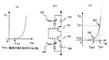
- the block diagram which shows the structure of the transmission circuit in an ultrasonic diagnosing device concerning a 1st Example Diagram for explaining the operation of the transmission circuit according to the first embodiment. Diagram for explaining the operation of the transmission circuit according to the first embodiment.
- the figure which shows the specific structure of the transmission circuit of an ultrasonic diagnosing device concerning a 2nd Example The figure which shows the output waveform of the transmission circuit of the ultrasonic diagnosing device shown in FIG.
- an arbitrary waveform generation unit 1 that generates an arbitrary transmission waveform that is appropriately weighted and amplitude-controlled with a digital signal in the time axis direction and the aperture direction for generating a transmission beam, which are necessary for obtaining a high spatial resolution
- DA converter (DAC) 2 that converts it into an analog signal
- transmission amplification that amplifies this signal to an appropriate amplitude to generate an ultrasonic signal large enough for diagnostic image formation from the transducer described above It is composed of part 3.
- 20 is an input device
- 21 is a transmission method selection signal output from the input device 20.
- the transmission amplification unit 3 includes a signal amplification unit 4 and a current amplification unit 5 that generates a current sufficient to drive the vibrator.
- the signal amplifier 4 and the current amplifier 5 may be realized with the same circuit configuration.
- the signal amplifying unit 4 and the current amplifying unit 5 are functionally different for ease of explanation, they will be considered separately, but this is not the case.
- the current amplifying unit 5 is formed of a FET which is a general current amplifying element. Further, it is assumed that the transmission signal to be handled has both positive and negative poles. For this purpose, the current amplifying unit 5 is simply composed of Pch and Nch, and the totem pole (push) so that the current from the power supply 7 flows to the respective D (drain) and S (source) parts. It is assumed that it is connected to a pull type.
- an FET is known as a switching element, and its characteristic has an exponential relationship between an input voltage and an output current, as shown in FIG.
- the horizontal axis represents the voltage V GS between the G (gate) and S (source) of the FET, which corresponds to the input voltage in this circuit configuration, and the vertical axis represents the corresponding amount of current (I D ).
- V TH the threshold voltage of the FET, and basically shows a point of action where current does not flow at a value smaller than this voltage.
- the minimum operating point of this circuit must be set above V TH, and for that purpose, the FET always has a voltage above V TH. Must be applied in advance. As a result, the FET can respond to any small signal, but even when no signal is input, not less than a constant current flows. This current is hereinafter referred to as a bias current.
- this circuit does not operate when the input signal is small, the value of the lowest input signal that can obtain the output amplitude exceeds the predetermined value, and the input signal control width of the output signal becomes small .
- FIG. 3 shows the input / output characteristics of the transmission amplification unit 3 described above.
- the horizontal axis represents the amplitude value of the input signal
- the vertical axis represents the output signal amplitude value of the transmission amplification unit 3 in FIG.
- the power consumption is reduced as the operating point is lower than the previous point, but the range of the output signal amplitude in the same input signal amplitude range is narrowed, so that the waveform weighting shape that contributes to improving the spatial resolution can be limited.
- the effect is limited. This corresponds to the case indicated by the alternate long and short dash line 9 in FIG. FIG. 3 shows the difference between the control ranges of the output signal amplitudes as Vo_diff.
- the input / output characteristics in the case of a configuration generally called a switching circuit, which will be described later, when the input amplitude exceeds a certain value, the output amplitude becomes a constant value determined by the power source used.
- Vbias105 The bias potential between the gate and source of the FET 101 is represented as Vbias105.
- reference numeral 101 denotes a module for impedance insertion, and a block in which Vbias 105 is connected in series is also an impedance element such as a resistor.
- Vbias 105 has a circuit configuration having a variable power supply function. In FET 101, there is a relationship as shown in FIG. 2C between Vbias 105 and the current flowing through FET 101. As Vgs increases corresponding to Vbias, the current value increases exponentially.
- the value of the current that flows constantly is also 0, but if the input signal does not exceed a certain value (threshold), the FET is turned on. do not do. Although the non-response period is long and the linearity as an amplifier is greatly impaired, the lowest power consumption can be achieved.
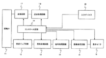
- FIG. 4 shows a configuration example of the entire ultrasonic diagnostic apparatus according to the first embodiment.
- This apparatus configuration includes an ultrasonic probe 11, a transmission processing circuit 18 and a transmission circuit 17 constituting a transmission unit, a reception amplifier circuit 12 and a phasing processing circuit 13 constituting a reception unit, and signal processing.
- a large number of transducers are arranged and used in close contact with the surface of the subject. Each transducer generally converts a pulse wave or continuous wave transmission signal that is input into an ultrasonic wave and emits it to the subject, and receives an electrical signal by receiving the ultrasonic wave reflected from the inside of the subject. It has a function of converting to a wave signal and outputting it.
- each component circuit is subjected to timing control of each part by a control circuit 19 which is a control unit. Further, the control circuit 19 is connected to the input device 20.
- the apparatus user inputs the above-described transmission method selection signal, and inputs a priority for suppressing power consumption or improving spatial resolution by a function described later.
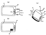
- FIG. 5 is a diagram showing a configuration of a specific example of the input device 20 which is an input device unit.
- 5 (a) and 5 (b) show the configuration when the input device unit is provided on the display monitor 16 in FIG. 4, and
- FIG. 5 (c) shows the configuration on the ultrasonic probe 11 in FIG. Shows a configuration in which an input device unit is provided.
- Input device unit 82 is installed on display monitor 80 in Fig. 5 (a) and slider 83 is used to switch between high spatial resolution operation mode (Res), normal mode (Norm), and low power consumption mode (Pow). Is done.
- the selected mode is displayed on the screen 81 as indicated by 84.
- FIG. 5 (c) shows a case where the switch 86 or 87 is installed on a part of the ultrasonic probe 85 (in this case, the side surface). Even when the switches 86 and 87 are used, the same control as that of the input device unit 82 can be performed.
- FIG. 6 shows a specific configuration of the transmission circuit 17 according to the present embodiment.
- a push-pull circuit using an FET 101 is employed as in FIG.
- the bias of the FET 101 is configured to have a potential difference between the gate of the FET 101 and the power source 103 as shown in FIG. Further, this causes a bias current to flow from the power source 103 to the source / drain of the FET 101.
- the module 104 whose impedance for adjusting the DC current amount, represented by a resistor, is Zs. Put.
- the bias potential 105 is Vbias and the gate-source potential of the FET 101 is Vgs
- the bias current Id is as shown in Expression (1).
- Id (Vbias-Vgs) / Zs --- (1) It can be expressed.
- the steady power consumption Wall of the transmission circuit unit is as shown in Equation (2).
- N indicates the number of transmission circuits per device.
- the operation of the FET 101 is adjusted as described above by adjusting the Vbias indicated by the bias potential 105 or the impedance value indicated by the module 104 by the control signals 26 and 28 from the input device 20.
- the point can be changed.
- the magnitude of the bias potential can be changed, for example, based on an instruction from the input device 20, by applying a DC potential and thereby adjusting the current value flowing through the FET. Not as long.
- the input / output characteristics of this circuit can be changed as indicated by the alternate long and short dash line 9 shown in FIG. This corresponds to the case where the bias current 102 is reduced.
- the bias potential Vbias is 0 V by the control signal 21, that is, the power source 103 and the gate portion of the FET 102 become the same potential in terms of DC.
- an electric element such as a resistor is inserted between the power source 103 and the gate of the FET 102. Further, since no bias current flows, Zs is also short-circuited by the control signal.
- the circuit of FIG. 3 is configured as a so-called switching circuit, and basically outputs a constant output signal determined by the power supply 103 in response to an input signal exceeding the threshold voltage. Since the bias current does not flow, the power consumption is suppressed to the minimum, but the output signal is always constant regardless of the amplitude of the input signal, so the amplitude weighting function necessary for improving the spatial resolution is lost.
- the control signal 21 causes the arbitrary waveform generation unit to output only 0 and VIN, which are simple binary signals. Be changed.
- the DAC 2 can be changed to a simple output configuration that outputs only the most significant bit (MSB), for example.
- the controllable range of transmission amplitude weighting is controlled, and the spatial resolution of the ultrasonic diagnostic image can be changed.
- the negative power supply ( ⁇ HV) may be grounded.
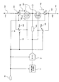
- FIG. 7 shows a circuit configuration that can have, for example, a maximum of ⁇ 2 levels of transmission signal amplitude.
- Each switch circuit is connected to ⁇ HV1 and ⁇ HV2, and their output signals are determined by the power supply value.
- switches 107 and 108 are mounted between each FET 101 and the power supply connected to it. These switches 107 and 108 have the property of turning on when 1 is inputted as a signal and turning off when 0 is inputted.
- the switches 107 and 108 operate independently of the respective FETs 101 or operate in common in a totem pole (push-pull) type having a common FET output.
- Sig1 is input to the switch 107 that determines the operation of the FET 101 connected to ⁇ HV1
- sig2 is input to the switch 108 that determines the operation of the FET 101 connected to ⁇ HV2.
- FIG. 7 shows a case where the circuits using the ⁇ HV1 and ⁇ HV2 power supplies 103 share the same output.
- the output signal is controlled by a value resulting from each power source.
- the first and third waves are controlled by a circuit having ⁇ HV2 as a power source.
- the second wave is controlled by a circuit having ⁇ HV1 as a power source. That is, the waveform weighting effect is achieved, and the above-described spatial resolution improvement can be expected.
- the output signal is as shown in the figure, and the circuit having ⁇ HV2 is not involved in the output signal. Therefore, as shown in the equation (4), the steady power consumption involves only ⁇ HV1 and is lower than that in the equation (3).
- the above-described present invention is particularly useful also in an ultrasonic diagnostic apparatus used as a hand carry unit (HCU).
- HCU hand carry unit
Landscapes
- Engineering & Computer Science (AREA)
- Computer Networks & Wireless Communication (AREA)
- Physics & Mathematics (AREA)
- General Physics & Mathematics (AREA)
- Health & Medical Sciences (AREA)
- Life Sciences & Earth Sciences (AREA)
- Remote Sensing (AREA)
- Radar, Positioning & Navigation (AREA)
- Nuclear Medicine, Radiotherapy & Molecular Imaging (AREA)
- Veterinary Medicine (AREA)
- Heart & Thoracic Surgery (AREA)
- Medical Informatics (AREA)
- Molecular Biology (AREA)
- Surgery (AREA)
- Animal Behavior & Ethology (AREA)
- General Health & Medical Sciences (AREA)
- Public Health (AREA)
- Biomedical Technology (AREA)
- Radiology & Medical Imaging (AREA)
- Pathology (AREA)
- Biophysics (AREA)
- Mechanical Engineering (AREA)
- Human Computer Interaction (AREA)
- Ultra Sonic Daignosis Equipment (AREA)
- Amplifiers (AREA)
- Investigating Or Analyzing Materials By The Use Of Ultrasonic Waves (AREA)
Abstract
Description
まず、超音波診断装置の超音波振動子駆動回路の送信回路を、図1に示すように構成する。
図5の(a)、(b)は、図4の表示モニタ16上に入力デバイス部を設けた場合の構成を示し、同図の(c)は、図4の超音波探触子11上に入力デバイス部を設けた構成を示す。
と表せる。
この条件下における送信回路の入出力特性は図3の実線8に示す値が期待される。
次に、図8の(b)に示すように、±HV2を電源としてもつ回路を、入力デバイス20からの制御により、定常的な消費電力を0として、すなわち使用しないものとする。
よって定常的な電力消費は式(4)に示すとおり、±HV1のみが関与されたものとなり、式(3)に比して低くなる。
以上説明した図7、8の実施例では、正負の電源絶対値がそれぞれ2種類の場合を例に示したが、実際はその限りではなく、より多くの電源をもつ回路で構成されていても、その本質は失われないことは言うまでもない。
Claims (10)
- 超音波を送受信する超音波探触子と、前記超音波探触子に信号を与えて超音波ビームを形成させる送信部と、前記超音波ビームの被検体への送信によって得られる受信信号を受信する受信部と、前記受信信号に基づいて超音波画像を形成する信号処理部と、前記超音波画像を表示する表示部と、前記送信部、前記受信部、前記信号処理部、及び前記表示部を制御する制御部を備える超音波診断装置であって、
前記送信部の動作モードを低消費電力動作モード又は高空間分解能動作モードに設定する設定部を備えることを特徴とする超音波診断装置。 - 請求項1に記載の超音波診断装置であって、
前記設定部は、前記低消費電力モードと前記高空間分解能動作モードの選択を行う入力デバイス部であることを特徴とする超音波診断装置。 - 請求項2に記載の超音波診断装置であって、
前記入力デバイス部は前記表示部上、又は前記超音波探触子の一部の一方に設置されることを特徴とする超音波診断装置。 - 請求項2に記載の超音波診断装置であって、
前記入力デバイス部は、前記低消費電力モードと前記高空間分解能動作モードの間で、複数段階のモードを選択可能であることを特徴とする超音波診断装置。 - 請求の範囲4に記載の超音波診断装置であって、
前記複数段階のモードの選択により、前記送信回路の消費電力量を段階的に制御可能とすることを特徴とした超音波診断装置。 - 請求項1に記載の超音波診断装置であって、
前記送信部は、FETを有し、前記FETのソース・ドレインへのバイアス電流を制御することにより、前記送信部の前記低消費電力動作モードと前記高空間分解能動作モードを選択することを特徴とする超音波診断装置。 - 請求項6に記載の超音波診断装置であって、
入力デバイス部を備え、前記入力デバイス部からの送波方式選択信号に基づき、前記バイアス電流を制御することを特徴とする超音波診断装置。 - 請求項1に記載の超音波診断装置であって、
前記送信部は、第1の電源に接続された第1のFETと、第2の電源に接続された第2のFETを有し、前記第1、第2のFETのソース・ドレインへのバイアス電流を制御することにより、前記送信部の前記低消費電力動作モードと前記高空間分解能動作モードを選択することを特徴とする超音波診断装置。 - 請求項8に記載の超音波診断装置であって、
前記設定部として入力デバイス部を備え、前記入力デバイス部からの送波方式選択信号に基づき、前記バイアス電流を制御することを特徴とする超音波診断装置。 - 請求項9に記載の超音波診断装置であって、
前記第1、第2のFETは、それぞれ前記第1、第2の電源にスイッチを介して接続され、前記スイッチは前記送波信号選択信号によってオンオフ制御されることを特徴とする超音波診断装置。
Priority Applications (2)
| Application Number | Priority Date | Filing Date | Title |
|---|---|---|---|
| JP2010536734A JP5559697B2 (ja) | 2008-11-06 | 2009-10-21 | 超音波診断装置 |
| US13/126,347 US8925386B2 (en) | 2008-11-06 | 2009-10-21 | Ultrasonic diagnostic apparatus |
Applications Claiming Priority (2)
| Application Number | Priority Date | Filing Date | Title |
|---|---|---|---|
| JP2008285573 | 2008-11-06 | ||
| JP2008-285573 | 2008-11-06 |
Publications (1)
| Publication Number | Publication Date |
|---|---|
| WO2010053008A1 true WO2010053008A1 (ja) | 2010-05-14 |
Family
ID=42152817
Family Applications (1)
| Application Number | Title | Priority Date | Filing Date |
|---|---|---|---|
| PCT/JP2009/068092 Ceased WO2010053008A1 (ja) | 2008-11-06 | 2009-10-21 | 超音波診断装置 |
Country Status (3)
| Country | Link |
|---|---|
| US (1) | US8925386B2 (ja) |
| JP (1) | JP5559697B2 (ja) |
| WO (1) | WO2010053008A1 (ja) |
Cited By (2)
| Publication number | Priority date | Publication date | Assignee | Title |
|---|---|---|---|---|
| JP2012161555A (ja) * | 2011-02-09 | 2012-08-30 | Fujifilm Corp | 超音波診断装置および方法 |
| JP2021508584A (ja) * | 2018-01-02 | 2021-03-11 | コーニンクレッカ フィリップス エヌ ヴェKoninklijke Philips N.V. | 高出力マイクロビームフォーマ超音波トランスデューサプローブ |
Families Citing this family (6)
| Publication number | Priority date | Publication date | Assignee | Title |
|---|---|---|---|---|
| JP5330431B2 (ja) * | 2011-03-11 | 2013-10-30 | 富士フイルム株式会社 | 超音波プローブおよび超音波診断装置 |
| JP2012217618A (ja) * | 2011-04-08 | 2012-11-12 | Fujifilm Corp | 超音波診断装置 |
| JP5831000B2 (ja) * | 2011-07-21 | 2015-12-09 | ソニー株式会社 | 信号処理装置、制御方法、並びに信号処理システムおよび方法 |
| US10667790B2 (en) | 2012-03-26 | 2020-06-02 | Teratech Corporation | Tablet ultrasound system |
| US9877699B2 (en) | 2012-03-26 | 2018-01-30 | Teratech Corporation | Tablet ultrasound system |
| KR102551252B1 (ko) | 2015-11-11 | 2023-07-05 | 삼성메디슨 주식회사 | 초음파 진단 장치 및 그 동작방법 |
Citations (10)
| Publication number | Priority date | Publication date | Assignee | Title |
|---|---|---|---|---|
| JPH0556973A (ja) * | 1991-09-02 | 1993-03-09 | Toshiba Corp | 超音波血流イメージング装置 |
| JP2001269336A (ja) * | 2000-03-24 | 2001-10-02 | Toshiba Corp | 超音波診断装置 |
| JP2002065672A (ja) * | 2000-09-01 | 2002-03-05 | Hitachi Medical Corp | 超音波診断装置 |
| JP2003235842A (ja) * | 2002-02-18 | 2003-08-26 | Aloka Co Ltd | 超音波診断装置 |
| JP2004073883A (ja) * | 2003-10-17 | 2004-03-11 | Aloka Co Ltd | 超音波診断装置の送信回路 |
| JP2005152450A (ja) * | 2003-11-27 | 2005-06-16 | Olympus Corp | 超音波観測装置 |
| JP2005192868A (ja) * | 2004-01-08 | 2005-07-21 | Matsushita Electric Ind Co Ltd | 超音波診断装置 |
| JP2006000287A (ja) * | 2004-06-16 | 2006-01-05 | Fuji Photo Film Co Ltd | 超音波送受信装置 |
| JP2006122449A (ja) * | 2004-10-29 | 2006-05-18 | Hitachi Medical Corp | 超音波診断装置 |
| JP2006217942A (ja) * | 2005-02-08 | 2006-08-24 | Fuji Photo Film Co Ltd | 超音波撮像装置 |
Family Cites Families (8)
| Publication number | Priority date | Publication date | Assignee | Title |
|---|---|---|---|---|
| JP3614075B2 (ja) * | 2000-03-16 | 2005-01-26 | 松下電器産業株式会社 | 超音波プローブ |
| US6511429B1 (en) * | 2000-08-17 | 2003-01-28 | Mayo Foundation For Medical Education And Research | Ultrasonic methods and systems for reducing fetal stimulation |
| JP2003339700A (ja) * | 2002-05-27 | 2003-12-02 | Toshiba Medical System Co Ltd | 超音波プローブ及び超音波診断装置 |
| JP2003175035A (ja) | 2003-01-07 | 2003-06-24 | Aloka Co Ltd | 超音波診断装置 |
| US6836159B2 (en) * | 2003-03-06 | 2004-12-28 | General Electric Company | Integrated high-voltage switching circuit for ultrasound transducer array |
| JP4643214B2 (ja) | 2004-10-01 | 2011-03-02 | 株式会社東芝 | 超音波プローブ及び超音波診断装置 |
| US7775979B2 (en) * | 2005-06-29 | 2010-08-17 | General Electric Company | Transmit and receive interface array for highly integrated ultrasound scanner |
| US8096949B2 (en) * | 2008-07-02 | 2012-01-17 | U-Systems, Inc. | User interface for ultrasound mammographic imaging |
-
2009
- 2009-10-21 JP JP2010536734A patent/JP5559697B2/ja not_active Expired - Fee Related
- 2009-10-21 WO PCT/JP2009/068092 patent/WO2010053008A1/ja not_active Ceased
- 2009-10-21 US US13/126,347 patent/US8925386B2/en not_active Expired - Fee Related
Patent Citations (10)
| Publication number | Priority date | Publication date | Assignee | Title |
|---|---|---|---|---|
| JPH0556973A (ja) * | 1991-09-02 | 1993-03-09 | Toshiba Corp | 超音波血流イメージング装置 |
| JP2001269336A (ja) * | 2000-03-24 | 2001-10-02 | Toshiba Corp | 超音波診断装置 |
| JP2002065672A (ja) * | 2000-09-01 | 2002-03-05 | Hitachi Medical Corp | 超音波診断装置 |
| JP2003235842A (ja) * | 2002-02-18 | 2003-08-26 | Aloka Co Ltd | 超音波診断装置 |
| JP2004073883A (ja) * | 2003-10-17 | 2004-03-11 | Aloka Co Ltd | 超音波診断装置の送信回路 |
| JP2005152450A (ja) * | 2003-11-27 | 2005-06-16 | Olympus Corp | 超音波観測装置 |
| JP2005192868A (ja) * | 2004-01-08 | 2005-07-21 | Matsushita Electric Ind Co Ltd | 超音波診断装置 |
| JP2006000287A (ja) * | 2004-06-16 | 2006-01-05 | Fuji Photo Film Co Ltd | 超音波送受信装置 |
| JP2006122449A (ja) * | 2004-10-29 | 2006-05-18 | Hitachi Medical Corp | 超音波診断装置 |
| JP2006217942A (ja) * | 2005-02-08 | 2006-08-24 | Fuji Photo Film Co Ltd | 超音波撮像装置 |
Cited By (3)
| Publication number | Priority date | Publication date | Assignee | Title |
|---|---|---|---|---|
| JP2012161555A (ja) * | 2011-02-09 | 2012-08-30 | Fujifilm Corp | 超音波診断装置および方法 |
| JP2021508584A (ja) * | 2018-01-02 | 2021-03-11 | コーニンクレッカ フィリップス エヌ ヴェKoninklijke Philips N.V. | 高出力マイクロビームフォーマ超音波トランスデューサプローブ |
| JP7292305B2 (ja) | 2018-01-02 | 2023-06-16 | コーニンクレッカ フィリップス エヌ ヴェ | 高出力マイクロビームフォーマ超音波トランスデューサプローブ |
Also Published As
| Publication number | Publication date |
|---|---|
| JP5559697B2 (ja) | 2014-07-23 |
| US20110203374A1 (en) | 2011-08-25 |
| US8925386B2 (en) | 2015-01-06 |
| JPWO2010053008A1 (ja) | 2012-04-05 |
Similar Documents
| Publication | Publication Date | Title |
|---|---|---|
| JP5559697B2 (ja) | 超音波診断装置 | |
| JP4934631B2 (ja) | マルチレベル送信機を備える再構成可能なアレイ | |
| JP5238438B2 (ja) | 超音波診断装置 | |
| JP5384491B2 (ja) | 超音波診断装置 | |
| JP5436534B2 (ja) | 超音波送受信回路、超音波診断装置 | |
| JP6005956B2 (ja) | 超音波診断装置 | |
| JP5804949B2 (ja) | 超音波診断装置 | |
| JP5260068B2 (ja) | 探知装置および探知方法 | |
| CN111050665B (zh) | 超声波成像装置、超声波探针以及发送装置 | |
| WO2010103747A1 (ja) | 超音波診断装置 | |
| JP3492581B2 (ja) | 超音波診断装置用送信回路 | |
| WO2010101105A1 (ja) | 超音波診断装置、及び超音波探触子、超音波診断方法 | |
| JP5718152B2 (ja) | 超音波探触子、超音波診断装置 | |
| JPWO2010114086A1 (ja) | 超音波診断装置、及び送波信号発生回路 | |
| JP2008188321A (ja) | 超音波診断装置 | |
| JP6301114B2 (ja) | 超音波診断装置 | |
| JP2006122449A (ja) | 超音波診断装置 | |
| JP2004008684A (ja) | 超音波診断装置 | |
| JPH11342127A (ja) | 超音波診断装置用送信回路 | |
| JP4313905B2 (ja) | パルス増幅器及びそれを用いた超音波診断装置 | |
| JP2002065672A (ja) | 超音波診断装置 | |
| JP3857676B2 (ja) | 超音波診断装置の送信回路 | |
| JP2007111257A (ja) | 超音波診断装置および超音波プローブ | |
| JP2004089512A (ja) | 超音波診断装置 | |
| US11013496B2 (en) | Ultrasound diagnostic apparatus |
Legal Events
| Date | Code | Title | Description |
|---|---|---|---|
| 121 | Ep: the epo has been informed by wipo that ep was designated in this application |
Ref document number: 09824708 Country of ref document: EP Kind code of ref document: A1 |
|
| ENP | Entry into the national phase |
Ref document number: 2010536734 Country of ref document: JP Kind code of ref document: A |
|
| WWE | Wipo information: entry into national phase |
Ref document number: 13126347 Country of ref document: US |
|
| NENP | Non-entry into the national phase |
Ref country code: DE |
|
| 122 | Ep: pct application non-entry in european phase |
Ref document number: 09824708 Country of ref document: EP Kind code of ref document: A1 |