WO2010050562A1 - 処理制御ユニット、処理実行ユニット、情報処理装置、制御方法、制御プログラム、および制御プログラムを記録したコンピュータ読み取り可能な記録媒体 - Google Patents
処理制御ユニット、処理実行ユニット、情報処理装置、制御方法、制御プログラム、および制御プログラムを記録したコンピュータ読み取り可能な記録媒体 Download PDFInfo
- Publication number
- WO2010050562A1 WO2010050562A1 PCT/JP2009/068609 JP2009068609W WO2010050562A1 WO 2010050562 A1 WO2010050562 A1 WO 2010050562A1 JP 2009068609 W JP2009068609 W JP 2009068609W WO 2010050562 A1 WO2010050562 A1 WO 2010050562A1
- Authority
- WO
- WIPO (PCT)
- Prior art keywords
- unit
- execution
- main
- control unit
- display device
- Prior art date
- Legal status (The legal status is an assumption and is not a legal conclusion. Google has not performed a legal analysis and makes no representation as to the accuracy of the status listed.)
- Ceased
Links
Images









Classifications
-
- G—PHYSICS
- G06—COMPUTING OR CALCULATING; COUNTING
- G06F—ELECTRIC DIGITAL DATA PROCESSING
- G06F3/00—Input arrangements for transferring data to be processed into a form capable of being handled by the computer; Output arrangements for transferring data from processing unit to output unit, e.g. interface arrangements
- G06F3/01—Input arrangements or combined input and output arrangements for interaction between user and computer
- G06F3/03—Arrangements for converting the position or the displacement of a member into a coded form
- G06F3/041—Digitisers, e.g. for touch screens or touch pads, characterised by the transducing means
- G06F3/0412—Digitisers structurally integrated in a display
-
- G—PHYSICS
- G06—COMPUTING OR CALCULATING; COUNTING
- G06F—ELECTRIC DIGITAL DATA PROCESSING
- G06F11/00—Error detection; Error correction; Monitoring
- G06F11/22—Detection or location of defective computer hardware by testing during standby operation or during idle time, e.g. start-up testing
- G06F11/2284—Detection or location of defective computer hardware by testing during standby operation or during idle time, e.g. start-up testing by power-on test, e.g. power-on self test [POST]
-
- G—PHYSICS
- G06—COMPUTING OR CALCULATING; COUNTING
- G06F—ELECTRIC DIGITAL DATA PROCESSING
- G06F3/00—Input arrangements for transferring data to be processed into a form capable of being handled by the computer; Output arrangements for transferring data from processing unit to output unit, e.g. interface arrangements
- G06F3/01—Input arrangements or combined input and output arrangements for interaction between user and computer
- G06F3/03—Arrangements for converting the position or the displacement of a member into a coded form
- G06F3/041—Digitisers, e.g. for touch screens or touch pads, characterised by the transducing means
- G06F3/042—Digitisers, e.g. for touch screens or touch pads, characterised by the transducing means by opto-electronic means
Definitions
- the present invention relates to a process control unit, a process execution unit, an information processing apparatus, a control method, a control program, and a computer-readable recording medium that records the control program.
- a sub display device including a sub display is provided separately from the main display device including the main display, and the sub display device has a function that enables mouse pointing operation, numeric keypad input operation, menu screen display, and the like. .
- Patent Documents 1 to 4 disclose conventional techniques related to a notebook PC equipped with such a sub display device.
- BIOS Basic Input Input Output System
- the BIOS first displays the sub display device and its controller in a displayable state, and displays the password input request on the sub display device.
- a technique for performing control is disclosed.
- Patent Document 2 discloses a technique for securing a display area near a mouse pointer displayed on a main display device and displaying a switching menu screen handled by a sub display device in the display area.
- Patent Document 3 discloses a technique for displaying a screen image of the entire desktop including the main operation screen displayed on the main display device on the sub display device as an operation screen for instructing the position of the mouse pointer by a touch operation. .
- Patent Document 4 when a function button included in a notebook PC is operated, a menu for selecting a function is displayed on the sub display device, and when the user operates the sub display device and selects a numeric keypad from the menu, A technique for displaying an operable numeric keypad on a sub display device is disclosed.
- a control unit (specifically, a CPU (central processing unit)) is provided in the main display device, and the sub display device is controlled by the control unit.
- the status (status) of the failure may be presented to the user. There is a problem that you can not.
- an OS Oleting System
- the main display device starts when the sub display device displays that fact or there is no fault in the startup process. Cannot be performed from the sub display device.
- each of the main display device and the sub display device includes a control unit, and the operation status of the main display device is referred to from the sub display device, or according to the operation status of the main display device. It is conceivable to control the main display device from the sub display device.
- a notebook PC is not disclosed in Patent Documents 1 to 4 described above.
- the present invention has been made in view of the above-described problems, and an object thereof is to be executed by the main apparatus in an information processing apparatus having a main apparatus and a sub apparatus according to the execution status of processing in the main apparatus.
- An object of the present invention is to provide a process control unit, a process execution unit, an information processing apparatus, a control method, a control program, and a computer-readable recording medium on which the control program is recorded.
- the process control unit generates execution status information indicating the execution status while executing the first processing, and performs the second processing after the first processing.
- a process control unit that is communicable with a process execution unit to be executed and is operable independently of the process execution unit, and acquires the generated execution status information from the process execution unit and the acquisition
- the execution status determining means for determining whether or not the executed status information is a predetermined value
- the execution status determining means determines that the acquired execution status information is the predetermined value
- the processing execution unit Execution designation means for designating the process execution unit so that any one of a plurality of executable candidate processes is executed as the second process. It is set to.
- control method of the processing control unit is a process for generating execution status information indicating the execution status while executing the first processing, and executing the second processing after the first processing.
- a method for controlling a processing control unit that is communicable with an execution unit and operable independently of the process execution unit, wherein the generated execution status information is acquired from the process execution unit and the acquisition is performed.
- An execution designation step that designates the process execution unit so that any one of a plurality of candidate processes that can be executed in the process is executed as the second process. It is characterized in Mukoto.
- any one of the plurality of candidate processes is designated as a second process executed after the first process in the process execution unit. be able to.
- the process control unit determines one of a plurality of candidate processes that can be executed by the process execution unit as the second process. Can be specified as
- the process control unit can control the subsequent process (second process) executed by the process execution unit according to the execution status of the preceding process (first process) in the process execution unit.
- the execution status can be changed from the process control unit without depending on the execution result of the preceding process (first process) in the process execution unit. Can be confirmed. Therefore, even if some trouble occurs during the preceding process (first process) in the process execution unit, it is possible to confirm the execution status of the process in the process execution unit from the process control unit.
- the process execution unit generates execution status information indicating the execution status while executing the first process, and after the first process, A process execution unit that communicates with the process control unit and executes any one of a plurality of executable candidate processes as the second process, and the second process from the process control unit that can read the execution status information And an execution control means for executing the designated second process after the first process.
- the method for controlling a process execution unit generates execution status information indicating the execution status while executing the first process, and can be executed by the own unit after the first process.
- the second process designated by the process control unit can be executed.
- the process execution unit can execute the second process in response to an instruction from the process control unit.
- the process execution unit can execute the subsequent process (second process) designated by the process control unit in accordance with the execution status of the preceding process (first process).
- the execution status can be changed from the process control unit without depending on the execution result of the preceding process (first process) in the process execution unit. Can be confirmed. Therefore, even if some trouble occurs during the preceding process (first process) in the process execution unit, it is possible to confirm the execution status of the process in the process execution unit from the process control unit.
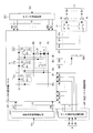
- FIG. 1 is a block diagram illustrating a detailed configuration of a main display device and a sensor-equipped sub display device according to an embodiment of the present invention.
- (A) of the figure is a schematic diagram showing a specific example of the two-screen display device, and
- (A) of the figure is a schematic diagram showing how the position touched by the user is detected by detecting the reflected image, and (b) of the figure shows that the user touches by detecting the shadow image. It is a schematic diagram which shows a mode that the performed position is detected. It is a block diagram which shows the principal part structure of the said main display apparatus and a sub display apparatus with a sensor. It is a block diagram which shows the more detailed structure of the display / light sensor part with which the said sub display apparatus with a sensor is equipped, a display / light sensor circuit control part, and a data processing part. It is a block diagram which shows the structural example of the display part with which the said sub display apparatus with a sensor is equipped, and a display circuit control part.
- FIGS. 1 to 17 An embodiment of the present invention will be described with reference to FIGS. 1 to 17 as follows.
- the outline of the present invention is that when the execution state of the first process executed by the main display device (process execution unit) 210 is a predetermined state, the second process that can be executed by the main display device 210 is displayed as a main display. It is specified from the sub display device with a sensor (processing control unit) 230 that can operate independently of the device.
- an OS Operating System
- an OS that can be executed on the main display device 210 is executed particularly when the execution status of the basic input output system (BIOS) immediately after the main display device 210 is turned on is a predetermined status.
- BIOS basic input output system
- a case where the activation process is designated from the sub display device with sensor 230 will be described as an example.
- the main display device 210 is installed with a plurality of OSs that can be executed by the device itself, and any one of them is activated (in a multi-boot state).
- the two-screen display device 200 includes a main display device 210 including a liquid crystal panel 311 capable of displaying data, and a sensor built-in liquid crystal panel 301 (described later) capable of detecting an image of a nearby object in addition to displaying data.
- a main display device 210 including a liquid crystal panel 311 capable of displaying data, and a sensor built-in liquid crystal panel 301 (described later) capable of detecting an image of a nearby object in addition to displaying data.
- This is a device having a sub-display device 230 with a sensor.
- the main display device 210 and the sensor-equipped sub display device 230 are detachable.
- the sensor-equipped sub-display device 230 is mounted on the main display device 210, it becomes possible to perform wired communication with each other, and by transmitting an “inter-device command” to the partner device, the partner device Can be controlled. Details of the inter-device command will be described later.
- the main display device 210 and the sensor-equipped sub display device 230 each include a control unit that controls the device itself. Therefore, in a state where the main display device 210 and the sensor-equipped sub display device 230 are separated from each other, each can operate independently.
- FIG. 2A is a schematic diagram illustrating a specific example of the two-screen display device 200.
- a notebook PC Personal Computer
- a portion other than the sensor-equipped sub display device 230 corresponds to the main display device 210.
- the state shown in FIG. 2A is a state in which the sub display device with sensor 230 is mounted inside the main display device 210.
- the portion corresponding to the touch pad of the main display device 210 is transparent, and the user can operate the sensor built-in liquid crystal panel 301 of the sub display device with sensor 230 mounted inside.
- FIG. 2B is a schematic diagram showing a state in which the sensor-equipped sub display device 230 is taken out from the main display device 210 and separated from the notebook PC shown in FIG.
- the main display device 210 and the sensor-equipped sub-display device 230 can each operate alone.
- the main display device 210 can operate as a notebook PC having no touch pad function. It is.
- the sensor-equipped sub-display device 230 can operate as, for example, a remote controller including the sensor built-in liquid crystal panel 301 or a PDA (Personal Digital Assistant).
- the sensor built-in liquid crystal panel 301 included in the sensor-equipped sub-display device 230 is a liquid crystal panel capable of detecting an image of a nearby object in addition to displaying data.
- the image detection of the object is, for example, detection of a position pointed (touched) by the user with a finger or a pen, or reading (scanning) of an image of a printed material or the like.
- the device used for display is not limited to a liquid crystal panel, and may be an organic EL (Electro Luminescence) panel or the like.
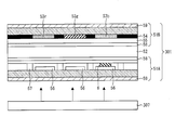
- FIG. 3 is a diagram schematically showing a cross section of the sensor built-in liquid crystal panel 301.
- the sensor built-in liquid crystal panel 301 described here is an example, and any structure can be used as long as the display surface and the reading surface are shared.
- the sensor built-in liquid crystal panel 301 includes an active matrix substrate 51A disposed on the back surface side and a counter substrate 51B disposed on the front surface side, and has a structure in which a liquid crystal layer 52 is sandwiched between these substrates. is doing.
- the active matrix substrate 51A is provided with a pixel electrode 56, a data signal line 57, an optical sensor circuit 32 (not shown), an alignment film 58, a polarizing plate 59, and the like.
- the counter substrate 51B is provided with color filters 53r (red), 53g (green), 53b (blue), a light shielding film 54, a counter electrode 55, an alignment film 58, a polarizing plate 59, and the like.
- a backlight 307 is provided on the back surface of the sensor built-in liquid crystal panel 301.
- the photodiode 6 included in the optical sensor circuit 32 is provided in the vicinity of the pixel electrode 56 provided with the blue color filter 53b, but is not limited to this configuration. It may be provided in the vicinity of the pixel electrode 56 provided with the red color filter 53r, or may be provided in the vicinity of the pixel electrode 56 provided with the green color filter 53g.
- FIGS. 4A and 4B a case where the user touches the sensor built-in liquid crystal panel 301 with a finger or a pen is taken as an example, and the touched position is detected. Two types of methods are described.
- FIG. 4 is a schematic diagram showing how the position touched by the user is detected by detecting the reflected image.
- the optical sensor circuit 32 including the photodiode 6 detects the light 63 reflected by the object 64 such as a finger. Thereby, the reflected image of the target object 64 can be detected.
- the sensor built-in liquid crystal panel 301 can detect the touched position by detecting the reflected image.
- FIG. 4B is a schematic diagram showing a state in which a position touched by the user is detected by detecting a shadow image.
- the optical sensor circuit 32 including the photodiode 6 detects external light 61 transmitted through the counter substrate 51B and the like.
- the incident of the external light 61 is hindered, so that the amount of light detected by the optical sensor circuit 32 is reduced.
- a shadow image of the object 62 can be detected.
- the sensor built-in liquid crystal panel 301 can also detect a touched position by detecting a shadow image.
- the photodiode 6 may detect reflected light (shadow image) of the light emitted from the backlight 307, or may detect a shadow image caused by external light. Further, the two types of detection methods may be used in combination to detect both a shadow image and a reflected image at the same time.
- FIG. 5 is a block diagram illustrating a main configuration of the main display device 210 and the sub display device with sensor 230.
- the sensor-equipped sub-display device 230 includes a display / light sensor unit 330, a display / light sensor circuit control unit 630, a data processing unit 730, a sub-side main control unit 830, a storage unit 931, a primary storage unit 932, A communication control unit 933, a wired communication unit 934, a short-range wireless communication unit 935, an electric field strength detection unit 936, a battery 937, and a power supply switching unit 938 are provided.
- the display / light sensor unit 330 is a so-called light sensor built-in liquid crystal display device.
- the display / light sensor unit 330 includes a sensor built-in liquid crystal panel 301, a backlight 307, and a peripheral circuit 309 for driving them. A detailed configuration of the display / light sensor unit 330 will be described later.
- the display / light sensor circuit control unit 630 has a function as a device driver that controls the peripheral circuit 309 of the display / light sensor unit 330.
- a detailed configuration of the display / light sensor circuit control unit 630 will be described later.
- the data processing unit 730 has a function as middleware that gives an instruction to the display / light sensor circuit control unit 630 based on the “in-sub display device command” received from the sub-side main control unit 830. .
- a detailed configuration of the data processing unit 730 will be described later. Details of the sub display device commands will also be described later.
- the sub-side main control unit 830 controls the operation of each unit included in the sensor-equipped sub display device 230.
- the sub-side main control unit 830 reads various programs stored in the storage unit 931, controls each unit of the sensor-equipped sub display device 230, and implements various functions included in the sensor-equipped sub display device 230.
- the sub-side main control unit 830 causes the data processing unit 730 to display the display data on the sensor built-in liquid crystal panel 301 and to scan the object in the sensor built-in liquid crystal panel 301.
- “data type” is designated for the command within the sub display device, at least one of the whole image data, the partial image data, and the coordinate data is sent as a response to the command within the sub display device.
- the sub-side main control unit 830 receives control from the main display device 210. Specifically, the inter-device command transmitted from the main-side main control unit 810 of the main display device 210 is received, and one of the following (1) to (3) is selected according to the type of the received inter-device command. The process shown is executed.
- the sub-side The main control unit 830 converts the received scan command into a sub display device command, and transmits the converted sub display device command to the data processing unit 730.
- the above conversion is performed by removing a “0th” field (described later) from the scan command.
- the sub-side main control unit 830 receives at least one of the whole image data, the partial image data, and the coordinate data from the data processing unit 730 as a response to the command within the sub-display device after the conversion.
- the received data is transmitted to the main main control unit 810.
- the sub-side main control unit 830 generates display data based on the information specified in the display command, and transmits the generated display data to the data processing unit 730.
- the sub-side main control unit 830 is designated as the processing command.
- the predetermined processing is executed.
- the predetermined processing executed by the sub-side main control unit 830 includes, for example, character recognition processing and image processing for image data obtained from the data processing unit 730, and communication using the communication control unit 933 of the sensor-equipped sub display device 230.
- This is an execution process of various applications, middleware, and the like included in the sensor-equipped sub display device 230 such as a connection process and a file transfer process.
- the sub-side main control unit 830 instructs the main display device 210 to execute a predetermined process. Specifically, an inter-device command as a processing command is transmitted to the main side main control unit 810 of the main display device 210.
- the predetermined processing executed by the main main control unit 810 includes, for example, OS (Operating System) startup processing of the main display device 210, communication connection processing using the communication control unit 913 of the main display device 210, and file transfer processing And execution processing of various applications, middleware, and the like that the main display device 210 has.
- OS Operating System
- the display / light sensor circuit control unit 630, the data processing unit 730, and the sub-side main control unit 830 can be configured by a CPU (Central Processing Unit) and a memory, respectively. Further, the data processing unit 730 may be configured by a circuit such as an ASIC (application specific circuit).
- a CPU Central Processing Unit
- ASIC application specific circuit
- the storage unit 931 reads (1) the control program for each unit, (2) the OS program, (3) the application program, and (4) the program executed by the sub-side main control unit 830. Records various data.
- the storage unit 931 is configured by a nonvolatile storage device such as a flash memory.
- the primary storage unit 932 is configured by a volatile storage device such as a RAM (Random Access Memory), and temporarily stores data in the process of executing the various programs described above by the sub-side main control unit 830. Used as a work area.
- a volatile storage device such as a RAM (Random Access Memory)
- the communication control unit 933 allows the sensor-equipped sub display device 230 to communicate with either the wired communication unit 934 for communicating with the main display device 210, and the main display device 210 or an external device (not shown).
- the short-range wireless communication unit 935 is controlled.
- the communication control unit 933 transmits an inter-device command and various data transmitted from the main display device 210 via either the wired communication unit 934 or the short-range wireless communication unit 935 to the sub-side main control unit 830. . Also, the communication control unit 933 sends inter-device commands and various data transmitted from the sub-side main control unit 830 in response to an instruction from the sub-side main control unit 830, and the wired communication unit 934 and the short-range wireless communication unit 935. Is transmitted to the main display device 210.
- the communication control unit 933 exchanges various data with the external device via the short-range wireless communication unit 935.
- the wired communication unit 934 can be connected to the wired communication unit 914 of the main display device 210.
- USB universal serial bus
- the wired communication unit 934 can transmit and receive signals to and from the wired communication unit 914 of the main display device 210 using the communication line, and the wired communication of the main display device 210 using the power line. Power can be supplied from the unit 914. When the power supply is received from the wired communication unit 914 of the main display device 210, the wired communication unit 934 supplies power to the power supply switching unit 938.
- the short-range wireless communication unit 935 can communicate with each other using a wireless communication path formed with the short-range wireless communication unit 915 of the main display device 210 and with an external device. Yes.
- Bluetooth registered trademark
- the short-range wireless communication unit 935 is a communication unit that can transmit and receive signals by Bluetooth communication.
- the wireless communication path is not particularly limited as long as it can transmit and receive signals, and IEEE802.11 wireless, ZigBee (registered trademark), or the like may be applied.
- the electric field strength detection unit 936 detects the strength of a signal received by the short-range wireless communication unit 935 (RSSI (Received Signal Strength Strength): received electric field strength) in response to an instruction from the sub-side main control unit 830. To do. Then, the detection result is transmitted to the sub-side main control unit 830.
- RSSI Receiveived Signal Strength Strength
- the power supply switching unit 938 supplies the power to the respective units included in the sensor-equipped sub display device 230 from the main display device 210. Supply the power that is.
- the power supply switching unit 938 supplies the power of the battery 937 to each unit included in the sensor-equipped sub display device 230. .
- the main display device 210 includes a display unit 310, a display circuit control unit 610, a display data processing unit 710, a main side main control unit 810, a storage unit 911, a primary storage unit 912, a communication control unit 913, and wired communication.
- the display unit 310 is for displaying data, and includes a liquid crystal panel 311, a backlight 317, and a peripheral circuit 319 for driving them.
- the display circuit control unit 610 has a function as a device driver that controls the peripheral circuit 319.
- the display data processing unit 710 has a function as middleware that gives an instruction to the display circuit control unit 610 based on the display data received from the main main control unit 810.
- the display unit 310, the display circuit control unit 610, and the display data processing unit 710 can be configured using a generally known technique.
- the main side main control unit 810 controls the operation of each unit included in the main display device 210.
- the main main control unit 810 reads various programs stored in the storage unit 911, controls each unit of the main display device 210, and realizes various functions included in the main display device 210.
- the main side main control unit 810 transmits an inter-device command to the sub side main control unit 830 of the sensor-equipped sub display device 230, and causes the sensor-equipped sub display device 230 to execute predetermined processing.
- data type (described later) is specified for a scan command that is one of the inter-device commands, at least one of whole image data, partial image data, and coordinate data is returned as a response to the command. Is received from the sub-side main control unit 830.
- the main main control unit 810 receives a processing command that is one of the inter-device commands from the sub-side main control unit 830 of the sensor-equipped sub display device 230, and performs a predetermined process specified in the received inter-device command. (OS startup processing, execution processing of various applications, middleware, etc.) is performed.
- the display circuit control unit 610, the display data processing unit 710, and the main side main control unit 810 can each be configured with a CPU, a memory, and the like.
- the storage unit 911 reads (1) the control program for each unit, (2) the OS program, (3) the application program, and (4) the program executed by the main-side main control unit 810. Records various data.
- the storage unit 911 is configured by a nonvolatile storage device such as a flash memory.
- the primary storage unit 912 is configured by a volatile storage device such as a RAM, and serves as a work area for temporarily storing data in the course of executing the above-described various programs by the main main control unit 810. used.
- the communication control unit 913 is a short-range wireless communication for the main display device 210 to communicate with the wired communication unit 914 for communicating with the sensor-equipped sub-display device 230, the sensor-equipped sub-display device 230, and an external device (not shown).
- Control unit 915 and wired / wireless network communication unit 916 for communicating with an external device (not shown).
- the communication control unit 913 sends inter-device commands and various data transmitted from the sensor-equipped sub display device 230 via either the wired communication unit 914 or the short-range wireless communication unit 915 to the main main control unit 810. Send.
- the communication control unit 913 receives inter-device commands and various data transmitted from the main main control unit 810 in response to an instruction from the main main control unit 810, the wired communication unit 914, and the short-range wireless communication unit 915. Is transmitted to the sensor-equipped sub-display device 230.
- the communication control unit 933 exchanges various data with an external device via either the short-range wireless communication unit 935 or the wired / wireless network communication unit 916.
- the wired communication unit 914 can be connected to the wired communication unit 934 of the sensor-equipped sub display device 230.
- the wired communication unit 914 and the wired communication unit 934 of the sensor-equipped sub display device 230 Assumes a USB connection.
- the short-range wireless communication unit 915 is configured to be able to communicate with each other using a wireless communication path formed between the short-range wireless communication unit 935 of the sensor-equipped sub display device 230 and an external device. It is assumed that Bluetooth communication is applied to the wireless communication path. In other words, the short-range wireless communication unit 915 is a communication unit that can transmit and receive signals by Bluetooth communication.
- the wired / wireless network communication unit 916 is configured to be communicably connected to an external communication network, and performs communication with an external device.
- the communication network is not particularly limited.
- the Internet intranet, extranet, LAN, ISDN, VAN, CATV communication network, virtual private network, telephone line network, mobile communication network, satellite communication. A net or the like is available.
- the power source 917 supplies power to each unit included in the main display device 210.
- the wired communication unit 914 is connected to the wired communication unit 934 of the sensor-equipped sub display device 230, power is also supplied to the sensor-equipped sub display device 230 via the wired communication unit 914.
- the power can be turned on / off by the user operating the power switch 922.
- the operation unit 919 receives an input operation of the user of the main display device 210.
- the operation unit 919 includes, for example, an input device such as a keyboard 920, a switch, a mouse, and a remote controller. Then, the operation unit 919 generates a control signal corresponding to the input operation of the user of the main display device 210, and transmits the generated control signal to the main side main control unit 810.
- a hinge switch 921 for detecting the open / closed state of the casing a power switch 922 for switching on / off of the power
- a hardware switch such as a user switch 923 to which a function is assigned is assumed.
- the main display device 210 includes an audio output unit 924 such as a speaker for outputting audio and an audio input unit 925 such as a microphone for inputting an audio signal.
- an audio output unit 924 such as a speaker for outputting audio
- an audio input unit 925 such as a microphone for inputting an audio signal.
- FIG. 6 is a block diagram showing more detailed configurations of the display / light sensor unit 330, the display / light sensor circuit control unit 630, and the data processing unit 730.
- the display / light sensor unit 330 includes a sensor built-in liquid crystal panel 301, a backlight 307, and a peripheral circuit 309 for driving them.
- the sensor built-in liquid crystal panel 301 includes a plurality of pixel circuits 31 and optical sensor circuits 32 arranged in a matrix. The detailed configuration of the sensor built-in liquid crystal panel 301 will be described later.
- Peripheral circuit 309 includes a liquid crystal panel drive circuit 304, an optical sensor drive circuit 305, a signal conversion circuit 306, and a backlight drive circuit 308.
- the liquid crystal panel drive circuit 304 outputs a control signal (G) and a data signal (S) in accordance with the timing control signal (TC1) and the data signal (D) from the liquid crystal panel control unit 601 of the display / light sensor circuit control unit 630. In this case, the pixel circuit 31 is driven. Details of the driving method of the pixel circuit 31 will be described later.
- the optical sensor driving circuit 305 is a circuit that drives the optical sensor circuit 32 by applying a voltage to the signal line (R) in accordance with the timing control signal (TC2) from the sensor control unit 602 of the display / optical sensor circuit control unit 630. is there. Details of the driving method of the optical sensor circuit 32 will be described later.
- the signal conversion circuit 306 is a circuit that converts the sensor output signal (SS) output from the optical sensor circuit 32 into a digital signal (DS) and transmits the converted signal to the sensor control unit 602.
- the backlight 307 includes a plurality of white LEDs (Light Emitting Diodes) and is disposed on the back surface of the sensor built-in liquid crystal panel 301. When a power supply voltage is applied from the backlight drive circuit 308, the backlight 307 is turned on and irradiates the sensor built-in liquid crystal panel 301 with light. Note that the backlight 307 is not limited to white LEDs, and may include LEDs of other colors. Further, the backlight 307 may include, for example, a cold cathode tube (CCFL: ColdathCathode Fluorescent) Lamp) instead of the LED.
- CCFL ColdathCathode Fluorescent
- the backlight drive circuit 308 applies a power supply voltage to the backlight 307 when the control signal (BK) from the backlight control unit 603 of the display / light sensor circuit control unit 630 is at a high level.
- the control signal from the light control unit 603 is at a low level, no power supply voltage is applied to the backlight 307.
- the display / light sensor circuit control unit 630 includes a liquid crystal panel control unit 601, a sensor control unit 602, a backlight control unit 603, and a display data storage unit 604.
- the liquid crystal panel control unit 601 receives display data from the display data processing unit 701 of the data processing unit 730 and, in accordance with an instruction from the display data processing unit 701, sends a timing to the liquid crystal panel drive circuit 304 of the display / light sensor unit 330.
- a control signal (TC1) and a data signal (D) are transmitted, and the received display data is displayed on the sensor built-in liquid crystal panel 301.
- the liquid crystal panel control unit 601 primarily stores the display data received from the display data processing unit 701 in the display data storage unit 604. Then, a data signal (D) is generated based on the primary stored display data.
- the display data storage unit 604 is, for example, a VRAM (video random access memory).
- the sensor control unit 602 transmits a timing control signal (TC2) to the optical sensor driving circuit 305 of the display / optical sensor unit 330 in accordance with an instruction from the sensor data processing unit 703 of the data processing unit 730, and the sensor built-in liquid crystal panel 301. Run the scan with.
- TC2 timing control signal
- the sensor control unit 602 receives a digital signal (DS) from the signal conversion circuit 306. Then, image data is generated based on the digital signal (DS) corresponding to the sensor output signal (SS) output from all the optical sensor circuits 32 included in the sensor built-in liquid crystal panel 301. That is, the image data read in the entire reading area of the sensor built-in liquid crystal panel 301 is generated. Then, the generated image data is transmitted to the sensor data processing unit 703.
- DS digital signal
- SS sensor output signal
- the backlight control unit 603 transmits a control signal (BK) to the backlight drive circuit 308 of the display / light sensor unit 330 in accordance with instructions from the display data processing unit 701 and the sensor data processing unit 703 to drive the backlight 307.
- BK control signal
- the data processing unit 730 includes a display data processing unit 701 and a sensor data processing unit 703.
- the display data processing unit 701 receives display data from the sub-side main control unit 830 and gives instructions to the liquid crystal panel control unit 601 and the backlight control unit 603, and displays the received display data on the sensor built-in liquid crystal panel 301.
- the sensor data processing unit 703 gives an instruction to the sensor control unit 602 and the backlight control unit 603 according to the sub display device command received by the data processing unit 730.
- the sensor data processing unit 703 receives image data from the sensor control unit 602 and stores the image data in the image data buffer 704 as it is.
- the sensor data processing unit 703 selects “whole image data”, “partial image data (partial) based on the image data stored in the image data buffer 704 in accordance with the sub-display device command received by the data processing unit 730.
- At least one of “including coordinate data of image)” and “coordinate data” is transmitted to the sub-side main control unit 830.
- the whole image data, partial image data, and coordinate data will be described later.
- the operation of the sensor data processing unit 703 according to the sub display device command will be described later.
- FIG. 7 is a block diagram illustrating a configuration example of the display unit 310 and the display circuit control unit 610.
- the display unit 310 includes a liquid crystal panel 311 including a plurality of pixel circuits 38 arranged in a matrix, a plurality of white LEDs, a backlight 317 disposed on the back surface of the liquid crystal panel 311, and drives them. And a peripheral circuit 319.
- the backlight 317 is not limited to the white LED, and may include another color LED, or may include a cold cathode tube instead of the LED.
- the peripheral circuit 319 includes a liquid crystal panel driving circuit 314 that drives the pixel circuit 38 and a backlight driving circuit 318 that applies a power supply voltage to the backlight 317. Note that when a power supply voltage is applied from the backlight driving circuit 318, the backlight 317 is turned on and irradiates the liquid crystal panel 311 with light.
- the display circuit control unit 610 includes a liquid crystal panel control unit 611, a backlight control unit 613, and a display data storage unit 614.
- the liquid crystal panel control unit 611 receives display data from the display data processing unit 710 and transmits a control signal and a data signal to the liquid crystal panel drive circuit 314 in accordance with an instruction from the display data processing unit 710.
- the received display data Is displayed on the liquid crystal panel 311.
- the liquid crystal panel control unit 611 temporarily stores the display data received from the display data processing unit 710 in the display data storage unit 614 (VRAM or the like), and generates a data signal based on the display data stored in the primary storage. To do.
- the backlight control unit 613 transmits a control signal to the backlight drive circuit 318 according to an instruction from the display data processing unit 710 to drive the backlight 317.
- FIG. 8 is a diagram schematically showing an example of the frame structure of the sub-display device command.
- FIG. 9 is a diagram for explaining an example of values that can be specified in each field included in the sub-display device command and an outline thereof.
- the sub-display device commands include “header”, “data acquisition timing”, “data type”, “scan method”, “scanned image gradation”, “scan resolution”, and “reserved”.
- Each field for example, values shown in FIG. 9 can be designated.
- the “header” field is a field indicating the start of the sub-display device command frame. As long as it is possible to identify the start of the frame, the value of the “header” field may be any value.
- the “data acquisition timing” field is a field for designating a timing for acquiring data from the sensor data processing unit 703.
- the “data acquisition timing” field for example, values “00” (sense), “01” (event), and “10” (all) can be specified.
- “sense” designates that the latest data is immediately transmitted to the sensor data processing unit 703. Therefore, when the sensor data processing unit 703 receives a command in the sub display device whose value in the “data acquisition timing” field is “sense”, the latest data specified in the “data type” field is immediately updated. Transmit to the sub-side main control unit 830.
- “event” designates transmission to the sensor data processing unit 703 when image data received from the sensor control unit 602 changes. Therefore, when the sensor data processing unit 703 receives a command in the sub display device whose value of the “data acquisition timing” field is “event”, the sensor control unit 602 converts the data specified in the “data type” field. Is transmitted to the sub-side main control unit 830 at a timing when a change larger than a predetermined threshold occurs in the image data received from.
- “All” designates that the sensor data processing unit 703 should transmit data in a predetermined cycle. Therefore, when the sensor data processing unit 703 receives a command in the sub display device having a value of “all” in the “data acquisition timing” field, the data designated in the “data type” field is Transmit to the sub-side main control unit 830.
- the predetermined period coincides with the period in which the optical sensor circuit 32 performs scanning.
- the “data type” field is a field for designating the type of data acquired from the sensor data processing unit 703.
- values of “001” (coordinates), “010” (partial image), and “100” (entire image) can be specified.
- “coordinates” and “partial image” / “whole image” can be specified simultaneously. For example, when “coordinate” and “partial image” are specified at the same time, “011” can be specified.
- the image data itself stored in the image data buffer 704 is sent to the sub-side main control unit 830. Send.
- the image data itself stored in the image data buffer 704 is referred to as “whole image data”.
- the image data processing unit 703 receives a command in the sub display device whose value of the “data type” field is “partial image”, the image data received from the sensor control unit 602 changes more than a predetermined threshold. An area including the generated portion is extracted, and image data of the extracted area is transmitted to the sub-side main control unit 830.
- the image data is referred to as “partial image data”.
- the sensor data processing unit 703 sends each of the extracted plurality of partial image data to the sub-side main control unit 830. Send. Therefore, for example, when the user touches a plurality of locations on the sensor built-in liquid crystal panel 301 with a plurality of fingers or pens at the same time, the sensor data processing unit 703 extracts each of the touched regions as partial image data, Transmit to the sub-side main control unit 830.
- the sensor data processing unit 703 detects a representative point in the partial image and receives the position of the representative point in the partial image when a command in the sub display device whose value of the “data type” field is “partial image” is received. Is sent to the sub-side main control unit 830.
- the representative point includes, for example, the center of the partial image data, the center of gravity of the partial image data, and the like.
- the sensor data processing unit 703 detects each representative point of the extracted plurality of partial image data, and The coordinate data of the representative coordinates indicating the position of each detected representative point in the partial image is transmitted to the sub-side main control unit 830. Therefore, for example, when the user touches a plurality of locations on the sensor built-in liquid crystal panel 301 with a plurality of fingers or pens at the same time, the sensor data processing unit 703 displays the position of the representative point of each touched region in each region. Is transmitted to the sub-side main control unit 830.
- the sensor data processing unit 703 receives the in-sub-display device command whose value of the “data type” field is “coordinate”, the coordinate data of the representative coordinate indicating the position of the representative point in the entire image data is obtained. Transmit to the sub-side main control unit 830.
- the sensor data processing unit 703 displays the position of each representative point of the extracted plurality of partial images in the entire image. Is sent to the sub-side main control unit 830. Therefore, for example, when the user simultaneously touches a plurality of locations on the sensor built-in liquid crystal panel 301 with a plurality of fingers, pens, etc., the sensor data processing unit 703 displays the positions of the touched representative points in the entire image. Is transmitted to the sub-side main control unit 830.
- the sensor-equipped sub-display device 230 can detect the representative point of the touched region regardless of the number of touches of the sensor-equipped liquid crystal panel 301 by the user with a finger or a pen (multi-point detection). Then, the coordinate data of the representative coordinates indicating the position of the detected representative point in the partial image and the coordinate data of the representative coordinates indicating the position in the entire image can be used as the sub-side main control unit 830.
- the “scan method” field is a field for designating whether or not the backlight 307 is turned on at the time of executing the scan.
- the “scan method” field for example, values of “00” (reflection), “01” (transmission), and “10” (reflection / transmission) can be designated.
- “Reflection” specifies that scanning is performed with the backlight 307 turned on. Therefore, when the sensor data processing unit 703 receives a command in the sub-display device in which the value of the “scan method” field is “reflection”, the optical sensor driving circuit 305 and the backlight driving circuit 308 operate in synchronization. In addition, an instruction is given to the sensor control unit 602 and the backlight control unit 603.
- “Transmission” specifies that scanning is performed with the backlight 307 turned off. Accordingly, when the sensor data processing unit 703 receives the sub-display device command whose “scan method” field value is “transparent”, the sensor data processing unit 703 operates the optical sensor driving circuit 305 and does not operate the backlight driving circuit 308. An instruction is given to the sensor control unit 602 and the backlight control unit 603. Note that “reflection / transmission” specifies that scanning is performed using both “reflection” and “transmission”.
- the “scanned image gradation” field is a field for designating the gradation of the partial image data and the entire image data.
- values of “00” (binary) and “01” (multivalue) can be designated.
- the sensor data processing unit 703 receives a command in the sub display device having a “binary” value in the “scanned image gradation” field, the partial image data and the whole image data are converted into monochrome data, and the main data on the sub side. Transmit to the control unit 830.
- the sensor data processing unit 703 receives a command in the sub-display device having a “scanned image gradation” field value of “multi-value”, the partial image data and the entire image data are converted into multi-gradation data, Transmit to the main control unit 830.
- the “scan resolution” field is a field for designating the resolution of the partial image data and the entire image data.
- the “scan resolution” field for example, values of “0” (high) and “1” (low) can be specified.
- “High” designates a high resolution. Therefore, when the sensor data processing unit 703 receives a command in the sub display device having a value of “high” in the “scan resolution” field, it transmits the partial image data and the entire image data to the sub-side main control unit 830 at a high resolution. To do. For example, it is desirable to designate “high” for image data (image data such as a fingerprint) to be subjected to image processing such as image recognition.
- “Low” designates a low resolution. Therefore, when the sensor data processing unit 703 receives the sub-display device internal command whose “scan resolution” field value is “low”, it transmits the partial image data and the entire image data to the sub-side main control unit 830 at a low resolution. To do. For example, it is desirable to designate “low” for image data (such as touched finger or hand image data) that only needs to be recognized.
- the “reserved” field is a field that is appropriately specified when it is necessary to further specify information other than information that can be specified in the above-described fields.
- a command in the sub display device in which “coordinate” is specified in the “data type” field is transmitted to the data processing unit 730.
- the scanning accuracy may not be high. Therefore, it is only necessary to designate “low” as the value of the “scan resolution” field of the sub display device command.
- a command in the sub display device in which “whole image” is specified in the “data type” field is transmitted to the data processing unit 730. Since it is common to scan an object in a stationary state, it is not necessary to periodically scan the object. Therefore, in this case, it is desirable to designate “sense” or “event” in the “data acquisition timing” field. When scanning an object such as a document, it is desirable that the scanning accuracy is high so that the user can easily read the characters. Therefore, it is desirable to designate “high” in the “scan resolution” field.
- FIG. 10 is a schematic diagram illustrating an example of a frame structure of an inter-device command.
- the inter-device command includes a “header” field, “0th” to “fifth” fields, and a “reserved” field in order from the top.
- Header field is a field indicating the start of a frame of an inter-device command. As long as it is possible to identify the start of the frame, the header field value may be any value.
- the “0th” field is a field for designating a “command identifier” for identifying the type of command between devices.
- the inter-device command whose command identifier value is “000” is referred to herein as a “scan command”.
- the scan command is sent from the main main controller 810 to the sub display main unit 810 so that the main display device 210 causes the sub display device with sensor 230 to scan an object located in the vicinity of the sensor built-in liquid crystal panel 301. It is transmitted to the control unit 830.
- the sub-side main control unit 830 that has received the scan command converts the scan command into a sub-display device command by removing the 0th field from the scan command, and converts the converted sub-display device command into data.
- the data is transmitted to the processing unit 730.
- an inter-device command whose command identifier value is “001” is referred to herein as a “display command”.
- the display command is sent from the main main control unit 810 to the sub display device with sensor 230 so that the display / light sensor unit 330 displays image data such as photographs and icons. It is transmitted to the side main control unit 830.
- an inter-device command whose command identifier value is “010” is referred to herein as a “processing command”.
- the processing command is transmitted / received between the main side main control unit 810 and the sub side main control unit 830 so that either the sub display device with sensor 230 or the main display device 210 causes the other party to execute a predetermined process.
- the “reserved” field is a field that is appropriately specified when it is necessary to further specify information other than the information that can be specified in each field described above.
- invalid values such as NULL values
- FIG. 11 is an explanatory diagram showing information that can be specified in each field for each of a scan command, a display command, and a processing command.
- “data acquisition timing”, “data type”, “scan method”, “scan image gradation”, and “scan resolution” can be specified in the first to fifth fields. it can. Note that the information that can be specified in the first to fifth fields of the scan command is the same as the information that can be specified in the fields of the sub display device command.
- the information that can be specified in the first to fifth fields of the scan command is the same as the information that can be specified in each field of the command in the sub display device, so that the sub-side main control unit that has received the scan command. 830 removes the 0th field of the scan command received from the main main control unit 810 so that the received scan command can be converted into a sub-display device command.
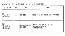
- “display number” and “display data / display position” can be specified in the first and second fields. Note that the third to fifth fields are not used (a NULL value).
- “execution processing type”, “argument number”, and “argument information” can be specified in the first to third fields. Note that the fourth and fifth fields are not used (is a NULL value).
- FIG. 12 is an explanatory diagram of an example of values that can be specified in the first to fifth fields of the scan command and an outline thereof. As shown in the figure, the first to fifth fields of the scan command are the same as the fields of the sub-display device command, and thus description thereof is omitted here.
- FIG. 13 is an explanatory diagram of an example of values that can be specified in the first and second fields of the display command and an outline thereof.
- the first field (display number) of the display command is a field for designating the number of data to be displayed on the display / light sensor unit 330 of the sub display device with sensor 230. That is, it indicates the number of sets designated in the second field (display data / display position).
- the second field (display data / display position) of the display command is a field indicating a set of image data itself to be displayed on the display / light sensor unit 330 of the sub-display device with sensor 230 and the display position (coordinates) of the data. It is. When a plurality of image data are displayed, a plurality of sets are designated in the second field.
- FIG. 14 is an explanatory diagram of an example of values that can be specified in the first to third fields of the processing command and an outline thereof.
- the first field (execution processing type) of the processing command is a field for designating identification information of processing (various applications, middleware, OS, etc.) to be executed by the main control unit that is the processing command transmission destination.
- the identification information may be any value as long as the process can be identified.
- the second field (argument number) of the processing command is a field for designating the number of various information (arguments) used during or after the process indicated by the identification information specified in the first field. That is, it indicates the number of data specified in the third field (argument information).
- the third field (argument information) of the processing command is a field for designating various information (arguments) used during or after the processing indicated by the identification information specified in the first field.
- the information used at the time of activation includes, for example, a parameter for designating an operation mode of a predetermined process designated in the first field, a display area, and the like.
- the information used after activation includes, for example, image data that is a target of character recognition by the character recognition application when a character recognition application is designated in the first field. Further, when a file transfer application is specified in the first field, a file to be transferred by the file transfer application can be cited.
- the image data shown in FIG. 15A is image data obtained as a result of scanning the entire sensor-equipped liquid crystal panel 301 when the object is not placed on the sensor-equipped liquid crystal panel 301.
- the image data shown in FIG. 15B is image data obtained as a result of scanning the entire sensor-equipped liquid crystal panel 301 when the user touches the sensor-equipped liquid crystal panel 301 with a finger.
- the amount of light received by the photosensor circuit 32 in the vicinity of the touch changes, so that the voltage output from the photosensor circuit 32 changes, and as a result, In the image data generated by the sensor control unit 602, the brightness of the pixel value of the portion touched by the user changes.
- the brightness of the pixel value corresponding to the user's finger is higher than that in the image data shown in (a) of FIG. 15.
- the smallest rectangular area (area PP) that includes all pixel values whose lightness changes more than a predetermined threshold value is “partial image data”.
- the image data indicated by the area AP is “whole image data”.
- the coordinate data in the entire image data (area AP) of the representative coordinates Z of the partial image data (area PP) is (Xa, Ya), and the coordinate data in the partial image data (area PP) is (Xp, Yp). It is.
- FIG. 16 is a block diagram showing the main part of the display / light sensor unit 330, particularly the configuration of the sensor built-in liquid crystal panel 301 and the configuration of the peripheral circuit 309.
- the sensor built-in liquid crystal panel 301 includes a pixel circuit 31 for setting light transmittance (brightness), and an optical sensor circuit 32 that outputs a voltage corresponding to the intensity of light received by itself.
- the pixel circuit 31 is used as a general term for the R pixel circuit 31r, the G pixel circuit 31g, and the B pixel circuit 31b corresponding to the red, green, and blue color filters, respectively.
- the m pixel circuits 31 are arranged in the column direction (vertical direction) and 3n in the row direction (horizontal direction) on the sensor built-in liquid crystal panel 301.
- a set of the R pixel circuit 31r, the G pixel circuit 31g, and the B pixel circuit 31b is continuously arranged in the row direction (lateral direction). This set forms one pixel.
- the high level voltage (TFT 33 is turned on) to the scanning signal line Gi connected to the gate terminal of the TFT (Thin FilmTransistor) 33 included in the pixel circuit 31. Voltage). Thereafter, a predetermined voltage is applied to the data signal line SRj connected to the source terminal of the TFT 33 of the R pixel circuit 31r.
- the light transmittance is also set for the G pixel circuit 31g and the B pixel circuit 31b. Then, by setting these light transmittances, an image is displayed on the sensor built-in liquid crystal panel 301.
- the optical sensor circuit 32 is arranged for each pixel.
- One pixel may be arranged in the vicinity of each of the R pixel circuit 31r, the G pixel circuit 31g, and the B pixel circuit 31b.
- the optical sensor circuit 32 In order for the optical sensor circuit 32 to output a voltage according to the light intensity, first, the sensor readout line RWi connected to one electrode of the capacitor 35 and the anode terminal of the photodiode 6 are connected. A predetermined voltage is applied to the sensor reset line RSi. In this state, when light is incident on the photodiode 6, a current corresponding to the amount of incident light flows through the photodiode 6. And according to the said electric current, the voltage of the connection point (henceforth connection node V) of the other electrode of the capacitor
- the power supply voltage VDD When the power supply voltage VDD is applied to the voltage application line SDj connected to the drain terminal of the sensor preamplifier 37, the voltage at the connection node V is amplified and output from the source terminal of the sensor preamplifier 37 to the sensing data output line SPj. Based on the output voltage, the amount of light received by the optical sensor circuit 32 can be calculated.
- liquid crystal panel drive circuit 304 the optical sensor drive circuit 305, and the sensor output amplifier 44, which are peripheral circuits of the sensor built-in liquid crystal panel 301, will be described.
- the liquid crystal panel driving circuit 304 is a circuit for driving the pixel circuit 31, and includes a scanning signal line driving circuit 3041 and a data signal line driving circuit 3042.
- the scanning signal line drive circuit 3041 sequentially selects one scanning signal line from the scanning signal lines G1 to Gm for each line time based on the timing control signal TC1 received from the liquid crystal panel control unit 601. A high level voltage is applied to the selected scanning signal line, and a low level voltage is applied to the other scanning signal lines.
- the data signal line driver circuit 3042 Based on the display data D (DR, DG, and DB) received from the liquid crystal panel controller 601, the data signal line driver circuit 3042 applies a predetermined voltage corresponding to the display data for one row for each line time. Are applied to the data signal lines SR1 to SRn, SG1 to SGn, and SB1 to SBn (line sequential method). Note that the data signal line driver circuit 3042 may be driven by a dot sequential method.
- the optical sensor driving circuit 305 is a circuit for driving the optical sensor circuit 32. Based on the timing control signal TC2 received from the sensor control unit 602, the optical sensor driving circuit 305 applies a predetermined sensor read signal line to each sensor read signal line selected from the sensor read signal lines RW1 to RWm for each line time. A read voltage is applied, and a voltage other than a predetermined read voltage is applied to the other sensor read signal lines. Similarly, based on the timing control signal TC2, a predetermined reset voltage is applied to the sensor reset signal line selected from the sensor reset signal lines RS1 to RSm for each line time, and the others. A voltage other than a predetermined reset voltage is applied to the sensor reset signal line.
- the sensing data output signal lines SP1 to SPn are grouped into p groups (p is an integer of 1 to n), and the sensing data output signal lines belonging to each group are connected via a switch 47 that is sequentially turned on in time division. And connected to the sensor output amplifier 44.
- the sensor output amplifier 44 amplifies the voltage from the group of sensing data output signal lines connected by the switch 47 and outputs the amplified voltage to the signal conversion circuit 306 as sensor output signals SS (SS1 to SSp).
- FIG. 1 is a block diagram showing a more detailed configuration of the main display device 210 and the sensor-equipped sub display device 230.
- the storage unit 911 of the main display device 210 includes a main-side BIOS program (first process) P11, a main-side boot loader B11, and a set of a plurality of main-side secondary boot loaders and main-side OS programs (second process, Candidate processing) is stored.
- a set of the main side secondary boot loader and the main side OS program in FIG. 1, the main side secondary boot loader B21 and the main side OS program P21, the main side secondary boot loader B22 and the main side OS program P22, main Three sets of the secondary boot loader B23 and the main OS program P23 are stored.
- the main-side secondary boot loader and the main-side OS program are not necessarily separate programs, and the main-side secondary boot loader and the main-side OS program may be combined into one program.
- the main-side BIOS program P11 is stored in, for example, the flash memory 16, and the set of the main-side boot loader B11 and a plurality of main-side secondary boot loaders and main-side OS programs is stored in the hard disk 17, for example. It is assumed that Each set of the main side secondary boot loader and the main side OS program is assumed to be divided and stored in predetermined partitions (areas) PA1 to PA3 as shown in the figure. Normally, at least one of the partitions is set to active (a start flag is set).
- the main BIOS program P11 is a BIOS (Basic Input Input Output System) program of the main display device 210.
- BIOS Basic Input Input Output System
- the main-side BIOS program P11 is assumed to be a generally known BIOS program, and is executed by the main-side main control unit 810 immediately after power is supplied to the main display device 210. Since the process performed by the main-side BIOS program P11 is the same as the process performed by a generally known BIOS program, detailed description thereof is omitted here.
- initialization processing POST: Power On Self Test
- POST code execution status information
- POST code execution status information
- the POST code holding unit 18 is a circuit or the like that can hold the value of the POST code and can reference the held value from the outside.
- the POST code holding unit 18 is provided on a mother board or the like.
- the main side boot loader B11 is a program called by the main side BIOS program P11.
- the main-side boot loader B11 has a function provided by a generally known boot loader, and is stored in the first sector (boot sector) such as a disk in which the main-side OS programs P21 to P23 are stored. ing.
- the sector is generally a sector called a master boot record (MBR).
- the main boot loader B11 is read and executed by the main main controller 810.
- the main side boot loader B11 determines a partition to be referred to, and executes the main side secondary boot loader stored in the head sector of the determined partition. Normally, a partition that is set to be active is a partition to be referred to.
- the first sector of each partition is generally a sector called a volume boot record (VBR) or a partition boot record (PBR).
- main secondary boot loaders B21, B22, and B23 are read and executed by the main main controller 810 as a result of the execution of the main boot loader B11. It is a program for starting.
- the main-side secondary boot loaders B21, B22, and B23 are assumed to be generally known secondary boot loaders, and are stored in the first sector of each partition such as a disk in which the main-side OS is stored. ing. Specific examples of the main secondary boot loaders B21, B22, and B23 include LILO (LInux LOader), GRUB (GRand Unified Bootloader), Windows Boot Manager, and NTLDR (NT Loader).
- the main OS program stored in the partition where the main secondary boot loader is stored is read into the main main control unit 810, It is activated.
- the main-side OS programs P21, P22, and P23 are programs of the OS of the main display device 210 (hereinafter, main-side OS).
- main-side OS the main side OS boot program is started by the main side secondary boot loader.
- the type of the main OS is not limited.
- the main OS programs P21, P22, and P23 are a Windows (registered trademark) XP program, a Windows Vista (registered trademark) program, a recovery program for restoring the OS, and the like.
- identification information of the corresponding main OS is added to the main OS programs P21, P22, and P23 so that they can be referred to from the outside.
- the main side main control unit 810 includes a main side boot loader execution unit 13 (execution control means), a main side secondary boot loader execution unit 14, and a main side OS activation unit 15.
- main side boot loader execution unit 13 execution control means
- main side secondary boot loader execution unit 14 main side OS startup unit 15
- main side OS startup unit 15 main side OS startup unit 15
- the main side boot loader execution unit 13 operates as a result of the main side boot loader B11 being read by the main side main control unit 810.
- the main-side boot loader execution unit 13 includes at least a timeout detection unit 131 and a secondary boot loader activation unit 132. Further, when a list of identification information (candidate processing information) of the main OS that can be booted by the main display device 210 is requested from the sub display device with sensor 230, the main boot loader execution unit 13 further It is configured to include a side OS list transmission unit 133 (specifically, the main side boot loader execution unit 13 is described in the main side boot loader B11 so as to include the main side OS list transmission unit 133). In the following, a list of identification information of main OSs that can be activated by the main display device 210 is referred to as a “main OS list”.
- the time-out detection unit 131 detects that a predetermined time has elapsed since the main-side boot loader B11 is read into the main-side main control unit 810.
- the secondary boot loader activation unit 132 normally operates as a trigger when the timeout detection unit 131 detects that the predetermined time has elapsed, and determines the partition set to be active as the partition to be referred to. To do. Then, the main secondary boot loader (any of B11 to B13) stored in the determined partition is read into the main main control unit 810.
- the main-side boot loader execution unit 13 is activated from the main-side activation OS designation unit 25 (described later) of the sensor-equipped sub-display device 230 via the communication control unit 913.
- the secondary boot loader activation unit 132 operates in response to the reception and stores the main OS corresponding to the specified identification information.
- the partition that is being used is determined as the partition to be referenced.
- the main-side boot loader execution unit 13 receives a processing command in which a request for the main-side OS list is specified via the communication control unit 913
- the main-side OS list transmission unit 133 responds to the reception.
- the main-side OS identification information acquired from the storage unit 911 is transmitted to the processing command request source as a main-side OS list.
- the timeout detection unit 131 further detects that a predetermined time has elapsed since the main OS list transmission unit 133 transmits the main OS list to the request source of the received processing command. Then, when the predetermined time has passed without specifying the main OS to be started, the secondary boot loader starting unit 132 stores the main secondary boot loaders (B11 to B11) stored in the partition set to active. (B13) is read into the main main control unit 810.
- the main-side secondary boot loader execution unit 14 executes as a result that one of the main-side secondary boot loaders B11 to B13 is read into the main-side main control unit 810 and executed by the secondary boot loader starting unit 132. It works. Then, the main OS is started by reading the main OS program stored in the same partition as the main secondary boot loader read into the main main controller 810 into the main main controller 810.
- the main-side OS activation unit 15 operates as a result of the main-side secondary boot loader execution unit 14 reading and executing any of the main-side OS programs P21, P22, and P23 into the main-side main control unit 810.
- the main OS is started.
- the storage unit 931 stores a sub-side BIOS program P31, a sub-side boot loader B31, and a set of the sub-side secondary boot loader B41 and the sub-side OS program P41.
- the sub-side secondary boot loader B41 and the sub-side OS program P41 are not necessarily separate programs, and the sub-side secondary boot loader B41 and the sub-side OS program P41 may be combined into one program. .
- the sub-side BIOS program P31 is stored in, for example, the flash memory 26, and the set of the sub-side boot loader B31 and the sub-side secondary boot loader B41 and the sub-side OS program P41 is stored in, for example, the hard disk 27. Assuming that Further, it is assumed that a set of the sub-side secondary boot loader B41 and the sub-side OS program P41 is stored in a predetermined partition PA4.
- the sub-side BIOS program P31 is a program of the BIOS of the sub-display device with sensor 230 (hereinafter referred to as sub-side BIOS).
- the sub-side BIOS program P31 is assumed to be a generally known BIOS program, and is executed by the sub-side main control unit 830 immediately after power is supplied to the sensor-equipped sub display device 230. Since the processing performed by the sub-side BIOS program P31 is the same as the processing performed by the generally known BIOS program, detailed description thereof is omitted here.
- the sub-side boot loader B31 is a program called by the sub-side BIOS program P31.
- the sub-side boot loader B31 has a function of a generally known boot loader, and is stored in the first sector (boot sector) such as a disk in which the sub-side OS program P41 is stored. .
- the sub-side boot loader B31 is read and executed by the sub-side main control unit 830. Then, the sub-side boot loader B31 executes the sub-side secondary boot loader B41 stored in the first sector of the partition.
- the sub-side secondary boot loader B41 is read and executed by the sub-side main control unit 830 as a result of the execution of the sub-side boot loader B31, and starts the sub-side OS program. It is a program.
- the sub-side secondary boot loader B41 is assumed to be a generally known secondary boot loader, and is stored in the top sector of each partition such as a disk in which the sub-side OS is stored.
- the sub-side secondary boot loader B41 is LILO, GRUB, WindowsWBoot Manager, NTLDR, or the like.
- the sub-side OS program P41 stored in the partition in which the sub-side secondary boot loader is stored is read into the sub-side main control unit 830. It is activated.
- sub-side OS program P41 is a program for the OS of the sensor-equipped sub-display device 230 (hereinafter, sub-side OS).
- the main display device 210 and the sensor-equipped sub-display device 230 are turned on simultaneously, it is possible to specify the OS activation of the main display device 210 from the sensor-equipped sub-display device 230. Therefore, the time required for starting the sub-side OS in the sub display device with sensor 230 is shorter than the time required for starting the main side OS in the main display device 210 as much as possible. Is preferable. Therefore, an OS that requires a relatively short time for the startup process, such as Linux or Tron, is suitable for the sub-side OS.
- the sub display device with sensor 230 When the sub display device with sensor 230 is attached to the main display device 210 (that is, when the wired communication unit 914 of the main display device 210 and the wired communication unit 934 of the sub display device with sensor 230 are connected). As described above, by turning on the power supply 917 of the main display device 210, power is supplied to the sub display device with sensor 230, and as a result, power is supplied to each part of the sub display device with sensor 230.
- the sub-side main control unit 830 includes a sub-side boot loader execution unit 21, a sub-side secondary boot loader execution unit 22, a sub-side OS activation unit 23, a POST code inspection unit (execution status determination unit) 24, And a main-side boot OS designation unit (execution designation means) 25.
- the POST code checking unit 24 and the main-side startup OS designation unit 25 operate after the sub-side OS is started up.
- the sub-side secondary boot loader B41 and the sub-side OS program P41 are combined into one program, the sub-side secondary boot loader execution unit 22 and the sub-side OS startup unit 23 are merged into one. May be.
- the sub-side boot loader execution unit 21 operates as a result of the sub-side boot loader B31 being read by the sub-side main control unit 830.
- the sub-side boot loader execution unit 21 reads the sub-side secondary boot loader B41 stored in the partition into the sub-side main control unit 830.
- the sub-side secondary boot loader execution unit 22 operates as a result of the sub-side secondary boot loader B 41 being read by the sub-side main load control unit 830 and executed by the sub-side boot loader execution unit 21. . Then, it starts by reading the sub-side OS program P41 into the sub-side main control unit 830.
- the sub-side OS startup unit 23 operates as a result of the sub-side OS program P41 being read by the sub-side secondary boot loader execution unit 22 and executed by the sub-side main control unit 830. Start the OS.
- the POST code checking unit 24 checks the POST code output from the main BIOS program P11 of the main display device 210 immediately after the sub OS is started.
- the POST code inspection unit 24 refers to the POST code output to the POST code holding unit 18 of the main display device 210 via the communication control unit 933.
- the progress status of the POST process performed by the main-side BIOS program P11 of the main display device 210 is checked, and (A) whether the POST process has been normally completed to the end, and (B ) It is determined whether the POST process is interrupted.
- the POST code inspection unit 24 determines that the POST process has been normally completed to the end. Then, the main side startup OS designation unit 25 is notified to that effect.
- the POST code checking unit 24 refers to the POST code output to the POST code holding unit 18. repeat. Note that the number of repeated references and the reference interval may be determined in advance or may be determined by a predetermined calculation.
- the POST code inspection unit 24 displays a predetermined message corresponding to the last referenced POST code on the display / light sensor unit 330 to notify the user that the POST process has been interrupted.
- the POST code inspection unit 24 generates display data including the predetermined message, and transmits the generated display data to the data processing unit 730, thereby causing the display / light sensor unit 330 to display the predetermined message. .
- the main-side startup OS designating unit 25 instructs the main display device 210 to start the main-side OS to be started, and the main-side startup OS designation unit 25 starts up the main display device 210.
- the OS identification information is transmitted to the main display device 210 via the communication control unit 933.
- the main boot OS designation unit 25 designates information for identifying the secondary boot loader activation unit 132 in the first field, designates “1” in the second field, and designates in the third field. Then, the processing command specifying the identification information of the main-side OS to be activated on the main display device 210 is transmitted to the main display device 210.
- the identification information of the main OS may be stored in the storage unit 931 in advance, or the main display device 210 may be inquired.
- the main-side startup OS designation unit 25 is further configured to include a main-side OS list request unit (candidate processing information acquisition unit) 251.
- the main OS list request unit 251 requests the main OS list from the main OS list transmission unit 133 of the main display device 210 via the communication control unit 933. Then, the main OS list transmitted from the main OS list transmitter 133 is received as a response to the request.
- the main-side OS list request unit 251 designates information for identifying the main-side OS list transmission unit 133 in the first field, and designates “1” in the second field. Then, a processing command in which the identification information of the main OS list request unit 251 is specified as a return source of the main OS list in the third field is transmitted to the main display device 210.
- the main-side OS that the main-side startup OS designation unit 25 causes the main display device 210 to boot may be calculated and specified based on a predetermined rule, or may be specified by being selected by the user.
- designated part 25 is further comprised so that the user presentation process part (candidate process selection means) 252 may be included.
- the user presentation processing unit 252 receives the main OS list stored in the storage unit 931 in advance or the main OS list request unit 251 receives the main OS list, the user presentation processing unit 252
- the sensor / built-in liquid crystal panel 301 of the display / light sensor unit 330 is displayed in a selectable manner by the user, and the main OS selected by the user is specified.
- the user presentation processing unit 252 generates display data including the main-side OS list, and transmits the generated display data to the data processing unit 730, whereby the display / light sensor unit 330 receives the main data.
- the side OS list is displayed.
- the user presentation processing unit 252 specifies “event” or “all” in the “data acquisition timing” field and acquires “coordinate data” indicating the position touched by the user, and the “data type” field.
- the sub display device command designating “coordinate” is transmitted to the data processing unit 730. If both coordinate data and partial image data (including coordinate data in a partial image) are desired, both “coordinate” and “partial image” are specified in the “data type” field.
- the optical sensor circuit 32 of the sensor built-in liquid crystal panel 301 detects at least one of a shadow image and a reflected image of a finger or a pen touched by the user.
- the image data received by the data processing unit 730 from the sensor control unit 602 changes.
- the data processing unit 730 transmits the coordinate data to the user presentation processing unit 252 as a response to the command within the sub display device, so that the user presentation processing unit 252 indicates the coordinate data received from the data processing unit 730.
- the main OS selected by the user can be specified based on the location where the identification information of the main OS is displayed.
- the main side startup OS specification unit 25 displays the main display.
- the main display OS 210 is instructed to be activated.
- the predetermined main OS may be determined in advance or may be determined by a predetermined calculation.
- FIG. 17 is a flowchart illustrating an example of a processing flow until the OS is started on the main display device.
- the sub display device with sensor 230 inquires of the main display device 210 about the identification information of the main side OS and causes the user to select the main side OS at the sub display device with sensor 230. .
- main display device 210 when the power of main display device 210 is turned on (YES in S11), power is supplied from wired communication unit 914 of main display device 210 to wired communication unit 934 of sub-display device with sensor 230 (S12). . Then, the main BIOS program P11 is executed (S13). As a result, the POST code is output to the POST code holding unit 18.
- the main-side boot loader B11 is read into the main-side main control unit 810 and executed (S14).
- step S12 power is supplied to each unit of the sensor-equipped sub display device 230 (YES in S15).
- the sub BIOS program P31 is executed (S16).
- the sub-side boot loader B31 is read into the sub-side main control unit 830 and executed (S17).
- the sub-side secondary boot loader B41 is read into the sub-side main control unit 830, and the sub-side OS program P41 is executed (S18).
- the sub-side OS is activated.
- the POST code checking unit 24 refers to the POST code output to the POST code holding unit 18 of the main display device 210, (A) whether the POST process has been normally completed, and (B) POST. It is determined whether the process is interrupted (S19). When it is determined that the POST process has not been completed normally until the end (POST process is interrupted) (NO in S20), POST code checking unit 24 displays / displays a predetermined message corresponding to the referred POST code. It is displayed on the optical sensor unit 330 (S21).
- the main-side OS list request unit 251 requests the main-side OS list from the main display device 210 (S22).
- the main-side boot loader execution unit 13 When the main-side boot loader execution unit 13 receives the request (YES in S23), the main-side OS list transmission unit 133 transmits the main-side OS list to the main-side OS list request unit 251 (S24). On the other hand, the main-side boot loader execution unit 13 does not receive the above request (NO in S23), and a time-out is detected that a predetermined time has elapsed since the main-side boot loader B11 was read into the main-side main control unit 810.
- the secondary boot loader starting unit 132 sets the main side secondary boot loader (any one of B11 to B13) stored in the active partition to the main side.
- the main-side secondary boot loader reads the main-side OS program stored in the same partition and loads the main-side OS program into the main-side main control unit 810 to start the main-side OS (S26). ).
- the user presentation processing unit 252 displays the received main-side OS list and the sensor built-in liquid crystal of the optical sensor unit 330. It is displayed on the panel 301 (S27).
- the main-side startup OS specifying unit 25 When the user selects one of the main-side OSs displayed on the sensor built-in liquid crystal panel 301 by touching with a finger, a pen, or the like (YES in S28), the main-side startup OS specifying unit 25 performs the above operation. In order to instruct activation of the selected main-side OS, the identification information of the selected main-side OS is transmitted to the main display device 210 (S29).
- the main-side startup OS designation unit 25 identifies the predetermined main-side OS in order to instruct the startup of the predetermined main-side OS. Information is transmitted to the main display device 210 (S31).
- the secondary boot loader activation unit 132 operates in response to the reception, and determines a partition in which the main-side OS corresponding to the received identification information is stored as a partition to be referred to. Then, the main side secondary boot loader (any of B11 to B13) stored in the determined partition is read into the main side main control unit 810 to execute the main side secondary boot loader, and the main side OS Is activated (S33).
- the main-side boot loader execution unit 13 does not receive the identification information of the main-side OS to be booted from the main-side boot OS designation unit 25 (NO in S32), and the timeout detection unit 131 displays the main-side OS list.
- the transmission unit 133 detects that a predetermined time has elapsed since the transmission of the main OS list to the main OS list request unit 251 (YES in S34)
- the secondary boot loader activation unit 132 is set to active.
- the main secondary boot loader (any of B11 to B13) stored in the partition being read is read into the main main control unit 810, and the read main secondary boot loader is stored in the same partition.
- the main OS is started by reading the main OS program into the main main controller 810 S35).
- the execution status of the BIOS of the main display device 210 is inspected by the sub display device with sensor 230, and the OS to be started up by the main display device 210 is designated from the sub display device with sensor 230.
- the present invention is applicable to other cases.
- each of a plurality of users owns a sensor-equipped sub-display device 230 stored in a state where the environment settings of the main-side OS are uniquely customized, and each user owns a sensor-equipped sub-display device 230
- a case where the main display device 210 is attached to the main display device 210 is used.
- the environment setting may be designated for the OS to be activated from the sub display device with sensor 230.
- each of the plurality of users owns the sensor-equipped sub display device 230 in which the login password of the main-side OS is set, and each user owns the sensor-equipped sub display device 230.
- a case where the display device 210 is used while being mounted is conceivable.
- the login password may be specified from the sensor-equipped sub display device 230.
- the sub display device with sensor 230 may be configured integrally with the main display device 210. .
- the configuration including the data processing unit 730 and the display / light sensor circuit control unit 630 has been described as the configuration of the sensor-equipped sub-display device 230.
- the configuration is not limited to this configuration.
- the sub-side main control unit 830 may directly control the display / light sensor circuit control unit 630, and the sub-side main control unit 830 may generate whole image data / partial image data / coordinate data.
- the sub-side main control unit 830 may directly control the display / light sensor unit 330.
- BIOS program is described as an example of the first process, but the present invention is not limited to this, and may be, for example, an environment acquisition program that acquires a temperature or the like.
- the processing control unit generates the execution status information indicating the execution status while executing the first processing, and executes the second processing after the first processing.
- a process control unit that is communicable with the execution unit and operable independently of the process execution unit, and obtains the generated execution status information from the process execution unit, and the acquired execution status
- Execution status determining means for determining whether or not the information is a predetermined value, and when the execution status determining means determines that the acquired execution status information is the predetermined value, the process execution unit can execute the information.
- Execution designation means for designating the process execution unit to execute any one of a plurality of candidate processes as the second process.
- control method of the processing control unit is a process for generating execution status information indicating the execution status while executing the first processing, and executing the second processing after the first processing.
- a method for controlling a processing control unit that is communicable with an execution unit and operable independently of the process execution unit, wherein the generated execution status information is acquired from the process execution unit and the acquisition is performed.
- the execution state determining step for determining whether or not the executed execution state information is a predetermined value; and when the acquired execution state information is determined to be the predetermined value in the execution state determination step, the processing execution unit An execution designation step that designates the process execution unit so that any one of a plurality of candidate processes that can be executed in the process is executed as the second process. And Nde.
- the process control unit can specify the second process to be executed by the process execution unit when the execution status of the first process being executed by the process execution unit is a predetermined condition.
- the process control unit can control the subsequent process (second process) executed by the process execution unit according to the execution status of the preceding process (first process) in the process execution unit.
- the process control unit is the above-described configuration, wherein the execution designation unit further acquires candidate process information indicating each of the plurality of candidate processes from the process execution unit.
- the execution specifying means may be configured to transmit information specifying any one of the acquired candidate process information to the process execution unit.
- candidate process information indicating each of the plurality of candidate processes can be acquired from the process execution unit. Then, any one of the candidate processes indicated by the acquired candidate process information can be transmitted to the process execution unit.
- the process control unit can designate the second process to be executed by the process execution unit by transmitting any one of the candidate process information acquired from the process execution unit to the process execution unit.
- the process control unit can designate the second process without knowing in advance the candidate process that can be designated as the second process.
- the processing control unit is configured so that, in the above configuration, the execution specifying unit further presents the candidate processing information acquired by the candidate processing information acquiring unit to the user, It is good also as a structure provided with the candidate process selection means which makes a user select any one, and the said execution designation
- the candidate process information can be presented to the user and the user can select any one of the presented candidate process information. Then, the selected candidate process information can be transmitted to the process execution unit.
- the user can cause the process execution unit to execute the candidate process selected by the user.
- the process control unit is configured so that, in the above configuration, the execution designation unit is configured to execute the predetermined candidate process when the candidate process information presented by the candidate process selection unit is not selected within a predetermined time. Information specifying the information may be transmitted to the processing execution unit.
- the predetermined candidate process information can be transmitted to the process execution unit.
- the process execution unit can execute the second process.
- the process control unit has the above-described configuration, wherein the process execution unit executes any one of a plurality of operating systems executable by the own unit after executing the BIOS as the first process.
- the execution process may be executed as the second process, and the execution specifying unit may specify any one of the operating systems as the second process.
- the process execution unit further executes the operating system as the second process after executing the BIOS as the first process, and the process control unit performs the operation system as the second process. Can be specified.
- the execution status information is specifically a POST (Power (On Self Test) code output by executing the BIOS, and the value indicates the normal end of the POST process.
- the process control unit designates an operating system to be activated by the process execution unit.
- the process execution unit generates execution status information indicating the execution status while executing the first process, and a plurality of candidates that can be executed by the own unit after the first process.
- a process execution unit that executes any one of the processes as a second process and is communicable with the process control unit, and receives an instruction to execute the second process from the process control unit that can read the execution status information.
- an execution control means for executing the designated second process after the first process.
- the method for controlling a process execution unit generates execution status information indicating the execution status while executing the first process, and can be executed by the own unit after the first process.
- the process execution unit can execute the second process in response to an instruction from the process control unit when the execution status of the first process reaches a predetermined status.
- the process execution unit can execute the subsequent process (second process) designated by the process control unit in accordance with the execution status of the preceding process (first process).
- the process execution unit according to the present invention is configured so that, when the process control unit does not designate the second process within a predetermined time after the execution of the first process, the execution control means It is good also as a structure which performs the said 2nd process.
- the predetermined second process can be executed.
- the process execution unit can execute the second process even if the second process is not designated.
- the information processing apparatus is characterized in that the process control unit and the process execution unit are connected by wire.
- the information processing apparatus has the same effects as the process control unit and the process execution unit.
- the process control unit and the process execution unit may be realized by a computer.
- the process control unit and the process execution unit are realized by a computer by operating the computer as each of the means.
- the control program for the display device and the computer-readable recording medium on which the control program is recorded also fall within the scope of the present invention.
- each block of the main display device 210 and the sensor-equipped sub display device 230 in particular, the main side main control unit 810, the sub side main control unit 830, the data processing unit 730, and the display / light sensor circuit control unit 630, It may be configured by wear logic, or may be realized by software using a CPU as follows.
- the main display device 210 and the sensor-equipped sub-display device 230 develop a CPU (central processing unit) that executes instructions of a control program that realizes each function, a ROM (read memory only) that stores the program, and the program.
- the object of the present invention is to read the program code (execution format program, intermediate code program, source program) of the control program of the main display device 210 and the sensor-equipped sub display device 230, which is software for realizing the above-described functions, by a computer. It is also achieved by supplying the recording medium recorded as possible to the main display device 210 and the sub-display device with sensor 230, and the computer (or CPU or MPU) reads out and executes the program code recorded on the recording medium. Is possible.
- Examples of the recording medium include tapes such as magnetic tapes and cassette tapes, magnetic disks such as floppy (registered trademark) disks / hard disks, and disks including optical disks such as CD-ROM / MO / MD / DVD / CD-R.
- Card system such as IC card, IC card (including memory card) / optical card, or semiconductor memory system such as mask ROM / EPROM / EEPROM / flash ROM.
- the main display device 210 and the sensor-equipped sub display device 230 may be configured to be connectable to a communication network, and the program code may be supplied via the communication network.
- the communication network is not particularly limited.
- the Internet intranet, extranet, LAN, ISDN, VAN, CATV communication network, virtual private network, telephone line network, mobile communication network, satellite communication. A net or the like is available.
- the transmission medium constituting the communication network is not particularly limited.
- infrared rays such as IrDA and remote control, Bluetooth ( (Registered trademark), IEEE802.11 radio, HDR, mobile phone network, satellite line, terrestrial digital network, and the like can also be used.
- the present invention can also be realized in the form of a computer data signal embedded in a carrier wave in which the program code is embodied by electronic transmission.
- the present invention can be applied to an information processing apparatus including a main device (main display device) and a sub device (sub display device with a sensor).
- a main device main display device
- a sub device sub display device with a sensor
- the present invention can be suitably applied to a notebook computer equipped with a main display and a sub display.
- Main side boot loader execution part (execution control means) 14 Main-side secondary boot loader execution unit 15 Main-side OS startup unit 18 POST code holding unit 21 Sub-side boot loader execution unit 22 Sub-side secondary boot loader execution unit 23 Sub-side OS startup unit 24 POST code checking unit (execution status) Judgment means) 25 Main side boot OS designation part (execution designation means) 133 Main-side OS list transmission unit 200 Two-screen display device (information processing device) 210 Main display device (processing execution unit) 230 Sub-display with sensor (processing control unit) 251 Main-side OS list request section (candidate processing information acquisition means) 252 User presentation processing unit (candidate process selection means) P11 Main BIOS program (first process) B21 to B23 Main side secondary boot loader (second process, candidate process) P21 to P23 Main OS program (second process, candidate process)
Landscapes
- Engineering & Computer Science (AREA)
- General Engineering & Computer Science (AREA)
- Theoretical Computer Science (AREA)
- Physics & Mathematics (AREA)
- General Physics & Mathematics (AREA)
- Human Computer Interaction (AREA)
- Computer Hardware Design (AREA)
- Quality & Reliability (AREA)
- Controls And Circuits For Display Device (AREA)
- Stored Programmes (AREA)
Abstract
メイン表示装置(210)とは独立して動作可能なセンサ付きサブ表示装置(230)は、メイン表示装置(210)がメイン側BIOSプログラム(P11)を実行しながら生成したPOSTコードを取得するとともに、当該取得したPOSTコードが所定値であるか否かを判定するPOSTコード検査部(24)と、POSTコードが上記所定値であると判定された場合、メイン表示装置(210)において実行可能な複数のメイン側OSプログラム(P21)から(P23)のいずれか1つを実行するように指定するメイン側起動OS指定部(25)とを備える。
Description
本発明は、外部装置にて実行される処理を制御する処理制御ユニット、処理実行ユニット、情報処理装置、制御方法、制御プログラム、および制御プログラムを記録したコンピュータ読み取り可能な記録媒体に関するものである。
近年、ノートPC(Personal Computer)に代表されるような、携帯型の情報処理装置が種々開発されており、広く普及している。このような情報処理装置では、その操作性の向上を図るために、様々な機能が設けられている。その一例として、メインディスプレイを含むメイン表示装置とは別に、サブディスプレイを含むサブ表示装置を設け、サブ表示装置にて、マウスポインティング操作、テンキー入力操作、メニュー画面表示などを可能とする機能がある。
このようなサブ表示装置を搭載したノートPCに関する従来技術が、特許文献1~4に開示されている。
特許文献1では、BIOS(Basic Input Output System)にパスワードが設定されている場合、BIOSは、まず、サブ表示装置およびそのコントローラを表示可能な状態とし、パスワードの入力要求を当該サブ表示装置に表示するように制御する技術が開示されている。
特許文献2では、メイン表示装置に表示されているマウスポインタの近くに表示エリアを確保し、当該表示エリアに、サブ表示装置で扱う切り替えメニュー画面を表示する技術が開示されている。
特許文献3では、主表示装置に表示される主操作画面を含むデスクトップ全体の画面イメージを、タッチ操作によりマウスポインタの位置を指示する操作画面として、サブ表示装置に表示する技術が開示されている。
特許文献4では、ノートPCが備える機能ボタンが操作されたとき、機能を選択するメニューをサブ表示装置に表示するとともに、ユーザがサブ表示装置を操作して、上記メニューからテンキーを選択すると、ユーザ操作可能なテンキーをサブ表示装置に表示する技術が開示されている。
しかしながら、従来のノートPCは、メイン表示装置に制御部(具体的には、CPU(central processing unit))が設けられ、サブ表示装置は当該制御部によって制御される構成となっている。
そのため、メイン表示装置の処理中に不具合が生じ、メイン表示装置の制御だけでなく、サブ表示装置の表示制御も不可能な状態にある場合、不具合の状況(ステータス)をユーザに提示することができないという問題がある。
また、メイン表示装置の動作状況に応じた処理を、サブ表示装置が実行することができないという問題がある。具体例を挙げれば、メイン表示装置の起動処理に不具合がある場合、サブ表示装置にてその旨を表示したり、上記起動処理に不具合が無い場合、メイン表示装置が起動するOS(Operating System)をサブ表示装置から指定するといった処理を行うことができない。
上記問題点を解決するために、メイン表示装置およびサブ表示装置のそれぞれが制御部を備える構成とし、サブ表示装置からメイン表示装置の動作状況を参照したり、メイン表示装置の動作状況に応じて、サブ表示装置からメイン表示装置を制御することが考えられる。このようなノートPCは、上述した特許文献1~4には開示されていない。
本発明は、上記の問題点に鑑みてなされたものであり、その目的は、メイン装置およびサブ装置を有する情報処理装置において、メイン装置での処理の実行状況に応じて、メイン装置が実行すべき処理を、サブ装置から制御することができる処理制御ユニット、処理実行ユニット、情報処理装置、制御方法、制御プログラム、および制御プログラムを記録したコンピュータ読み取り可能な記録媒体を提供することにある。
上記課題を解決するために、本発明に係る処理制御ユニットは、第1処理を実行しながら、その実行状況を示す実行状況情報を生成し、かつ、上記第1処理の後、第2処理を実行する処理実行ユニットと通信可能であり、上記処理実行ユニットとは独立して動作可能な処理制御ユニットであって、上記生成された上記実行状況情報を上記処理実行ユニットから取得するとともに、当該取得した実行状況情報が所定値であるか否かを判定する実行状況判定手段と、上記実行状況判定手段が、上記取得した実行状況情報が上記所定値であると判定した場合、上記処理実行ユニットにおいて実行可能な複数の候補処理のいずれか1つを上記第2処理として実行するように、上記処理実行ユニットに対して指定する実行指定手段とを備えることを特徴としている。
また、本発明に係る処理制御ユニットの制御方法は、第1処理を実行しながら、その実行状況を示す実行状況情報を生成し、かつ、上記第1処理の後、第2処理を実行する処理実行ユニットと通信可能であり、上記処理実行ユニットとは独立して動作可能な処理制御ユニットの制御方法であって、上記生成された上記実行状況情報を上記処理実行ユニットから取得するとともに、当該取得した実行状況情報が所定値であるか否かを判定する実行状況判定ステップと、上記実行状況判定ステップにて、上記取得した実行状況情報が上記所定値であると判定した場合、上記処理実行ユニットにおいて実行可能な複数の候補処理のいずれか1つを上記第2処理として実行するように、上記処理実行ユニットに対して指定する実行指定ステップとを含むことを特徴としている。
上記の構成によれば、上記実行状況情報を処理実行ユニットから取得し、当該取得した実行状況情報が所定値であるか否かを判定することができる。また、上記取得した実行状況情報が上記所定値であると判定した場合、上記複数の候補処理のいずれか1つを、処理実行ユニットにて第1処理の後に実行される第2処理として指定することができる。
よって、処理制御ユニットは、処理実行ユニットが実行している第1処理の実行状況が所定の状況である場合に、処理実行ユニットが実行可能な複数の候補処理のうちの1つを第2処理として指定することできる。
したがって、処理制御ユニットは、処理実行ユニットでの前段処理(第1処理)の実行状況に応じて、処理実行ユニットが実行する後段処理(第2処理)を制御することができるという効果を奏する。
なお、処理制御ユニットは、処理実行ユニットとは独立して動作可能であるので、処理実行ユニットでの前段処理(第1処理)の実行結果に依存することなく、処理制御ユニットから上記実行状況を確認することができる。そのため、処理実行ユニットでの前段処理(第1処理)中に何らかの不具合が生じた場合であっても、処理制御ユニットから処理実行ユニットでの処理の実行状況を確認することができる。
上記課題を解決するために、本発明に係る処理実行ユニットは、第1処理を実行しながら、その実行状況を示す実行状況情報を生成し、かつ、上記第1処理の後、自ユニットにて実行可能な複数の候補処理のいずれか1つを第2処理として実行する、処理制御ユニットと通信可能な処理実行ユニットであって、上記実行状況情報を読み出し可能な処理制御ユニットから上記第2処理の実行の指定を受け付けるとともに、上記第1処理の後、当該指定された上記第2処理を実行する実行制御手段とを備えることを特徴としている。
また、本発明に係る処理実行ユニットの制御方法は、第1処理を実行しながら、その実行状況を示す実行状況情報を生成し、かつ、上記第1処理の後、自ユニットにて実行可能な複数の候補処理のいずれか1つを第2処理として実行する、処理制御ユニットと通信可能な処理実行ユニットの制御方法であって、上記実行状況情報を読み出し可能な処理制御ユニットから上記第2処理の実行の指定を受け付けるとともに、上記第1処理の後、当該指定された上記第2処理を実行する実行制御ステップとを含むことを特徴としている。
上記の構成によれば、第1処理が実行され、所定の上記実行状況情報を生成した後、処理制御ユニットから指定された上記第2処理を実行することができる。
よって、処理実行ユニットは、第1処理の実行状況が所定の状況に達した場合、処理制御ユニットからの指示に応じて第2処理を実行することできる。
したがって、処理実行ユニットは、前段処理(第1処理)の実行状況に応じて、処理制御ユニットからの指定された後段処理(第2処理)を実行することができるという効果を奏する。
なお、処理制御ユニットは、処理実行ユニットとは独立して動作可能であるので、処理実行ユニットでの前段処理(第1処理)の実行結果に依存することなく、処理制御ユニットから上記実行状況を確認することができる。そのため、処理実行ユニットでの前段処理(第1処理)中に何らかの不具合が生じた場合であっても、処理制御ユニットから処理実行ユニットでの処理の実行状況を確認することができる。
本発明の他の目的、特徴、および優れた点は、以下に示す記載によって十分分かるであろう。また、本発明の利点は、添付図面を参照した次の説明で明白になるであろう。
本発明の一実施形態について図1から図17に基づいて説明すると以下の通りである。
(発明の概要)
本発明の概要は、メイン表示装置(処理実行ユニット)210で実行される第1処理の実行状況が所定の状況である場合に、メイン表示装置210にて実行可能な第2処理を、メイン表示装置とは独立して動作可能なセンサ付きサブ表示装置(処理制御ユニット)230から指定することである。本実施形態では、特に、メイン表示装置210の電源投入直後のBIOS(Basic Input Output System)の実行状況が所定の状況である場合に、メイン表示装置210にて実行可能なOS(Operating System)の起動処理を、センサ付きサブ表示装置230から指定するケースを例に挙げて説明する。なお、メイン表示装置210は、自装置で実行可能な複数のOSがインストールされており、そのうちのいずれか1つを起動するようになっている(マルチブートの状態である)ものとする。
本発明の概要は、メイン表示装置(処理実行ユニット)210で実行される第1処理の実行状況が所定の状況である場合に、メイン表示装置210にて実行可能な第2処理を、メイン表示装置とは独立して動作可能なセンサ付きサブ表示装置(処理制御ユニット)230から指定することである。本実施形態では、特に、メイン表示装置210の電源投入直後のBIOS(Basic Input Output System)の実行状況が所定の状況である場合に、メイン表示装置210にて実行可能なOS(Operating System)の起動処理を、センサ付きサブ表示装置230から指定するケースを例に挙げて説明する。なお、メイン表示装置210は、自装置で実行可能な複数のOSがインストールされており、そのうちのいずれか1つを起動するようになっている(マルチブートの状態である)ものとする。
まず、メイン表示装置210にセンサ付きサブ表示装置230を装着させた、2画面表示装置(情報処理装置)200の概要について説明し、その後、メイン表示装置210およびセンサ付きサブ表示装置230について説明する。
(2画面表示装置の概要)
2画面表示装置200は、データの表示が可能な液晶パネル311を備えるメイン表示装置210と、データの表示に加え、近傍の対象物の画像検出が可能なセンサ内蔵液晶パネル301(後述する)を備えるセンサ付きサブ表示装置230とを有する装置である。
2画面表示装置200は、データの表示が可能な液晶パネル311を備えるメイン表示装置210と、データの表示に加え、近傍の対象物の画像検出が可能なセンサ内蔵液晶パネル301(後述する)を備えるセンサ付きサブ表示装置230とを有する装置である。
メイン表示装置210とセンサ付きサブ表示装置230とは、着脱可能な構成となっている。そして、メイン表示装置210にセンサ付きサブ表示装置230が装着されている場合、相互に有線通信可能な状態となり、互いに相手側の装置に「装置間コマンド」を送信することによって、相手側の装置を制御可能な構成となっている。装置間コマンドの詳細については後述する。
なお、メイン表示装置210およびセンサ付きサブ表示装置230は、それぞれ、自装置を制御する制御部を備えている。そのため、メイン表示装置210とセンサ付きサブ表示装置230とを分離した状態では、それぞれ単体で動作可能である。
図2を参照しながら、2画面表示装置200の具体例について説明する。図2の(a)は、2画面表示装置200の具体例を示す模式図である。図示のように、本実施の形態では、2画面表示装置200として、従来のタッチパッドの代わりにセンサ付きサブ表示装置230を内部に備える、ノートPC(Personal Computer)を想定している。この場合、センサ付きサブ表示装置230以外の部分(表示部310やキーボード920を含む部分)が、メイン表示装置210に相当する。なお、図2の(a)に示した状態は、メイン表示装置210の内部にセンサ付きサブ表示装置230が装着されている状態である。メイン表示装置210のタッチパッドに相当する部分は透明であり、ユーザは、内部に装着されたセンサ付きサブ表示装置230のセンサ内蔵液晶パネル301を操作できるようになっている。
図2の(b)は、図2の(a)に示したノートPCにおいて、センサ付きサブ表示装置230をメイン表示装置210の内部から取り出して分離した状態を示す模式図である。上述したように、メイン表示装置210およびセンサ付きサブ表示装置230は、それぞれ単体でも動作可能であるので、この状態では、メイン表示装置210は、タッチパッド機能が無いノートPCとして動作することが可能である。また、センサ付きサブ表示装置230は、例えば、センサ内蔵液晶パネル301を備えるリモコンやPDA(Personal Digital Assistant)などとして動作することができる。
(センサ内蔵液晶パネルの概要)
上述したように、センサ付きサブ表示装置230が備えるセンサ内蔵液晶パネル301は、データの表示に加え、近傍の対象物の画像検出が可能な液晶パネルである。ここで、対象物の画像検出とは、例えば、ユーザが指やペンなどでポインティング(タッチ)した位置の検出や、印刷物等の画像の読み取り(スキャン)である。なお、表示に用いるデバイスは、液晶パネルに限定されるものではなく、有機EL(Electro Luminescence)パネルなどであってもよい。
上述したように、センサ付きサブ表示装置230が備えるセンサ内蔵液晶パネル301は、データの表示に加え、近傍の対象物の画像検出が可能な液晶パネルである。ここで、対象物の画像検出とは、例えば、ユーザが指やペンなどでポインティング(タッチ)した位置の検出や、印刷物等の画像の読み取り(スキャン)である。なお、表示に用いるデバイスは、液晶パネルに限定されるものではなく、有機EL(Electro Luminescence)パネルなどであってもよい。
図3を参照しながら、センサ内蔵液晶パネル301の構造について説明する。図3は、センサ内蔵液晶パネル301の断面を模式的に示す図である。なお、ここで説明するセンサ内蔵液晶パネル301は一例であり、表示面と読取面とが共用されているものであれば、任意の構造のものが利用できる。
図示のとおり、センサ内蔵液晶パネル301は、背面側に配置されるアクティブマトリクス基板51Aと、表面側に配置される対向基板51Bとを備え、これら基板の間に液晶層52を挟持した構造を有している。アクティブマトリクス基板51Aには、画素電極56、データ信号線57、光センサ回路32(図示せず)、配向膜58、偏光板59などが設けられる。対向基板51Bには、カラーフィルタ53r(赤)、53g(緑)、53b(青)、遮光膜54、対向電極55、配向膜58、偏光板59などが設けられる。また、センサ内蔵液晶パネル301の背面には、バックライト307が設けられている。
なお、光センサ回路32に含まれるフォトダイオード6は、青のカラーフィルタ53bを設けた画素電極56の近傍に設けられているが、この構成に限定されるものではない。赤のカラーフィルタ53rを設けた画素電極56の近傍に設けてもよいし、緑のカラーフィルタ53gを設けた画素電極56の近傍に設けてもよい。
次に、図4の(a)および図4の(b)を参照しながら、ユーザが、指やペンで、センサ内蔵液晶パネル301上をタッチした場合を例に挙げ、そのタッチした位置を検出する2種類の方法について説明する。
図4の(a)は、反射像を検知することにより、ユーザがタッチした位置を検出する様子を示す模式図である。バックライト307から光63が出射されると、フォトダイオード6を含む光センサ回路32は、指などの対象物64により反射された光63を検知する。これにより、対象物64の反射像を検知することができる。このように、センサ内蔵液晶パネル301は、反射像を検知することにより、タッチした位置を検出することができる。
また、図4の(b)は、影像を検知することにより、ユーザがタッチした位置を検出する様子を示す模式図である。図4の(b)に示すように、フォトダイオード6を含む光センサ回路32は、対向基板51Bなどを透過した外光61を検知する。しかしながら、ペンなどの対象物62がある場合は、外光61の入射が妨げられるので、光センサ回路32が検知する光量が減る。これにより、対象物62の影像を検知することができる。このように、センサ内蔵液晶パネル301は、影像を検知することにより、タッチした位置を検出することもできる。
上述のように、フォトダイオード6は、バックライト307より出射された光の反射光(影像)を検知してもよいし、外光による影像を検知してもよい。また、上記2種類の検知方法を併用して、影像と反射像とを両方を同時に検知するようにしてもよい。
(メイン表示装置およびセンサ付きサブ表示装置の要部構成)
次に、図5を参照しながら、メイン表示装置210およびセンサ付きサブ表示装置230の要部構成について説明する。図5は、メイン表示装置210およびセンサ付きサブ表示装置230の要部構成を示すブロック図である。
次に、図5を参照しながら、メイン表示装置210およびセンサ付きサブ表示装置230の要部構成について説明する。図5は、メイン表示装置210およびセンサ付きサブ表示装置230の要部構成を示すブロック図である。
(センサ付きサブ表示装置の要部構成)
まず、センサ付きサブ表示装置230の要部構成について説明する。図示のように、センサ付きサブ表示装置230は、表示/光センサ部330、表示/光センサ回路制御部630、データ処理部730、サブ側主制御部830、記憶部931、一次記憶部932、通信制御部933、有線通信部934、近距離無線通信部935、電界強度検出部936、バッテリー937、および電源切替部938を備えている。
まず、センサ付きサブ表示装置230の要部構成について説明する。図示のように、センサ付きサブ表示装置230は、表示/光センサ部330、表示/光センサ回路制御部630、データ処理部730、サブ側主制御部830、記憶部931、一次記憶部932、通信制御部933、有線通信部934、近距離無線通信部935、電界強度検出部936、バッテリー937、および電源切替部938を備えている。
表示/光センサ部330は、いわゆる光センサ内蔵液晶表示装置である。表示/光センサ部330は、センサ内蔵液晶パネル301、バックライト307、それらを駆動するための周辺回路309を含んで構成される。表示/光センサ部330の詳細な構成については後述する。
次に、表示/光センサ回路制御部630は、表示/光センサ部330の周辺回路309を制御するデバイスドライバとしての機能を備えるものである。表示/光センサ回路制御部630の詳細な構成については後述する。
次に、データ処理部730は、サブ側主制御部830から受信する「サブ表示装置内コマンド」に基づいて、表示/光センサ回路制御部630に指示を与えるミドルウェアとしての機能を備えるものである。データ処理部730の詳細な構成については後述する。また、サブ表示装置内コマンドの詳細についても後述する。
次に、サブ側主制御部830は、センサ付きサブ表示装置230が備える各部の動作を制御するものである。サブ側主制御部830は、記憶部931に記憶されている各種プログラムを読み出して、センサ付きサブ表示装置230の各部を制御し、センサ付きサブ表示装置230が備える各種機能を実現する。
サブ側主制御部830は、センサ内蔵液晶パネル301に表示データを表示させたり、センサ内蔵液晶パネル301にて対象物のスキャンを行なわせるために、データ処理部730に対して、サブ表示装置内コマンドおよび表示データを送信する。なお、サブ表示装置内コマンドに「データ種別」を指定した場合は、当該サブ表示装置内コマンドの応答として、全体画像データ、部分画像データ、および座標データの少なくともいずれか1つを、データ処理部730から受信する。
また、サブ側主制御部830は、メイン表示装置210からの制御を受け付ける。具体的には、メイン表示装置210のメイン側主制御部810が送信した装置間コマンドを受信し、当該受信した装置間コマンドの種類に応じて、下記(1)から(3)のいずれかに示す処理を実行する。
まず、(1)受信した装置間コマンドが、表示/光センサ部330の近傍に位置する対象物のスキャンを行なわせることを指定する「スキャンコマンド」(詳細は後述する)である場合、サブ側主制御部830は、当該受信したスキャンコマンドを、サブ表示装置内コマンドに変換するとともに、当該変換後のサブ表示装置内コマンドをデータ処理部730に送信する。なお、上記変換は、スキャンコマンドから「第0」フィールド(後述する)を取り除くことにより行なわれる。
なお、サブ側主制御部830は、上記変換後のサブ表示装置内コマンドの応答として、全体画像データ、部分画像データ、および座標データの少なくともいずれか1つをデータ処理部730から受信した場合、当該受信したデータを、メイン側主制御部810に送信する。
次に、(2)受信した装置間コマンドが、表示/光センサ部330に、写真やアイコンなどの画像データの表示を行なわせることを指定する「表示コマンド」(詳細は後述する)である場合、サブ側主制御部830は、当該表示コマンドに指定された情報に基づいて表示データを生成するとともに、当該生成した表示データをデータ処理部730に送信する。
次に、(3)受信した装置間コマンドが、所定処理を実行させることを指定する「処理コマンド」(詳細は後述する)である場合、サブ側主制御部830は、当該処理コマンドに指定された所定処理を実行する。
サブ側主制御部830が実行する上記所定処理とは、例えば、データ処理部730から得られた画像データに対する文字認識処理や画像処理、センサ付きサブ表示装置230の通信制御部933を用いた通信接続処理やファイル転送処理など、センサ付きサブ表示装置230が有する各種アプリケーションやミドルウェア等の実行処理である。
さらに、サブ側主制御部830は、メイン表示装置210に対して所定処理の実行を指示する。具体的には、処理コマンドとしての装置間コマンドを、メイン表示装置210のメイン側主制御部810に送信する。メイン側主制御部810が実行する上記所定処理とは、例えば、メイン表示装置210のOS(Operating System)の起動処理、メイン表示装置210の通信制御部913を用いた通信接続処理やファイル転送処理などの、メイン表示装置210が有する各種アプリケーションやミドルウェア等の実行処理である。
なお、表示/光センサ回路制御部630、データ処理部730、およびサブ側主制御部830は、それぞれ、CPU(Central Processing Unit)およびメモリ等で構成することができる。また、データ処理部730は、ASIC(application specific integrate circuit)などの回路で構成されていてもよい。
次に、記憶部931は、サブ側主制御部830が実行する(1)各部の制御プログラム、(2)OSプログラム、(3)アプリケーションプログラム、および、(4)これらプログラムを実行するときに読み出す各種データを記録するものである。記憶部931は、フラッシュメモリなどの不揮発性の記憶装置によって構成される。
一次記憶部932は、RAM(Random Access Memory)などの揮発性の記憶装置によって構成されるものであり、サブ側主制御部830が上述の各種プログラムを実行する過程でデータを一時的に保持するための作業領域として使用される。
次に、通信制御部933は、センサ付きサブ表示装置230が、メイン表示装置210と通信を行なうための有線通信部934、並びに、メイン表示装置210および図示しない外部装置のいずれかと通信を行なうための近距離無線通信部935を制御するものである。
すなわち、通信制御部933は、メイン表示装置210から、有線通信部934および近距離無線通信部935のいずれかを介して送信される装置間コマンドおよび各種データをサブ側主制御部830に送信する。また、通信制御部933は、サブ側主制御部830からの指示に応じて、サブ側主制御部830から送信される装置間コマンドおよび各種データを、有線通信部934および近距離無線通信部935のいずれかを介して、メイン表示装置210へ送信する。
また、通信制御部933は、近距離無線通信部935を介して、外部装置との間で各種データをやりとりする。
有線通信部934は、メイン表示装置210の有線通信部914と接続可能な構成となっている。本実施の形態では、有線通信部934と、メイン表示装置210の有線通信部914とは、USB(universal serial bus)接続されることを想定している。
そして、接続時には、有線通信部934は、通信線を用いて、メイン表示装置210の有線通信部914と相互に信号の送受信が可能であるとともに、電力線を用いて、メイン表示装置210の有線通信部914から電力の供給を受けることができる。そして、メイン表示装置210の有線通信部914から電力の供給を受けると、有線通信部934は、電源切替部938へ電力を供給する。
近距離無線通信部935は、メイン表示装置210の近距離無線通信部915との間、および、外部装置との間で形成される無線通信経路を用いて、相互に通信可能な構成となっている。本実施の形態では、上記無線通信経路に、Bluetooth(登録商標)(以下、単にBluetoothと表記する)通信を適用することを想定している。すなわち、近距離無線通信部935は、Bluetooth通信にて信号の送受信を行なうことのできる通信部である。なお、上記無線通信経路は、信号の送受信を行なえるものであればよく、IEEE802.11無線やZigBee(登録商標)等を適用してもよい。
次に、電界強度検出部936は、サブ側主制御部830からの指示に応じて、近距離無線通信部935が受信する信号の強度(RSSI(Received Signal Strength Indication):受信電界強度)を検出するものである。そして、当該検出の結果を、サブ側主制御部830に送信する。
次に、電源切替部938は、有線通信部934がメイン表示装置210の有線通信部914から電力の供給を受けている場合、センサ付きサブ表示装置230が備える各部に、メイン表示装置210から供給されている電力を供給する。一方、有線通信部934がメイン表示装置210の有線通信部914から電力の供給を受けていない場合、電源切替部938は、センサ付きサブ表示装置230が備える各部に、バッテリー937の電力を供給する。
(メイン表示装置の要部構成)
次に、メイン表示装置210の要部構成について説明する。図示のように、メイン表示装置210は、表示部310、表示回路制御部610、表示データ処理部710、メイン側主制御部810、記憶部911、一次記憶部912、通信制御部913、有線通信部914、近距離無線通信部915、有線/無線ネットワーク通信部916、電源917、操作部919、音声出力部924、および音声入力部925を備えている。
次に、メイン表示装置210の要部構成について説明する。図示のように、メイン表示装置210は、表示部310、表示回路制御部610、表示データ処理部710、メイン側主制御部810、記憶部911、一次記憶部912、通信制御部913、有線通信部914、近距離無線通信部915、有線/無線ネットワーク通信部916、電源917、操作部919、音声出力部924、および音声入力部925を備えている。
表示部310は、データを表示するためのものであって、液晶パネル311、バックライト317、それらを駆動するための周辺回路319を含んで構成される。表示回路制御部610は、周辺回路319を制御するデバイスドライバとしての機能を備えるものである。表示データ処理部710は、メイン側主制御部810から受信する表示データに基づいて、表示回路制御部610に指示を与えるミドルウェアとしての機能を備えるものである。なお、表示部310、表示回路制御部610、および表示データ処理部710は、一般的に知られている技術を用いて構成することができる。
次に、メイン側主制御部810は、メイン表示装置210が備える各部の動作を制御するものである。メイン側主制御部810は、記憶部911に記憶されている各種プログラムを読み出して、メイン表示装置210の各部を制御し、メイン表示装置210が備える各種機能を実現する。
また、メイン側主制御部810は、センサ付きサブ表示装置230のサブ側主制御部830に装置間コマンドを送信し、センサ付きサブ表示装置230に所定処理を実行させる。なお、装置間コマンドの一つであるスキャンコマンドに「データ種別」(後述する)を指定した場合は、当該コマンドの応答として、全体画像データ、部分画像データ、および座標データの少なくともいずれか1つを、サブ側主制御部830から受信する。
また、メイン側主制御部810は、センサ付きサブ表示装置230のサブ側主制御部830から装置間コマンドの一つである処理コマンドを受信し、当該受信した装置間コマンドに指定された所定処理(OSの起動処理、各種アプリケーションやミドルウェア等の実行処理)を行なう。
なお、表示回路制御部610、表示データ処理部710、およびメイン側主制御部810は、それぞれ、CPUおよびメモリ等で構成することができる。
次に、記憶部911は、メイン側主制御部810が実行する(1)各部の制御プログラム、(2)OSプログラム、(3)アプリケーションプログラム、および、(4)これらプログラムを実行するときに読み出す各種データを記録するものである。記憶部911は、フラッシュメモリなどの不揮発性の記憶装置によって構成される。
一次記憶部912は、RAMなどの揮発性の記憶装置によって構成されるものであり、メイン側主制御部810が上述の各種プログラムを実行する過程でデータを一時的に保持するための作業領域として使用される。
通信制御部913は、メイン表示装置210が、センサ付きサブ表示装置230と通信を行なうための有線通信部914、センサ付きサブ表示装置230および図示しない外部装置と通信を行なうための近距離無線通信部915、並びに、図示しない外部装置と通信を行なうための有線/無線ネットワーク通信部916を制御するものである。
すなわち、通信制御部913は、センサ付きサブ表示装置230から、有線通信部914および近距離無線通信部915のいずれかを介して送信される装置間コマンドおよび各種データをメイン側主制御部810に送信する。また、通信制御部913は、メイン側主制御部810からの指示に応じて、メイン側主制御部810から送信される装置間コマンドおよび各種データを、有線通信部914および近距離無線通信部915のいずれかを介して、センサ付きサブ表示装置230へ送信する。
また、通信制御部933は、近距離無線通信部935および有線/無線ネットワーク通信部916のいずれかを介して、外部装置との間で各種データをやりとりする。
有線通信部914は、上述したように、センサ付きサブ表示装置230の有線通信部934と接続可能な構成となっており、有線通信部914と、センサ付きサブ表示装置230の有線通信部934とは、USB接続されることを想定している。
近距離無線通信部915は、センサ付きサブ表示装置230の近距離無線通信部935との間、および、外部装置との間で形成される無線通信経路を用いて、相互に通信可能な構成となっており、上記無線通信経路には、Bluetooth通信を適用することを想定している。すなわち、近距離無線通信部915は、Bluetooth通信にて信号の送受信を行なうことのできる通信部である。
有線/無線ネットワーク通信部916は、外部の通信ネットワークと通信可能に接続される構成となっており、外部装置との間で通信を行なうものである。上記通信ネットワークとしては、特に限定されず、例えば、インターネット、イントラネット、エキストラネット、LAN、ISDN、VAN、CATV通信網、仮想専用網(virtual private network)、電話回線網、移動体通信網、衛星通信網等が利用可能である。
電源917は、メイン表示装置210が備える各部に電力を供給するものである。また、有線通信部914がセンサ付きサブ表示装置230の有線通信部934と接続されているときは、有線通信部914を介して、センサ付きサブ表示装置230へも電力を供給する。なお、電源のオン/オフは、ユーザが電源スイッチ922を操作することによって、切り替えることができる。
次に、操作部919は、メイン表示装置210のユーザの入力操作を受け付けるものである。操作部919は、例えば、キーボード920、スイッチ、マウス、リモコンなどの入力デバイスで構成される。そして、操作部919は、メイン表示装置210のユーザの入力操作に応じた制御信号を生成し、該生成した制御信号をメイン側主制御部810へ送信する。
なお、上記スイッチの例としては、メイン表示装置210の筐体のヒンジ部分に設けられ、筐体の開閉状態を検出するヒンジ部スイッチ921、電源のオン/オフを切り替える電源スイッチ922、予め所定の機能が割り当てられているユーザスイッチ923などのハードウェアスイッチを想定している。
その他、メイン表示装置210は、音声を出力するためのスピーカ等の音声出力部924、音声信号を入力するためのマイク等の音声入力部925を備えている。
(センサ付きサブ表示装置の詳細な構成)
次に、図6を参照しながら、センサ付きサブ表示装置230の表示/光センサ部330、表示/光センサ回路制御部630、およびデータ処理部730のより詳細な構成について説明する。図6は、表示/光センサ部330、表示/光センサ回路制御部630、およびデータ処理部730のより詳細な構成を示すブロック図である。
次に、図6を参照しながら、センサ付きサブ表示装置230の表示/光センサ部330、表示/光センサ回路制御部630、およびデータ処理部730のより詳細な構成について説明する。図6は、表示/光センサ部330、表示/光センサ回路制御部630、およびデータ処理部730のより詳細な構成を示すブロック図である。
まず、表示/光センサ部330のより詳細な構成について説明する。図示のように、表示/光センサ部330は、センサ内蔵液晶パネル301、バックライト307、それらを駆動するための周辺回路309を含んで構成される。
センサ内蔵液晶パネル301は、マトリクス状に配置された複数の画素回路31および光センサ回路32を含んで構成される。センサ内蔵液晶パネル301の詳細な構成については後述する。
周辺回路309は、液晶パネル駆動回路304、光センサ駆動回路305、信号変換回路306、バックライト駆動回路308を含む。
液晶パネル駆動回路304は、表示/光センサ回路制御部630の液晶パネル制御部601からのタイミング制御信号(TC1)およびデータ信号(D)に従って、制御信号(G)およびデータ信号(S)を出力し、画素回路31を駆動する回路である。画素回路31の駆動方法の詳細については後述する。
光センサ駆動回路305は、表示/光センサ回路制御部630のセンサ制御部602からのタイミング制御信号(TC2)に従って、信号線(R)に電圧を印加し、光センサ回路32を駆動する回路である。光センサ回路32の駆動方法の詳細については後述する。
信号変換回路306は、光センサ回路32から出力されるセンサ出力信号(SS)をデジタル信号(DS)に変換し、該変換後の信号をセンサ制御部602に送信する回路である。
バックライト307は、複数の白色LED(Light Emitting Diode)を含んでおり、センサ内蔵液晶パネル301の背面に配置される。そして、バックライト駆動回路308から電源電圧が印加されると、バックライト307は点灯し、センサ内蔵液晶パネル301に光を照射する。なお、バックライト307は、白色LEDに限らず、他の色のLEDを含んでいてもよい。また、バックライト307は、LEDに代えて、例えば、冷陰極管(CCFL:Cold Cathode Fluorescent Lamp)を含むものであってもよい。
バックライト駆動回路308は、表示/光センサ回路制御部630のバックライト制御部603からの制御信号(BK)がハイレベルであるときは、バックライト307に電源電圧を印加し、逆に、バックライト制御部603からの制御信号がローレベルであるときは、バックライト307に電源電圧を印加しない。
次に、表示/光センサ回路制御部630について説明する。表示/光センサ回路制御部630は、液晶パネル制御部601、センサ制御部602、バックライト制御部603、および表示データ記憶部604を備えている。
液晶パネル制御部601は、データ処理部730の表示データ処理部701から表示データを受信するとともに、表示データ処理部701からの指示に従って、表示/光センサ部330の液晶パネル駆動回路304に、タイミング制御信号(TC1)およびデータ信号(D)を送信し、上記受信した表示データをセンサ内蔵液晶パネル301に表示させる。
なお、液晶パネル制御部601は、表示データ処理部701から受信した表示データを、表示データ記憶部604に一次記憶させる。そして、当該一次記憶させた表示データに基づいて、データ信号(D)を生成する。表示データ記憶部604は、例えば、VRAM(video random access memory)などである。
センサ制御部602は、データ処理部730のセンサデータ処理部703からの指示に従って、表示/光センサ部330の光センサ駆動回路305に、タイミング制御信号(TC2)を送信し、センサ内蔵液晶パネル301にてスキャンを実行させる。
また、センサ制御部602は、信号変換回路306からデジタル信号(DS)を受信する。そして、センサ内蔵液晶パネル301に含まれる全ての光センサ回路32から出力されたセンサ出力信号(SS)に対応するデジタル信号(DS)に基づいて、画像データを生成する。つまり、センサ内蔵液晶パネル301の読み取り領域全体で読み取った画像データを生成する。そして、該生成した画像データをセンサデータ処理部703に送信する。
バックライト制御部603は、表示データ処理部701およびセンサデータ処理部703からの指示に従って、表示/光センサ部330のバックライト駆動回路308に制御信号(BK)を送信し、バックライト307を駆動させる。
次に、データ処理部730について説明する。データ処理部730は、表示データ処理部701およびセンサデータ処理部703を備えている。
表示データ処理部701は、サブ側主制御部830から表示データを受信するとともに、液晶パネル制御部601およびバックライト制御部603に指示を与え、上記受信した表示データをセンサ内蔵液晶パネル301に表示させる。
センサデータ処理部703は、データ処理部730が受信したサブ表示装置内コマンドに従って、センサ制御部602およびバックライト制御部603に指示を与える。
また、センサデータ処理部703は、センサ制御部602から画像データを受信し、当該画像データをそのまま画像データバッファ704に格納する。そして、センサデータ処理部703は、データ処理部730が受信したサブ表示装置内コマンドに従って、画像データバッファ704に記憶されている画像データに基づいて、「全体画像データ」、「部分画像データ(部分画像の座標データを含む)」、および「座標データ」の少なくともいずれか1つを、サブ側主制御部830に送信する。なお、全体画像データ、部分画像データ、および座標データについては、後述する。また、サブ表示装置内コマンドに応じた、センサデータ処理部703の動作については、後述する。
(メイン表示装置の詳細な構成)
上述したように、メイン表示装置210の表示部310および表示回路制御部610は、一般的に知られている技術を用いて構成することができるが、図7を参照しながら、これらの構成例について簡単に説明する。図7は、表示部310および表示回路制御部610の構成例を示すブロック図である。
上述したように、メイン表示装置210の表示部310および表示回路制御部610は、一般的に知られている技術を用いて構成することができるが、図7を参照しながら、これらの構成例について簡単に説明する。図7は、表示部310および表示回路制御部610の構成例を示すブロック図である。
表示部310は、マトリクス状に配置された複数の画素回路38を含む液晶パネル311と、複数の白色LEDを含んでおり、液晶パネル311の背面に配置されるバックライト317と、それらを駆動するための周辺回路319とを含んで構成される。なお、バックライト317は、白色LEDに限らず、他の色のLEDを含んでいてもよいし、LEDに代えて冷陰極管を含むものであってもよい。
周辺回路319は、画素回路38を駆動する液晶パネル駆動回路314、および、バックライト317に電源電圧を印加するバックライト駆動回路318を含む。なお、バックライト駆動回路318から電源電圧が印加されると、バックライト317は点灯し、液晶パネル311に光を照射する。
次に、表示回路制御部610は、液晶パネル制御部611、バックライト制御部613、および表示データ記憶部614を備えている。
液晶パネル制御部611は、表示データ処理部710から表示データを受信するとともに、表示データ処理部710からの指示に従って、液晶パネル駆動回路314に制御信号およびデータ信号を送信し、上記受信した表示データを液晶パネル311に表示させる。なお、液晶パネル制御部611は、表示データ処理部710から受信した表示データを、表示データ記憶部614(VRAMなど)に一次記憶させ、当該一次記憶させた表示データに基づいて、データ信号を生成する。
バックライト制御部613は、表示データ処理部710からの指示に従って、バックライト駆動回路318に制御信号を送信し、バックライト317を駆動させる。
(サブ表示装置内コマンド)
次に、図8および図9を参照しながら、サブ側主制御部830からデータ処理部730に送信されるサブ表示装置内コマンドの詳細について説明する。図8は、サブ表示装置内コマンドのフレーム構造の一例を模式的に示す図である。また、図9は、サブ表示装置内コマンドに含まれる各フィールドに指定可能な値の一例、および、その概要を説明する図である。
次に、図8および図9を参照しながら、サブ側主制御部830からデータ処理部730に送信されるサブ表示装置内コマンドの詳細について説明する。図8は、サブ表示装置内コマンドのフレーム構造の一例を模式的に示す図である。また、図9は、サブ表示装置内コマンドに含まれる各フィールドに指定可能な値の一例、および、その概要を説明する図である。
図8に示すように、サブ表示装置内コマンドは、「ヘッダ」、「データ取得タイミング」、「データ種別」、「スキャン方式」、「スキャン画像階調」、「スキャン解像度」、および「予備」の各フィールドを含んでいる。そして、各フィールドには、例えば、図9に示す値が指定可能である。
「ヘッダ」フィールドは、サブ表示装置内コマンドのフレームの開始を示すフィールドである。フレームの開始であることが識別可能であれば、「ヘッダ」フィールドの値は、どのような値であってもよい。
次に、「データ取得タイミング」フィールドは、センサデータ処理部703からデータを取得するタイミングを指定するフィールドである。「データ取得タイミング」フィールドには、例えば、“00”(センス)、“01”(イベント)、および“10”(オール)という値が指定可能である。
ここで、“センス”は、センサデータ処理部703に対して、最新のデータを直ちに送信することを指定するものである。よって、センサデータ処理部703は、「データ取得タイミング」フィールドの値が“センス”であるサブ表示装置内コマンドを受信すると、「データ種別」フィールドにて指定されている最新のデータを、直ちに、サブ側主制御部830に送信する。
また、“イベント”は、センサデータ処理部703に対して、センサ制御部602から受信する画像データに変化が生じたタイミングで送信することを指定するものである。よって、センサデータ処理部703は、「データ取得タイミング」フィールドの値が“イベント”であるサブ表示装置内コマンドを受信すると、「データ種別」フィールドにて指定されているデータを、センサ制御部602から受信する画像データに、所定の閾値より大きい変化が生じたタイミングで、サブ側主制御部830に送信する。
また、“オール”は、センサデータ処理部703に対して、所定周期でデータを送信することを指定するものである。よって、センサデータ処理部703は、「データ取得タイミング」フィールドの値が“オール”であるサブ表示装置内コマンドを受信すると、「データ種別」フィールドにて指定されているデータを、所定周期で、サブ側主制御部830に送信する。なお、上記所定周期は、光センサ回路32にてスキャンを行なう周期と一致する。
次に、「データ種別」フィールドは、センサデータ処理部703から取得するデータの種別を指定するフィールドである。なお、「データ種別」フィールドには、例えば、“001”(座標)、“010”(部分画像)、および“100”(全体画像)という値が指定可能である。さらに、これらの値を加算することによって、“座標”と、“部分画像”/“全体画像”とを、同時に指定可能である。例えば、“座標”と“部分画像”とを同時に指定する場合、“011”と指定することができる。
センサデータ処理部703は、「データ種別」フィールドの値が“全体画像”であるサブ表示装置内コマンドを受信すると、画像データバッファ704に記憶している画像データそのものをサブ側主制御部830に送信する。画像データバッファ704に記憶している画像データそのものを、「全体画像データ」と称する。
また、センサデータ処理部703は、「データ種別」フィールドの値が“部分画像”であるサブ表示装置内コマンドを受信すると、センサ制御部602から受信する画像データから、所定の閾値より大きい変化が生じた部分を含む領域を抽出し、該抽出した領域の画像データをサブ側主制御部830に送信する。ここで、当該画像データを、「部分画像データ」と称する。
なお、センサ制御部602から受信する画像データから、複数の部分画像データが抽出された場合、センサデータ処理部703は、該抽出された複数の部分画像データのそれぞれをサブ側主制御部830に送信する。したがって、例えば、ユーザが、複数の指やペンなどでセンサ内蔵液晶パネル301上の複数箇所を同時にタッチした場合、センサデータ処理部703は、該タッチした領域のそれぞれを部分画像データとして抽出し、サブ側主制御部830に送信する。
さらに、センサデータ処理部703は、「データ種別」フィールドの値が“部分画像”であるサブ表示装置内コマンドを受信したとき、部分画像における代表点を検出し、当該代表点の部分画像における位置を示す代表座標の座標データをサブ側主制御部830に送信する。なお、上記代表点とは、例えば、上記部分画像データの中心、上記部分画像データの重心などが挙げられる。
なお、センサ制御部602から受信する画像データから、複数の部分画像データが抽出された場合、センサデータ処理部703は、該抽出された複数の部分画像データのそれぞれの代表点を検出し、当該検出された各代表点の、部分画像における位置を示す代表座標の座標データをサブ側主制御部830に送信する。したがって、例えば、ユーザが、複数の指やペンなどでセンサ内蔵液晶パネル301上の複数箇所を同時にタッチした場合、センサデータ処理部703は、該タッチした各領域の代表点の、各領域における位置を示す代表座標の座標データを、サブ側主制御部830に送信する。
次に、センサデータ処理部703は、「データ種別」フィールドの値が“座標”であるサブ表示装置内コマンドを受信すると、上記代表点の、全体画像データにおける位置を示す代表座標の座標データをサブ側主制御部830に送信する。
なお、センサ制御部602から受信する画像データから、複数の部分画像データが抽出された場合、センサデータ処理部703は、該抽出された複数の部分画像のそれぞれの代表点の、全体画像における位置を示す代表座標の座標データをサブ側主制御部830に送信する。したがって、例えば、ユーザが、複数の指やペンなどでセンサ内蔵液晶パネル301上の複数箇所を同時にタッチした場合、センサデータ処理部703は、該タッチした各領域の代表点の、全体画像における位置を示す代表座標の座標データを、サブ側主制御部830に送信する。
すなわち、センサ付きサブ表示装置230は、ユーザが指やペンなどでセンサ内蔵液晶パネル301をタッチした数に関わらず、該タッチした領域の代表点を検出することができる(多点検出)。そして、該検出された代表点の、部分画像における位置を示す代表座標の座標データ、および、全体画像における位置を示す代表座標の座標データをサブ側主制御部830にすることができる。
なお、全体画像データ、部分画像データ、および座標データの具体例については、模式図を参照しながら後述する。
次に、「スキャン方式」フィールドは、スキャン実行時に、バックライト307を点灯するか否かを指定するフィールドである。「スキャン方式」フィールドには、例えば、“00”(反射)、“01”(透過)、および“10”(反射/透過)という値が指定可能である。
“反射”は、バックライト307を点灯した状態でスキャンを行なうことを指定するものである。よって、センサデータ処理部703は、「スキャン方式」フィールドの値が“反射”であるサブ表示装置内コマンドを受信すると、光センサ駆動回路305とバックライト駆動回路308とが同期して動作するように、センサ制御部602とバックライト制御部603とに指示を与える。
また、“透過”は、バックライト307を消灯した状態でスキャンを行なうことを指定するものである。よって、センサデータ処理部703は、「スキャン方式」フィールドの値が“透過”であるサブ表示装置内コマンドを受信すると、光センサ駆動回路305を動作させ、バックライト駆動回路308と動作させないようにセンサ制御部602とバックライト制御部603とに指示を与える。なお、“反射/透過”は、“反射”と“透過”とを併用してスキャンを行なうことを指定するものである。
次に、「スキャン画像階調」フィールドは、部分画像データおよび全体画像データの階調を指定するフィールドである。「スキャン画像階調」フィールドには、例えば、“00”(2値)、および“01”(多値)という値が指定可能である。
ここで、センサデータ処理部703は、「スキャン画像階調」フィールドの値が“2値”であるサブ表示装置内コマンドを受信すると、部分画像データおよび全体画像データをモノクロデータとして、サブ側主制御部830に送信する。
また、センサデータ処理部703は、「スキャン画像階調」フィールドの値が“多値”であるサブ表示装置内コマンドを受信すると、部分画像データおよび全体画像データを多階調データとして、サブ側主制御部830に送信する。
次に、「スキャン解像度」フィールドは、部分画像データおよび全体画像データの解像度を指定するフィールドである。「スキャン解像度」フィールドには、例えば、“0”(高)および“1”(低)という値が指定可能である。
ここで、“高”は、高解像度を指定するものである。よって、センサデータ処理部703は、「スキャン解像度」フィールドの値が“高”であるサブ表示装置内コマンドを受信すると、部分画像データおよび全体画像データを高解像度でサブ側主制御部830に送信する。例えば、画像認識などの画像処理を行なう対象の画像データ(指紋などの画像データ)には、“高”を指定することが望ましい。
また、“低”は、低解像度を指定するものである。よって、センサデータ処理部703は、「スキャン解像度」フィールドの値が“低”であるサブ表示装置内コマンドを受信すると、部分画像データおよび全体画像データを低解像度でサブ側主制御部830に送信する。例えば、タッチした位置等が分かる程度でよい画像データ(タッチした指や手の画像データなど)には、“低”を指定することが望ましい。
次に、「予備」フィールドは、上述したフィールドにて指定可能な情報以外の情報をさらに指定する必要がある場合に、適宜指定されるフィールドである。
なお、サブ表示装置内コマンドを送信するにあたり、上述したフィールドを全て使用する必要はなく、使用しないフィールドには無効値(NULL値など)を設定しておけばよい。
また、ユーザが指やペンなどでタッチした位置の座標データを取得したいときは、「データ種別」フィールドに“座標”を指定したサブ表示装置内コマンドをデータ処理部730に送信することとなるが、指やペンなど動きを検出したい場合には、さらに、当該サブ表示装置内コマンドの「データ取得タイミング」フィールドに“オール”を指定し、座標データを取得するようにすることが望ましい。また、この場合には、タッチした位置の座標データが取得できればよいため、スキャンの精度は高くなくてもよい。したがって、上記サブ表示装置内コマンドの「スキャン解像度」フィールドの値は“低”を指定しておけばよい。
また、サブ表示装置内コマンドの「データ種別」フィールドに“座標”を指定した場合において、例えば、ユーザが、複数の指やペンなどでセンサ内蔵液晶パネル301を同時にタッチした場合は、該タッチした位置の座標データのそれぞれを取得することができる(多点検出)。
また、原稿などの対象物の画像データを取得する場合、「データ種別」フィールドに“全体画像”を指定したサブ表示装置内コマンドをデータ処理部730に送信することとなるが、原稿などの対象物は、通常、静止させた状態でスキャンを実行することが一般的であるため、周期的にスキャンを実行する必要はない。従って、この場合は、「データ取得タイミング」フィールドに“センス”または“イベント”を指定することが望ましい。なお、原稿などの対象物をスキャンするときは、ユーザが文字を読みやすいように、スキャン精度は高い方が望ましい。したがって、「スキャン解像度」フィールドには“高”を指定することが望ましい。
(装置間コマンド)
次に、図10および図11を参照しながら、装置間コマンドのフレーム構造について説明する。まず、図10は、装置間コマンドのフレーム構造の一例を示す模式図である。図示のように、装置間コマンドは、先頭から順に、「ヘッダ」フィールド、「第0」から「第5」までの各フィールド、および、「予備」フィールドを含んでいる。
次に、図10および図11を参照しながら、装置間コマンドのフレーム構造について説明する。まず、図10は、装置間コマンドのフレーム構造の一例を示す模式図である。図示のように、装置間コマンドは、先頭から順に、「ヘッダ」フィールド、「第0」から「第5」までの各フィールド、および、「予備」フィールドを含んでいる。
「ヘッダ」フィールドは、装置間コマンドのフレームの開始を示すフィールドである。フレームの開始であることが識別可能であれば、ヘッダフィールドの値は、どのような値であってもよい。
次に、「第0」フィールドは、装置間コマンドの種類を識別するための「コマンド識別子」を指定するフィールドである。
コマンド識別子の値が“000”である装置間コマンドを、ここでは「スキャンコマンド」と称する。スキャンコマンドは、メイン表示装置210が、センサ付きサブ表示装置230に対して、センサ内蔵液晶パネル301の近傍に位置する対象物のスキャンを行なわせるために、メイン側主制御部810からサブ側主制御部830に送信される。なお、スキャンコマンドを受信したサブ側主制御部830は、スキャンコマンドから第0フィールドを取り除くことによって、スキャンコマンドをサブ表示装置内コマンドに変換するとともに、当該変換後のサブ表示装置内コマンドをデータ処理部730に送信する。
また、コマンド識別子の値が、“001”である装置間コマンドを、ここでは「表示コマンド」と称する。表示コマンドは、メイン表示装置210が、センサ付きサブ表示装置230に対して、表示/光センサ部330に写真やアイコンなどの画像データの表示を行なわせるために、メイン側主制御部810からサブ側主制御部830に送信される。
また、コマンド識別子の値が、“010”である装置間コマンドを、ここでは「処理コマンド」と称する。処理コマンドは、センサ付きサブ表示装置230およびメイン表示装置210のいずれかが、相手側に所定処理を実行させるために、メイン側主制御部810とサブ側主制御部830との間で送受信される。
次に、「第1」から「第5」までの各フィールドに指定可能な情報は、スキャンコマンド、表示コマンド、および処理コマンドのそれぞれで異なる。第1から第5までの各フィールドに指定可能な情報については、後述する。
次に、「予備」フィールドは、上述した各フィールドにて指定可能な情報以外の情報をさらに指定する必要がある場合に、適宜指定されるフィールドである。
なお、上述した各フィールドを全て使用する必要はなく、使用しないフィールドには無効値(NULL値など)を設定しておけばよい。
次に、図11を参照しながら、スキャンコマンド、表示コマンド、および処理コマンドのそれぞれについて、各フィールドに指定可能な情報について説明する。図11は、スキャンコマンド、表示コマンド、および処理コマンドのそれぞれについて、各フィールドに指定可能な情報を示す説明図である。
図示のように、スキャンコマンドでは、第1から第5フィールドに、「データ取得タイミング」、「データ種別」、「スキャン方式」、「スキャン画像階調」、および「スキャン解像度」を指定することができる。なお、スキャンコマンドの第1から第5までの各フィールドに指定可能な情報は、サブ表示装置内コマンドの各フィールドに指定可能な情報と同じである。
なお、スキャンコマンドの第1から第5フィールドに指定可能な情報と、サブ表示装置内コマンドの各フィールドに指定可能な情報とを同じにしていることによって、スキャンコマンドを受信したサブ側主制御部830が、メイン側主制御部810から受信したスキャンコマンドの第0フィールドを取り除くだけで、当該受信したスキャンコマンドをサブ表示装置内コマンドに変換することができるようにしている。
また、表示コマンドでは、第1および第2フィールドに、「表示個数」、および「表示データ/表示位置」を指定することができる。なお、第3から第5フィールドは使用されない(NULL値である)。
また、処理コマンドでは、第1から第3フィールドに、「実行処理種別」、「引数個数」、および「引数情報」を指定することができる。なお、第4および第5フィールドは使用されない(NULL値である)。
次に、図12から図14を参照しながら、スキャンコマンド、表示コマンド、および処理コマンドのそれぞれについて、各フィールドに指定可能な値の一例、および、その概要を説明する。
図12は、スキャンコマンドの第1から第5フィールドに指定可能な値の一例、および、その概要の説明図である。図示のとおり、スキャンコマンドの第1から第5までの各フィールドは、サブ表示装置内コマンドの各フィールドと同じであるので、ここでは説明を省略する。
次に、表示コマンドについて説明する。図13は、表示コマンドの第1および第2フィールドに指定可能な値の一例、および、その概要の説明図である。
表示コマンドの第1フィールド(表示個数)は、センサ付きサブ表示装置230の表示/光センサ部330に表示させるデータの数を指定するフィールドである。つまり、第2フィールド(表示データ/表示位置)に指定する組の数を示すものである。
表示コマンドの第2フィールド(表示データ/表示位置)は、センサ付きサブ表示装置230の表示/光センサ部330に表示させる画像データそのものと、当該データの表示位置(座標)との組を示すフィールドである。複数の画像データを表示させる場合、第2フィールドには、上記組を複数指定する。
次に、処理コマンドについて説明する。図14は、処理コマンドの第1から第3フィールドに指定可能な値の一例、および、その概要の説明図である。
処理コマンドの第1フィールド(実行処理種別)は、処理コマンドの送信先の主制御部に実行させる処理(各種アプリケーション、ミドルウェア、OS等)の識別情報を指定するフィールドである。当該識別情報は、処理が識別可能なものであれば、どのような値であってもよい。
処理コマンドの第2フィールド(引数個数)は、第1フィールドにて指定した識別情報で示される処理が、起動時または起動後に用いる各種情報(引数)の個数を指定するフィールドである。つまり、第3フィールド(引数情報)に指定するデータの数を示すものである。
処理コマンドの第3フィールド(引数情報)は、第1フィールドにて指定した識別情報で示される処理が、起動時または起動後に用いる各種情報(引数)を指定するフィールドである。
起動時に用いる情報とは、例えば、第1フィールドにて指定された所定処理の動作モードや、表示領域などを指定するパラメータなどが挙げられる。
また、起動後に用いる情報とは、例えば、第1フィールドに文字認識アプリケーションが指定されている場合、当該文字認識アプリケーションが文字認識する対象の画像データなどが挙げられる。また、第1フィールドにファイル転送アプリケーションが指定されている場合、当該ファイル転送アプリケーションが転送する対象のファイルなどが挙げられる。
(全体画像データ/部分画像データ/座標データ)
次に、図15を参照しながら、全体画像データ、部分画像データ、および座標データについて、例を挙げて説明する。図15の(a)に示す画像データは、対象物がセンサ内蔵液晶パネル301上に置かれていないときに、センサ内蔵液晶パネル301全体をスキャンした結果として得られる画像データである。また、図15の(b)に示す画像データは、ユーザが指でセンサ内蔵液晶パネル301をタッチしているときに、センサ内蔵液晶パネル301全体をスキャンした結果として得られる画像データである。
次に、図15を参照しながら、全体画像データ、部分画像データ、および座標データについて、例を挙げて説明する。図15の(a)に示す画像データは、対象物がセンサ内蔵液晶パネル301上に置かれていないときに、センサ内蔵液晶パネル301全体をスキャンした結果として得られる画像データである。また、図15の(b)に示す画像データは、ユーザが指でセンサ内蔵液晶パネル301をタッチしているときに、センサ内蔵液晶パネル301全体をスキャンした結果として得られる画像データである。
ユーザが指でセンサ内蔵液晶パネル301をタッチしたとき、当該タッチした近傍の光センサ回路32が受光する光量が変化するため、当該光センサ回路32が出力する電圧に変化が生じ、その結果として、センサ制御部602が生成する画像データのうち、ユーザがタッチした部分の画素値の明度に変化が生じることとなる。
図15の(b)に示す画像データでは、図15の(a)に示す画像データと比べると、ユーザの指に該当する部分の画素値の明度が高くなっている。そして、図15の(b)に示す画像データにおいて、明度が所定の閾値より大きく変化している画素値を全て含む最小の矩形領域(領域PP)が、“部分画像データ”である。
なお、領域APで示される画像データが、“全体画像データ”である。
また、部分画像データ(領域PP)の代表座標Zの、全体画像データ(領域AP)における座標データは(Xa,Ya)であり、部分画像データ(領域PP)における座標データは(Xp,Yp)である。
(センサ内蔵液晶パネルの構成)
次に、図16を参照しながら、センサ付きサブ表示装置230が備えるセンサ内蔵液晶パネル301の構成、および、センサ内蔵液晶パネル301の周辺回路309の構成について説明する。図16は、表示/光センサ部330の要部、特に、センサ内蔵液晶パネル301の構成および周辺回路309の構成を示すブロック図である。
次に、図16を参照しながら、センサ付きサブ表示装置230が備えるセンサ内蔵液晶パネル301の構成、および、センサ内蔵液晶パネル301の周辺回路309の構成について説明する。図16は、表示/光センサ部330の要部、特に、センサ内蔵液晶パネル301の構成および周辺回路309の構成を示すブロック図である。
センサ内蔵液晶パネル301は、光透過率(輝度)を設定するための画素回路31、および、自身が受光した光の強度に応じた電圧を出力する光センサ回路32を備えている。なお、画素回路31は、赤色、緑色、青色のカラーフィルタのそれぞれに対応するR画素回路31r、G画素回路31g、B画素回路31bの総称として用いる。
画素回路31は、センサ内蔵液晶パネル301上の列方向(縦方向)にm個、行方向(横方向)に3n個配置される。そして、R画素回路31r、G画素回路31g、およびB画素回路31bの組が、行方向(横方向)に連続して配置される。この組が1つの画素を形成する。
画素回路31の光透過率を設定するには、まず、画素回路31に含まれるTFT(Thin Film Transistor)33のゲート端子に接続される走査信号線Giにハイレベル電圧(TFT33をオン状態にする電圧)を印加する。その後、R画素回路31rのTFT33のソース端子に接続されているデータ信号線SRjに、所定の電圧を印加する。同様に、G画素回路31gおよびB画素回路31bについても、光透過率を設定する。そして、これらの光透過率を設定することにより、センサ内蔵液晶パネル301上に画像が表示される。
次に、光センサ回路32は、一画素毎に配置される。なお、R画素回路31r、G画素回路31g、およびB画素回路31bのそれぞれの近傍に1つずつ配置されてもよい。
光センサ回路32にて光の強度に応じた電圧を出力させるためには、まず、コンデンサ35の一方の電極に接続されているセンサ読み出し線RWiと、フォトダイオード6のアノード端子に接続されているセンサリセット線RSiとに所定の電圧を印加する。この状態において、フォトダイオード6に光が入射されると、入射した光量に応じた電流がフォトダイオード6に流れる。そして、当該電流に応じて、コンデンサ35の他方の電極とフォトダイオード6のカソード端子との接続点(以下、接続ノードV)の電圧が低下する。そして、センサプリアンプ37のドレイン端子に接続される電圧印加線SDjに電源電圧VDDを印加すると、接続ノードVの電圧は増幅され、センサプリアンプ37のソース端子からセンシングデータ出力線SPjに出力される。そして、当該出力された電圧に基づいて、光センサ回路32が受光した光量を算出することができる。
次に、センサ内蔵液晶パネル301の周辺回路である、液晶パネル駆動回路304、光センサ駆動回路305、およびセンサ出力アンプ44について説明する。
液晶パネル駆動回路304は、画素回路31を駆動するための回路であり、走査信号線駆動回路3041およびデータ信号線駆動回路3042を含んでいる。
走査信号線駆動回路3041は、液晶パネル制御部601から受信したタイミング制御信号TC1に基づいて、1ライン時間毎に、走査信号線G1~Gmの中から1本の走査信号線を順次選択し、該選択した走査信号線にハイレベル電圧を印加するとともに、その他の走査信号線にローレベル電圧を印加する。
データ信号線駆動回路3042は、液晶パネル制御部601から受信した表示データD(DR、DG、およびDB)に基づいて、1ライン時間毎に、1行分の表示データに対応する所定の電圧を、データ信号線SR1~SRn、SG1~SGn、SB1~SBnに印加する(線順次方式)。なお、データ信号線駆動回路3042は、点順次方式で駆動するものであってもよい。
光センサ駆動回路305は、光センサ回路32を駆動するための回路である。光センサ駆動回路305は、センサ制御部602から受信したタイミング制御信号TC2に基づいて、センサ読み出し信号線RW1~RWmの中から、1ライン時間毎に1本ずつ選択したセンサ読み出し信号線に所定の読み出し用電圧を印加するとともに、その他のセンサ読み出し信号線には、所定の読み出し用電圧以外の電圧を印加する。また、同様に、タイミング制御信号TC2に基づいて、センサリセット信号線RS1~RSmの中から、1ライン時間毎に1本ずつ選択したセンサリセット信号線に所定のリセット用電圧を印加するとともに、その他のセンサリセット信号線には、所定のリセット用電圧以外の電圧を印加する。
センシングデータ出力信号線SP1~SPnはp個(pは1以上n以下の整数)のグループにまとめられ、各グループに属するセンシングデータ出力信号線は、時分割で順次オン状態になるスイッチ47を介して、センサ出力アンプ44に接続される。センサ出力アンプ44は、スイッチ47により接続されたセンシングデータ出力信号線のグループからの電圧を増幅し、センサ出力信号SS(SS1~SSp)として、信号変換回路306へ出力する。
(メイン表示装置およびセンサ付きサブ表示装置のより詳細な構成)
次に、図1を参照しながら、メイン表示装置210およびセンサ付きサブ表示装置230のより詳細な構成について説明する。図1は、メイン表示装置210およびセンサ付きサブ表示装置230のより詳細な構成を示すブロック図である。
次に、図1を参照しながら、メイン表示装置210およびセンサ付きサブ表示装置230のより詳細な構成について説明する。図1は、メイン表示装置210およびセンサ付きサブ表示装置230のより詳細な構成を示すブロック図である。
(メイン表示装置のより詳細な構成)
まず、メイン表示装置210の記憶部911について説明する。図示のように、記憶部911は、メイン側BIOSプログラム(第1処理)P11、メイン側ブートローダーB11、並びに、複数の、メイン側2次ブートローダーおよびメイン側OSプログラムの組(第2処理、候補処理)を記憶している。なお、メイン側2次ブートローダーおよびメイン側OSプログラムの組として、図1では、メイン側2次ブートローダーB21およびメイン側OSプログラムP21、メイン側2次ブートローダーB22およびメイン側OSプログラムP22、メイン側2次ブートローダーB23およびメイン側OSプログラムP23の3組を記憶している。なお、メイン側2次ブートローダーとメイン側OSプログラムとは必ずしも別々のプログラムにする必要はなく、メイン側2次ブートローダーとメイン側OSプログラムとを1つのプログラムにまとめてもよい。
まず、メイン表示装置210の記憶部911について説明する。図示のように、記憶部911は、メイン側BIOSプログラム(第1処理)P11、メイン側ブートローダーB11、並びに、複数の、メイン側2次ブートローダーおよびメイン側OSプログラムの組(第2処理、候補処理)を記憶している。なお、メイン側2次ブートローダーおよびメイン側OSプログラムの組として、図1では、メイン側2次ブートローダーB21およびメイン側OSプログラムP21、メイン側2次ブートローダーB22およびメイン側OSプログラムP22、メイン側2次ブートローダーB23およびメイン側OSプログラムP23の3組を記憶している。なお、メイン側2次ブートローダーとメイン側OSプログラムとは必ずしも別々のプログラムにする必要はなく、メイン側2次ブートローダーとメイン側OSプログラムとを1つのプログラムにまとめてもよい。
なお、メイン側BIOSプログラムP11は、例えばフラッシュメモリ16などに記憶され、メイン側ブートローダーB11、並びに、複数の、メイン側2次ブートローダーおよびメイン側OSプログラムの組は、例えばハードディスク17などに記憶されていることを想定している。また、メイン側2次ブートローダーおよびメイン側OSプログラムの組のそれぞれは、図示のように、所定のパーティション(領域)PA1~PA3に分けられて記憶されるものとする。なお、通常、少なくともいずれかのパーティションがアクティブに設定されている(起動フラグが立っている)。
メイン側BIOSプログラムP11は、メイン表示装置210のBIOS(Basic Input Output System)のプログラムである。メイン表示装置210のBIOSを、以下、メイン側BIOSと称する。メイン側BIOSプログラムP11は、一般的に知られているBIOSのプログラムを想定しており、メイン表示装置210に電力が供給された直後に、メイン側主制御部810によって実行される。メイン側BIOSプログラムP11により行われる処理は、一般的に知られているBIOSのプログラムにより行われる処理と同様であるので、ここでは詳細な説明を省略する。
なお、メイン側BIOSプログラムP11によって、メイン表示装置210に接続されている各種デバイスの初期化処理(POST:Power On Self Test)が行われる。そして、POST処理中は、その処理経過(実行状況)を示す情報である「POSTコード」(実行状況情報)が生成され、逐次、POSTコード保持部18に出力される。したがって、POSTコード保持部18に出力されたPOSTコードを参照することによって、POST処理の実行状況を知ることができる。POSTコードは、一般的に知られているものであるので、ここでは詳細な説明を省略する。
なお、POST処理が最後まで正常に終わったときは、その旨を示すPOSTコードがPOSTコード保持部18に出力される。また、POST処理中になんらかの問題が発生した(例えば、あるデバイスの初期化に失敗した等)場合は、POST処理は中断される。当該中断された場合、POSTコード保持部18には、当該中断された時点の処理経過を示すPOSTコードが出力されている。
なお、POSTコード保持部18は、POSTコードの値を保持可能であって、当該保持している値が外部から参照可能な回路等であるものとする。POSTコード保持部18は、例えば、マザーボード等に設けられていることを想定している。
次に、メイン側ブートローダーB11は、メイン側BIOSプログラムP11によって呼び出されるプログラムである。メイン側ブートローダーB11は、一般的に知られているブートローダーが備える機能を具備しており、メイン側OSプログラムP21~P23が格納されているディスク等の先頭のセクタ(ブートセクタ)に格納されている。なお、当該セクタは、ハードディスクドライブの場合、一般的に、マスターブートレコード(MBR)と称されるセクタである。
なお、メイン側ブートローダーB11は、メイン側主制御部810に読み込まれて実行される。メイン側ブートローダーB11は、参照すべきパーティションを決定し、当該決定したパーティションの先頭のセクタに格納されているメイン側2次ブートローダーを実行する。通常は、アクティブに設定されているパーティションを、参照すべきパーティションとする。なお、各パーティションの先頭のセクタは、一般的には、ボリュームブートレコード(VBR)やパーティションブートレコード(PBR)などと称されるセクタである。
次に、メイン側2次ブートローダーB21、B22、B23は、メイン側ブートローダーB11が実行された結果、メイン側主制御部810に読み込まれて実行されるものであって、メイン側OSのプログラムを起動するためのプログラムである。メイン側2次ブートローダーB21、B22、B23は、一般的に知られている2次ブートローダーを想定しており、メイン側OSが格納されているディスク等の各パーティションの先頭のセクタに格納されている。なお、メイン側2次ブートローダーB21、B22、B23の具体例は、LILO(LInux LOader)、GRUB(GRand Unified Bootloader)、Windows Boot Manager、NTLDR(NT Loader)などが挙げられる。
なお、メイン側2次ブートローダーが実行されると、当該メイン側2次ブートローダーが格納されているパーティション内に格納されているメイン側OSプログラムが、メイン側主制御部810に読み込まれて、起動される。
次に、メイン側OSプログラムP21、P22、P23は、メイン表示装置210のOS(以下、メイン側OS)のプログラムである。メイン表示装置210では、メイン側2次ブートローダーによって、いずれかのメイン側OSのプログラムが起動される。なお、メイン側OSの種類は限定されるものではない。例えば、メイン側OSプログラムP21、P22、P23は、それぞれ、Windows(登録商標) XPのプログラム、Windows Vista(登録商標)のプログラム、OSを復旧させるためのリカバリのプログラムなどである。
なお、メイン側OSプログラムP21、P22、P23には、それぞれ対応するメイン側OSの識別情報が、外部から参照可能に付加されているものとする。
次に、メイン側主制御部810について説明する。図示のように、メイン側主制御部810は、メイン側ブートローダー実行部13(実行制御手段)、メイン側2次ブートローダー実行部14、およびメイン側OS起動部15を含んでいる。なお、メイン側2次ブートローダーとメイン側OSプログラムとが1つのプログラムにまとめられている場合は、メイン側2次ブートローダー実行部14とメイン側OS起動部15とを1つに併合してもよい。
メイン側ブートローダー実行部13は、メイン側ブートローダーB11がメイン側主制御部810に読み込まれた結果として、動作するものである。メイン側ブートローダー実行部13は、少なくとも、タイムアウト検出部131、および2次ブートローダー起動部132を含んでいる。さらに、センサ付きサブ表示装置230から、メイン表示装置210にて起動可能なメイン側OSの識別情報(候補処理情報)の一覧が要求される場合、メイン側ブートローダー実行部13は、さらに、メイン側OS一覧送信部133を含むように構成される(具体的には、メイン側ブートローダー実行部13がメイン側OS一覧送信部133を含むように、メイン側ブートローダーB11に記述される)。なお、以下では、メイン表示装置210にて起動可能なメイン側OSの識別情報の一覧を、「メイン側OS一覧」と称する。
タイムアウト検出部131は、メイン側ブートローダーB11がメイン側主制御部810に読み込まれてから所定時間が経過したことを検出するものである。
2次ブートローダー起動部132は、通常、タイムアウト検出部131によって、上記所定時間が経過したことが検出されたことをトリガとして動作し、アクティブに設定されているパーティションを、参照すべきパーティションとして決定する。そして、当該決定したパーティションに格納されているメイン側2次ブートローダー(B11~B13のいずれか)をメイン側主制御部810に読み込む。
ただし、上記所定時間が経過する前に、メイン側ブートローダー実行部13が、センサ付きサブ表示装置230のメイン側起動OS指定部25(後述する)から、通信制御部913を介して、起動すべきメイン側OSの識別情報が指定された処理コマンドを受信した場合、2次ブートローダー起動部132は、当該受信に応じて動作するとともに、当該指定された識別情報に対応するメイン側OSが格納されているパーティションを、参照すべきパーティションとして決定する。
次に、メイン側OS一覧送信部133は、メイン側ブートローダー実行部13が、通信制御部913を介して、メイン側OS一覧の要求が指定された処理コマンドを受信した場合、当該受信に応じて動作する。そして、上記要求の応答として、記憶部911から取得したメイン側OSの識別情報を、メイン側OS一覧として、上記処理コマンドの要求元に送信する。
このとき、タイムアウト検出部131は、さらに、メイン側OS一覧送信部133が、上記受信した処理コマンドの要求元に、メイン側OS一覧を送信してから所定時間が経過したことを検出する。そして、起動すべきメイン側OSが指示されないまま上記所定時間が経過した場合、2次ブートローダー起動部132が、アクティブに設定されているパーティションに格納されているメイン側2次ブートローダー(B11~B13のいずれか)をメイン側主制御部810に読み込む。
次に、メイン側2次ブートローダー実行部14は、2次ブートローダー起動部132によってメイン側2次ブートローダーB11~B13のいずれかがメイン側主制御部810に読み込まれて実行された結果として動作するものである。そして、メイン側主制御部810に読み込んだ、メイン側2次ブートローダーと同じパーティション内に格納されているメイン側OSプログラムをメイン側主制御部810に読み込むことによって、メイン側OSを起動する。
次に、メイン側OS起動部15は、メイン側2次ブートローダー実行部14によってメイン側OSプログラムP21、P22、P23のいずれかがメイン側主制御部810に読み込まれて実行された結果として動作するものであり、メイン側OSを起動するものである。
(センサ付きサブ表示装置のより詳細な構成)
次に、センサ付きサブ表示装置230の記憶部931について説明する。図示のように、記憶部931は、サブ側BIOSプログラムP31、サブ側ブートローダーB31、並びに、サブ側2次ブートローダーB41およびサブ側OSプログラムP41の組を記憶している。なお、サブ側2次ブートローダーB41とサブ側OSプログラムP41とは必ずしも別々のプログラムにする必要はなく、サブ側2次ブートローダーB41とサブ側OSプログラムP41とを1つのプログラムにまとめてもよい。
次に、センサ付きサブ表示装置230の記憶部931について説明する。図示のように、記憶部931は、サブ側BIOSプログラムP31、サブ側ブートローダーB31、並びに、サブ側2次ブートローダーB41およびサブ側OSプログラムP41の組を記憶している。なお、サブ側2次ブートローダーB41とサブ側OSプログラムP41とは必ずしも別々のプログラムにする必要はなく、サブ側2次ブートローダーB41とサブ側OSプログラムP41とを1つのプログラムにまとめてもよい。
なお、サブ側BIOSプログラムP31は、例えばフラッシュメモリ26などに記憶され、サブ側ブートローダーB31、並びに、サブ側2次ブートローダーB41およびサブ側OSプログラムP41の組は、例えばハードディスク27などに記憶されていることを想定している。また、サブ側2次ブートローダーB41およびサブ側OSプログラムP41の組は、所定のパーティションPA4に記憶されるものとする。
サブ側BIOSプログラムP31は、センサ付きサブ表示装置230のBIOS(以下、サブ側BIOS)のプログラムである。サブ側BIOSプログラムP31は、一般的に知られているBIOSのプログラムを想定しており、センサ付きサブ表示装置230に電力が供給された直後に、サブ側主制御部830によって実行される。サブ側BIOSプログラムP31により行われる処理は、一般的に知られているBIOSのプログラムにより行われる処理と同様であるので、ここでは詳細な説明を省略する。
次に、サブ側ブートローダーB31は、サブ側BIOSプログラムP31によって呼び出されるプログラムである。サブ側ブートローダーB31は、一般的に知られているブートローダーが備える機能を具備しており、サブ側OSプログラムP41が格納されているディスク等の先頭のセクタ(ブートセクタ)に格納されている。
なお、サブ側ブートローダーB31は、サブ側主制御部830に読み込まれて実行される。そして、サブ側ブートローダーB31は、パーティションの先頭のセクタに格納されているサブ側2次ブートローダーB41を実行する。
次に、サブ側2次ブートローダーB41は、サブ側ブートローダーB31が実行された結果、サブ側主制御部830に読み込まれて実行されるものであって、サブ側OSのプログラムを起動するためのプログラムである。サブ側2次ブートローダーB41は、一般的に知られている2次ブートローダーを想定しており、サブ側OSが格納されているディスク等の各パーティションの先頭のセクタに格納されている。サブ側2次ブートローダーB41は、具体的には、LILO、GRUB、Windows Boot Manager、NTLDRなどである。
なお、サブ側2次ブートローダーが実行されると、当該サブ側2次ブートローダーが格納されているパーティション内に格納されているサブ側OSプログラムP41が、サブ側主制御部830に読み込まれて起動される。
次に、サブ側OSプログラムP41は、センサ付きサブ表示装置230のOS(以下、サブ側OS)のプログラムである。
なお、メイン表示装置210とセンサ付きサブ表示装置230とに同時に電源が投入された場合であっても、メイン表示装置210のOSの起動を、センサ付きサブ表示装置230から指定することを可能とするために、センサ付きサブ表示装置230にてサブ側OSの起動が完了するまでに要する時間は、メイン表示装置210にてメイン側OSの起動が開始されるまでに要する時間よりも、できるだけ短い方が望ましい。そのため、サブ側OSには、Linuxや、Tronなどのように、起動処理に要する時間が比較的短いOSが適している。
なお、センサ付きサブ表示装置230がメイン表示装置210に装着されているとき(つまり、メイン表示装置210の有線通信部914とセンサ付きサブ表示装置230の有線通信部934とが接続されているとき)は、上述したように、メイン表示装置210の電源917をオンにすることによって、センサ付きサブ表示装置230へ電力が供給され、その結果、センサ付きサブ表示装置230の各部に電力が供給される。
次に、サブ側主制御部830について説明する。図示のように、サブ側主制御部830は、サブ側ブートローダー実行部21、サブ側2次ブートローダー実行部22、サブ側OS起動部23、POSTコード検査部(実行状況判定手段)24、およびメイン側起動OS指定部(実行指定手段)25を含んでいる。なお、POSTコード検査部24、およびメイン側起動OS指定部25は、サブ側OSが起動した後に動作するものである。また、サブ側2次ブートローダーB41とサブ側OSプログラムP41とが1つのプログラムにまとめられている場合は、サブ側2次ブートローダー実行部22とサブ側OS起動部23とを1つに併合してもよい。
サブ側ブートローダー実行部21は、サブ側ブートローダーB31がサブ側主制御部830に読み込まれた結果として、動作するものである。サブ側ブートローダー実行部21は、パーティションに格納されているサブ側2次ブートローダーB41をサブ側主制御部830に読み込む。
次に、サブ側2次ブートローダー実行部22は、サブ側ブートローダー実行部21によってサブ側2次ブートローダーB41がサブ側主制御部830に読み込まれて実行された結果として動作するものである。そして、サブ側OSプログラムP41をサブ側主制御部830に読み込むことによって起動する。
次に、サブ側OS起動部23は、サブ側2次ブートローダー実行部22によってサブ側OSプログラムP41がサブ側主制御部830に読み込まれて実行された結果として動作するものであり、サブ側OSを起動する。
次に、POSTコード検査部24は、サブ側OSが起動した直後、メイン表示装置210のメイン側BIOSプログラムP11が出力しているPOSTコードを検査するものである。そのために、POSTコード検査部24は、通信制御部933を介して、メイン表示装置210のPOSTコード保持部18に出力されているPOSTコードを参照する。そして、上記参照したPOSTコードに基づいて、メイン表示装置210のメイン側BIOSプログラムP11が行なっているPOST処理の進行状況を調べ、(A)POST処理が最後まで正常に終わったか、および、(B)POST処理が中断されたか、のいずれかを判断する。
具体的には、上記参照したPOSTコードが、POST処理が最後まで正常に終わったことを示す値である場合、POSTコード検査部24は、POST処理は最後まで正常に終わったと判断する。そして、その旨を、メイン側起動OS指定部25に通知する。
一方、上記参照したPOSTコードが、POST処理が最後まで正常に終わったことを示す値以外である場合、POSTコード検査部24は、POSTコード保持部18に出力されているPOSTコードを参照する処理を繰り返す。なお、上記繰り返し参照する回数、および、参照する間隔は、予め定めておいてもよいし、所定の計算により決定してもよい。
そして、上記繰り返し参照した結果、POSTコードが常に同じ値である場合、POSTコード保持部18に新たにPOSTコードが出力されていないこととなるので、POSTコード検査部24は、POST処理が中断されたと判断する。そして、POSTコード検査部24は、最後に参照したPOSTコードに対応する所定メッセージを表示/光センサ部330に表示させることにより、POST処理が中断されたことをユーザに知らせる。なお、POSTコード検査部24は、上記所定メッセージを含む表示用データを生成し、当該生成した表示用データをデータ処理部730に送信することによって、表示/光センサ部330に上記所定メッセージ表示させる。
一方、上記繰り返し参照した結果、POSTコードの値に変化が生じた場合、POSTコード保持部18に新たなPOSTコードが出力されていることとなるので、POST処理は進行中であるとみなす。そこで、この場合は、上記(A)および(B)のいずれかが判断可能となるまで、POSTコード保持部18に出力されているPOSTコードを参照する処理を繰り返す。
次に、メイン側起動OS指定部25は、POSTコード検査部24からの通知を受けると、メイン表示装置210に起動させるメイン側OSを指示するために、メイン表示装置210にて起動させるメイン側OSの識別情報を、通信制御部933を介してメイン表示装置210に送信する。
より詳細には、メイン側起動OS指定部25は、第1フィールドに、2次ブートローダー起動部132を識別する情報を指定し、第2フィールドに、“1”を指定し、第3フィールドに、メイン表示装置210にて起動させるメイン側OSの識別情報を指定した処理コマンドを、メイン表示装置210に送信する。
なお、メイン側OSの識別情報は、予め記憶部931に記憶されていてもよいし、メイン表示装置210に問合せてもよい。メイン表示装置210に問合せる場合は、メイン側起動OS指定部25は、さらに、メイン側OS一覧要求部(候補処理情報取得手段)251を含むように構成される。メイン側OS一覧要求部251は、通信制御部933を介して、メイン表示装置210のメイン側OS一覧送信部133に対して、メイン側OS一覧を要求する。そして、上記要求の応答としてメイン側OS一覧送信部133から送信されるメイン側OS一覧を受信する。
なお、メイン側OS一覧を要求するにあたり、メイン側OS一覧要求部251は、第1フィールドに、メイン側OS一覧送信部133を識別する情報を指定し、第2フィールドに、“1”を指定し、第3フィールドに、メイン側OS一覧の返信元としてメイン側OS一覧要求部251の識別情報を指定した処理コマンドを、メイン表示装置210に送信する。
また、メイン側起動OS指定部25がメイン表示装置210に起動させるメイン側OSは、所定のルールに基づいて算出して特定してもよいし、ユーザに選択させて特定してもよい。ユーザに選択させる場合は、メイン側起動OS指定部25は、さらに、ユーザ提示処理部(候補処理選択手段)252を含むように構成される。ユーザ提示処理部252は、予め記憶部931に記憶されているメイン側OS一覧、または、メイン側OS一覧要求部251がメイン側OS一覧を受信した場合は、当該受信したメイン側OS一覧を、表示/光センサ部330のセンサ内蔵液晶パネル301に、ユーザが選択可能に表示させるとともに、ユーザが選択したメイン側OSがいずれであるかを特定する。
このとき、ユーザ提示処理部252は、上記メイン側OS一覧を含む表示用データを生成し、当該生成した表示用データをデータ処理部730に送信することによって、表示/光センサ部330に上記メイン側OS一覧を表示させる。
また、ユーザ提示処理部252は、ユーザがタッチした位置を示す座標データを取得するために、「データ取得タイミング」フィールドに、“イベント”または“オール”を指定し、「データ種別」フィールドに、“座標”を指定したサブ表示装置内コマンドを、データ処理部730に送信する。なお、座標データおよび部分画像データ(部分画像における座標データを含む)の両方を取得したい場合は、「データ種別」フィールドに、“座標”および“部分画像”の両方を指定する。
そして、ユーザがセンサ内蔵液晶パネル301をタッチしたとき、センサ内蔵液晶パネル301の光センサ回路32が、ユーザのタッチした指やペンなどの影像および反射像の少なくともいずれかを検知するので、その結果、データ処理部730がセンサ制御部602から受信する画像データに変化が生じる。
その結果、データ処理部730は、上記サブ表示装置内コマンドの応答として、座標データをユーザ提示処理部252に送信するので、ユーザ提示処理部252は、データ処理部730から受信した座標データで示される位置と、メイン側OSの識別情報を表示させた位置とに基づいて、ユーザが選択したメイン側OSがいずれであるかを特定することができる。
なお、メイン側OS一覧を、表示/光センサ部330のセンサ内蔵液晶パネル301に表示させてから、ユーザからの選択が無いまま所定時間経過したとき、メイン側起動OS指定部25は、メイン表示装置210の2次ブートローダー起動部132に対して、所定のメイン側OSの識別情報を送信することによって、メイン表示装置210に起動させるメイン側OSを指示する。所定のメイン側OSは、予め定められたものでもよいし、所定の演算によって決定されたものでもよい。
(メイン表示装置にてOSが起動するまでの処理の流れ)
次に、図17を参照しながら、本実施の形態に係る2画面表示装置200において、メイン表示装置にてOSが起動するまでの処理の流れの一例について説明する。図17は、メイン表示装置にてOSが起動するまでの処理の流れの一例を示すフローチャートである。
次に、図17を参照しながら、本実施の形態に係る2画面表示装置200において、メイン表示装置にてOSが起動するまでの処理の流れの一例について説明する。図17は、メイン表示装置にてOSが起動するまでの処理の流れの一例を示すフローチャートである。
なお、ここでは、センサ付きサブ表示装置230が、メイン側OSの識別情報を、メイン表示装置210に問合せるとともに、センサ付きサブ表示装置230にて、メイン側OSをユーザに選択させるものとして説明する。
まず、メイン表示装置210の電源が投入されると(S11にてYES)、メイン表示装置210の有線通信部914からセンサ付きサブ表示装置230の有線通信部934に電力が供給される(S12)。そして、メイン側BIOSプログラムP11が実行される(S13)。なお、これによって、POSTコードがPOSTコード保持部18に出力される。
また、メイン側BIOSプログラムP11が実行された後、メイン側ブートローダーB11がメイン側主制御部810に読み込まれ、実行される(S14)。
一方、ステップS12にてセンサ付きサブ表示装置230の有線通信部934に電力が供給された結果、センサ付きサブ表示装置230の各部に電力が供給される(S15にてYES)。それによって、サブ側BIOSプログラムP31が実行される(S16)。その後、サブ側ブートローダーB31がサブ側主制御部830に読み込まれ、実行される(S17)。さらにその後、サブ側2次ブートローダーB41がサブ側主制御部830に読み込まれ、サブ側OSプログラムP41が実行される(S18)。これにより、サブ側OSが起動される。
続いて、POSTコード検査部24が、メイン表示装置210のPOSTコード保持部18に出力されているPOSTコードを参照し、(A)POST処理が最後まで正常に終わったか、および、(B)POST処理が中断されたか、のいずれかを判断する(S19)。POST処理が最後まで正常に終了していない(POST処理が中断されている)と判断した場合(S20にてNO)、POSTコード検査部24は、参照したPOSTコードに対応する所定メッセージを表示/光センサ部330に表示させる(S21)。
一方、POST処理が最後まで正常に終了したと判断した場合(S20にてYES)、メイン側OS一覧要求部251が、メイン表示装置210に対して、メイン側OS一覧を要求する(S22)。
そして、メイン側ブートローダー実行部13が上記要求を受信すると(S23にてYES)、メイン側OS一覧送信部133がメイン側OS一覧をメイン側OS一覧要求部251に送信する(S24)。一方、メイン側ブートローダー実行部13が上記要求を受信せずに(S23にてNO)、メイン側ブートローダーB11がメイン側主制御部810に読み込まれてから所定時間が経過したことをタイムアウト検出部131が検出すると(S25にてYES)、2次ブートローダー起動部132が、アクティブに設定されているパーティションに格納されているメイン側2次ブートローダー(B11~B13のいずれか)をメイン側主制御部810に読み込み、当該読み込んだメイン側2次ブートローダーが、同じパーティション内に格納されているメイン側OSプログラムをメイン側主制御部810に読み込むことによって、メイン側OSを起動する(S26)。
一方、ステップS24にて送信されたメイン側OS一覧を、メイン側OS一覧要求部251が受信すると、ユーザ提示処理部252が当該受信したメイン側OS一覧を表示/光センサ部330のセンサ内蔵液晶パネル301に表示させる(S27)。
そして、ユーザが、センサ内蔵液晶パネル301に表示されているメイン側OSのいずれかを、指やペンなどでタッチして選択すると(S28にてYES)、メイン側起動OS指定部25が、上記選択されたメイン側OSの起動を指示するために、上記選択されたメイン側OSの識別情報をメイン表示装置210に送信する(S29)。
なお、ユーザからの選択が無いまま所定時間経過したとき(S30にてYES)、メイン側起動OS指定部25は、所定のメイン側OSの起動を指示するために、所定のメイン側OSの識別情報をメイン表示装置210に送信する(S31)。
そして、メイン側ブートローダー実行部13は、メイン側起動OS指定部25から、起動すべきメイン側OSが指示されると(つまり、メイン側OSの識別情報を受信すると)(S32にてYES)、2次ブートローダー起動部132が、当該受信に応じて動作するとともに、当該受信した識別情報に対応するメイン側OSが格納されているパーティションを、参照すべきパーティションとして決定する。そして、当該決定したパーティションに格納されているメイン側2次ブートローダー(B11~B13のいずれか)をメイン側主制御部810に読み込むことによって、メイン側2次ブートローダーを実行し、メイン側OSを起動する(S33)。
なお、メイン側ブートローダー実行部13が、メイン側起動OS指定部25から、起動すべきメイン側OSの識別情報を受信せず(S32にてNO)、タイムアウト検出部131が、メイン側OS一覧送信部133がメイン側OS一覧をメイン側OS一覧要求部251に送信してから所定時間が経過したことを検出した場合(S34にてYES)、2次ブートローダー起動部132が、アクティブに設定されているパーティションに格納されているメイン側2次ブートローダー(B11~B13のいずれか)をメイン側主制御部810に読み込み、当該読み込んだメイン側2次ブートローダーが、同じパーティション内に格納されているメイン側OSプログラムをメイン側主制御部810に読み込むことによって、メイン側OSを起動する(S35)。
〔変形例〕
上述の実施形態では、メイン表示装置210のBIOSの実行状況をセンサ付きサブ表示装置230にて検査するとともに、メイン表示装置210にて起動させるOSを、センサ付きサブ表示装置230から指定するケースを例に挙げて説明したが、本発明は、他のケースにも適用できる。
上述の実施形態では、メイン表示装置210のBIOSの実行状況をセンサ付きサブ表示装置230にて検査するとともに、メイン表示装置210にて起動させるOSを、センサ付きサブ表示装置230から指定するケースを例に挙げて説明したが、本発明は、他のケースにも適用できる。
例えば、複数のユーザのそれぞれが、メイン側OSの環境設定を独自にカスタマイズした状態で記憶させたセンサ付きサブ表示装置230を所有しており、各ユーザが、自身の所有するセンサ付きサブ表示装置230をメイン表示装置210に装着させて使用するケースが考えられる。この場合、メイン表示装置210にてOSが起動する際、センサ付きサブ表示装置230から、上記起動するOSに対して、上記環境設定を指定するようにしてもよい。
同様に、例えば、複数のユーザのそれぞれが、メイン側OSのログインパスワードを設定したセンサ付きサブ表示装置230をそれぞれ所有しており、各ユーザが、自身の所有するセンサ付きサブ表示装置230をメイン表示装置210に装着させて使用するケースが考えられる。この場合、メイン表示装置210にてOSが起動する際、センサ付きサブ表示装置230から、上記ログインパスワードを指定するようにしてもよい。
〔付記事項〕
上述の実施形態では、センサ付きサブ表示装置230を、メイン表示装置210から取り外し可能にする構成について説明したが、センサ付きサブ表示装置230は、メイン表示装置210と一体に構成されていてもよい。
上述の実施形態では、センサ付きサブ表示装置230を、メイン表示装置210から取り外し可能にする構成について説明したが、センサ付きサブ表示装置230は、メイン表示装置210と一体に構成されていてもよい。
上述の実施形態では、センサ付きサブ表示装置230の構成として、データ処理部730や表示/光センサ回路制御部630を備える構成について説明したが、この構成に限定されるものではない。例えば、サブ側主制御部830が表示/光センサ回路制御部630を直接制御し、サブ側主制御部830が全体画像データ/部分画像データ/座標データを生成するような構成であってもよい。また、サブ側主制御部830が表示/光センサ部330を直接制御するような構成であってもよい。
上述の実施形態では、第1処理としてBIOSプログラムを例に挙げて説明したが、これに限定されるものではなく、例えば、温度等を取得する環境取得プログラムなどであってもよい。
以上のように、本発明に係る処理制御ユニットは、第1処理を実行しながら、その実行状況を示す実行状況情報を生成し、かつ、上記第1処理の後、第2処理を実行する処理実行ユニットと通信可能であり、上記処理実行ユニットとは独立して動作可能な処理制御ユニットであって、上記生成された上記実行状況情報を上記処理実行ユニットから取得するとともに、当該取得した実行状況情報が所定値であるか否かを判定する実行状況判定手段と、上記実行状況判定手段が、上記取得した実行状況情報が上記所定値であると判定した場合、上記処理実行ユニットにおいて実行可能な複数の候補処理のいずれか1つを上記第2処理として実行するように、上記処理実行ユニットに対して指定する実行指定手段とを備えている。
また、本発明に係る処理制御ユニットの制御方法は、第1処理を実行しながら、その実行状況を示す実行状況情報を生成し、かつ、上記第1処理の後、第2処理を実行する処理実行ユニットと通信可能であり、上記処理実行ユニットとは独立して動作可能な処理制御ユニットの制御方法であって、上記生成された上記実行状況情報を上記処理実行ユニットから取得するとともに、当該取得した実行状況情報が所定値であるか否かを判定する実行状況判定ステップと、上記実行状況判定ステップにて、上記取得した実行状況情報が上記所定値であると判定した場合、上記処理実行ユニットにおいて実行可能な複数の候補処理のいずれか1つを上記第2処理として実行するように、上記処理実行ユニットに対して指定する実行指定ステップとを含んでいる。
よって、処理制御ユニットは、処理実行ユニットが実行している第1処理の実行状況が所定の状況である場合に、処理実行ユニットにて実行させる第2処理を指定することできる。
したがって、処理制御ユニットは、処理実行ユニットでの前段処理(第1処理)の実行状況に応じて、処理実行ユニットが実行する後段処理(第2処理)を制御することができるという効果を奏する。
さらに、本発明に係る処理制御ユニットは、上記の構成において、上記実行指定手段は、さらに、上記複数の候補処理のそれぞれを示す候補処理情報を、上記処理実行ユニットから取得する候補処理情報取得手段を備え、上記実行指定手段は、上記取得した候補処理情報のいずれか1つを指定する情報を、上記処理実行ユニットに送信する構成としてもよい。
上記の構成によれば、さらに、上記複数の候補処理のそれぞれを示す候補処理情報を、処理実行ユニットから取得することができる。そして、上記取得した候補処理情報で示される候補処理のいずれか1つを、処理実行ユニットに送信することができる。
よって、処理制御ユニットは、処理実行ユニットから取得した候補処理情報のいずれか1つを上記処理実行ユニットに送信することにより、処理実行ユニットに実行させる第2処理を指定することができる。
したがって、処理制御ユニットは、第2処理として指定可能な候補処理を、予め知らなくても、第2処理を指定することができるという効果を奏する。
さらに、本発明に係る処理制御ユニットは、上記の構成において、上記実行指定手段は、さらに、上記候補処理情報取得手段が取得した候補処理情報をユーザに提示するともに、上記提示した候補処理情報のいずれか1つをユーザに選択させる候補処理選択手段を備え、上記実行指定手段は、上記選択させた上記候補処理情報を指定する情報を、上記処理実行ユニットに送信する構成としてもよい。
上記の構成によれば、さらに、候補処理情報をユーザに提示するともに、上記提示した候補処理情報のいずれか1つをユーザに選択させることができる。そして、上記選択させた候補処理情報を、処理実行ユニットに送信することができる。
よって、ユーザに選択させた候補処理をユーザが処理実行ユニットに実行させることができる。
したがって、複数の候補処理のうち、ユーザが選択したものを、処理実行ユニットに実行させることができるという効果を奏する。
さらに、本発明に係る処理制御ユニットは、上記の構成において、上記実行指定手段は、上記候補処理選択手段が上記提示した上記候補処理情報が、所定時間内に選択されない場合、所定の上記候補処理情報を指定する情報を、上記処理実行ユニットに送信する構成としてもよい。
上記の構成によれば、さらに、所定時間内に候補処理情報がユーザに選択されない場合、所定の候補処理情報を、処理実行ユニットに送信することができる。
よって、候補処理情報がユーザに選択されなくても、処理実行ユニットに第2処理を実行させることができる。
したがって、処理実行ユニットが、いつまでも第2処理の実行開始待ちになることを防止することができるという効果を奏する。
さらに、本発明に係る処理制御ユニットは、上記の構成において、上記処理実行ユニットは、BIOSを上記第1処理として実行した後、自ユニットにて実行可能な複数のオペレーティングシステムのいずれか1つを上記第2処理として実行するものであって、上記実行指定手段は、上記オペレーティングシステムのいずれか1つを上記第2処理として指定する構成としてもよい。
上記の構成によれば、さらに、上記処理実行ユニットは、第1処理であるBIOSの実行後、オペレーティングシステムを第2処理として実行するものであり、処理制御ユニットは、第2処理として上記オペレーティングシステムを指定することができる。
よって、処理実行ユニットにてBIOSが生成する実行状況情報が所定値である場合、処理制御ユニットから、処理実行ユニットにて起動させるオペレーティングシステムを指定することができる。
なお、この場合、実行状況情報とは、具体的には、BIOSを実行することによって出力されるPOST(Power On Self Test)コードであり、その値が、POST処理の正常終了を示すものである場合、処理制御ユニットは、処理実行ユニットにて起動させるオペレーティングシステムを指定する。
また、本発明に係る処理実行ユニットは、第1処理を実行しながら、その実行状況を示す実行状況情報を生成し、かつ、上記第1処理の後、自ユニットにて実行可能な複数の候補処理のいずれか1つを第2処理として実行する、処理制御ユニットと通信可能な処理実行ユニットであって、上記実行状況情報を読み出し可能な処理制御ユニットから上記第2処理の実行の指定を受け付けるとともに、上記第1処理の後、当該指定された上記第2処理を実行する実行制御手段とを備えている。
また、本発明に係る処理実行ユニットの制御方法は、第1処理を実行しながら、その実行状況を示す実行状況情報を生成し、かつ、上記第1処理の後、自ユニットにて実行可能な複数の候補処理のいずれか1つを第2処理として実行する、処理制御ユニットと通信可能な処理実行ユニットの制御方法であって、上記実行状況情報を読み出し可能な処理制御ユニットから上記第2処理の実行の指定を受け付けるとともに、上記第1処理の後、当該指定された上記第2処理を実行する実行制御ステップとを含んでいる。
よって、処理実行ユニットは、第1処理の実行状況が所定の状況に達した場合、処理制御ユニットからの指示に応じて第2処理を実行することができる。
したがって、処理実行ユニットは、前段処理(第1処理)の実行状況に応じて、処理制御ユニットからの指定された後段処理(第2処理)を実行することができるという効果を奏する。
さらに、本発明に係る処理実行ユニットは、上記の構成において、上記第1処理の実行後、所定時間内に上記処理制御ユニットが上記第2処理を指定しない場合、上記実行制御手段は、所定の上記第2処理を実行する構成としてもよい。
上記の構成によれば、さらに、所定時間内に処理制御ユニットが第2処理を指定しない場合、所定の第2処理を実行することができる。
よって、第1処理の実行後、第2処理が指定されなくても、処理実行ユニットは第2処理を実行することができる。
したがって、処理実行ユニットが、いつまでも第2処理の実行開始待ちになることを防止することができるという効果を奏する。
本発明に係る情報処理装置は、上記処理制御ユニットと、上記処理実行ユニットとが有線接続されてなることを特徴としている。
上記情報処理装置は、上記処理制御ユニットおよび上記処理実行ユニットと同様の効果を奏する。
なお、上記処理制御ユニットおよび上記処理実行ユニットは、コンピュータによって実現してもよく、この場合には、コンピュータを上記各手段として動作させることにより上記処理制御ユニットおよび上記処理実行ユニットをコンピュータにて実現させる上記表示装置の制御プログラム、およびそれを記録したコンピュータ読み取り可能な記録媒体も、本発明の範疇に入る。
最後に、メイン表示装置210およびセンサ付きサブ表示装置230の各ブロック、特に、メイン側主制御部810、サブ側主制御部830、データ処理部730、表示/光センサ回路制御部630は、ハードウェアロジックによって構成してもよいし、次のようにCPUを用いてソフトウェアによって実現してもよい。
すなわち、メイン表示装置210およびセンサ付きサブ表示装置230は、各機能を実現する制御プログラムの命令を実行するCPU(central processing unit)、上記プログラムを格納したROM(read only memory)、上記プログラムを展開するRAM(random access memory)、上記プログラムおよび各種データを格納するメモリ等の記憶装置(記録媒体)などを備えている。そして、本発明の目的は、上述した機能を実現するソフトウェアであるメイン表示装置210およびセンサ付きサブ表示装置230の制御プログラムのプログラムコード(実行形式プログラム、中間コードプログラム、ソースプログラム)をコンピュータで読み取り可能に記録した記録媒体を、メイン表示装置210およびセンサ付きサブ表示装置230に供給し、そのコンピュータ(またはCPUやMPU)が記録媒体に記録されているプログラムコードを読み出し実行することによっても、達成可能である。
上記記録媒体としては、例えば、磁気テープやカセットテープ等のテープ系、フロッピー(登録商標)ディスク/ハードディスク等の磁気ディスクやCD-ROM/MO/MD/DVD/CD-R等の光ディスクを含むディスク系、ICカード(メモリカードを含む)/光カード等のカード系、あるいはマスクROM/EPROM/EEPROM/フラッシュROM等の半導体メモリ系などを用いることができる。
また、メイン表示装置210およびセンサ付きサブ表示装置230を通信ネットワークと接続可能に構成し、上記プログラムコードを、通信ネットワークを介して供給してもよい。この通信ネットワークとしては、特に限定されず、例えば、インターネット、イントラネット、エキストラネット、LAN、ISDN、VAN、CATV通信網、仮想専用網(virtual private network)、電話回線網、移動体通信網、衛星通信網等が利用可能である。また、通信ネットワークを構成する伝送媒体としては、特に限定されず、例えば、IEEE1394、USB、電力線搬送、ケーブルTV回線、電話線、ADSL回線等の有線でも、IrDAやリモコンのような赤外線、Bluetooth(登録商標)、IEEE802.11無線、HDR、携帯電話網、衛星回線、地上波デジタル網等の無線でも利用可能である。なお、本発明は、上記プログラムコードが電子的な伝送で具現化された、搬送波に埋め込まれたコンピュータデータ信号の形態でも実現され得る。
本発明は上述した実施形態に限定されるものではなく、請求項に示した範囲で種々の変更が可能であり、異なる実施形態にそれぞれ開示された技術的手段を適宜組み合わせて得られる実施形態についても本発明の技術的範囲に含まれる。
発明の詳細な説明の項においてなされた具体的な実施形態または実施例は、あくまでも、本発明の技術内容を明らかにするものであって、そのような具体例にのみ限定して狭義に解釈されるべきものではなく、本発明の精神と次に記載する特許請求事項の範囲内で、いろいろと変更して実施することができるものである。
本発明は、メイン装置(メイン表示装置)とサブ装置(センサ付きサブ表示装置)とを備えた情報処理装置に適用できる。特に、メインディスプレイとサブディスプレイとを備えたノートパソコンなどに好適に適用できる。
13 メイン側ブートローダー実行部(実行制御手段)
14 メイン側2次ブートローダー実行部
15 メイン側OS起動部
18 POSTコード保持部
21 サブ側ブートローダー実行部
22 サブ側2次ブートローダー実行部
23 サブ側OS起動部
24 POSTコード検査部(実行状況判定手段)
25 メイン側起動OS指定部(実行指定手段)
133 メイン側OS一覧送信部
200 2画面表示装置(情報処理装置)
210 メイン表示装置(処理実行ユニット)
230 センサ付きサブ表示装置(処理制御ユニット)
251 メイン側OS一覧要求部(候補処理情報取得手段)
252 ユーザ提示処理部(候補処理選択手段)
P11 メイン側BIOSプログラム(第1処理)
B21~B23 メイン側2次ブートローダー(第2処理、候補処理)
P21~P23 メイン側OSプログラム(第2処理、候補処理)
14 メイン側2次ブートローダー実行部
15 メイン側OS起動部
18 POSTコード保持部
21 サブ側ブートローダー実行部
22 サブ側2次ブートローダー実行部
23 サブ側OS起動部
24 POSTコード検査部(実行状況判定手段)
25 メイン側起動OS指定部(実行指定手段)
133 メイン側OS一覧送信部
200 2画面表示装置(情報処理装置)
210 メイン表示装置(処理実行ユニット)
230 センサ付きサブ表示装置(処理制御ユニット)
251 メイン側OS一覧要求部(候補処理情報取得手段)
252 ユーザ提示処理部(候補処理選択手段)
P11 メイン側BIOSプログラム(第1処理)
B21~B23 メイン側2次ブートローダー(第2処理、候補処理)
P21~P23 メイン側OSプログラム(第2処理、候補処理)
Claims (14)
- 第1処理を実行しながら、その実行状況を示す実行状況情報を生成し、かつ、上記第1処理の後、第2処理を実行する処理実行ユニットと通信可能であり、上記処理実行ユニットとは独立して動作可能な処理制御ユニットであって、
上記生成された上記実行状況情報を上記処理実行ユニットから取得するとともに、当該取得した実行状況情報が所定値であるか否かを判定する実行状況判定手段と、
上記実行状況判定手段が、上記取得した実行状況情報が上記所定値であると判定した場合、上記処理実行ユニットにおいて実行可能な複数の候補処理のいずれか1つを上記第2処理として実行するように、上記処理実行ユニットに対して指定する実行指定手段とを備えることを特徴とする処理制御ユニット。 - 上記実行指定手段は、さらに、上記複数の候補処理のそれぞれを示す候補処理情報を、上記処理実行ユニットから取得する候補処理情報取得手段を備え、
上記実行指定手段は、上記取得した候補処理情報のいずれか1つを指定する情報を、上記処理実行ユニットに送信することを特徴とする請求項1に記載の処理制御ユニット。 - 上記実行指定手段は、さらに、上記候補処理情報取得手段が取得した候補処理情報をユーザに提示するともに、上記提示した候補処理情報のいずれか1つをユーザに選択させる候補処理選択手段を備え、
上記実行指定手段は、上記選択させた上記候補処理情報を指定する情報を、上記処理実行ユニットに送信することを特徴とする請求項2に記載の処理制御ユニット。 - 上記実行指定手段は、上記候補処理選択手段が上記提示した上記候補処理情報が、所定時間内に選択されない場合、所定の上記候補処理情報を指定する情報を、上記処理実行ユニットに送信することを特徴とする請求項3に記載の処理制御ユニット。
- 上記処理実行ユニットは、BIOS(Basic Input Output System)を上記第1処理として実行した後、自ユニットにて実行可能な複数のオペレーティングシステムのいずれか1つを上記第2処理として実行するものであって、
上記実行指定手段は、上記オペレーティングシステムのいずれか1つを上記第2処理として指定することを特徴とする請求項1から4のいずれか1項に記載の処理制御ユニット。 - 第1処理を実行しながら、その実行状況を示す実行状況情報を生成し、かつ、上記第1処理の後、自ユニットにて実行可能な複数の候補処理のいずれか1つを第2処理として実行する、処理制御ユニットと通信可能な処理実行ユニットであって、
上記実行状況情報を読み出し可能な処理制御ユニットから上記第2処理の実行の指定を受け付けるとともに、上記第1処理の後、当該指定された上記第2処理を実行する実行制御手段とを備えることを特徴とする処理実行ユニット。 - 上記第1処理の実行後、所定時間内に上記処理制御ユニットから上記第2処理の指定を受け付けない場合、上記実行制御手段は、所定の上記第2処理を実行することを特徴とする請求項6に記載の処理実行ユニット。
- 請求項1に記載の処理制御ユニットと、請求項6に記載の処理実行ユニットとが有線接続されてなる情報処理装置。
- 第1処理を実行しながら、その実行状況を示す実行状況情報を生成し、かつ、上記第1処理の後、第2処理を実行する処理実行ユニットと通信可能であり、上記処理実行ユニットとは独立して動作可能な処理制御ユニットの制御方法であって、
上記生成された上記実行状況情報を上記処理実行ユニットから取得するとともに、当該取得した実行状況情報が所定値であるか否かを判定する実行状況判定ステップと、
上記実行状況判定ステップにて、上記取得した実行状況情報が上記所定値であると判定した場合、上記処理実行ユニットにおいて実行可能な複数の候補処理のいずれか1つを上記第2処理として実行するように、上記処理実行ユニットに対して指定する実行指定ステップとを含むことを特徴とする処理制御ユニットの制御方法。 - 第1処理を実行しながら、その実行状況を示す実行状況情報を生成し、かつ、上記第1処理の後、自ユニットにて実行可能な複数の候補処理のいずれか1つを第2処理として実行する、処理制御ユニットと通信可能な処理実行ユニットの制御方法であって、
上記実行状況情報を読み出し可能な処理制御ユニットから上記第2処理の実行の指定を受け付けるとともに、上記第1処理の後、当該指定された上記第2処理を実行する実行制御ステップとを含むことを特徴とする処理実行ユニットの制御方法。 - 請求項1から5のいずれか1項に記載の処理制御ユニットとしてコンピュータを機能させるための制御プログラムであって、コンピュータを上記の各手段として機能させるための制御プログラム。
- 請求項6または7に記載の処理実行ユニットとしてコンピュータを機能させるための制御プログラムであって、コンピュータを上記の各手段として機能させるための制御プログラム。
- 請求項11に記載の制御プログラムを記録したコンピュータ読み取り可能な記録媒体。
- 請求項12に記載の制御プログラムを記録したコンピュータ読み取り可能な記録媒体。
Applications Claiming Priority (2)
| Application Number | Priority Date | Filing Date | Title |
|---|---|---|---|
| JP2008-282487 | 2008-10-31 | ||
| JP2008282487A JP2010108447A (ja) | 2008-10-31 | 2008-10-31 | 処理制御ユニット、処理実行ユニット、情報処理装置、制御方法、制御プログラム、および制御プログラムを記録したコンピュータ読み取り可能な記録媒体 |
Publications (1)
| Publication Number | Publication Date |
|---|---|
| WO2010050562A1 true WO2010050562A1 (ja) | 2010-05-06 |
Family
ID=42128921
Family Applications (1)
| Application Number | Title | Priority Date | Filing Date |
|---|---|---|---|
| PCT/JP2009/068609 Ceased WO2010050562A1 (ja) | 2008-10-31 | 2009-10-29 | 処理制御ユニット、処理実行ユニット、情報処理装置、制御方法、制御プログラム、および制御プログラムを記録したコンピュータ読み取り可能な記録媒体 |
Country Status (2)
| Country | Link |
|---|---|
| JP (1) | JP2010108447A (ja) |
| WO (1) | WO2010050562A1 (ja) |
Families Citing this family (2)
| Publication number | Priority date | Publication date | Assignee | Title |
|---|---|---|---|---|
| CN107430543B (zh) | 2015-03-24 | 2018-11-23 | 三菱电机株式会社 | 信息处理装置 |
| JP2020140427A (ja) | 2019-02-28 | 2020-09-03 | レノボ・シンガポール・プライベート・リミテッド | 情報処理装置 |
Citations (4)
| Publication number | Priority date | Publication date | Assignee | Title |
|---|---|---|---|---|
| JP2002099368A (ja) * | 2000-09-26 | 2002-04-05 | Toshiba Corp | 情報処理装置及び情報処理装置の起動方法 |
| JP2002259130A (ja) * | 2001-03-02 | 2002-09-13 | Toshiba Corp | 情報処理システムおよびその起動制御方法 |
| JP2004094455A (ja) * | 2002-08-30 | 2004-03-25 | Denon Ltd | コンピュータ装置 |
| JP2007241832A (ja) * | 2006-03-10 | 2007-09-20 | Nec Corp | コンピュータシステム、起動監視方法および起動監視プログラム |
-
2008
- 2008-10-31 JP JP2008282487A patent/JP2010108447A/ja active Pending
-
2009
- 2009-10-29 WO PCT/JP2009/068609 patent/WO2010050562A1/ja not_active Ceased
Patent Citations (4)
| Publication number | Priority date | Publication date | Assignee | Title |
|---|---|---|---|---|
| JP2002099368A (ja) * | 2000-09-26 | 2002-04-05 | Toshiba Corp | 情報処理装置及び情報処理装置の起動方法 |
| JP2002259130A (ja) * | 2001-03-02 | 2002-09-13 | Toshiba Corp | 情報処理システムおよびその起動制御方法 |
| JP2004094455A (ja) * | 2002-08-30 | 2004-03-25 | Denon Ltd | コンピュータ装置 |
| JP2007241832A (ja) * | 2006-03-10 | 2007-09-20 | Nec Corp | コンピュータシステム、起動監視方法および起動監視プログラム |
Also Published As
| Publication number | Publication date |
|---|---|
| JP2010108447A (ja) | 2010-05-13 |
Similar Documents
| Publication | Publication Date | Title |
|---|---|---|
| CN102203702B (zh) | 电子设备、菜单的选择方法、菜单的选择程序 | |
| JP5278948B2 (ja) | オブジェクト表示装置、オブジェクト表示方法、およびオブジェクト表示プログラム | |
| JP2010146506A (ja) | 入力装置、入力装置の制御方法、入力装置の制御プログラム、コンピュータ読取可能な記録媒体、および情報端末装置 | |
| JP5526397B2 (ja) | コンテンツ表示装置、コンテンツ表示方法、およびコンテンツ表示プログラム | |
| JP2010140300A (ja) | 表示装置、制御方法、制御プログラムおよび記録媒体 | |
| JP5095574B2 (ja) | 画像表示/像検知装置、画像表示方法、画像表示プログラムおよび当該プログラムを記録した記録媒体 | |
| JP2010108303A (ja) | 像検知/表示装置 | |
| JP2010122972A (ja) | 画像表示/検出装置、選択方法、及び、プログラム | |
| JP5617120B2 (ja) | 電子機器、表示制御方法、およびプログラム | |
| WO2010050562A1 (ja) | 処理制御ユニット、処理実行ユニット、情報処理装置、制御方法、制御プログラム、および制御プログラムを記録したコンピュータ読み取り可能な記録媒体 | |
| JP2010204945A (ja) | 入力装置、及び入力方法 | |
| WO2010103791A1 (ja) | 画像表示/像検知装置、制御方法、制御プログラム、および該制御プログラムを記録したコンピュータ読み取り可能な記録媒体 | |
| JP2010108448A (ja) | データ送信支援装置、電子機器、及びデータ送信支援装置の制御方法 | |
| JP2010113481A (ja) | 入力装置 | |
| JP5275754B2 (ja) | 処理実行指示装置、電子機器、及び処理実行指示装置の制御方法 | |
| JP2010108446A (ja) | 情報処理装置、情報処理装置の制御方法、および、情報処理プログラム | |
| JP2010117841A (ja) | 像検知装置、入力位置の認識方法、およびプログラム | |
| JP5154368B2 (ja) | 通信装置およびその制御方法 | |
| JP2010122444A (ja) | 地図表示装置、地図表示装置の制御方法、地図表示装置制御プログラムおよびコンピュータ読み取り可能な記録媒体 | |
| JP2010230909A (ja) | 画像表示装置および画像表示制御方法 | |
| JP2010092339A (ja) | 表示装置、制御方法、制御プログラム、および該制御プログラムを記録したコンピュータ読み取り可能な記録媒体 | |
| JP2010140410A (ja) | 携帯装置、および携帯装置の制御方法 | |
| JP5274987B2 (ja) | 携帯型電子機器、指示入力装置、指示入力方法、指示入力処理プログラム及びコンピュータ読み取り可能な記録媒体 | |
| JP5171572B2 (ja) | 画像表示装置、画像表示装置の制御方法、プログラム、および記録媒体 | |
| JP2010146394A (ja) | 像検知装置、制御方法、制御プログラム、および該制御プログラムを記録したコンピュータ読み取り可能な記録媒体 |
Legal Events
| Date | Code | Title | Description |
|---|---|---|---|
| 121 | Ep: the epo has been informed by wipo that ep was designated in this application |
Ref document number: 09823672 Country of ref document: EP Kind code of ref document: A1 |
|
| NENP | Non-entry into the national phase |
Ref country code: DE |
|
| 122 | Ep: pct application non-entry in european phase |
Ref document number: 09823672 Country of ref document: EP Kind code of ref document: A1 |