WO2010044488A1 - 同期型インパルスイミュニティ評価装置 - Google Patents
同期型インパルスイミュニティ評価装置 Download PDFInfo
- Publication number
- WO2010044488A1 WO2010044488A1 PCT/JP2009/068091 JP2009068091W WO2010044488A1 WO 2010044488 A1 WO2010044488 A1 WO 2010044488A1 JP 2009068091 W JP2009068091 W JP 2009068091W WO 2010044488 A1 WO2010044488 A1 WO 2010044488A1
- Authority
- WO
- WIPO (PCT)
- Prior art keywords
- electronic circuit
- trapezoidal wave
- control device
- measured
- timing
- Prior art date
- Legal status (The legal status is an assumption and is not a legal conclusion. Google has not performed a legal analysis and makes no representation as to the accuracy of the status listed.)
- Ceased
Links
Images


Classifications
-
- G—PHYSICS
- G01—MEASURING; TESTING
- G01R—MEASURING ELECTRIC VARIABLES; MEASURING MAGNETIC VARIABLES
- G01R31/00—Arrangements for testing electric properties; Arrangements for locating electric faults; Arrangements for electrical testing characterised by what is being tested not provided for elsewhere
- G01R31/28—Testing of electronic circuits, e.g. by signal tracer
- G01R31/317—Testing of digital circuits
- G01R31/31725—Timing aspects, e.g. clock distribution, skew, propagation delay
- G01R31/31726—Synchronization, e.g. of test, clock or strobe signals; Signals in different clock domains; Generation of Vernier signals; Comparison and adjustment of the signals
-
- G—PHYSICS
- G01—MEASURING; TESTING
- G01R—MEASURING ELECTRIC VARIABLES; MEASURING MAGNETIC VARIABLES
- G01R31/00—Arrangements for testing electric properties; Arrangements for locating electric faults; Arrangements for electrical testing characterised by what is being tested not provided for elsewhere
- G01R31/28—Testing of electronic circuits, e.g. by signal tracer
- G01R31/2832—Specific tests of electronic circuits not provided for elsewhere
- G01R31/2836—Fault-finding or characterising
- G01R31/2839—Fault-finding or characterising using signal generators, power supplies or circuit analysers
- G01R31/2841—Signal generators
Definitions
- the present invention relates to an evaluation apparatus for evaluating noise immunity (noise resistance) of an electronic circuit when a rectangular wave is used as noise.
- an evaluation apparatus capable of applying a rectangular wave (trapezoidal wave) to an electronic circuit to be evaluated using a TLP (Transmission Line Pulse) generator has been developed.
- This device consists of a high-voltage power supply, a coaxial line, and a switch. By storing quasi-static charges in the coaxial line and turning on the switch, a trapezoidal wave with a short rise time is applied to the line ahead. It can be applied. In this case, the pulse width (flat region) is determined by the length of the coaxial line.
- Patent Document 1 describes a trapezoidal wave generator with amplitude control and a method of controlling waveform parameters by a timer. Furthermore, Japanese Patent Application Laid-Open No. 2000-304794 (Patent Document 2) describes a pass / fail judgment method in which a pulse peak value is applied while varying the pulse peak value and the applied level at the location where the abnormality occurs is immunity as an immunity test method. .
- Patent Document 3 discloses a technique for accurately knowing the level of malfunction by using a TLP generator and applying rectangular waves only in the positive and negative directions.
- the timing at which noise is applied to the electronic circuit to be evaluated cannot be controlled.
- ESD electrostatic discharge
- the present invention has been made to solve the above-described problems, and provides a synchronous impulse immunity evaluation device that applies an impulse to an electronic circuit at a specific timing linked to the operation timing of the electronic circuit to be evaluated. To do.
- the synchronous impulse immunity evaluation apparatus of the present invention includes a trapezoidal wave generator that outputs a trapezoidal wave, a controller that outputs a control signal, and a timing controller that generates an arbitrary timing.
- the control device recognizes a signal from the electronic circuit under measurement as a trigger signal, outputs a timer time setting signal at a timing linked to the input timing of the trigger signal, and the timer time setting signal to which the timing control device is input
- the trapezoidal wave generator applies a trapezoidal wave to the electronic circuit to be measured based on the input switch control signal, and whether or not the electronic circuit to be measured has malfunctioned. It is characterized by evaluating.
- a tester comprises a control device, a test card provided with an input / output driver circuit and a trapezoidal wave generator, and a motherboard on which a measured electronic circuit can be mounted, and the measured device mounted on the motherboard.
- the terminals of the electronic circuits are connected to the signal lines of the respective test cards, the control device loads a test vector to the electronic circuit under measurement, and the control device recognizes the signal from the electronic circuit under measurement as a trigger signal.
- the trapezoidal wave generator applies a trapezoidal wave to the measured electronic circuit at an arbitrary timing from the trigger signal, and evaluates the presence or absence of malfunction of the measured electronic circuit.
- the synchronous impulse immunity evaluation method of the present invention recognizes a specific signal from a measured electronic circuit as a trigger signal, outputs a trapezoidal wave at an arbitrary timing from the trigger signal, and sends the trapezoidal wave to the measured electronic circuit. And applying it to evaluate the malfunction of the electronic circuit to be measured.
- the synchronous impulse immunity evaluation apparatus evaluates noise immunity by outputting a trapezoidal wave using a signal from the measured electronic circuit as a trigger signal and applying the trapezoidal wave to the measured electronic circuit.
- the operation timing of the electronic circuit under measurement and the timing of applying an impulse (trapezoidal wave) to the electronic circuit can be related and linked.
- ADVANTAGE OF THE INVENTION According to this invention, the synchronous impulse immunity evaluation apparatus which can apply a trapezoid wave at arbitrary timing according to the circuit operation
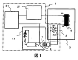
- FIG. 1 is a configuration diagram of a synchronous impulse immunity evaluation apparatus according to a first embodiment of the present invention.
- FIG. 2 is a configuration diagram of a synchronous impulse immunity evaluation apparatus according to a second embodiment of the present invention.
- FIG. 3 is a configuration diagram of a synchronous impulse immunity evaluation apparatus according to a third embodiment of the present invention.
- FIG. 4 is a configuration diagram of a synchronous impulse immunity evaluation apparatus according to a fourth embodiment of the present invention.
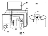
- FIG. 5 is a configuration diagram of a tester according to a fifth embodiment of the present invention provided with a synchronous impulse immunity evaluation device.
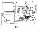
- FIG. 6 is a configuration diagram of a tester according to a sixth embodiment of the present invention provided with a synchronous impulse immunity evaluation device.
- FIG. 1 shows a configuration diagram of the synchronous impulse immunity evaluation apparatus according to the first embodiment of the present invention.
- the synchronous impulse immunity evaluation apparatus 1 includes an application probe 2, a trapezoidal wave generator 11, a controller 21, and a timing controller 31. Furthermore, an evaluation board 3 on which an electronic circuit 4 as a sample to be measured is mounted is provided.
- the electronic circuit 4 is, for example, a semiconductor integrated circuit, and includes a terminal 4A for outputting a trigger signal and a noise applying terminal 4B in FIG.
- the application probe 2 is connected from the trapezoidal wave generator 11 using a coaxial line, and includes a matching resistance R2 and an application resistance R1.
- the voltage (V) applied to the application resistor R1 is applied as a test voltage for the noise application terminal 4B.
- the sum of the resistance values of the matching resistor R2 and the applied resistor R1 is matched to the characteristic impedance of the trapezoidal wave generator 11 and the coaxial line.
- the trapezoidal wave generator 11 and the coaxial line are configured by a coaxial line having a characteristic impedance smaller than 50 ⁇ , for example, a characteristic impedance of 1 ⁇ which is the same as the applied resistance, no matching resistance is required. In this way, by matching the sum of the resistance values of the matching resistor R2 and the applied resistor R1 to the characteristic impedance, it is possible to minimize reflection at the applied probe portion and apply a rectangular wave with less noise component.
- the trapezoidal wave generation circuit 11 includes a variable power supply and a switch, and can set the peak value of the trapezoidal wave as an arbitrary voltage.
- the set voltage is supplied to the application probe 2 as an arbitrary pulse width based on the output switch control signal from the timing control device 31.
- the trapezoidal wave generator 11 is connected using a coaxial line, and a rectangular wave with less noise component can be applied.
- the rise time of the rectangular wave (trapezoidal wave) generated by the trapezoidal wave generation circuit 11 is easily realized as 1 ns or less. Therefore, on the contrary, it may be necessary to adjust the direction of extending the rise time of the trapezoidal wave, and the filter 7 is loaded in the coaxial line 6 to make the rise time variable.
- the trapezoidal wave generation circuit 11 can generate a set rectangular wave by changing the peak value, the pulse width, and the rise time of the trapezoidal wave.
- the trapezoidal wave mentioned here means a waveform generally used in a digital circuit, and is composed of a rise time, a flat region time, and a fall region time. Therefore, if the rise / fall time is very short compared to the time in the flat region, it can be treated like a rectangular wave. Conversely, a waveform in which the flat region is sufficiently shorter than the rise / fall time can be treated as a triangular wave.
- the pulse width may take the half width of the pulse, but in the description of the present invention, the rise time and the flat area corresponding to the upper base of the trapezoid are combined.
- the control device 21 includes a logic circuit or a microcomputer and has a trigger recognition function for recognizing a trigger signal.
- the control device 21 recognizes a specific output signal from the electronic circuit 4 as a trigger signal. Recognizing that the control device 21 recognizes a specific output signal from the electronic circuit 4 as a trigger signal may simply be described as a trigger signal being output from the electronic circuit 4.
- the control device 21 outputs a timer time setting signal to the timing control device and controls the timing control device.
- the timing control device 31 is a timer circuit composed of a counter, and controls the pulse width of the trapezoidal wave output from the trapezoidal wave generation device 11. For example, at the time T0 when the trigger signal from the electronic circuit 4 is output, the timer circuit starts to operate and stops at the time (T0 + Tw), so that the pulse width of the trapezoidal wave becomes Tw. This pulse width (Tw) can be arbitrarily controlled by the timer circuit of the timing control device 31. Next, the noise immunity evaluation procedure will be described.
- the circuit operation inside the electronic circuit is performed by combining various modes at various timings.
- a characteristic output in each mode is used as a trigger.
- a change in one control output or a pattern having a plurality of data lines can be extracted.
- the operation mode setting method of the electronic circuit is not particularly limited. For example, it can be set from the control device 21. Although not shown, it can be set by another device mounted on the evaluation boat or by an external pulse generator. In this embodiment, as shown in FIG. 1, the output from the terminal 4A of the electronic circuit 4 of the sample to be measured is used as a trigger, and the terminal 4B is used as the noise application terminal 4B.
- the control device 21 recognizes a specific output signal from the input terminal 4 ⁇ / b> A as a trigger signal, and outputs a timer time setting signal to the timing control device 31.
- the timing control device 31 starts the operation of the timer circuit from the time when the timer time setting signal is input, generates an output switch control signal after the set arbitrary time, and outputs it to the trapezoidal wave generator 11.
- the trapezoidal wave generator 11 supplies a trapezoidal wave having a set peak value to the application probe 2 based on the output switch control signal from the timing controller 31 and applies it to the noise application terminal 4B.
- the trapezoidal wave having the pulse width Tw is measured from the time (T0) to the measured electron. Applied to the circuit. After applying a trapezoidal wave as noise, evaluate whether the electronic circuit malfunctions.
- the evaluation method is not particularly limited. For example, the operation mode of the electronic circuit as described above is set, and whether the control device 21 outputs a normal trigger signal from the terminal 4A, or other terminals including the noise application terminal 4B are set normally. Etc. can be evaluated.
- the synchronous impulse immunity evaluation apparatus includes a trapezoidal wave generator that can change the peak value, pulse width, and rise time of a trapezoidal wave to be output, a controller that outputs a control signal, and an arbitrary timing.
- a timing control device that generates the power supply and an application probe having an application resistance; The control device outputs a timer time setting signal to the timing control device in synchronization with the trigger signal from the input electronic circuit. At a timing set by the timing control device based on the timer time setting signal, an output switch control signal is output to the trapezoidal wave generator.
- FIG. 2 shows a configuration diagram of the synchronous impulse immunity evaluation apparatus according to the second embodiment of the present invention.
- the second embodiment is a synchronous impulse immunity evaluation apparatus capable of controlling the timing of applying a trapezoidal wave at an arbitrary timing as compared with the first embodiment.
- the configuration of the synchronous impulse immunity evaluation device of the second embodiment shown in FIG. 2 is a control device 22 and a timing control device 32 instead of the control device 21 and the timing control device 31 of FIG.
- Other configurations are the same as those of the synchronous impulse immunity evaluation apparatus according to the first embodiment shown in FIG.
- the control device 22 is configured by a logic circuit or a microcomputer, and can arbitrarily control the timing of applying the trapezoidal wave to the input trigger signal, as compared with the control device 21 of the first embodiment.
- a timer time setting function has been added.
- the control device 22 has a trigger recognition function and a timer time setting function.
- a timer time setting function There are the following three cases of arbitrary timing control here.
- Application is started at time (T0 + T1) after a time (T1) is delayed from the time (T0) when the trigger signal is generated from the electronic circuit. This delaying period (T1) is controlled.
- 3) is a control by a combination of 1) and 2). Furthermore, by counting the number of times of application in combination, it is possible to successively perform malfunction determinations at various timings by slightly shifting the application timing each time.
- the trigger signal when the first trigger signal from the electronic circuit is generated, the trigger signal is applied after being delayed by the time (T1) from the time when the trigger signal is input.
- the second trigger signal When the second trigger signal is generated, it is delayed by the time (T1 + ⁇ T) from the time when the trigger signal is input, and when the (n + 1) th trigger signal is generated, the trigger signal is input.
- the voltage is applied after being delayed by the time (T1 + n ⁇ T).
- the control device 22 controls the timing control device so that a trapezoidal wave can be applied at an arbitrary time using the trigger signal / trigger pattern in this way.
- the timing control device 32 generates an output switch control signal based on the timer time setting signal from the control device 22 and outputs it to the trapezoidal wave generator 11.
- the timing control device 32 when the timer time setting signal from the control device 22 is input at the time (T1), the timing control device 32 rises at the time (T1) and sets the output switch control signal of the pal width (Tw) as a trapezoidal wave. Output to the generator 11. At this time, the timing control device 32 can also change the timer time based on the timer time setting signal and control the pulse width (Tw) of the output switch control signal to be output. The timing control device 32 can control the rise time of the trapezoidal wave using the filter 7. The trapezoidal wave generator 11 applies a trapezoidal wave to the measured electronic circuit based on the input output switch control signal from the timing controller 32.
- the synchronous impulse immunity evaluation apparatus of the second embodiment has a timer time setting function that can arbitrarily control the timing of applying a trapezoidal wave to the trigger signal.
- a trapezoidal wave can be applied to the measured electronic circuit at an arbitrary time using the trigger signal / trigger pattern.
- the trapezoidal wave application start time, pulse width, and rise time can be controlled. Therefore, the immunity characteristic of the electronic circuit can be evaluated at each time ( ⁇ T) slightly delayed from the operation timing of the electronic circuit. For this reason, it is possible to reliably detect a malfunction that occurs at a specific timing. In addition, once the malfunction timing becomes obvious, the same malfunction can be reliably caused any number of times.
- the block diagram of the synchronous impulse immunity evaluation apparatus in the 3rd Embodiment of this invention is shown in FIG.
- the third embodiment is a synchronous impulse immunity evaluation apparatus that can arbitrarily control the voltage and polarity of a trapezoidal wave as compared with the second embodiment.
- the configuration of the synchronous impulse immunity evaluation apparatus of the third embodiment shown in FIG. 3 is a control apparatus 23 and a trapezoidal wave generation apparatus 12 instead of the control apparatus 22 and the trapezoidal wave generation apparatus 11 of FIG.
- a polarity control device 41 is added and provided.
- the other configuration is the same as that of the synchronous impulse immunity evaluation apparatus of the second embodiment shown in FIG.
- the control device 23 is configured by a logic circuit or a microcomputer, and an applied voltage / polarity setting function capable of arbitrarily controlling the trapezoidal wave voltage and polarity is added as compared with the control device 22 of the second embodiment. Yes. That is, the control device 23 has a trigger recognition function, a timer time setting function, and an applied voltage / polarity setting function. When the trigger signal from the electronic circuit is input, the control device 23 outputs a timer time setting signal to the timing control device 32 and also applies a trapezoidal wave voltage (applied voltage to the applied voltage / polarity control device 41).
- the applied voltage / polarity setting signal that controls the crest voltage and polarity is output. This applied voltage / polarity setting signal is also output based on the output timing of the trigger signal.
- the applied voltage / polarity control device 41 electrically controls the voltage setting of the trapezoidal wave generator 12, and is a circuit that controls the voltage value and the positive / negative polarity with an applied voltage / polarity setting signal from the control device.
- the set trapezoidal wave is applied to the electronic circuit based on the output switch control signal from the timing control device 32.
- the trapezoidal wave setting of the trapezoidal wave generator 12 is automated using the applied voltage / polarity controller 41. By automating, it is possible to automatically detect the immunity level (the lowest voltage level at which malfunction occurs).
- the applied voltage is gradually increased, and a voltage at which a malfunction occurs can be evaluated as an immunity level.
- the peak value of the trapezoidal wave applied in the case of the first trigger signal is V
- the peak value of the trapezoidal wave applied in the case of the (n + 1) th trigger signal is (V + n ⁇ V).
- gradually increasing the peak value of the trapezoidal wave applied continuously is (V + n ⁇ V).
- the peak value of the trapezoidal wave that malfunctions first becomes the immunity level of the electronic circuit.
- the synchronous impulse immunity evaluation apparatus of the third embodiment can arbitrarily control the timing of applying a trapezoidal wave to the trigger signal, and can arbitrarily control the peak value and polarity of the trapezoidal wave to be applied.
- the applied voltage can be controlled to an arbitrary voltage in addition to the application timing.
- the applied voltage can be gradually increased, and the minimum voltage level at which a malfunction occurs can be automatically detected as the immunity level.
- the fourth embodiment is a synchronous impulse immunity evaluation device provided with a communication line capable of exchanging data between the control device of the evaluation device and the electronic circuit as compared with the third embodiment.
- the control device is additionally provided with an electronic circuit setting monitoring function capable of monitoring the loading of a program to the electronic circuit and the state of the electronic circuit as compared with the third embodiment.
- the control device 24 includes a logic circuit or a microcomputer, and includes a communication line 5 between the control device 24 and the electronic circuit 4.
- the control device 24 automatically performs various settings used for immunity evaluation, and realizes simple evaluation in a short time.
- the control device 24 recognizes the trigger signal and controls the timing control device 32 and the applied voltage / polarity control device 41.
- control device 24 communicates with the electronic circuit 4 to be evaluated, so that a test program and a test vector can be flowed into the electronic circuit 4 and the operation mode of the electronic circuit can be actively set to the test mode.
- it is possible to monitor the operating state in the electronic circuit thereby making it possible to determine a malfunction. It is also possible to keep a log of the operation in the electronic circuit and take it up at an appropriate timing after a malfunction.
- a so-called on-chip oscilloscope that monitors the waveform in the electronic circuit chip is incorporated in the electronic circuit chip to be evaluated, and the propagation waveform of the applied trapezoidal wave in the electronic circuit chip can be observed. Become.
- the electronic circuit 4 to be evaluated is an electronic circuit in which a complicated operation mode appears by a program such as a microcomputer.
- the controller 24 determines whether the test program can be run or the test vector can be loaded. For products that are currently under development, it is better to create a dedicated immunity test program that extracts the immunity evaluation part based on the product function test program, etc., and incorporates malfunction judgment conditions. Efficiency goes up.
- the control device 24 sets these test programs and test vectors in the electronic circuit.
- the control device 24 recognizes the trigger signal from the electronic circuit 4 and uses the timing control device 32 to set the trapezoidal wave application timing, rise time, and the like. Further, the control device 24 uses the applied voltage / polarity control device 41 to set the polarity and peak value of the trapezoidal wave.
- trapezoidal wave application timings are sequentially applied at intervals of ⁇ T to detect a timing at which a malfunction occurs. If a malfunction occurs, reset the electronic circuit, return it to its initial state, and start by loading the test program. The voltage and polarity of the trapezoidal wave starts from the previous values, and the next application timing is set to apply the trapezoidal wave. When application is completed within the set timer time, the voltage condition is changed.
- the synchronous impulse immunity evaluation apparatus of the fourth embodiment can communicate with an electronic circuit, and can easily set the electronic circuit and monitor the state of the electronic circuit.
- the synchronous impulse immunity evaluation apparatus can positively set the state of the electronic circuit to be evaluated in the test mode and monitor the state to determine the next application condition.
- An operation test condition such as a test program or a test vector can be given from the control device to the electronic circuit to be evaluated.
- FIG. 5 shows a configuration diagram of a tester combined with a synchronous impulse immunity evaluation apparatus.
- the fifth embodiment is a tester including any one of the above-described synchronous impulse immunity evaluation apparatuses according to the first to fourth embodiments.
- the control device 51 is composed of a logic circuit or a microcomputer and has a trigger recognition function, a timer time setting function, an applied voltage / polarity setting function, and an electronic circuit setting monitor function, and includes a timing control device and an applied voltage / polarity control device. It has both functions.
- a plurality of test cards 52 are provided for supplying a test signal to each terminal of the electronic circuit, and each of them includes a trapezoidal wave generator 54 for impulse immunity evaluation together with an input / output driver circuit 55 for a normal tester.
- the trapezoidal wave generator 54 sets the applied voltage and its polarity by the applied voltage / polarity setting signal, and the application timing of the trapezoidal wave is controlled by the output switch signal.
- a trapezoidal wave is applied to a terminal of an electronic circuit via an applied resistor R1 having the same resistance value as the characteristic impedance of the coaxial path.
- a filter capable of controlling the rise time of the trapezoidal wave is loaded in the coaxial line.
- An electronic circuit to be measured can be mounted on the motherboard 53, and each terminal of the electronic circuit is connected to a signal line of each test card via the wiring of the motherboard.
- the operation mode of the electronic circuit is set by a signal from the test card, and the noise immunity of the electronic circuit is evaluated by applying the supplied trapezoidal wave to the terminal to be measured.
- Electronic circuit setting monitoring functions such as loading test programs and test vectors into the electronic circuit and monitoring the operating state in the electronic circuit are performed via the respective input / output drivers 55.
- the procedure of immunity evaluation in the tester is the same as the procedure of the fourth embodiment.
- a test program is loaded on the electronic circuit and set to the test mode.
- the control device 51 recognizes the trigger signal from the electronic circuit, and sets the trapezoidal wave application timing, the rise time, and the like. Furthermore, the control device 51 sets the polarity, peak value, etc. of the trapezoidal wave.
- the trapezoidal wave generator 54 applies the trapezoidal wave according to the set trapezoidal wave application timing.
- the control device 51 monitors malfunction, and when malfunction occurs, resets the circuit, returns to the initial state, and starts with loading of the test program. In this way, another test program is run and the same evaluation is performed. By automatically performing a series of evaluations in this way, it is possible to grasp the overall evaluation range at which timing and how much noise is applied when malfunction occurs. Of course, only a part of this can be executed.
- the fifth embodiment is an embodiment in which a synchronous impulse immunity evaluation device is combined with a tester.
- a trapezoidal wave generator is incorporated in each card equipped with a driver, and a controller that controls the driver controls the generation of trapezoidal waves.
- FIG. 6 shows a configuration diagram of a tester combined with a synchronous impulse immunity evaluation apparatus.
- the sixth embodiment is an embodiment in which the position of the application probe for applying the trapezoidal wave shown in the tester of the fifth embodiment is closer to the electronic circuit (LSI) than on the test card of the LSI tester.
- the tester shown in FIG. 6 includes a control device 51, a test card 52, a mother board 53, and a trapezoid generator 54.
- the mother board 53 further includes a daughter board 56, and the daughter board 56 is provided with an LSI directly mountable or a socket for mounting the LSI.
- an application resistor for applying an impulse from the trapezoidal generator is mounted on the daughter board 56 in the immediate vicinity of the LSI, so that the impulse can be applied.
- the trapezoidal generator 54 is provided individually rather than inside the test card 52 so that it can be brought closer to the LSI.
- the other components are the same as those in the fifth embodiment, are denoted by the same reference numerals, and the description thereof is omitted. However, it will be understood that the same operations and effects as those in the fifth embodiment can be obtained.
- the position of the application probe is closer to the LSI, and a trapezoidal wave is applied to the LSI.
- a trapezoidal wave with less noise component is applied to the LSI, and an effect that can be tested more accurately is obtained.
- a daughter board 56 is further provided on the mother board 53, and an application probe is attached to the daughter board 56.
- the application probe can be directly mounted on the mother board 53.
- the noise evaluation of the tester can be performed automatically.
- a feature of the present invention is that a trapezoidal wave that becomes a noise pulse can be applied at an arbitrary timing in accordance with the circuit operation of the electronic circuit. If the normal output pattern is known, it is possible to detect a malfunction by detecting a case that does not match the normal output pattern. Immunity evaluation can be automated by gradually tightening the application conditions until malfunction occurs.
- a trapezoidal wave generating device that outputs a trapezoidal wave, a control device that outputs a control signal, and a timing control device that generates an arbitrary timing are provided, and the control device receives a signal from the electronic circuit under measurement.
- a timer time setting signal is output at a timing linked to the trigger signal input timing, and a timing control device outputs an output switch control signal based on the input timer time setting signal, generating a trapezoidal wave
- a synchronous impulse immunity evaluation device that applies a trapezoidal wave to the electronic circuit under measurement based on the output switch control signal input by the apparatus and evaluates the presence or absence of malfunction of the electronic circuit under measurement is obtained.
- the control device of the synchronous impulse immunity evaluation device can count the number of trigger signals, vary the timer time setting signal according to the count number, and vary the timing of applying the trapezoidal wave to the electronic circuit to be measured. .
- control device counts the number of trigger signals, changes the applied voltage / polarity setting signal output to the applied voltage / polarity control device according to the counted number, and the peak value of the trapezoidal wave output from the trapezoidal wave generator Further, at least one of the pulse width and the rise time may be varied.
- control device and the electronic circuit to be measured are connected by a communicable communication line, the control device gives a test vector for evaluation to the electronic circuit to be measured, sets the electronic circuit to be measured to the test mode, and measures The trapezoidal wave is applied to the electronic circuit based on the control from the control device, the presence or absence of the malfunction is evaluated, and the control device can obtain the malfunction determination information from the measured electronic circuit.
- a coaxial line is formed between the trapezoidal wave generator and the electronic circuit to be measured, and the end of the coaxial line is matched so that the sum of the resistance values becomes equal to the characteristic impedance of the coaxial line.
- a trapezoidal wave which is constituted by an application probe having a resistance and an application resistance and is supplied to the application resistance, is applied to the electronic circuit to be measured. Furthermore, a filter for correcting the rise time of the trapezoidal wave can be inserted on the coaxial line.
- a specific signal from the measured electronic circuit is recognized as a trigger signal, a trapezoidal wave is output at an arbitrary timing from the trigger signal, a trapezoidal wave is applied to the measured electronic circuit, and the measured electronic circuit
- a synchronous impulse immunity evaluation method for evaluating whether or not there is a malfunction is obtained.
- the number of trigger signals can be counted, and the timing at which a trapezoidal wave is output from each trigger signal can be varied according to the number of counts.
- at least one of the peak value, the pulse width, and the rise time of the trapezoidal wave to be output may be varied according to the number of counts.
- the synchronous impulse immunity evaluation apparatus of the present invention can apply a trapezoidal wave that becomes a noise pulse at an arbitrary timing in accordance with the circuit operation of the electronic circuit.
- the synchronous impulse immunity evaluation apparatus according to the present invention it is possible to evaluate immunity by applying a trapezoidal wave at any timing in various operation modes.
- this invention can provide the synchronous impulse immunity evaluation method provided with such an operation procedure, and the tester incorporating these synchronous impulse immunity evaluation apparatuses.
- Immunity evaluation using a synchronous impulse immunity evaluation device, evaluation method, and tester as described above can accurately identify improvements in the immunity of the electronic circuit being evaluated, enabling development of electronic circuits in a short period of time. It becomes.
- the embodiments of the present invention are listed below.
- a trapezoidal wave generating device that outputs a trapezoidal wave, a control device that outputs a control signal, and a timing control device that generates an arbitrary timing
- the control device recognizes a signal from the electronic circuit under measurement as a trigger signal, outputs a timer time setting signal at a timing linked to the input timing of the trigger signal, and the timer time setting signal to which the timing control device is input
- the trapezoidal wave generator applies a trapezoidal wave to the electronic circuit to be measured based on the input switch control signal, and whether or not the electronic circuit to be measured has malfunctioned.
- a synchronous impulse immunity evaluation apparatus characterized by evaluating.
- the control device counts the number of the trigger signals, varies the timer time setting signal according to the count number, and varies the timing of applying the trapezoidal wave to the electronic circuit to be measured.
- the control device and the electronic circuit to be measured are connected by a communicable communication line, the control device gives an evaluation test vector to the electronic circuit to be measured, and the electronic circuit to be measured is tested
- the mode is set, a trapezoidal wave is applied to the measured electronic circuit based on the control from the control device, the presence or absence of malfunction is evaluated, and the control device obtains malfunction determination information from the measured electronic circuit.
- the synchronous impulse immunity evaluation apparatus according to any one of (1) to (3), wherein: (5) A trapezoidal wave transmission line between the trapezoidal wave generator and the electronic circuit to be measured is formed by a coaxial line, and the terminal portion of the coaxial line has a sum of resistance values characteristic impedance of the coaxial line.
- the synchronous impulse immunity evaluation apparatus according to any one of the above.
- the trapezoidal wave transmission line in the trapezoidal wave generator is connected by a coaxial line, and a filter for correcting the rise time of the trapezoidal wave is inserted on the coaxial line.
- the synchronous impulse immunity evaluation apparatus according to any one of (5).
- a control device a test card provided with an input / output driver circuit and a trapezoidal wave generator, and a motherboard on which a measured electronic circuit can be mounted,
- the terminals of the measured electronic circuit mounted on the motherboard are connected to the signal lines of the respective test cards, the control device loads a test vector into the measured electronic circuit, and the control device reads the measured electronic circuit.
- the trapezoidal wave generator applies the trapezoidal wave to the measured electronic circuit at an arbitrary timing from the trigger signal, and evaluates the presence or absence of malfunction of the measured electronic circuit. A tester.
Landscapes
- Engineering & Computer Science (AREA)
- General Engineering & Computer Science (AREA)
- Physics & Mathematics (AREA)
- General Physics & Mathematics (AREA)
- Tests Of Electronic Circuits (AREA)
Abstract
電子回路の動作と、ノイズインパルスの印加タイミングが連動していない。このためインパルスの印加は確率的にしかできず、誤動作メカニズムとの対応が取れないという問題がある。 評価対象の電子回路内で発生する信号を、ノイズインパルス印加のタイミングのトリガーとして用いる。タイマーで印加するタイミングをさらに可変し、電子回路に印加することで、電子回路のノイズイミュニティを評価する。
Description
本発明は、矩形波をノイズとしたときの電子回路のノイズイミュニティ(ノイズ耐性)を評価する評価装置に関するものである。
軽薄短小化の進展に伴い、電子回路の集積化がすすみ、LSIの製造プロセスが微細化されるにつれ、電源電圧が減少し、相対的に電子回路(LSI)はノイズに弱くなってきている。電子回路のノイズイミュニティ(ノイズ耐性)を十分に把握して市場投入前にさまざまな対策を講じておく必要がある。
従来のインパルスに対するイミュニティ試験としてはIEC(International Electrotechnical Commission 国際電気標準会議)で設定されたIEC61000−4−2(非特許文献1)に代表される静電気放電試験が一般的である。この静電気放電試験では、一般に、電子回路に印加される波形は、振動波形になっている場合が多く、実際に電子回路に印加される電圧が規定できない。また、正極性で印加しても、実際に正側の振動で誤動作したのか、負側に振れた際に誤動作したのかは分からない。この問題を解決する為に、TLP(Transmission Line Pulse)の発生装置を使って、評価対象の電子回路に矩形波(台形波)を印加できる評価装置が開発されている。本装置は、高圧電源と、同軸線路とスイッチから成り、同軸線路に準静的に電荷を貯めておき、スイッチをONにすることにより、その先の線路に、立ち上がり時間の短い、台形波を印加できるものである。その場合のパルス幅(フラットな領域)は同軸線路の長さによって決まる。
また特許2718068号公報(特許文献1)には、振幅制御された台形波発生装置、およびタイマーによって波形パラメータをコントロールする手法が記載されている。さらに特開2000−304794号公報(特許文献2)には、イミュニティ試験方法として、パルスの波高値を可変しながら印加し、異常発生所の印加レベルをイミュニティとする合否判定法が記載されている。
従来のインパルスに対するイミュニティ試験としてはIEC(International Electrotechnical Commission 国際電気標準会議)で設定されたIEC61000−4−2(非特許文献1)に代表される静電気放電試験が一般的である。この静電気放電試験では、一般に、電子回路に印加される波形は、振動波形になっている場合が多く、実際に電子回路に印加される電圧が規定できない。また、正極性で印加しても、実際に正側の振動で誤動作したのか、負側に振れた際に誤動作したのかは分からない。この問題を解決する為に、TLP(Transmission Line Pulse)の発生装置を使って、評価対象の電子回路に矩形波(台形波)を印加できる評価装置が開発されている。本装置は、高圧電源と、同軸線路とスイッチから成り、同軸線路に準静的に電荷を貯めておき、スイッチをONにすることにより、その先の線路に、立ち上がり時間の短い、台形波を印加できるものである。その場合のパルス幅(フラットな領域)は同軸線路の長さによって決まる。
また特許2718068号公報(特許文献1)には、振幅制御された台形波発生装置、およびタイマーによって波形パラメータをコントロールする手法が記載されている。さらに特開2000−304794号公報(特許文献2)には、イミュニティ試験方法として、パルスの波高値を可変しながら印加し、異常発生所の印加レベルをイミュニティとする合否判定法が記載されている。
上記したTLP発生装置を使った評価装置として、本願発明者により出願されたWO 2008/108503 A1(特許文献3)がある。特許文献3では、TLP発生装置を用い、正方向、負方向のみの矩形波を印加し、誤動作のレベルを正確に知る技術が開示されている。しかし特許文献3では、ノイズが評価対象の電子回路に印加されるタイミングはコントロールできない。そのため従来のESD(electrostatic discharge)ガンでの印加と同様、動作のどのタイミングでインパルスが印加されるかは分からなかった。このように電子回路の動作と、ノイズインパルスの印加タイミングが連動していない。このため、誤動作する時間範囲が非常に短い場合、その時間範囲にインパルスが印加される確率が非常に低くなり、数百回~数千回に1回程度の誤動作確率になることもある。この場合、誤動作の評価に時間がかかるという課題があった。そのためにインパルスを印加するタイミングを制御できるノイズイミュニティ評価装置の開発が望まれている。
本発明は、上記した課題を解決するためになされたものであって、評価対象の電子回路の動作タイミングに連動した特定のタイミングで、電子回路にインパルスを印加する同期型インパルスイミュニティ評価装置を提供するものである。
本発明は、上記した課題を解決するためになされたものであって、評価対象の電子回路の動作タイミングに連動した特定のタイミングで、電子回路にインパルスを印加する同期型インパルスイミュニティ評価装置を提供するものである。
本発明の同期型インパルスイミュニティ評価装置は、台形波を出力する台形波発生装置と、制御信号を出力する制御装置と、任意のタイミングを発生するタイミングコントロール装置と、を備えている。前記制御装置が被測定電子回路からの信号をトリガー信号として認識し、前記トリガー信号の入力タイミングに連動したタイミングにタイマー時間設定信号を出力し、前記タイミングコントロール装置が入力された前記タイマー時間設定信号に基づいて出力スイッチ制御信号を出力し、前記台形波発生装置が入力された前記出力スイッチ制御信号に基づいて前記被測定電子回路に台形波を印加し、前記被測定電子回路の誤動作の有無を評価することを特徴とする。
本発明のテスターは、制御装置と、入出力ドライバ回路と台形波発生装置とが設けられたテストカードと、被測定電子回路が装着可能なマザーボードと、を備え、前記マザーボードに装着された被測定電子回路の端子は、それぞれのテストカードの信号線に接続され、前記制御装置が前記被測定電子回路にテストベクトルをロードし、前記制御装置が前記被測定電子回路からの信号をトリガー信号と認識し、前記台形波発生装置が前記トリガー信号から任意のタイミングで台形波を前記被測定電子回路印加し、前記被測定電子回路の誤動作の有無を評価することを特徴とする。
本発明の同期型インパルスイミュニティ評価方法は、被測定電子回路からの特定信号をトリガー信号として認識し、前記トリガー信号から任意のタイミングで台形波を出力し、前記台形波を前記被測定電子回路に印加し、前記被測定電子回路の誤動作の有無を評価することを特徴とする。
本発明のテスターは、制御装置と、入出力ドライバ回路と台形波発生装置とが設けられたテストカードと、被測定電子回路が装着可能なマザーボードと、を備え、前記マザーボードに装着された被測定電子回路の端子は、それぞれのテストカードの信号線に接続され、前記制御装置が前記被測定電子回路にテストベクトルをロードし、前記制御装置が前記被測定電子回路からの信号をトリガー信号と認識し、前記台形波発生装置が前記トリガー信号から任意のタイミングで台形波を前記被測定電子回路印加し、前記被測定電子回路の誤動作の有無を評価することを特徴とする。
本発明の同期型インパルスイミュニティ評価方法は、被測定電子回路からの特定信号をトリガー信号として認識し、前記トリガー信号から任意のタイミングで台形波を出力し、前記台形波を前記被測定電子回路に印加し、前記被測定電子回路の誤動作の有無を評価することを特徴とする。
本発明の同期型インパルスイミュニティ評価装置は、被測定電子回路からの信号をトリガー信号として台形波を出力し、被測定電子回路に印加することでノイズイミュニティを評価する。被測定電子回路からの信号をトリガー信号とすることで、被測定電子回路の動作タイミングと電子回路にインパルス(台形波)を印加するタイミングとを関連させ、連動させることができる。本発明によれば、台形波を電子回路の回路動作にあわせて任意なタイミングで印加できる同期型インパルスイミュニティ評価装置が得られる。
図1は、本発明の第1実施形態による同期型インパルスイミュニティ評価装置の構成図である。
図2は、本発明の第2実施形態による同期型インパルスイミュニティ評価装置の構成図である。
図3は、本発明の第3実施形態による同期型インパルスイミュニティ評価装置の構成図である。
図4は、本発明の第4実施形態による同期型インパルスイミュニティ評価装置の構成図である。
図5は、同期型インパルスイミュニティ評価装置を備えた本発明の第5実施形態によるテスターの構成図である。
図6は、同期型インパルスイミュニティ評価装置を備えた本発明の第6実施形態によるテスターの構成図である。
図2は、本発明の第2実施形態による同期型インパルスイミュニティ評価装置の構成図である。
図3は、本発明の第3実施形態による同期型インパルスイミュニティ評価装置の構成図である。
図4は、本発明の第4実施形態による同期型インパルスイミュニティ評価装置の構成図である。
図5は、同期型インパルスイミュニティ評価装置を備えた本発明の第5実施形態によるテスターの構成図である。
図6は、同期型インパルスイミュニティ評価装置を備えた本発明の第6実施形態によるテスターの構成図である。
次に、本発明の実施の形態を、図面を参照して詳細に説明する。本発明の同期型インパルスイミュニティ評価装置は、被測定サンプルの電子回路の動作タイミングをトリガーとして、台形波の印加タイミングを可変とし、電子回路の動作中の特定位置での誤動作を検出することを特徴とするものである。
(第1の実施形態)
本発明の第1の実施の形態における同期型インパルスイミュニティ評価装置の構成図を図1に示す。図1に示すように同期型インパルスイミュニティ評価装置1は、印加プローブ2、台形波発生装置11、制御装置21、タイミングコントロール装置31を備える。さらに被測定サンプルとしての電子回路4が搭載された評価用ボード3を備えている。電子回路4は、例えば半導体集積回路であり、図1ではトリガー信号を出力する端子4A、ノイズ印加端子4Bを備えている。
印加プローブ2は、台形波発生装置11から同軸線路を用いて接続され、整合抵抗R2と、印加抵抗R1から構成される。印加抵抗R1にかかる電圧(V)が、ノイズ印加端子4Bの試験電圧として印加されることになる。整合抵抗R2と印加抵抗R1の抵抗値の和は台形波発生装置11及び同軸線路の特性インピーダンスに合わせる。一般的に、50Ωの特性インピーダンスをもつ同軸線路が用いられているため、例えば整合抵抗R2は49Ω、印加抵抗R1は1Ωとして実現する。すなわち、整合抵抗値=特性インピーダンス値−印加抵抗値として設定する。しかし、50Ωよりも小さな特性インピーダンス、例えば、印加抵抗と同じ1Ωの特性インピーダンスの同軸線路で台形波発生装置11及び同軸線路を構成すれば、整合抵抗は要らない。このように整合抵抗R2と印加抵抗R1の抵抗値の和を特性インピーダンスに合わせることで、印加プローブ部での反射を最小限に抑え、ノイズ成分の少ない矩形波を印加することができる。
台形波発生回路11は、可変電源とスイッチを備え、台形波の波高値を任意の電圧として設定できる。設定された電圧をタイミングコントロール装置31からの出力スイッチ制御信号に基づいて任意のパルス幅として、印加プローブ2に供給する。台形波発生装置11からは同軸線路を用いて接続され、ノイズ成分の少ない矩形波を印加することができる。台形波発生回路11で生成される矩形波(台形波)の立ち上がり時間としては、一般的に1ns以下が容易に実現される。そのため逆に、台形波の立ち上がり時間を伸ばす方向の調整が必要な場合があり、同軸線路6内にフィルタ7を装荷し、立ち上がり時間を可変とする。フィルタ7を用いる場合には、2ns~100ns、あるいは、それ以上の立ち上がり時間を実現することができる。このように台形波発生回路11は、台形波の波高値、パルス幅及び立ち上がり時間を可変し、設定された矩形波を発生することができる。
ここで言う台形波は、デジタル回路で一般に用いられる波形を意味しており、立ち上り時間、フラット領域の時間、立下がり領域の時間で構成される。従って、立ち上り/立下り時間がフラット領域の時間に比べ非常に短ければ矩形波のように扱うことが出来る。逆に、フラット領域が、立ち上り/立下り時間に比べ充分に短い波形は三角波として扱うことが出来るものである。パルス幅はパルスの半値幅をとる場合もあるが、本発明の説明の中では立ち上がり時間と、台形の上底に相当するフラットな領域を合わせた時間とする。
制御装置21は、ロジック回路又はマイクロコンピュータで構成され、トリガー信号を認識するトリガー認識機能を有する。制御装置21は、電子回路4からの特定の出力信号をトリガー信号と認識する。この制御装置21が電子回路4からの特定の出力信号をトリガー信号として認識することを、単に、電子回路4からトリガー信号が出力されると記載することがある。制御装置21は、タイマー時間設定信号をタイミングコントロール装置に出力し、タイミングコントロール装置をコントロールする。図では電子回路4からのトリガー信号は一本として示しているが、複数本の信号の組み合わせからトリガー信号を抽出し、タイマー時間設定信号を設定してもよい。タイミングコントロール装置31は、カウンタから成るタイマー回路であり、台形波発生装置11から出力される台形波のパルス幅を制御する。例えば電子回路4からのトリガー信号が出力される時刻T0において、タイマー回路が動作スタートし、時刻(T0+Tw)で停止することで、台形波のパルス幅はTwとなる。このパルス幅(Tw)は、タイミングコントロール装置31のタイマー回路により、任意に制御することが出来る。
次に、ノイズイミュニティ評価の手順について説明する。電子回路内部の回路動作は、様々なモードが様々なタイミングで組み合わされて動作している。この各モードで特徴的な出力をトリガーとする。この出力としては、1本のコントロール出力の変化や、複数のデータ線路のあるパターンを抽出することができる。また、この電子回路の動作モード設定方法は特に限定されない。例えば、制御装置21から設定することができる。さらに図示していないが、評価ボートに搭載した他のデバイスや、あるいは外部からのパルス発生器により設定することができる。本実施形態では、図1に示すように、被測定サンプルの電子回路4の端子4Aからの出力をトリガーとし、端子4Bをノイズ印加端子4Bとしている。
制御装置21は、入力された端子4Aからの特定の出力信号をトリガー信号として認識し、タイミングコントロール装置31にタイマー時間設定信号を出力する。タイミングコントロール装置31は、タイマー時間設定信号が入力された時間からタイマー回路が動作開始し、設定された任意の時間後に出力スイッチ制御信号を生成し、台形波発生装置11に出力する。台形波発生装置11は設定された波高値をもつ台形波を、タイミングコントロール装置31からの出力スイッチ制御信号に基づいて印加プローブ2に供給し、ノイズ印加端子4Bに印加する。ここで、電子回路からトリガー信号が発生される時刻をT0、タイミングコントロール装置31のタイマー期間(遅延時間)をTwとした場合には、パルス幅Twの台形波が時刻(T0)から被測定電子回路に印加される。
ノイズとして台形波を印加後に、電子回路が誤動作するかを評価する。評価方法としては特に限定されない。例えば、上記したような電子回路の動作モードを設定し、制御装置21が、端子4Aから正常なトリガー信号が出力されるか、あるいはノイズ印加端子4Bを含めた他端子が正常に設定されるか等で評価することができる。このようにして、あるモードで動作中の特定のタイミング位置での誤動作(例えばクロックの変化点前後で誤動作が発生する等)を検出することが出来る。
第1の実施形態の同期型インパルスイミュニティ評価装置は、出力する台形波の波高値、パルス幅及び立ち上がり時間を可変可能な台形波発生装置と、制御信号を出力する制御装置と、任意のタイミングを発生するタイミングコントロール装置と、印加抵抗を有する印加プローブと、を備える。制御装置が入力された電子回路からのトリガー信号に同期して、タイミングコントロール装置にタイマー時間設定信号を出力する。タイミングコントロール装置がタイマー時間設定信号に基づいて設定されたタイミングにおいて、台形波発生装置に出力スイッチ制御信号を出力する。台形波発生装置が設定された台形波を印加プローブの印加抵抗を介して電子回路の被測定端子に印加し、電子回路の誤動作の有無の評価が可能になる。
このように、電子回路の各モードで特徴的な出力をトリガーにして、その時間からタイマーを任意な時間にセットし、台形波の印加タイミングを任意に異ならせる。これにより、あるモードで動作中の特定の位置での誤動作(例えばクロックの変化点前後で誤動作が発生する等)を検出することが出来るという効果が得られる。
(第2の実施形態)
本発明の第2の実施形態における同期型インパルスイミュニティ評価装置の構成図を図2に示す。第2の実施形態は、第1の実施形態に比較して台形波を印加するタイミングを任意タイミングに制御可能とした同期型インパルスイミュニティ評価装置である。図2に示す第2の実施形態の同期型インパルスイミュニティ評価装置の構成は、図1の制御装置21及びタイミングコントロール装置31の代わりに、制御装置22及びタイミングコントロール装置32となっている。他の構成は図1に示す第1の実施形態の同期型インパルスイミュニティ評価装置と同様であり、同じ符号としその説明は省略する。
制御装置22は、ロジック回路又はマイクロコンピュータで構成され、第1の実施形態の制御装置21に比較して、さらに入力されるトリガー信号に対して、台形波を印加するタイミングを任意にコントロール可能なタイマー時間設定機能が追加されている。すなわち制御装置22は、トリガー認識機能とタイマー時間設定機能とを有する。ここでの任意なタイミングのコントロールには、以下の3つの場合がある。
1) トリガー信号が発生してからの印加までの時間のコントロールである。電子回路からのトリガー信号が発生される時刻(T0)から期間(T1)だけ遅らせ、時刻(T0+T1)に印加開始する。この遅らせる期間(T1)を制御する。
2) トリガーパルスを何回カウントしてから、ノイズを印加するかのコントロールである。
3)は1)と2)の組み合わせによるコントロールである。
さらに、これらを組み合わせて印加した回数をカウントすることで、毎回、印加のタイミングを少しずつずらして、様々なタイミングでの誤動作判定を連続して行うことが可能となる。例えば、電子回路からの最初のトリガー信号が発生された場合には、トリガー信号が入力された時刻から時刻(T1)だけ遅らせて、印加する。2番目のトリガー信号が発生された場合には、トリガー信号が入力された時刻から時刻(T1+△T)だけ遅らせ、(n+1)番目のトリガー信号が発生された場合には、トリガー信号が入力された時刻から時刻(T1+n△T)だけ遅らせてから、印加する。制御装置22は、このようにトリガー信号/トリガーパターンを用いて任意な時間に台形波を印加できるようにタイミングコントロール装置を制御する。
タイミングコントロール装置32は、制御装置22からのタイマー時間設定信号に基づいて出力スイッチ制御信号を生成し、台形波発生装置11に出力する。例えば、タイミングコントロール装置32は、制御装置22からのタイマー時間設定信号が時刻(T1)に入力された場合には、時刻(T1)に立ち上がり、パル幅(Tw)の出力スイッチ制御信号を台形波発生装置11に出力する。このときタイミングコントロール装置32は、タイマー時間設定信号に基づいてそのタイマー時間を可変とし、出力する出力スイッチ制御信号のパルス幅(Tw)を制御することもできる。またタイミングコントロール装置32は、フィルタ7を使って、台形波の立ち上がり時間を制御することが出来る。台形波発生装置11は、入力されたタイミングコントロール装置32からの出力スイッチ制御信号に基づいて台形波を被測定電子回路に印加する。
第2の実施形態の同期型インパルスイミュニティ評価装置は、トリガー信号に対して、台形波を印加するタイミングを任意にコントロール可能なタイマー時間設定機能を有する。トリガー信号/トリガーパターンを用いて任意な時間に台形波を被測定電子回路に印加できる。この実施形態では、台形波の印加開始時点、パルス幅、立ち上がり時間をコントロールすることが出来る。従って、電子回路の動作タイミングに対し、それぞれわずかに遅れた時刻(△T)毎に電子回路のイミュニティ特性を評価することができる。
このため、特定のタイミングで発生する誤動作を確実に検出することが出来る。また、一度誤動作するタイミングが自明になれば、何度でも同じ誤動作を確実に起すことができる。従って、誤動作した場合の内部解析が容易に行える様になり、内部の誤動作メカニズムの解明が飛躍的に加速でき、誤動作要因の分析が容易になり、ノイズイミュニティ改善に役立てることができるという効果が得られる。
(第3の実施形態)
本発明の第3の実施形態における同期型インパルスイミュニティ評価装置の構成図を図3に示す。第3の実施の形態は、第2の実施の形態に比較して台形波の電圧、極性を任意に制御可能とした同期型インパルスイミュニティ評価装置である。図3に示す第3の実施の形態の同期型インパルスイミュニティ評価装置の構成は、図2の制御装置22及び台形波発生装置11の代わりに制御装置23及び台形波発生装置12となり、さらに印加電圧・極性コントロール装置41を追加、備えている。他の構成は図2に示す第2の実施形態の同期型インパルスイミュニティ評価装置と同様であり、同じ符号としその説明は省略する。
制御装置23は、ロジック回路又はマイクロコンピュータで構成され、第2の実施形態の制御装置22に比較して、台形波の電圧、極性を任意にコントロール可能な印加電圧・極性設定機能が追加されている。すなわち制御装置23は、トリガー認識機能、タイマー時間設定機能、印加電圧・極性設定機能を有する。制御装置23は、電子回路からのトリガー信号が入力された場合には、タイミングコントロール装置32にタイマー時間設定信号を出力するとともに、印加電圧・極性コントロール装置41に印加電圧である台形波の電圧(波高電圧)及び極性を制御する印加電圧・極性設定信号を出力する。この印加電圧・極性設定信号もトリガー信号の出力タイミングに基づいて出力される。
印加電圧・極性コントロール装置41は、台形波発生装置12の電圧設定を電気的にコントロールするもので、電圧値及び正負の極性を制御装置からの印加電圧・極性設定信号でコントロールする回路である。設定された台形波がタイミングコントロール装置32からの出力スイッチ制御信号に基づき電子回路に印加される。台形波発生装置12の台形波の設定を、印加電圧・極性コントロール装置41に用いて自動化する。自動化することで、イミュニティレベル(誤動作する最低電圧レベル)の自動検出が可能となる。例えば、印加電圧を徐々に上げていき、誤動作が発生した電圧をイミュニティレベルとして評価できる。電子回路の特定端子に対して、第1のトリガー信号の場合に印加する台形波の波高値をV、第(n+1)のトリガー信号の場合に印加する台形波の波高値を(V+n△V)とし、連続して印加する台形波の波高値を徐々に高くする。このとき、最初に誤動作する台形波の波高値が電子回路のイミュニティレベルとなる。
第3の実施形態の同期型インパルスイミュニティ評価装置は、トリガー信号に対して、台形波を印加するタイミングを任意にコントロールし、さらに印加する台形波の波高値と極性を任意にコントロール可能である。つまり、印加のタイミングに加え印加電圧をも任意の電圧にコントロール可能となる。印加電圧を徐々に上げていき、誤動作が発生した最低電圧レベルをイミュニティレベルとして自動検出することが出来る効果が得られる。
(第4の実施形態)
本発明の第4の実施形態における同期型インパルスイミュニティ評価装置の構成図を図4に示す。第4の実施の形態は、第3の実施の形態に比較して評価装置の制御装置と電子回路との間でデータのやり取り可能な通信線を備えた同期型インパルスイミュニティ評価装置である。制御装置は、第3の実施の形態に比較して電子回路へのプログラムのロードや電子回路の状態をモニター可能な電子回路設定モニター機能を追加して備える。図4に示す第4の実施の形態の同期型インパルスイミュニティ評価装置の構成は、図3の制御装置23の代わりに制御装置24となり、さらに制御装置と電子回路との間で信号のやり取り可能な通信線5を備えている。他の構成は図3に示す第3の実施形態の同期型インパルスイミュニティ評価装置と同様であり、同じ符号としその説明は省略する。
制御装置24はロジック回路又はマイクロコンピュータで構成され、制御装置24と電子回路4間に通信線5を備えている。制御装置24は、イミュニティ評価に用いる様々な設定を自動で行い、短時間で簡便な評価を実現する。制御装置24は、トリガー信号を認識し、タイミングコントロール装置32、印加電圧・極性コントロール装置41をコントロールする。さらに、制御装置24は、評価対象の電子回路4と通信することで、テストプログラムやテストベクトルを電子回路4に流し込み、電子回路の動作モードを積極的にテストモードとすることが出来る。また、電子回路内の動作状態を監視することが出来、これにより、誤動作の判別が可能となる。また、電子回路内に動作のログをとっておき、誤動作後等、適当なタイミングで吸い上げることが可能である。また、電子回路チップ内の波形をモニターする、所謂、オンチップオシロスコープなどを評価対象の電子回路チップ内に組み込んでおき、印加された台形波の電子回路チップ内への伝播波形の観測が可能となる。上記した電子回路へのプログラムのロード、電子回路の状態の監視やモニター、電子回路とのデータやり取りを総称して電子回路設定モニター機能と呼ぶ。
次にノイズイミュニティ評価手順の一例を示す。ここでは、評価対象の電子回路4がマイコンなどのプログラムによって複雑な動作モードが現れる電子回路を対象にする。先ず制御装置24は、テストプログラムが走らせられるか、もしくはテストベクトルをロードできるかの判断を行う。一般的に開発中の製品であれば、製品の機能テスト用のテストプログラムなどを元に、イミュニティ評価部分を抽出し、誤動作判定条件などを盛り込んだ専用のイミュニティテストプログラムを作成するほうが、評価の効率は上がる。制御装置24は、これらテストプログラムやテストベクトルを電子回路にセットする。
次に、制御装置24は、電子回路4からのトリガー信号を認識し、タイミングコントロール装置32を使って台形波の印加タイミングや立ち上り時間などを設定する。さらに制御装置24は、印加電圧・極性コントロール装置41を使って台形波の極性、波高値などを設定する。次に、台形波の印加タイミングをΔT間隔で順に印加し誤動作が出るタイミングを検出する。誤動作が出たら、電子回路をリセットし、初期状態に戻し、テストプログラムのロードからはじめる。台形波の電圧、極性は先ほどの値から始め、次の印加タイミングをセットして台形波を印加する。設定したタイマー時間内の印加が終わったら、電圧条件を変更する。電圧条件の設定範囲を終了したら、別のテストプログラムを走らせて、同様の評価を行う。このように一連の評価を自動で行うことにより、誤動作がどのタイミングで、どれだけのノイズ電圧の印加に対して発生するかを、評価範囲全般に対して把握することが出来る。勿論この一部を切り出して行うことも可能である。
第4の実施形態の同期型インパルスイミュニティ評価装置は、電子回路との間で通信可能であり、電子回路へのセット及び電子回路の状態のモニターが簡単にできる。同期型インパルスイミュニティ評価装置は、積極的に評価対象の電子回路の状態をテストモードにセットし、その状態をモニターして、次の印加の条件を決めることができる。制御装置から評価対象の電子回路にテストプログラムや、テストベクトルといった動作試験条件を与えることが出来る。もしくは、評価対象の電子回路内の電源やグランドの電圧変動、各ノードの電圧変動、もしくは出力レベル(“H”又は“L”)の状態をモニターできる。さらに、評価対象の電子回路内にデータを蓄積して誤動作後にその状態を吸い上げたることができる。このようなイミュニティ試験として行うべき一連の動作が自動で実現でき、イミュニティ評価を自動化できる同期型インパルスイミュニティ評価装置が得られる。
(第5の実施形態)
本発明の第5の実施形態として、同期型インパルスイミュニティ評価装置を組み合わせたテスターの構成図を図5に示す。第5の実施の形態は、上記した第1から第4の実施の形態の同期型インパルスイミュニティ評価装置のいずれかを備えたテスターである。図5に示すテスター50は、制御装置51、テストカード52、マザーボード53を備えている。テスター50は通常のテスト機能を備えているが、以下、本発明に関連するノイズイミュニティに関する事項のみについて説明する。
制御装置51は、ロジック回路又はマイクロコンピュータで構成され、トリガー認識機能、タイマー時間設定機能、印加電圧・極性設定機能、電子回路設定モニター機能を有し、タイミングコントロール装置及び印加電圧・極性コントロール装置の機能を併せ持つ。テストカード52は、電子回路の各端子にテスト信号を供給するために複数備えられ、それぞれに通常テスター用の入出力ドライバ回路55とともに、インパルスイミュニティ評価用の台形波発生装置54を備えている。台形波発生装置54は、印加電圧・極性設定信号により印加電圧とその極性を設定し、出力スイッチ信号により台形波の印加タイミングがコントロールされる。図は、同軸経路の特性インピーダンスと同じ抵抗値の印加抵抗R1を介して電子回路の端子に台形波を印加している。また図示していないが同軸線路内には、台形波の立ち上がり時間を制御可能なフィルタを装荷している。
マザーボード53には被測定対象の電子回路が装着可能であり、電子回路のそれぞれの端子はマザーボードの配線を経由して、それぞれのテストカードの信号線に接続される。例えば、テストカードからの信号により電子回路の動作モードが設定され、さらに供給される台形波を被測定端子に印加することで、電子回路のノイズイミュニティを評価する。電子回路にテストプログラムやテストベクトルをロード、また電子回路内の動作状態を監視する等の電子回路設定モニター機能は、それぞれの入出力ドライバ55を経由して行われる。
テスターにおけるイミュニティ評価の手順としては、第4実施形態の実施手順と同様であり、最初に電子回路にテストプログラムをロードし、テストモードに設定する。次に、制御装置51は、電子回路からのトリガー信号を認識し、台形波の印加タイミングや、立ち上り時間などを設定する。さらに制御装置51は、台形波の極性、波高値などを設定する。次に台形波発生装置54は、設定された台形波の印加タイミングに従って、台形波を印加する。制御装置51は、誤動作を監視し、誤動作が出たら、回路をリセットし、初期状態に戻し、テストプログラムのロードからはじめる。このように別のテストプログラムを走らせて、同様の評価を行う。このように一連の評価を自動で行うことにより、誤動作がどのタイミングで、どれだけのノイズの印加に対して発生するかを、評価範囲全般に対して把握することが出来る。勿論この一部のみを実行することも可能である。
第5の実施形態は、テスターに同期型インパルスイミュニティ評価装置を組み合わせた実施形態である。ドライバを搭載した各カードに台形波発生装置を組み込み、ドライバをコントロールする制御装置が台形波の発生をコントロールする。これにより、一連の動作は、テスターのノイズ評価の一環として自動化して実施できる。
(第6の実施形態)
本発明の第6の実施形態として、同期型インパルスイミュニティ評価装置を組み合わせたテスターの構成図を図6に示す。第6の実施形態は、上記した第5実施形態のテスターに示した台形波を印加する印加プローブの位置をLSIテスターのテストカード上ではなく、より電子回路(LSI)に近づけた実施形態である。
図6に示すテスターは、制御装置51、テストカード52、マザーボード53、台形発生装置54を備えている。マザーボード53はさらにドーターボード56を備え、ドーターボード56には、LSIが直接装着可能、もしくはLSIを装着するソケットが設けられている。さらに、そのドーターボード56には、LSIの直近に台形発生装置からのインパルスを印加するための印加抵抗が装着され、インパルスを印加することができる。そのために台形発生装置54は、テストカード52の内部ではなく、個別に設けられ、よりLSIに近づけられるようにしてある。その他の構成要素は第5実施形態と同様であり、同じ符号とし、その説明は省略するが、第5実施形態と同様の動作及び効果が得られることは理解できるであろう。
第6の実施形態では、印加プローブの位置をよりLSIに近づけ、台形波をLSIに印加している。そのためLSIには、ノイズ成分の少ない台形波が印加され、より精確にテストできる効果が得られる。また、ここではマザーボード53にさらにドーターボード56を設け、そのドーターボード56に印加プローブを装着した。しかし、マザーボード53に直接印加プローブを装着することもできる。このように第6の実施形態においても、テスターのノイズ評価を自動化して実施できる。
本発明の特徴は、ノイズパルスとなる台形波を電子回路の回路動作にあわせて任意なタイミングで印加できることにある。正常な出力パターンが分かっていれば、それと合わない場合を検出して誤動作検出が可能である。誤動作になるまで、印加の条件を徐々に厳しくするという、イミュニティ評価の自動化が可能となる。評価対象がプログラム変更可能な電子回路等の場合はテストプログラム、もしくはテストベクトルを書き換えながら、実働時に現れるモードを順番にロードして、その任意なタイミングで任意なレベルの台形波を印加することが可能である。ノイズイミュニティ評価を自動で検査することが可能となる。さらに同期型インパルスイミュニティ評価装置を、LSIテスターに組み込むことも可能である。
本発明によれば、台形波を出力する台形波発生装置と、制御信号を出力する制御装置と、任意のタイミングを発生するタイミングコントロール装置と、を備え、制御装置が被測定電子回路からの信号をトリガー信号として認識し、トリガー信号の入力タイミングに連動したタイミングにタイマー時間設定信号を出力し、タイミングコントロール装置が入力されたタイマー時間設定信号に基づいて出力スイッチ制御信号を出力し、台形波発生装置が入力された出力スイッチ制御信号に基づいて被測定電子回路に台形波を印加し、被測定電子回路の誤動作の有無を評価する同期型インパルスイミュニティ評価装置が得られる。
同期型インパルスイミュニティ評価装置の制御装置は、トリガー信号の数をカウントし、そのカウント数に応じてタイマー時間設定信号を可変し、被測定電子回路に台形波を印加するタイミングを異ならせることができる。また制御装置は、トリガー信号の数をカウントし、そのカウント数に応じて印加電圧・極性コントロール装置に出力する印加電圧・極性設定信号を可変し、台形波発生装置から出力する台形波の波高値、パルス幅及び立ち上がり時間のうち少なくともいずれか1つを異ならせてもよい。さらに制御装置と被測定電子回路との間を通信可能な通信線で接続し、制御装置が被測定電子回路に評価用のテストベクトルを与え、被測定電子回路をテストモードに設定し、被測定電子回路に制御装置からの制御に基づいて台形波を印加し、その誤動作の有無を評価し、制御装置が被測定電子回路から誤動作判別情報を入手することができる。
同期型インパルスイミュニティ評価装置においては、台形波発生装置と被測定電子回路の間が同軸線路で形成され、その同軸線路の終端部は、その抵抗値の和が同軸線路の特性インピーダンスと等しくなる整合抵抗と印加抵抗とを備えた印加プローブにより構成され、印加抵抗に供給される台形波を被測定電子回路に印加する。さらに、その同軸線路上に台形波の立ち上がり時間を補正するフィルタが挿入することができる。
本発明においては、被測定電子回路からの特定信号をトリガー信号として認識し、そのトリガー信号から任意のタイミングで、台形波を出力し、台形波を被測定電子回路に印加し、被測定電子回路の誤動作の有無を評価する同期型インパルスイミュニティ評価方法が得られる。その同期型インパルスイミュニティ評価方法においては、トリガー信号の数をカウントし、そのカウント数に応じて、それぞれのトリガー信号から台形波を出力するタイミングを異ならせることもできる。さらに、そのカウント数に応じて、出力する台形波の波高値、パルス幅及び立ち上がり時間のうち少なくともいずれか1つを異ならせてもよい。
本発明の同期型インパルスイミュニティ評価装置は、ノイズパルスとなる台形波を電子回路の回路動作にあわせて任意なタイミングで印加できる。本発明による同期型インパルスイミュニティ評価装置を用いることで、様々な、動作モードにおける任意のタイミングに台形波を印加してイミュニティを評価することができる。さらに本発明は、このような動作手順を備えた同期型インパルスイミュニティ評価方法や、これらの同期型インパルスイミュニティ評価装置を組み込んだテスターを提供することができる。上記したような同期型インパルスイミュニティ評価装置、評価方法、テスターを用いたイミュニティ評価により、評価対象である電子回路のイミュニティの改善点を的確に捉えることができ、短期間での電子回路開発が可能となる。
以下に本発明の実施の態様を列挙する。
(1) 台形波を出力する台形波発生装置と、制御信号を出力する制御装置と、任意のタイミングを発生するタイミングコントロール装置と、を備え、
前記制御装置が被測定電子回路からの信号をトリガー信号として認識し、前記トリガー信号の入力タイミングに連動したタイミングにタイマー時間設定信号を出力し、前記タイミングコントロール装置が入力された前記タイマー時間設定信号に基づいて出力スイッチ制御信号を出力し、前記台形波発生装置が入力された前記出力スイッチ制御信号に基づいて前記被測定電子回路に台形波を印加し、前記被測定電子回路の誤動作の有無を評価することを特徴とする同期型インパルスイミュニティ評価装置。
(2) 前記制御装置が前記トリガー信号の数をカウントし、そのカウント数に応じて前記タイマー時間設定信号を可変し、前記被測定電子回路に台形波を印加するタイミングを異ならせることを特徴とする上記(1)に記載の同期型インパルスイミュニティ評価装置。
(3) 前記制御装置が前記トリガー信号の数をカウントし、そのカウント数に応じて印加電圧・極性コントロール装置に出力する印加電圧・極性設定信号を可変し、前記台形波発生装置から出力する台形波の波高値、パルス幅及び立ち上がり時間のうち少なくともいずれか1つを異ならせることを特徴とする上記(1)又は(2)に記載の同期型インパルスイミュニティ評価装置。
(4) 前記制御装置と前記被測定電子回路との間を通信可能な通信線で接続し、前記制御装置が前記被測定電子回路に評価用のテストベクトルを与え、前記被測定電子回路をテストモードに設定し、前記被測定電子回路に前記制御装置からの制御に基づいて台形波を印加し、その誤動作の有無を評価し、前記制御装置が前記被測定電子回路から誤動作判別情報を入手することを特徴とする上記(1)乃至(3)のいずれかに記載の同期型インパルスイミュニティ評価装置。
(5) 前記台形波発生装置と前記被測定電子回路との間の台形波の伝送線は同軸線路で形成され、その同軸線路の終端部は、その抵抗値の和が前記同軸線路の特性インピーダンスと等しくなる整合抵抗と印加抵抗とを備えた印加プローブにより構成され、前記印加抵抗に供給される台形波を前記被測定電子回路に印加することを特徴とする上記(1)乃至(4)のいずれかに記載の同期型インパルスイミュニティ評価装置。
(6) 前記台形波発生装置における台形波の伝送線路は同軸線路により接続され、その同軸線路上に台形波の立ち上がり時間を補正するフィルタが挿入されていることを特徴とする上記(1)乃至(5)のいずれかに記載の同期型インパルスイミュニティ評価装置。
(7) 制御装置と、入出力ドライバ回路と台形波発生装置とが設けられたテストカードと、被測定電子回路が装着可能なマザーボードと、を備え、
前記マザーボードに装着された被測定電子回路の端子は、それぞれのテストカードの信号線に接続され、前記制御装置が前記被測定電子回路にテストベクトルをロードし、前記制御装置が前記被測定電子回路からの信号をトリガー信号と認識し、前記台形波発生装置が前記トリガー信号から任意のタイミングで台形波を前記被測定電子回路印加し、前記被測定電子回路の誤動作の有無を評価することを特徴とするテスター。
(8) 被測定電子回路からの特定信号をトリガー信号として認識し、前記トリガー信号から任意のタイミングで台形波を出力し、前記台形波を前記被測定電子回路に印加し、前記被測定電子回路の誤動作の有無を評価することを特徴とする同期型インパルスイミュニティ評価方法。
(9) 前記トリガー信号の数をカウントし、そのカウント数に応じて、それぞれのトリガー信号から台形波を出力するまでのタイミングを異ならせることを特徴とする上記(8)に記載の同期型インパルスイミュニティ評価方法。
(10) 前記トリガー信号の数をカウントし、そのカウント数に応じて、出力する台形波の波高値、パルス幅及び立ち上がり時間のうち少なくともいずれか1つを異ならせることを特徴とする上記(8)又は(9)に記載の同期型インパルスイミュニティ評価方法。
以上、実施の形態及び実施例を参照して本願発明を説明したが、本願発明は上記実施の形態及び実施例に限定されるものではない。本願発明の構成や詳細には、本願発明のスコープ内で当業者が理解し得る様々な変更をすることができる。
この出願は、2008年10月15日に出願された、日本出願特願2008−266474号を基礎とする優先権を主張し、その開示の全てをここに取り込む。
(第1の実施形態)
本発明の第1の実施の形態における同期型インパルスイミュニティ評価装置の構成図を図1に示す。図1に示すように同期型インパルスイミュニティ評価装置1は、印加プローブ2、台形波発生装置11、制御装置21、タイミングコントロール装置31を備える。さらに被測定サンプルとしての電子回路4が搭載された評価用ボード3を備えている。電子回路4は、例えば半導体集積回路であり、図1ではトリガー信号を出力する端子4A、ノイズ印加端子4Bを備えている。
印加プローブ2は、台形波発生装置11から同軸線路を用いて接続され、整合抵抗R2と、印加抵抗R1から構成される。印加抵抗R1にかかる電圧(V)が、ノイズ印加端子4Bの試験電圧として印加されることになる。整合抵抗R2と印加抵抗R1の抵抗値の和は台形波発生装置11及び同軸線路の特性インピーダンスに合わせる。一般的に、50Ωの特性インピーダンスをもつ同軸線路が用いられているため、例えば整合抵抗R2は49Ω、印加抵抗R1は1Ωとして実現する。すなわち、整合抵抗値=特性インピーダンス値−印加抵抗値として設定する。しかし、50Ωよりも小さな特性インピーダンス、例えば、印加抵抗と同じ1Ωの特性インピーダンスの同軸線路で台形波発生装置11及び同軸線路を構成すれば、整合抵抗は要らない。このように整合抵抗R2と印加抵抗R1の抵抗値の和を特性インピーダンスに合わせることで、印加プローブ部での反射を最小限に抑え、ノイズ成分の少ない矩形波を印加することができる。
台形波発生回路11は、可変電源とスイッチを備え、台形波の波高値を任意の電圧として設定できる。設定された電圧をタイミングコントロール装置31からの出力スイッチ制御信号に基づいて任意のパルス幅として、印加プローブ2に供給する。台形波発生装置11からは同軸線路を用いて接続され、ノイズ成分の少ない矩形波を印加することができる。台形波発生回路11で生成される矩形波(台形波)の立ち上がり時間としては、一般的に1ns以下が容易に実現される。そのため逆に、台形波の立ち上がり時間を伸ばす方向の調整が必要な場合があり、同軸線路6内にフィルタ7を装荷し、立ち上がり時間を可変とする。フィルタ7を用いる場合には、2ns~100ns、あるいは、それ以上の立ち上がり時間を実現することができる。このように台形波発生回路11は、台形波の波高値、パルス幅及び立ち上がり時間を可変し、設定された矩形波を発生することができる。
ここで言う台形波は、デジタル回路で一般に用いられる波形を意味しており、立ち上り時間、フラット領域の時間、立下がり領域の時間で構成される。従って、立ち上り/立下り時間がフラット領域の時間に比べ非常に短ければ矩形波のように扱うことが出来る。逆に、フラット領域が、立ち上り/立下り時間に比べ充分に短い波形は三角波として扱うことが出来るものである。パルス幅はパルスの半値幅をとる場合もあるが、本発明の説明の中では立ち上がり時間と、台形の上底に相当するフラットな領域を合わせた時間とする。
制御装置21は、ロジック回路又はマイクロコンピュータで構成され、トリガー信号を認識するトリガー認識機能を有する。制御装置21は、電子回路4からの特定の出力信号をトリガー信号と認識する。この制御装置21が電子回路4からの特定の出力信号をトリガー信号として認識することを、単に、電子回路4からトリガー信号が出力されると記載することがある。制御装置21は、タイマー時間設定信号をタイミングコントロール装置に出力し、タイミングコントロール装置をコントロールする。図では電子回路4からのトリガー信号は一本として示しているが、複数本の信号の組み合わせからトリガー信号を抽出し、タイマー時間設定信号を設定してもよい。タイミングコントロール装置31は、カウンタから成るタイマー回路であり、台形波発生装置11から出力される台形波のパルス幅を制御する。例えば電子回路4からのトリガー信号が出力される時刻T0において、タイマー回路が動作スタートし、時刻(T0+Tw)で停止することで、台形波のパルス幅はTwとなる。このパルス幅(Tw)は、タイミングコントロール装置31のタイマー回路により、任意に制御することが出来る。
次に、ノイズイミュニティ評価の手順について説明する。電子回路内部の回路動作は、様々なモードが様々なタイミングで組み合わされて動作している。この各モードで特徴的な出力をトリガーとする。この出力としては、1本のコントロール出力の変化や、複数のデータ線路のあるパターンを抽出することができる。また、この電子回路の動作モード設定方法は特に限定されない。例えば、制御装置21から設定することができる。さらに図示していないが、評価ボートに搭載した他のデバイスや、あるいは外部からのパルス発生器により設定することができる。本実施形態では、図1に示すように、被測定サンプルの電子回路4の端子4Aからの出力をトリガーとし、端子4Bをノイズ印加端子4Bとしている。
制御装置21は、入力された端子4Aからの特定の出力信号をトリガー信号として認識し、タイミングコントロール装置31にタイマー時間設定信号を出力する。タイミングコントロール装置31は、タイマー時間設定信号が入力された時間からタイマー回路が動作開始し、設定された任意の時間後に出力スイッチ制御信号を生成し、台形波発生装置11に出力する。台形波発生装置11は設定された波高値をもつ台形波を、タイミングコントロール装置31からの出力スイッチ制御信号に基づいて印加プローブ2に供給し、ノイズ印加端子4Bに印加する。ここで、電子回路からトリガー信号が発生される時刻をT0、タイミングコントロール装置31のタイマー期間(遅延時間)をTwとした場合には、パルス幅Twの台形波が時刻(T0)から被測定電子回路に印加される。
ノイズとして台形波を印加後に、電子回路が誤動作するかを評価する。評価方法としては特に限定されない。例えば、上記したような電子回路の動作モードを設定し、制御装置21が、端子4Aから正常なトリガー信号が出力されるか、あるいはノイズ印加端子4Bを含めた他端子が正常に設定されるか等で評価することができる。このようにして、あるモードで動作中の特定のタイミング位置での誤動作(例えばクロックの変化点前後で誤動作が発生する等)を検出することが出来る。
第1の実施形態の同期型インパルスイミュニティ評価装置は、出力する台形波の波高値、パルス幅及び立ち上がり時間を可変可能な台形波発生装置と、制御信号を出力する制御装置と、任意のタイミングを発生するタイミングコントロール装置と、印加抵抗を有する印加プローブと、を備える。制御装置が入力された電子回路からのトリガー信号に同期して、タイミングコントロール装置にタイマー時間設定信号を出力する。タイミングコントロール装置がタイマー時間設定信号に基づいて設定されたタイミングにおいて、台形波発生装置に出力スイッチ制御信号を出力する。台形波発生装置が設定された台形波を印加プローブの印加抵抗を介して電子回路の被測定端子に印加し、電子回路の誤動作の有無の評価が可能になる。
このように、電子回路の各モードで特徴的な出力をトリガーにして、その時間からタイマーを任意な時間にセットし、台形波の印加タイミングを任意に異ならせる。これにより、あるモードで動作中の特定の位置での誤動作(例えばクロックの変化点前後で誤動作が発生する等)を検出することが出来るという効果が得られる。
(第2の実施形態)
本発明の第2の実施形態における同期型インパルスイミュニティ評価装置の構成図を図2に示す。第2の実施形態は、第1の実施形態に比較して台形波を印加するタイミングを任意タイミングに制御可能とした同期型インパルスイミュニティ評価装置である。図2に示す第2の実施形態の同期型インパルスイミュニティ評価装置の構成は、図1の制御装置21及びタイミングコントロール装置31の代わりに、制御装置22及びタイミングコントロール装置32となっている。他の構成は図1に示す第1の実施形態の同期型インパルスイミュニティ評価装置と同様であり、同じ符号としその説明は省略する。
制御装置22は、ロジック回路又はマイクロコンピュータで構成され、第1の実施形態の制御装置21に比較して、さらに入力されるトリガー信号に対して、台形波を印加するタイミングを任意にコントロール可能なタイマー時間設定機能が追加されている。すなわち制御装置22は、トリガー認識機能とタイマー時間設定機能とを有する。ここでの任意なタイミングのコントロールには、以下の3つの場合がある。
1) トリガー信号が発生してからの印加までの時間のコントロールである。電子回路からのトリガー信号が発生される時刻(T0)から期間(T1)だけ遅らせ、時刻(T0+T1)に印加開始する。この遅らせる期間(T1)を制御する。
2) トリガーパルスを何回カウントしてから、ノイズを印加するかのコントロールである。
3)は1)と2)の組み合わせによるコントロールである。
さらに、これらを組み合わせて印加した回数をカウントすることで、毎回、印加のタイミングを少しずつずらして、様々なタイミングでの誤動作判定を連続して行うことが可能となる。例えば、電子回路からの最初のトリガー信号が発生された場合には、トリガー信号が入力された時刻から時刻(T1)だけ遅らせて、印加する。2番目のトリガー信号が発生された場合には、トリガー信号が入力された時刻から時刻(T1+△T)だけ遅らせ、(n+1)番目のトリガー信号が発生された場合には、トリガー信号が入力された時刻から時刻(T1+n△T)だけ遅らせてから、印加する。制御装置22は、このようにトリガー信号/トリガーパターンを用いて任意な時間に台形波を印加できるようにタイミングコントロール装置を制御する。
タイミングコントロール装置32は、制御装置22からのタイマー時間設定信号に基づいて出力スイッチ制御信号を生成し、台形波発生装置11に出力する。例えば、タイミングコントロール装置32は、制御装置22からのタイマー時間設定信号が時刻(T1)に入力された場合には、時刻(T1)に立ち上がり、パル幅(Tw)の出力スイッチ制御信号を台形波発生装置11に出力する。このときタイミングコントロール装置32は、タイマー時間設定信号に基づいてそのタイマー時間を可変とし、出力する出力スイッチ制御信号のパルス幅(Tw)を制御することもできる。またタイミングコントロール装置32は、フィルタ7を使って、台形波の立ち上がり時間を制御することが出来る。台形波発生装置11は、入力されたタイミングコントロール装置32からの出力スイッチ制御信号に基づいて台形波を被測定電子回路に印加する。
第2の実施形態の同期型インパルスイミュニティ評価装置は、トリガー信号に対して、台形波を印加するタイミングを任意にコントロール可能なタイマー時間設定機能を有する。トリガー信号/トリガーパターンを用いて任意な時間に台形波を被測定電子回路に印加できる。この実施形態では、台形波の印加開始時点、パルス幅、立ち上がり時間をコントロールすることが出来る。従って、電子回路の動作タイミングに対し、それぞれわずかに遅れた時刻(△T)毎に電子回路のイミュニティ特性を評価することができる。
このため、特定のタイミングで発生する誤動作を確実に検出することが出来る。また、一度誤動作するタイミングが自明になれば、何度でも同じ誤動作を確実に起すことができる。従って、誤動作した場合の内部解析が容易に行える様になり、内部の誤動作メカニズムの解明が飛躍的に加速でき、誤動作要因の分析が容易になり、ノイズイミュニティ改善に役立てることができるという効果が得られる。
(第3の実施形態)
本発明の第3の実施形態における同期型インパルスイミュニティ評価装置の構成図を図3に示す。第3の実施の形態は、第2の実施の形態に比較して台形波の電圧、極性を任意に制御可能とした同期型インパルスイミュニティ評価装置である。図3に示す第3の実施の形態の同期型インパルスイミュニティ評価装置の構成は、図2の制御装置22及び台形波発生装置11の代わりに制御装置23及び台形波発生装置12となり、さらに印加電圧・極性コントロール装置41を追加、備えている。他の構成は図2に示す第2の実施形態の同期型インパルスイミュニティ評価装置と同様であり、同じ符号としその説明は省略する。
制御装置23は、ロジック回路又はマイクロコンピュータで構成され、第2の実施形態の制御装置22に比較して、台形波の電圧、極性を任意にコントロール可能な印加電圧・極性設定機能が追加されている。すなわち制御装置23は、トリガー認識機能、タイマー時間設定機能、印加電圧・極性設定機能を有する。制御装置23は、電子回路からのトリガー信号が入力された場合には、タイミングコントロール装置32にタイマー時間設定信号を出力するとともに、印加電圧・極性コントロール装置41に印加電圧である台形波の電圧(波高電圧)及び極性を制御する印加電圧・極性設定信号を出力する。この印加電圧・極性設定信号もトリガー信号の出力タイミングに基づいて出力される。
印加電圧・極性コントロール装置41は、台形波発生装置12の電圧設定を電気的にコントロールするもので、電圧値及び正負の極性を制御装置からの印加電圧・極性設定信号でコントロールする回路である。設定された台形波がタイミングコントロール装置32からの出力スイッチ制御信号に基づき電子回路に印加される。台形波発生装置12の台形波の設定を、印加電圧・極性コントロール装置41に用いて自動化する。自動化することで、イミュニティレベル(誤動作する最低電圧レベル)の自動検出が可能となる。例えば、印加電圧を徐々に上げていき、誤動作が発生した電圧をイミュニティレベルとして評価できる。電子回路の特定端子に対して、第1のトリガー信号の場合に印加する台形波の波高値をV、第(n+1)のトリガー信号の場合に印加する台形波の波高値を(V+n△V)とし、連続して印加する台形波の波高値を徐々に高くする。このとき、最初に誤動作する台形波の波高値が電子回路のイミュニティレベルとなる。
第3の実施形態の同期型インパルスイミュニティ評価装置は、トリガー信号に対して、台形波を印加するタイミングを任意にコントロールし、さらに印加する台形波の波高値と極性を任意にコントロール可能である。つまり、印加のタイミングに加え印加電圧をも任意の電圧にコントロール可能となる。印加電圧を徐々に上げていき、誤動作が発生した最低電圧レベルをイミュニティレベルとして自動検出することが出来る効果が得られる。
(第4の実施形態)
本発明の第4の実施形態における同期型インパルスイミュニティ評価装置の構成図を図4に示す。第4の実施の形態は、第3の実施の形態に比較して評価装置の制御装置と電子回路との間でデータのやり取り可能な通信線を備えた同期型インパルスイミュニティ評価装置である。制御装置は、第3の実施の形態に比較して電子回路へのプログラムのロードや電子回路の状態をモニター可能な電子回路設定モニター機能を追加して備える。図4に示す第4の実施の形態の同期型インパルスイミュニティ評価装置の構成は、図3の制御装置23の代わりに制御装置24となり、さらに制御装置と電子回路との間で信号のやり取り可能な通信線5を備えている。他の構成は図3に示す第3の実施形態の同期型インパルスイミュニティ評価装置と同様であり、同じ符号としその説明は省略する。
制御装置24はロジック回路又はマイクロコンピュータで構成され、制御装置24と電子回路4間に通信線5を備えている。制御装置24は、イミュニティ評価に用いる様々な設定を自動で行い、短時間で簡便な評価を実現する。制御装置24は、トリガー信号を認識し、タイミングコントロール装置32、印加電圧・極性コントロール装置41をコントロールする。さらに、制御装置24は、評価対象の電子回路4と通信することで、テストプログラムやテストベクトルを電子回路4に流し込み、電子回路の動作モードを積極的にテストモードとすることが出来る。また、電子回路内の動作状態を監視することが出来、これにより、誤動作の判別が可能となる。また、電子回路内に動作のログをとっておき、誤動作後等、適当なタイミングで吸い上げることが可能である。また、電子回路チップ内の波形をモニターする、所謂、オンチップオシロスコープなどを評価対象の電子回路チップ内に組み込んでおき、印加された台形波の電子回路チップ内への伝播波形の観測が可能となる。上記した電子回路へのプログラムのロード、電子回路の状態の監視やモニター、電子回路とのデータやり取りを総称して電子回路設定モニター機能と呼ぶ。
次にノイズイミュニティ評価手順の一例を示す。ここでは、評価対象の電子回路4がマイコンなどのプログラムによって複雑な動作モードが現れる電子回路を対象にする。先ず制御装置24は、テストプログラムが走らせられるか、もしくはテストベクトルをロードできるかの判断を行う。一般的に開発中の製品であれば、製品の機能テスト用のテストプログラムなどを元に、イミュニティ評価部分を抽出し、誤動作判定条件などを盛り込んだ専用のイミュニティテストプログラムを作成するほうが、評価の効率は上がる。制御装置24は、これらテストプログラムやテストベクトルを電子回路にセットする。
次に、制御装置24は、電子回路4からのトリガー信号を認識し、タイミングコントロール装置32を使って台形波の印加タイミングや立ち上り時間などを設定する。さらに制御装置24は、印加電圧・極性コントロール装置41を使って台形波の極性、波高値などを設定する。次に、台形波の印加タイミングをΔT間隔で順に印加し誤動作が出るタイミングを検出する。誤動作が出たら、電子回路をリセットし、初期状態に戻し、テストプログラムのロードからはじめる。台形波の電圧、極性は先ほどの値から始め、次の印加タイミングをセットして台形波を印加する。設定したタイマー時間内の印加が終わったら、電圧条件を変更する。電圧条件の設定範囲を終了したら、別のテストプログラムを走らせて、同様の評価を行う。このように一連の評価を自動で行うことにより、誤動作がどのタイミングで、どれだけのノイズ電圧の印加に対して発生するかを、評価範囲全般に対して把握することが出来る。勿論この一部を切り出して行うことも可能である。
第4の実施形態の同期型インパルスイミュニティ評価装置は、電子回路との間で通信可能であり、電子回路へのセット及び電子回路の状態のモニターが簡単にできる。同期型インパルスイミュニティ評価装置は、積極的に評価対象の電子回路の状態をテストモードにセットし、その状態をモニターして、次の印加の条件を決めることができる。制御装置から評価対象の電子回路にテストプログラムや、テストベクトルといった動作試験条件を与えることが出来る。もしくは、評価対象の電子回路内の電源やグランドの電圧変動、各ノードの電圧変動、もしくは出力レベル(“H”又は“L”)の状態をモニターできる。さらに、評価対象の電子回路内にデータを蓄積して誤動作後にその状態を吸い上げたることができる。このようなイミュニティ試験として行うべき一連の動作が自動で実現でき、イミュニティ評価を自動化できる同期型インパルスイミュニティ評価装置が得られる。
(第5の実施形態)
本発明の第5の実施形態として、同期型インパルスイミュニティ評価装置を組み合わせたテスターの構成図を図5に示す。第5の実施の形態は、上記した第1から第4の実施の形態の同期型インパルスイミュニティ評価装置のいずれかを備えたテスターである。図5に示すテスター50は、制御装置51、テストカード52、マザーボード53を備えている。テスター50は通常のテスト機能を備えているが、以下、本発明に関連するノイズイミュニティに関する事項のみについて説明する。
制御装置51は、ロジック回路又はマイクロコンピュータで構成され、トリガー認識機能、タイマー時間設定機能、印加電圧・極性設定機能、電子回路設定モニター機能を有し、タイミングコントロール装置及び印加電圧・極性コントロール装置の機能を併せ持つ。テストカード52は、電子回路の各端子にテスト信号を供給するために複数備えられ、それぞれに通常テスター用の入出力ドライバ回路55とともに、インパルスイミュニティ評価用の台形波発生装置54を備えている。台形波発生装置54は、印加電圧・極性設定信号により印加電圧とその極性を設定し、出力スイッチ信号により台形波の印加タイミングがコントロールされる。図は、同軸経路の特性インピーダンスと同じ抵抗値の印加抵抗R1を介して電子回路の端子に台形波を印加している。また図示していないが同軸線路内には、台形波の立ち上がり時間を制御可能なフィルタを装荷している。
マザーボード53には被測定対象の電子回路が装着可能であり、電子回路のそれぞれの端子はマザーボードの配線を経由して、それぞれのテストカードの信号線に接続される。例えば、テストカードからの信号により電子回路の動作モードが設定され、さらに供給される台形波を被測定端子に印加することで、電子回路のノイズイミュニティを評価する。電子回路にテストプログラムやテストベクトルをロード、また電子回路内の動作状態を監視する等の電子回路設定モニター機能は、それぞれの入出力ドライバ55を経由して行われる。
テスターにおけるイミュニティ評価の手順としては、第4実施形態の実施手順と同様であり、最初に電子回路にテストプログラムをロードし、テストモードに設定する。次に、制御装置51は、電子回路からのトリガー信号を認識し、台形波の印加タイミングや、立ち上り時間などを設定する。さらに制御装置51は、台形波の極性、波高値などを設定する。次に台形波発生装置54は、設定された台形波の印加タイミングに従って、台形波を印加する。制御装置51は、誤動作を監視し、誤動作が出たら、回路をリセットし、初期状態に戻し、テストプログラムのロードからはじめる。このように別のテストプログラムを走らせて、同様の評価を行う。このように一連の評価を自動で行うことにより、誤動作がどのタイミングで、どれだけのノイズの印加に対して発生するかを、評価範囲全般に対して把握することが出来る。勿論この一部のみを実行することも可能である。
第5の実施形態は、テスターに同期型インパルスイミュニティ評価装置を組み合わせた実施形態である。ドライバを搭載した各カードに台形波発生装置を組み込み、ドライバをコントロールする制御装置が台形波の発生をコントロールする。これにより、一連の動作は、テスターのノイズ評価の一環として自動化して実施できる。
(第6の実施形態)
本発明の第6の実施形態として、同期型インパルスイミュニティ評価装置を組み合わせたテスターの構成図を図6に示す。第6の実施形態は、上記した第5実施形態のテスターに示した台形波を印加する印加プローブの位置をLSIテスターのテストカード上ではなく、より電子回路(LSI)に近づけた実施形態である。
図6に示すテスターは、制御装置51、テストカード52、マザーボード53、台形発生装置54を備えている。マザーボード53はさらにドーターボード56を備え、ドーターボード56には、LSIが直接装着可能、もしくはLSIを装着するソケットが設けられている。さらに、そのドーターボード56には、LSIの直近に台形発生装置からのインパルスを印加するための印加抵抗が装着され、インパルスを印加することができる。そのために台形発生装置54は、テストカード52の内部ではなく、個別に設けられ、よりLSIに近づけられるようにしてある。その他の構成要素は第5実施形態と同様であり、同じ符号とし、その説明は省略するが、第5実施形態と同様の動作及び効果が得られることは理解できるであろう。
第6の実施形態では、印加プローブの位置をよりLSIに近づけ、台形波をLSIに印加している。そのためLSIには、ノイズ成分の少ない台形波が印加され、より精確にテストできる効果が得られる。また、ここではマザーボード53にさらにドーターボード56を設け、そのドーターボード56に印加プローブを装着した。しかし、マザーボード53に直接印加プローブを装着することもできる。このように第6の実施形態においても、テスターのノイズ評価を自動化して実施できる。
本発明の特徴は、ノイズパルスとなる台形波を電子回路の回路動作にあわせて任意なタイミングで印加できることにある。正常な出力パターンが分かっていれば、それと合わない場合を検出して誤動作検出が可能である。誤動作になるまで、印加の条件を徐々に厳しくするという、イミュニティ評価の自動化が可能となる。評価対象がプログラム変更可能な電子回路等の場合はテストプログラム、もしくはテストベクトルを書き換えながら、実働時に現れるモードを順番にロードして、その任意なタイミングで任意なレベルの台形波を印加することが可能である。ノイズイミュニティ評価を自動で検査することが可能となる。さらに同期型インパルスイミュニティ評価装置を、LSIテスターに組み込むことも可能である。
本発明によれば、台形波を出力する台形波発生装置と、制御信号を出力する制御装置と、任意のタイミングを発生するタイミングコントロール装置と、を備え、制御装置が被測定電子回路からの信号をトリガー信号として認識し、トリガー信号の入力タイミングに連動したタイミングにタイマー時間設定信号を出力し、タイミングコントロール装置が入力されたタイマー時間設定信号に基づいて出力スイッチ制御信号を出力し、台形波発生装置が入力された出力スイッチ制御信号に基づいて被測定電子回路に台形波を印加し、被測定電子回路の誤動作の有無を評価する同期型インパルスイミュニティ評価装置が得られる。
同期型インパルスイミュニティ評価装置の制御装置は、トリガー信号の数をカウントし、そのカウント数に応じてタイマー時間設定信号を可変し、被測定電子回路に台形波を印加するタイミングを異ならせることができる。また制御装置は、トリガー信号の数をカウントし、そのカウント数に応じて印加電圧・極性コントロール装置に出力する印加電圧・極性設定信号を可変し、台形波発生装置から出力する台形波の波高値、パルス幅及び立ち上がり時間のうち少なくともいずれか1つを異ならせてもよい。さらに制御装置と被測定電子回路との間を通信可能な通信線で接続し、制御装置が被測定電子回路に評価用のテストベクトルを与え、被測定電子回路をテストモードに設定し、被測定電子回路に制御装置からの制御に基づいて台形波を印加し、その誤動作の有無を評価し、制御装置が被測定電子回路から誤動作判別情報を入手することができる。
同期型インパルスイミュニティ評価装置においては、台形波発生装置と被測定電子回路の間が同軸線路で形成され、その同軸線路の終端部は、その抵抗値の和が同軸線路の特性インピーダンスと等しくなる整合抵抗と印加抵抗とを備えた印加プローブにより構成され、印加抵抗に供給される台形波を被測定電子回路に印加する。さらに、その同軸線路上に台形波の立ち上がり時間を補正するフィルタが挿入することができる。
本発明においては、被測定電子回路からの特定信号をトリガー信号として認識し、そのトリガー信号から任意のタイミングで、台形波を出力し、台形波を被測定電子回路に印加し、被測定電子回路の誤動作の有無を評価する同期型インパルスイミュニティ評価方法が得られる。その同期型インパルスイミュニティ評価方法においては、トリガー信号の数をカウントし、そのカウント数に応じて、それぞれのトリガー信号から台形波を出力するタイミングを異ならせることもできる。さらに、そのカウント数に応じて、出力する台形波の波高値、パルス幅及び立ち上がり時間のうち少なくともいずれか1つを異ならせてもよい。
本発明の同期型インパルスイミュニティ評価装置は、ノイズパルスとなる台形波を電子回路の回路動作にあわせて任意なタイミングで印加できる。本発明による同期型インパルスイミュニティ評価装置を用いることで、様々な、動作モードにおける任意のタイミングに台形波を印加してイミュニティを評価することができる。さらに本発明は、このような動作手順を備えた同期型インパルスイミュニティ評価方法や、これらの同期型インパルスイミュニティ評価装置を組み込んだテスターを提供することができる。上記したような同期型インパルスイミュニティ評価装置、評価方法、テスターを用いたイミュニティ評価により、評価対象である電子回路のイミュニティの改善点を的確に捉えることができ、短期間での電子回路開発が可能となる。
以下に本発明の実施の態様を列挙する。
(1) 台形波を出力する台形波発生装置と、制御信号を出力する制御装置と、任意のタイミングを発生するタイミングコントロール装置と、を備え、
前記制御装置が被測定電子回路からの信号をトリガー信号として認識し、前記トリガー信号の入力タイミングに連動したタイミングにタイマー時間設定信号を出力し、前記タイミングコントロール装置が入力された前記タイマー時間設定信号に基づいて出力スイッチ制御信号を出力し、前記台形波発生装置が入力された前記出力スイッチ制御信号に基づいて前記被測定電子回路に台形波を印加し、前記被測定電子回路の誤動作の有無を評価することを特徴とする同期型インパルスイミュニティ評価装置。
(2) 前記制御装置が前記トリガー信号の数をカウントし、そのカウント数に応じて前記タイマー時間設定信号を可変し、前記被測定電子回路に台形波を印加するタイミングを異ならせることを特徴とする上記(1)に記載の同期型インパルスイミュニティ評価装置。
(3) 前記制御装置が前記トリガー信号の数をカウントし、そのカウント数に応じて印加電圧・極性コントロール装置に出力する印加電圧・極性設定信号を可変し、前記台形波発生装置から出力する台形波の波高値、パルス幅及び立ち上がり時間のうち少なくともいずれか1つを異ならせることを特徴とする上記(1)又は(2)に記載の同期型インパルスイミュニティ評価装置。
(4) 前記制御装置と前記被測定電子回路との間を通信可能な通信線で接続し、前記制御装置が前記被測定電子回路に評価用のテストベクトルを与え、前記被測定電子回路をテストモードに設定し、前記被測定電子回路に前記制御装置からの制御に基づいて台形波を印加し、その誤動作の有無を評価し、前記制御装置が前記被測定電子回路から誤動作判別情報を入手することを特徴とする上記(1)乃至(3)のいずれかに記載の同期型インパルスイミュニティ評価装置。
(5) 前記台形波発生装置と前記被測定電子回路との間の台形波の伝送線は同軸線路で形成され、その同軸線路の終端部は、その抵抗値の和が前記同軸線路の特性インピーダンスと等しくなる整合抵抗と印加抵抗とを備えた印加プローブにより構成され、前記印加抵抗に供給される台形波を前記被測定電子回路に印加することを特徴とする上記(1)乃至(4)のいずれかに記載の同期型インパルスイミュニティ評価装置。
(6) 前記台形波発生装置における台形波の伝送線路は同軸線路により接続され、その同軸線路上に台形波の立ち上がり時間を補正するフィルタが挿入されていることを特徴とする上記(1)乃至(5)のいずれかに記載の同期型インパルスイミュニティ評価装置。
(7) 制御装置と、入出力ドライバ回路と台形波発生装置とが設けられたテストカードと、被測定電子回路が装着可能なマザーボードと、を備え、
前記マザーボードに装着された被測定電子回路の端子は、それぞれのテストカードの信号線に接続され、前記制御装置が前記被測定電子回路にテストベクトルをロードし、前記制御装置が前記被測定電子回路からの信号をトリガー信号と認識し、前記台形波発生装置が前記トリガー信号から任意のタイミングで台形波を前記被測定電子回路印加し、前記被測定電子回路の誤動作の有無を評価することを特徴とするテスター。
(8) 被測定電子回路からの特定信号をトリガー信号として認識し、前記トリガー信号から任意のタイミングで台形波を出力し、前記台形波を前記被測定電子回路に印加し、前記被測定電子回路の誤動作の有無を評価することを特徴とする同期型インパルスイミュニティ評価方法。
(9) 前記トリガー信号の数をカウントし、そのカウント数に応じて、それぞれのトリガー信号から台形波を出力するまでのタイミングを異ならせることを特徴とする上記(8)に記載の同期型インパルスイミュニティ評価方法。
(10) 前記トリガー信号の数をカウントし、そのカウント数に応じて、出力する台形波の波高値、パルス幅及び立ち上がり時間のうち少なくともいずれか1つを異ならせることを特徴とする上記(8)又は(9)に記載の同期型インパルスイミュニティ評価方法。
以上、実施の形態及び実施例を参照して本願発明を説明したが、本願発明は上記実施の形態及び実施例に限定されるものではない。本願発明の構成や詳細には、本願発明のスコープ内で当業者が理解し得る様々な変更をすることができる。
この出願は、2008年10月15日に出願された、日本出願特願2008−266474号を基礎とする優先権を主張し、その開示の全てをここに取り込む。
Claims (10)
- 台形波を出力する台形波発生装置と、制御信号を出力する制御装置と、任意のタイミングを発生するタイミングコントロール装置と、を備え、
前記制御装置が被測定電子回路からの信号をトリガー信号として認識し、前記トリガー信号の入力タイミングに連動したタイミングにタイマー時間設定信号を出力し、前記タイミングコントロール装置が入力された前記タイマー時間設定信号に基づいて出力スイッチ制御信号を出力し、前記台形波発生装置が入力された前記出力スイッチ制御信号に基づいて前記被測定電子回路に台形波を印加し、前記被測定電子回路の誤動作の有無を評価することを特徴とする同期型インパルスイミュニティ評価装置。 - 前記制御装置が前記トリガー信号の数をカウントし、そのカウント数に応じて前記タイマー時間設定信号を可変し、前記被測定電子回路に台形波を印加するタイミングを異ならせることを特徴とする請求項1に記載の同期型インパルスイミュニティ評価装置。
- 前記制御装置が前記トリガー信号の数をカウントし、そのカウント数に応じて印加電圧・極性コントロール装置に出力する印加電圧・極性設定信号を可変し、前記台形波発生装置から出力する台形波の波高値、パルス幅及び立ち上がり時間のうち少なくともいずれか1つを異ならせることを特徴とする請求項1又は2に記載の同期型インパルスイミュニティ評価装置。
- 前記制御装置と前記被測定電子回路との間を通信可能な通信線で接続し、前記制御装置が前記被測定電子回路に評価用のテストベクトルを与え、前記被測定電子回路をテストモードに設定し、前記被測定電子回路に前記制御装置からの制御に基づいて台形波を印加し、その誤動作の有無を評価し、前記制御装置が前記被測定電子回路から誤動作判別情報を入手することを特徴とする請求項1乃至3のいずれかに記載の同期型インパルスイミュニティ評価装置。
- 前記台形波発生装置と前記被測定電子回路との間の台形波の伝送線は同軸線路で形成され、その同軸線路の終端部は、その抵抗値の和が前記同軸線路の特性インピーダンスと等しくなる整合抵抗と印加抵抗とを備えた印加プローブにより構成され、前記印加抵抗に供給される台形波を前記被測定電子回路に印加することを特徴とする請求項1乃至4のいずれかに記載の同期型インパルスイミュニティ評価装置。
- 前記台形波発生装置における台形波の伝送線路は同軸線路により接続され、その同軸線路上に台形波の立ち上がり時間を補正するフィルタが挿入されていることを特徴とする請求項1乃至5のいずれかに記載の同期型インパルスイミュニティ評価装置。
- 制御装置と、入出力ドライバ回路と台形波発生装置とが設けられたテストカードと、被測定電子回路が装着可能なマザーボードと、を備え、
前記マザーボードに装着された被測定電子回路の端子は、それぞれのテストカードの信号線に接続され、前記制御装置が前記被測定電子回路にテストベクトルをロードし、前記制御装置が前記被測定電子回路からの信号をトリガー信号と認識し、前記台形波発生装置が前記トリガー信号から任意のタイミングで台形波を前記被測定電子回路印加し、前記被測定電子回路の誤動作の有無を評価することを特徴とするテスター。 - 被測定電子回路からの特定信号をトリガー信号として認識し、前記トリガー信号から任意のタイミングで台形波を出力し、前記台形波を前記被測定電子回路に印加し、前記被測定電子回路の誤動作の有無を評価することを特徴とする同期型インパルスイミュニティ評価方法。
- 前記トリガー信号の数をカウントし、そのカウント数に応じて、それぞれのトリガー信号から台形波を出力するまでのタイミングを異ならせることを特徴とする請求項8に記載の同期型インパルスイミュニティ評価方法。
- 前記トリガー信号の数をカウントし、そのカウント数に応じて、出力する台形波の波高値、パルス幅及び立ち上がり時間のうち少なくともいずれか1つを異ならせることを特徴とする請求項8又は9に記載の同期型インパルスイミュニティ評価方法。
Priority Applications (1)
| Application Number | Priority Date | Filing Date | Title |
|---|---|---|---|
| JP2010533946A JPWO2010044488A1 (ja) | 2008-10-15 | 2009-10-14 | 同期型インパルスイミュニティ評価装置 |
Applications Claiming Priority (2)
| Application Number | Priority Date | Filing Date | Title |
|---|---|---|---|
| JP2008-266474 | 2008-10-15 | ||
| JP2008266474 | 2008-10-15 |
Publications (1)
| Publication Number | Publication Date |
|---|---|
| WO2010044488A1 true WO2010044488A1 (ja) | 2010-04-22 |
Family
ID=42106647
Family Applications (1)
| Application Number | Title | Priority Date | Filing Date |
|---|---|---|---|
| PCT/JP2009/068091 Ceased WO2010044488A1 (ja) | 2008-10-15 | 2009-10-14 | 同期型インパルスイミュニティ評価装置 |
Country Status (2)
| Country | Link |
|---|---|
| JP (1) | JPWO2010044488A1 (ja) |
| WO (1) | WO2010044488A1 (ja) |
Citations (5)
| Publication number | Priority date | Publication date | Assignee | Title |
|---|---|---|---|---|
| JPH08240646A (ja) * | 1995-03-06 | 1996-09-17 | Nippon Telegr & Teleph Corp <Ntt> | 信号同期パルス妨害波耐力試験方法 |
| JPH10213628A (ja) * | 1996-02-19 | 1998-08-11 | Ando Electric Co Ltd | 半導体試験装置 |
| JPH1172523A (ja) * | 1997-06-20 | 1999-03-16 | Nec Corp | 電子回路素子のイミュニティ評価方法と評価装置およびlsiテスタ |
| JP2004309153A (ja) * | 2003-04-02 | 2004-11-04 | Advantest Corp | ノイズ試験装置 |
| WO2008108503A1 (ja) * | 2007-03-06 | 2008-09-12 | Nec Corporation | インパルスイミュニティ評価装置 |
-
2009
- 2009-10-14 JP JP2010533946A patent/JPWO2010044488A1/ja active Pending
- 2009-10-14 WO PCT/JP2009/068091 patent/WO2010044488A1/ja not_active Ceased
Patent Citations (5)
| Publication number | Priority date | Publication date | Assignee | Title |
|---|---|---|---|---|
| JPH08240646A (ja) * | 1995-03-06 | 1996-09-17 | Nippon Telegr & Teleph Corp <Ntt> | 信号同期パルス妨害波耐力試験方法 |
| JPH10213628A (ja) * | 1996-02-19 | 1998-08-11 | Ando Electric Co Ltd | 半導体試験装置 |
| JPH1172523A (ja) * | 1997-06-20 | 1999-03-16 | Nec Corp | 電子回路素子のイミュニティ評価方法と評価装置およびlsiテスタ |
| JP2004309153A (ja) * | 2003-04-02 | 2004-11-04 | Advantest Corp | ノイズ試験装置 |
| WO2008108503A1 (ja) * | 2007-03-06 | 2008-09-12 | Nec Corporation | インパルスイミュニティ評価装置 |
Also Published As
| Publication number | Publication date |
|---|---|
| JPWO2010044488A1 (ja) | 2012-03-15 |
Similar Documents
| Publication | Publication Date | Title |
|---|---|---|
| CN105247383B (zh) | 校准装置 | |
| US20130234723A1 (en) | Apparatus and method for testing a plurality of devices under test | |
| US9013204B2 (en) | Test system and test method for PCBA | |
| KR20010098552A (ko) | 반도체 테스트 시스템을 위한 글리치 검출 | |
| CN101932943B (zh) | 半导体器件测试系统 | |
| US20170256324A1 (en) | Device inspection method, probe card, interposer, and inspection apparatus | |
| US20200174073A1 (en) | Device inspection method | |
| US10732219B2 (en) | Apparatus and method for testing semiconductor device and system comprising the same | |
| JP2005337740A (ja) | 高速インターフェース回路検査モジュール、高速インターフェース回路検査対象モジュールおよび高速インターフェース回路検査方法 | |
| US20140009179A1 (en) | Testing device | |
| JP2003098222A (ja) | 検査用基板、検査装置及び半導体装置の検査方法 | |
| KR101329594B1 (ko) | 교정 디바이스 | |
| WO2008050607A1 (fr) | Testeur, puce de comparateur de pilote, dispositif de mesure de réponse, procédé d'étalonnage et dispositif d'étalonnage | |
| JP2010038581A (ja) | 半導体試験装置 | |
| JP5604902B2 (ja) | 集積回路における外部端子の開放/短絡検査方法及び集積回路における外部端子の開放/短絡検査装置 | |
| JP2009071533A (ja) | 差動信号伝送装置および試験装置 | |
| US9625520B2 (en) | Latch-up test device and method for testing wafer under test | |
| Albee | The evolution of ict: Pcb technologies, test philosophies, and manufacturing business models are driving in-circuit test evolution and innovations | |
| KR100736680B1 (ko) | 반도체 소자 테스트 장치의 캘리브레이션 방법 | |
| WO2010044488A1 (ja) | 同期型インパルスイミュニティ評価装置 | |
| KR100959628B1 (ko) | 메모리 테스트 보드의 동기화 장치 | |
| JPWO2007049475A1 (ja) | 試験装置、フィクスチャボード、及びピンエレクトロニクスカード | |
| WO2008072401A1 (ja) | 試験装置および検出方法 | |
| US8451030B2 (en) | Output device and test apparatus | |
| JP2011022104A (ja) | 集積回路における外部端子の開放/短絡検査方法及び集積回路における外部端子の開放/短絡検査装置 |
Legal Events
| Date | Code | Title | Description |
|---|---|---|---|
| 121 | Ep: the epo has been informed by wipo that ep was designated in this application |
Ref document number: 09820661 Country of ref document: EP Kind code of ref document: A1 |
|
| WWE | Wipo information: entry into national phase |
Ref document number: 2010533946 Country of ref document: JP |
|
| NENP | Non-entry into the national phase |
Ref country code: DE |
|
| 122 | Ep: pct application non-entry in european phase |
Ref document number: 09820661 Country of ref document: EP Kind code of ref document: A1 |