WO2010044274A1 - 光学式センサーおよびその製造方法並びに光学式センサーを用いた検出方法 - Google Patents
光学式センサーおよびその製造方法並びに光学式センサーを用いた検出方法 Download PDFInfo
- Publication number
- WO2010044274A1 WO2010044274A1 PCT/JP2009/005415 JP2009005415W WO2010044274A1 WO 2010044274 A1 WO2010044274 A1 WO 2010044274A1 JP 2009005415 W JP2009005415 W JP 2009005415W WO 2010044274 A1 WO2010044274 A1 WO 2010044274A1
- Authority
- WO
- WIPO (PCT)
- Prior art keywords
- optical sensor
- concavo
- convex structure
- metal layer
- detected
- Prior art date
- Legal status (The legal status is an assumption and is not a legal conclusion. Google has not performed a legal analysis and makes no representation as to the accuracy of the status listed.)
- Ceased
Links
Images




Classifications
-
- G—PHYSICS
- G01—MEASURING; TESTING
- G01N—INVESTIGATING OR ANALYSING MATERIALS BY DETERMINING THEIR CHEMICAL OR PHYSICAL PROPERTIES
- G01N21/00—Investigating or analysing materials by the use of optical means, i.e. using sub-millimetre waves, infrared, visible or ultraviolet light
- G01N21/17—Systems in which incident light is modified in accordance with the properties of the material investigated
- G01N21/55—Specular reflectivity
- G01N21/552—Attenuated total reflection
- G01N21/553—Attenuated total reflection and using surface plasmons
- G01N21/554—Attenuated total reflection and using surface plasmons detecting the surface plasmon resonance of nanostructured metals, e.g. localised surface plasmon resonance
-
- B—PERFORMING OPERATIONS; TRANSPORTING
- B82—NANOTECHNOLOGY
- B82Y—SPECIFIC USES OR APPLICATIONS OF NANOSTRUCTURES; MEASUREMENT OR ANALYSIS OF NANOSTRUCTURES; MANUFACTURE OR TREATMENT OF NANOSTRUCTURES
- B82Y20/00—Nanooptics, e.g. quantum optics or photonic crystals
-
- G—PHYSICS
- G02—OPTICS
- G02B—OPTICAL ELEMENTS, SYSTEMS OR APPARATUS
- G02B1/00—Optical elements characterised by the material of which they are made; Optical coatings for optical elements
- G02B1/002—Optical elements characterised by the material of which they are made; Optical coatings for optical elements made of materials engineered to provide properties not available in nature, e.g. metamaterials
- G02B1/005—Optical elements characterised by the material of which they are made; Optical coatings for optical elements made of materials engineered to provide properties not available in nature, e.g. metamaterials made of photonic crystals or photonic band gap materials
-
- G—PHYSICS
- G02—OPTICS
- G02B—OPTICAL ELEMENTS, SYSTEMS OR APPARATUS
- G02B5/00—Optical elements other than lenses
- G02B5/008—Surface plasmon devices
-
- G—PHYSICS
- G02—OPTICS
- G02B—OPTICAL ELEMENTS, SYSTEMS OR APPARATUS
- G02B6/00—Light guides; Structural details of arrangements comprising light guides and other optical elements, e.g. couplings
- G02B6/10—Light guides; Structural details of arrangements comprising light guides and other optical elements, e.g. couplings of the optical waveguide type
- G02B6/12—Light guides; Structural details of arrangements comprising light guides and other optical elements, e.g. couplings of the optical waveguide type of the integrated circuit kind
- G02B6/122—Basic optical elements, e.g. light-guiding paths
- G02B6/1225—Basic optical elements, e.g. light-guiding paths comprising photonic band-gap structures or photonic lattices
-
- G—PHYSICS
- G02—OPTICS
- G02B—OPTICAL ELEMENTS, SYSTEMS OR APPARATUS
- G02B6/00—Light guides; Structural details of arrangements comprising light guides and other optical elements, e.g. couplings
- G02B6/10—Light guides; Structural details of arrangements comprising light guides and other optical elements, e.g. couplings of the optical waveguide type
- G02B6/12—Light guides; Structural details of arrangements comprising light guides and other optical elements, e.g. couplings of the optical waveguide type of the integrated circuit kind
- G02B6/122—Basic optical elements, e.g. light-guiding paths
- G02B6/1226—Basic optical elements, e.g. light-guiding paths involving surface plasmon interaction
-
- Y—GENERAL TAGGING OF NEW TECHNOLOGICAL DEVELOPMENTS; GENERAL TAGGING OF CROSS-SECTIONAL TECHNOLOGIES SPANNING OVER SEVERAL SECTIONS OF THE IPC; TECHNICAL SUBJECTS COVERED BY FORMER USPC CROSS-REFERENCE ART COLLECTIONS [XRACs] AND DIGESTS
- Y10—TECHNICAL SUBJECTS COVERED BY FORMER USPC
- Y10T—TECHNICAL SUBJECTS COVERED BY FORMER US CLASSIFICATION
- Y10T29/00—Metal working
- Y10T29/49—Method of mechanical manufacture
- Y10T29/4998—Combined manufacture including applying or shaping of fluent material
- Y10T29/49988—Metal casting
Definitions
- the present invention relates to an optical sensor that is highly sensitive and easy to operate.
- PCR Polymerase chain reaction
- electrochemical measurement method electrochemical measurement method
- ELISA Enzyme-linked immunosorbent assay
- the electrochemical measurement method is a biomolecule that specifically recognizes an object to be detected immobilized on the electrode surface as a recognition element, and detects an electrochemical signal change that occurs when the object binds to the recognition element?
- signal amplification by a labeling substance such as an enzyme is detected and quantified.
- the ELISA method is a technique for detecting color development or fluorescence depending on the enzyme reaction by the enzyme labeled in advance after the binding between the biomolecule and the detection target or the concentration of the detection target by the fluorescent molecule.
- the electrochemical method or the ELISA method requires a labeling agent such as an enzyme or a fluorescent substance on a biomolecule to be detected or a recognition element.
- This labeling operation has previously hindered the recognition ability of biomolecules having high recognition ability, and at the same time requires labeling work, resulting in a decrease in sensitivity and complication of operation.
- an expensive and large-sized measuring device is required when detecting and quantifying a detection object with high sensitivity.
- the surface plasmon resonance (SPR) method that detects the shift of the resonance angle that enables detection and quantification of unlabeled analytes and the quartz crystal (Quartz crystal microbalance: QCM) that detects frequency changes ) Method, and detection and quantification methods of undetected objects using a cantilever that detects changes in resonance frequency.
- SPR surface plasmon resonance
- QCM Quadrat crystal microbalance
- LSPR localized surface plasmon resonance
- Patent Document 1 a measurement method using localized surface plasmon resonance (LSPR), which is a nonlinear optical phenomenon expressed in nanometer-order noble metal fine particles such as gold, silver, and platinum
- Patent Document 2 a measurement method using a sensor having a function as a photonic crystal in which particles are three-dimensionally arranged.
- an object of the present invention is to provide an optical sensor that has a low manufacturing cost, an easy detection method, and a very high sensitivity and reliability.
- the present invention is an optical sensor for detecting a predetermined object to be detected, which is formed on the surface of the concavo-convex structure having a concavo-convex structure in which a predetermined shape is periodically arranged two-dimensionally and functions as a photonic crystal. And a metal layer capable of exciting localized surface plasmon resonance.
- the difference between the peak wavelength of light reflected from the concavo-convex structure and the peak wavelength of light absorbed by the metal layer is 10 nm or less.
- the concavo-convex structure it is preferable that columns or holes having a constant diameter in the range of 50 to 500 nm are two-dimensionally periodically arranged at a constant pitch in the range of 50 to 1000 nm.
- the metal layer preferably has a thickness of 5 to 200 nm.
- the metal layer preferably includes an adsorption element that adsorbs the object to be detected on the surface.
- the said uneven structure can use suitably any of cyclic olefin resin, an acrylic resin, a polycarbonate, a vinyl ether resin, a fluororesin, and a polyester resin.
- Another optical sensor of the present invention is an optical sensor for detecting a predetermined object, and has a concavo-convex structure in which a predetermined shape is periodically arranged in two dimensions and functions as a photonic crystal.
- corrugated structure may be formed by resin selected from cyclic olefin resin, acrylic resin, polycarbonate, vinyl ether resin, fluororesin, and polyester resin.
- the uneven structure of the optical sensor of the present invention described above is formed by an imprint technique.
- the concavo-convex structure and the metal layer may be formed of a material that is dissolved or decomposed by the object to be detected.
- the concavo-convex structure includes an adsorption element that adsorbs the detection object on the surface.
- the present invention also relates to a method for manufacturing an optical sensor for detecting a predetermined detection object, wherein the predetermined shape is two-dimensionally periodically arranged to form a concavo-convex structure that functions as a photonic crystal. And a metal layer forming step of forming a metal layer capable of exciting localized surface plasmon resonance on the surface of the concavo-convex structure.
- the concavo-convex structure forming step forms the concavo-convex structure by an imprint technique.
- the metal layer is preferably formed by physical vapor deposition (PVD), chemical vapor deposition (CVD), or plating.
- the present invention is a detection method for detecting an object contained in a sample, and includes an uneven structure functioning as a photonic crystal, and a localized surface plasmon resonance formed on the surface of the uneven structure.
- An optical sensor having a difference between a peak wavelength of light reflected from the concavo-convex structure and a peak wavelength of light absorbed by the metal layer is 10 nm or less.
- Another detection method of the present invention is a detection method for detecting an object to be detected contained in a sample, and includes a concavo-convex structure functioning as a photonic crystal, and a locality formed on the surface of the concavo-convex structure.
- An optical sensor having a metal layer capable of exciting surface plasmon resonance and having a difference between a peak wavelength of light reflected from the concavo-convex structure and a peak wavelength of light absorbed by the metal layer of 10 nm or less is prepared.
- preparing a database prepared by contacting samples containing various concentrations of objects to be detected with the optical sensor and detecting the characteristics of light reflected from the optical sensor.
- the detection object contained in the solution is detected by comparing the characteristics of the light reflected from the optical sensor after the sample is brought into contact with the information accumulated in the database. And wherein the door.
- an optical sensor By combining the function as a photonic crystal and the function by localized surface plasmon resonance, an optical sensor with extremely high sensitivity and high reliability can be provided.
- an optical sensor in which a regular concavo-convex structure is precisely constructed by using nanoimprint technology is manufactured, an optical sensor with extremely high sensitivity and high reliability can be mass-produced at a low cost.
- this makes it possible to compare optical characteristics between different optical sensors, and a simpler detection method can be provided by creating a database.
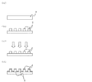
- FIG. 1 It is a figure explaining the measuring method of the optical sensor of this invention. It is a figure explaining the manufacturing method of the optical sensor of this invention. It is a figure explaining the measuring method of the optical sensor of this invention. It is a figure which shows the optical characteristic of the optical sensor A. It is a figure which shows the change of the peak wavelength of the reflected light with respect to the protein density
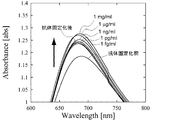
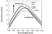
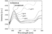
- FIG. It is a figure which shows the optical characteristic of the optical sensor B of this invention. It is a figure which shows the optical characteristic of the optical sensor C of this invention. It is a figure which shows the optical characteristic of the optical sensor D of this invention. It is a figure explaining the measuring method of the optical sensor of this invention. It is a figure explaining the measuring method of the optical sensor of this invention.
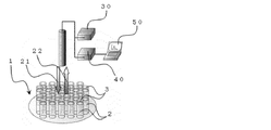
- the optical sensor 1 of the present invention is for detecting a predetermined object, and has a concavo-convex structure 2 in which a predetermined shape is periodically arranged in two dimensions and functions as a photonic crystal. And a metal layer 3 formed on the surface of the concavo-convex structure 2 and capable of exciting localized surface plasmon resonance.
- the concavo-convex structure 2 may be anything as long as it functions as a photonic crystal.
- a hole (see FIG. 1) or a cylinder (see FIG. 10) having a predetermined diameter is two-dimensionally arranged at a predetermined interval.
- a periodically arranged structure can be used.
- a hole or column having a diameter of 50 to 500 nm and periodically arranged in a two-dimensional manner at a pitch of 50 to 1000 nm can be used.
- the material of the concavo-convex structure 2 may be any material as long as it can form a photonic crystal, but preferably an imprint technique (thermal imprinting) capable of forming a uniform concavo-convex structure with a large area with good reproducibility.
- An imprint technique thermal imprinting
- a material to which print, optical imprint, etc. can be applied is preferable.
- cyclic olefin-based resins such as cyclic olefin ring-opening polymerization / hydrogenated product (COP) and cyclic olefin copolymer (COC), acrylic resin, polycarbonate, vinyl ether resin, perfluoroalkoxyalkane (PFA) and polytetrafluoroethylene Fluorine resin such as (PTFE), thermoplastic resin such as polystyrene, polyimide resin, and polyester resin can be used.
- COP cyclic olefin ring-opening polymerization / hydrogenated product
- COC cyclic olefin copolymer
- acrylic resin polycarbonate
- vinyl ether resin vinyl ether resin
- PFA perfluoroalkoxyalkane
- PTFE polytetrafluoroethylene Fluorine resin
- thermoplastic resin such as polystyrene, polyimide resin, and polyester resin
- a resin produced by a polymerization reaction (thermosetting or photocuring) of group-containing compounds can also be used. It is also possible to use the polymerizable reactive group-containing compounds alone for thermal polymerization, and it is also possible to add and use a thermally reactive initiator to improve thermosetting. is there. Furthermore, the concavo-convex structure 2 may be formed by adding a photoreactive initiator and causing the polymerization reaction to proceed by light irradiation.
- Organic peroxides and azo compounds can be preferably used as the heat-reactive radical initiator, and acetophenone derivatives, benzophenone derivatives, benzoin ether derivatives, xanthone derivatives and the like can be preferably used as the photoreactive radical initiator.
- the reactive monomer may be used without a solvent, or may be used after being dissolved in a solvent and desolvated after coating.
- any substrate that does not impair the desired sensor sensitivity can be selected, such as a cyclic olefin resin, a transparent plastic substrate such as an acrylic resin or PET, a quartz substrate, a sapphire substrate, A transparent substrate is particularly preferred.
- the water absorption rate of the resin is preferably 3% or less.
- the heat generation start temperature (oxidation start temperature) of the heat generation peak accompanying oxidation is the glass of the resin.
- the transition temperature is preferably + 35 ° C or higher. This is because in the fine processing by thermal imprinting, particle-like objects on the surface of the resin caused by resin deterioration can be prevented, so that transfer defects and mold release defects of the concavo-convex structure 2 can be greatly reduced.
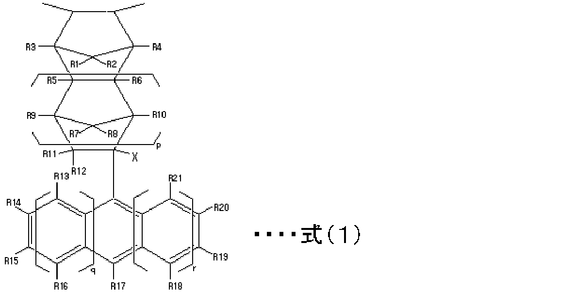
- the thermal imprinting resin is preferably made of a cyclic olefin resin, more preferably a thermal imprinting resin containing at least one repeating unit represented by the formula (1).
- X is a halogen atom or a hydrocarbon group having 1 to 12 carbon atoms.
- X and R21 may be bonded to each other via an alkylene group, etc.
- p, q, r is 0, 1 or 2.
- R1 to R21 are each independently a hydrogen atom, a halogen atom, an aliphatic hydrocarbon group, and an alicyclic hydrocarbon group
- R11 (or R12) and R13 (or R14) may be bonded via an alkylene group having 1 to 5 carbon atoms, or may be bonded via any group, provided that R11 (or R12) and R13 (or R14) and R11 (or R12) is a halogen atom or a hydrocarbon group having 1 to 12 carbon atoms
- R13 (or R14) is a hydrogen atom, halogen An atom, an aliphatic hydrocarbon group, or an alicyclic hydrocarbon group.
- the concavo-convex structure 2 By forming the concavo-convex structure 2 in this way, when the concavo-convex structure 2 is irradiated with light, light having a specific wavelength corresponding to the concavo-convex structure 2 is reflected by the function of the photonic crystal. In addition, if any substance is adsorbed on the concavo-convex structure 2 and the concavo-convex structure 2 is slightly changed, the wavelength and intensity of the reflected light change accordingly. Therefore, a predetermined object to be detected can be detected by the change.
- the concavo-convex structure 2 may be formed of a material that is dissolved or decomposed by an object to be detected.
- the concavo-convex structure 2 when the object to be detected is a polar solvent, the concavo-convex structure 2 is formed by a polar substance that dissolves in this polar solvent, and when the object to be detected is a nonpolar solvent, the nonpolarity that dissolves in this nonpolar solvent. It may be formed by a substance.
- the concavo-convex structure 2 is dissolved or decomposed, but in this case also, the concavo-convex structure 2 is changed. Accordingly, the wavelength and intensity of the reflected light change. Therefore, a predetermined object to be detected can be detected by the change.
- the metal layer 3 is for exciting localized surface plasmon resonance, and is formed in a state of being localized on the surface of the concavo-convex structure 2 described above, for example.
- the metal layer 3 may be formed at least on the bottom of the hole (see FIG. 1), and if it is a column, the metal layer 3 may be formed on the pillar (see FIG. 1). 10).
- the metal used for the metal layer 3 may be any metal that can excite localized surface plasmon resonance, and examples thereof include gold, silver, copper, platinum, and aluminum. These may be used alone or in combination. In addition, an intervening layer of chromium or the like may be provided in consideration of bondability with the material used for the uneven structure 2.
- the thickness of the metal layer 3 is arbitrary, but it is preferably 5 to 200 nm in consideration of sensitivity.
- the metal layer 3 By forming the metal layer 3 in this manner, when the metal layer 3 is irradiated with light, light having a specific wavelength is absorbed by localized surface plasmon resonance. Further, if any substance is adsorbed on the metal layer 3 and there is a slight change in the metal layer 3, the wavelength or intensity of the absorbed light changes accordingly. Therefore, a predetermined object to be detected can be detected by the change.
- the concavo-convex structure 2 and the metal layer 3 may be formed of a material that is dissolved or decomposed by an object to be detected.
- the concavo-convex structure 2 when the object to be detected is a polar solvent, the concavo-convex structure 2 is formed by a polar substance that dissolves in this polar solvent, and when the object to be detected is a nonpolar solvent, the nonpolarity that dissolves in this nonpolar solvent. It may be formed by a substance.
- the concavo-convex structure 2 is dissolved or decomposed, but also in this case, the concavo-convex structure 2 and the metal layer 3 are changed. As a result, the wavelength and intensity of reflected light and transmitted light change accordingly. Therefore, a predetermined object to be detected can be detected by the change.
- the object to be detected can be obtained from two optical characteristics. Double detection is possible, and detection accuracy of an object to be detected can be increased.
- the difference between the peak wavelength of light reflected from the concavo-convex structure 2 and the peak wavelength of light absorbed by the metal layer 3 may be made as small as possible. This is because, when formed in this manner, the change in reflected light as a photonic crystal by the concavo-convex structure 2 and the change in absorbed light as localized surface plasmon resonance by the metal layer 3 overlap, so that the metal layer on the concavo-convex structure 2 This is because, when an object to be detected is attached to 3, the change in the light reflected from or absorbed by the optical sensor 1 becomes large before and after that, and the sensitivity as the optical sensor 1 is improved.
- the basic equation of the two-dimensional photonic crystal is lambda: wavelength of reflected light d: a distance of the holes between theta: angle of incidence n a of the light: average refractive index f: area proportion hole occupies n hole: the refractive index of the hole n medium: the refractive index of the surrounding medium pore From the Bragg equation, It can be expressed as.
- the divergence condition is that the denominator of the polarizability becomes 0, and a resonance phenomenon occurs at this time.
- the resonance frequency of localized surface plasmon resonance generated in a metal layer that is sufficiently smaller than the wavelength of incident light is determined by the dielectric constant ⁇ m ( ⁇ ) of the metal layer and the medium ⁇ 1 around the metal layer. If the size of the metal layer is not negligible compared to the wavelength of the incident light, the resonance frequency can be derived by using Mie's scattering theory, but actually the diameter and shape of the metal layer can also be derived. It is known to depend.
- the size of the metal layer 3 is determined.
- the distance between the holes and the average refractive index may be controlled such that the peak wavelength of the light absorbed by the localized surface plasmon resonance is fixed, and this wavelength is the same as the peak wavelength of the light reflected by the photonic crystal.
- the difference between the peak wavelength of the light reflected from the concavo-convex structure 2 and the peak wavelength of the light absorbed by the metal layer 3 depends on the performance of the light receiving means for receiving reflected light and absorbed light, but is 10 nm or less. Good, preferably 5 nm or less.
- An adsorbing element that specifically adsorbs an object to be detected may be formed on the surface of one or both of the uneven structure 2 and the metal layer 3 described above.
- the material used for the adsorption element any material can be used as long as it can specifically bind an object to be detected and can be fixed to the uneven structure 2 or the metal layer 3.
- an antibody for an antigen an antigen for an antibody, an antigen for an antibody, an anti-hapten antibody for a hapten, a hapten for an anti-hapten antibody, a DNA or PNA that can hybridize to DNA, biotin For avidin or streptavidin, biotin or biotinylated protein for avidin or streptavidin, hormone (eg insulin) for hormone receptor (eg insulin receptor), hormone (eg insulin) Includes hormone receptors (for example, insulin receptor), sugar chains corresponding to lectins, lectins corresponding to sugar chains, and the like.
- the adsorbing element also includes those fragments or subunits having specific binding ability.
- the cell itself can be selected as the adsorbing element, and the detected object in this case may specifically recognize a part of the cell (such as a receptor).
- a to-be-detected object is what can adsorb
- biological materials include antigens, antibodies, receptors, ligands, lectins, sugar chain compounds, RNA, DNA, PNA, and haptens.
- hormones, immunoglobulins, coagulation factors, enzymes, drugs and the like are included.
- Substance names include serum albumin, macroglobulin, ferritin, ⁇ -fetoprotein, CEA, prostate specific antigen (PSA), hepatitis B virus surface antigen (HBsAg), HIV-1P24, and the like.
- the optical sensor of the present invention has a shape and material that can easily apply the nanoimprint technology, even if it has only a function as a photonic crystal without the metal layer 3. Superior to conventional sensors. This is because the nanoimprint technology can process a minute structure precisely and easily, and therefore can provide a sensor with low manufacturing cost and extremely high sensitivity and reliability. In addition, conventional optical sensors have low reproducibility, and errors between manufactured optical sensors are very large. Therefore, it is difficult to compare optical characteristics between different optical sensors. However, since the same optical sensor formed by nanoimprint technology can be mass-produced with high reproducibility, optical characteristics can be compared even between different optical sensors. Therefore, there is also an advantage that simpler detection can be performed by converting the change in the optical characteristics due to the concentration of the object to be detected into a database. Furthermore, it also has significance as an intermediate for producing the optical sensor 1 in which the metal layer 3 is formed.
- the method for manufacturing an optical sensor according to the present invention includes a concavo-convex structure forming step for forming a concavo-convex structure 2 in which a predetermined shape is periodically arranged two-dimensionally and functions as a photonic crystal, and a localized surface plasmon on the surface of the concavo-convex structure 2. And a metal layer forming step for forming the metal layer 3 capable of exciting resonance.
- the concavo-convex structure forming step may be any concavo-convex structure in which a predetermined shape is two-dimensionally accurately and periodically arranged and can function as a photonic crystal. It is better to use printing technology.
- thermoplastic resin 9 When using the thermal imprint technique, first, a film or a substrate made of the thermoplastic resin 9 is prepared, and a desired pattern is formed thereon.
- thermoplastic resin examples include cyclic olefin resins such as cyclic olefin polymers and cyclic olefin copolymers (COC), acrylic resins, polycarbonates, vinyl ether resins, perfluoroalkoxyalkanes (PFA), polytetrafluoroethylene ( Fluorine resin such as PTFE), polyester resin, or the like can be used.
- cyclic olefin resins such as cyclic olefin polymers and cyclic olefin copolymers (COC)
- acrylic resins polycarbonates
- vinyl ether resins vinyl ether resins
- PFA perfluoroalkoxyalkanes
- Fluorine resin such as PTFE
- polyester resin or the like
- the mold 10 formed of a metal such as nickel, ceramics, a carbon material such as glassy carbon, silicon, or the like is heated to a temperature higher than the glass transition temperature of the thermoplastic resin 9.
- the film or substrate made of a thermoplastic resin is pressed (FIG. 2 (a)).
- the thermoplastic resin is cooled to below the glass transition temperature and then released. Thereby, the pattern 10a (inverted pattern of the concavo-convex structure 2) formed on the mold is transferred (FIG. 2B).
- the formation method of the concavo-convex structure 2 is not limited to this, and it can be formed by applying a semiconductor fine processing technique or the like.
- the metal layer forming process may be any process that can be formed on the concavo-convex structure 2 in a state where a metal capable of exciting localized surface plasmon resonance is localized.
- PVD physical vapor deposition
- FOG. 2C concavo-convex structure 2
- CVD chemical vapor deposition method
- electroless plating the thickness of the metal layer 3 is arbitrary, but it is preferably 5 to 200 nm in view of sensitivity.
- an adsorption element when an adsorption element is formed on the concavo-convex structure 2 or the metal layer 3, it is formed using physical adsorption by hydrophobic interaction, chemical bonding to the metal layer 3 by chemicals, or the like. (Adsorption element formation process).
- a housing or a frame may be constructed in a shape that does not impair the sensor performance to form a chip.
- the optical sensor 1 in a state where an object to be detected or the like is not adsorbed is irradiated with the light 21 to obtain information on the optical characteristics of the reflected light 22, particularly the peak wavelength and intensity of the reflected light (see FIG. 1 or FIG. 10).
- Any light source 30 may be used.
- a tungsten / halogen light source, a light emitting diode, an LED, a deuterium lamp, an organic EL, a laser, or the like may be used.
- a multichannel spectroscope, a CCD image sensor, a CMOS sensor, or the like can be used as the light detection means 40 that detects reflected light.
- information processing means 50 such as a computer may be used for processing the acquired information.
- the optical characteristics of the reflected light when the concentration of the object to be detected contained in the sample is changed in advance are detected by the optical sensor 1 and converted into a data base, and the sample is brought into contact with the concavo-convex structure 2.
- the presence / absence or amount of the object to be detected contained in the solution may be detected by comparing the optical characteristics of the light reflected from the optical sensor. In this case, the operation (1) becomes unnecessary.
- the optical sensor 1 may be irradiated with light, and information regarding the optical characteristics of the transmitted light 23 may be used (see FIG. 3 or FIG. 11). In this case, it may be used as follows. (1) First, the optical sensor 1 in a state where an object to be detected or the like is not adsorbed is irradiated with light 21 to acquire information on the optical characteristics of the transmitted light 23, particularly the peak wavelength and intensity of the transmitted light 23. (2) Next, after a sample that may contain an object to be detected is brought into contact with the concavo-convex structure 2 of the optical sensor 1 of the present invention, information on the optical characteristics of the transmitted light 23 is obtained in the same manner. (3) Finally, the optical characteristics of the light transmitted through the optical sensor and the optical characteristics of the light transmitted through the optical sensor after contacting the sample with the concavo-convex structure 2 are included in the solution. The presence or amount of the detected object is detected.
- the optical characteristics of the transmitted light when the concentration or the like of the detection object contained in the sample is changed in advance are detected by the optical sensor 1 and converted into a wrinkle database, and this data and the concavo-convex structure 2 are stored in the sample.
- the optical characteristics of the light transmitted through the optical sensor after contact with the optical sensor the presence / absence or amount of the object to be detected contained in the solution may be detected. In this case, the operation (1) becomes unnecessary.
- a cyclic olefin resin film having a glass transition temperature (Tg) of 163 ° C. made by Nippon Zeon Co., Ltd., trade name: ZEONOR film ZF-16: thickness 100 ⁇ m
- the pattern was transferred to produce an optical sensor A having a concavo-convex structure in which a plurality of holes having a diameter of about 250 nm and a depth of 150 nm were arranged at a pitch of 500 nm.
- Thermal imprinting was performed by the following method. First, a nickel mold preheated to 205 ° C. is pressed against the resin film at a pressure of 2 MPa for 180 seconds. Next, after cooling the nickel mold and the resin film to 100 ° C., the nickel mold is released from the resin film to form a hole-shaped uneven structure. For thermal imprinting, an SCVAX imprinting device (VX) was used.
- VX SCVAX imprinting device
- human chorionic gonadotropin As a protein, human chorionic gonadotropin (hCG), which is a hormone produced during pregnancy, was used and adjusted to a concentration of 1 pg / ml, 10 pg / ml, and 100 pg / ml with ultrapure water. Next, this solution was dropped onto the optical sensor A and allowed to stand at room temperature for 5 minutes, whereby the human chorionic gonadotropin was physically adsorbed onto the concavo-convex structure 2. After standing, cleaning operation was performed with ultrapure water, excess hCG was removed, and the optical properties were evaluated after drying.
- hCG human chorionic gonadotropin
- Optical characteristics are evaluated by vertically emitting white light from a tungsten / halogen light source (Ocean Optics, LS-1) onto the concavo-convex structure 2 of the optical sensor A through a multi-channel fiber (Ocean Optics, r200-7UV / VIS). The reflected light was detected by a multichannel spectrometer (Ocean Optics, USB4000). The optical characteristics were evaluated in the wavelength range of 350 nm to 1000 nm.
- FIG. 5 shows changes in peak wavelength of reflected light with respect to protein concentration
- FIG. 6 shows changes in intensity
- a cyclic olefin resin film having a glass transition temperature (Tg) of 163 ° C. made by Nippon Zeon Co., Ltd., trade name: ZEONOR film ZF-16: thickness 100 ⁇ m
- the pattern is transferred, and a film B having an uneven structure in which holes with a diameter of about 100 nm and a depth of 150 nm are arranged at a pitch of 200 nm, and a plurality of holes with a diameter of about 250 nm and a depth of 150 nm are arranged at a pitch of 500 nm.
- Film C having an uneven structure was prepared.
- Thermal imprinting was performed by the following method. First, a nickel mold preheated to 205 ° C. is pressed against the resin film at a pressure of 2 MPa for 180 seconds. Next, after cooling the nickel mold and the resin film to 100 ° C., the nickel mold is released from the resin film to form a hole-shaped uneven structure. For thermal imprinting, an SCVAX imprinting device (VX) was used.
- VX SCVAX imprinting device
- a metal layer having a thickness of about 30 nm made of gold (Au) was formed on the surface of the concavo-convex structure of film B and film C by vacuum deposition.
- the vacuum deposition was performed by depositing gold (Au) at a deposition rate of 1.0 angstrom or more at a vacuum degree of 1.0 ⁇ 10 ⁇ 3 Pa or less.
- an antibody (adsorbing element) that adsorbs human fibrinogen (detection object) was fixed to the metal layer surface of films B and C, and optical sensor B and optical sensor C were produced.
- the antibody was immobilized by the following method. First, a self-assembled monolayer is formed on the surface of films B and C with DDA (4,4′0Dithiodibutylic acid), and a carboxyl group (—COOH) is introduced. Next, an NHS group is introduced with a 400 mM WSC (Water soluble carbodiimide) / 100 mM NHS mixed solution. An antibody solution prepared with PBS (Phosphate buffered saline, pH 7.4) is added to 100 mg / ml, and the antibody is fixed. Finally, 1M Ethanolamine solution is added to block unreacted NHS groups.
- DDA 4,4′0Dithiodibutylic acid
- Human fibrinogen is adsorbed by adding human ⁇ fibrinogen solutions prepared at concentrations of 1fg / ml, 1pg / ml, 1ng / ml, 1 ⁇ g / ml, and 1mg / ml to optical sensors B and C and let stand for 10 minutes at room temperature.
- human ⁇ fibrinogen solutions prepared at concentrations of 1fg / ml, 1pg / ml, 1ng / ml, 1 ⁇ g / ml, and 1mg / ml to optical sensors B and C and let stand for 10 minutes at room temperature.
- adsorbing it was made to adsorb
- Optical characteristics are evaluated on the concavo-convex structure 2 of the optical sensors B and C using white light from a tungsten / halogen light source (Ocean Optics, LS-1) via a multichannel fiber (Ocean Optics, r200-7UV / VIS).
- the transmitted light was detected by a multi-channel spectrometer (Ocean Optics, USB4000).
- FIG. 7 shows the optical characteristics before and after the adsorption of human fibrinogen on the optical sensor B
- FIG. 8 shows the optical characteristics before and after the adsorption of human fibrinogen on the optical sensor C.
- the absorbances of both optical sensors B and C changed according to the concentration of human fibrinogen.
- the change in absorbance could be observed even when the concentration of human fibrinogen was 1 pg / ml or less.
- a cyclic olefin resin film having a glass transition temperature (Tg) of 163 ° C. made by Nippon Zeon Co., Ltd., trade name: ZEONOR film ZF-16: thickness 100 ⁇ m
- the pattern was transferred to produce a film D having a concavo-convex structure in which a plurality of holes having a diameter of about 200 nm and a depth of 150 nm were arranged at a pitch of 200 nm.
- Thermal imprinting was performed by the following method. First, a nickel mold preheated to 205 ° C. is pressed against the resin film at a pressure of 2 MPa for 180 seconds. Next, after cooling the nickel mold and the resin film to 100 ° C., the nickel mold is released from the resin film to form a hole-shaped uneven structure. For thermal imprinting, an SCVAX imprinting device (VX) was used.
- VX SCVAX imprinting device
- an antibody (adsorbing element) that adsorbs human fibrinogen (object to be detected) was fixed on the surface of the uneven structure of the film D, and an optical sensor D was produced.
- the antibody was immobilized by the following method. First, it is immersed in an anti-human fibrinogen antibody solution (10 ⁇ g / ml) and allowed to stand for 1 hour, and the antibody is fixed to the concavo-convex structure by hydrophobic interaction. This is washed with ultrapure water and dried.
- Human fibrinogen is adsorbed by first preparing a human fibrinogen solution prepared in phosphate buffer (20 mM, pH 7.4) at concentrations of 1 fg / ml, 1 pg / ml, 1 ng / ml, and 1 ⁇ g / ml.
- the type sensor D was immersed for 1 hour.
- a cleaning operation was performed with ultrapure water to remove excess human fibrinogen, and after drying, optical characteristics were evaluated.
- Optical characteristics are evaluated on the concavo-convex structure 2 of the optical sensors B and C using white light from a tungsten / halogen light source (Ocean Optics, LS-1) via a multichannel fiber (Ocean Optics, r200-7UV / VIS).
- the transmitted light was detected by a multi-channel spectrometer (Ocean Optics, USB4000).
- FIG. 9 shows the optical characteristics before and after the adsorption of Human fibrinogen to the optical sensor D.
- the absorbance of the optical sensor D changed according to the concentration of human fibrinogen.
- the change in absorbance could be observed even when the concentration of human fibrinogen was 1 pg / ml or less.
- the optical sensor of the present invention is simple and high even at a minute concentration of 1 pg / ml or less, which is difficult to analyze by the conventional analysis method or requires a large and expensive analyzer. Sensitivity was shown to be detectable.
Landscapes
- Physics & Mathematics (AREA)
- General Physics & Mathematics (AREA)
- Optics & Photonics (AREA)
- Engineering & Computer Science (AREA)
- Chemical & Material Sciences (AREA)
- Nanotechnology (AREA)
- Life Sciences & Earth Sciences (AREA)
- Crystallography & Structural Chemistry (AREA)
- Microelectronics & Electronic Packaging (AREA)
- Health & Medical Sciences (AREA)
- Analytical Chemistry (AREA)
- Biochemistry (AREA)
- General Health & Medical Sciences (AREA)
- Immunology (AREA)
- Pathology (AREA)
- Biophysics (AREA)
- Investigating Or Analysing Materials By Optical Means (AREA)
Abstract
Description
しかしながら、SPR法の場合、共鳴角シフトを検出するために大型の光学系を構築する必要があるとともに、一連の操作が煩雑である。そのためオンサイトでの被検出物のモニタリングに適さない。また、QCM法では、簡便に測定は可能ではあるが、ノイズが大きく、高感度測定には適さない。そしてカンチレバー法ではデバイス作製が非常に困難という点とともに、簡易測定には適さないという問題がある。
2 凹凸構造
3 金属層
21 光
22 反射光
23 透過光
30 光源
40 光検出手段
50 情報処理手段
λ:反射光の波長
d:孔同士の距離
θ:光の入射角
na:平均屈折率
f:孔が占める面積占有率
nhole:孔の屈折率
nmedium:孔の周囲の媒質の屈折率
とすると、ブラッグの式より、


と表すことができる。
rm:金属層の半径
εm(ω):金属層の誘電率
ε1:金属層周囲の媒質
とすると、マクスウェルの方程式より、

で表すことができる。
(1)まず、被検出物等が吸着されていない状態の光学式センサー1に光21を照射し、反射光22の光学特性、特に、反射光のピーク波長や強度に関する情報を取得する(図1又は図10参照)。光源30としてはどのようなものでも良いが、例えば、タングステン・ハロゲン光源や発光ダイオード、LED、重水素ランプ、有機EL、レーザー等を用いれば良い。また、反射光を検出する光検出手段40には、例えば、マルチチャンネル分光器やCCDイメージセンサー、CMOSセンサー等を用いることができる。また、取得した情報の処理には、コンピュータ等の情報処理手段50を用いれば良い。
(2)次に、被検出物が含まれ得る試料を本発明の光学式センサー1の凹凸構造2上に接触させた後、同様に反射光22の光学特性に関する情報を取得する。
(3)最後に、光学式センサーから反射される光の光学特性と、凹凸構造2に試料を接触させた後の光学式センサーから反射される光の光学特性とを比較することにより、溶液中に含まれる被検出物の有無や量を検出する。
(1)まず、被検出物等が吸着されていない状態の光学式センサー1に光21を照射し、透過光23の光学特性、特に、透過光23のピーク波長や強度に関する情報を取得する。
(2)次に、被検出物が含まれ得る試料を本発明の光学式センサー1の凹凸構造2上に接触させた後、同様に透過光23の光学特性に関する情報を取得する。
(3)最後に、光学式センサーを透過した光の光学特性と、凹凸構造2に試料を接触させた後の光学式センサーを透過した光の光学特性とを比較することにより、溶液中に含まれる被検出物の有無や量を検出する。
Claims (16)
- 所定の被検出物を検出するための光学式センサーであって、
所定の形状が二次元的に周期配列されフォトニック結晶として機能する凹凸構造と、
前記凹凸構造の表面に形成され局在表面プラズモン共鳴を励起可能な金属層と、
を具備することを特徴とする光学式センサー。 - 前記凹凸構造から反射される光のピーク波長と前記金属層で吸収される光のピーク波長との差が10nm以下であることを特徴とする請求項1記載の光学式センサー。
- 前記凹凸構造は、50~500nmの範囲内の一定の直径を有する柱又は孔を50~1000nmの範囲内の一定の間隔で二次元的に周期配列したものであることを特徴とする請求項1又は2記載の光学式センサー。
- 前記金属層は、膜厚が5~200nmであることを特徴とする請求項1ないし3のいずれかに記載の光学式センサー。
- 前記金属層は、表面に前記被検出物を吸着する吸着素子を具備することを特徴とする請求項1ないし4のいずれかに記載の光学式センサー。
- 前記凹凸構造は、環状オレフィン系樹脂、アクリル樹脂、ポリカーボネート、ビニルエーテル樹脂、フッ素樹脂、ポリエステル系樹脂のいずれかによって形成されたものであることを特徴とする請求項1ないし5のいずれかに記載の光学式センサー。
- 所定の被検出物を検出するための光学式センサーであって、
所定の形状が二次元的に周期配列されフォトニック結晶として機能する凹凸構造を具備し、当該凹凸構造が環状オレフィン系樹脂、アクリル樹脂、ポリカーボネート、ビニルエーテル樹脂、フッ素樹脂、ポリエステル系樹脂のいずれかから選択された樹脂によって形成されたものであることを特徴とする光学式センサー。 - 前記凹凸構造は、インプリント技術によって形成されたものであることを特徴とする請求項1ないし7のいずれかに記載の光学式センサー。
- 前記凹凸構造は、前記被検出物によって溶解又は分解する材料によって形成されるものであることを特徴とする請求項1ないし8のいずれかに記載の光学式センサー。
- 前記金属層は、前記被検出物によって溶解又は分解する材料によって形成されるものであることを特徴とする請求項1ないし9のいずれかに記載の光学式センサー。
- 前記凹凸構造は、表面に前記被検出物を吸着する吸着素子を具備することを特徴とする請求項1ないし8のいずれかに記載の光学式センサー。
- 所定の被検出物を検出するための光学式センサーの製造方法であって、
所定の形状が二次元的に周期配列されフォトニック結晶として機能する凹凸構造を形成する凹凸構造形成工程と、
前記凹凸構造の表面に局在表面プラズモン共鳴を励起可能な金属層を形成する金属層形成工程と、
を有することを特徴とする光学式センサーの製造方法。 - 前記凹凸構造形成工程は、前記凹凸構造をインプリント技術によって形成することを特徴とする請求項12記載の光学式センサーの製造方法。
- 前記金属層形成工程は、前記金属層を物理気相成長法(PVD)、化学気相成長法(CVD)、メッキ法のいずれかによって形成することを特徴とする請求項12又は13記載の光学式センサーの製造方法。
- 試料中に含まれる被検出物を検出するための検出方法であって、
フォトニック結晶として機能する凹凸構造と、前記凹凸構造の表面に形成され局在表面プラズモン共鳴を励起可能な金属層とを有し、前記凹凸構造から反射される光のピーク波長と前記金属層で吸収される光のピーク波長との差が10nm以下である光学式センサーを用意し、
前記光学式センサーから反射される光の特性と、前記凹凸構造に前記試料を接触させた後の前記光学式センサーから反射される光の特性と、を比較することにより、前記溶液中に含まれる被検出物を検出することを特徴とする検出方法。 - 試料中に含まれる被検出物を検出するための検出方法であって、
フォトニック結晶として機能する凹凸構造と、前記凹凸構造の表面に形成され局在表面プラズモン共鳴を励起可能な金属層とを有し、前記凹凸構造から反射される光のピーク波長と前記金属層で吸収される光のピーク波長との差が10nm以下である光学式センサーを用意し、
種々の濃度の被検出物を含有する試料を前記光学式センサーに接触させて、当該光学式センサーから反射される光の特性を検出して作成したデーターベースを用意し、
前記凹凸構造に前記試料を接触させた後の前記光学式センサーから反射される光の特性と、前記データーベースに蓄積された情報とを比較することにより、前記溶液中に含まれる被検出物を検出することを特徴とする検出方法。
Priority Applications (2)
| Application Number | Priority Date | Filing Date | Title |
|---|---|---|---|
| JP2010533836A JP5488469B2 (ja) | 2008-10-17 | 2009-10-16 | 光学式センサーおよびその製造方法並びに光学式センサーを用いた検出方法 |
| US13/126,343 US20120038926A1 (en) | 2008-10-17 | 2009-10-16 | Optical sensor, method for manufacturing same and detection method using optical sensor |
Applications Claiming Priority (2)
| Application Number | Priority Date | Filing Date | Title |
|---|---|---|---|
| JP2008-269231 | 2008-10-17 | ||
| JP2008269231 | 2008-10-17 |
Publications (1)
| Publication Number | Publication Date |
|---|---|
| WO2010044274A1 true WO2010044274A1 (ja) | 2010-04-22 |
Family
ID=42106444
Family Applications (1)
| Application Number | Title | Priority Date | Filing Date |
|---|---|---|---|
| PCT/JP2009/005415 Ceased WO2010044274A1 (ja) | 2008-10-17 | 2009-10-16 | 光学式センサーおよびその製造方法並びに光学式センサーを用いた検出方法 |
Country Status (3)
| Country | Link |
|---|---|
| US (1) | US20120038926A1 (ja) |
| JP (1) | JP5488469B2 (ja) |
| WO (1) | WO2010044274A1 (ja) |
Cited By (11)
| Publication number | Priority date | Publication date | Assignee | Title |
|---|---|---|---|---|
| WO2013129665A1 (ja) * | 2012-03-01 | 2013-09-06 | 日本精工株式会社 | 標的物質捕捉装置およびそれを備えた標的物質検出装置 |
| WO2013179342A1 (ja) * | 2012-05-30 | 2013-12-05 | 株式会社バイオマーカーサイエンス | バイオチップ |
| JP2014160021A (ja) * | 2013-02-20 | 2014-09-04 | Nsk Ltd | 標的物質捕捉装置およびそれを備えた標的物質検出装置 |
| WO2014168041A1 (ja) * | 2013-04-12 | 2014-10-16 | 日本精工株式会社 | 標的物質捕捉装置 |
| JP2014206463A (ja) * | 2013-04-12 | 2014-10-30 | 日本精工株式会社 | 標的物質捕捉装置 |
| JP2015141144A (ja) * | 2014-01-30 | 2015-08-03 | 国立大学法人 東京大学 | 光学素子 |
| CN109470652A (zh) * | 2018-10-24 | 2019-03-15 | 北京邮电大学 | 基于Fano谐振的椭圆空气孔部分刻蚀型光子晶体传感器 |
| JP2021068821A (ja) * | 2019-10-24 | 2021-04-30 | 国立大学法人東京農工大学 | 熱電変換素子 |
| JP2021177166A (ja) * | 2020-05-04 | 2021-11-11 | ディージー グループ エス ピー エー | バクテリア及び/又はウイルス検出用比色センサー |
| JP2023044017A (ja) * | 2021-09-17 | 2023-03-30 | 公立大学法人大阪 | 検出装置、および、検出方法 |
| KR102961865B1 (ko) * | 2020-05-04 | 2026-05-07 | 디쥐 그룹 에스.피.에이. | 박테리아 및/또는 바이러스를 검출하기 위한 비색 센서 |
Families Citing this family (5)
| Publication number | Priority date | Publication date | Assignee | Title |
|---|---|---|---|---|
| US20130230931A1 (en) * | 2012-03-01 | 2013-09-05 | Nsk Ltd. | Target substance detecting apparatus, and target substance detecting method |
| JP6134975B2 (ja) * | 2013-04-08 | 2017-05-31 | 富士フイルム株式会社 | 測定用デバイス、測定装置および方法 |
| JP2014206471A (ja) * | 2013-04-12 | 2014-10-30 | Scivax株式会社 | 光学式センサー用検出方法 |
| US11067507B2 (en) * | 2017-06-01 | 2021-07-20 | Versitech Limited | Sensors with gradient nanostructures and associated method of use |
| JP7742632B2 (ja) * | 2021-08-23 | 2025-09-22 | 公立大学法人大阪 | 被検出物質の検出キット、検出システムおよび検出方法 |
Citations (3)
| Publication number | Priority date | Publication date | Assignee | Title |
|---|---|---|---|---|
| JP2005016963A (ja) * | 2003-06-23 | 2005-01-20 | Canon Inc | 化学センサ、化学センサ装置 |
| JP2005257458A (ja) * | 2004-03-11 | 2005-09-22 | Sony Corp | 表面プラズモン共鳴装置 |
| JP2008014732A (ja) * | 2006-07-04 | 2008-01-24 | Tohoku Univ | 表面プラズモン共鳴測定装置 |
Family Cites Families (3)
| Publication number | Priority date | Publication date | Assignee | Title |
|---|---|---|---|---|
| JP4906704B2 (ja) * | 2007-02-08 | 2012-03-28 | キヤノン株式会社 | 面発光レーザ、及び面発光レーザを備えた発光装置 |
| US20100279886A1 (en) * | 2007-04-03 | 2010-11-04 | University Of Rochester | Two-dimensional photonic bandgap structures for ultrahigh-sensitivity biosensing |
| DE102007039784A1 (de) * | 2007-08-23 | 2009-02-26 | Clariant International Limited | Anionische wasserlösliche Additive auf Allyl- und Vinyletherbasis |
-
2009
- 2009-10-16 WO PCT/JP2009/005415 patent/WO2010044274A1/ja not_active Ceased
- 2009-10-16 US US13/126,343 patent/US20120038926A1/en not_active Abandoned
- 2009-10-16 JP JP2010533836A patent/JP5488469B2/ja active Active
Patent Citations (3)
| Publication number | Priority date | Publication date | Assignee | Title |
|---|---|---|---|---|
| JP2005016963A (ja) * | 2003-06-23 | 2005-01-20 | Canon Inc | 化学センサ、化学センサ装置 |
| JP2005257458A (ja) * | 2004-03-11 | 2005-09-22 | Sony Corp | 表面プラズモン共鳴装置 |
| JP2008014732A (ja) * | 2006-07-04 | 2008-01-24 | Tohoku Univ | 表面プラズモン共鳴測定装置 |
Non-Patent Citations (3)
| Title |
|---|
| OSAMU SATO ET AL.: "Kin Nano Ryushi Coating Photonic Kessho ni yoru Hyomen Plasmon Sensor", JAPANESE JOURNAL OF OPTICS, vol. 34, no. 10, 2005, pages 530 - 532 * |
| REO ABE ET AL.: "Denshisen Lithography o Mochiita Nano Kozo no Keisei to Kyokuzai Hyomen Plasmon Kyomei no Reiki", THE CHEMICAL SOCIETY OF JAPAN DAI 86 SHUNKI NENKAI (2006) KOEN YOKOSHU II, 30 March 2006 (2006-03-30), pages 945 * |
| TAKUHO SHA ET AL.: "2-Jigen Kinzoku Photonic Kessho o Mochiita Terahertz Hyomen Plasmon Sensor", THE JAPAN SOCIETY OF APPLIED PHYSICS 2004 NEN SHUKI DAI 65 KAI EXTENDED ABSTRACTS, 2004, pages 982 * |
Cited By (16)
| Publication number | Priority date | Publication date | Assignee | Title |
|---|---|---|---|---|
| WO2013129665A1 (ja) * | 2012-03-01 | 2013-09-06 | 日本精工株式会社 | 標的物質捕捉装置およびそれを備えた標的物質検出装置 |
| WO2013179342A1 (ja) * | 2012-05-30 | 2013-12-05 | 株式会社バイオマーカーサイエンス | バイオチップ |
| JPWO2013179342A1 (ja) * | 2012-05-30 | 2016-01-14 | 株式会社バイオマーカーサイエンス | バイオチップ |
| JP2014160021A (ja) * | 2013-02-20 | 2014-09-04 | Nsk Ltd | 標的物質捕捉装置およびそれを備えた標的物質検出装置 |
| US10379111B2 (en) | 2013-04-12 | 2019-08-13 | Nsk Ltd. | Target substance capturing device |
| WO2014168041A1 (ja) * | 2013-04-12 | 2014-10-16 | 日本精工株式会社 | 標的物質捕捉装置 |
| JP2014206463A (ja) * | 2013-04-12 | 2014-10-30 | 日本精工株式会社 | 標的物質捕捉装置 |
| JP5900615B2 (ja) * | 2013-04-12 | 2016-04-06 | 日本精工株式会社 | 標的物質捕捉装置 |
| JP2015141144A (ja) * | 2014-01-30 | 2015-08-03 | 国立大学法人 東京大学 | 光学素子 |
| CN109470652A (zh) * | 2018-10-24 | 2019-03-15 | 北京邮电大学 | 基于Fano谐振的椭圆空气孔部分刻蚀型光子晶体传感器 |
| JP2021068821A (ja) * | 2019-10-24 | 2021-04-30 | 国立大学法人東京農工大学 | 熱電変換素子 |
| JP7392972B2 (ja) | 2019-10-24 | 2023-12-06 | 国立大学法人東京農工大学 | 熱電変換素子 |
| JP2021177166A (ja) * | 2020-05-04 | 2021-11-11 | ディージー グループ エス ピー エー | バクテリア及び/又はウイルス検出用比色センサー |
| JP7786881B2 (ja) | 2020-05-04 | 2025-12-16 | ディージー グループ エス ピー エー | バクテリア及び/又はウイルス検出用比色センサー |
| KR102961865B1 (ko) * | 2020-05-04 | 2026-05-07 | 디쥐 그룹 에스.피.에이. | 박테리아 및/또는 바이러스를 검출하기 위한 비색 센서 |
| JP2023044017A (ja) * | 2021-09-17 | 2023-03-30 | 公立大学法人大阪 | 検出装置、および、検出方法 |
Also Published As
| Publication number | Publication date |
|---|---|
| JP5488469B2 (ja) | 2014-05-14 |
| JPWO2010044274A1 (ja) | 2012-03-15 |
| US20120038926A1 (en) | 2012-02-16 |
Similar Documents
| Publication | Publication Date | Title |
|---|---|---|
| JP5488469B2 (ja) | 光学式センサーおよびその製造方法並びに光学式センサーを用いた検出方法 | |
| Oliverio et al. | Chemical functionalization of plasmonic surface biosensors: a tutorial review on issues, strategies, and costs | |
| JP2010145408A (ja) | バイオチップ及び生体物質検出装置 | |
| JP5720248B2 (ja) | 表面プラズモンおよび蛍光共鳴エネルギー転移を利用した免疫アッセイ | |
| US7403287B2 (en) | Sensing element used in sensing device for sensing target substance in specimen by using plasmon resonance | |
| KR20090128528A (ko) | 바이오센서를 위한 교정 및 정규화 방법 | |
| JP2005181296A (ja) | 局在化表面プラズモンセンサ、センシング装置およびセンシング方法 | |
| WO2002056012A1 (en) | Fluorescent analysis element with the use of metallic nanowell and process for producing the same | |
| Chen et al. | Near-infrared surface plasmon resonance sensor with a graphene-gold surface architecture for ultra-sensitive biodetection | |
| Krizkova et al. | Nanotechnologies in protein microarrays | |
| US7915053B2 (en) | Substrate for target substance detecting device, target substance detecting device, target substance detecting apparatus and method using the same, and kit therefor | |
| JP2006250668A (ja) | 非標識バイオチップ | |
| CN101825629B (zh) | 波导耦合金属光子晶体生物传感器及其检测方法 | |
| Kashyap et al. | Multiple protein‐patterned surface plasmon resonance biochip for the detection of human immunoglobulin‐G | |
| Chen et al. | Novel Multifunctional Meta‐Surface Plasmon Resonance Chip Microplate for High‐Throughput Molecular Screening | |
| US20150204865A1 (en) | Sensing method | |
| Rastogi et al. | Quantifying analyte surface densities and their distribution with respect to electromagnetic hot spots in plasmon-enhanced spectroscopic biosensors | |
| CN102246042B (zh) | 用于检测流体中的靶元素的感测器件 | |
| JP4580291B2 (ja) | バイオセンサーを用いた測定方法 | |
| US7829349B2 (en) | Base carrier for detecting target substance, element for detecting target substance, method for detecting target substance using the element, and kit for detecting target substance | |
| EP1969352A2 (en) | Method for increasing signal intensity in an optical waveguide sensor | |
| WO2011065398A1 (ja) | 光学式センサー及びその製造方法 | |
| Linman et al. | Etched glass microarrays with differential resonance for enhanced contrast and sensitivity of surface plasmon resonance imaging analysis | |
| TWI316603B (en) | Method for immunoassays based on infrared reflection absorption spectroscopy | |
| WO2009150583A1 (en) | Diagnostic device |
Legal Events
| Date | Code | Title | Description |
|---|---|---|---|
| 121 | Ep: the epo has been informed by wipo that ep was designated in this application |
Ref document number: 09820452 Country of ref document: EP Kind code of ref document: A1 |
|
| WWE | Wipo information: entry into national phase |
Ref document number: 2010533836 Country of ref document: JP |
|
| NENP | Non-entry into the national phase |
Ref country code: DE |
|
| WWE | Wipo information: entry into national phase |
Ref document number: 13126343 Country of ref document: US |
|
| 122 | Ep: pct application non-entry in european phase |
Ref document number: 09820452 Country of ref document: EP Kind code of ref document: A1 |