WO2010044193A1 - 試料分析方法 - Google Patents
試料分析方法 Download PDFInfo
- Publication number
- WO2010044193A1 WO2010044193A1 PCT/JP2009/004735 JP2009004735W WO2010044193A1 WO 2010044193 A1 WO2010044193 A1 WO 2010044193A1 JP 2009004735 W JP2009004735 W JP 2009004735W WO 2010044193 A1 WO2010044193 A1 WO 2010044193A1
- Authority
- WO
- WIPO (PCT)
- Prior art keywords
- sample
- wave
- interface
- analysis method
- incident
- Prior art date
Links
- 238000012284 sample analysis method Methods 0.000 title claims abstract description 24
- 230000035699 permeability Effects 0.000 claims abstract description 5
- 238000004458 analytical method Methods 0.000 claims description 8
- 230000000704 physical effect Effects 0.000 abstract description 13
- 239000000203 mixture Substances 0.000 abstract description 8
- 239000000523 sample Substances 0.000 description 188
- 239000012528 membrane Substances 0.000 description 33
- 238000000034 method Methods 0.000 description 29
- YBJHBAHKTGYVGT-ZKWXMUAHSA-N (+)-Biotin Chemical compound N1C(=O)N[C@@H]2[C@H](CCCCC(=O)O)SC[C@@H]21 YBJHBAHKTGYVGT-ZKWXMUAHSA-N 0.000 description 24
- 238000005259 measurement Methods 0.000 description 22
- 230000003287 optical effect Effects 0.000 description 19
- 238000001328 terahertz time-domain spectroscopy Methods 0.000 description 18
- 238000001514 detection method Methods 0.000 description 14
- 238000010521 absorption reaction Methods 0.000 description 13
- 238000010586 diagram Methods 0.000 description 13
- 229960002685 biotin Drugs 0.000 description 12
- 235000020958 biotin Nutrition 0.000 description 12
- 239000011616 biotin Substances 0.000 description 12
- 238000005102 attenuated total reflection Methods 0.000 description 11
- 108010090804 Streptavidin Proteins 0.000 description 10
- 239000000463 material Substances 0.000 description 10
- 230000001902 propagating effect Effects 0.000 description 9
- 108090000623 proteins and genes Proteins 0.000 description 8
- 102000004169 proteins and genes Human genes 0.000 description 8
- 150000003384 small molecules Chemical class 0.000 description 8
- 239000000126 substance Substances 0.000 description 7
- 239000000758 substrate Substances 0.000 description 7
- 235000000346 sugar Nutrition 0.000 description 7
- 238000002834 transmittance Methods 0.000 description 7
- 102000004856 Lectins Human genes 0.000 description 6
- 108090001090 Lectins Proteins 0.000 description 6
- 239000002202 Polyethylene glycol Substances 0.000 description 6
- 230000005540 biological transmission Effects 0.000 description 6
- 229920001222 biopolymer Polymers 0.000 description 6
- 238000003384 imaging method Methods 0.000 description 6
- 239000002523 lectin Substances 0.000 description 6
- 229920001223 polyethylene glycol Polymers 0.000 description 6
- 239000010409 thin film Substances 0.000 description 6
- XUIMIQQOPSSXEZ-UHFFFAOYSA-N Silicon Chemical compound [Si] XUIMIQQOPSSXEZ-UHFFFAOYSA-N 0.000 description 5
- 230000002209 hydrophobic effect Effects 0.000 description 5
- 229910052710 silicon Inorganic materials 0.000 description 5
- 239000010703 silicon Substances 0.000 description 5
- GUBGYTABKSRVRQ-QKKXKWKRSA-N Lactose Natural products OC[C@H]1O[C@@H](O[C@H]2[C@H](O)[C@@H](O)C(O)O[C@@H]2CO)[C@H](O)[C@@H](O)[C@H]1O GUBGYTABKSRVRQ-QKKXKWKRSA-N 0.000 description 4
- 239000004698 Polyethylene Substances 0.000 description 4
- 230000000052 comparative effect Effects 0.000 description 4
- 230000005684 electric field Effects 0.000 description 4
- 239000010408 film Substances 0.000 description 4
- 239000008101 lactose Substances 0.000 description 4
- -1 polyethylene Polymers 0.000 description 4
- 229920000573 polyethylene Polymers 0.000 description 4
- 238000000411 transmission spectrum Methods 0.000 description 4
- GUBGYTABKSRVRQ-XLOQQCSPSA-N Alpha-Lactose Chemical compound O[C@@H]1[C@@H](O)[C@@H](O)[C@@H](CO)O[C@H]1O[C@@H]1[C@@H](CO)O[C@H](O)[C@H](O)[C@H]1O GUBGYTABKSRVRQ-XLOQQCSPSA-N 0.000 description 3
- 229910001218 Gallium arsenide Inorganic materials 0.000 description 3
- 239000002033 PVDF binder Substances 0.000 description 3
- 230000008901 benefit Effects 0.000 description 3
- 230000008859 change Effects 0.000 description 3
- 238000002073 fluorescence micrograph Methods 0.000 description 3
- 230000003993 interaction Effects 0.000 description 3
- 239000002184 metal Substances 0.000 description 3
- 229920002981 polyvinylidene fluoride Polymers 0.000 description 3
- 238000001228 spectrum Methods 0.000 description 3
- 238000005406 washing Methods 0.000 description 3
- IJGRMHOSHXDMSA-UHFFFAOYSA-N Atomic nitrogen Chemical compound N#N IJGRMHOSHXDMSA-UHFFFAOYSA-N 0.000 description 2
- 150000001720 carbohydrates Chemical class 0.000 description 2
- 210000004027 cell Anatomy 0.000 description 2
- 238000006243 chemical reaction Methods 0.000 description 2
- 230000000694 effects Effects 0.000 description 2
- 238000001962 electrophoresis Methods 0.000 description 2
- 238000001917 fluorescence detection Methods 0.000 description 2
- 239000007850 fluorescent dye Substances 0.000 description 2
- 229930182830 galactose Natural products 0.000 description 2
- 239000012535 impurity Substances 0.000 description 2
- 230000001678 irradiating effect Effects 0.000 description 2
- 238000012545 processing Methods 0.000 description 2
- 238000012216 screening Methods 0.000 description 2
- 238000001179 sorption measurement Methods 0.000 description 2
- 239000013076 target substance Substances 0.000 description 2
- 150000004044 tetrasaccharides Chemical class 0.000 description 2
- 239000012099 Alexa Fluor family Substances 0.000 description 1
- 102000003886 Glycoproteins Human genes 0.000 description 1
- 108090000288 Glycoproteins Proteins 0.000 description 1
- 239000000020 Nitrocellulose Substances 0.000 description 1
- 101710100170 Unknown protein Proteins 0.000 description 1
- 241000700605 Viruses Species 0.000 description 1
- 238000002835 absorbance Methods 0.000 description 1
- 238000000862 absorption spectrum Methods 0.000 description 1
- 230000002776 aggregation Effects 0.000 description 1
- 238000004220 aggregation Methods 0.000 description 1
- 239000000427 antigen Substances 0.000 description 1
- 102000036639 antigens Human genes 0.000 description 1
- 108091007433 antigens Proteins 0.000 description 1
- 230000000903 blocking effect Effects 0.000 description 1
- 239000000969 carrier Substances 0.000 description 1
- 230000010261 cell growth Effects 0.000 description 1
- 239000000919 ceramic Substances 0.000 description 1
- 229910010293 ceramic material Inorganic materials 0.000 description 1
- 150000001875 compounds Chemical class 0.000 description 1
- 238000007796 conventional method Methods 0.000 description 1
- 239000013078 crystal Substances 0.000 description 1
- 230000007423 decrease Effects 0.000 description 1
- 238000007876 drug discovery Methods 0.000 description 1
- 238000001035 drying Methods 0.000 description 1
- 238000005530 etching Methods 0.000 description 1
- 230000001747 exhibiting effect Effects 0.000 description 1
- 238000002795 fluorescence method Methods 0.000 description 1
- 238000001215 fluorescent labelling Methods 0.000 description 1
- 150000002256 galaktoses Chemical class 0.000 description 1
- 230000003100 immobilizing effect Effects 0.000 description 1
- 230000036737 immune function Effects 0.000 description 1
- 208000015181 infectious disease Diseases 0.000 description 1
- 238000012844 infrared spectroscopy analysis Methods 0.000 description 1
- 150000002632 lipids Chemical class 0.000 description 1
- 239000007788 liquid Substances 0.000 description 1
- 238000000691 measurement method Methods 0.000 description 1
- 125000002496 methyl group Chemical group [H]C([H])([H])* 0.000 description 1
- 238000001471 micro-filtration Methods 0.000 description 1
- 229920001220 nitrocellulos Polymers 0.000 description 1
- 229910052757 nitrogen Inorganic materials 0.000 description 1
- 239000012466 permeate Substances 0.000 description 1
- 229920003023 plastic Polymers 0.000 description 1
- 239000004033 plastic Substances 0.000 description 1
- 229920006254 polymer film Polymers 0.000 description 1
- 230000008569 process Effects 0.000 description 1
- 238000003672 processing method Methods 0.000 description 1
- 230000000644 propagated effect Effects 0.000 description 1
- 238000010926 purge Methods 0.000 description 1
- 238000004445 quantitative analysis Methods 0.000 description 1
- 230000009257 reactivity Effects 0.000 description 1
- 238000005070 sampling Methods 0.000 description 1
- 238000005245 sintering Methods 0.000 description 1
- 235000020183 skimmed milk Nutrition 0.000 description 1
- 238000012916 structural analysis Methods 0.000 description 1
- 150000008163 sugars Chemical class 0.000 description 1
- 238000012360 testing method Methods 0.000 description 1
- 238000012546 transfer Methods 0.000 description 1
- XLYOFNOQVPJJNP-UHFFFAOYSA-N water Chemical compound O XLYOFNOQVPJJNP-UHFFFAOYSA-N 0.000 description 1
- 238000012982 x-ray structure analysis Methods 0.000 description 1
Images


Classifications
-
- G—PHYSICS
- G01—MEASURING; TESTING
- G01N—INVESTIGATING OR ANALYSING MATERIALS BY DETERMINING THEIR CHEMICAL OR PHYSICAL PROPERTIES
- G01N21/00—Investigating or analysing materials by the use of optical means, i.e. using sub-millimetre waves, infrared, visible or ultraviolet light
- G01N21/17—Systems in which incident light is modified in accordance with the properties of the material investigated
- G01N21/25—Colour; Spectral properties, i.e. comparison of effect of material on the light at two or more different wavelengths or wavelength bands
- G01N21/31—Investigating relative effect of material at wavelengths characteristic of specific elements or molecules, e.g. atomic absorption spectrometry
- G01N21/35—Investigating relative effect of material at wavelengths characteristic of specific elements or molecules, e.g. atomic absorption spectrometry using infrared light
- G01N21/3581—Investigating relative effect of material at wavelengths characteristic of specific elements or molecules, e.g. atomic absorption spectrometry using infrared light using far infrared light; using Terahertz radiation
-
- G—PHYSICS
- G01—MEASURING; TESTING
- G01N—INVESTIGATING OR ANALYSING MATERIALS BY DETERMINING THEIR CHEMICAL OR PHYSICAL PROPERTIES
- G01N21/00—Investigating or analysing materials by the use of optical means, i.e. using sub-millimetre waves, infrared, visible or ultraviolet light
- G01N21/17—Systems in which incident light is modified in accordance with the properties of the material investigated
- G01N21/25—Colour; Spectral properties, i.e. comparison of effect of material on the light at two or more different wavelengths or wavelength bands
- G01N21/31—Investigating relative effect of material at wavelengths characteristic of specific elements or molecules, e.g. atomic absorption spectrometry
- G01N21/35—Investigating relative effect of material at wavelengths characteristic of specific elements or molecules, e.g. atomic absorption spectrometry using infrared light
- G01N21/3563—Investigating relative effect of material at wavelengths characteristic of specific elements or molecules, e.g. atomic absorption spectrometry using infrared light for analysing solids; Preparation of samples therefor
Definitions
- the present invention relates to a technique for analyzing a sample using terahertz waves.
- a terahertz wave refers to an electromagnetic wave having a frequency of 20 GHz to 120 THz. Examples of analysis include measuring physical properties and dimensions of the sample itself, and measuring the amount of biopolymer attached to the sample.
- a measurement result corresponding to the physical property of the sample is obtained. For example, if a sample is irradiated with terahertz waves of different wavelengths, the terahertz wave of a specific wavelength is absorbed by the electromagnetic wave absorption of the sample, so the frequency characteristic of the terahertz wave transmittance is a unique waveform corresponding to the physical properties of the sample Appears as
- THz-TDS terahertz time domain spectroscopy
- Example 2 of Patent Document 1 THz-TDS by a reflective optical system is shown.
- the terahertz wave emitted from the terahertz wave generator is focused and irradiated on the sample through a parabolic mirror, and then the terahertz wave reflected on the sample is reflected using the parabolic mirror. Condensed on the detector.
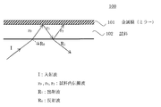
- FIG. 11 was created by the applicant based on the description in Patent Document 1.
- the conventional sample holder 100 includes a sample 102 to be measured and a metal film 101 in contact with the sample 102.
- the metal film 101 is a mirror that reflects almost 100% of the terahertz wave.
- the sample 102 In order to measure the transmittance of the sample 102 with respect to the terahertz wave, the sample 102 is irradiated with the terahertz wave.
- the terahertz wave propagation path in the sample at that time will be described with reference to FIG.
- an irradiation wave I that is a terahertz wave is incident on the sample 102.
- a part of the irradiation wave I becomes a reflected wave R 0 that directly hits and reflects the sample 102, and the other part becomes an in-sample propagation wave r 0 that passes through the sample 102.
- the reflected wave R 0 and the propagation wave r 0 in the sample are refracted due to the difference in permittivity between the atmosphere and the sample 102.
- Samples in propagating wave r 0 is reflected by the metal film 101, the sample in the propagating wave r 1, and the further surface in reflected sample the propagating wave r 2 next to the part of the sample 102 air samples in propagating wave r 1 The remaining part passes through the interface and is emitted to become an outgoing wave R 1 .
- the magnitudes of the amplitudes of the reflected wave R 0 and the outgoing wave R 1 are obtained on the time axis, and Fourier transform is performed to obtain the composition, physical properties, and mass of the sample 102.
- This is the conventional THz-TDS.
- the terahertz wave is not sufficiently absorbed in the sample, and the difference in amplitude between the reflected wave R 0 and the output wave R 1 does not change between when the sample is present and when the sample is present, and sufficient analysis of the sample 102 is performed.
- the transmission path of the terahertz wave itself is shortened, and a situation where electromagnetic wave absorption is not sufficiently performed occurs.
- the electromagnetic wave is not sufficiently absorbed, and it is impossible to measure the minute amount of 1 mg or less by the conventional method.
- the problem to be solved by the present invention is to accurately measure the composition, physical properties, mass, and dimensions of a micro sample, a micro sample, or a thin layer sample.
- the sample analysis method is a sample analysis method for analyzing a sample that is permeable to terahertz waves, and a reflecting member is provided in contact with the first main surface side of the sample.
- An incident member is provided in contact with the second main surface side of the first member, and the sample is irradiated with terahertz waves from the outside of the incident member toward the sample, and the second main surface side is irradiated with a terahertz wave.
- the sample is analyzed using an interference wave generated by a single-surface reflected wave and a second-surface reflected wave at the interface between the second main surface of the sample and the incident member.
- a terahertz wave refers to an electromagnetic wave having a frequency of 20 GHz to 120 THz.
- the interface between the first main surface of the sample and the reflecting member and the interface between the second main surface of the sample and the incident member are parallel.
- the interference wave includes an outgoing wave emitted from the first surface reflected wave through the sample and the incident member, and an incident member from the second surface reflected wave. And an outgoing wave that has passed through and emitted.
- the interference wave is in an interface between the first main surface of the sample and the reflecting member, and an interface between the second main surface of the sample and the incident member.
- a terahertz wave is formed from multiple reflected waves that are reflected multiple times. Multiple reflected waves are reflected waves that are reflected multiple times at the interface between the sample and the reflecting member and at the interface between the sample and the incident member in the process from irradiating the sample with the terahertz wave until it is emitted.
- the refractive index of the reflecting member is larger than the refractive index of the sample
- the refractive index of the incident member is larger than the refractive index of the sample
- the refractive index of the incident member is the incident light. It is larger than the refractive index of the atmosphere existing outside the member.
- a terahertz wave reflection suppressing layer is provided in contact with the outside of the incident member.
- the sample analysis method is a sample analysis method when the sample is formed of a plurality of layers having different dielectric constants, and is an analysis target of the plurality of layers of the sample.
- the layer is brought into contact with the reflective member and the sample is analyzed.
- a sample analysis method is a sample analysis method for analyzing a sample having permeability to terahertz waves, and a reflective member is applied to the first main surface side of the sample.
- An entrance member is provided in contact with the second main surface side of the sample, and a terahertz wave is irradiated from the outside of the entrance member toward the sample, and the first main surface of the sample and the reflection are irradiated.
- the outgoing wave finally emitted to the outside means a terahertz wave that has been emitted to the outside after being propagated through the sample or the incident member, whether once or plural times. .
- sample analysis method of the present invention it is possible to accurately measure the composition, physical properties, mass, and dimensions of a minute sample, a minute sample, or a thin layer sample.
- FIG. 1 is a diagram illustrating a sample holding unit and a terahertz wave propagation path in the sample holding unit in the embodiment.
- FIG. 2 is a diagram illustrating the entire THz-TDS imaging apparatus according to the first embodiment.
- FIG. 3 is a diagram illustrating a specific structure of the sample holder in the first embodiment.
- FIG. 4A is a diagram showing a time waveform by THz-TDS in Example 1
- FIG. 4B is a diagram showing a terahertz wave propagation path in the sample holding unit and the sample holding unit in Example 1. It is.
- FIG. 5 is a diagram illustrating frequency characteristics of transmittance according to the first embodiment.
- FIG. 6A is a diagram illustrating the sample holding unit 40 of the present embodiment, and FIG.
- FIG. 6B is an enlarged view of a portion A in FIG.
- FIG. 7 is a view showing a sample holder in the third embodiment.
- FIG. 8 is a schematic diagram of a biotin membrane array in Example 4 and a fluorescence detection image as a comparative example.
- FIG. 9 is a detection image of streptavidin on the biotin membrane array in Example 4.
- FIG. 10 is a detection image of lectins on the sugar chain membrane array in Example 5.
- FIG. 11 is a diagram for explaining a sample holder and a terahertz wave propagation path in a conventional THz-TDS.
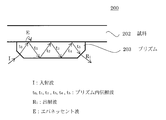
- FIG. 12 is a diagram showing a sample holder and a terahertz propagation path by the ATR method as a comparative example.
- the point that the present invention greatly differs from the prior art will be mainly described.
- the difference from the prior art is the transmission path of the terahertz wave in the sample holder 10 and the sample holder.
- the terahertz light source, optical system, data processing method, and the like will be specifically described in the embodiments.
- the sample holder 10 of this embodiment includes a sample 12 to be measured, a reflecting member 11 that is in contact with one main surface of the sample 12, and an incident that is in contact with the other main surface of the sample 12. It is constituted by the member 13.
- the reflecting member 11 is a mirror having a refractive index larger than that of the sample 12 and reflecting almost 100% of the terahertz wave.
- a member having a negative refractive index such as a metamaterial can be used.
- the incident member 13 is made of a material having a refractive index different from that of the sample 12 and having a refractive index larger than that of the atmosphere. More preferably, the refractive index of the incident member 13 should be larger than the refractive index of the sample 12.
- the material of the incident member 13 is high resistance silicon (Si) or translucent ceramic. This is because the multiple reflection described later can be used effectively.
- the sample 12 is a material having permeability and absorption with respect to terahertz waves.
- the boundary between the reflecting member 11 and the sample 12 is called a first interface 21
- the boundary between the sample 12 and the incident member 13 is called a second interface 22
- the boundary between the incident member 13 and the atmosphere is Called the third interface 23.
- the reflected wave generated at the first interface 21 is called a first surface reflected wave
- the reflected wave generated at the second interface 22 is called a second surface reflected wave
- the reflected wave generated at the third interface 23 is called a third surface. This is called a reflected wave.
- the present invention is characterized in that the sample 12 is analyzed using an interference wave generated by the first surface reflected wave generated at the first interface 21 and the second surface reflected wave generated at the second interface 22. . This will be described below.
- a terahertz wave is irradiated from the outside (atmosphere side) of the incident member 13 toward the sample holding unit 10.
- This irradiation wave I passes through the third interface 23 and becomes a propagation wave t 0 within the incident member.
- refraction occurs in the terahertz wave due to the difference in permittivity between the atmosphere and the incident member 13.
- a part of the propagation wave t 0 within the incident member is incident on the sample 12, and the remaining part is reflected by the second interface 22 to become a propagation wave t 1 (reflection wave) within the incident member.
- a part of the propagation wave t 1 in the incident member is reflected by the third interface 23 to become a propagation wave t 2 (reflection wave) in the incident member, and the remaining part passes through the third interface and is emitted as the outgoing wave R 1. Is done.
- the propagation wave incident on the sample 12 becomes the propagation wave r 0 in the sample and propagates in the sample with a predetermined angle.
- the predetermined angle is determined by the difference in dielectric constant between the incident member 13 and the sample 12.
- the intra-sample propagation wave r 0 is reflected by the first interface 21 and becomes the intra-sample propagation wave r 1 (reflection wave).
- a part of the propagation wave r 1 in the sample reflects the second interface 22, but the remaining part passes through the second interface 22 and further passes through the third interface 23 to be emitted as an outgoing wave R 2. Is done.
- the wave reflected without passing through the third interface 23 becomes the propagation wave r 1 t 2 (reflection wave) in the incident member.
- Propagating waves from the specimen within the propagating wave r 1 and reflected by the second surface 22 is the sample within the propagating wave r 2. After the sample within the propagating wave r 2 is reflected by the first interface 21, some further part passes through the second interface 22 is emitted through the third interface 23, the other the output wave R 3 become.
- the composition, physical properties, mass, and dimensions of the sample 12 can be obtained by obtaining the magnitude of the amplitude of the interference wave formed by the outgoing wave R 1 and the outgoing wave R 2 at this time on the time axis and performing Fourier transform. . Further, the magnitude of the amplitude of the interference wave formed from the outgoing wave R 1 , the outgoing wave R 2, and the outgoing wave R 3 can be obtained on the time axis and Fourier transformed. Furthermore, the amplitude of the interference wave formed by multiple reflection at the first interface 21, the second interface 22, and the third interface 23 is obtained on the time axis, and is subjected to Fourier transform, thereby making the composition of the sample 12 more accurate. , Physical properties, mass, dimensions can be obtained.
- the present invention has an advantage that the angle of the reflected wave from the second interface 22 can be measured stably since the incident member 13 having a smooth surface is provided on the sample holder 10 as shown in FIG. Furthermore, in the present invention, since the sample holding unit 10 is provided with the surface-smooth incident member 13 and the distance between the second interface 22 and the detection element 36 is constant, the sample is scanned in the in-plane direction to perform multipoint measurement. There is an advantage that the reflected wave from the second interface 22 can be measured on the same time basis. Therefore, the physical properties of the sample 12 can be accurately measured.
- the incident surface 13 having a smooth surface is provided in the sample holder 10 and the multiple reflection of the terahertz wave at the second interface and the first interface is actively used, so that the transmission path of the terahertz wave is substantially reduced. This makes it possible to measure even very small samples.
- the sample surface touches the atmosphere before the sample 102 is placed in the measuring apparatus, and impurities in the atmosphere adhere to the sample during that time, preventing accurate measurement.
- the sample 12 is sandwiched between the reflecting member 11 and the incident member 13, so that the sample 12 is not directly in contact with the atmosphere, and the problem that impurities adhere later can be solved.
- an ATR (Attenuated Total Reflection) method is cited as a comparative example, and the comparative example is compared with the present invention.
- the ATR method is an infrared spectroscopic analysis method using infrared light. As shown in FIG. 12, the sample 202 and a Si (silicon) prism 203 having a higher refractive index are brought into contact with each other, the incident angle of the irradiation wave I that is infrared light is adjusted, and total reflection occurs inside the prism. In this way, the outgoing wave R 1 is measured.
- the infrared light slightly enters the sample 202 by a predetermined depth and then reflects, so that an infrared absorption spectrum on the surface of the sample 202 is obtained.
- structural analysis and qualitative quantitative analysis of the sample 202 can be performed.
- the characteristic of the ATR method is that the evanescent wave E that enters the sample 202 by a predetermined depth is used.
- the number of multiple reflections determined by the length and thickness of the prism 203 and the incident angle of the irradiation wave I emitted from the light source is the number of times the sample 202 is sampled. .
- the present invention is different from the ATR method in the following points.
- the present invention and the ATR method are the same in that multiple reflections of terahertz waves are used.
- the ATR method causes multiple reflections on the outer surface of the sample 202 and uses multiple reflections occurring in the prism 203.
- the principle of the present invention is different in that the present invention also uses the multiple reflection occurring in the sample 12.
- the present invention using electromagnetic wave absorption in a sample is more susceptible to electromagnetic wave absorption than the ATR method using electromagnetic wave absorption by the sample surface, and is suitable for detecting a minute amount of the sample 12.
- the ATR method is a multiple reflection within the incident member (inside the prism) and does not utilize the multiple reflection within the sample, so it is not suitable for measuring a sample that transmits a terahertz wave.
- the present invention is a measurement method suitable for the sample 12 that transmits a terahertz wave, and is completely different from the ATR method in that multiple reflection in the sample is used.
- FIG. 2 shows an imaging system 30 using terahertz time domain spectroscopy (THz-TDS).
- the imaging system 30 is configured such that an XY stage 34 for driving a sample is disposed in the THz-TDS optical path, and an image can be acquired by raster scanning of the sample 12, and a transmittance image and absorbance at each frequency are obtained. An image can be obtained.
- THz-TDS terahertz time domain spectroscopy
- the terahertz wave is output by generating an instantaneous current by carriers generated when a femtosecond pulse laser is applied to an optical switch (generating element 32) to which a bias voltage is applied, and generating a terahertz pulse wave proportional to the time derivative. Is done.
- the terahertz wave optical switch (detecting element 36) has the opposite configuration, and an ammeter is attached instead of applying a voltage.
- the optical carrier When the optical carrier is generated by irradiating the antenna gap with the femtosecond laser in the same manner as when the terahertz wave is generated, the electric conductivity in the gap region increases and the antenna circuit is temporarily closed. At this time, if the terahertz wave has arrived at the detection element 36, an electric field generated by the electric field of the terahertz wave is applied to the detection element 36, whereby a current proportional to the amplitude of the terahertz wave flows through the antenna circuit, and the current value is detected.
- THz-TDS a sampling method is used in which the electric field strengths at slightly different times caused by this optical delay are measured to form one time waveform.
- a major feature of THz-TDS is that the time waveform thus obtained is Fourier-transformed and converted to a frequency spectrum of both phase and intensity.
- the imaging system 30 uses a femtosecond laser having a wavelength of 840 nm, an output of 650 mW, a pulse width of 100 fs or less, and a repetition frequency of 80 MHz, and a low-temperature grown GaAs film (Low-temperature grown GaAs, LT-GaAs) for the optical switches 32 and 36. Was used.
- FIG. 3 shows a specific fixing method of the sample 12.
- the sample 12 is fixed in a state where the reflecting member 11 and the incident member 13 are arranged on the first main surface (upper side in FIG. 3) and the second main surface (lower side in FIG. 3), respectively.
- the lower convex incident member 13 is fitted into the lower holding plate 15 having a hole
- the upper holding plate 14 is overlaid from above the incident member 13, and these are then fixed with the mounting screws 16.
- the first main surface and the second main surface of the sample 12 were parallel, and the variation in thickness was within 1%.
- the distance between the first interface 21 and the detection element 36 and the distance between the second interface 22 and the detection element 36 can be made constant.
- measurement is performed after performing a nitrogen purge to remove the influence of water vapor.
- FIG. 2 shows a schematic diagram of the optical system of the imaging system 30.
- the terahertz wave radiated from the optical switch 32 is reflected by the parabolic mirror 33 and is incident on the condensing position where the sample 12 is placed.
- the sample 12 to be measured is placed on the XY stage 34 and moved two-dimensionally to perform spectroscopic measurement for each point, and sequentially move the XY stage 34 to perform imaging.
- the sample surface is smooth and has no inclination.
- the incident member 13 made of high resistance silicon (Si) single crystal (resistivity 10 k ⁇ ⁇ cm or more) was placed in contact with the sample surface.
- High resistance silicon (Si) has a small absorption loss of terahertz waves and is suitable for an incident member.
- Si has a constant refractive index of 3.415 in the terahertz wave band and has a higher refractive index than plastic materials such as polyethylene, loss when terahertz waves are incident on Si from air is large.
- Si in the terahertz wave band has a large loss.
- the absorption coefficient is small, and the loss of the terahertz wave inside Si can be regarded as almost zero.
- a reflected wave from the interface between the Si surface and the sample 12 is detected.
- the other surface of the sample 12 as shown in FIG. A mirror serving as the reflecting member 11 is disposed in the optical system, which is expected to absorb light due to the optical path length for reciprocation.
- sample 12 a polyethylene plate having a different thickness was used as sample 12, and the time waveform and frequency spectrum by a reflection measurement system (a system in which a mirror was arranged on the upper surface of sample 12) were compared.
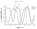
- FIG. 4 shows a time waveform when a polyethylene plate having a thickness of 500 ⁇ m and a thickness of 400 ⁇ m is used as the sample 12.
- the transmittance spectrum became an interference wave as shown in FIG. This is interference due to the above (i) and (ii).
- the transmission spectrum described in FIG. 5 was obtained as follows. First, each of the three data (ref, 400 ⁇ m, 500 ⁇ m) in the time waveform of FIG. 4 was Fourier transformed. Next, the 400 ⁇ m Fourier transform in FIG. 4 was divided by the ref Fourier transform in FIG. 4 to obtain a 400 ⁇ m transmission spectrum in FIG. 4 was divided by the Fourier transform of ref in FIG. 4 to obtain a 500 ⁇ m transmission spectrum in FIG.
- the interference was observed to be shifted depending on the optical path length propagating through the sample accompanying the thickness change.
- the transmittance was observed to change by 80% at the frequency (1.5 THz) indicated by the broken line in the figure.
- the sample is scanned in the XY direction by the XY stage 34, and the distribution of transmittance and transmission intensity can be measured by an image cut out at an arbitrary frequency.
- physical properties such as refractive index and dielectric constant can be measured.
- FIG. 6A shows the sample holder 40 of this embodiment.
- the sample holder 40 includes the reflecting member 11, the sample 12, the incident member 13, and the terahertz wave reflection suppressing layer 41.
- the same components as those in the first embodiment are denoted by the same reference numerals and description thereof is omitted.
- the feature of the sample holder 40 is that a separate layer is provided in contact with the outside (atmosphere side) of the incident member 13. This layer is a terahertz wave reflection suppressing layer 41 for suppressing the reflection of the irradiation wave I.
- the incident member 13 is made of Si material, but still reflects the irradiation wave I. If reflection occurs immediately at the time of irradiation, the efficiency of terahertz wave detection becomes low, and measurement of a very small amount of sample 12 becomes difficult. Also, the analysis of the interference waveform is complicated. Therefore, the second embodiment intends to suppress the reflection of the irradiation wave I by the configuration of the present embodiment.
- FIG. 6 (b) is an enlarged view of a portion A in FIG. 6 (a).
- the terahertz wave reflection suppressing layer 41 has a structure in which triangular protrusions 42 having a base w and a height h are periodically arranged.
- the triangular protrusion 42 may be a cone or a quadrangle.
- the material of the triangular protrusion 42 is the same Si material as the incident member 13.
- the triangular protrusions 42 are formed by etching or groove processing on the Si substrate.
- the surrounding dielectric constant including the atmosphere is gradually changed.
- the triangular protrusion 42 of the terahertz wave reflection suppressing layer 41 smoothly changes the atmospheric dielectric constant (approximately 1) to the dielectric constant of Si (approximately 3.4). As a result, the irradiation wave I is not easily reflected. Become.
- the example of the triangular protrusion 42 is shown.
- a plurality of layers having different dielectric constants may be used and a plurality of layers may be stacked so that the dielectric constant changes stepwise.
- the dielectric constant gradually changes, it functions as a terahertz wave reflection suppressing layer.
- FIG. 7 shows the sample holder 50 of this embodiment.
- the sample holder 50 includes the reflecting member 11, the sample 12, and the incident member 13.
- the same components as those in the first embodiment are denoted by the same reference numerals and description thereof is omitted.
- sample 12 is composed of a dielectric substrate 51 and a thin film 52.
- Sample 12 is obtained by sintering a dielectric ceramic material and forming a thin film 52 thereon using a thin film forming method. Naturally, the dielectric constants of the dielectric substrate 51 and the thin film 52 are different.
- the thin film 52 side may be provided in contact with the reflecting member 11.
- the dielectric substrate 51 side may be provided in contact with the reflecting member 11.
- the sample 12 when the sample 12 is formed of a plurality of layers having different dielectric constants, a more accurate measurement can be performed by analyzing the sample 12 by bringing the analysis target layer out of the plurality of layers of the sample 12 into contact with the reflecting member 11. A value can be obtained.
- Example 4 shows an example in which a polymer film called a membrane used for transfer of proteins and DNA after electrophoresis is used for detection of binding between a small molecule and a protein.
- the material of the membrane is made of polyvinylidene fluoride (PVDF).
- PVDF polyvinylidene fluoride
- the refractive index of the membrane is as low as about 1.1, and it is expected that the refractive index will increase when biopolymers adhere and permeate there. This is expected to increase the effective optical path length during reciprocation as the reflection intensity at the incident member (Si) interface decreases as the refractive index changes.
- the membrane is a porous membrane, and the binding ability to biopolymers is different due to different materials and porosity.
- examples include PDVF membrane and nitrocellulose membrane excellent in protein adsorption ability manufactured by BIO-RAD, and membrane manufactured by MILLIPORE used as a microfiltration filter.
- Membranes exhibit absorption characteristic of the terahertz wave band with various materials and can be selected according to various application methods.
- the adsorption capacity specified in the membrane specifications is not necessarily important, and a biopolymer that selectively becomes a host can be selected by chemical treatment on the membrane. It can be adsorbed.
- the low molecular weight compound itself does not interact with the membrane at all or has a very weak interaction, so that it easily flows out by washing performed after the reaction with the protein.
- a method of adding hydrophobicity to a low molecular weight compound by chemical treatment and immobilizing the membrane with a hydrophobic bond was used.
- Hydrophobic addition was performed by a known method of binding hydrophobic polyethylene glycol (PEG) to a low molecular weight compound, and the surface was bound (immobilized) to a PVDF membrane having hydrophobic characteristics.
- PEG polyethylene glycol
- a low molecular weight compound was similarly bonded to MPEG (Methyl PEG, average molecular weight 5000) having a molecular weight different from that of PEG (average molecular weight 3400), and the measurement results were compared by the difference in the immobilization method.
- MPEG Metal PEG, average molecular weight 5000
- Biotin and streptavidin which are known to form strong bonds, were used.
- Biotin was bound to PEG and MPEG, respectively, and immobilized by hydrophobic interaction with the membrane.
- concentration of biotin was changed stepwise from 1 ⁇ 10 ⁇ 3 M (M means mol / liter) to 3.2 ⁇ 10 ⁇ 6 M, and duplicates were used to confirm reproducibility.
- a dot blot was performed. The amount dropped to each was 0.2 ⁇ L, and spread on a 3 mm circle on the membrane.
- the sample thus prepared is referred to as a membrane array.
- Fig. 8 shows a schematic diagram of the membrane array prepared by the previous method, and the detection result by fluorescent labeling.
- the dark-colored portion is a portion where labeled streptavidin is detected.
- Fig. 9 shows the image results at 1.5 terahertz obtained with the THz-TDS reflection measurement system. This image is the result of unlabeled detection in which unlabeled streptavidin was reacted. The brighter the light, the greater the absorption. Similar to the fluorescence image, the presence of streptavidin could not be confirmed at the place where only the lower two rows of biotin solutions were dropped.
- linkers There are various types of substances that can be used as linkers, and there is an optimum method for small molecules and membrane types.
- Example 5 In Example 5, unlabeled detection using the present invention was performed on other biopolymers, and the presence / absence of binding between sugar and glycoprotein (lectin) was imaged. An image is shown in FIG.
- a sugar chain is a compound in which a plurality of sugars are linked.
- sugar chains present on the cell surface bind to lectins, viruses, lipids, etc., and transmit information to cells. Because it is closely related to cell growth, infection and immune function, it is said to be an important substance in life activities. However, since the binding force is not as high as the binding with antigens and antibodies, it is considered difficult to analyze the interaction.
- the reaction with a lectin exhibiting selective binding to galactose in a sugar chain was imaged by the same method as in the previous example, and an unlabeled detection was attempted.
- the sugar chain pentasaccharide, tetrasaccharide, and lactose (Lac) were immobilized on the membrane in duplicate, and lactose without immobilization treatment was used at the bottom stage.
- the unlabeled test using the membrane array of low molecular weight compounds developed from this method can be expected to be a screening technology for rapidly exploring candidate substances in the field of drug discovery.
- This method is introduced as a screening to react and image a known candidate substance array and an unknown protein group (mixture).
- the part is cut out, the molecular weight is obtained using electrophoresis, and further, the part is cut out and crystallized, and the three-dimensional structure can be examined using the X-ray structure analysis method.
- Such a utilization method is suitable for the analysis of a conventional group of difficult-to-label substances and a protein group in a mixture extracted from a living body.
- a ⁇ protein and the like are preferably used because of their high aggregation properties.
Abstract
テラヘルツ波を照射して、微小試料もしくは微量試料の組成、物性、質量、寸法を精確に測定する。 テラヘルツ波に対し透過性を有する試料12を分析するための試料分析方法である。試料12の第一の主面側に反射部材11を当接して設け、試料12の第二の主面側に入射部材13を当接して設け、入射部材13の外側から試料12に向けてテラヘルツ波を照射し、試料12の第一の主面と反射部材11との界面における第一面反射波、および、試料12の第二の主面と入射部材13との界面における第二面反射波、により生じる干渉波を利用して試料12を分析する。
Description
本発明は、テラヘルツ波を用いて試料の分析を行う技術に関する。テラヘルツ波とは、20GHzから120THzの周波数を有する電磁波をいう。分析の一例としては、試料自体の物性や寸法を測定したり、試料に付着した生体高分子の量を測定することが挙げられる。
被測定物である試料にテラヘルツ波を照射すると、その試料の物性に応じた測定結果が得られる。例えば、試料に対して波長の異なるテラヘルツ波を照射すると、試料の電磁波吸収により特定波長のテラヘルツ波が吸収されるので、テラヘルツ波の透過率の周波数特性は、試料の物性に応じた固有の波形となって現れる。
テラヘルツ波の透過率を測定する方法としては、テラヘルツ時間領域分光法(以下、THz-TDSと呼ぶ)が知られている。特許文献1の実施例2には、反射光学系によるTHz-TDSが示されている。この実施例においては、テラヘルツ波発生器から出射したテラヘルツ波が放物面鏡を経ることで試料上に集光照射され、その後、試料上を反射したテラヘルツ波を放物面鏡を用いてテラヘルツ検出器に集光している。
ここで、従来の試料保持部およびテラヘルツ波伝送経路を図11に示す。なお、図11は特許文献1の記載に基づき出願人が作成したものである。
図11のとおり、従来の試料保持部100は、被測定対象である試料102と、試料102に当接された金属膜101により構成される。金属膜101はテラヘルツ波をほぼ100%反射するミラーである。
試料102のテラヘルツ波に対する透過率を測定するため、試料102にテラヘルツ波を照射する。そのときの試料内でのテラヘルツ波伝搬経路を図11にて説明する。
まず、試料102にテラヘルツ波である照射波Iが入射される。照射波Iの一部は試料102に直接当たって反射する反射波R0となり、残りの一部は試料102内を透過する試料内伝搬波r0となる。このとき大気中と試料102との誘電率の違いにより反射波R0、試料内伝搬波r0それぞれに屈折が起きる。試料内伝搬波r0は金属膜101で反射され、試料内伝搬波r1となり、さらに試料内伝搬波r1の一部は試料102と大気の界面で反射して試料内伝搬波r2となり、残りの一部は界面を通過して出射され、出射波R1となる。
このときの反射波R0と出射波R1の振幅の大きさを時間軸で求め、フーリエ変換することにより、試料102の組成、物性、質量を求める。これが従来からあるTHz-TDSである。
しかし、この従来のTHz-TDSにおいては次のような問題があった。
1つは、試料内でのテラヘルツ波の吸収が十分に行われずに、反射波R0、出射波R1の振幅の差が試料のあるときと無いときで変わらず、十分な試料102の分析ができない問題があった。特に、試料102が微小であったり厚みが薄い場合はテラヘルツ波の伝送経路自体が短くなり、電磁波吸収が十分に行われない事態が起きる。また、試料102に含まれる測定対象物質の量が微量であったときも電磁波吸収が十分に行われず、1mg以下という微量を測定するには従来の方法では不可能であった。
さらに、試料102を面方向にスキャンして面全体の分析をする場合、試料面の凹凸が大きいと試料102からの反射波や出射波の角度が安定せず精確に測定できないという問題があった。
本発明が解決しようとする課題は、微小試料、微量試料もしくは薄層試料の組成、物性、質量、寸法を精確に測定することである。
本発明に係る試料分析方法は、テラヘルツ波に対し透過性を有する試料を分析するための試料分析方法であって、該試料の第一の主面側に反射部材を当接して設け、該試料の第二の主面側に入射部材を当接して設け、該入射部材の外側から該試料に向けてテラヘルツ波を照射し、該試料の第一の主面と該反射部材との界面における第一面反射波、および、該試料の第二の主面と該入射部材との界面における第二面反射波、により生じる干渉波を利用して該試料を分析する試料分析方法である。テラヘルツ波とは、20GHzから120THzの周波数を有する電磁波をいう。
本発明のある特定の局面では、前記試料の第一の主面と前記反射部材との界面、および、前記試料の第二の主面と前記入射部材との界面、が平行である。
本発明の他の特定の局面では、前記干渉波は、前記第一面反射波から前記試料および前記入射部材を通過して出射された出射波と、前記第二面反射波から前記入射部材を通過して出射された出射波と、により生じるものである。
本発明の別の特定の局面では、前記干渉波は、前記試料の第一の主面と前記反射部材との界面、および、前記試料の第二の主面と前記入射部材との界面、におけるテラヘルツ波の反射が複数回行われた多重反射波から形成される。多重反射波とは、試料に向けてテラヘルツ波を照射してから出射されるまでの過程において、試料と反射部材との界面、および試料と入射部材との界面において複数回反射した反射波をいう。
本発明のさらに他の局面では、前記反射部材の屈折率は前記試料の屈折率より大きく、前記入射部材の屈折率は前記試料の屈折率より大きく、かつ、前記入射部材の屈折率は前記入射部材の外側に存在する大気の屈折率より大きい。
本発明のさらに別の局面では、前記入射部材の外側に当接してテラヘルツ波反射抑制層を設ける。
本発明のまたさらに他の局面では、試料分析方法は、前記試料が誘電率の異なる複数層で形成されているときの試料分析方法であって、前記試料の複数層のうちの分析対象となる層を前記反射部材に当接して該試料を分析する。
本発明のまたさらに別の局面では、試料分析方法は、テラヘルツ波に対し透過性を有する試料を分析するための試料分析方法であって、該試料の第一の主面側に反射部材を当接して設け、該試料の第二の主面側に入射部材を当接して設け、該入射部材の外側から該試料に向けてテラヘルツ波を照射し、該試料の第一の主面と該反射部材との界面における反射波と、該試料の第二の主面と該入射部材との界面における反射波と、該入射部材と該入射部材の外側の界面における反射波と、を生じさせた後、最終的に該入射部材を透過して外側へ出射された複数の出射波により生じる干渉波を利用して該試料を分析する試料分析方法である。最終的に外側へ出射された出射波とは、試料や入射部材内を1回であろうが複数回であろうが伝搬した後に、結局、外側へ出射されることになったテラヘルツ波をいう。
本発明による試料分析方法によれば、微小試料、微量試料もしくは薄層試料の組成、物性、質量、寸法を精確に測定することができる。
本発明の実施形態として、本発明が従来技術と大きく異なる点を中心に説明する。従来技術と異なる点は、試料保持部10および試料保持部内でのテラヘルツ波の伝送経路にある。なお、テラヘルツ波の光源、光学系、データ処理方法等については実施例にて具体的に説明する。
図1を用いて本実施形態の試料保持部10および試料保持部内でのテラヘルツ波伝搬経路の説明をする。本実施形態の試料保持部10は、被測定対象である試料12と、試料12の一方の主面に当接された反射部材11と、試料12のもう一方の主面に当接された入射部材13により構成される。
反射部材11は試料12より屈折率が大きくテラヘルツ波をほぼ100%反射するミラーである。その他に、メタマテリアルのように負の屈折率を有する部材を用いることもできる。
入射部材13は試料12と屈折率が異なり、かつ、大気よりも屈折率が大きい材料からなる。より好ましくは、入射部材13の屈折率は試料12の屈折率より大きいほうがよく、例えば入射部材13の材料としては高抵抗シリコン(Si)や透光性セラミックが用いられる。後に説明する多重反射を有効に使えるからである。
試料12はテラヘルツ波に対し、透過性、吸収性を有する素材である。
ここで、反射部材11と試料12の間の境界を第一界面21と呼び、試料12と入射部材13の間の境界を第二界面22と呼び、入射部材13と大気との間の境界を第三界面23と呼ぶ。さらに第一界面21にて生じる反射波を第一面反射波と呼び、第二界面22にて生じる反射波を第二面反射波と呼び、第三界面23にて生じる反射波を第三面反射波と呼ぶ。
本発明は、第一界面21にて生じる第一面反射波、および、第二界面22にて生じる第二面反射波、により生じる干渉波を利用して試料12を分析することに特徴がある。以下、その説明を行う。
まず、入射部材13の外側(大気側)から試料保持部10に向けてテラヘルツ波が照射される。この照射波Iは第三界面23を通過し入射部材内伝搬波t0となる。このとき大気と入射部材13との誘電率の違いによりテラヘルツ波に屈折が起きる。入射部材内伝搬波t0の一部は試料12に入射し、残りの一部は第二界面22にて反射して入射部材内伝搬波t1(反射波)となる。入射部材内伝搬波t1の一部は第三界面23で反射して入射部材内伝搬波t2(反射波)となり、残りの一部は第三界面を通過して出射波R1として出射される。
一方、試料12に入射された伝搬波は試料内伝搬波r0となって所定の角度をもって試料内を伝搬する。所定の角度は、入射部材13と試料12の誘電率の違いにより決まる。試料内伝搬波r0は第一界面21で反射され、試料内伝搬波r1(反射波)となる。さらに試料内伝搬波r1の一部は第二界面22を反射するが、残りの一部は第二界面22を通過して更に第三界面23を通過して出射波R2となって出射される。第三界面23を通過せずに反射した波は入射部材内伝搬波r1t2(反射波)となる。
試料内伝搬波r1から第二界面22で反射した伝搬波は試料内伝搬波r2となる。試料内伝搬波r2は第一界面21で反射したのち、一部が第二界面22を通過して更に一部が第三界面23を通過して出射され、もうひとつの出射波R3となる。
このときの出射波R1と出射波R2により形成される干渉波の振幅の大きさを時間軸で求め、フーリエ変換することにより、試料12の組成、物性、質量、寸法を求めることができる。また、出射波R1と出射波R2および出射波R3より形成される干渉波の振幅の大きさを時間軸で求め、フーリエ変換することもできる。さらに、第一界面21、第二界面22、第三界面23での多重反射により形成される干渉波の振幅の大きさを時間軸で求め、フーリエ変換することにより、より精確に試料12の組成、物性、質量、寸法を求めることができる。
従来技術のTHz-TDSでは試料を面内方向に走査して多点測定を行う際、試料面の凹凸が大きいと試料102からの反射波R0や出射波R1(図11のR0、R1)の角度が安定せず精確に測定できない問題があった。
それに対し本発明は図1のように、試料保持部10に表面平滑な入射部材13を設けたので、第二界面22からの反射波の角度を安定して計測できる利点がある。さらに、本発明は試料保持部10に表面平滑な入射部材13を設け、第二界面22と検出素子36の距離を一定にしたので、試料を面内方向に走査して多点測定を行う際、第二界面22からの反射波を同じ時間基準で計測できる利点がある。そのため試料12の物性等を精確に測定できるようになった。
従来技術のTHz-TDSでは、試料102が微小であったり厚みが薄い場合は試料内のテラヘルツ波の伝送経路自体が短くなり電磁波吸収が十分に行われず精確に測定できないという問題があった。また、試料102に含まれる測定対象物質の量が微量であった場合も電磁波吸収が十分に行われず精確に測定できないという問題が起きた。
それに対し本発明は、試料保持部10に表面平滑な入射部材13を設け、第二界面および第一界面でのテラヘルツ波の多重反射を積極的に用いることにより、テラヘルツ波の伝送経路を実質的に長くして、微小微量な試料でも測定可能にしている。
従来技術のTHz-TDSでは、試料102を測定装置に配置するまでに、試料表面が大気中に触れるのでその間に大気中の不純物が付着し精確な測定の妨げとなっていた。それに対し本発明は、試料12を反射部材11と入射部材13で挟み込むので、試料12が大気中に直接触れることはなくなり、不純物が後に付着するという問題も解決できる。
さらにここで、比較例としてATR(attenuated total reflection)法を挙げ、比較例と本発明の対比を行う。
ATR法は赤外光を用いた赤外分光分析法である。図12に示したとおり、試料202と、それより屈折率の大きいSi(シリコン)プリズム203を接触させ、赤外光である照射波Iの入射角を調整し、プリズム内部で全反射が起こるようにして出射波R1を測定する方法である。
このとき赤外光は試料202にわずかに、所定の深さだけ入り込んでから反射するので、試料202表面の赤外吸収スペクトルが得られる。このスペクトルを解析することにより試料202の構造解析や定性定量分析を行うことができる。このように試料202に所定の深さだけ入り込むエバネッセント波Eを用いるのがATR法の特徴である。
また、図12のようにプリズム内での多重反射を用いたATR法では、プリズム203の長さと厚さと光源から出た照射波Iの入射角度で決まる多重反射回数が試料202のサンプリング回数となる。
本発明は次に示す点でATR法と異なる。本発明とATR法ではテラヘルツ波の多重反射を用いる点で同じであるが、ATR法は試料202の外表面で全反射を起こさせプリズム203内で起きた多重反射を利用しているのに対し、本発明は試料12内で起きた多重反射も利用している点で原理が異なる。
試料表面による電磁波の吸収を利用するATR法より、試料内における電磁波吸収を利用する本発明は、電磁波の吸収が起き易く、試料12の微小微量検出に適している。
また、ATR法は入射部材内(プリズム内)での多重反射であり、試料内での多重反射を利用しないので、テラヘルツ波を透過してしまう試料の測定には適していない。本発明はテラヘルツ波を透過する試料12に適した測定方法であり、かつ、試料内の多重反射を利用しているという点でATR法とは全く異なる方法である。
以上が、本発明が従来技術と大きく異なる点である。以下、図面を参照しつつ本発明の実施例を具体的に説明する。
(実施例1)
図2は、テラヘルツ時間領域分光法(THz-TDS)を用いたイメージングシステム30である。イメージングシステム30は、THz-TDSの光路中に試料駆動用のXYステージ34を配置し、試料12のラスタスキャンにより画像を取得できるように構成されており、各周波数での透過率画像や、吸光度画像を得ることができる。
図2は、テラヘルツ時間領域分光法(THz-TDS)を用いたイメージングシステム30である。イメージングシステム30は、THz-TDSの光路中に試料駆動用のXYステージ34を配置し、試料12のラスタスキャンにより画像を取得できるように構成されており、各周波数での透過率画像や、吸光度画像を得ることができる。
テラヘルツ波は、バイアス電圧を印加した光スイッチ(発生素子32)にフェムト秒パルスレーザーを当てた際に生じるキャリアによって瞬時電流を生じさせ、この時間微分に比例したテラヘルツパルス波を発生させることにより出力される。一方、テラヘルツ波の光スイッチ(検出素子36)はこの反対の構成をとっており、電圧を印加する代わりに電流計を取り付けている。
テラヘルツ波発生時と同様にフェムト秒レーザーをアンテナのギャップに照射して光キャリアを生成させると、ギャップ領域の電気伝導度が増加して一時的にアンテナ回路が閉じた状態になる。この時、テラヘルツ波が検出素子36に到着していると、検出素子36にテラヘルツ波の電場による電界が加わることによってアンテナ回路にテラヘルツ波の振幅に比例した電流が流れ、その電流値が検出される。
また、プローブ光とテラヘルツ波の間に光学遅延を与えることにより、その光学遅延に応じた時刻のテラヘルツ波の電場強度を検出することができる。THz-TDSではこの光学遅延により生じた僅かに異なる時間の電場強度を測定し、ひとつの時間波形とするサンプリング法を用いる。このようにして得られた時間波形をフーリエ変換し、位相と強度両方の周波数スペクトルに変換することがTHz-TDSの大きな特長である。
イメージングシステム30では、波長840nm、出力650mW、パルス幅100fs以下、繰り返し周波数80MHzのフェムト秒レーザーを使用し、光スイッチ32、36には低温成長型GaAs膜(Low-temperature grown GaAs、LT-GaAs)を用いた。
図3は試料12の具体的な固定方法を示したものである。試料12の第一の主面(図3において上側)および第二の主面(図3において下側)にそれぞれ反射部材11、入射部材13を配置した状態で固定する。次に、穴の開いた下側保持プレート15に下側凸形状の入射部材13をはめ込み、入射部材13の上から上側保持プレート14を重ね、その後、取り付けネジ16でこれらを固定する。このとき、試料12の第一の主面と第二の主面は平行となり、厚みのばらつきは1%以内であった。
試料12の第一の主面と第二の主面を平行にすることにより、第一界面21と検出素子36との距離、および第二界面22と検出素子36との距離をそれぞれ一定にでき、試料を面内方向に走査して多点測定を行う際、界面からの反射波を同じ時間基準で計測できる利点がある。
試料12を入れる試料室(図示せず)およびレーザー光路は、水蒸気の影響を取り除くために、窒素パージを行ってから測定を行う。
図2にイメージングシステム30の光学系概略図を示す。光スイッチ32から放射されたテラヘルツ波は放物面鏡33で反射され、試料12の置かれた集光位置に入射される。被測定対象となる試料12はXYステージ34に載置され、二次元的に移動してポイント毎に分光測定を行いながら、順次XYステージ34を動かしてイメージングを行う。
本実施例における反射測定系では、光スイッチ32から放射されたテラヘルツ波は放物面鏡33(f=237.1mm、NA=0.26)により集光され、試料12に対して下から20°の角度で斜め入射する。
試料保持部10からの反射波を測定して面方向にスキャンする際、試料面は平滑で傾きを持たないことが望ましい。
また、本実施例では、高抵抗シリコン(Si)単結晶(抵抗率10kΩ・cm以上)による入射部材13を試料面に当接して設置した。高抵抗シリコン(Si)はテラヘルツ波の吸収ロスが小さく入射部材に適している。
Siはテラヘルツ波帯における屈折率が3.415と一定であり、ポリエチレンなどのプラスチック素材より屈折率が大きいため空気からSiにテラヘルツ波が入射する際の損失は大きいが、テラヘルツ波帯におけるSiの吸収係数は小さく、Si内部でのテラヘルツ波の損失がほぼ0と見なすことができる。このSi材の入射部材13を設けたことにより、テラヘルツ波は集光しながら5.8度の入射角で試料12に入射することとなる。
本実施例の反射測定系ではSi表面と試料12との界面からの反射波が検出されるが、検出する試料が微小微量であることから、図3に示すように試料12のもう一方の面に反射部材11となるミラーを配置し、往復分の光路長による吸収を期待した光学系とした。
これらの影響を確認するために厚みの異なるポリエチレン板を試料12とし、反射測定系(試料12の上面にミラーを配置した系)による時間波形ならびに周波数スペクトルを比較した。
図4に板厚500μmと板厚400μmのポリエチレン板を試料12としたときの時間波形を示す。図4右下に示すように、(i)シリコンと試料(サンプル)界面での反射、(ii)試料上面のミラーからの反射、(iii)2往復目のミラーからの反射信号が時間波形に観測された。この結果をフーリエ変換し周波数軸のグラフで表すと、図5に示すように、透過率スペクトルが干渉波となった。これは、先述の(i)や(ii)による干渉である。
図5に記載されている透過スペクトルは以下のようにして求めた。まず、図4の時間波形における3つのデータ(ref、400μm、500μm)それぞれをフーリエ変換した。次に、図4の400μmのフーリエ変換を図4のrefのフーリエ変換で割って求め、図5の400μmの透過スペクトルとした。また、図4の500μmのフーリエ変換を図4のrefのフーリエ変換で割って求め、図5の500μmの透過スペクトルとした。
図5からわかるとおり、厚み変化に伴う試料内を伝搬する光路長に応じて干渉がずれて観測された。この結果、厚みが100μmしか変わらないポリエチレンの板でも、図中破線で示す周波数(1.5THz)において、透過率が80%も変化して観測された。
このような測定系においては、試料をXYステージ34でXY方向にスキャンし、任意の周波数で切り出した画像により、透過率や透過強度の分布を測定することができる。その他にも、屈折率や誘電率などの物性値も測定可能となる。
(実施例2)
図6(a)に本実施例の試料保持部40を示す。試料保持部40は、反射部材11、試料12、入射部材13およびテラヘルツ波反射抑制層41からなる。実施例1と同じ構成には同じ符号を付し説明を省略する。
図6(a)に本実施例の試料保持部40を示す。試料保持部40は、反射部材11、試料12、入射部材13およびテラヘルツ波反射抑制層41からなる。実施例1と同じ構成には同じ符号を付し説明を省略する。
試料保持部40の特徴は、入射部材13の外側(大気側)に当接して別層を設けたことにある。この層は、照射波Iの反射を抑制するためのテラヘルツ波反射抑制層41である。
実施例1で説明したとおり、入射部材13はSi材であるが、それでも少なからず照射波Iを反射する。照射の時点ですぐに反射が起きるとテラヘルツ波検出の効率が低くなってしまい、微小微量な試料12の測定が難しくなる。また、干渉波形の解析も複雑になる。そこで、本実施例の構成により照射波Iの反射を抑えようというのが実施例2の意図するところである。
図6(b)は、図6(a)のA部の拡大図である。図6(b)に示したとおり、テラヘルツ波反射抑制層41は、底辺w、高さhの三角突起42を周期的に配列した構造からなる。三角突起42は円錐でも四角推でもよい。
三角突起42の材質は入射部材13と同じSi材である。三角突起42はSi基板に対するエッチング、もしくは溝加工により形成される。
このような三角突起42を有することにより、大気を含めた周囲の誘電率が徐々に変化する状態を作り出している。テラヘルツ波反射抑制層41の三角突起42により、大気の誘電率(およそ1)からSiの誘電率(およそ3.4)への変化が滑らかに行われ、その結果、照射波Iが反射しにくくなる。
なお、実施例2では三角突起42の例を示したが、他の例として、誘電率の異なる層を複数用いて、誘電率が段階的に変化するように複数重ねた構造としてもよい。要するに誘電率が徐々に変化する状態となっていればテラヘルツ波反射抑制層として機能する。
(実施例3)
図7に本実施例の試料保持部50を示す。試料保持部50は、反射部材11、試料12、入射部材13からなる。実施例1と同じ構成には同じ符号を付し説明を省略する。
図7に本実施例の試料保持部50を示す。試料保持部50は、反射部材11、試料12、入射部材13からなる。実施例1と同じ構成には同じ符号を付し説明を省略する。
試料保持部50の特徴は、試料12が誘電体基板51と薄膜52で構成される点である。試料12は誘電体セラミック材を焼結し、その上に薄膜形成法を用いて薄膜52を形成したものである。誘電体基板51と薄膜52の誘電率は当然異なる。
このような試料12の場合、どちらを主に測定したいかで試料12の上下の向きを変え、より精確な測定結果を得ることができる。例えば薄膜52についての物性を主に測定したい場合は、薄膜52側を反射部材11に当接して設ければよい。誘電体基板51についての物性を主に測定したい場合は、誘電体基板51側を反射部材11に当接して設ければよい。
すなわち、試料12が誘電率の異なる複数層で形成されているときは、試料12の複数層のうちの分析対象となる層を反射部材11に当接して、試料12を分析するとより精確な測定値を得ることができる。
(実施例4)
実施例4では、電気泳動後のタンパク質やDNAの転写に用いられるメンブレンと呼ばれる高分子膜を、小分子とタンパク質の結合検出のために用いた例を示す。メンブレンの材質はポリフッ化ビニリデン(PVDF)からなる。このメンブレンに生体高分子を付着させた試料の分析例を以下に示す。
実施例4では、電気泳動後のタンパク質やDNAの転写に用いられるメンブレンと呼ばれる高分子膜を、小分子とタンパク質の結合検出のために用いた例を示す。メンブレンの材質はポリフッ化ビニリデン(PVDF)からなる。このメンブレンに生体高分子を付着させた試料の分析例を以下に示す。
メンブレンの屈折率は約1.1と低く、そこに生体高分子が付着、浸透することで屈折率が大きくなる事が期待される。このことは屈折率変化に伴う入射部材(Si)界面での反射強度の減少とともに、往復時の実効的な光路長が長くなる事が予想される。
メンブレンは多孔質の膜であり、材質や空隙率が異なることで、生体高分子に対する結合能が異なる。例として、BIO-RAD社製のタンパク質吸着能に優れたPDVFメンブレンとニトロセルロースメンブレンおよび、精密ろ過フィルターとして使用されるMILLIPORE社製のメンブレンなどが挙げられる。
メンブレンは、さまざまな材質でテラヘルツ波帯に特徴的な吸収を示すことから、各種応用法に合わせて選択することが可能である。また、タンパク質やDNAなどの分析を行う際に、メンブレンの仕様として明記されている吸着能が必ずしも重要ではなく、メンブレン上に化学的な処理を行うことで選択的にホストとなる生体高分子を吸着できるようになる。
DNAのような液体サンプルを基板上に滴下し、乾燥させてTHz-TDSなどで分光測定を行う際、乾燥ムラにより試料の状態が不均一になり測定結果に影響を与えることがある。しかし、メンブレンのように浸透性のある基板を採用することにより、その問題を解決できることも知られている。
低分子化合物そのものは、メンブレンとまったく相互作用しないか、極めて弱い相互作用しかしないため、タンパク質との反応後に行う洗浄によって容易に流れ出してしまう。
そこで本実施例では、低分子化合物に化学処理によって疎水性を付加し、メンブレンと疎水結合によって固定化する方法を用いた。疎水性の付加には、低分子化合物に疎水性ポリエチレングリコール(PEG)を結合する公知の手法で疎水性を与え、表面が疎水性の特性を持つPVDFメンブレンに結合(固定化)させた。
なお、本実施例ではPEG(平均分子量3400)と分子量の異なるMPEG(Methyl PEG、平均分子量5000)においても同様に低分子化合物を結合させ、固定化法の違いによる測定結果の比較を行った。
低分子化合物とタンパク質は、強固な結合をすることで知られているビオチンとストレプトアビジンを用いた。ビオチンをPEGとMPEGにそれぞれ結合させ、メンブレンとの疎水性相互作用により固定化した。固定化の際、ビオチンは1×10⁻³M(Mはモル/リットルの意味)から3.2×10-6Mまで濃度を段階的に変化させ、再現性を確認するために各2連でドットブロットを行った。それぞれに滴下した量は0.2μリットルずつで、メンブレン上では約3mmの円状に広がった。
その後、未処理のメンブレン上にストレプトアビジンが結合することを防ぐために、スキムミルクでブロッキング処理を施した。以後、このように作成された試料をメンブレンアレイと記す。
一方、ストレプトアビジンの結合を確認するために、同様の処理を行って作成したメンブレンアレイに対し、蛍光標識(Alexa633:Alexa Fluorは登録商標)付のストレプトアビジンを反応させて、別途蛍光検出にて結合の確認を行った。
図8に先の方法で作成したメンブレンアレイの模式図と、蛍光標識による検出結果を示す。図8右図の蛍光画像において濃い色に見える部分が標識されたストレプトアビジンが検出されている箇所である。
メンブレンに固定化せず、ビオチン溶液を滴下しただけの下段2列は、洗浄過程でメンブレンからビオチンが洗い流されたため、ストレプトアビジンと結合できなかった。このことから、PEGによるビオチンの固定化が正しく出来ており、そのビオチンがストレプトアビジンとの結合能を有していることが確認できた。
THz-TDSの反射測定系で得た1.5テラヘルツでの画像結果を図9に示す。こちらの画像は標識無しのストレプトアビジンを反応させた非標識検出の結果で、明るいほど吸収が大きいことを示す。蛍光画像と同様に、下段2列のビオチン溶液のみを滴下した場所ではストレプトアビジンの存在が確認できなかった。
さらにMPEGを使ってメンブレン上にビオチンを固定化した方の反応性が高く、この結果は蛍光法による傾向と同じであった。
このようなリンカーとなる物質はさまざまなものが報告されており、小分子やメンブレンの種類に合わせた最適な手法がある。
またわずかではあるが、蛍光画像では確認できていない低濃度(1.6×10⁻⁵M)でも吸収が見られ、Alexa633を用いた蛍光検出よりも少ない量まで検出できている。
(実施例5)
実施例5では、他の生体高分子に対して本発明を用いた非標識検出を行っており、糖と糖蛋白(レクチン)の結合についての結合の有無を画像化した。画像化したものを図10に示す。
実施例5では、他の生体高分子に対して本発明を用いた非標識検出を行っており、糖と糖蛋白(レクチン)の結合についての結合の有無を画像化した。画像化したものを図10に示す。
糖鎖は複数の糖が連なった化合物で、特に細胞表面上に存在する糖鎖はレクチンやウイルス、脂質などと結合し、細胞に情報を伝達する。細胞の成長や感染、免疫機能などと密接に関連することから、生命活動においても重要な物質と言われている。しかし、結合力が抗原や抗体との結合のように高くないことから、相互作用の分析が難しいとされている。
本実施例では、糖鎖中のガラクトースに選択的な結合性を示すレクチンとの反応を先の実施例と同じ方法でイメージングし、非標識検出を試みた。糖鎖は、5糖、4糖、ラクトース(Lac)をそれぞれ上下2連ずつメンブレンに固定化し、一番下の段には固定化処理を行わないラクトースを用いた。
その結果、先のビオチンのメンブレンアレイと同様に、固定化していない場合は洗浄などの処理によりメンブレンからはがれ落ち、レクチンと反応できていない様子が確認できた。
また、5糖や4糖の方がラクトースよりもレクチンと反応性が高い結果が得られたことは、各分子あたり5糖、4糖にはガラクトースが2個、ラクトースにはガラクトースが1個含まれることから妥当な結果と考えられる。
本手法を発展させた低分子化合物のメンブレンアレイによる非標識検査は、創薬分野において候補物質を迅速に探査するスクリーニング技術になりうると期待できる。
スクリーニングとして本手法を導入し、既知の候補物質アレイと未知のタンパク質群(混合物)とを反応、画像化する。その結果、結合が見つかるとその部分を切り出し、電気泳動法を利用して分子量を求め、さらにその部分を切り出して結晶化し、X線構造解析法を利用して立体構造を調べることが可能となる。こういった利用法は、従来の標識化が困難な物質や、生体から抽出した混合物の状態のタンパク質群の分析に適している。例えば、Aβタンパク質などは、凝集性が高いので、好適に用いられる。
10 試料保持部
11 反射部材
12 試料
13 入射部材
21 第一界面
22 第二界面
23 第三界面
31 レーザ光源部
32 光スイッチ(発生素子)
33、35 放物面鏡
34 XYステージ
36 光スイッチ(検出素子)
37 データ処理部
I 照射波
t0、t1、t2、t3、r1t1、r2t1 入射部材内伝搬波
r0、r1、r2、r3、t2r0 試料内伝搬波
R1、R2、R3 出射波
R0 反射波
11 反射部材
12 試料
13 入射部材
21 第一界面
22 第二界面
23 第三界面
31 レーザ光源部
32 光スイッチ(発生素子)
33、35 放物面鏡
34 XYステージ
36 光スイッチ(検出素子)
37 データ処理部
I 照射波
t0、t1、t2、t3、r1t1、r2t1 入射部材内伝搬波
r0、r1、r2、r3、t2r0 試料内伝搬波
R1、R2、R3 出射波
R0 反射波
Claims (8)
- テラヘルツ波に対し透過性を有する試料を分析するための試料分析方法であって、
該試料の第一の主面側に反射部材を当接して設け、
該試料の第二の主面側に入射部材を当接して設け、
該入射部材の外側から該試料に向けてテラヘルツ波を照射し、
該試料の第一の主面と該反射部材との界面における第一面反射波、および、該試料の第二の主面と該入射部材との界面における第二面反射波、により生じる干渉波を利用して該試料を分析する試料分析方法。 - 前記試料の第一の主面と前記反射部材との界面、および、前記試料の第二の主面と前記入射部材との界面、が平行であることを特徴とする請求項1に記載の試料分析方法。
- 前記干渉波は、前記第一面反射波から前記試料および前記入射部材を通過して出射された出射波と、前記第二面反射波から前記入射部材を通過して出射された出射波と、により生じるものであることを特徴とする請求項1または2に記載の試料分析方法。
- 前記干渉波は、前記試料の第一の主面と前記反射部材との界面、および、前記試料の第二の主面と前記入射部材との界面、におけるテラヘルツ波の反射が複数回行われた多重反射波から形成されることを特徴とする請求項1~3のいずれかに記載の試料分析方法。
- 前記反射部材の屈折率は前記試料の屈折率より大きく、前記入射部材の屈折率は前記試料の屈折率より大きく、かつ、前記入射部材の屈折率は前記入射部材の外側に存在する大気の屈折率より大きいことを特徴とする請求項1~4のいずれかに記載の試料分析方法。
- 前記入射部材の外側に当接してテラヘルツ波反射抑制層を設けたことを特徴とする請求項1~5のいずれかに記載の試料分析方法。
- 前記試料が誘電率の異なる複数層で形成されているときの試料分析方法であって、前記試料の複数層のうちの分析対象となる層を前記反射部材に当接して該試料を分析することを特徴とする請求項1~5のいずれかに記載の試料分析方法。
- テラヘルツ波に対し透過性を有する試料を分析するための試料分析方法であって、
該試料の第一の主面側に反射部材を当接して設け、
該試料の第二の主面側に入射部材を当接して設け、
該入射部材の外側から該試料に向けてテラヘルツ波を照射し、
該試料の第一の主面と該反射部材との界面における反射波と、
該試料の第二の主面と該入射部材との界面における反射波と、
該入射部材と該入射部材の外側の界面における反射波と、を生じさせた後、
最終的に該入射部材を透過して外側へ出射された複数の出射波により生じる干渉波を利用して該試料を分析する試料分析方法。
Priority Applications (2)
| Application Number | Priority Date | Filing Date | Title |
|---|---|---|---|
| JP2010533790A JP5028529B2 (ja) | 2008-10-14 | 2009-09-18 | 試料分析方法 |
| US13/086,759 US8514403B2 (en) | 2008-10-14 | 2011-04-14 | Sample analysis method |
Applications Claiming Priority (2)
| Application Number | Priority Date | Filing Date | Title |
|---|---|---|---|
| JP2008265415 | 2008-10-14 | ||
| JP2008-265415 | 2008-10-24 |
Related Child Applications (1)
| Application Number | Title | Priority Date | Filing Date |
|---|---|---|---|
| US13/086,759 Continuation US8514403B2 (en) | 2008-10-14 | 2011-04-14 | Sample analysis method |
Publications (1)
| Publication Number | Publication Date |
|---|---|
| WO2010044193A1 true WO2010044193A1 (ja) | 2010-04-22 |
Family
ID=42106370
Family Applications (1)
| Application Number | Title | Priority Date | Filing Date |
|---|---|---|---|
| PCT/JP2009/004735 WO2010044193A1 (ja) | 2008-10-14 | 2009-09-18 | 試料分析方法 |
Country Status (3)
| Country | Link |
|---|---|
| US (1) | US8514403B2 (ja) |
| JP (1) | JP5028529B2 (ja) |
| WO (1) | WO2010044193A1 (ja) |
Cited By (17)
| Publication number | Priority date | Publication date | Assignee | Title |
|---|---|---|---|---|
| EP2167914A1 (en) * | 2007-07-12 | 2010-03-31 | Picometrix, LLC | System and method to measure the transit time position(s) of pulses in a time domain data |
| JP2011232289A (ja) * | 2010-04-30 | 2011-11-17 | Pola Chem Ind Inc | テラヘルツ波を用いた皮膚角層の計測方法 |
| WO2011152285A1 (ja) * | 2010-06-04 | 2011-12-08 | 日本電気株式会社 | 反射型イメージング装置およびイメージ取得方法 |
| GB2482378A (en) * | 2010-07-07 | 2012-02-01 | Melys Diagnostics Ltd | Determining analyte concentration using optical assembly interference pattern |
| JP2013004578A (ja) * | 2011-06-13 | 2013-01-07 | Hitachi High-Tech Control Systems Corp | ウェーハ接合強度検査装置及び方法 |
| JP2013024639A (ja) * | 2011-07-19 | 2013-02-04 | Murata Mfg Co Ltd | 被測定物の測定方法 |
| JP2013053916A (ja) * | 2011-09-02 | 2013-03-21 | Central Research Institute Of Electric Power Industry | 塗膜下鋼材腐食の検出方法、検出装置及び検出プログラム |
| US8969805B2 (en) | 2012-10-09 | 2015-03-03 | The University Of Tokyo | Terahertz wave measurement device and method |
| JP2015513067A (ja) * | 2012-01-23 | 2015-04-30 | ザ・リージェンツ・オブ・ザ・ユニバーシティ・オブ・ミシガンThe Regents Of The University Of Michigan | プラズモン電極を有する光伝導装置 |
| JP2016053527A (ja) * | 2014-09-03 | 2016-04-14 | 国立大学法人京都大学 | 水分量測定方法 |
| JP2016053528A (ja) * | 2014-09-03 | 2016-04-14 | 国立大学法人京都大学 | テラヘルツ波を用いた皮膚角層水分量の計測方法 |
| JP2017168595A (ja) * | 2016-03-15 | 2017-09-21 | 株式会社東芝 | 半導体レーザ装置 |
| JP2019020293A (ja) * | 2017-07-19 | 2019-02-07 | 浜松ホトニクス株式会社 | テラヘルツ波分光計測装置およびテラヘルツ波分光計測方法 |
| US10863895B2 (en) | 2015-05-27 | 2020-12-15 | The Regents Of The University Of California | Terahertz endoscopy through laser-driven terahertz sources and detectors |
| JP2021135188A (ja) * | 2020-02-27 | 2021-09-13 | アイレック技建株式会社 | 収納物検査装置 |
| US11249017B2 (en) | 2017-04-20 | 2022-02-15 | The Regents Of The University Of California | Systems and methods for high frequency nanoscopy |
| US11906424B2 (en) | 2019-10-01 | 2024-02-20 | The Regents Of The University Of California | Method for identifying chemical and structural variations through terahertz time-domain spectroscopy |
Families Citing this family (12)
| Publication number | Priority date | Publication date | Assignee | Title |
|---|---|---|---|---|
| JP2013238401A (ja) * | 2012-05-11 | 2013-11-28 | Canon Inc | 電磁波を用いる測定装置及び測定方法 |
| US9370465B2 (en) * | 2012-10-09 | 2016-06-21 | Bwt Property, Inc. | Smart IV bag with optical IV drug identification tag |
| JP2014122875A (ja) * | 2012-11-26 | 2014-07-03 | Canon Inc | 層状物体の測定装置および方法 |
| JP2014209094A (ja) * | 2013-03-29 | 2014-11-06 | キヤノン株式会社 | テラヘルツ波を用いて試料の情報を取得する情報取得装置および情報取得方法 |
| JP2015083964A (ja) * | 2013-09-17 | 2015-04-30 | キヤノン株式会社 | テラヘルツ波を用いて検体の情報を取得する情報取得装置および情報取得方法 |
| JP2016090550A (ja) * | 2014-11-11 | 2016-05-23 | パイオニア株式会社 | 情報取得装置及び固定具 |
| CN105811118B (zh) * | 2016-03-16 | 2019-08-20 | 深圳光启高等理工研究院 | 一种天线 |
| US11099001B2 (en) * | 2016-12-06 | 2021-08-24 | Pioneer Corporation | Inspection apparatus, inspection method, computer program and recording medium |
| CN111886473B (zh) | 2018-03-22 | 2022-04-12 | 3M创新有限公司 | 具有单个基准表面的时域太赫兹测量系统 |
| US10539504B1 (en) * | 2018-09-30 | 2020-01-21 | Agilent Technologies, Inc. | Method and apparatus for automating contact between an ATR crystal and a specimen |
| US20230003642A1 (en) * | 2019-10-31 | 2023-01-05 | The Regents Of The University Of California | Methods and Systems for Detecting Water Status in Plants Using Terahertz Radiation |
| JP2022154998A (ja) * | 2021-03-30 | 2022-10-13 | 横河電機株式会社 | 測定装置及び測定方法 |
Citations (6)
| Publication number | Priority date | Publication date | Assignee | Title |
|---|---|---|---|---|
| WO2003058212A1 (en) * | 2001-12-28 | 2003-07-17 | Nikon Corporation | Spectral measuring device |
| JP2004101510A (ja) * | 2002-07-15 | 2004-04-02 | Tochigi Nikon Corp | パルス光を用いた分光計測方法および装置 |
| JP2004198250A (ja) * | 2002-12-18 | 2004-07-15 | Tochigi Nikon Corp | 時間分解反射測定方法およびテラヘルツ時間分解反射測定装置 |
| WO2006030756A1 (ja) * | 2004-09-13 | 2006-03-23 | The University Of Tokyo | 高周波電磁波を用いた計測方法及び計測装置 |
| JP2007192607A (ja) * | 2006-01-18 | 2007-08-02 | Canon Inc | 積層体の情報を検出する検出装置 |
| JP2008175794A (ja) * | 2007-01-17 | 2008-07-31 | Tohoku Univ | 反射測定装置および方法 |
Family Cites Families (4)
| Publication number | Priority date | Publication date | Assignee | Title |
|---|---|---|---|---|
| DE10033259C2 (de) * | 2000-07-10 | 2003-06-26 | Univ Braunschweig Tech | Optisches Bauelement |
| GB2425833B (en) * | 2004-01-19 | 2007-02-21 | David Alexander Crawley | Terahertz Radiation Sensor and Imaging System |
| JP2006275910A (ja) * | 2005-03-30 | 2006-10-12 | Canon Inc | 位置センシング装置及び位置センシング方法 |
| JP5132146B2 (ja) | 2006-03-17 | 2013-01-30 | キヤノン株式会社 | 分析方法、分析装置、及び検体保持部材 |
-
2009
- 2009-09-18 JP JP2010533790A patent/JP5028529B2/ja active Active
- 2009-09-18 WO PCT/JP2009/004735 patent/WO2010044193A1/ja active Application Filing
-
2011
- 2011-04-14 US US13/086,759 patent/US8514403B2/en active Active
Patent Citations (6)
| Publication number | Priority date | Publication date | Assignee | Title |
|---|---|---|---|---|
| WO2003058212A1 (en) * | 2001-12-28 | 2003-07-17 | Nikon Corporation | Spectral measuring device |
| JP2004101510A (ja) * | 2002-07-15 | 2004-04-02 | Tochigi Nikon Corp | パルス光を用いた分光計測方法および装置 |
| JP2004198250A (ja) * | 2002-12-18 | 2004-07-15 | Tochigi Nikon Corp | 時間分解反射測定方法およびテラヘルツ時間分解反射測定装置 |
| WO2006030756A1 (ja) * | 2004-09-13 | 2006-03-23 | The University Of Tokyo | 高周波電磁波を用いた計測方法及び計測装置 |
| JP2007192607A (ja) * | 2006-01-18 | 2007-08-02 | Canon Inc | 積層体の情報を検出する検出装置 |
| JP2008175794A (ja) * | 2007-01-17 | 2008-07-31 | Tohoku Univ | 反射測定装置および方法 |
Non-Patent Citations (1)
| Title |
|---|
| HIDEAKI KITAHARA ET AL.: "Applications of Terahertz Time-Domain Reflectometry", IEEJ TRANSACTIONS ON FUNDAMENTALS AND MATERIALS, vol. 127, no. 7, 2007, pages 391 - 396 * |
Cited By (25)
| Publication number | Priority date | Publication date | Assignee | Title |
|---|---|---|---|---|
| US8457915B2 (en) | 2007-07-12 | 2013-06-04 | Picometrix, Llc | System and method to measure the transit time position(s) of pulses in time domain data |
| EP2167914A4 (en) * | 2007-07-12 | 2010-07-28 | Picometrix Llc | SYSTEM AND METHOD FOR MEASURING PULSE TRANSIT TIME POSITION (S) IN TIME DOMAIN DATA |
| EP2167914A1 (en) * | 2007-07-12 | 2010-03-31 | Picometrix, LLC | System and method to measure the transit time position(s) of pulses in a time domain data |
| JP2011232289A (ja) * | 2010-04-30 | 2011-11-17 | Pola Chem Ind Inc | テラヘルツ波を用いた皮膚角層の計測方法 |
| WO2011152285A1 (ja) * | 2010-06-04 | 2011-12-08 | 日本電気株式会社 | 反射型イメージング装置およびイメージ取得方法 |
| JP2011252872A (ja) * | 2010-06-04 | 2011-12-15 | Nec Corp | 反射型イメージング装置 |
| US9071776B2 (en) | 2010-06-04 | 2015-06-30 | Nec Corporation | Reflective imaging device and image acquisition method |
| GB2482378A (en) * | 2010-07-07 | 2012-02-01 | Melys Diagnostics Ltd | Determining analyte concentration using optical assembly interference pattern |
| JP2013004578A (ja) * | 2011-06-13 | 2013-01-07 | Hitachi High-Tech Control Systems Corp | ウェーハ接合強度検査装置及び方法 |
| JP2013024639A (ja) * | 2011-07-19 | 2013-02-04 | Murata Mfg Co Ltd | 被測定物の測定方法 |
| JP2013053916A (ja) * | 2011-09-02 | 2013-03-21 | Central Research Institute Of Electric Power Industry | 塗膜下鋼材腐食の検出方法、検出装置及び検出プログラム |
| US11231318B2 (en) | 2012-01-23 | 2022-01-25 | The Regents Of The University Of California | Photoconductive detector device with plasmonic electrodes |
| JP2015513067A (ja) * | 2012-01-23 | 2015-04-30 | ザ・リージェンツ・オブ・ザ・ユニバーシティ・オブ・ミシガンThe Regents Of The University Of Michigan | プラズモン電極を有する光伝導装置 |
| US9804026B2 (en) | 2012-01-23 | 2017-10-31 | The Regents Of The University Of Michigan | Photoconductive emitter device with plasmonic electrodes |
| US11112305B2 (en) | 2012-01-23 | 2021-09-07 | The Regents Of The University Of California | Photoconductive detector device with plasmonic electrodes |
| US8969805B2 (en) | 2012-10-09 | 2015-03-03 | The University Of Tokyo | Terahertz wave measurement device and method |
| JP2016053527A (ja) * | 2014-09-03 | 2016-04-14 | 国立大学法人京都大学 | 水分量測定方法 |
| JP2016053528A (ja) * | 2014-09-03 | 2016-04-14 | 国立大学法人京都大学 | テラヘルツ波を用いた皮膚角層水分量の計測方法 |
| US10863895B2 (en) | 2015-05-27 | 2020-12-15 | The Regents Of The University Of California | Terahertz endoscopy through laser-driven terahertz sources and detectors |
| JP2017168595A (ja) * | 2016-03-15 | 2017-09-21 | 株式会社東芝 | 半導体レーザ装置 |
| US11249017B2 (en) | 2017-04-20 | 2022-02-15 | The Regents Of The University Of California | Systems and methods for high frequency nanoscopy |
| JP2019020293A (ja) * | 2017-07-19 | 2019-02-07 | 浜松ホトニクス株式会社 | テラヘルツ波分光計測装置およびテラヘルツ波分光計測方法 |
| US11906424B2 (en) | 2019-10-01 | 2024-02-20 | The Regents Of The University Of California | Method for identifying chemical and structural variations through terahertz time-domain spectroscopy |
| JP7008303B2 (ja) | 2020-02-27 | 2022-01-25 | アイレック技建株式会社 | 収納物検査装置 |
| JP2021135188A (ja) * | 2020-02-27 | 2021-09-13 | アイレック技建株式会社 | 収納物検査装置 |
Also Published As
| Publication number | Publication date |
|---|---|
| US20110205528A1 (en) | 2011-08-25 |
| JPWO2010044193A1 (ja) | 2012-03-08 |
| JP5028529B2 (ja) | 2012-09-19 |
| US8514403B2 (en) | 2013-08-20 |
Similar Documents
| Publication | Publication Date | Title |
|---|---|---|
| JP5028529B2 (ja) | 試料分析方法 | |
| US7977116B2 (en) | Analysis method and analysis apparatus | |
| JP4829669B2 (ja) | 検体情報取得装置、及び検体情報取得方法 | |
| KR100966503B1 (ko) | 센서 장치 | |
| JP3897703B2 (ja) | センサ装置およびそれを用いた検査方法 | |
| JP3579321B2 (ja) | 2次元イメージング表面プラズモン共鳴測定装置および測定方法 | |
| US7271914B2 (en) | Biomolecular sensor system utilizing a transverse propagation wave of surface plasmon resonance (SPR) | |
| JP4878180B2 (ja) | 電磁波を用いる検査装置 | |
| US8969805B2 (en) | Terahertz wave measurement device and method | |
| US8149410B2 (en) | Detecting device, detecting unit substrate, detecting unit, detecting unit kit and detecting method | |
| JP2005099007A (ja) | センサ | |
| JP2005016963A (ja) | 化学センサ、化学センサ装置 | |
| CN111766221A (zh) | 一种基于Fano共振太赫兹超表面生物传感器及其制备方法 | |
| US8106368B2 (en) | Fluorescence detecting method | |
| CA2757007C (en) | Photonic crystal sensor | |
| US11604140B2 (en) | Optical sensor of bio-molecules using interferometer | |
| EP2535701A2 (en) | Fluorescence detecting apparatus, sample cell for detecting fluorescence, and fluorescence detecting method | |
| JP2009192259A (ja) | センシング装置 | |
| KR102103077B1 (ko) | 고소광계수 표지자와 유전체기판을 이용한 고감도 바이오센서칩, 측정시스템 및 측정방법 | |
| JP2004061286A (ja) | 表面プラズモン共鳴角センサー | |
| JP4030796B2 (ja) | 測定チップ | |
| JP2005221274A (ja) | 測定方法および測定装置 | |
| JP2008232717A (ja) | 標的物質の検出装置及び検出方法 | |
| CN117778169A (zh) | 太赫兹生物检测芯片及其制备方法和应用 | |
| Zimmerer et al. | Optical biosensor array based on natural ion channels |
Legal Events
| Date | Code | Title | Description |
|---|---|---|---|
| 121 | Ep: the epo has been informed by wipo that ep was designated in this application |
Ref document number: 09820372 Country of ref document: EP Kind code of ref document: A1 |
|
| WWE | Wipo information: entry into national phase |
Ref document number: 2010533790 Country of ref document: JP |
|
| NENP | Non-entry into the national phase |
Ref country code: DE |
|
| 122 | Ep: pct application non-entry in european phase |
Ref document number: 09820372 Country of ref document: EP Kind code of ref document: A1 |