WO2010036030A2 - 산화 아연계 전극을 이용한 발광 다이오드 및 그의 제조방법 - Google Patents
산화 아연계 전극을 이용한 발광 다이오드 및 그의 제조방법 Download PDFInfo
- Publication number
- WO2010036030A2 WO2010036030A2 PCT/KR2009/005434 KR2009005434W WO2010036030A2 WO 2010036030 A2 WO2010036030 A2 WO 2010036030A2 KR 2009005434 W KR2009005434 W KR 2009005434W WO 2010036030 A2 WO2010036030 A2 WO 2010036030A2
- Authority
- WO
- WIPO (PCT)
- Prior art keywords
- zinc oxide
- light emitting
- semiconductor layer
- layer
- emitting diode
- Prior art date
- Legal status (The legal status is an assumption and is not a legal conclusion. Google has not performed a legal analysis and makes no representation as to the accuracy of the status listed.)
- Ceased
Links
Images




Classifications
-
- H—ELECTRICITY
- H10—SEMICONDUCTOR DEVICES; ELECTRIC SOLID-STATE DEVICES NOT OTHERWISE PROVIDED FOR
- H10H—INORGANIC LIGHT-EMITTING SEMICONDUCTOR DEVICES HAVING POTENTIAL BARRIERS
- H10H20/00—Individual inorganic light-emitting semiconductor devices having potential barriers, e.g. light-emitting diodes [LED]
- H10H20/80—Constructional details
- H10H20/83—Electrodes
- H10H20/832—Electrodes characterised by their material
- H10H20/833—Transparent materials
-
- H—ELECTRICITY
- H10—SEMICONDUCTOR DEVICES; ELECTRIC SOLID-STATE DEVICES NOT OTHERWISE PROVIDED FOR
- H10H—INORGANIC LIGHT-EMITTING SEMICONDUCTOR DEVICES HAVING POTENTIAL BARRIERS
- H10H20/00—Individual inorganic light-emitting semiconductor devices having potential barriers, e.g. light-emitting diodes [LED]
- H10H20/80—Constructional details
- H10H20/81—Bodies
- H10H20/819—Bodies characterised by their shape, e.g. curved or truncated substrates
- H10H20/82—Roughened surfaces, e.g. at the interface between epitaxial layers
-
- H—ELECTRICITY
- H10—SEMICONDUCTOR DEVICES; ELECTRIC SOLID-STATE DEVICES NOT OTHERWISE PROVIDED FOR
- H10H—INORGANIC LIGHT-EMITTING SEMICONDUCTOR DEVICES HAVING POTENTIAL BARRIERS
- H10H20/00—Individual inorganic light-emitting semiconductor devices having potential barriers, e.g. light-emitting diodes [LED]
- H10H20/80—Constructional details
- H10H20/81—Bodies
- H10H20/822—Materials of the light-emitting regions
- H10H20/824—Materials of the light-emitting regions comprising only Group III-V materials, e.g. GaP
- H10H20/825—Materials of the light-emitting regions comprising only Group III-V materials, e.g. GaP containing nitrogen, e.g. GaN
-
- H—ELECTRICITY
- H10—SEMICONDUCTOR DEVICES; ELECTRIC SOLID-STATE DEVICES NOT OTHERWISE PROVIDED FOR
- H10H—INORGANIC LIGHT-EMITTING SEMICONDUCTOR DEVICES HAVING POTENTIAL BARRIERS
- H10H20/00—Individual inorganic light-emitting semiconductor devices having potential barriers, e.g. light-emitting diodes [LED]
- H10H20/80—Constructional details
- H10H20/882—Scattering means
Definitions
- the present invention relates to a light emitting diode, and more particularly, to a light emitting diode using a zinc oxide-based electrode and a manufacturing method thereof.
- a light emitting diode is a device using a phenomenon of emitting light when a forward current flows through a PN junction diode of a compound semiconductor, and is mainly used as a light source of a display device.
- Such a light emitting diode does not require a filament such as a light bulb, exhibits excellent characteristics such as being resistant to vibration, having a long lifetime, and having a fast reaction speed.
- ITO indium tin oxide
- An object of the present invention for solving the above problems is to provide a light emitting diode using a zinc oxide-based electrode with improved electrical characteristics and a method of manufacturing the same.
- the present invention for achieving the above object is a light emitting structure having a first type semiconductor layer, an active layer and a second type semiconductor layer sequentially located on a base substrate and a zinc oxide based thin film located on the upper surface of the light emitting structure;
- a light emitting diode comprising a current spreading layer having zinc oxide nanorods protruding from the zinc oxide thin film.
- the second type semiconductor layer may be a gallium nitride based semiconductor layer.
- a light emitting structure including a first type semiconductor layer, an active layer, and a second type semiconductor layer, which are sequentially positioned on a base substrate. It provides a method of manufacturing a light emitting diode comprising the step of forming a current spreading layer having a zinc oxide-based thin film and the zinc oxide-based nanorods protruding on the zinc oxide-based thin film using the method.
- the current spreading layer may be carried out at a temperature of 100 to 1000 °C at a pressure of 0.01 to 10000 torr, 1 to 250 ⁇ mol / min diethyl zinc, 10 to 80000sccm oxygen and 0.01 to 1000nmol / min trimethylgallium It can be formed using.
- the manufacturing method of the light emitting diode may further include a heat treatment, it may be carried out at a temperature of 50 °C to 1000 °C.
- 1 to 5 are schematic views showing a method of manufacturing a light emitting diode.
- SEM scanning electron microscope
- FIG. 7 is an X-ray diffraction graph illustrating crystallinity of a current spreading layer according to an embodiment of the present invention.
- FIG. 9 is a graph showing a current-voltage curve of a light emitting device.
- base substrate 11 first type semiconductor layer
- 1 to 5 are schematic views illustrating a method of manufacturing a light emitting diode, and are shown in a limited manner in a unit cell of a light emitting device.
- the first type semiconductor layer 11 is formed on the base substrate 10.
- the base substrate 10 may be an Al 2 O 3 (sapphire), SiC, ZnO, Si, GaAs, LiAl 2 O 3 , InP, BN, AlN or GaN substrate.
- the base substrate 10 may be an Al 2 O 3 substrate.
- the first type semiconductor layer 11 may be a nitride-based semiconductor layer into which a first-type impurity is implanted, for example, an n-type impurity, specifically, a gallium nitride-based semiconductor layer.
- the n-type gallium nitride based semiconductor layer may be a GaN layer or an Al x Ga (1-x) N (0 ⁇ x ⁇ 1) layer.
- an active layer 12 may be formed on the first type semiconductor layer 11.
- the active layer 12 may have a quantum dot structure or a multi quantum well structure.
- the active layer 12 may have a multiple structure of an InGaN layer as a well layer and a GaN layer as a barrier layer.
- the light emitting structure S may be formed by placing the second type semiconductor layer 13 on the active layer 12.
- the second type semiconductor layer 13 may be a nitride based semiconductor layer into which a second type impurity is implanted, for example, a p type impurity, specifically, a gallium nitride based semiconductor layer.
- the p-type gallium nitride based semiconductor layer may be a GaN layer or an Al x Ga (1-x) N (0 ⁇ x ⁇ 1) layer.
- the first type semiconductor layer 11, the active layer 12, and the second type semiconductor layer 13 may be formed using a metal organic chemical vapor deposition (MOCVD) technique or a molecular beam epitaxy (MBE) technique. Can be.
- MOCVD metal organic chemical vapor deposition
- MBE molecular beam epitaxy
- Layer 14 may be formed.
- the current spreading layer 14 may be formed using a metal organic chemical vapor deposition (MOCVD) growth method.
- MOCVD metal organic chemical vapor deposition
- the current spreading layer 14 is 1 to 250 ⁇ ol / min, preferably 15 to 25 ⁇ ol / min of diethyl zinc, 10 to 80000 sccm, preferably 7000 to 8000 sccm oxygen as a reactant.
- the pressure in the reactor may be carried out at 0.001 to 10000 torr, preferably 45 to 55 torr, more preferably at a pressure of 50 torr.
- the temperature may be carried out at a temperature of 100 ° C to 1000 ° C, preferably 500 ° C to 800 ° C, and more preferably at a temperature of 650 ° C.
- the lattice constant difference between the current spreading layer 14 and the second type semiconductor layer 13, for example, a gallium nitride layer, Zinc oxide seeds are formed in the stabilized portion of the second type semiconductor layer 13.
- the seeds may be connected to each other to form a chain-shaped or mesh-shaped zinc oxide seed layer.
- the seeds may show superior growth in the vertical direction rather than horizontal, and may grow into protruding nano-rods.
- the lower portions of the nanorods 14b may be connected to each other to form a zinc oxide thin film 14a by the horizontal growth.
- the current spreading layer 14 may include a zinc oxide based thin film 14a and zinc oxide based nanorods 14b protruding from the zinc oxide based thin film 14a.
- the zinc oxide thin film 14a may serve as a transparent conductive film that supplies current along a surface such that the current is efficiently injected into the second type semiconductor layer 13.
- the nano bars 14b may serve as a photonic crystal layer. When the nanorods 14b are provided, light can be prevented from being trapped by total reflection inside the device, and light extraction efficiency can be improved.
- heat treatment may be additionally performed to improve electrical characteristics of the current spreading layer 14.
- the heat treatment may be performed at a temperature of 50 °C to 1000 °C. Preferably it may be carried out at a temperature of 450 °C to 550 °C.
- the inside of the chamber may be filled with nitrogen gas.
- the nitrogen gas may prevent oxidation of respective layers provided in the light emitting device.
- the nitrogen gas can be maintained at 1 atmosphere or more.
- the temperature increase rate can be adjusted to prevent the sudden temperature rise. By adjusting the temperature increase rate as described above it is possible to prevent the crack due to the thermal expansion difference between different materials.
- the temperature increase rate may be performed at 30 °C / 1sec.
- the current spreading layer 14 may serve as an upper electrode while being electrically connected to an upper surface of the second type semiconductor layer 13.
- a portion of the current spreading layer 14, the second type semiconductor layer 13, and the active layer 12 are etched to expose a portion of the first type semiconductor layer 11.
- a portion of the upper portion of the first type semiconductor layer 11 may also be etched.
- the light emitting diode includes the first type semiconductor layer 11, the active layer 12, the second type semiconductor layer 13, and the current spreading layer 14 that are sequentially stacked, and the active layer 12.
- the first type semiconductor layer 11 may be exposed on one side of the second type semiconductor layer 13 and the current spreading layer 14.
- the lower electrode 15 may be provided on the upper surface of the exposed first type semiconductor layer 11.
- the lower electrode 15 may contain Al and / or Ag.
- SEM scanning electron microscope
- the current spreading layer 14 includes a zinc oxide based thin film 14a and nanorods 14b.
- the zinc oxide thin film 14a may have a chain-like thin film shape, and the nanorods 14b may be provided in a bar shape protruding on the zinc oxide thin film 14a.
- the nanorods 14b when the nanorods 14b are provided on the zinc oxide thin film 14a, light may be prevented from being trapped by total reflection inside the device, and light extraction efficiency may be improved.
- FIG. 7 is an X-ray diffraction graph illustrating crystallinity of a current spreading layer according to an embodiment of the present invention.
- FIG 8 is a graph showing the contact resistance according to the heat treatment temperature of the present invention.
- the contact resistance was measured using the C-TLM (Circular Transmission Line Model) method.
- C-TLM Chemical Transmission Line Model
- the contact resistances were shown before the heat treatment and after the heat treatment at 300 ° C and 500 ° C.
- the contact resistance is rather high, and the change of current according to the voltage is not large.
- the contact resistance was slightly reduced compared to before the heat treatment, and the ohmic contact property between the second type semiconductor layer and the current spreading layer was slightly improved.
- the heat treatment up to 500 °C, the contact resistance is significantly reduced, the amount of change of the current was large. This may indicate that the ohmic contact characteristic between the second type semiconductor layer and the current spreading layer is greatly improved. Accordingly, the driving voltage of the device can be reduced. From the above results, the heat treatment may be performed at 300 ° C. to 500 ° C., preferably at 500 ° C.
- FIG. 9 is a graph showing a current-voltage curve of the light emitting device. Specifically, the driving voltage before and after the heat treatment of the present invention in which the current spreading layer was formed of zinc oxide and the driving voltage of the existing invention in which the current current spreading layer was formed of ITO were compared. At this time, the driving voltage was measured when the current reached 20mA, the present invention was carried out heat treatment at a temperature of 500 °C.
- the driving voltage is 3.6V.
- the driving voltage before heat treatment was 4.0V, and the driving voltage after heat treatment was 3.4V.
- the electrical characteristics can be improved to reduce the driving voltage, and the zinc oxide light emitting device manufactured in the present invention has improved electrical properties compared to the conventional TIO light emitting devices. It can be seen that. This is because the heat treatment conditions and the manufacturing method suitable for zinc oxide were established.
Landscapes
- Led Devices (AREA)
Abstract
전기적 특성이 향상된 산화 아연계 전극을 이용한 발광 다이오드 및 그의 제조방법이 개시되어 있다. 발광 다이오드는 베이스 기판 상에 차례로 위치하는 제1형 반도체층, 활성층 및 제2형 반도체층을 구비하는 발광구조체 및 발광구조체 상부면에 위치하며, 산화아연계 박막 및 상기 산화아연계 박막 상에 돌출된 산화아연계 나노 막대들을 구비하는 전류 스프레딩층을 포함한다. 또한, 발광 다이오드의 제조방법은 베이스 기판 상에 차례로 위치하는 제1형 반도체층, 활성층 및 제2형 반도체층을 구비하는 발광구조체를 형성하는 단계 및 발광구조체의 상부면에 MOCVD 성장법을 이용하여 산화아연계 박막 및 상기 산화아연계 박막 상에 돌출된 산화아연계 나노 막대들을 구비하는 전류 스프레딩층을 형성하는 단계를 포함한다.
Description
본 발명은 발광 다이오드에 관한 것으로, 더욱 상세하게는 산화 아연계 전극을 이용한 발광 다이오드 및 그의 제조방법에 관한 것이다.
발광 다이오드(Light emitting diode; LED)는 화합물 반도체의 PN 접합 다이오드에 순방향 전류가 흐를 때 빛을 발하는 현상을 이용한 소자로서, 디스플레이 소자의 광원으로 주로 이용되고 있다. 이러한 발광다이오드는 전구와 같은 필라멘트가 요구되지 않으며, 진동에 강하고, 긴 수명을 가지고 있으며, 반응속도가 빠른 등의 우수한 특성을 나타낸다.
종래에는 발광다이오드의 투명 전극으로 ITO(Indium Tin Oxide)을 사용하였다. 그러나, ITO은 자원의 부족으로 인해 가격 상승이 예상된다. 따라서, ITO 오믹 전극에 대체할 수 있으며, 전기적 특성이 향상된 대체 전극이 요구된다.
상술한 문제점을 해결하기 위한 본 발명의 목적은 전기적 특성이 향상된 산화 아연계 전극을 이용한 발광 다이오드 및 그의 제조방법을 제공하는데 있다.
상술한 목적을 달성하기 위한 본 발명은 베이스 기판 상에 차례로 위치하는 제1형 반도체층, 활성층 및 제2형 반도체층을 구비하는 발광구조체 및 상기 발광구조체 상부면에 위치하며, 산화아연계 박막 및 상기 산화아연계 박막 상에 돌출된 산화아연계 나노 막대들을 구비하는 전류 스프레딩층을 포함하는 발광 다이오드를 제공한다. 상기 제2형 반도체층은 질화갈륨계 반도체층일 수 있다.
상술한 다른 목적을 달성하기 위한 본 발명은 베이스 기판 상에 차례로 위치하는 제1형 반도체층, 활성층 및 제2형 반도체층을 구비하는 발광구조체를 형성하는 단계 및 상기 발광구조체의 상부면에 MOCVD 성장법을 이용하여 산화아연계 박막 및 상기 산화아연계 박막 상에 돌출된 산화아연계 나노 막대들을 구비하는 전류 스프레딩층을 형성하는 단계를 포함하는 발광 다이오드의 제조방법을 제공한다.
상기 전류 스프레딩층은 0.01 내지 10000 torr의 기압에서 100 내지 1000℃의 온도로 수행될 수 있으며, 1 내지 250㎛ol/min 디에틸아연, 10 내지 80000sccm 산소 및 0.01 내지 1000㎚ol/min 트리메틸갈륨을 사용하여 형성할 수 있다.
상기 발광다이오드의 제조방법은 열처리 하는 단계를 더 포함할 수 있으며, 50℃ 내지 1000℃의 온도로 수행할 수 있다.
발광구조체의 상부면에 MOCVD 성장법을 이용하여 산화아연계 박막 및 상기 산화아연계 박막 상에 인시츄(in-situ) 성장시켜 형성된 돌출된 산화아연계 나노 막대들을 구비하는 전류 스프레딩층을 형성하였다. 그 결과, 소자 내부에서 전반사에 의해 빛이 갇히는 현상이 방지되고, 광추출효율이 향상될 수 있다. 또한, 추가적인 열처리를 통해 제2형 반도체층과의 오믹콘택 특성을 향상시키고, 구동전압을 감소시킬 수 있다.
도 1 내지 도 5는 발광다이오드의 제조방법을 나타내는 개략도들이다.
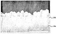
도 6은 본 발명의 일 실시예에 따른 전류 스프레딩층의 주사전자현미경(SEM) 사진이다.
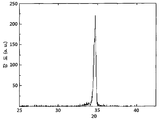
도 7은 본 발명의 일 실시예에 따른 전류 스프레딩층의 결정성을 나타내는 엑스선회절분석 그래프이다.
도 8은 본 발명의 열처리 온도에 따른 접촉 저항을 나타내는 그래프이다.
도 9는 발광소자의 전류-전압 곡선을 나타내는 그래프이다.
<도면의 주요부분에 대한 부호의 설명>
10: 베이스 기판 11: 제1형 반도체층
12: 활성층 13: 제2형 반도체층
14: 전류 스프레딩층 15: 제1 전극
본 발명은 다양한 변경을 가할 수 있고 여러 가지 실시예를 가질 수 있는바, 특정 실시예들을 도면에 예시하고 상세한 설명에 상세하게 설명하고자 한다. 그러나, 이는 본 발명을 특정한 실시 형태에 대해 한정하려는 것이 아니며, 본 발명의 사상 및 기술 범위에 포함되는 모든 변경, 균등물 내지 대체물을 포함하는 것으로 이해되어야 한다.
이하, 첨부한 도면들을 참조하여, 본 발명의 바람직한 실시예를 보다 상세하게 설명하고자 한다. 이하, 도면상의 동일한 구성요소에 대해서는 동일한 참조부호를 사용하고 동일한 구성요소에 대해서 중복된 설명은 생략한다.
도 1 내지 도 5는 발광다이오드의 제조방법을 나타내는 개략도들로서, 발광 소자의 단위 셀에 한정되어 도시한다.
도 1을 참조하면, 베이스 기판(10) 상에 제1형 반도체층(11)을 형성한다. 상기 베이스 기판(10)은 Al2O3(사파이어), SiC, ZnO, Si, GaAs, LiAl2O3, InP, BN, AlN 또는 GaN 기판일 수 있다. 바람직하게는 상기 베이스 기판(10)은 Al2O3 기판일 수 있다.
상기 제1형 반도체층(11)은 제1형 불순물 예를 들어, n형 불순물이 주입된 질화물계 반도체층, 구체적으로는 질화갈륨계 반도체층일 수 있다. 상기 n형 질화갈륨계 반도체층은 GaN층 또는 AlxGa(1-x)N(0≤x≤1)층일 수 있다.
도 2를 참조하면, 상기 제1형 반도체층(11) 상에 활성층(12)을 형성할 수 있다. 상기 활성층(12)은 양자점 구조 또는 다중양자우물 구조(Multi Quantum Well Structure)를 가질 수 있다. 상기 활성층(12)이 다중양자우물 구조를 갖는 경우에, 상기 활성층(12)은 우물층으로서 InGaN층과 장벽층인 GaN층의 다중 구조를 가질 수 있다.
도 3을 참조하면, 상기 활성층(12) 상에 제2형 반도체층(13)을 위치시켜 발광구조체(S)를 형성할 수 있다. 상기 제2형 반도체층(13)은 제2형 불순물 예를 들어, p형 불순물이 주입된 질화물계 반도체층, 구체적으로는 질화갈륨계 반도체층일 수 있다. 상기 p형 질화갈륨계 반도체층은 GaN층 또는 AlxGa(1-x)N(0≤x≤1)층일 수 있다.
상기와 같이 제1형 반도체층(11), 상기 활성층(12) 및 상기 제2형 반도체층(13)은 MOCVD(Metal Organic Chemical Vapor Deposition) 기술 또는 MBE(Molecular Beam Epitaxy) 기술을 사용하여 형성할 수 있다.
도 4를 참조하면, 상기 발광구조체(S) 상부면에 산화아연계 박막 (14a) 및 상기 산화아연계 박막(14a) 상에 돌출된 산화아연계 나노 막대들(14b)을 구비하는 전류 스프레딩층(14)을 형성할 수 있다. 상기 전류 스프레딩층(14)은 MOCVD(Metal Organic Chemical Vapor Deposition) 성장법을 이용하여 형성할 수 있다. 상기 전류 스프레딩층(14)은 반응물질로서 1 내지 250㎛ol/min, 바람직하게는 15 내지 25㎛ol/min의 디에틸아연(zinc diethyl), 10 내지 80000sccm, 바람직하게는 7000 내지 8000sccm 산소(O2) 및 0.01 내지 1000㎚ol/min, 바람직하게는 3 내지 4㎚ol/min의 트리메틸갈륨(TMGa)을 사용하여 형성할 수 있다. 이때, 반응기 내의 압력은 0.001 내지 10000torr로 수행할 수 있으며, 바람직하게는 45 내지 55 torr, 더 바람직하게는 50 torr의 압력으로 수행할 수 있다. 온도는 100℃ 내지 1000℃, 바람직하게는 500℃ 내지 800℃의 온도로 수행할 수 있으며, 더 바람직하게는 650℃의 온도로 수행할 수 있다.
상기 산화 아연계 전류 스프레딩층(14)을 형성하는 과정에서, 상기 전류 스프레딩층(14)과 상기 제2형 반도체층(13), 일 예로서 질화갈륨층 사이의 격자 상수 차이에 의해 상기 제2형 반도체층(13)의 안정화된 부분에 산화 아연계 씨드들이 형성된다. 상기 씨드들은 서로 연결되어 사슬 모양 또는 망사 모양의 산화아연계 씨드층을 형성할 수 있다. 이 후, 인시츄(in-situ)로 성장을 계속 진행하면 상기 씨드들은 수평보다 수직 방향으로 우세한 성장을 나타내어, 돌출된 나노 막대 형상으로 성장될 수 있다. 이 때, 상기 수평 성장에 의해 상기 나노 막대들(14b)의 하부는 서로 연결되어 산화아연계 박막(14a)을 형성할 수 있다. 결과적으로, 전류 스프레딩층(14)은 산화아연계 박막(14a) 및 상기 산화아연계 박막(14a) 상에 돌출된 산화아연계 나노 막대들(14b)을 구비할 수 있다.
상기 산화아연계 박막(14a)은 상기 제2형 반도체층(13)에 전류가 효율적으로 주입되도록 면을 따라 전류를 공급하는 투명도전막의 역할을 수행할 수 있다. 상기 나노 막대들(14b)은 광결정층의 역할을 수행할 수 있다. 상기 나노 막대들(14b)을 구비하는 경우에 소자 내부에서 전반사에 의해 빛이 갇히는 현상을 방지하고, 광추출효율을 향상시킬 수 있다.
또한, 상기 전류 스프레딩층(14)의 전기적 특성을 향상시키기 위해 추가적으로 열처리를 수행할 수 있다. 상기 열처리는 50℃ 내지 1000℃의 온도로 수행될 수 있다. 바람직하게는 450℃ 내지 550℃의 온도로 수행될 수 있다. 구체적으로, 상기 열처리를 수행하기 전에 챔버 내부는 질소 가스로 충전될 수 있다. 상기 질소 가스는 발광 소자에 구비된 각각 층들의 산화를 방지할 수 있다. 상기 질소 가스는 1기압 이상으로 유지할 수 있다. 더불어 급격한 승온을 막기위해 승온 속도를 조절할 수 있다. 상기와 같이 승온 속도를 조절하여 이종 물질간의 열팽창 차이로 인한 균열을 방지할 수 있다. 상기 승온 속도는 30℃/1sec로 수행될 수 있다.
상기 열처리가 수행되면, 상기 제2형 반도체층(13)과 상기 전류 스프레딩층(14) 사이의 오믹콘택(ohmic contact) 특성이 향상될 수 있고, 구동 전압이 감소될 수 있다. 상기 전류 스프레딩층(14)은 상기 제2형 반도체층(13)의 상부면과 전기적으로 접속하면서, 상부 전극으로서의 역할을 할 수 있다.
도 5를 참조하면, 상기 전류 스프레딩층(14), 제2형 반도체층(13) 및 상기 활성층(12)의 일부를 식각하여 상기 제1형 반도체층(11)의 일부를 노출시킨다. 이 때, 상기 제1형 반도체층(11)의 상부 일부 또한 식각될 수도 있다. 이에 따라, 발광 다이오드는 차례로 적층된 상기 제1형 반도체층(11), 상기 활성층(12), 상기 제2형 반도체층(13) 및 전류 스프레딩층(14)을 구비하되, 상기 활성층(12), 상기 제2형 반도체층(13) 및 상기 전류 스프레딩층(14)의 일측에는 상기 제1형 반도체층(11)이 노출될 수 있다. 상기 노출된 제1형 반도체층(11)의 상부면 상에 전기적으로 접속하는 하부 전극(15)을 구비할 수 있다. 상기 하부 전극(15)은 Al 및/또는 Ag을 함유할 수 있다.
도 6은 본 발명의 일 실시예에 따른 전류 스프레딩층의 주사전자현미경(SEM) 사진이다.
도 6을 참조하면, 전류 스프레딩층(14)은 산화아연계 박막(14a)과 나노 막대들(14b)을 포함한다. 상기 산화아연계 박막(14a)은 사슬구조의 박막 형상을 나타내며, 상기 나노 막대들(14b)은 상기 산화아연계 박막(14a) 상에 돌출된 막대 형상으로 구비되는 것을 확인할 수 있다. 이와 같이 상기 산화아연계 박막(14a) 상에 나노 막대들(14b)이 구비되는 경우, 소자 내부에서 전반사에 의해 빛이 갇히는 현상을 방지하고, 광추출효율을 향상시킬 수 있다.
도 7은 본 발명의 일 실시예에 따른 전류 스프레딩층의 결정성을 나타내는 엑스선회절분석 그래프이다.
도 7을 참조하면, 전류 스프레딩층은 34°에서 하나의 피크만 도출되었다. 이는 전류 스프레딩층이 산화아연 단결정임을 나타낸다.
도 8은 본 발명의 열처리 온도에 따른 접촉 저항을 나타내는 그래프이다. 상기 접촉 저항은 C-TLM(Circular Transmission Line Model)방법을 이용하여 측정하였다. 열처리 온도에 따른 접촉 저항을 비교하기 위해, 열처리 전, 300℃ 및 500℃의 열처리 후 각각의 접촉 저항을 나타내었다.
도 8을 참조하면, 열처리를 수행하지 않는 경우, 접촉저항이 다소 높으며, 전압에 따른 전류의 변화가 크지 않았다. 300℃의 열처리 후에는 상기 열처리전에 비해 접촉저항이 다소 감소되어, 제2형 반도체층과 전류 스프레딩층 간의 오믹콘택특성이 다소 향상되었음을 알 수 있다. 또한, 500℃까지 열처리 하는 경우, 접촉저항이 현저하게 감소하며, 전류의 변화량이 크게 나타났다. 이는 제2형 반도체층과 전류 스프레딩층 간의 오믹콘택특성이 크게 향상되었음을 나타낼 수 있다. 이에 따라 소자의 구동전압이 감소될 수 있다. 상기 결과로부터 상기 열처리는 300℃ 내지 500℃로 수행할 수 있으며, 바람직하게는 500℃으로 수행할 수 있다.
도 9는 발광소자의 전류-전압 곡선을 나타내는 그래프이다. 구체적으로, 전류 스프레딩층을 산화아연으로 형성한 본 발명의 열처리 전과 후의 구동전압 및 전류 전류 스프레딩층을 ITO으로 형성한 기존 발명의 구동전압을 비교하였다. 이때, 상기 구동전압은 전류가 20mA에 도달했을 때를 측정하였으며, 본 발명은 500℃의 온도로 열처리를 수행하였다.
도 9를 참조하면, 기존 발명의 경우, 구동 전압은 3.6V로 나타났다. 본 발명의 경우, 열처리전의 구동전압은 4.0V로 나타났으며, 열처리후의 구동전압은 3.4V가 나타났다. 상기 결과를 통해 알 수 있는 바와 같이, 열처리를 수행하면 전기적특성이 향상되어 구동전압이 감소될 수 있으며, 본 발명에서 제조된 산화아연 발광소자는 기존에 사용된 TIO 발광소자에 비해 전기적 특성이 향상되는 것을 알 수 있다. 이는 산화아연에 맞는 열처리 조건 및 제조방법이 확립되었기 때문으로 판단된다.
상기에서는 본 발명의 바람직한 실시예를 참조하여 설명하였지만, 해당 기술 분야의 숙련된 당업자는 하기의 특허 청구의 범위에 기재된 본 발명의 사상 및 영역으로부터 벗어나지 않는 범위 내에서 본 발명을 다양하게 수정 및 변경시킬 수 있음을 이해할 수 있을 것이다.
Claims (8)
- 베이스 기판 상에 차례로 위치하는 제1형 반도체층, 활성층 및 제2형 반도체층을 구비하는 발광구조체; 및상기 발광구조체 상부면에 위치하며, 산화아연계 박막 및 상기 산화아연계 박막 상에 돌출된 산화아연계 나노 막대들을 구비하는 전류 스프레딩층을 포함하는 발광 다이오드.
- 제 1 항에 있어서,상기 제2형 반도체층은 질화갈륨계 반도체층인 발광 다이오드.
- 베이스 기판 상에 차례로 위치하는 제1형 반도체층, 활성층 및 제2형 반도체층을 구비하는 발광구조체를 형성하는 단계; 및상기 발광구조체의 상부면에 MOCVD 성장법을 이용하여 산화아연계 박막 및 상기 산화아연계 박막 상에 돌출된 산화아연계 나노 막대들을 구비하는 전류 스프레딩층을 형성하는 단계를 포함하는 발광 다이오드의 제조방법.
- 제 3 항에 있어서,상기 전류 스프레딩층은 0.01 내지 10000 torr의 기압에서 형성되는 발광 다이오드의 제조방법.
- 제 3 항에 있어서,상기 전류 스프레딩층은 100 내지 1000℃의 온도에서 형성되는 발광 다이오드의 제조방법.
- 제 3 항에 있어서,상기 전류 스프레딩층은 1 내지 250㎛ol/min 디에틸아연, 10 내지 80000sccm 산소 및 0.01 내지 1000㎚ol/min 트리메틸갈륨을 사용하여 형성되는 발광 다이오드의 제조방법.
- 제 3 항에 있어서,열처리 하는 단계를 더 포함하는 발광 다이오드의 제조방법.
- 제 7 항에 있어서,상기 열처리는 50℃ 내지 1000℃의 온도로 수행하는 발광 다이오드의 제조방법.
Applications Claiming Priority (2)
| Application Number | Priority Date | Filing Date | Title |
|---|---|---|---|
| KR10-2008-0093404 | 2008-09-23 | ||
| KR1020080093404A KR20100034334A (ko) | 2008-09-23 | 2008-09-23 | 산화 아연계 전극을 이용한 발광 다이오드 및 그의 제조방법 |
Publications (2)
| Publication Number | Publication Date |
|---|---|
| WO2010036030A2 true WO2010036030A2 (ko) | 2010-04-01 |
| WO2010036030A3 WO2010036030A3 (ko) | 2010-07-01 |
Family
ID=42060276
Family Applications (1)
| Application Number | Title | Priority Date | Filing Date |
|---|---|---|---|
| PCT/KR2009/005434 Ceased WO2010036030A2 (ko) | 2008-09-23 | 2009-09-23 | 산화 아연계 전극을 이용한 발광 다이오드 및 그의 제조방법 |
Country Status (2)
| Country | Link |
|---|---|
| KR (1) | KR20100034334A (ko) |
| WO (1) | WO2010036030A2 (ko) |
Cited By (1)
| Publication number | Priority date | Publication date | Assignee | Title |
|---|---|---|---|---|
| GB2469869A (en) * | 2009-05-01 | 2010-11-03 | Univ Bolton | Continuous ZnO films |
Family Cites Families (3)
| Publication number | Priority date | Publication date | Assignee | Title |
|---|---|---|---|---|
| KR100554155B1 (ko) * | 2003-06-09 | 2006-02-22 | 학교법인 포항공과대학교 | 금속/반도체 나노막대 이종구조를 이용한 전극 구조물 및그 제조 방법 |
| KR100621918B1 (ko) * | 2004-06-10 | 2006-09-14 | 학교법인 포항공과대학교 | 투명 전도성 나노막대를 전극으로 포함하는 발광소자 |
| KR20080030042A (ko) * | 2008-01-24 | 2008-04-03 | 서울옵토디바이스주식회사 | 질화물 다층 양자 웰을 가지는 나노막대 어레이 구조의발광 다이오드 |
-
2008
- 2008-09-23 KR KR1020080093404A patent/KR20100034334A/ko not_active Ceased
-
2009
- 2009-09-23 WO PCT/KR2009/005434 patent/WO2010036030A2/ko not_active Ceased
Cited By (1)
| Publication number | Priority date | Publication date | Assignee | Title |
|---|---|---|---|---|
| GB2469869A (en) * | 2009-05-01 | 2010-11-03 | Univ Bolton | Continuous ZnO films |
Also Published As
| Publication number | Publication date |
|---|---|
| WO2010036030A3 (ko) | 2010-07-01 |
| KR20100034334A (ko) | 2010-04-01 |
Similar Documents
| Publication | Publication Date | Title |
|---|---|---|
| CN104272477B (zh) | 氮化物半导体发光元件 | |
| US8829545B2 (en) | Group III nitride semiconductor light-emitting device | |
| CN106057988B (zh) | 一种GaN基发光二极管的外延片的制备方法 | |
| US11482642B2 (en) | Light emitting element | |
| WO2014168339A1 (ko) | 자외선 발광 소자 | |
| CN102005513A (zh) | 具有低温p型GaN层的氮化镓系发光二极管 | |
| US8049227B2 (en) | Group III nitride semiconductor light emitting device, method for producing the same, and lamp thereof | |
| WO2013100619A1 (ko) | 탄소 도핑된 p형 질화물층을 포함하는 질화물계 발광소자 | |
| US12402441B2 (en) | Semiconductor device | |
| US20160043272A1 (en) | Monolithic light-emitting device | |
| EP2174358B1 (en) | Semiconductor light emitting device and method of manufacturing the same | |
| TW202427823A (zh) | 半導體元件 | |
| CN201766093U (zh) | 一种氮化镓系发光二极管 | |
| CN101840969A (zh) | 一种具有提升光取出率的半导体光电元件及其制造方法 | |
| WO2013066088A1 (ko) | 투명 박막, 이를 포함하는 발광 소자와 이들의 제조 방법 | |
| WO2011034273A1 (ko) | 반도체 발광소자 | |
| WO2010036030A2 (ko) | 산화 아연계 전극을 이용한 발광 다이오드 및 그의 제조방법 | |
| KR100770440B1 (ko) | 질화물 반도체 발광소자 | |
| CN104952994A (zh) | 一种Al组分渐变式P型LED结构及制备方法 | |
| WO2013147453A1 (ko) | 질화갈륨계 발광 다이오드 | |
| KR100813602B1 (ko) | 질화물 반도체 발광소자의 제조방법 | |
| KR100891827B1 (ko) | 수직구조 질화물 반도체 발광 소자 및 제조방법 | |
| WO2017090903A1 (ko) | 매립된 p형 컨택층을 포함하는 발광다이오드 | |
| US9508895B2 (en) | Group III nitride semiconductor light-emitting device and production method therefor | |
| KR20080023980A (ko) | 질화물 반도체 발광소자 및 그 제조 방법 |
Legal Events
| Date | Code | Title | Description |
|---|---|---|---|
| 121 | Ep: the epo has been informed by wipo that ep was designated in this application |
Ref document number: 09816423 Country of ref document: EP Kind code of ref document: A2 |
|
| NENP | Non-entry into the national phase |
Ref country code: DE |
|
| 122 | Ep: pct application non-entry in european phase |
Ref document number: 09816423 Country of ref document: EP Kind code of ref document: A2 |