EP2174358B1 - Semiconductor light emitting device and method of manufacturing the same - Google Patents
Semiconductor light emitting device and method of manufacturing the same Download PDFInfo
- Publication number
- EP2174358B1 EP2174358B1 EP08792900.6A EP08792900A EP2174358B1 EP 2174358 B1 EP2174358 B1 EP 2174358B1 EP 08792900 A EP08792900 A EP 08792900A EP 2174358 B1 EP2174358 B1 EP 2174358B1
- Authority
- EP
- European Patent Office
- Prior art keywords
- layer
- semiconductor layer
- undoped
- ingan
- light emitting
- Prior art date
- Legal status (The legal status is an assumption and is not a legal conclusion. Google has not performed a legal analysis and makes no representation as to the accuracy of the status listed.)
- Active
Links
- 239000004065 semiconductor Substances 0.000 title claims description 248
- 238000004519 manufacturing process Methods 0.000 title claims description 9
- 238000000034 method Methods 0.000 claims description 37
- 230000008569 process Effects 0.000 claims description 27
- APFVFJFRJDLVQX-UHFFFAOYSA-N indium atom Chemical compound [In] APFVFJFRJDLVQX-UHFFFAOYSA-N 0.000 claims description 17
- 229910052738 indium Inorganic materials 0.000 claims description 16
- 230000004888 barrier function Effects 0.000 claims description 9
- 239000002019 doping agent Substances 0.000 claims description 8
- 230000007547 defect Effects 0.000 claims description 6
- 239000000969 carrier Substances 0.000 claims description 4
- 230000005669 field effect Effects 0.000 claims description 3
- 229910052736 halogen Inorganic materials 0.000 claims description 3
- 150000002367 halogens Chemical class 0.000 claims description 3
- QSHDDOUJBYECFT-UHFFFAOYSA-N mercury Chemical compound [Hg] QSHDDOUJBYECFT-UHFFFAOYSA-N 0.000 claims description 3
- 229910052753 mercury Inorganic materials 0.000 claims description 3
- 229910052751 metal Inorganic materials 0.000 claims description 3
- 239000002184 metal Substances 0.000 claims description 3
- 125000005842 heteroatom Chemical group 0.000 claims description 2
- 150000002500 ions Chemical class 0.000 claims 1
- 239000000758 substrate Substances 0.000 description 26
- 238000011065 in-situ storage Methods 0.000 description 10
- 239000000463 material Substances 0.000 description 7
- 239000013078 crystal Substances 0.000 description 5
- 229910002704 AlGaN Inorganic materials 0.000 description 4
- 229910019080 Mg-H Inorganic materials 0.000 description 4
- 150000004767 nitrides Chemical class 0.000 description 4
- 239000000126 substance Substances 0.000 description 4
- 239000012159 carrier gas Substances 0.000 description 3
- 238000005229 chemical vapour deposition Methods 0.000 description 3
- 238000005530 etching Methods 0.000 description 3
- 239000007789 gas Substances 0.000 description 3
- 230000001965 increasing effect Effects 0.000 description 3
- UFHFLCQGNIYNRP-UHFFFAOYSA-N Hydrogen Chemical compound [H][H] UFHFLCQGNIYNRP-UHFFFAOYSA-N 0.000 description 2
- 238000001311 chemical methods and process Methods 0.000 description 2
- 238000006243 chemical reaction Methods 0.000 description 2
- 150000001875 compounds Chemical class 0.000 description 2
- 230000000694 effects Effects 0.000 description 2
- 238000005401 electroluminescence Methods 0.000 description 2
- 230000012010 growth Effects 0.000 description 2
- 230000004048 modification Effects 0.000 description 2
- 238000012986 modification Methods 0.000 description 2
- 238000005240 physical vapour deposition Methods 0.000 description 2
- 238000005381 potential energy Methods 0.000 description 2
- IJGRMHOSHXDMSA-UHFFFAOYSA-N Atomic nitrogen Chemical compound N#N IJGRMHOSHXDMSA-UHFFFAOYSA-N 0.000 description 1
- 229910001218 Gallium arsenide Inorganic materials 0.000 description 1
- PNEYBMLMFCGWSK-UHFFFAOYSA-N aluminium oxide Inorganic materials [O-2].[O-2].[O-2].[Al+3].[Al+3] PNEYBMLMFCGWSK-UHFFFAOYSA-N 0.000 description 1
- 229910052788 barium Inorganic materials 0.000 description 1
- 229910052791 calcium Inorganic materials 0.000 description 1
- 229910052593 corundum Inorganic materials 0.000 description 1
- 238000000151 deposition Methods 0.000 description 1
- 230000008021 deposition Effects 0.000 description 1
- 230000006866 deterioration Effects 0.000 description 1
- 229910001873 dinitrogen Inorganic materials 0.000 description 1
- 238000010292 electrical insulation Methods 0.000 description 1
- 230000002708 enhancing effect Effects 0.000 description 1
- 230000007717 exclusion Effects 0.000 description 1
- 239000010408 film Substances 0.000 description 1
- 238000010438 heat treatment Methods 0.000 description 1
- 239000013067 intermediate product Substances 0.000 description 1
- 230000001678 irradiating effect Effects 0.000 description 1
- 229910052749 magnesium Inorganic materials 0.000 description 1
- 229910001425 magnesium ion Inorganic materials 0.000 description 1
- 239000012071 phase Substances 0.000 description 1
- 239000000047 product Substances 0.000 description 1
- 230000006798 recombination Effects 0.000 description 1
- 238000005215 recombination Methods 0.000 description 1
- 239000007790 solid phase Substances 0.000 description 1
- 230000007480 spreading Effects 0.000 description 1
- 238000003892 spreading Methods 0.000 description 1
- 238000004544 sputter deposition Methods 0.000 description 1
- 229910052712 strontium Inorganic materials 0.000 description 1
- 239000010409 thin film Substances 0.000 description 1
- 229910052718 tin Inorganic materials 0.000 description 1
- XCZXGTMEAKBVPV-UHFFFAOYSA-N trimethylgallium Chemical compound C[Ga](C)C XCZXGTMEAKBVPV-UHFFFAOYSA-N 0.000 description 1
- 238000001039 wet etching Methods 0.000 description 1
- 229910001845 yogo sapphire Inorganic materials 0.000 description 1
- 229910052725 zinc Inorganic materials 0.000 description 1
Images


Classifications
-
- H—ELECTRICITY
- H01—ELECTRIC ELEMENTS
- H01L—SEMICONDUCTOR DEVICES NOT COVERED BY CLASS H10
- H01L33/00—Semiconductor devices with at least one potential-jump barrier or surface barrier specially adapted for light emission; Processes or apparatus specially adapted for the manufacture or treatment thereof or of parts thereof; Details thereof
- H01L33/02—Semiconductor devices with at least one potential-jump barrier or surface barrier specially adapted for light emission; Processes or apparatus specially adapted for the manufacture or treatment thereof or of parts thereof; Details thereof characterised by the semiconductor bodies
- H01L33/025—Physical imperfections, e.g. particular concentration or distribution of impurities
-
- H—ELECTRICITY
- H01—ELECTRIC ELEMENTS
- H01L—SEMICONDUCTOR DEVICES NOT COVERED BY CLASS H10
- H01L21/00—Processes or apparatus adapted for the manufacture or treatment of semiconductor or solid state devices or of parts thereof
- H01L21/02—Manufacture or treatment of semiconductor devices or of parts thereof
- H01L21/02104—Forming layers
- H01L21/02365—Forming inorganic semiconducting materials on a substrate
- H01L21/02367—Substrates
- H01L21/0237—Materials
-
- H—ELECTRICITY
- H01—ELECTRIC ELEMENTS
- H01L—SEMICONDUCTOR DEVICES NOT COVERED BY CLASS H10
- H01L21/00—Processes or apparatus adapted for the manufacture or treatment of semiconductor or solid state devices or of parts thereof
- H01L21/02—Manufacture or treatment of semiconductor devices or of parts thereof
- H01L21/02104—Forming layers
- H01L21/02365—Forming inorganic semiconducting materials on a substrate
- H01L21/02436—Intermediate layers between substrates and deposited layers
- H01L21/02439—Materials
- H01L21/02455—Group 13/15 materials
- H01L21/02458—Nitrides
-
- H—ELECTRICITY
- H01—ELECTRIC ELEMENTS
- H01L—SEMICONDUCTOR DEVICES NOT COVERED BY CLASS H10
- H01L21/00—Processes or apparatus adapted for the manufacture or treatment of semiconductor or solid state devices or of parts thereof
- H01L21/02—Manufacture or treatment of semiconductor devices or of parts thereof
- H01L21/02104—Forming layers
- H01L21/02365—Forming inorganic semiconducting materials on a substrate
- H01L21/02518—Deposited layers
- H01L21/02521—Materials
- H01L21/02538—Group 13/15 materials
- H01L21/0254—Nitrides
-
- H—ELECTRICITY
- H01—ELECTRIC ELEMENTS
- H01L—SEMICONDUCTOR DEVICES NOT COVERED BY CLASS H10
- H01L21/00—Processes or apparatus adapted for the manufacture or treatment of semiconductor or solid state devices or of parts thereof
- H01L21/02—Manufacture or treatment of semiconductor devices or of parts thereof
- H01L21/02104—Forming layers
- H01L21/02365—Forming inorganic semiconducting materials on a substrate
- H01L21/02518—Deposited layers
- H01L21/0257—Doping during depositing
- H01L21/02573—Conductivity type
-
- H—ELECTRICITY
- H01—ELECTRIC ELEMENTS
- H01L—SEMICONDUCTOR DEVICES NOT COVERED BY CLASS H10
- H01L21/00—Processes or apparatus adapted for the manufacture or treatment of semiconductor or solid state devices or of parts thereof
- H01L21/02—Manufacture or treatment of semiconductor devices or of parts thereof
- H01L21/02104—Forming layers
- H01L21/02365—Forming inorganic semiconducting materials on a substrate
- H01L21/02612—Formation types
- H01L21/02617—Deposition types
- H01L21/0262—Reduction or decomposition of gaseous compounds, e.g. CVD
-
- H—ELECTRICITY
- H01—ELECTRIC ELEMENTS
- H01L—SEMICONDUCTOR DEVICES NOT COVERED BY CLASS H10
- H01L33/00—Semiconductor devices with at least one potential-jump barrier or surface barrier specially adapted for light emission; Processes or apparatus specially adapted for the manufacture or treatment thereof or of parts thereof; Details thereof
- H01L33/005—Processes
- H01L33/0062—Processes for devices with an active region comprising only III-V compounds
- H01L33/0075—Processes for devices with an active region comprising only III-V compounds comprising nitride compounds
Definitions
- Embodiments relate to a semiconductor light emitting device and a method of manufacturing the same.
- a group III-V nitride semiconductor is being spotlighted as a gist material of a light emitting device such as a light emitting diode (LED) or a laser diode (LD) due to its physical and chemical properties.
- a light emitting device such as a light emitting diode (LED) or a laser diode (LD) due to its physical and chemical properties.
- LED light emitting diode
- LD laser diode
- the group III-V nitride semiconductors are being widely used for light emitting devices that emit light having a blue or green wavelength band and applied as light sources of a variety of products such as high-speed swindling devices such as metal semiconductor field effect transistors (MESFET) and hetero junction field effect transistors (HEMT), high-output devices, keypad light emitting units of mobile phones, electronic scoreboards, and lightings.
- high-speed swindling devices such as metal semiconductor field effect transistors (MESFET) and hetero junction field effect transistors (HEMT), high-output devices, keypad light emitting units of mobile phones, electronic scoreboards, and lightings.
- Embodiments provide a semiconductor light emitting device that can generate minority carriers in at least one semiconductor layer using a lighting source and a method of manufacturing the semiconductor light emitting device.
- Embodiments provide a semiconductor light emitting device that can expose an undoped semiconductor layer to light from a lighting source and a method of manufacturing the semiconductor light emitting device.
- Embodiments provide a semiconductor light emitting device that can expose an InGaN layer comprising low-mol indium between a first conductive semiconductor layer and an active layer to light from a lighting source and a method of manufacturing the semiconductor light emitting device.
- Embodiments provide a semiconductor light emitting device that can generate minority holes by exposing a quantum well layer of an active layer to light from a lighting source and a method of manufacturing the semiconductor light emitting device.
- Embodiments provide a semiconductor light emitting device that can generate minority electrons by exposing a second conductive semiconductor layer on an active layer to light from a lighting source.
- An embodiment provides a semiconductor device as defined in claim 1.
- Embodiments of the semiconductor device are further defined in claims 2-7.
- An embodiment provides a method of manufacturing a semiconductor light emitting device as defined in claim 8. Embodiments of the method are further defined in claims 9-15.
- the embodiments can improve light emission efficiency of an active layer.
- the embodiments can enhance electrical tolerance such as ESD and improve a diode electrical property such as an inverse current, an inverse voltage, and the light of a semiconductor light emitting device.
- the embodiments can provide a first conductive semiconductor layer that has an excellent crystallinity.
- Figs. 1 to 4 illustrate a first embodiment.
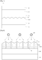
- Fig. 1 is a side sectional view of a semiconductor device according to a first embodiment
- Fig. 2 is a view of an example of forming an undoped semiconductor layer of Fig. 1 .
- a semiconductor device 100 comprises a substrate 110, a buffer layer 120, a first undoped semiconductor layer 130A, a first conductive semiconductor layer 140, an active layer 150, and a second conductive semiconductor layer 160.
- the substrate 110 may be formed of at least one of Al 2 O 3 , GaN, SiC, ZnO, Si, GaP, InP, Ge, and GaAs.
- the substrate 110 may be a substrate having a conductive property.
- the surface of the substrate 110 may be provided with a pattern having protrusions and grooves.
- the substrate 110 is not limited thereto.
- a nitride semiconductor is grown on the substrate 110.
- a physical vapor deposition (PVD) apparatus a chemical vapor deposition (CVD) apparatus, a plasma laser deposition (PLD) apparatus, a dual-type thermal evaporator sputtering apparatus, a metal organic chemical vapor deposition apparatus may be used as a growing apparatus.
- PVD physical vapor deposition
- CVD chemical vapor deposition
- PLD plasma laser deposition
- dual-type thermal evaporator sputtering apparatus a metal organic chemical vapor deposition apparatus
- the buffer layer 120 is formed on the substrate 110.
- the buffer layer 120 may be formed of GaN, InN, AlN, AlInN, InGaN, AlGaN, InAlGaN, or the like.
- the buffer layer 120 attenuates lattice mismatch between GaN and a material of the substrate 110.
- the buffer layer 120 may be not formed.
- the first undoped semiconductor layer 130A is formed on the buffer layer 120.
- the first undoped semiconductor layer 130A may be an undoped GaN layer and functions as a substrate on which the nitride semiconductor is grown.
- the first undoped semiconductor layer 130A is grown in-situ by an exposure process using a lighting source 190 (for example, a lamp, hereinafter referred to as "lamp").
- a lighting source 190 for example, a lamp, hereinafter referred to as "lamp”
- the lamps 190 form photo electro luminescence growing.
- the lamp 190 may be selected from the group consisting of a mercury lamp, an X-ray lamp, an E-beam lamp, and a halogen lamp, and a combination thereof.
- the first undoped semiconductor layer 130A is formed to have a predetermined thickness (e.g., 1-5 ⁇ m) by supplying NH 3 and TMGa at a growing temperature (e.g., 700-1500°C).
- the first undoped semiconductor layer 130A is grown in-situ through an exposure process using the lamps 190.
- the first undoped semiconductor layer 130A is grown by the exposure process using the lamps 190, photo enhanced minority holes (Hm) are generated in the crystal of the first undoped semiconductor layer 130A.
- Hm photo enhanced minority holes
- dislocations Dt having positive charges are generated in the first undoped semiconductor layer 130A.
- a region 132 where the photo enhanced minority holes do not exist is formed around the dislocations Dt.
- a chemical equation for generating the undoped GaN layer is as follows: (CH 3 )3Ga(g) + NH 3 (g) ⁇ GaN(s) + 3CH 4 (g) where, (g) means a gas-phase and (s) means a solid-phase.
- peripheries of the dislocations Dt are normally grown at a normal growing rate of 2 ⁇ m/hr. Regions except for the peripheries of the dislocations Dt are grown at a relatively low growing rate lower than the normal growing rate by 10-15% since the generation of intermediate products such as holes (+) or electrons (-) that are generated by the above chemical equation is disturbed.
- a surface of the first undoped GaN layer 130A is uneven, i.e. has protrusions and grooves.
- the first undoped semiconductor layer 130A may be formed such that a dead zone 132 where the dislocations are generated is thicker than a zone where no dislocation exists.
- the dislocations having a bad effect on a LED structural property may be pinned and an area of the free surface increases.
- the first conductive semiconductor layer 140 is formed on the first undoped semiconductor layer 130A.
- the first conductive semiconductor layer 140 may be an N-type semiconductor layer doped with N-type dopants.
- the N-type semiconductor layer may be formed of a compound semiconductor selected from the group consisting of GaN, InN, AlN, InGaN, AlGaN, InAlGaN, AlInN.
- the N-type dopants comprise at least one of Si, Ge, Sn, and Te. Since the first conductive semiconductor layer 140 is formed on the first undoped semiconductor layer 130A, the crystal defects may be reduced.
- the active layer 150 is formed on the first conductive semiconductor layer 140.
- the active layer 150 may be formed in a single quantum well structure having an In x Ga 1-x N well layer/GaN barrier layer or a cycle of the In x Ga 1-x N well layer/Al y Ga 1-y N barrier layer or a multi-quantum well structure.
- the In x Ga 1-x N well layer and Al y Ga 1-y N barrier layer may be adjusted within a range of 0 ⁇ x ⁇ 1, 0 ⁇ y ⁇ 1.
- the semiconductor material for the active layer 150 may be varied in accordance with a wavelength of the light emitted. That is, the semiconductor material for the active layer 150 is not specifically limited.
- the second conductive semiconductor layer 160 is formed on the active layer 150.
- the second conductive semiconductor layer 160 may be a P-type semiconductor layer doped with P-type dopants.
- the P-type semiconductor layer may be formed of a compound semiconductor selected from the group consisting of GaN, InN, AlN, InGaN, AlGaN, InAlGaN, and AlInN.
- the P-type dopants comprise at least one of Mg, Zn, Ca, Sr, and Ba.
- a third conductive semiconductor layer (not shown) may be formed on the second conductive semiconductor layer 160.
- the third conductive semiconductor layer may be an N-type semiconductor layer.
- the semiconductor device 100 may be formed in one of an N-P junction structure, a P-N junction structure, an N-P-N junction structure, and a P-N-P junction structure.
- a structure comprising at least the first conductive semiconductor layer 140, the active layer 150, and the second conductive semiconductor layer 160 may be defined as a light emitting structure.
- the light emitting structure may comprise a semiconductor layer emitting electrons, a semiconductor layer emitting holes, and an active layer. Other layers may be further formed on or under the semiconductor layers. However, the light emitting structure is not limited to this configuration.
- the surface 131 of the first undoped semiconductor layer 130A may be formed to be uneven. Therefore, the crystal defects of the first conductive semiconductor layer 140 grown on the first undoped semiconductor layer 130A are reduced and thus the first conductive semiconductor layer 140 may have an excellent crystallinity. Further, the light emitting efficiency of the active layer 150 can be improved and diode properties such as the inverse current, inverse voltage, and the like of the resulting LED structure can be improved. Furthermore, an electrical tolerance such as electrostatic discharge (ESD) can be enhanced.
- ESD electrostatic discharge
- the first undoped semiconductor layer 130A is grown in-situ through the exposure process using the lamps 190
- the first conductive semiconductor layer 140 may be also grown in-situ through the exposure process using the lamps 190.
- At least one of the semiconductor layers 140, 150, and 160 on the first undoped semiconductor layer 130A may be grown in-situ through the exposure process using the lamps 190.
- the photo enhanced minority carriers such as electrons and holes are generated in the layer exposed to the light from the lamps 190 by the chemical reaction with materials injected during the growing process. Therefore, the light emitting efficiency and electrical tolerance of the active layer 150 can be enhanced.
- Fig. 3 is a side sectional view of a horizontal semiconductor light emitting device prepared using an embodiment as shown in Fig. 1 .
- the first conductive semiconductor layer 140 is exposed through a mesa etching process.
- a first electrode 181 is formed on a portion of the first conductive semiconductor layer 140 and a second electrode 183 is formed on the second conductive semiconductor layer 160.
- Fig. 4 is a side sectional view of a vertical semiconductor light emitting device prepared using an embodiment as shown in Fig. 1 .
- a reflective electrode layer 170 is formed on the second conductive semiconductor layer 160 and a conductive supporting substrate 175 is formed on the reflective electrode layer 170.
- the substrate 110 of Fig. 1 is removed through a physical or/and chemical process.
- a laser lift off (LLO) process that can remove the substrate 110 by irradiating laser having a predetermined wavelength to the substrate 110 may be used as the physical process.
- wet etching solution is injected to the buffer layer 120 or/and the first undoped semiconductor layer 130A between the substrate 110 and the first conductive semiconductor layer 140 to remove the buffer layer 120 or/and the first undoped semiconductor layer 130A and thus the substrate 110 is removed.
- a first electrode 181 may be formed under the first conductive semiconductor layer 140.
- an undersurface of the first conductive semiconductor layer 140 may be uneven to correspond to the uneven surface of the first undoped semiconductor layer 130A.
- Figs. 5 to 8 illustrate a second embodiment.
- Fig. 5 is a side sectional view of a semiconductor device according to a second embodiment
- Fig. 6 is a view of an example of forming a quantum well layer of an active layer of Fig. 5 .
- like reference numbers will be used to refer to like parts. The same parts as those of the first embodiment will not be described in this embodiment.
- a semiconductor device 101 comprises an active layer 150A exposed to light from lamps 192.
- the active layer 150A comprises a single quantum well structure or a multi-quantum well structure.
- the first undoped semiconductor layer 130 or/and the buffer layer 120 of the first embodiment may be not formed.
- an In x Ga 1-x N (0 ⁇ x ⁇ 1) quantum well layer 152 and a quantum barrier layer 154 are grown to form the active layer 150A.
- the quantum well layer 152 may be formed of InGaN and the quantum barrier layer 154 may be formed of GaN or AlGaN.
- the quantum well layer 152 When the quantum well layer 152 is grown, a large amount of Ga vacancies are generated. The Ga vacancies have negative charges to trap holes.
- the quantum well layer 152 is grown in-situ through an exposure process using the lamps 192. Photo enhanced minority holes are generated in the quantum well layer 152 and trapped in the vacancies. Therefore, the quantum well layer 152 effectively prevents the generation of the Ga vacancies in the InGaN having the negative charges. That is, the Ga vacancies are neutralized by the photo enhanced minority holes generated in the InGaN of the quantum well layer 152 and thus the trapping of the holes in the Ga vacancies is prevented, contributing to the emission of the light.
- Fig. 7 is a side sectional view of a horizontal semiconductor light emitting device prepared using an embodiment as shown in Fig. 5 .
- a first electrode 181 is formed on the first conductive semiconductor layer 140 and a second electrode 183 is formed on the second conductive semiconductor layer 160.
- the active layer 150A emits light by the combination of the electrons and holes.
- the free holes increase, thereby improving the light emitting efficiency.
- Fig. 8 is a side sectional view of a vertical semiconductor light emitting device prepared using an embodiment as shown in Fig. 5 .
- a reflective electrode layer 170 and a conductive supporting substrate 175 are formed on a second conductive semiconductor layer 160.
- the first undoped semiconductor layer 130, buffer layer 120, and substrate 110 that are shown in Fig. 5 and disposed under the first conductive semiconductor layer 140 are removed and the first electrode 181 is formed under the first conductive semiconductor layer 140.
- the free holes of the active layer 150A increase and thus the light emitting efficiency can be improved.
- Figs. 9 to 13 illustrate a third embodiment.
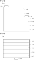
- Fig. 9 is a side sectional view of a semiconductor light emitting device according to a third embodiment
- Fig. 10 is a view of an example of a V-defect of a low-mol InGaN layer in Fig. 9
- Fig. 11 is a view of an example of forming a low-mol InGaN layer of Fig. 9 .
- like reference numbers will be used to refer to like parts. The same parts as those of the first embodiment will not be described in this embodiment.
- a semiconductor device 102 comprises a low-mol InGaN layer 145 having a small amount of indium.
- the low-mol InGaN layer 145 is formed between the first conductive semiconductor layer 140 and the active layer 150 and increases internal quantum efficiency of the active layer 150.
- the low-mol InGaN layer 145 may be grown to an InGaN spreading layer having a small amount of indium or an InGaN barrier layer to control a strain of the active layer 150.
- an amount of the indium doped may be less than 5% of an amount of the InGaN.
- the first undoped semiconductor layer 130 or/and the buffer layer 120 between the first conductive semiconductor layer 140 and the substrate 110 may be omitted.
- the indium when the indium is incorporated in the low-mol InGaN layer 145, the indium atoms are located on a (10 1 1) facet rather than a (0001) facet. Therefore, when the low-mol InGaN layer 145 contains the indium, a large amount of V-defect 147 may be generated.
- a surface 146 of the layer containing the indium has a predetermined surface energy E. When the V-defect 147 is generated, the surface energy E is altered to a surface energy E'.
- the V-defect 147 is continuously generated and increased until the surface 146 of the low-mol InGaN layer 145 has a minimum E' value.
- the (1011) facet is primarily grown than the (0001) facet 146 by the potential energy different (e.g., 1.5-2V).
- the low-mol InGaN layer 145 is exposed to the light from the lamps 194 in-situ. At this point, when the low-mol InGaN layer 145 is grown, the generation and growing of the V-defect 147 by the indium doping is suppressed and thus the high quality InGaN layer can be grown.
- the low-mol InGaN layer 145 when the low-mol InGaN layer 145 is exposed to the light from the lamps 194 during being grown, photo enhanced minority holes are generated in the crystal of the low-mol InGaN layer 145.
- the photo enhanced minority holes disturb a surface electric state of the (10 1 1) facet to suppress the generation and growing of the V-defect 147 caused by the indium. That is, the generated photo enhanced minority holes disturb a potential energy for the (10 1 1) facet of the V-defect 147 in the low-mol InGaN layer 145 to disturb the indium that intends to keep adhering to the V-defect 147, thereby suppressing the growing of the V-defect 147.
- the low-mol InGaN layer 145 is grown by exposure process using the lamps 194, the generation and growing of the V-defect 147 generated by the doping of the indium is suppressed, thereby growing a high quality InGaN layer 145.
- the active layer 150 grown on the low-mol InGaN layer 145 is improved in its light emitting efficiency and the diode property such as the inverse current and inverse voltage of the resulting LED structure is improved, thereby enhancing the electrical tolerance of the ESD and the like.
- Fig. 12 is a side sectional view of a horizontal semiconductor light emitting device prepared using an embodiment as shown in Fig. 9 .
- a horizontal semiconductor light emitting device 102A comprises a first conductive semiconductor layer 140, a low-mol InGaN layer 145, an active layer 150, and a second conductive semiconductor layer 160.
- the first conductive semiconductor layer 140 is exposed by a mesa etching process, the first electrode 181 is formed on the first conductive semiconductor layer 140 and the second electrode 183 is formed on the second conductive semiconductor layer 160.
- Fig. 13 is a side sectional view of a vertical semiconductor light emitting device prepared using an embodiment as shown in Fig. 9 .
- the first electrode 181 is formed under the first conductive semiconductor layer 140 and the low-mol InGaN layer 145, active layer 150, second conductive semiconductor layer 160, reflective electrode layer 170, and conductive supporting substrate 175 are sequentially formed on the first conductive semiconductor layer 140.
- the low-mol InGaN layer 145 having a small amount of indium is formed under the active layer 150, the low-mol InGaN layer 145 is exposed to the light from the lamps 194 (see Fig. 11 ) to suppress the generation and growing of the V-defect caused when the indium is doped, thereby improving the light emitting efficiency of the active layer 150.
- Figs. 14 to 17 illustrate a fourth embodiment.
- Fig. 14 is a side sectional view of a semiconductor device according to a fourth embodiment
- Fig. 15 is a view of a lamp exposure example of a second conductive semiconductor layer of Fig. 14 .
- like reference numbers will be used to refer to like parts. The same parts as those of the first embodiment will not be described in this embodiment.
- a semiconductor device 103 comprises a substrate 110, a buffer layer 120, a first undoped semiconductor layer 130, a first conductive semiconductor layer 140, an active layer 150, a second undoped semiconductor layer 155, and a second conductive semiconductor layer 160A.
- the first undoped semiconductor layer 130 is an undoped GaN layer, which may be exposed to light from the lamp. At least one of the buffer layer 120 and the first undoped semiconductor layer 130 may be omitted.
- the second undoped semiconductor layer 155 is grown on the active layer 150 and the second conductive semiconductor layer 160A is grown on the second undoped semiconductor layer 155.
- the second undoped semiconductor layer 155 may be an undoped GaN layer.
- a third undoped GaN layer may be formed on the second conductive semiconductor layer 160A.
- the second conductive semiconductor layer 160A is formed on the second undoped semiconductor layer 155.
- the second conductive semiconductor layer 160A is a P-type semiconductor layer, i.e., a P-type GaN layer, which is formed by supplying carrier gas such as hydrogen gas, and TMGa, (EtCp 2 Mg) ⁇ Mg(C 2 H 5 C 5 H 4 ) 2 ⁇ , and NH 3 at a predetermined growing temperature.
- a thickness of the second undoped semiconductor layer 155 is 1-50 nm (10-500 ⁇ ) and a thickness of the second conductive semiconductor layer 160A is 1-200 nm (10-2000 ⁇ ).
- the second conductive semiconductor layer 160A is grown as a thin film. Since the P-type dopants doped in the second conductive semiconductor layer 160A are naturally diffused to the second undoped semiconductor layer 155, the second conductive semiconductor layer 160A may be formed as the high quality semiconductor layer.
- the P-type dopants may be Mg but not be limited to this.
- the photo enhanced minority holes are generated in the second undoped semiconductor layer 155 and thus the combination between the photo enhanced minority holes and the H-ions may be induced. That is, the photo enhanced minority holes disturbs the Mg-H bond to improve the concentration of the hole-carrier.
- the second conductive semiconductor layer 160A when the second conductive semiconductor layer 160A is doped with Mg, the Mg is bonded to H of NH 3 to form Mg-H bond having an electrical insulation property. Therefore, it is difficult to attain a high concentration second conductive semiconductor layer 160A.
- the second conductive semiconductor layer 160A when the second conductive semiconductor layer 160A is grown in-situ through the exposure process using the lamps 196, the photo enhanced minority electrons are generated and the generated photo enhanced minority electrons are bonded to the Mg. Accordingly, the bonding of the Mg to the H-ions that are used as atmospheric gas and carrier gas is prevented and thus the deterioration of the Hole-carrier concentration of the second conductive semiconductor layer 160 can be prevented.
- the primary bond between the generated photo enhanced minority electrons and the Mg-ions are generated to prevent the Mg-H bond and increases the hole concentration through a heat treatment at a high temperature for a short time to the exclusion of the NH 3 and H 2 gases. Therefore, the damage of the active layer 150 is reduced, thereby improving the light emitting efficiency.
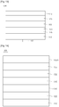
- Fig. 16 is a side sectional view of a horizontal semiconductor light emitting device prepared using an embodiment as shown in Fig. 14 .
- a horizontal semiconductor light emitting device 103A comprises a first conductive semiconductor layer 140, an active layer 150, a second undoped semiconductor layer 155, and a second conductive semiconductor layer 160A.
- a first electrode 181 is formed on the first conductive semiconductor layer 140 and a second electrode 183 is formed on the second conductive semiconductor layer 160A.
- Fig. 17 is a side sectional view of a vertical semiconductor light emitting device prepared using an embodiment as shown in Fig. 14 .
- a first electrode 181 is formed under a first conductive semiconductor layer 140, and an active layer 150, a second undoped semiconductor layer 155, a second conductive semiconductor layer 160A, a reflective electrode layer 170, and a conductive supporting substrate 175 are sequentially formed on the first conductive semiconductor layer 140.
- the second conductive semiconductor layer 160A when the second undoped semiconductor layer 155 and the second conductive semiconductor layer 160A are grown on the active layer 150, the second conductive semiconductor layer 160A is exposed to light from the lamps to form photo enhanced minority electrons. Therefore, the Mg-H bond is prevented in the second conductive semiconductor layer 160A and the hole concentration can be improved. In addition, since an amount of P-type dopants can be reduced and thus the damage of the active layer 150 can be reduced.
- the semiconductor devices 100, 101, 102, and 103 when growing the semiconductor devices 100, 101, 102, and 103 in accordance with the first to fourth embodiments, at least one of the semiconductor layers is grown in-situ through an exposure process using lamps. At this point, the semiconductor layer exposed to the light from the lamps generates photo enhanced minority carriers such as electrons and holes through a chemical reaction with materials implanted during the growing process. Therefore, the light emitting efficiency or electrical tolerance can be enhanced.
- the lamps disclosed in the embodiments are lamps for performing the photo electro luminescence growing.
- the lamps may be mercury lamps, X-ray lamps, E-beam lamps, and halogen lamps, and combination thereof.
- the lamps are not limited to these.
- different or same lamps may be used for different semiconductor layers.
- first undoped semiconductor layer of the first embodiment the active layer of the second embodiment, the low-mol InGaN layer of the third embodiment, and the second undoped semiconductor layer and the second conductive semiconductor layer of the fourth embodiment can be selectively applied to other embodiments.
- the exposing time of the semiconductor layers to the light from the lamps may be proportional to, greater than, or less than the growing time of the corresponding semiconductor layers.
- the embodiments can improve light emission efficiency of an active layer.
- the embodiments can improve a diode electrical property such as an inverse current, an inverse voltage, and the light of a semiconductor light emitting device.
- the embodiments can enhance an electrical tolerance such as ESD.
- the Embodiments can provide a first conductive semiconductor layer that has an excellent crystallinity.
Description
- Embodiments relate to a semiconductor light emitting device and a method of manufacturing the same.
- A group III-V nitride semiconductor is being spotlighted as a gist material of a light emitting device such as a light emitting diode (LED) or a laser diode (LD) due to its physical and chemical properties.
- The group III-V nitride semiconductors are being widely used for light emitting devices that emit light having a blue or green wavelength band and applied as light sources of a variety of products such as high-speed swindling devices such as metal semiconductor field effect transistors (MESFET) and hetero junction field effect transistors (HEMT), high-output devices, keypad light emitting units of mobile phones, electronic scoreboards, and lightings.
- Documents
US 4843031 ,EP 637086 A2 EP 1391941 A1 andJPH 5235408 - Documents
EP 1071143 A1 andUS 6015979 show the growths of GaN layers of a patterned substrate. - Embodiments provide a semiconductor light emitting device that can generate minority carriers in at least one semiconductor layer using a lighting source and a method of manufacturing the semiconductor light emitting device.
- Embodiments provide a semiconductor light emitting device that can expose an undoped semiconductor layer to light from a lighting source and a method of manufacturing the semiconductor light emitting device.
- Embodiments provide a semiconductor light emitting device that can expose an InGaN layer comprising low-mol indium between a first conductive semiconductor layer and an active layer to light from a lighting source and a method of manufacturing the semiconductor light emitting device.
- Embodiments provide a semiconductor light emitting device that can generate minority holes by exposing a quantum well layer of an active layer to light from a lighting source and a method of manufacturing the semiconductor light emitting device.
- Embodiments provide a semiconductor light emitting device that can generate minority electrons by exposing a second conductive semiconductor layer on an active layer to light from a lighting source.
- An embodiment provides a semiconductor device as defined in
claim 1. - Embodiments of the semiconductor device are further defined in claims 2-7.
- An embodiment provides a method of manufacturing a semiconductor light emitting device as defined in claim 8. Embodiments of the method are further defined in claims 9-15.
- The embodiments can improve light emission efficiency of an active layer.
- The embodiments can enhance electrical tolerance such as ESD and improve a diode electrical property such as an inverse current, an inverse voltage, and the light of a semiconductor light emitting device.
- The embodiments can provide a first conductive semiconductor layer that has an excellent crystallinity.
-
-
Fig. 1 is a side sectional view of a semiconductor device according to a first embodiment. -
Fig. 2 is a view of an example of forming an undoped semiconductor layer belonging to a semiconductor device as shown inFig. 1 . -
Fig. 3 is a side sectional view of a horizontal semiconductor light emitting device prepared using an embodiment as shown inFig. 1 . -
Fig. 4 is a side sectional view of a vertical semiconductor light emitting device prepared using an embodiment as shown inFig. 1 . -
Fig. 5 is a side sectional view of a semiconductor device according to a second embodiment. -
Fig. 6 is a view of a forming example of a quantum well layer of an active layer belonging to a semiconductor device as shown inFig. 5 . -
Fig. 7 is a side sectional view of a horizontal semiconductor light emitting device prepared using an embodiment as shown inFig. 5 . -
Fig. 8 is a side sectional view of a vertical semiconductor light emitting device prepared using an embodiment as shown inFig. 5 . -
Fig. 9 is a side sectional view of a semiconductor device according to a third embodiment. -
Fig. 10 is a view of an example of a V-defect of a low-mol InGaN layer belonging to a semiconductor device as shown inFig. 9 . -
Fig. 11 is a view of a forming example of a low-mol InGaN layer belonging to a semiconductor light emitting device as shown inFig. 9 . -
Fig. 12 is a side sectional view of a horizontal semiconductor light emitting device prepared using an embodiment as shown inFig. 9 . -
Fig. 13 is a side sectional view of a vertical semiconductor light emitting device prepared using an embodiment as shown inFig. 9 . -
Fig. 14 is a side sectional view of a semiconductor device according to a fourth embodiment. -
Fig. 15 is a view of a lamp exposure example of a second conductive semiconductor layer belonging to a semiconductor device as shown inFig. 14 . -
Fig. 16 is a side sectional view of a horizontal semiconductor light emitting device prepared using an embodiment as shown inFig. 14 . -
Fig. 17 is a side sectional view of a vertical semiconductor light emitting device prepared using an embodiment as shown inFig. 14 . - Hereinafter, semiconductor light emitting devices and methods of manufacturing the same in accordance with embodiments will be described with reference to the accompanying drawings. In the following description, it will be understood that when a layer (or film) is referred to as being "on" another layer or substrate, it can be directly on the other layer or substrate, or intervening layers may also be present. Further, it will be understood that when a layer is referred to as being "under" another layer, it can be directly under the other layer, and one or more intervening layers may also be present. In addition, "on" and "under" of each layer will be referred based on the drawings. Further, the thickness of each layer is exemplarily illustrated and thus the actual thickness of each layer is not limited to the drawings.
-
Figs. 1 to 4 illustrate a first embodiment. -
Fig. 1 is a side sectional view of a semiconductor device according to a first embodiment, andFig. 2 is a view of an example of forming an undoped semiconductor layer ofFig. 1 . - Referring to
Fig. 1 , asemiconductor device 100 comprises asubstrate 110, abuffer layer 120, a firstundoped semiconductor layer 130A, a firstconductive semiconductor layer 140, anactive layer 150, and a secondconductive semiconductor layer 160. - The
substrate 110 may be formed of at least one of Al2O3, GaN, SiC, ZnO, Si, GaP, InP, Ge, and GaAs. Thesubstrate 110 may be a substrate having a conductive property. The surface of thesubstrate 110 may be provided with a pattern having protrusions and grooves. However, thesubstrate 110 is not limited thereto. - A nitride semiconductor is grown on the
substrate 110. One of a physical vapor deposition (PVD) apparatus, a chemical vapor deposition (CVD) apparatus, a plasma laser deposition (PLD) apparatus, a dual-type thermal evaporator sputtering apparatus, a metal organic chemical vapor deposition apparatus may be used as a growing apparatus. - The
buffer layer 120 is formed on thesubstrate 110. Thebuffer layer 120 may be formed of GaN, InN, AlN, AlInN, InGaN, AlGaN, InAlGaN, or the like. Thebuffer layer 120 attenuates lattice mismatch between GaN and a material of thesubstrate 110. Here, thebuffer layer 120 may be not formed. - The first
undoped semiconductor layer 130A is formed on thebuffer layer 120. The firstundoped semiconductor layer 130A may be an undoped GaN layer and functions as a substrate on which the nitride semiconductor is grown. - Referring to
Figs. 1 and 2 , the firstundoped semiconductor layer 130A is grown in-situ by an exposure process using a lighting source 190 (for example, a lamp, hereinafter referred to as "lamp"). Here, thelamps 190 form photo electro luminescence growing. For example, thelamp 190 may be selected from the group consisting of a mercury lamp, an X-ray lamp, an E-beam lamp, and a halogen lamp, and a combination thereof. - The first
undoped semiconductor layer 130A is formed to have a predetermined thickness (e.g., 1-5 µm) by supplying NH3 and TMGa at a growing temperature (e.g., 700-1500°C). The firstundoped semiconductor layer 130A is grown in-situ through an exposure process using thelamps 190. - As the first
undoped semiconductor layer 130A is grown by the exposure process using thelamps 190, photo enhanced minority holes (Hm) are generated in the crystal of the firstundoped semiconductor layer 130A. Here, due to the mismatch between thesubstrate 110 and the GaN layer crystal, dislocations Dt having positive charges are generated in the firstundoped semiconductor layer 130A. In addition, aregion 132 where the photo enhanced minority holes do not exist is formed around the dislocations Dt. - A chemical equation for generating the undoped GaN layer is as follows:
(CH3)3Ga(g) + NH3(g) → GaN(s) + 3CH4(g)
where, (g) means a gas-phase and (s) means a solid-phase. - By the chemical equation of the undoped GaN layer, peripheries of the dislocations Dt are normally grown at a normal growing rate of 2 µm/hr. Regions except for the peripheries of the dislocations Dt are grown at a relatively low growing rate lower than the normal growing rate by 10-15% since the generation of intermediate products such as holes (+) or electrons (-) that are generated by the above chemical equation is disturbed. By this growing rate difference, a surface of the first
undoped GaN layer 130A is uneven, i.e. has protrusions and grooves. - The first
undoped semiconductor layer 130A may be formed such that adead zone 132 where the dislocations are generated is thicker than a zone where no dislocation exists. - As the
surface 131 of the firstundoped semiconductor layer 130A is formed to be uneven, the dislocations having a bad effect on a LED structural property may be pinned and an area of the free surface increases. - Referring to
Figs. 1 and 2 , the firstconductive semiconductor layer 140 is formed on the firstundoped semiconductor layer 130A. The firstconductive semiconductor layer 140 may be an N-type semiconductor layer doped with N-type dopants. The N-type semiconductor layer may be formed of a compound semiconductor selected from the group consisting of GaN, InN, AlN, InGaN, AlGaN, InAlGaN, AlInN. The N-type dopants comprise at least one of Si, Ge, Sn, and Te. Since the firstconductive semiconductor layer 140 is formed on the firstundoped semiconductor layer 130A, the crystal defects may be reduced. - The
active layer 150 is formed on the firstconductive semiconductor layer 140. Theactive layer 150 may be formed in a single quantum well structure having an InxGa1-xN well layer/GaN barrier layer or a cycle of the InxGa1-xN well layer/AlyGa1-yN barrier layer or a multi-quantum well structure. Here, the InxGa1-xN well layer and AlyGa1-yN barrier layer may be adjusted within a range of 0<x≤1, 0<y≤1. The semiconductor material for theactive layer 150 may be varied in accordance with a wavelength of the light emitted. That is, the semiconductor material for theactive layer 150 is not specifically limited. - The second
conductive semiconductor layer 160 is formed on theactive layer 150. The secondconductive semiconductor layer 160 may be a P-type semiconductor layer doped with P-type dopants. The P-type semiconductor layer may be formed of a compound semiconductor selected from the group consisting of GaN, InN, AlN, InGaN, AlGaN, InAlGaN, and AlInN. The P-type dopants comprise at least one of Mg, Zn, Ca, Sr, and Ba. - A third conductive semiconductor layer (not shown) may be formed on the second
conductive semiconductor layer 160. Here, the third conductive semiconductor layer may be an N-type semiconductor layer. Thesemiconductor device 100 may be formed in one of an N-P junction structure, a P-N junction structure, an N-P-N junction structure, and a P-N-P junction structure. In addition, a structure comprising at least the firstconductive semiconductor layer 140, theactive layer 150, and the secondconductive semiconductor layer 160 may be defined as a light emitting structure. The light emitting structure may comprise a semiconductor layer emitting electrons, a semiconductor layer emitting holes, and an active layer. Other layers may be further formed on or under the semiconductor layers. However, the light emitting structure is not limited to this configuration. - In the first embodiment, since the growing of the first
undoped semiconductor layer 130A is formed by the exposure process using thelamps 190, thesurface 131 of the firstundoped semiconductor layer 130A may be formed to be uneven. Therefore, the crystal defects of the firstconductive semiconductor layer 140 grown on the firstundoped semiconductor layer 130A are reduced and thus the firstconductive semiconductor layer 140 may have an excellent crystallinity. Further, the light emitting efficiency of theactive layer 150 can be improved and diode properties such as the inverse current, inverse voltage, and the like of the resulting LED structure can be improved. Furthermore, an electrical tolerance such as electrostatic discharge (ESD) can be enhanced. - In the embodiment, although the first
undoped semiconductor layer 130A is grown in-situ through the exposure process using thelamps 190, the firstconductive semiconductor layer 140 may be also grown in-situ through the exposure process using thelamps 190. - In addition, according to the first embodiment, at least one of the semiconductor layers 140, 150, and 160 on the first
undoped semiconductor layer 130A may be grown in-situ through the exposure process using thelamps 190. At this point, the photo enhanced minority carriers such as electrons and holes are generated in the layer exposed to the light from thelamps 190 by the chemical reaction with materials injected during the growing process. Therefore, the light emitting efficiency and electrical tolerance of theactive layer 150 can be enhanced. -
Fig. 3 is a side sectional view of a horizontal semiconductor light emitting device prepared using an embodiment as shown inFig. 1 . - Referring to
Fig. 3 , in a horizontal semiconductorlight emitting device 100A, the firstconductive semiconductor layer 140 is exposed through a mesa etching process. Afirst electrode 181 is formed on a portion of the firstconductive semiconductor layer 140 and asecond electrode 183 is formed on the secondconductive semiconductor layer 160. -
Fig. 4 is a side sectional view of a vertical semiconductor light emitting device prepared using an embodiment as shown inFig. 1 . - Referring to
Fig. 4 , in a vertical semiconductorlight emitting device 100B, areflective electrode layer 170 is formed on the secondconductive semiconductor layer 160 and a conductive supportingsubstrate 175 is formed on thereflective electrode layer 170. Thesubstrate 110 ofFig. 1 is removed through a physical or/and chemical process. A laser lift off (LLO) process that can remove thesubstrate 110 by irradiating laser having a predetermined wavelength to thesubstrate 110 may be used as the physical process. In the chemical process, wet etching solution is injected to thebuffer layer 120 or/and the firstundoped semiconductor layer 130A between thesubstrate 110 and the firstconductive semiconductor layer 140 to remove thebuffer layer 120 or/and the firstundoped semiconductor layer 130A and thus thesubstrate 110 is removed. - A
first electrode 181 may be formed under the firstconductive semiconductor layer 140. Here, an undersurface of the firstconductive semiconductor layer 140 may be uneven to correspond to the uneven surface of the firstundoped semiconductor layer 130A. -
Figs. 5 to 8 illustrate a second embodiment. -
Fig. 5 is a side sectional view of a semiconductor device according to a second embodiment, andFig. 6 is a view of an example of forming a quantum well layer of an active layer ofFig. 5 . In the first and second embodiments, like reference numbers will be used to refer to like parts. The same parts as those of the first embodiment will not be described in this embodiment. - Referring to
Figs. 5 and 6 , asemiconductor device 101 comprises anactive layer 150A exposed to light fromlamps 192. Theactive layer 150A comprises a single quantum well structure or a multi-quantum well structure. The firstundoped semiconductor layer 130 or/and thebuffer layer 120 of the first embodiment may be not formed. - By supplying carrier gases such as nitrogen gas or/and hydrogen gas and atmospheric gases such as NH3, TMGa (or TEGa), TMln at a predetermined growing temperature, an InxGa1-xN (0<x≤1)
quantum well layer 152 and aquantum barrier layer 154 are grown to form theactive layer 150A. Thequantum well layer 152 may be formed of InGaN and thequantum barrier layer 154 may be formed of GaN or AlGaN. - When the
quantum well layer 152 is grown, a large amount of Ga vacancies are generated. The Ga vacancies have negative charges to trap holes. - The
quantum well layer 152 is grown in-situ through an exposure process using thelamps 192. Photo enhanced minority holes are generated in thequantum well layer 152 and trapped in the vacancies. Therefore, thequantum well layer 152 effectively prevents the generation of the Ga vacancies in the InGaN having the negative charges. That is, the Ga vacancies are neutralized by the photo enhanced minority holes generated in the InGaN of thequantum well layer 152 and thus the trapping of the holes in the Ga vacancies is prevented, contributing to the emission of the light. - Since an amount of the free holes of the
active layer 150A may be increased, non-radiative recombination is reduced, thereby increasing the light emitting efficiency. -
Fig. 7 is a side sectional view of a horizontal semiconductor light emitting device prepared using an embodiment as shown inFig. 5 . - Referring to
Fig. 7 , in a horizontal semiconductorlight emitting device 101A, afirst electrode 181 is formed on the firstconductive semiconductor layer 140 and asecond electrode 183 is formed on the secondconductive semiconductor layer 160. When a forward current is applied to the first andsecond electrodes active layer 150A emits light by the combination of the electrons and holes. At this point, since the Ga vacancies are reduced in theactive layer 150A, the free holes increase, thereby improving the light emitting efficiency. -
Fig. 8 is a side sectional view of a vertical semiconductor light emitting device prepared using an embodiment as shown inFig. 5 . - Referring to
Fig. 8 , in a vertical semiconductor light emitting device 10 IB, areflective electrode layer 170 and a conductive supportingsubstrate 175 are formed on a secondconductive semiconductor layer 160. The firstundoped semiconductor layer 130,buffer layer 120, andsubstrate 110 that are shown inFig. 5 and disposed under the firstconductive semiconductor layer 140 are removed and thefirst electrode 181 is formed under the firstconductive semiconductor layer 140. The free holes of theactive layer 150A increase and thus the light emitting efficiency can be improved. -
Figs. 9 to 13 illustrate a third embodiment. -
Fig. 9 is a side sectional view of a semiconductor light emitting device according to a third embodiment,Fig. 10 is a view of an example of a V-defect of a low-mol InGaN layer inFig. 9 , andFig. 11 is a view of an example of forming a low-mol InGaN layer ofFig. 9 . In the first and third embodiments, like reference numbers will be used to refer to like parts. The same parts as those of the first embodiment will not be described in this embodiment. - Referring to
Fig. 9 , asemiconductor device 102 comprises a low-mol InGaN layer 145 having a small amount of indium. The low-mol InGaN layer 145 is formed between the firstconductive semiconductor layer 140 and theactive layer 150 and increases internal quantum efficiency of theactive layer 150. - The low-
mol InGaN layer 145 may be grown to an InGaN spreading layer having a small amount of indium or an InGaN barrier layer to control a strain of theactive layer 150. Here, in the growing of the low-mol InGaN layer 118, an amount of the indium doped may be less than 5% of an amount of the InGaN. - In the
semiconductor device 102, the firstundoped semiconductor layer 130 or/and thebuffer layer 120 between the firstconductive semiconductor layer 140 and thesubstrate 110 may be omitted. - Referring to
Fig. 10 , when the indium is incorporated in the low-mol InGaN layer 145, the indium atoms are located on a (101 1) facet rather than a (0001) facet. Therefore, when the low-mol InGaN layer 145 contains the indium, a large amount of V-defect 147 may be generated. Asurface 146 of the layer containing the indium has a predetermined surface energy E. When the V-defect 147 is generated, the surface energy E is altered to a surface energy E'. - The surface energy E' can be expressed as follows:

where S is an energy that is generated as the (0001) facet is disappeared and the (101 1) facet is generated, and λx is electric potential core energy. The V-defect 147 is continuously generated and increased until thesurface 146 of the low-mol InGaN layer 145 has a minimum E' value. In addition, since theInGaN layer 145 is doped with the indium, the (1011) facet is primarily grown than the (0001)facet 146 by the potential energy different (e.g., 1.5-2V). - In order to prevent this, as shown in
Fig. 11 , the low-mol InGaN layer 145 is exposed to the light from thelamps 194 in-situ. At this point, when the low-mol InGaN layer 145 is grown, the generation and growing of the V-defect 147 by the indium doping is suppressed and thus the high quality InGaN layer can be grown. - That is, when the low-
mol InGaN layer 145 is exposed to the light from thelamps 194 during being grown, photo enhanced minority holes are generated in the crystal of the low-mol InGaN layer 145. The photo enhanced minority holes disturb a surface electric state of the (101 1) facet to suppress the generation and growing of the V-defect 147 caused by the indium. That is, the generated photo enhanced minority holes disturb a potential energy for the (101 1) facet of the V-defect 147 in the low-mol InGaN layer 145 to disturb the indium that intends to keep adhering to the V-defect 147, thereby suppressing the growing of the V-defect 147. - Since the low-
mol InGaN layer 145 is grown by exposure process using thelamps 194, the generation and growing of the V-defect 147 generated by the doping of the indium is suppressed, thereby growing a highquality InGaN layer 145. In addition, theactive layer 150 grown on the low-mol InGaN layer 145 is improved in its light emitting efficiency and the diode property such as the inverse current and inverse voltage of the resulting LED structure is improved, thereby enhancing the electrical tolerance of the ESD and the like. -
Fig. 12 is a side sectional view of a horizontal semiconductor light emitting device prepared using an embodiment as shown inFig. 9 . - Referring to
Fig. 12 , a horizontal semiconductorlight emitting device 102A comprises a firstconductive semiconductor layer 140, a low-mol InGaN layer 145, anactive layer 150, and a secondconductive semiconductor layer 160. When the firstconductive semiconductor layer 140 is exposed by a mesa etching process, thefirst electrode 181 is formed on the firstconductive semiconductor layer 140 and thesecond electrode 183 is formed on the secondconductive semiconductor layer 160. -
Fig. 13 is a side sectional view of a vertical semiconductor light emitting device prepared using an embodiment as shown inFig. 9 . - Referring to
Fig. 13 , in a vertical semiconductorlight emitting device 102B, thefirst electrode 181 is formed under the firstconductive semiconductor layer 140 and the low-mol InGaN layer 145,active layer 150, secondconductive semiconductor layer 160,reflective electrode layer 170, and conductive supportingsubstrate 175 are sequentially formed on the firstconductive semiconductor layer 140. - In this third embodiment, when the low-
mol InGaN layer 145 having a small amount of indium is formed under theactive layer 150, the low-mol InGaN layer 145 is exposed to the light from the lamps 194 (seeFig. 11 ) to suppress the generation and growing of the V-defect caused when the indium is doped, thereby improving the light emitting efficiency of theactive layer 150. -
Figs. 14 to 17 illustrate a fourth embodiment.Fig. 14 is a side sectional view of a semiconductor device according to a fourth embodiment, andFig. 15 is a view of a lamp exposure example of a second conductive semiconductor layer ofFig. 14 . In the first and fourth embodiments, like reference numbers will be used to refer to like parts. The same parts as those of the first embodiment will not be described in this embodiment. - Referring to
Figs. 14 and15 , a semiconductor device 103 comprises asubstrate 110, abuffer layer 120, a firstundoped semiconductor layer 130, a firstconductive semiconductor layer 140, anactive layer 150, a secondundoped semiconductor layer 155, and a secondconductive semiconductor layer 160A. - The first
undoped semiconductor layer 130 is an undoped GaN layer, which may be exposed to light from the lamp. At least one of thebuffer layer 120 and the firstundoped semiconductor layer 130 may be omitted. - The second
undoped semiconductor layer 155 is grown on theactive layer 150 and the secondconductive semiconductor layer 160A is grown on the secondundoped semiconductor layer 155. Here, the secondundoped semiconductor layer 155 may be an undoped GaN layer. A third undoped GaN layer may be formed on the secondconductive semiconductor layer 160A. - The second
conductive semiconductor layer 160A is formed on the secondundoped semiconductor layer 155. At this point, the secondconductive semiconductor layer 160A is a P-type semiconductor layer, i.e., a P-type GaN layer, which is formed by supplying carrier gas such as hydrogen gas, and TMGa, (EtCp2Mg){Mg(C2H5C5H4)2}, and NH3 at a predetermined growing temperature. Here, a thickness of the secondundoped semiconductor layer 155 is 1-50 nm (10-500Å) and a thickness of the secondconductive semiconductor layer 160A is 1-200 nm (10-2000 Å). - The second
conductive semiconductor layer 160A is grown as a thin film. Since the P-type dopants doped in the secondconductive semiconductor layer 160A are naturally diffused to the secondundoped semiconductor layer 155, the secondconductive semiconductor layer 160A may be formed as the high quality semiconductor layer. Here, the P-type dopants may be Mg but not be limited to this. - Since the second
conductive semiconductor layer 160A is grown in-situ through an exposure process using thelamps 196, the photo enhanced minority holes are generated in the secondundoped semiconductor layer 155 and thus the combination between the photo enhanced minority holes and the H-ions may be induced. That is, the photo enhanced minority holes disturbs the Mg-H bond to improve the concentration of the hole-carrier. - That is, when the second
conductive semiconductor layer 160A is doped with Mg, the Mg is bonded to H of NH3 to form Mg-H bond having an electrical insulation property. Therefore, it is difficult to attain a high concentration secondconductive semiconductor layer 160A. However, when the secondconductive semiconductor layer 160A is grown in-situ through the exposure process using thelamps 196, the photo enhanced minority electrons are generated and the generated photo enhanced minority electrons are bonded to the Mg. Accordingly, the bonding of the Mg to the H-ions that are used as atmospheric gas and carrier gas is prevented and thus the deterioration of the Hole-carrier concentration of the secondconductive semiconductor layer 160 can be prevented. - In addition, by generating the photo enhanced minority electrons using the
lamp 196 when the secondconductive semiconductor layer 160 is grown, the primary bond between the generated photo enhanced minority electrons and the Mg-ions are generated to prevent the Mg-H bond and increases the hole concentration through a heat treatment at a high temperature for a short time to the exclusion of the NH3 and H2 gases. Therefore, the damage of theactive layer 150 is reduced, thereby improving the light emitting efficiency. -
Fig. 16 is a side sectional view of a horizontal semiconductor light emitting device prepared using an embodiment as shown inFig. 14 . - Referring to
Fig. 16 , a horizontal semiconductor light emitting device 103A comprises a firstconductive semiconductor layer 140, anactive layer 150, a secondundoped semiconductor layer 155, and a secondconductive semiconductor layer 160A. When the firstconductive semiconductor layer 140 is exposed through a mesa etching process, afirst electrode 181 is formed on the firstconductive semiconductor layer 140 and asecond electrode 183 is formed on the secondconductive semiconductor layer 160A. -
Fig. 17 is a side sectional view of a vertical semiconductor light emitting device prepared using an embodiment as shown inFig. 14 . - Referring to
Fig. 17 , in a vertical semiconductor light emitting device 103B, afirst electrode 181 is formed under a firstconductive semiconductor layer 140, and anactive layer 150, a secondundoped semiconductor layer 155, a secondconductive semiconductor layer 160A, areflective electrode layer 170, and a conductive supportingsubstrate 175 are sequentially formed on the firstconductive semiconductor layer 140. - In the fourth embodiment, when the second
undoped semiconductor layer 155 and the secondconductive semiconductor layer 160A are grown on theactive layer 150, the secondconductive semiconductor layer 160A is exposed to light from the lamps to form photo enhanced minority electrons. Therefore, the Mg-H bond is prevented in the secondconductive semiconductor layer 160A and the hole concentration can be improved. In addition, since an amount of P-type dopants can be reduced and thus the damage of theactive layer 150 can be reduced. - Meanwhile, when growing the
semiconductor devices - Here, the lamps disclosed in the embodiments are lamps for performing the photo electro luminescence growing. For example, the lamps may be mercury lamps, X-ray lamps, E-beam lamps, and halogen lamps, and combination thereof. However, the lamps are not limited to these. In addition, different or same lamps may be used for different semiconductor layers.
- Further, features of each embodiment may be applied to other embodiments. That is, the features of the embodiments are not limited to the above description. For example, the first undoped semiconductor layer of the first embodiment, the active layer of the second embodiment, the low-mol InGaN layer of the third embodiment, and the second undoped semiconductor layer and the second conductive semiconductor layer of the fourth embodiment can be selectively applied to other embodiments.
- In addition, the exposing time of the semiconductor layers to the light from the lamps may be proportional to, greater than, or less than the growing time of the corresponding semiconductor layers.
- Although embodiments have been described with reference to a number of illustrative embodiments thereof, it should be understood that numerous other modifications and embodiments can be devised by those skilled in the art that will fall within the scope of the appended claims. In addition to variations and modifications in the component parts and/or arrangements, alternative uses will also be apparent to those skilled in the art.
- The embodiments can improve light emission efficiency of an active layer.
- The embodiments can improve a diode electrical property such as an inverse current, an inverse voltage, and the light of a semiconductor light emitting device.
- The embodiments can enhance an electrical tolerance such as ESD.
- The Embodiments can provide a first conductive semiconductor layer that has an excellent crystallinity.
Claims (15)
- A semiconductor light emitting device (100) comprising:a light emitting structure layer comprising a first semiconductor layer for generating electrons, a second semiconductor layer (160) for generating holes and an active layer (150) for emitting light by combination of the electrons and holes,wherein the first semiconductor layer comprises an N-type semiconductor layer (140) and a first undoped semiconductor layer (130A) spaced farther apart from the active layer than the N-type semiconductor layer;characterized in that the first undoped semiconductor layer (130A) has a first region with defects and a second region without defects and the second region is thinner than the first region; andwherein a top surface of the first region of the first undoped semiconductor layer protrudes from a top surface of the second region of the first undoped semiconductor layer.
- The semiconductor device according to claim 1, wherein the first semiconductor layer comprises a low-mol InGaN layer formed between the N-type semiconductor layer and the active layer and having a small amount of indium.
- The semiconductor device according to claim 1, wherein the active layer (150) comprises a single or multi-quantum well structure comprising an InGaN quantum well layer and a quantum barrier layer.
- The semiconductor device according to claim 1, wherein the second semiconductor layer comprises a P-type semiconductor layer (160) and a second undoped semiconductor layer formed between the active layer and the P-type semiconductor layer.
- The semiconductor device according to claim 4, wherein the second undoped semiconductor layer has a thickness of 1-50 nm (10-500Ǻ) and the P-type semiconductor layer has a thickness of 1-200 nm (10-2000Ǻ).
- The semiconductor device according to claim 2, wherein the low-mol InGaN layer is formed between the N-type semiconductor layer and the active layer and comprises 5 mol% or less of In exposed through an exposure process.
- A light emitting device that emit light having a blue or green wavelength band and applied as light sources of products such as high-speed switching devices such as metal semiconductor field effect transistors (MESFET) and hetero junction field effective transistors (HEMT), high-output devices, keypad light emitting units of mobile phones, electronic scoreboards, and lightings comprising at least a semiconductor device according to any one of the preceding claims.
- A method of manufacturing a semiconductor light emitting device (100), the method comprising:forming a first undoped semiconductor layer (130A);forming an N-type semiconductor layer (140) on the first undoped semiconductor layer;forming an active layer (150) on the N-type semiconductor layer;and forming a second semiconductor layer (160) on the active layer,characterized in thatthe first undoped semiconductor layer (130A) is grown through an exposure process,wherein the first undoped semiconductor layer (130A) has a first region with defects and a second region without defects and the second region is thinner than the first region; andwherein a top surface of the first region of the first undoped semiconductor layer protrudes from the top surface of the second region of the first undoped semiconductor layer.
- The method according to claim 8, wherein photo enhanced minority holes are generated in the first undoped semiconductor layer (130A) in the course of the exposure process.
- The method according to claim 8, wherein the exposure process is performed by a lighting source (190) and the lighting source comprises at least one of a mercury lamp, an X-ray lamp, and E-beam lamp, and a halogen lamp.
- The method according to claim 8, wherein the first semiconductor layer comprises a low-mol InGaN layer formed between the N-typesemiconductor layer and the active layer, and
wherein the low-mol InGaN layer suppresses generation and growing of a V-defect caused by the indium by using photo enhanced minority holes generated by the exposure process - The method according to claim 8, wherein the active layer (150) comprises a single or multi-quantum well structure comprising an InGaN quantum well layer and a quantum barrier layer, and
wherein the InGaN quantum well layer prevents generation of Ga vacancies of the InGaN quantum well layer by using photo enhanced minority holes generated by the exposure process. - The method according to claim 8, wherein the second semiconductor layer comprises a P-type semiconductor layer and a second undoped semiconductor layer formed between the active layer and the second conductive semiconductor layer, and
wherein the second semiconductor layer comprises photo enhanced minority electrons and the photo enhanced minority electrons formed a primary bond with second conductive dopant ions. - The method according to claim 11, wherein the photo enhanced minority carriers generated by the exposure process are comprised in one of the first undoped semiconductor layer, first conductive semiconductor layer, and low-mol InGaN layer.
- The method according to claim 8, wherein the active layer comprises a single or multi-quantum well structure comprising an InGaN quantum well layer and a quantum barrier layer; and
the InGaN quantum well layer comprises photo enhanced minority holes generated through the exposure process.
Applications Claiming Priority (2)
| Application Number | Priority Date | Filing Date | Title |
|---|---|---|---|
| KR1020070075908A KR100916489B1 (en) | 2007-07-27 | 2007-07-27 | Semiconductor light emitting device and fabrication method thereof |
| PCT/KR2008/004359 WO2009017338A2 (en) | 2007-07-27 | 2008-07-25 | Semiconductor light emitting device and method of manufacturing the same |
Publications (3)
| Publication Number | Publication Date |
|---|---|
| EP2174358A2 EP2174358A2 (en) | 2010-04-14 |
| EP2174358A4 EP2174358A4 (en) | 2010-07-28 |
| EP2174358B1 true EP2174358B1 (en) | 2018-10-17 |
Family
ID=40305039
Family Applications (1)
| Application Number | Title | Priority Date | Filing Date |
|---|---|---|---|
| EP08792900.6A Active EP2174358B1 (en) | 2007-07-27 | 2008-07-25 | Semiconductor light emitting device and method of manufacturing the same |
Country Status (6)
| Country | Link |
|---|---|
| US (1) | US7875874B2 (en) |
| EP (1) | EP2174358B1 (en) |
| JP (1) | JP5568009B2 (en) |
| KR (1) | KR100916489B1 (en) |
| CN (1) | CN101765924B (en) |
| WO (1) | WO2009017338A2 (en) |
Families Citing this family (7)
| Publication number | Priority date | Publication date | Assignee | Title |
|---|---|---|---|---|
| JP2010205988A (en) * | 2009-03-04 | 2010-09-16 | Panasonic Corp | Nitride semiconductor element and method for manufacturing the same |
| DE102011012928A1 (en) | 2011-03-03 | 2012-09-06 | Osram Opto Semiconductors Gmbh | Method for producing a thin-film semiconductor body and thin-film semiconductor body |
| JP5437538B1 (en) | 2012-02-28 | 2014-03-12 | パナソニック株式会社 | Nitride semiconductor light emitting device and light source including the nitride semiconductor light emitting device |
| CN103390699A (en) * | 2012-05-09 | 2013-11-13 | 华夏光股份有限公司 | Light-emitting diode and manufacturing method thereof |
| DE102012104671B4 (en) * | 2012-05-30 | 2020-03-05 | Osram Opto Semiconductors Gmbh | Method for producing an active zone for an optoelectronic semiconductor chip |
| KR102369933B1 (en) * | 2015-08-03 | 2022-03-04 | 삼성전자주식회사 | Semiconductor light emitting device and method for manufacturing the same |
| US11063231B2 (en) | 2018-10-05 | 2021-07-13 | Samsung Electronics Co., Ltd. | Light emitting device and display device including the same |
Family Cites Families (24)
| Publication number | Priority date | Publication date | Assignee | Title |
|---|---|---|---|---|
| JPS61241913A (en) * | 1985-04-18 | 1986-10-28 | Matsushita Electric Ind Co Ltd | Manufacture of gallium nitride film |
| US4843031A (en) * | 1987-03-17 | 1989-06-27 | Matsushita Electric Industrial Co., Ltd. | Method of fabricating compound semiconductor laser using selective irradiation |
| US4904337A (en) * | 1988-06-06 | 1990-02-27 | Raytheon Company | Photo-enhanced pyrolytic MOCVD growth of group II-VI materials |
| US5561116A (en) * | 1991-04-11 | 1996-10-01 | Kabushiki Kaisha Hayashibara Seibutsu Kagaku Kenkyujo | Solid product containing propolis components, and preparation and uses thereof |
| JP2856374B2 (en) * | 1992-02-24 | 1999-02-10 | シャープ株式会社 | Semiconductor light emitting device and method of manufacturing the same |
| JP2960838B2 (en) | 1993-07-30 | 1999-10-12 | シャープ株式会社 | Semiconductor device and manufacturing method thereof |
| JP3495808B2 (en) * | 1995-03-16 | 2004-02-09 | ローム株式会社 | Manufacturing method of semiconductor light emitting device |
| TW319916B (en) * | 1995-06-05 | 1997-11-11 | Hewlett Packard Co | |
| JPH09309796A (en) * | 1996-05-23 | 1997-12-02 | Sony Corp | Growth of semiconductor of nitrogen-element in group iii-v compound |
| JP3771987B2 (en) | 1997-02-27 | 2006-05-10 | シャープ株式会社 | Method for producing gallium nitride compound semiconductor |
| US6015979A (en) * | 1997-08-29 | 2000-01-18 | Kabushiki Kaisha Toshiba | Nitride-based semiconductor element and method for manufacturing the same |
| US6266355B1 (en) * | 1997-09-12 | 2001-07-24 | Sdl, Inc. | Group III-V nitride laser devices with cladding layers to suppress defects such as cracking |
| JPH11135436A (en) * | 1997-10-29 | 1999-05-21 | Kyocera Corp | Formation of compound semiconductor film |
| JP3898445B2 (en) | 1997-12-08 | 2007-03-28 | 三菱電線工業株式会社 | Light emitting element |
| JP3809464B2 (en) * | 1999-12-14 | 2006-08-16 | 独立行政法人理化学研究所 | Method for forming semiconductor layer |
| JP4427924B2 (en) * | 2001-04-27 | 2010-03-10 | 信越半導体株式会社 | Method for manufacturing light emitting device |
| TW541723B (en) * | 2001-04-27 | 2003-07-11 | Shinetsu Handotai Kk | Method for manufacturing light-emitting element |
| US6665329B1 (en) * | 2002-06-06 | 2003-12-16 | Sandia Corporation | Broadband visible light source based on AllnGaN light emitting diodes |
| JP4190297B2 (en) * | 2003-02-05 | 2008-12-03 | 三洋電機株式会社 | Nitride-based semiconductor laser device and manufacturing method thereof |
| JP2005150627A (en) * | 2003-11-19 | 2005-06-09 | Sumitomo Electric Ind Ltd | Light emitting diode and its manufacturing method |
| KR101079415B1 (en) * | 2004-02-27 | 2011-11-02 | 엘지전자 주식회사 | Semiconductor light-emitting device and fabrication method thereof |
| KR101072099B1 (en) * | 2004-05-03 | 2011-10-10 | 엘지이노텍 주식회사 | Light emitting diode and method for manufacturing led |
| KR100632632B1 (en) * | 2004-05-28 | 2006-10-12 | 삼성전자주식회사 | Method for preparing a multi-layer of nano-crystals and organic-inorganic hybrid electro-luminescence device using the same |
| US7291865B2 (en) * | 2004-09-29 | 2007-11-06 | Toyoda Gosei Co., Ltd. | Light-emitting semiconductor device |
-
2007
- 2007-07-27 KR KR1020070075908A patent/KR100916489B1/en active IP Right Grant
-
2008
- 2008-07-25 JP JP2010518126A patent/JP5568009B2/en active Active
- 2008-07-25 US US12/669,026 patent/US7875874B2/en active Active
- 2008-07-25 WO PCT/KR2008/004359 patent/WO2009017338A2/en active Application Filing
- 2008-07-25 CN CN200880100742.4A patent/CN101765924B/en active Active
- 2008-07-25 EP EP08792900.6A patent/EP2174358B1/en active Active
Non-Patent Citations (1)
| Title |
|---|
| None * |
Also Published As
| Publication number | Publication date |
|---|---|
| JP2010534933A (en) | 2010-11-11 |
| CN101765924A (en) | 2010-06-30 |
| EP2174358A4 (en) | 2010-07-28 |
| JP5568009B2 (en) | 2014-08-06 |
| WO2009017338A2 (en) | 2009-02-05 |
| EP2174358A2 (en) | 2010-04-14 |
| WO2009017338A3 (en) | 2009-04-09 |
| US20100187495A1 (en) | 2010-07-29 |
| CN101765924B (en) | 2013-03-13 |
| KR100916489B1 (en) | 2009-09-08 |
| KR20090011885A (en) | 2009-02-02 |
| US7875874B2 (en) | 2011-01-25 |
Similar Documents
| Publication | Publication Date | Title |
|---|---|---|
| US8124990B2 (en) | Semiconductor light emitting device having an electron barrier layer between a plurality of active layers | |
| US8829545B2 (en) | Group III nitride semiconductor light-emitting device | |
| US20080315180A1 (en) | Semiconductor light emitting device | |
| KR100931509B1 (en) | Nitride semiconductor light emitting device and manufacturing method | |
| EP2174358B1 (en) | Semiconductor light emitting device and method of manufacturing the same | |
| US7700961B2 (en) | Semiconductor light emitting device and method for manufacturing the same | |
| KR20090102203A (en) | Light emitting device and method for fabricating the same | |
| US7847308B2 (en) | Semiconductor light emitting device | |
| KR101337615B1 (en) | GaN-BASED COMPOUND SEMICONDUCTOR AND THE FABRICATION METHOD THEREOF | |
| CN110050330B (en) | Group III nitride semiconductor | |
| KR101876576B1 (en) | Nitride semiconductor light emitting device and method for fabricating the same | |
| KR101321936B1 (en) | LIGHT EMITTING DIODE HAVING ZnO LAYER P-TYPED AND THE METHOD OF FABRICATING THE LIGHT EMITTING DIODE | |
| KR102224109B1 (en) | Light emitting device, Method for fabricating the same and Lighting system | |
| KR101373804B1 (en) | White light emitting diode and fabrication method thereof | |
| KR101140679B1 (en) | GaN-BASED COMPOUND SEMICONDUCTOR | |
| KR101144370B1 (en) | Nitride semiconductor LED | |
| KR100921143B1 (en) | Semiconductor light emitting device | |
| KR101423719B1 (en) | Light emitting device and method for fabricating the same | |
| KR20120131147A (en) | Light emitting device and method for fabricating the same | |
| KR20160123842A (en) | Light emitting device and lighting apparatus | |
| KR20130111030A (en) | Fabrication method of semiconductor light emitting device |
Legal Events
| Date | Code | Title | Description |
|---|---|---|---|
| PUAI | Public reference made under article 153(3) epc to a published international application that has entered the european phase |
Free format text: ORIGINAL CODE: 0009012 |
|
| 17P | Request for examination filed |
Effective date: 20100212 |
|
| AK | Designated contracting states |
Kind code of ref document: A2 Designated state(s): AT BE BG CH CY CZ DE DK EE ES FI FR GB GR HR HU IE IS IT LI LT LU LV MC MT NL NO PL PT RO SE SI SK TR |
|
| AX | Request for extension of the european patent |
Extension state: AL BA MK RS |
|
| A4 | Supplementary search report drawn up and despatched |
Effective date: 20100624 |
|
| RIC1 | Information provided on ipc code assigned before grant |
Ipc: H01L 21/02 20060101ALI20100618BHEP Ipc: H01L 33/00 20100101AFI20090220BHEP |
|
| 17Q | First examination report despatched |
Effective date: 20100813 |
|
| RAP1 | Party data changed (applicant data changed or rights of an application transferred) |
Owner name: LG INNOTEK CO., LTD. |
|
| DAX | Request for extension of the european patent (deleted) | ||
| RAP1 | Party data changed (applicant data changed or rights of an application transferred) |
Owner name: LG INNOTEK CO., LTD. |
|
| STAA | Information on the status of an ep patent application or granted ep patent |
Free format text: STATUS: EXAMINATION IS IN PROGRESS |
|
| RAP1 | Party data changed (applicant data changed or rights of an application transferred) |
Owner name: LG INNOTEK CO., LTD. |
|
| REG | Reference to a national code |
Ref country code: DE Ref legal event code: R079 Ref document number: 602008057477 Country of ref document: DE Free format text: PREVIOUS MAIN CLASS: H01L0033000000 Ipc: H01L0033020000 |
|
| GRAP | Despatch of communication of intention to grant a patent |
Free format text: ORIGINAL CODE: EPIDOSNIGR1 |
|
| STAA | Information on the status of an ep patent application or granted ep patent |
Free format text: STATUS: GRANT OF PATENT IS INTENDED |
|
| RIC1 | Information provided on ipc code assigned before grant |
Ipc: H01L 33/02 20100101AFI20180409BHEP Ipc: H01L 33/00 20100101ALI20180409BHEP Ipc: H01L 21/02 20060101ALI20180409BHEP |
|
| INTG | Intention to grant announced |
Effective date: 20180507 |
|
| GRAS | Grant fee paid |
Free format text: ORIGINAL CODE: EPIDOSNIGR3 |
|
| GRAA | (expected) grant |
Free format text: ORIGINAL CODE: 0009210 |
|
| STAA | Information on the status of an ep patent application or granted ep patent |
Free format text: STATUS: THE PATENT HAS BEEN GRANTED |
|
| AK | Designated contracting states |
Kind code of ref document: B1 Designated state(s): AT BE BG CH CY CZ DE DK EE ES FI FR GB GR HR HU IE IS IT LI LT LU LV MC MT NL NO PL PT RO SE SI SK TR |
|
| REG | Reference to a national code |
Ref country code: GB Ref legal event code: FG4D |
|
| REG | Reference to a national code |
Ref country code: CH Ref legal event code: EP |
|
| REG | Reference to a national code |
Ref country code: IE Ref legal event code: FG4D |
|
| REG | Reference to a national code |
Ref country code: DE Ref legal event code: R096 Ref document number: 602008057477 Country of ref document: DE Ref country code: AT Ref legal event code: REF Ref document number: 1055001 Country of ref document: AT Kind code of ref document: T Effective date: 20181115 |
|
| REG | Reference to a national code |
Ref country code: NL Ref legal event code: MP Effective date: 20181017 |
|
| REG | Reference to a national code |
Ref country code: LT Ref legal event code: MG4D |
|
| REG | Reference to a national code |
Ref country code: AT Ref legal event code: MK05 Ref document number: 1055001 Country of ref document: AT Kind code of ref document: T Effective date: 20181017 |
|
| PG25 | Lapsed in a contracting state [announced via postgrant information from national office to epo] |
Ref country code: NL Free format text: LAPSE BECAUSE OF FAILURE TO SUBMIT A TRANSLATION OF THE DESCRIPTION OR TO PAY THE FEE WITHIN THE PRESCRIBED TIME-LIMIT Effective date: 20181017 |
|
| PG25 | Lapsed in a contracting state [announced via postgrant information from national office to epo] |
Ref country code: BG Free format text: LAPSE BECAUSE OF FAILURE TO SUBMIT A TRANSLATION OF THE DESCRIPTION OR TO PAY THE FEE WITHIN THE PRESCRIBED TIME-LIMIT Effective date: 20190117 Ref country code: PL Free format text: LAPSE BECAUSE OF FAILURE TO SUBMIT A TRANSLATION OF THE DESCRIPTION OR TO PAY THE FEE WITHIN THE PRESCRIBED TIME-LIMIT Effective date: 20181017 Ref country code: LT Free format text: LAPSE BECAUSE OF FAILURE TO SUBMIT A TRANSLATION OF THE DESCRIPTION OR TO PAY THE FEE WITHIN THE PRESCRIBED TIME-LIMIT Effective date: 20181017 Ref country code: FI Free format text: LAPSE BECAUSE OF FAILURE TO SUBMIT A TRANSLATION OF THE DESCRIPTION OR TO PAY THE FEE WITHIN THE PRESCRIBED TIME-LIMIT Effective date: 20181017 Ref country code: HR Free format text: LAPSE BECAUSE OF FAILURE TO SUBMIT A TRANSLATION OF THE DESCRIPTION OR TO PAY THE FEE WITHIN THE PRESCRIBED TIME-LIMIT Effective date: 20181017 Ref country code: LV Free format text: LAPSE BECAUSE OF FAILURE TO SUBMIT A TRANSLATION OF THE DESCRIPTION OR TO PAY THE FEE WITHIN THE PRESCRIBED TIME-LIMIT Effective date: 20181017 Ref country code: ES Free format text: LAPSE BECAUSE OF FAILURE TO SUBMIT A TRANSLATION OF THE DESCRIPTION OR TO PAY THE FEE WITHIN THE PRESCRIBED TIME-LIMIT Effective date: 20181017 Ref country code: AT Free format text: LAPSE BECAUSE OF FAILURE TO SUBMIT A TRANSLATION OF THE DESCRIPTION OR TO PAY THE FEE WITHIN THE PRESCRIBED TIME-LIMIT Effective date: 20181017 Ref country code: IS Free format text: LAPSE BECAUSE OF FAILURE TO SUBMIT A TRANSLATION OF THE DESCRIPTION OR TO PAY THE FEE WITHIN THE PRESCRIBED TIME-LIMIT Effective date: 20190217 Ref country code: NO Free format text: LAPSE BECAUSE OF FAILURE TO SUBMIT A TRANSLATION OF THE DESCRIPTION OR TO PAY THE FEE WITHIN THE PRESCRIBED TIME-LIMIT Effective date: 20190117 |
|
| PG25 | Lapsed in a contracting state [announced via postgrant information from national office to epo] |
Ref country code: PT Free format text: LAPSE BECAUSE OF FAILURE TO SUBMIT A TRANSLATION OF THE DESCRIPTION OR TO PAY THE FEE WITHIN THE PRESCRIBED TIME-LIMIT Effective date: 20190217 Ref country code: GR Free format text: LAPSE BECAUSE OF FAILURE TO SUBMIT A TRANSLATION OF THE DESCRIPTION OR TO PAY THE FEE WITHIN THE PRESCRIBED TIME-LIMIT Effective date: 20190118 Ref country code: SE Free format text: LAPSE BECAUSE OF FAILURE TO SUBMIT A TRANSLATION OF THE DESCRIPTION OR TO PAY THE FEE WITHIN THE PRESCRIBED TIME-LIMIT Effective date: 20181017 |
|
| REG | Reference to a national code |
Ref country code: DE Ref legal event code: R097 Ref document number: 602008057477 Country of ref document: DE |
|
| PG25 | Lapsed in a contracting state [announced via postgrant information from national office to epo] |
Ref country code: CZ Free format text: LAPSE BECAUSE OF FAILURE TO SUBMIT A TRANSLATION OF THE DESCRIPTION OR TO PAY THE FEE WITHIN THE PRESCRIBED TIME-LIMIT Effective date: 20181017 Ref country code: DK Free format text: LAPSE BECAUSE OF FAILURE TO SUBMIT A TRANSLATION OF THE DESCRIPTION OR TO PAY THE FEE WITHIN THE PRESCRIBED TIME-LIMIT Effective date: 20181017 Ref country code: IT Free format text: LAPSE BECAUSE OF FAILURE TO SUBMIT A TRANSLATION OF THE DESCRIPTION OR TO PAY THE FEE WITHIN THE PRESCRIBED TIME-LIMIT Effective date: 20181017 |
|
| PLBE | No opposition filed within time limit |
Free format text: ORIGINAL CODE: 0009261 |
|
| STAA | Information on the status of an ep patent application or granted ep patent |
Free format text: STATUS: NO OPPOSITION FILED WITHIN TIME LIMIT |
|
| PG25 | Lapsed in a contracting state [announced via postgrant information from national office to epo] |
Ref country code: SK Free format text: LAPSE BECAUSE OF FAILURE TO SUBMIT A TRANSLATION OF THE DESCRIPTION OR TO PAY THE FEE WITHIN THE PRESCRIBED TIME-LIMIT Effective date: 20181017 Ref country code: EE Free format text: LAPSE BECAUSE OF FAILURE TO SUBMIT A TRANSLATION OF THE DESCRIPTION OR TO PAY THE FEE WITHIN THE PRESCRIBED TIME-LIMIT Effective date: 20181017 Ref country code: RO Free format text: LAPSE BECAUSE OF FAILURE TO SUBMIT A TRANSLATION OF THE DESCRIPTION OR TO PAY THE FEE WITHIN THE PRESCRIBED TIME-LIMIT Effective date: 20181017 |
|
| 26N | No opposition filed |
Effective date: 20190718 |
|
| PG25 | Lapsed in a contracting state [announced via postgrant information from national office to epo] |
Ref country code: SI Free format text: LAPSE BECAUSE OF FAILURE TO SUBMIT A TRANSLATION OF THE DESCRIPTION OR TO PAY THE FEE WITHIN THE PRESCRIBED TIME-LIMIT Effective date: 20181017 |
|
| PG25 | Lapsed in a contracting state [announced via postgrant information from national office to epo] |
Ref country code: MC Free format text: LAPSE BECAUSE OF FAILURE TO SUBMIT A TRANSLATION OF THE DESCRIPTION OR TO PAY THE FEE WITHIN THE PRESCRIBED TIME-LIMIT Effective date: 20181017 |
|
| REG | Reference to a national code |
Ref country code: CH Ref legal event code: PL |
|
| GBPC | Gb: european patent ceased through non-payment of renewal fee |
Effective date: 20190725 |
|
| PG25 | Lapsed in a contracting state [announced via postgrant information from national office to epo] |
Ref country code: TR Free format text: LAPSE BECAUSE OF FAILURE TO SUBMIT A TRANSLATION OF THE DESCRIPTION OR TO PAY THE FEE WITHIN THE PRESCRIBED TIME-LIMIT Effective date: 20181017 |
|
| REG | Reference to a national code |
Ref country code: BE Ref legal event code: MM Effective date: 20190731 |
|
| PG25 | Lapsed in a contracting state [announced via postgrant information from national office to epo] |
Ref country code: GB Free format text: LAPSE BECAUSE OF NON-PAYMENT OF DUE FEES Effective date: 20190725 |
|
| PG25 | Lapsed in a contracting state [announced via postgrant information from national office to epo] |
Ref country code: LI Free format text: LAPSE BECAUSE OF NON-PAYMENT OF DUE FEES Effective date: 20190731 Ref country code: LU Free format text: LAPSE BECAUSE OF NON-PAYMENT OF DUE FEES Effective date: 20190725 Ref country code: CH Free format text: LAPSE BECAUSE OF NON-PAYMENT OF DUE FEES Effective date: 20190731 Ref country code: BE Free format text: LAPSE BECAUSE OF NON-PAYMENT OF DUE FEES Effective date: 20190731 |
|
| PG25 | Lapsed in a contracting state [announced via postgrant information from national office to epo] |
Ref country code: FR Free format text: LAPSE BECAUSE OF NON-PAYMENT OF DUE FEES Effective date: 20190731 |
|
| PG25 | Lapsed in a contracting state [announced via postgrant information from national office to epo] |
Ref country code: IE Free format text: LAPSE BECAUSE OF NON-PAYMENT OF DUE FEES Effective date: 20190725 |
|
| PG25 | Lapsed in a contracting state [announced via postgrant information from national office to epo] |
Ref country code: CY Free format text: LAPSE BECAUSE OF FAILURE TO SUBMIT A TRANSLATION OF THE DESCRIPTION OR TO PAY THE FEE WITHIN THE PRESCRIBED TIME-LIMIT Effective date: 20181017 |
|
| PG25 | Lapsed in a contracting state [announced via postgrant information from national office to epo] |
Ref country code: HU Free format text: LAPSE BECAUSE OF FAILURE TO SUBMIT A TRANSLATION OF THE DESCRIPTION OR TO PAY THE FEE WITHIN THE PRESCRIBED TIME-LIMIT; INVALID AB INITIO Effective date: 20080725 Ref country code: MT Free format text: LAPSE BECAUSE OF FAILURE TO SUBMIT A TRANSLATION OF THE DESCRIPTION OR TO PAY THE FEE WITHIN THE PRESCRIBED TIME-LIMIT Effective date: 20181017 |
|
| REG | Reference to a national code |
Ref country code: DE Ref legal event code: R081 Ref document number: 602008057477 Country of ref document: DE Owner name: SUZHOU LEKIN SEMICONDUCTOR CO. LTD., TAICANG, CN Free format text: FORMER OWNER: LG INNOTEK CO., LTD., SEOUL, KR |
|
| PGFP | Annual fee paid to national office [announced via postgrant information from national office to epo] |
Ref country code: DE Payment date: 20230607 Year of fee payment: 16 |