WO2010035528A1 - 無線タグ回路素子 - Google Patents
無線タグ回路素子 Download PDFInfo
- Publication number
- WO2010035528A1 WO2010035528A1 PCT/JP2009/055244 JP2009055244W WO2010035528A1 WO 2010035528 A1 WO2010035528 A1 WO 2010035528A1 JP 2009055244 W JP2009055244 W JP 2009055244W WO 2010035528 A1 WO2010035528 A1 WO 2010035528A1
- Authority
- WO
- WIPO (PCT)
- Prior art keywords
- substrate surface
- substrate
- circuit element
- pattern portion
- rfid
- Prior art date
- Legal status (The legal status is an assumption and is not a legal conclusion. Google has not performed a legal analysis and makes no representation as to the accuracy of the status listed.)
- Ceased
Links
Images






Classifications
-
- H—ELECTRICITY
- H01—ELECTRIC ELEMENTS
- H01Q—ANTENNAS, i.e. RADIO AERIALS
- H01Q1/00—Details of, or arrangements associated with, antennas
- H01Q1/12—Supports; Mounting means
- H01Q1/22—Supports; Mounting means by structural association with other equipment or articles
- H01Q1/2208—Supports; Mounting means by structural association with other equipment or articles associated with components used in interrogation type services, i.e. in systems for information exchange between an interrogator/reader and a tag/transponder, e.g. in Radio Frequency Identification [RFID] systems
-
- H—ELECTRICITY
- H01—ELECTRIC ELEMENTS
- H01Q—ANTENNAS, i.e. RADIO AERIALS
- H01Q9/00—Electrically-short antennas having dimensions not more than twice the operating wavelength and consisting of conductive active radiating elements
- H01Q9/04—Resonant antennas
- H01Q9/30—Resonant antennas with feed to end of elongated active element, e.g. unipole
-
- H—ELECTRICITY
- H01—ELECTRIC ELEMENTS
- H01Q—ANTENNAS, i.e. RADIO AERIALS
- H01Q9/00—Electrically-short antennas having dimensions not more than twice the operating wavelength and consisting of conductive active radiating elements
- H01Q9/04—Resonant antennas
- H01Q9/30—Resonant antennas with feed to end of elongated active element, e.g. unipole
- H01Q9/32—Vertical arrangement of element
- H01Q9/36—Vertical arrangement of element with top loading
Definitions
- the present invention relates to a wireless tag circuit element capable of wireless communication of information with the outside.
- the wireless tag includes a wireless tag circuit element including an IC circuit unit that stores information and a tag antenna that transmits and receives information. Even when the wireless tag is dirty or placed at a position where it cannot be seen, the reader / writer side can access (read / write information) information on the IC circuit unit. It has already been put into practical use in various fields.
- microstrip antenna pattern (microstrip line) having a large line characteristic impedance and a microstrip antenna pattern (microstrip line discontinuity) having a small line characteristic impedance are alternately arranged on a dielectric.
- a low-pass filter composed of L and C is formed.
- the electromagnetic wave excited from the feeding point reaches the end of the final microstrip antenna pattern via the microstrip line having the above-described configuration, and exhibits characteristics as an antenna.
- the use of wireless tags has become widespread due to the expansion of the use of wireless tags, and wireless tags having various modes according to those uses are desired.
- wireless tags for metal objects such as office automation equipment, steel desks, steel shelves, and back covers of binders.
- the substrate surface is made of a dielectric, so that the dielectric always exists between the microstrip antenna pattern and the installation target.
- the installation object is a metal object
- communication failure is not caused unlike in the case of using another type of tag antenna.
- the entire antenna has a substantially flat (planar) structure, when installed on a metal object, the directivity range from the microstrip antenna pattern is mainly relatively narrow on the side opposite to the installation object. There was a problem of being limited to the range.
- An object of the present invention is to provide a wireless tag circuit element that can surely realize a wide directivity range and perform good information transmission / reception even if the object to be installed is a metal object.
- a first invention is an RFID circuit element that has an IC circuit section that stores information and a tag antenna that transmits and receives information, and is attached to an installation object, wherein the tag The antenna is composed of three or more dielectric substrate surfaces provided so that adjacent surfaces are connected to each other substantially orthogonally, and a plurality of surfaces of the installation object are arranged at an end or apex of the installation object.
- a substrate body provided so as to be covered or sandwiched at the same time, and a feeding point that is formed on the substrate body on the side covering the installation target or on the opposite side to the sandwiching side and connected to the IC circuit unit
- the microstrip antenna has a first conductor surface and a grounding point provided on a side of the substrate body that covers or sandwiches the installation target.
- the RFID circuit element according to the first invention of the present application uses a microstrip antenna including a microstrip antenna and a substrate body as a tag antenna.
- the substrate body is constituted by three or more substrate surfaces, and the first conductor surface (so-called microstrip antenna pattern) is provided on the opposite side of the substrate object (of the RFID circuit element) from the installation target.
- the first conductor surface is necessarily interposed with the object to be installed.
- the directivity range is widened so as to intersect the surface direction of the substrate.
- the directivity range mainly extends on the side opposite to the installation target.
- the three or more substrate surfaces are configured such that adjacent substrate surfaces are connected to each other substantially orthogonally (in other words, three-dimensionally connected). , It is provided so as to cover (or sandwich) the end portion (or apex) of the installation object.
- the board body is a three-dimensional structure provided near the end or apex of the installation target, and when viewed on each board surface, the directivity range is widened on the opposite side of the installation target.
- the entire substrate body composed of these three or more substrates is 3 toward the opposite side of the installation object from the vicinity of the end or apex of the installation object corresponding to the combination of the above characteristics. It is possible to realize a wide directivity range of a composite solid shape that expands in dimension.
- the object to be installed is a metal object, a wide directivity range can be reliably realized, and good information transmission / reception can be performed.
- the three or more substrate surfaces provided in the substrate body include a substantially square-shaped intermediate substrate surface and four sides of the substantially rectangular shape of the intermediate substrate surface.
- the first substrate surface is connected at one side and the surface direction is substantially orthogonal to the intermediate substrate surface, and the other one of the four sides of the substantially rectangular shape of the intermediate substrate surface is connected, and the surface direction is the intermediate
- a second substrate surface substantially orthogonal to the substrate surface, wherein the three or more first conductor surfaces extend from the first substrate surface through the intermediate substrate surface to the second substrate surface. It is provided over the substrate surface.
- the substrate body is configured so that the first substrate surface, the intermediate substrate surface, and the second substrate surface are substantially I-shaped in a developed state.
- the feeding point is provided on the first conductor surface of the first substrate surface, the intermediate substrate surface, or the second substrate surface.
- the first substrate surface, the intermediate substrate surface, and the second substrate surface are substantially U-shaped. Is possible. Thereby, it can arrange
- the intermediate substrate surface can be disposed as the side surface in the vertical direction
- the second substrate surface can be disposed as the lower surface (horizontal plane).
- the microstrip antenna is an installation target corresponding to a combination of a directivity range extending upward from the upper surface, a directivity range extending laterally from the side, and a directivity range extending downward from the lower surface.
- a wide directivity range of a composite three-dimensional shape that goes outward from the vicinity of the end of the object can be realized.
- the substrate body is configured so that the first substrate surface, the intermediate substrate surface, and the second substrate surface are substantially L-shaped in a developed state.
- the feeding point is provided on the first conductor surface of the intermediate substrate surface.
- the portion adjacent to the portion connected to the intermediate substrate surface of the first substrate surface, and the second substrate surface is associated with each other (for example, the intermediate substrate surface, the first substrate surface, and the second substrate surface constitute three surfaces including one vertex of the rectangular parallelepiped. Such a shape).
- the substrate body can be arranged so as to cover (or sandwich) the apex of the installation target so that the one apex corresponds to a corner (vertex) of the installation target.
- the intermediate substrate surface is arranged as an upper surface (horizontal plane)
- the first substrate surface and the second substrate surface are arranged as two side surfaces (vertical surfaces) orthogonal to each other. That is, in this case, the microstrip antenna corresponds to a combination of the directivity range extending upward from the upper surface and the directivity range extending from the two side surfaces to the outside from the vicinity of the corner of the installation object.
- a wide directivity range of a composite solid shape that goes to the front can be realized.
- the first conductor surface extends from the intermediate substrate surface to at least the first substrate surface while sharing a part with each other on the intermediate substrate surface.
- a second pattern portion extending from the intermediate substrate surface to at least the second substrate surface, the extension direction dimension of the first pattern portion, and the second pattern portion The dimension in the extending direction is substantially equal.
- the resonance frequency of the antenna by the first pattern portion and the resonance frequency of the antenna by the second pattern portion can be substantially matched.
- the sensitivity of the entire antenna can be improved by making the frequencies of the two pattern portions substantially coincide with each other (they are narrowed down to a narrow range without greatly different frequencies).
- the first pattern portion includes a dimension in the extending direction of a portion existing on the intermediate substrate surface and a dimension in the extending direction of a portion existing on the first substrate surface.
- the extension direction dimension of the portion existing on the intermediate substrate surface is substantially equal to the extension direction dimension of the portion existing on the second substrate surface. It is characterized by.
- the antenna sensitivity in the direction along the intermediate substrate surface and the antenna sensitivity in the direction along the first substrate surface can be made substantially equal.
- the antenna sensitivity in the direction along the intermediate substrate surface and the antenna sensitivity in the direction along the second substrate surface can be made substantially equal.
- the antenna sensitivity for each direction can be equalized for the entire antenna.
- the feeding point is a substantially central position in a direction orthogonal to the extending direction in the first pattern portion, and the second pattern portion in the second pattern portion. It is provided at a position that is substantially the center position in a direction orthogonal to the extending direction.
- the resonance frequency and antenna sensitivity of the antenna can be set mainly depending on the extension direction dimension of each pattern portion.
- the first conductor surface is located between the first pattern portion and the second pattern portion at a portion where the first substrate surface and the second substrate surface are close to each other. It is provided on the first substrate surface and the second substrate surface so that a gap portion is interposed between the first substrate surface and the second substrate surface.
- the resonance frequency and antenna sensitivity of the antenna can be reliably set mainly depending on the extension direction dimension of each pattern portion.
- the substrate body includes a portion of the second substrate surface opposite to the intermediate substrate surface in addition to the intermediate substrate surface, the first substrate surface, and the second substrate surface. And the second pattern portion of the first conductor surface passes through the second substrate surface from the intermediate substrate surface. The third pattern surface of the first conductor surface is connected to the second substrate surface. It is provided so that it may cover the said 3rd board
- a third substrate surface connected in a direction orthogonal to the second substrate surface is provided, and the second pattern portion of the first conductor surface is extended to the third substrate surface.
- the feeding point is a substantially central position in a direction orthogonal to the extending direction of the first pattern portion, or the extension of the second pattern portion. It is provided at a substantially central position in a direction orthogonal to the installation direction.
- the resonance frequency and antenna sensitivity of the antenna can be set mainly depending on the extension direction dimension of each pattern portion.
- an eleventh aspect of the invention is a RFID circuit element that has an IC circuit section for storing information and a tag antenna for transmitting and receiving information, and is attached to an installation object, wherein the tag antenna Is composed of a dielectric fourth substrate surface and a fifth substrate surface provided so as to be connected substantially orthogonal to each other, and a substrate body provided so as to sandwich an end portion of the installation object, and the substrate body
- the first conductor surface is a microstrip antenna having a first conductor surface provided with a feeding point connected to the IC circuit unit, the first conductor surface being formed on the opposite side to the side sandwiching the installation object.
- the extending direction dimension of the portion extending from the fourth substrate surface to the fifth substrate surface and existing on the fourth substrate surface and the extending direction dimension of the portion existing on the fifth substrate surface are: 3rd putter, almost equal It includes a part, the feeding point, of the third pattern portion, and being provided at a substantially central position in the direction perpendicular to the extending direction.
- the RFID circuit element of the eleventh invention of the present application uses a microstrip antenna provided with a microstrip antenna and a substrate body as a tag antenna.
- the substrate body is composed of two substrate surfaces, a fourth substrate surface and a fifth substrate surface, and the first conductor surface is provided on the opposite side of the substrate object (of the RFID circuit element) from the installation target.
- the substrate surface is configured with a dielectric, the first conductor surface is necessarily interposed with the object to be installed.
- highly reliable information transmission / reception can be performed without causing a communication failure as in the case of using another type of tag antenna.
- the directivity range is widened so as to intersect the surface direction of the substrate.
- the directivity range is expanded mainly on the side opposite to the installation target.
- the fourth substrate surface and the fifth substrate surface are configured such that adjacent substrate surfaces are connected to each other substantially orthogonally (in other words, three-dimensionally connected), and are composed of these substrate surfaces.
- the substrate body is provided so as to sandwich the end portion of the installation object. Therefore, the substrate body is a three-dimensional structure provided in the vicinity of the end of the installation target, and when viewed on each substrate surface, the directivity range is widened on the opposite side of the installation target.
- the entire substrate body composed of these two substrates is three-dimensionally spread from the end of the installation object to the opposite side of the installation object, corresponding to the combination of the above characteristics.
- a wide directivity range of the composite solid shape can be realized.
- the fourth substrate surface is arranged as an upper surface (horizontal plane)
- the fifth substrate surface can be arranged as a side surface (vertical surface).
- the microstrip antenna is directed from the vicinity of the end of the installation object to the outside corresponding to a combination of the directivity range extending upward from the upper surface and the directivity range extending laterally from the side surface.
- a wide directivity range of a complex three-dimensional shape can be realized.
- the feeding point is provided at a substantially central position in the width direction (direction orthogonal to the extending direction) in the third pattern portion.
- the currents flowing on one side and the other side in the width direction can be substantially offset from each other on the basis of the feeding point, so the resonance frequency and antenna sensitivity of the antenna are set mainly by the extension direction dimension. it can.
- the extending direction dimension of the portion where the fourth substrate surface exists and the portion where the fifth substrate surface exists are made substantially equal to each other along the fourth substrate surface in the third pattern portion.
- the antenna sensitivity in the vertical direction and the antenna sensitivity in the direction along the fifth substrate surface can be made substantially equal to each other. As a result, the antenna sensitivity for each direction can be equalized for the entire antenna.
- the eleventh aspect of the present invention even if the installation target is a metal object, a wide directivity range can be reliably realized and good information transmission / reception can be performed.
- the IC circuit unit is connected to the feeding point and disposed so as to be embedded in a middle portion in the thickness direction of the substrate body.
- the thirteenth invention is characterized in that, in the twelfth invention, a matching circuit is disposed between the IC circuit section and the feeding point.
- the microstrip antenna includes a second conductor surface formed on a side of the substrate body covering or sandwiching the installation target. It is characterized by that.
- the second conductor surface (so-called ground plane) is not provided on the installation target side, it is necessary to use the installation target object that is a metal object instead of the ground plane to function as an antenna.
- the second conductor surface is not necessarily required. That is, even when the RFID circuit element is installed not only on a metal object but also on a non-metal object to be installed, a wide directivity range can be reliably realized and good information transmission / reception can be performed. .
- a fourteenth aspect of the present invention is characterized in that, in any one of the first to fifteenth aspects, a fixing means for fixing a side of the substrate body covering or sandwiching the installation target to the installation target.
- a fastener such as a screw or a bolt, or an adhesive layer can be used.
- the object to be installed is a metal object, a wide directivity range can be reliably realized and good information transmission / reception can be performed.
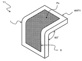
- FIG. 1 is a perspective view showing the overall structure of the RFID tag circuit element according to the present embodiment.
- this RFID circuit element T1 transmits and receives signals in a non-contact manner with an antenna of a RFID tag communication device (not shown), and is generally formed in a shape in which two planes are orthogonal to transmit and receive information.
- terms representing directions such as “left”, “right”, “up”, “down”, “horizontal plane”, “vertical plane”, “side surface”, etc. are used as appropriate.
- the configuration of this embodiment and the arrangement of each part are not limited to such postures and directions. That is, it can be used in a posture rotated or turned over from the posture shown in the figure (all other modified examples are the same).
- the tag antenna ANT1 has a dielectric substrate body (substrate body) 1 having a shape in which two flat plates are connected in an orthogonal arrangement.
- the dielectric substrate body 1 is composed of a horizontal substrate surface (fourth substrate surface) 1a disposed horizontally above in the illustrated posture and a vertical substrate surface (fifth substrate surface) 1b disposed vertically on the side.
- Each of the horizontal substrate surface 1a and the vertical substrate surface 1b has a substantially square plate shape made of a dielectric material such as ceramic, for example, and the entire dielectric substrate body 1 is disposed so that the substrate surfaces 1a and 1b are orthogonal to each other. It is formed as a single piece with one side connected.
- a side forming an angle of 90 ° (see FIG. 1) is referred to as an “inner angle side”, and the inner angle side and the opposite side across the substrate surfaces 1a and 1b (ie, 270)
- the side forming the angle of ° is referred to as the “outside angle side”.
- the end portion of the installation target is sandwiched, whereby the RFID circuit element T1 is installed on the installation target (see FIG. 4 described later).
- a microstrip antenna in which a conductor metal is formed into a thin film by vapor deposition or the like on the outer-angle-side surfaces of the horizontal substrate surface 1 a and the vertical substrate surface 1 b, that is, on the two surfaces opposite to the installation surface.
- a pattern 5 first conductor surface
- one continuous microstrip antenna pattern 5 is formed to extend over the horizontal substrate surface 1a and the vertical substrate surface 1b.
- a feeding point Ps described later is set at the center position of the microstrip antenna pattern 5 on the horizontal substrate surface 1a.
- the dielectric substrate body 1 and the microstrip antenna pattern 5 constitute a tag antenna ANT1.
- FIG. 2 is a cross-sectional view of the RFID circuit element T1 taken along the line II-II in FIG.
- the IC circuit unit 150 is embedded in the horizontal substrate surface 1a of the dielectric substrate body 1, and the IC circuit unit 150 includes the signal line 6, the matching circuit unit Ma, the signal line 6 ', and the power feed.
- the microstrip antenna pattern 5 is electrically connected through the point Ps.
- a surface terminal 7 of a thin metal plate is provided on the surface on the inner corner side of the horizontal substrate surface 1a (that is, the surface opposite to the microstrip antenna pattern 5 and the lower surface in the figure). Is electrically connected to the surface terminal 7 via a grounding wire 8 and a grounding point Pe.
- the matching circuit portion Ma matches the impedance at the feeding point Ps of the microstrip antenna pattern 5 with the impedance of the IC circuit portion, and normally uses elements such as a coil (L) and a capacitor (C), but the signal line This can also be realized by providing stubs and meander patterns at 6 and 6 '.
- an adhesive layer (fixing means) 9 made of an appropriate adhesive material is coated in a region other than the surface terminal 7 provided on the inner surface of the horizontal substrate surface 1a.
- this adhesive layer 9 is also coated on the entire inner surface of the other substrate surface (that is, the vertical substrate surface 1b in the present embodiment) of the dielectric substrate body 1 (hereinafter, each The same applies to the modified example).
- the RFID tag is stuck on the end part surface of an installation target object by sticking the adhesive bond layer 9 on the inner corner side surface of each board
- the circuit element T1 can be stably fixed.
- the entire surface of the adhesive layer 9 on each of the substrate surfaces 1a and 1b is covered with a release material layer (release paper or the like, not shown). And protect it. Further, except for FIG. 2, the adhesive layer 9 is omitted in order to avoid the complexity of the illustration.
- the surface of the installation part is made of a metal material.
- the RFID circuit element T1 of the present embodiment is installed on the surface of the metal plate M as an installation object, so that the metal plate M contacts the surface terminal 7, and the ground point Pe and the ground wire 8 It is electrically connected to the IC circuit unit 150 via This connection may be in a capacitive coupling state as long as it can be connected at a frequency used for communication and does not need to be connected in a DC manner. In this state, the metal plate M functions as a so-called ground plane.
- the substrate surfaces 1a and 1b of the dielectric substrate body 1 made of a dielectric material are connected to the microstrip antenna pattern 5 on the outer angle side surface and the inner angle. It becomes the structure pinched
- the metal plate M, the dielectric substrate body 1, and the entire microstrip antenna pattern 5 can function as a so-called microstrip antenna (patch antenna).
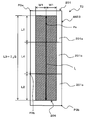
- FIG. 3 is a development view for explaining the dimension setting of the microstrip antenna pattern 5 in the present embodiment.
- FIG. 3 is a diagram in which the tag antenna ANT1 is developed in units of the substrate surfaces 1a and 1b with the microstrip antenna pattern 5 being continuous (in the corresponding FIGS. 7, 10, and 13 described later). The same).
- the microstrip antenna pattern (third pattern portion) 5 in the RFID circuit element T1 of the present embodiment has a long side that is roughly parallel to the extending direction across the horizontal substrate surface 1a and the vertical substrate surface 1b. It has a rectangular shape (substantially I shape).
- the feeding point Ps on the horizontal substrate surface 1a is provided in a direction perpendicular to the extending direction of the microstrip antenna pattern 5, that is, in the center position in the width direction (short side direction) of the microstrip antenna pattern 5 formed in a rectangular shape. (See dimension W1 in the figure). If it does in this way, among the high-frequency currents passing through the feed point Ps, the current component I W flowing in the width direction of the microstrip antenna pattern 5 will be canceled because it flows at the same magnitude in the opposite phase around the feed point Ps. It will be.
- a dielectric material is necessarily interposed between the microstrip antenna pattern 5 and the installation target object 10.
- the installation object 10 is a metal object, highly reliable information transmission / reception can be performed without causing a communication failure as in the case of using another type of tag antenna.
- the microstrip antenna pattern 5 is provided on the side opposite to the installation target 10 in the dielectric substrate body 1 as described above, the directivity range extends mainly on the side opposite to the installation target 10.
- the horizontal substrate surface 1a and the vertical substrate surface 1b are configured to be connected substantially orthogonally to each other (in other words, three-dimensionally connected), and a dielectric substrate body composed of the substrate surfaces 1a and 1b. 1 is provided so that the edge part of the installation target object 10 may be inserted
- the dielectric substrate body 1 becomes a three-dimensional structure provided in the vicinity of the end portion of the installation target object 10 and has a characteristic in which the directivity range is widened on the opposite side of the installation target object 10 when viewed from the respective substrate surfaces 1a and 1b. It becomes.
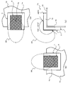
- FIGS. 4A to 4C are three views showing the directivity range 20 of the above-described RFID tag circuit element T1.
- 4A is a plan view seen from the arrow IVa in FIG. 1
- FIG. 4B is a front view seen from the arrow IVb in FIG. 1
- FIG. It is the side view seen from arrow IVc inside.
- two orthogonal metal plates are integrally connected to form the installation object 10, and the RFID circuit element T1 is installed at the end.
- the planes of the microstrip antenna patterns 5 on the horizontal substrate surface 1a and the vertical substrate surface 1b are set.
- the directivity range 20 (communicable region) as a whole is formed by combining the directivity ranges generated in the orthogonal directions. That is, as shown in FIG. 4C, one large directivity range 20 is formed so as to evenly cover the microstrip antenna patterns 5 on the horizontal substrate surface 1a and the vertical substrate surface 1b arranged orthogonally. .
- the directivity range 20 is formed in a wide angle range including a direction orthogonal to the plane of the horizontal substrate surface 1a, a direction orthogonal to the plane of the vertical substrate surface 1b, and a direction therebetween. It can be formed in an angle range of about 180 ° to 210 ° (depending on the material and dimension setting of each member).
- the tag antenna ANT1 as a whole including the two substrate surfaces 1a and 1b is synthesized with the above-described characteristics (characteristics in which the directivity range is widened on the opposite side of the installation object 10 when viewed on each of the substrate surfaces 1a and 1b).
- a wide directivity range 20 having a complex three-dimensional shape that extends three-dimensionally from the end of the installation object 10 toward the side opposite to the installation object 10 can be realized.
- the vertical substrate surface 1b can be disposed as a side surface (vertical surface).
- the microstrip antenna is directed outward from the vicinity of the end of the installation target 10 corresponding to a combination of the directivity range extending upward from the upper surface and the directivity range extending laterally from the side surface.
- a wide directivity range 20 having such a composite three-dimensional shape can be realized.
- the installation object 10 is a metal object, a wide directivity range can be reliably realized and good information transmission / reception can be performed.
- the feeding point Ps is provided at a substantially central position in the width direction (direction perpendicular to the extending direction) in the microstrip antenna pattern 5 formed in a rectangular shape.
- the resonance frequency and antenna sensitivity of the antenna can be set by the extending direction dimension L1.
- the antenna sensitivity in the direction along the horizontal substrate surface 1a and the antenna sensitivity in the direction along the vertical substrate surface 1b can be made substantially equal to each other.
- the antenna sensitivity in each direction can be equalized for the entire tag antenna ANT1.
- the IC circuit unit 150 and the matching circuit unit Ma are connected to the feeding point Ps and arranged so as to be embedded in the middle part in the thickness direction of the dielectric substrate body 1, thereby providing the IC circuit unit.
- the RFID circuit element T1 can be integrated into the tag antenna ANT1 without projecting 150 to the outside of the tag antenna ANT1.
- the adhesive layer 9 for fixing to the installation target object 10 is provided on the surface of the dielectric substrate body 1 on the side where the end of the installation target object 10 is sandwiched.
- the entire RFID circuit element T1 can be reliably fixed to the object 10.
- the adhesive layer 9 as a fixing means for the RFID circuit element T 1 for example, the substrate surface 1 a, 1 b on either or both of the dielectric substrate body 1 and the installation object 10 are penetrated. Fasteners such as screws and bolts to be fastened may be used (not shown).
- the ground plane is placed on the surface (inner corner side surface) of the dielectric substrate body 1 that sandwiches the end of the installation object 10.
- angular part was formed in the edge part which the two board
- the tag antenna ANT1 provided with the microstrip antenna pattern 5 having a rectangular shape (substantially I shape) in the unfolded state is used.
- deployment state it is not restricted to this, For example, you may use the microstrip antenna pattern formed in the substantially L shape in the expansion
- FIG. 6 (a) and 6 (b) are perspective views showing the overall structure of the RFID circuit element T2 according to such a modification.
- FIG. 6A is a perspective view seen from the top side of the tag antenna
- FIG. 6B is a perspective view seen from the concave side of the tag antenna.
- FIG. 6A is a perspective view seen from the top side of the tag antenna
- FIG. 6B is a perspective view seen from the concave side of the tag antenna.
- the RFID tag circuit element T2 of this modification example is formed with a tag antenna (microstrip antenna) ANT2 that is formed in a shape that is substantially orthogonal to three planes and transmits / receives information. And an IC circuit unit 150 (see FIG. 2) embedded in the tag antenna ANT2.
- the tag antenna ANT2 has a dielectric substrate body (substrate body) 101 having a shape in which three flat plates are connected in an orthogonal arrangement.
- the dielectric substrate body 101 has a horizontal substrate surface (intermediate substrate surface) 101a horizontally disposed upward and a left substrate surface (first substrate surface) 101b disposed vertically on the left side. And a right side substrate surface (second substrate surface) 101c arranged vertically on the right side.
- Each of the horizontal substrate surface 101a, the left side substrate surface 101b, and the right side substrate surface 101c has a substantially square flat plate shape made of a dielectric material such as ceramic, for example.
- 101a, 101b, and 101c are formed as an integrated body in which one side is connected in an orthogonal arrangement.
- the side that forms an angle of 90 ° (see FIG. 6B) of the two orthogonal substrate surfaces 101a and 101b is referred to as the “inner angle side” and the opposite side as the “outer angle side”.
- the inner substrate surfaces of the horizontal substrate surface 101a, the left substrate surface 101b, and the right substrate surface 101c of the dielectric substrate body 101, that is, adjacent substrate surfaces form an angle of 90 ° with each other.
- the top surface covers the apex of the object to be installed of the RFID circuit element T2, and thereby the RFID circuit element T2 is installed on the object to be installed (described later). 8).
- the microstrip antenna pattern 105 similar to the microstrip antenna pattern 5 is formed on the surfaces of the substrate surfaces 101a, 101b, and 101c on the outer corner side, that is, on the three surfaces opposite to the installation surface. (First conductor surface) is provided, and is formed so as to extend from the left side substrate surface 101b through the horizontal substrate surface 101a to the right side substrate surface 101c.
- a feeding point Ps is set at the center position of the microstrip antenna pattern 105 on the horizontal substrate surface 101a.
- the dielectric substrate body 101 and the microstrip antenna pattern 105 constitute a tag antenna ANT2.
- Other configurations are the same as those of the above-described embodiment, and a description thereof will be omitted.
- FIG. 7 is a development view for explaining the dimension setting of the microstrip antenna pattern 105 in the present modification, and corresponds to FIG. 3 of the above embodiment.
- the microstrip antenna pattern 105 in the RFID tag circuit element T2 of the present modification is roughly a rectangular shape having long sides parallel to the extending direction across the horizontal substrate surface 101a and the left side substrate surface 101b.
- the formed first pattern portion 102a and the second pattern portion 102b formed in a rectangular shape having a long side parallel to the extending direction across the horizontal substrate surface 101a and the right side substrate surface 101c are formed. It is formed in a substantially L shape that is overlapped so as to share a part.
- the feeding point Ps on the horizontal substrate surface 101a is provided in a direction orthogonal to the extending direction of the pattern portions 102a and 102b, that is, at the center position in the width direction (short side direction) of the pattern portions 102a and 102b ( (See dimension W1 in the figure).
- the long sides of the pattern portions 102a and 102b are equal to each other, and are formed to have a length L1 that is approximately a half of the wavelength ⁇ 1 of the communication radio wave considering the dielectric constant of the dielectric substrate 101. .
- the lengths L1 of the long sides of the pattern portions 102a and 102b are equal.
- each of the substrate surfaces 101a, 101b, and 101c with a dielectric, a dielectric always exists between the microstrip antenna pattern 105 and the installation target 110, so that the installation target 110 is a metal object. Even in such a case, highly reliable information transmission / reception can be performed without causing a communication failure as in the case of using another type of tag antenna.
- the directivity range mainly extends on the opposite side of the installation target object 110.
- the substrate surfaces 101a, 101b, and 101c are configured such that adjacent substrate surfaces are connected to each other substantially orthogonally (in other words, three-dimensionally connected), and the substrate surfaces 101a, 101b, 101c,
- the dielectric substrate body 101 made of 101c is provided so as to cover an end (or apex) of the installation object 110.
- the dielectric substrate 101 becomes a three-dimensional structure provided in the vicinity of the apex of the installation target 110, and the directivity range is widened on the opposite side of the installation target 110 when viewed from each of the substrate surfaces 101a, 101b, and 101c. It becomes a characteristic.
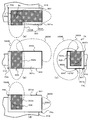
- FIGS. 8A to 8C are three views showing the directivity of the RFID tag circuit element T2 of the present modification, and correspond to FIGS. 4A to 4C of the above embodiment.
- 8A is a plan view seen from the arrow VIIIa in FIG. 6A
- FIG. 8B is a front view seen from the arrow VIIIb in FIG. 6A
- (C) is the side view seen from arrow VIIIc in Fig.6 (a).
- three orthogonal metal plates are integrally connected to constitute the installation object 110, and the RFID tag circuit element T2 is installed so as to cover the apex.
- the directivity range 120A is formed in a wide angle range including a direction orthogonal to the plane of the horizontal substrate surface 101a, a direction orthogonal to the plane of the left side substrate surface 101b, and a direction therebetween. It can be formed in an angle range of about 180 ° to 210 ° (depending on the material and dimension setting of each member). Also in the second pattern portion 102b, a directivity range 120B having a wide angular range is formed so as to cover the microstrip antenna patterns 105 on the horizontal substrate surface 101a and the right side substrate surface 101c.
- the dielectric substrate body 101 as a whole composed of these three substrate surfaces 101a, 101b, and 101c is in the vicinity of the top of the installation object 110 corresponding to the synthesized characteristics of the two directivity ranges 120A and 120B.
- a wide directivity range 120 having a three-dimensional composite shape that spreads three-dimensionally toward the outside of the corner opposite to the installation object 110 can be realized.
- the microstrip antenna pattern 105 has the same length dimension L1 of the entire long sides of the first pattern portion 102a and the second pattern portion 102b that share a part with each other on the horizontal substrate surface 101a. It has become. Thereby, the resonant frequency of the antenna by the 1st pattern part 102a and the resonant frequency of the antenna by the 2nd pattern part 102b can be made to correspond. And the sensitivity of the whole tag antenna ANT2 can be improved by matching the frequencies of the two pattern portions 102a and 102b in this way (squeezing to a narrow range without greatly different frequencies).
- the extending direction dimension L2 of the portion existing on the horizontal substrate surface 101a is equal to the extending direction dimension L2 of the portion existing on the left side substrate surface 101b.
- the extending direction dimension L2 of the portion existing on the horizontal substrate surface 101a is equal to the extending direction dimension L2 of the portion existing on the right side substrate surface 101c.
- the antenna sensitivity in the direction along the horizontal substrate surface 101a and the antenna sensitivity in the direction along the right side substrate surface 101c can be made substantially equal.
- the antenna sensitivity in each direction can be equalized for the entire tag antenna ANT2.
- the feeding point Ps is a substantially central position in the direction orthogonal to the extending direction of the first pattern portion 102a and extends of the second pattern portion 102b. It is provided at a position that is substantially the center position in a direction orthogonal to the direction.
- the resonance frequency and antenna sensitivity of the antenna can be set mainly by the extending direction dimension L1 of the pattern portions 102a and 102b.
- the microstrip antenna pattern 105 has a gap between the first pattern portion 102a and the second pattern portion 102b in a portion where the left side substrate surface 101b and the right side substrate surface 101c are close to each other. It is provided on the left side substrate surface 101b and the right side substrate surface 101c so that 111 is interposed. Thereby, the first pattern portion 102a extending in the extending direction on the left side substrate surface 101b and the second pattern portion 102b extending in the extending direction on the right side substrate surface 101c can be prevented from being electrically connected to each other. As a result, the resonance frequency and antenna sensitivity of the antenna can be surely set mainly by the extending direction dimension L1 of the pattern portions 102a and 102b.
- the microstrip antenna pattern formed in a substantially I shape is used on three surfaces
- the microstrip antenna pattern has a substantially I shape in a developed state
- the formed microstrip antenna pattern may be provided on three substrate surfaces.
- FIG. 9 is a perspective view showing the entire structure of the RFID circuit element T3 according to such a modification.
- FIG. 9A is a perspective view looking down at the tag antenna
- FIG. 9B is a perspective view looking up at the tag antenna from the back side (the back side in FIG. 9A). is there.
- three vertices P3a, P3b, and P3c with reference numerals are shown for reference for confirming the arrangement relationship of each member. Parts equivalent to those of the above embodiment and the modified example of (1) are denoted by the same reference numerals, and description thereof is omitted or simplified as appropriate.
- the dielectric substrate body (substrate body) 201 of the tag antenna ANT3 has three substrate surfaces, and one substrate The other two substrate surfaces are orthogonally connected to two sides located on the opposite sides of the surface. That is, the dielectric substrate body 201 includes an upper substrate surface (first substrate surface) 201a that is horizontally disposed upward in the posture of FIG. 9A and a middle substrate surface (intermediate substrate surface) 201b that is vertically disposed laterally. And a lower substrate surface (second substrate surface) 201c horizontally disposed below.
- Each of the upper substrate surface 201a, the middle substrate surface 201b, and the lower substrate surface 201c has a substantially square plate shape made of a dielectric material such as ceramic, for example, and the entire dielectric substrate body 201 is formed of the substrate surface 201a, Two adjacent substrate surfaces of 201b and 201c are formed as an integrated body in which one side is connected in an arrangement that is orthogonal to each other.
- the side that forms an angle of 90 ° is the opposite side to the “inner angle side”. This is referred to as the “outside corner side”.
- the inner substrate surfaces of the upper substrate surface 201a, middle substrate surface 201b, and lower substrate surface 201c of the dielectric substrate body 201 that is, three surfaces that form an angle of 90 ° with each other adjacent substrate surfaces
- the microstrip antenna pattern 205 (first conductor surface) is provided on each of the outer surfaces of the substrate surfaces 201a, 201b, and 201c, that is, on the three surfaces opposite to the installation surface. It is formed so as to extend from the upper substrate surface 201a through the middle substrate surface 201b to the lower substrate surface 201c.
- the dielectric substrate body 201 and the microstrip antenna pattern 205 constitute a tag antenna ANT3.
- a feeding point Ps is set at the center position of the microstrip antenna pattern 205 on the upper substrate surface 201a.
- Other configurations are the same as those of the above-described embodiment, and a description thereof will be omitted.
- FIG. 10 is a development view for explaining the dimension setting of the microstrip antenna pattern 205 in this modification, and corresponds to FIG. 3 and FIG.
- the microstrip antenna pattern 205 in the RFID circuit element T3 of the present modification is roughly a length parallel to the extending direction from the upper substrate surface 201a through the middle substrate surface 201b to the lower substrate surface 201c. It is formed in a rectangular shape (substantially I shape) having sides.
- the feeding point Ps on the upper substrate surface 201a is provided at a central position in the direction perpendicular to the extending direction of the microstrip antenna pattern 205, that is, in the width direction (short side direction) of the microstrip antenna pattern 205 formed in a rectangular shape. (See dimension W1 in the figure).
- the length L3 of the long side of the microstrip antenna pattern 205 determines the wavelength of the communication radio wave.
- it is formed on the long side length L3 is the length of approximately half the first communication radio wave of a wavelength lambda 2 when considering the dielectric constant of the dielectric substrate 201 of the microstrip antenna pattern 205.
- the length in the long side direction of the portion existing on the upper substrate surface 201a and the portion existing on the lower substrate surface 201c are equal to the same length L2.
- FIGS. 11A to 11D are four views showing the directivity of the RFID circuit element T3 according to this modification.
- FIGS. 4A to 4C and FIGS. It is a figure corresponding to. 11A is a plan view seen from the arrow XIa in FIG. 9A, and FIG. 11B is a front view seen from the arrow XIb in FIG. 9A.
- (C) is the side view seen from arrow XIc in Fig.9 (a)
- FIG.11 (d) is the bottom view seen from arrow XId in FIG.9 (b).
- a so-called grooved steel in which three metal plates are integrally connected to form a substantially U-shaped cross section constitutes an installation object 210, and this end portion is connected to the RFID circuit element T3. Is shown in a state where it is installed so as to be sandwiched.
- the two upper substrates when transmitting / receiving a radio wave signal with the tag antenna ANT3, the two upper substrates arranged so as to face each other while covering the entire middle substrate surface 201b located in the middle.
- One large directivity range 220 is formed so as to evenly cover the microstrip antenna patterns 205 on the surface 201a and the lower substrate surface 201c.
- the directivity range 220 is formed in a wide angle range including a direction orthogonal to the plane of the upper substrate surface 201a, a direction orthogonal to the plane of the lower substrate surface 201c, and a direction between them. (Depending on the material and dimensions of the material), it can be formed in an angle range of approximately 240 ° to 300 °.
- a directivity range extending upward from the upper substrate surface 201, a directivity range extending laterally from the middle substrate surface 201b, and a directivity range extending downward from the lower substrate surface 201c are supported.
- a wide directivity range 220 having a composite solid shape that extends outward from the vicinity of the end of the installation object 210 can be realized. Therefore, in this modification as well, as in the modification of the above embodiment and (1), even if the installation object 210 is a metal object, a wide directivity range 220 is surely realized and good information transmission / reception is performed. Can do.
- the feeding point Ps is provided at a substantially central position in the direction perpendicular to the extending direction of the microstrip antenna pattern 205.
- the currents flowing on one side and the other side in the direction orthogonal to the extending direction in other words, the width direction
- the resonance frequency and antenna sensitivity of the antenna can be set mainly by the extending direction dimension of the substantially I-shaped microstrip pattern.
- the microstrip antenna pattern formed in a substantially L shape is used on four surfaces
- the microstrip antenna pattern 105 formed in a substantially L shape in the developed state is formed on three substrate surfaces.
- the present invention is not limited to this.
- microstrip antenna patterns formed in an approximately L shape may be provided on four substrate surfaces.
- FIG. 12 is a perspective view showing the entire structure of the RFID circuit element T4 according to such a modification.
- 12A is a perspective view looking down at the tag antenna
- FIG. 12B is a perspective view looking up at the tag antenna from the back side (the back side in FIG. 12A). is there.
- three vertices P4a, P4b, and P4c with reference numerals are shown for reference for confirming the arrangement relationship of each member. Parts equivalent to those in the above embodiment and the modified examples of (1) and (2) are denoted by the same reference numerals, and description thereof will be omitted or simplified as appropriate.
- the dielectric substrate body (substrate body) 301 of the tag antenna ANT4 has four substrate surfaces. That is, with respect to the three U-shaped substrate surfaces in the modification (2), another substrate surface is connected to the other three substrate surfaces on the side surface.
- the dielectric substrate body 301 includes a top substrate surface (intermediate substrate surface) 301a that is horizontally disposed upward in the posture of FIG. 12A, and a front substrate surface (first substrate surface) 301b that is vertically disposed on the right front side.
- a side substrate surface (second substrate surface) 301c vertically arranged on the left side and a bottom substrate surface (third substrate surface) 301d horizontally arranged below.
- Each of the top substrate surface 301 a, the front substrate surface 301 b, the side substrate surface 301 c, and the bottom substrate surface 301 d has a substantially square plate shape made of a dielectric material such as ceramic, for example.
- the whole is formed as an integrated body in which two adjacent substrate surfaces of the substrate surfaces 301a, 301b, 301c, and 301d are connected to each other in an orthogonal arrangement.
- the three substrate surfaces 301a, 301c, and 301d forming the U-shape are in a direction orthogonal to the extending direction because of the dimension setting of the microstrip antenna pattern 305 described later.
- the dimension is about twice as long as that of the first modification.
- the side forming the 90 ° angle (see FIG. 12B) of the two orthogonal substrate surfaces 301a and 301b is referred to as “inner angle side”.
- the opposite side is referred to as the “outside corner side”.
- the top substrate surface 301a, the front substrate surface 301b, the side substrate surface 301c, and the bottom substrate surface 301d of the dielectric substrate body 301 are each 90 ° at the inner surfaces, that is, adjacent substrate surfaces.
- 4 surfaces cover the two apexes of the installation target of the RFID circuit element T4, and thereby the RFID circuit element T4 is installed on the installation object (see FIG. 14 described later).
- the microstrip antenna pattern 305 (first conductor surface) is provided on the outer surface of each of the substrate surfaces 301a, 301b, 301c, and 301d, that is, on the four surfaces opposite to the installation surface.
- the bottom substrate surface 301d extends from the side substrate surface 301c and the top substrate surface 301a to the front substrate surface 301b.
- the dielectric substrate 301 and the microstrip antenna pattern 305 constitute a tag antenna ANT4.
- the microstrip antenna pattern 305 passing through the bottom substrate surface 301d and the side substrate surface 301c and the microstrip antenna pattern 305 on the front substrate surface 301b are arranged apart from each other with a gap 311 therebetween. Is not connected.
- a feeding point Ps is set at the center position of the microstrip antenna pattern 305 on the top substrate surface 301a.
- Other configurations are the same as those of the above-described embodiment, and a description thereof is omitted.
- FIG. 13 is a development view for explaining the dimension setting of the microstrip antenna pattern 305 in this modification, and corresponds to FIG. 3, FIG. 7, and FIG.
- the microstrip antenna pattern 305 in the RFID tag circuit element T4 of the present modification is roughly a rectangular shape having long sides parallel to the extending direction across the top substrate surface 301a and the front substrate surface 301b.
- the formed first pattern portion 302a and the second pattern portion 302b formed in a rectangular shape having a long side parallel to the extending direction from the top substrate surface 301a through the side substrate surface 301c to the bottom substrate surface 301d.
- the top substrate surface 301a is formed in a substantially L shape so as to be partially shared.
- the feeding point Ps on the top substrate surface 301a is provided in a direction perpendicular to the extending direction of the pattern portions 302a and 302b, that is, in the center position in the width direction (short side direction) of the pattern portions 302a and 302b ( (See dimension W1 in the figure).
- the long sides of the pattern portions 302a and 302b are formed to have a length L3 that is a half of the wavelength ⁇ 2 of the communication radio wave when the same dielectric substrate 301 is considered.
- the length in the long side direction of each of the portion present on the top substrate surface 301a and the portion present on the bottom substrate surface 301d is equal to the same length L2.
- the length in the long side direction of the portion existing on the front substrate surface 301b is equal to the length L2 and exists on the top substrate surface 301a.
- FIGS. 14A to 14D are four views showing the directivity of the RFID tag circuit element T4 of this modification.
- FIGS. 4A to 4C and FIGS. 12 is a diagram corresponding to FIG. 11 (a) to (d).
- 14A is a plan view seen from the arrow XIVa in FIG. 12A
- FIG. 14B is a front view seen from the arrow XIVb in FIG. (C) is the side view seen from arrow XIVc in FIG. 12 (a)
- FIG.14 (d) is the bottom view seen from arrow XIVd in FIG.12 (b).
- a metal body formed in a rectangular parallelepiped shape constitutes the installation object 310, and the RFID tag circuit element T4 is installed so as to sandwich a corner including two adjacent vertices. Is shown.
- the directivity ranges 320A and 320B generated by the pattern portions 302a and 302b are combined so as to be combined.
- the directivity range is formed. That is, in the second pattern portion 302b, the entire side substrate surface 301c positioned in the middle is covered, and the microstrip antenna patterns 305 of the two top substrate surfaces 301a and the bottom substrate surface 301d arranged opposite to each other are equally provided.
- One large directivity range 320B is formed.
- the directivity range 320B is formed in a wide angle range including a direction orthogonal to the plane of the top substrate surface 301a, a direction orthogonal to the plane of the bottom substrate surface 301d, and a direction therebetween. (Depending on the material and size of the material), it can be formed in an angle range of approximately 240 ° to 270 °. Also in the first pattern portion 302a, one large directivity range 320A is formed so as to cover the microstrip antenna patterns 305 on the top substrate surface 301a and the front substrate surface 301b arranged orthogonally.
- the length L5 in the extending direction of the microstrip antenna pattern 305 existing on the top substrate surface 301a is longer than the length L2 in the extending direction of the microstrip antenna pattern 305 existing on the front substrate surface 301b.
- the directivity range 320A is formed so as to be largely biased toward the top substrate surface 301a.
- the dielectric substrate body 301 as a whole comprising the four substrate surfaces 301a, 301b, 301c, 301d corresponds to a combination of the characteristics of the two directivity ranges 320A, 320B.
- An even wider compound directivity range 320 can be realized. Therefore, in this modification, even if the installation object 310 is a metal object, a wide directivity range 320 can be reliably realized and good information transmission / reception can be performed.
- the case where the RFID tag circuit elements T1 and T4 are installed is exemplified by a metal plate, a thin steel, or a metal body.
- OA equipment, a steel desk, a steel shelf, a back cover of a binder, etc. can also be installed on other metal objects, and in this case, the same effect is obtained.
- FIG. 2 is a cross-sectional view of the RFID circuit element according to the II-II cross section in FIG. 1. It is an expanded view for demonstrating the dimension setting of a microstrip antenna pattern. It is a 3rd page figure which shows the directivity of a radio
- Dielectric substrate (substrate body) 1a Horizontal substrate surface (4th substrate surface) 1b Vertical substrate surface (5th substrate surface) 5 Microstrip antenna pattern (first conductor surface) 9 Adhesive layer (fixing means) 10 Installation Object 20 Directional Range 101 Dielectric Substrate (Substrate Body) 101a Horizontal substrate surface (intermediate substrate surface) 101b Left side substrate surface (first substrate surface) 101c Right side substrate surface (second substrate surface) 102a 1st pattern part 102b 2nd pattern part 105 Microstrip antenna pattern (1st conductor surface) DESCRIPTION OF SYMBOLS 110 Installation object 111 Cavity part 120 Directional range 120A, B Directional range 150 IC circuit part 201 Dielectric board body (board body) 201a Upper substrate surface (first substrate surface) 201b Middle substrate surface (intermediate substrate surface) 201c Lower substrate surface (second substrate surface) 205 Microstrip antenna pattern (first conductor surface) 210 Installation Object 220 Directional Range 301 Dielectric Substrate Body (Subs
Landscapes
- Waveguide Aerials (AREA)
- Details Of Aerials (AREA)
- Variable-Direction Aerials And Aerial Arrays (AREA)
Abstract
【課題】設置対象物が金属物であっても確実に広い指向性範囲を実現し、良好な情報送受信を行う。
【解決手段】情報を記憶するIC回路部150と、情報を送受信するタグアンテナANT2とを有し、設置対象物110に取り付けられる無線タグ回路素子T2であって、タグアンテナANT2は、隣り合う面同士が互いに略直交して連接するように設けられた3つ以上の誘電体の基板面101a,101b,101cからなり、設置対象物110の頂点を覆うように設けられた誘電基板体101と、この誘電基板体101のうち、設置対象物110を覆う側と反対側に形成され、IC回路部150に接続される給電点Psを備えたマイクロストリップアンテナパターン105とを有するマイクロストリップアンテナである。
Description
本発明は、外部と情報の無線通信が可能である無線タグ回路素子に関するものである。
小型の無線タグとリーダ(読み取り装置)/ライタ(書き込み装置)との間で非接触で情報の読み取り/書き込みを行うRFID(Radio Frequency Identification)システムが知られている。無線タグは、情報を記憶するIC回路部と情報の送受信を行うタグアンテナとからなる無線タグ回路素子を備えている。そして、無線タグが汚れている場合や見えない位置に配置されている場合であっても、リーダ/ライタ側よりIC回路部の情報に対してアクセス(情報の読み取り/書き込み)が可能であり、既に種々の分野において実用化されている。
上記のような無線タグ回路素子において、例えば、タグアンテナに、平面アンテナの一種であるマイクロストリップアンテナを用いたものが、既に提唱されている(例えば、特許文献1参照)。
この従来技術では、誘電体上に、線路の特性インピーダンスの大きいマイクロストリップアンテナパターン(マイクロストリップライン)と、線路の特性インピーダンスの小さいマイクロストリップアンテナパターン(マイクロストリップライン不連続部)とを交互に配列することで、LとCで構成されるローパスフィルターを形成している。給電点から励振された電磁波は、上記構成のマイクロストリップ線路を介して、最終のマイクロストリップアンテナパターンの先端に到達し、アンテナとしての特性を示すようになっている。
特開2000-278027号公報
近年、無線タグの利用の拡大によってその用途は多種多様となっており、それらの用途に応じた多様な態様の無線タグが望まれている。例えばOA機器や、スチールデスク、スチール棚、バインダーの背表紙等、金属物に対し無線タグを設けたいというニーズが生じつつある。上記従来技術では、基板面を誘電体で構成することにより、マイクロストリップアンテナパターンと設置対象物との間に必ず誘電体が介在する。この結果、設置対象物が金属物であった場合でも、他のタイプのタグアンテナを用いる場合のように通信障害を招くことはない。しかしながら、アンテナ全体が略平板状の(平面的な)構造であるため、金属物に設置した場合には、マイクロストリップアンテナパターンからの指向性範囲が、主として設置対象物と反対側の比較的狭い範囲に限定されるという問題があった。
本発明の目的は、設置対象物が金属物であっても確実に広い指向性範囲を実現し、良好な情報送受信を行うことのできる無線タグ回路素子を提供することにある。
上記目的を達成するために、第1の発明は、情報を記憶するIC回路部と、情報を送受信するタグアンテナとを有し、設置対象物に取り付けられる無線タグ回路素子であって、前記タグアンテナは、隣り合う面同士が互いに略直交して連接するように設けられた3つ以上の誘電体の基板面からなり、前記設置対象物の端部又は頂点において当該設置対象物の複数面を同時に覆うように又は挟み込むように設けられた基板体と、前記基板体のうち、前記設置対象物を覆う側又は挟み込む側と反対側に形成され、前記IC回路部に接続される給電点を備えた第1導体面と、前記基板体のうち、前記設置対象物を覆う側又は挟み込む側に設けられた接地点とを有するマイクロストリップアンテナであることを特徴とする。
本願第1発明の無線タグ回路素子は、タグアンテナとして、マイクロストリップアンテナと基板体とを備えたマイクロストリップアンテナを用いる。基板体は3つ以上の基板面で構成し、第1導体面(いわゆるマイクロストリップアンテナパターン)はその基板体のうち(無線タグ回路素子の)設置対象物とは反対側に設けている。基板面を誘電体で構成することにより、第1導体面は、設置対象物との間に必ず誘電体が介在することとなる。この結果、設置対象物が金属物であった場合でも、他のタイプのタグアンテナを用いる場合のように通信障害を招くことなく、信頼性の高い情報送受信を行うことができる。
一方、一般にマイクロストリップアンテナでは、基板の面方向に交差するように指向性範囲が広がる。本願第1発明では、第1導体面を上記のように基板体のうち設置対象物とは反対側に設けていることから、主として設置対象物と反対側に指向性範囲が広がる。このとき、3つ以上の基板面は、隣り合う基板面同士が互いに略直交して連接するように(言い換えれば立体的に接続するように)構成されており、それら基板面からなる基板体は、設置対象物の端部(又は頂点)を覆うように(又は挟み込むように)設けられている。したがって、基板体は、設置対象物の端部や頂点近傍に設けられる立体的な構造物となり、各基板面ごとで見ると設置対象物と反対側に指向性範囲が広がる特性となる。この結果、それら3つ以上の基板からなる基板体全体としては、上記の各特性を合成したものに対応した、上記設置対象物の端部や頂点近傍から設置対象物と反対側に向かって3次元的に広がる、複合立体形状の広い指向性範囲を実現することができる。
以上のようにして、本願第1発明においては、設置対象物が金属物であっても確実に広い指向性範囲を実現し、良好な情報送受信を行うことができる。
第2発明は、上記第1発明において、前記基板体に備えられた前記3つ以上の基板面は、略四角形形状の中間基板面と、前記中間基板面の前記略四角形形状の4辺のうち1辺において連接し、面方向が前記中間基板面と略直交する第1基板面と、前記中間基板面の前記略四角形形状の4辺のうち他の1辺において連接し、面方向が前記中間基板面と略直交する第2基板面とを備えており、前記第1導体面は、少なくとも前記第1基板面から前記中間基板面を通り前記第2基板面にわたるようにしつつ、前記3つ以上の前記基板面にわたり設けられていることを特徴とする。
これにより、互いに直交しつつ連接する第1基板面、中間基板面、第2基板面に沿った、複合立体形状の広い指向性範囲を確実に実現することができる。
第3発明は、上記第2発明において、前記基板体は、前記第1基板面、前記中間基板面、及び前記第2基板面が、展開した状態において略I字状となるように構成されており、前記給電点を、前記第1基板面、中間基板面又は前記第2基板面の前記第1導体面に設けたことを特徴とする。
展開状態において略I字状であることにより、(展開しない)通常の3次元的形状においては、第1基板面、中間基板面、第2基板面で、略コの字となるような形状とすることが可能である。これにより、これら3つの基板面で設置対象物の端部を挟み込む(又は覆う)ようにして配置することができる。
この場合、第1基板面を上面(水平面)として配置すると、中間基板面を鉛直方向の側面として配置でき、第2基板面を下面(水平面)として配置することができる。すなわちこの場合、マイクロストリップアンテナとして、上面から上方に広がる指向性範囲と、側面から側方に広がる指向性範囲と、下面から下方に広がる指向性範囲とを合成したものに対応した、上記設置対象物の端部近傍から外方へ向かうような複合立体形状の広い指向性範囲を実現することができる。
第4発明は、上記第2発明において、前記基板体は、前記第1基板面、前記中間基板面、及び前記第2基板面が、展開した状態において略L字状となるように構成されており、前記給電点を、前記中間基板面の前記第1導体面に設けたことを特徴とする。
展開状態において略L字状であることにより、(展開しない)通常の3次元的形状においては、第1基板面のうち中間基板面へ連接する部分に隣接する部分と、第2基板面のうち中間基板面へ連接する部分に隣接する部分とが、互いに付き合わせられるような形状(例えば中間基板面、第1基板面、第2基板面が、直方体の1頂点を含む3つの面を構成するような形状)とすることが可能である。そして、上記1頂点が設置対象物のコーナー(頂点)に該当するように、基板体を当該設置対象物の頂点を覆う(又は挟み込む)ようにして配置することができる。
この場合、中間基板面を上面(水平面)として配置すると、第1基板面及び第2基板面は互いに直交する2側面(鉛直面)として配置される。すなわちこの場合、マイクロストリップアンテナとして、上面から上方に広がる指向性範囲と、2つの側面から側方にそれぞれ広がる指向性範囲とを合成したものに対応した、上記設置対象物のコーナー近傍から外方へ向かうような複合立体形状の広い指向性範囲を実現することができる。
第5発明は、上記第4発明において、前記第1導体面は、前記中間基板面において互いに一部を共有しつつ、前記中間基板面から少なくとも前記第1基板面にわたって延設された第1パターン部、及び、前記中間基板面から少なくとも前記第2基板面にわたって延設された第2パターン部、を備えており、前記第1パターン部の前記延設方向寸法と、前記第2パターン部の前記延設方向寸法とが略等しくなっていることを特徴とする。
これにより、第1パターン部によるアンテナの共振周波数と、第2パターン部によるアンテナの共振周波数とを略一致させることができる。そしてこのように2つのパターン部による周波数を略一致させる(周波数を大きく異ならせずに狭い範囲に絞る)ことにより、アンテナ全体の感度を向上することができる。
第6発明は、上記第5発明において、前記第1パターン部は、前記中間基板面に存在する部分の前記延設方向寸法と、前記第1基板面に存在する部分の前記延設方向寸法とが略等しくなっており、前記第2パターン部は、前記中間基板面に存在する部分の前記延設方向寸法と、前記第2基板面に存在する部分の前記延設方向寸法とが略等しくなっていることを特徴とする。
これにより、第1パターン部において中間基板面に沿った方向におけるアンテナ感度と第1基板面に沿った方向におけるアンテナ感度とを略等しくすることができる。同様に、第2パターン部において中間基板面に沿った方向におけるアンテナ感度と第2基板面に沿った方向におけるアンテナ感度とを略等しくすることができる。以上の結果、アンテナ全体として、各方向に対するアンテナ感度を均等化することができる。
第7発明は、上記第5又は第6発明において、前記給電点は、前記第1パターン部のうち前記延設方向と直交する方向における略中央位置であると共に、前記第2パターン部のうち前記延設方向と直交する方向における略中央位置となる位置に、設けられていることを特徴とする。
これにより、第1及び第2パターン部において、給電点を基準に、延設方向と直交する方向(言い換えれば幅方向)における一方側及び他方側でそれぞれ流れる電流を互いに略相殺することができる。この結果、主として各パターン部の延設方向寸法によってアンテナの共振周波数やアンテナ感度を設定することができる。
第8発明は、上記第7発明において、前記第1導体面は、前記第1基板面と前記第2基板面とが近接する部分において、前記第1パターン部と前記第2パターン部との間に空隙部が介在するように、前記第1基板面及び前記第2基板面に設けられていることを特徴とする。
これにより、第1基板面において延設方向に延びる第1パターン部と第2基板面において延設方向に延びる第2パターンとが、互いに導通するのを防止することができる。この結果、主として、各パターン部の延設方向寸法によってアンテナの共振周波数やアンテナ感度を確実に設定することができる。
第9発明は、上記第8発明において、前記基板体は、前記中間基板面、前記第1基板面、前記第2基板面に加え、前記第2基板面の前記中間基板面と反対側の部分に連接し、面方向が前記第2基板面と略直交する第3基板面を備えており、前記第1導体面の前記第2パターン部は、前記中間基板面から前記第2基板面を通り前記第3基板面にわたるように設けられていることを特徴とする。
本願第9発明においては、第2基板面に対しさらに直交して連接する第3基板面を設け、その第3基板面まで第1導体面の第2パターン部を延設する。これにより、さらに広い複合立体形状の指向性範囲を実現することができる。
第10発明は、上記第5又は第6発明において、前記給電点は、前記第1パターン部のうち前記延設方向と直交する方向における略中央位置、若しくは、前記第2パターン部のうち前記延設方向と直交する方向における略中央位置に、設けられていることを特徴とする。
これにより、第1若しくは第2パターン部において、給電点を基準に、延設方向と直交する方向(言い換えれば幅方向)における一方側及び他方側でそれぞれ流れる電流を互いに略相殺することができる。この結果、主として各パターン部の延設方向寸法によってアンテナの共振周波数やアンテナ感度を設定することができる。
上記目的を達成するために、第11発明は、情報を記憶するIC回路部と、情報を送受信するタグアンテナとを有し、設置対象物に取り付けられる無線タグ回路素子であって、前記タグアンテナは、互いに略直交して連接するように設けられた誘電体の第4基板面及び第5基板面からなり、前記設置対象物の端部を挟み込むように設けられた基板体と、前記基板体のうち、前記設置対象物を挟み込む側と反対側に形成され、前記IC回路部に接続される給電点を備えた第1導体面と、を有するマイクロストリップアンテナであり、前記第1導体面は、前記第4基板面から前記第5基板面にわたって延設され、前記第4基板面に存在する部分の前記延設方向寸法と前記第5基板面に存在する部分の前記延設方向寸法とが略等しい、第3パターン部を備えており、前記給電点は、前記第3パターン部のうち、前記延設方向と直交する方向における略中央位置に設けられていることを特徴とする。
本願第11発明の無線タグ回路素子は、タグアンテナとして、マイクロストリップアンテナと基板体とを備えたマイクロストリップアンテナを用いる。基板体は第4基板面と第5基板面の2つの基板面で構成し、第1導体面はその基板体のうち(無線タグ回路素子の)設置対象物とは反対側に設けている。基板面を誘電体で構成することにより、第1導体面は、設置対象物との間に必ず誘電体が介在することとなる。この結果、設置対象物が金属物であった場合でも、他のタイプのタグアンテナを用いる場合のように通信障害を招くことなく、信頼性の高い情報送受信を行うことができる。
一方、一般にマイクロストリップアンテナでは、基板の面方向に交差するように指向性範囲が広がる。本願第11発明では、第1導体面を上記のように基板体のうち設置対象物とは反対側に設けていることから、主として設置対象物と反対側に指向性範囲が広がる。このとき、第4基板面及び第5基板面は、隣り合う基板面同士が互いに略直交して連接するように(言い換えれば立体的に接続するように)構成されており、それら基板面からなる基板体は、設置対象物の端部)を挟み込むように設けられている。したがって、基板体は、設置対象物の端部近傍に設けられる立体的な構造物となり、各基板面ごとで見ると設置対象物と反対側に指向性範囲が広がる特性となる。
この結果、それら2つの基板からなる基板体全体としては、上記の各特性を合成したものに対応した、上記設置対象物の端部から設置対象物と反対側に向かって3次元的に広がる、複合立体形状の広い指向性範囲を実現することができる。具体的には、例えば第4基板面を上面(水平面)として配置すると、第5基板面を側面(鉛直面)として配置可能である。この場合、マイクロストリップアンテナとして、上面から上方に広がる指向性範囲と、側面から側方に広がる指向性範囲とを合成したものに対応した、上記設置対象物の端部近傍から外方へ向かうような複合立体形状の広い指向性範囲を実現することができる。
このとき、給電点を、第3パターン部のうち、幅方向(延設方向と直交する方向)における略中央位置に設けている。これにより、第3パターン部において、給電点を基準に、幅方向における一方側と他方側とでそれぞれ流れる電流を互いに略相殺できるので、主として延設方向寸法によってアンテナの共振周波数やアンテナ感度を設定できる。そして、第3パターン部において第4基板面の存在する部分と第5基板面の存在する部分との延設方向寸法を略等しくすることにより、第3パターン部のうち、第4基板面に沿った方向におけるアンテナ感度と第5基板面に沿った方向におけるアンテナ感度とを互いに略等しくすることができる。この結果、アンテナ全体として、各方向に対するアンテナ感度を均等化することができる。
以上のようにして、本願第11発明においては、設置対象物が金属物であっても確実に広い指向性範囲を実現し、良好な情報送受信を行うことができる。
第12発明は、上記第1乃至第11発明のいずれかにおいて、前記IC回路部は、前記給電点に接続され、前記基板体の厚さ方向中間部に埋め込まれるように配置されていることを特徴とする。
これにより、アンテナ外部に突出させることなく、一体的にIC回路部をアンテナ内部に組み込んだ無線タグ回路素子とすることができる。
第13発明は、上記第12発明において、前記IC回路部と前記給電点の間にマッチング回路が配置されていることを特徴とする。
これにより、最適な給電位置を選びつつ給電インピーダンスを調整することができ、アンテナの効率を上げることができる。
第14発明は、上記第1乃至第13発明のいずれかにおいて、前記マイクロストリップアンテナは、前記基板体のうち、前記設置対象物を覆う側又は挟み込む側に形成された、第2導体面を備えることを特徴とする。
設置対象物側に第2導体面(いわゆる地板)を設けない場合、金属物である設置対象物を地板の代わりに用いてアンテナとして機能させる必要があるが、本願第12発明においては、設置対象物側に第2導体面を設けることにより、必ずしもそのような必要はない。すなわち、金属物のみならず、非金属物の設置対象物に対して無線タグ回路素子を設置した場合であっても、確実に広い指向性範囲を実現し、良好な情報送受信を行うことができる。
第14発明は、上記第1乃至第15発明のいずれかにおいて、前記基板体のうち前記設置対象物を覆う側又は挟み込む側を、前記設置対象物に固定するための固定手段を有することを特徴とする。
これにより、設置対象物に対し、無線タグ回路素子全体を確実に固定することができる。固定手段としては、ネジやボルト等の締結具や、接着剤層を用いることができる。
本発明によれば、設置対象物が金属物であっても確実に広い指向性範囲を実現し、良好な情報送受信を行うことができる。
以下、本発明の実施の形態を図面を参照しつつ説明する。
図1は、本実施形態による無線タグ回路素子の全体構造を表す斜視図である。
図1において、この無線タグ回路素子T1は、特に図示しない無線タグ通信装置のアンテナと非接触で信号の送受信を行うものであり、概略的に2平面が直交する形状に形成されて情報を送受信するタグアンテナ(マイクロストリップアンテナ)ANT1と、このタグアンテナANT1の内部に埋設されたIC回路部150(後述の図2参照)とを備えている。なお、以下の説明では、説明の便宜上、図示の姿勢を基準として「左」「右」「上」「下」「水平面」「鉛直面」「側面」等の方向を表す語を適宜使用するが、本実施形態の構成及び各部の配置は、そのような姿勢や方向に限定されるものではない。すなわち、図示の姿勢から回転させたりひっくり返したりした姿勢においても使用可能である(他の変形例等もすべて同様)。
タグアンテナANT1は、2つの平板体が互いに直交する配置で連接する形状の誘電基板体(基板体)1を有している。誘電基板体1は、図示の姿勢において上方に水平で配置された水平基板面(第4基板面)1aと、側方に鉛直に配置された鉛直基板面(第5基板面)1bとから構成されている。これら水平基板面1a及び鉛直基板面1bは、それぞれ例えばセラミックなどの誘電体を材料として略正方形の平板形状となっており、誘電基板体1の全体はそれら基板面1a,1bが互いに直交する配置で一つの辺を連接した一体物として形成されている。なお、以下、これら直交する基板面1a,1bのうち、90°の角度(図1参照)をなす側を「内角側」、この内角側と基板面1a,1bを挟んで反対側(すなわち270°の角度をなす側)を「外角側」と称する。
本実施形態では、誘電基板体1における水平基板面1a及び鉛直基板面1bの90°の角度をなす内角側の2表面(どちらも図中の裏側の面)で、当該無線タグ回路素子T1の設置対象物の端部を挟み込み、これによって当該無線タグ回路素子T1が設置対象物に設置される(後述の図4参照)。
そしてこの誘電基板体1において、水平基板面1a及び鉛直基板面1bのそれぞれの外角側の面、つまり上記設置面と逆側の2表面には、導体金属を蒸着などにより薄膜形成したマイクロストリップアンテナパターン5(第1導体面)が設けられており、水平基板面1aと鉛直基板面1bにわたって連続した一つのマイクロストリップアンテナパターン5が延設するように形成されている。また、水平基板面1a上のマイクロストリップアンテナパターン5の中央位置には後述する給電点Psが設定されている。これら誘電基板体1とマイクロストリップアンテナパターン5とで、タグアンテナANT1を構成している。
図2は、図1中のII-II断面による無線タグ回路素子T1の断面図である。この図2において、誘電基板体1の水平基板面1aの内部に上記IC回路部150が埋設されており、このIC回路部150が信号線6、マッチング回路部Ma、信号線6′及び上記給電点Psを介してマイクロストリップアンテナパターン5に電気的に接続している。また水平基板面1aの内角側の表面(つまりマイクロストリップアンテナパターン5と逆側の面で図中の下側の面)には金属薄板の面端子7が表設されており、IC回路部150は接地線8及び接地点Peを介してこの面端子7に電気的に接続している。マッチング回路部Maは、マイクロストリップアンテナパターン5の給電点PsでのインピーダンスとIC回路部のインピーダンスを整合するものであり、通常コイル(L),コンデンサ(C)などの素子を用いるが、信号線6,6′にスタブ、メアンダパターンを設けるなどしても実現可能である。
そして、水平基板面1aの内角側表面で上記面端子7が表設されている以外の領域には、適宜の粘着材からなる接着剤層(固定手段)9が被覆されている。特に図示していないが、この接着剤層9は誘電基板体1が有する他の基板面(つまり本実施形態では鉛直基板面1b)の内角側表面の全体にも被覆されている(以下、各変形例についても同様)。そして、当該無線タグ回路素子T1を設置対象物に設置する際には、各基板面1a,1bの内角側表面で接着剤層9を設置対象物の端部表面に貼り付けることで、無線タグ回路素子T1を安定して固定することができる。なお、このように無線タグ回路素子T1を接着固定する前の状態では、各基板面1a,1bの接着剤層9の表面全体を剥離材層(剥離紙など。特に図示せず)などで覆って保護しておけばよい。また、図2以外では、図示の煩雑を避けるために接着剤層9を省略している。
ここで、本実施形態の無線タグ回路素子T1を設置する設置対象物は、例えば、少なくとも設置部分の表面が金属材料で構成されている。図示する例では、設置対象物としての金属板Mの表面に本実施形態の無線タグ回路素子T1を設置することで、当該金属板Mが面端子7に接触し、接地点Pe及び接地線8を介してIC回路部150と電気的に接続する。この接続は、通信に使用する周波数で接続できていれば良く直流的に接続している必要はないため、容量結合状態でもよい。この状態では当該金属板Mがいわゆる地板として機能することになり、上述したように誘電体で構成する誘電基板体1の各基板面1a,1bは、外角側表面のマイクロストリップアンテナパターン5と内角側表面の金属板M(地板)に挟まれる構成となる。これにより、それら金属板M、誘電基板体1、及びマイクロストリップアンテナパターン5の全体が、いわゆるマイクロストリップアンテナ(パッチアンテナ)として機能することが可能となる。
図3は、本実施形態におけるマイクロストリップアンテナパターン5の寸法設定を説明するための展開図である。なお、この図3は、マイクロストリップアンテナパターン5を連続させた状態のままタグアンテナANT1を各基板面1a,1b単位で展開した図である(対応する後述の図7、図10、図13においても同様)。
図3において、本実施形態の無線タグ回路素子T1におけるマイクロストリップアンテナパターン(第3パターン部)5は、概略的には水平基板面1aと鉛直基板面1bにわたる延設方向と平行な長辺を有する長方形形状(略I字状)に形成されている。
水平基板面1a上の給電点Psは、マイクロストリップアンテナパターン5の延設方向と直交する方向、つまり長方形形状に形成されたマイクロストリップアンテナパターン5の幅方向(短辺方向)の中央位置に設けられている(図示の寸法W1を参照)。このようにすると、給電点Psを通過する高周波電流のうち、マイクロストリップアンテナパターン5の幅方向に流れる電流成分IWは給電点Psを中心として逆位相で同じ大きさで流れるため相殺されてしまうことになる。つまり、長方形形状のマイクロストリップアンテナパターン5において、高周波電流はマイクロストリップアンテナパターン5の長手方向に沿った電流成分ILのみ流れることになり、このためマイクロストリップアンテナパターン5の長辺の長さL1のみがアンテナの共振周波数を決定する。この例では、マイクロストリップアンテナパターン5の長辺の長さL1が誘電基板体1の誘電率を考慮した通信電波の波長λ1の略2分の1の長さに形成されている。
そして、マイクロストリップアンテナパターン5の長辺の長さL1のうち、水平基板面1aに存在する部分と鉛直基板面1bに存在する部分のそれぞれの長辺方向の長さが同じ長さL2(=L1/2)で等しくなっている。
以上のように構成した本実施形態のタグアンテナANT1によれば、以下の効果を得ることができる。
すなわち、水平基板面1a及び鉛直基板面1bを誘電体で構成することにより、マイクロストリップアンテナパターン5と設置対象物10との間に必ず誘電体が介在することとなる。この結果、設置対象物10が金属物であった場合でも、他のタイプのタグアンテナを用いる場合のように通信障害を招くことなく、信頼性の高い情報送受信を行うことができる。
また、マイクロストリップアンテナパターン5を上記のように誘電基板体1のうち設置対象物10とは反対側に設けていることから、主として設置対象物10と反対側に指向性範囲が広がる。このとき、水平基板面1a及び鉛直基板面1bは、互いに略直交して連接するように(言い換えれば立体的に接続するように)構成されており、それら基板面1a,1bからなる誘電基板体1は、設置対象物10の端部を挟み込むように設けられている。したがって、誘電基板体1は、設置対象物10の端部近傍に設けられる立体的な構造物となり、各基板面1a,1bごとで見ると設置対象物10と反対側に指向性範囲が広がる特性となる。
図4(a)~(c)は、上記した無線タグ回路素子T1の指向性範囲20を示す3面図である。図4(a)は図1中の矢視IVaから見た平面図であり、図4(b)は図1中の矢視IVbから見た正面図であり、図4(c)は図1中の矢視IVcから見た側面図である。なお、図示する例では、直交する2枚の金属板が一体に連接して設置対象物10を構成し、この端部に無線タグ回路素子T1が設置されている状態を示している。
これら図4(a)~図4(c)に示すように、タグアンテナANT1で電波信号を送受信する際には、水平基板面1aと鉛直基板面1bのそれぞれのマイクロストリップアンテナパターン5の平面に直交する方向で生じた指向性範囲が合成するようにして、全体の指向性範囲20(通信可能領域)が形成される。つまり、図4(c)に示すように、直交する配置の水平基板面1a及び鉛直基板面1bのそれぞれのマイクロストリップアンテナパターン5に均等にわたるように、一つの大きな指向性範囲20が形成される。この指向性範囲20は、水平基板面1aの平面に直交する方向と、鉛直基板面1bの平面に直交する方向と、その間の方向とを含む、広い角度範囲で形成されることになり、(各部材の材質や寸法設定にもよるが)およそ180°~210°の角度範囲で形成することができる。
すなわち、2つの基板面1a,1bを含むタグアンテナANT1全体としては、上記の各特性(各基板面1a,1bごとで見ると設置対象物10と反対側に指向性範囲が広がる特性)を合成したものに対応した、上記設置対象物10の端部から設置対象物10と反対側に向かって3次元的に広がる、複合立体形状の広い指向性範囲20を実現することができる。
具体的には、例えば上記図1に示したように水平基板面1aを上面(水平面)として配置すると、鉛直基板面1bを側面(鉛直面)として配置可能である。この場合、マイクロストリップアンテナとして、上面から上方に広がる指向性範囲と、側面から側方に広がる指向性範囲とを合成したものに対応した、上記設置対象物10の端部近傍から外方へ向かうような複合立体形状の広い指向性範囲20を実現することができる。
以上のようにして、本実施形態においては、設置対象物10が金属物であっても確実に広い指向性範囲を実現し、良好な情報送受信を行うことができる。
また、この実施形態では特に、給電点Psを、長方形形状に形成されたマイクロストリップアンテナパターン5のうち、幅方向(延設方向と直交する方向)における略中央位置に設けている。これにより、前述したように、マイクロストリップアンテナパターン5において、給電点Psを基準に、幅方向における一方側と他方側とでそれぞれ流れる電流を互いに略相殺できるので、主としてマイクロストリップアンテナパターン5全体の延設方向寸法L1によってアンテナの共振周波数やアンテナ感度を設定できる。そして、マイクロストリップアンテナパターン5において水平基板面1aの存在する部分の延設方向寸法L2と鉛直基板面1bの存在する部分の延設方向寸法L2を略等しくする(つまり各L2=L1/2)ことにより、マイクロストリップアンテナパターン5のうち、水平基板面1aに沿った方向におけるアンテナ感度と鉛直基板面1bに沿った方向におけるアンテナ感度とを互いに略等しくすることができる。この結果、タグアンテナANT1全体として、各方向に対するアンテナ感度を均等化することができる。
また、この実施形態では特に、IC回路部150及びマッチング回路部Maが給電点Psに接続され、誘電基板体1の厚さ方向中間部に埋め込まれるように配置されていることにより、IC回路部150をタグアンテナANT1の外部に突出させることなく、一体的にタグアンテナANT1内部に組み込んだ無線タグ回路素子T1とすることができる。
また、この実施形態では特に、誘電基板体1のうち設置対象物10の端部を挟み込む側の表面に、設置対象物10に固定するための接着剤層9を設けていることにより、設置対象物10に対し、無線タグ回路素子T1全体を確実に固定することができる。なお、このような無線タグ回路素子T1の固定手段として、上記接着剤層9の他にも、例えば誘電基板体1のいずれか又は両方の基板面1a,1bと設置対象物10を貫通して締結するネジやボルトなどの締結具を用いてもよい(特に図示せず)。
なお、上記実施形態では、タグアンテナANT1を金属物の設置対象物10に設置することを前提として誘電基板体1のうち設置対象物10の端部を挟み込む側の表面(内角側表面)に地板を設けていない構成としていたが、これに限られず、当該内角側表面の全体に地板としての金属面(=第2導体面。特に図示せず)を備えるようにしてもよい。これにより、金属物のみならず、非金属物の設置対象物に対して無線タグ回路素子T1を設置した場合であっても、確実に広い指向性範囲20を実現し、良好な情報送受信を行うことができる。
また、上記実施形態では、2つの基板面1a,1bが連接している端部において直角の角部を形成していたが、これに限られず、例えば図5に示すようにラウンド(又は面取り)を形成するようにしてもよい。
なお、本発明は、上記実施形態に限られるものではなく、その趣旨及び技術思想を逸脱しない範囲で種々の変形が可能である。以下、そのような変形例を順を追って説明する。
(1)略L字状に形成されたマイクロストリップアンテナパターンを3面で用いる場合
上記実施形態では、展開状態において長方形形状(略I字状)のマイクロストリップアンテナパターン5を設けたタグアンテナANT1を説明したが、これに限られず、例えば、展開状態において略L字状に形成されたマイクロストリップアンテナパターンを用いてもよい。
上記実施形態では、展開状態において長方形形状(略I字状)のマイクロストリップアンテナパターン5を設けたタグアンテナANT1を説明したが、これに限られず、例えば、展開状態において略L字状に形成されたマイクロストリップアンテナパターンを用いてもよい。
図6(a)及び図6(b)は、そのような変形例による無線タグ回路素子T2の全体構造を表す斜視図である。図6(a)はタグアンテナの頂部側から見た斜視図であり、図6(b)はタグアンテナの凹部側から見た斜視図である。(なお、構造の理解容易化のために、図6(a)とは上下関係を逆にし、図6(a)の天地をひっくり返した姿勢で図示している)。なお、図中、各部材の配置関係を確認するための参照用に、符号を付した3つの頂点P2a,P2b,P2cを示している。上記実施形態と同等の部分については同じ符号を付し、適宜説明を省略又は簡略化する。
図6(a)及び図6(b)において、本変形例の無線タグ回路素子T2は、概略的に3平面が直交する形状に形成されて情報を送受信するタグアンテナ(マイクロストリップアンテナ)ANT2と、このタグアンテナANT2の内部に埋設されたIC回路部150(上記図2参照)とを備えている。
タグアンテナANT2は、3つの平板体が互いに直交する配置で連接する形状の誘電基板体(基板体)101を有している。誘電基板体101は、図6(a)の姿勢において上方に水平配置された水平基板面(中間基板面)101aと、左側方に鉛直で配置された左側方基板面(第1基板面)101bと、右側方に鉛直で配置された右側方基板面(第2基板面)101cとから構成されている。これら水平基板面101a、左側方基板面101b、及び右側方基板面101cは、それぞれ例えばセラミックなどの誘電体を材料として略正方形の平板形状となっており、誘電基板体101の全体はそれら基板面101a,101b,101cが互いに直交する配置で一つの辺を連接した一体物として形成されている。なお、上記実施形態と同様、直交する2つの基板面101a,101bのうち、90°の角度(図6(b)参照)をなす側を「内角側」反対側を「外角側」と称する。基板面101b,101cや基板面101c,101aに関しても同様に称する。
本変形例では、誘電基板体101における水平基板面101a、左側方基板面101b、及び右側方基板面101cのそれぞれの内角側の表面、つまり隣り合う基板面どうしで互いに90°の角度をなす3表面(図6(b)中に示す3表面)で、当該無線タグ回路素子T2の設置対象物の頂点を覆い、これによって当該無線タグ回路素子T2が設置対象物に設置される(後述の図8参照)。
そしてこの誘電基板体101において、各基板面101a,101b,101cのそれぞれの外角側の面、つまり上記設置面と逆側の3表面に、上記マイクロストリップアンテナパターン5と同様のマイクロストリップアンテナパターン105(第1導体面)が設けられており、左側方基板面101bから水平基板面101aを通り右側方基板面101cにわたるように形成されている。左側方基板面101bと右側方基板面101cとのそれぞれのマイクロストリップアンテナパターン105は、空隙部111(=パターン不存在部。図6(a)参照)を隔てて離間した配置となっており、互いに直接的に接続しないようになっている。また、水平基板面101a上のマイクロストリップアンテナパターン105の中央位置に給電点Psが設定されている。これら誘電基板体101とマイクロストリップアンテナパターン105とで、タグアンテナANT2を構成している。その他の構成は、上記実施形態と同様であり、説明を省略する。
図7は、本変形例におけるマイクロストリップアンテナパターン105の寸法設定を説明するための展開図であり、上記実施形態の図3に対応する図である。
図7において、本変形例の無線タグ回路素子T2におけるマイクロストリップアンテナパターン105は、概略的には、水平基板面101a及び左側方基板面101bにわたる延設方向と平行な長辺を有する長方形形状に形成された第1パターン部102aと、水平基板面101a及び右側方基板面101cにわたる延設方向と平行な長辺を有する長方形形状に形成された第2パターン部102bとが、水平基板面101aにおいて一部を共有するよう重ね合わせた略L字状に形成されている。
水平基板面101a上の給電点Psは、各パターン部102a,102bの延設方向と直交する方向、つまり各パターン部102a,102bの幅方向(短辺方向)の中央位置に設けられている(図示の寸法W1を参照)。このようにすると、それぞれ長方形形状の各パターン部102a,102bにおいて、高周波電流は各パターン部102a,102bの長手方向に沿った二つの電流成分ILが流れ、各パターン部102a,102bの長辺の長さL1がアンテナの共振周波数を決定する。この例では、各パターン部102a,102bの長辺の長さが等しく、誘電基板体101の誘電率を考慮した通信電波の波長λ1の略2分の1の長さL1に形成されている。
そして、各パターン部102a,102bの長辺の長さL1のうち、各基板面101a,101b,101cに存在する部分のそれぞれの長辺方向の長さが同じ長さL2(=L1/2)で等しくなっている。
以上のように構成した本変形例のタグアンテナANT2によっても、上記実施形態と同様の効果を得る。
すなわち、各基板面101a,101b,101cを誘電体で構成することにより、マイクロストリップアンテナパターン105と設置対象物110との間に必ず誘電体が介在するので、設置対象物110が金属物であった場合でも、他のタイプのタグアンテナを用いる場合のように通信障害を招くことなく、信頼性の高い情報送受信を行うことができる。
また、マイクロストリップアンテナパターン105を上記のように誘電基板体101のうち設置対象物110とは反対側に設けていることから、主として設置対象物110と反対側に指向性範囲が広がる。このとき、基板面101a,101b,101cは、隣り合う基板面同士が互いに略直交して連接するように(言い換えれば立体的に接続するように)構成されており、それら基板面101a,101b,101cからなる誘電基板体101は、設置対象物110の端部(又は頂点)を覆うように設けられている。したがって、誘電基板体101は、設置対象物110の頂点近傍に設けられる立体的な構造物となり、各基板面101a,101b,101cごとで見ると設置対象物110と反対側に指向性範囲が広がる特性となる。
図8(a)~(c)は本変形例の無線タグ回路素子T2の指向性を示す3面図であり、上記実施形態の図4(a)~(c)に対応する図である。図8(a)は図6(a)中の矢視VIIIaから見た平面図であり、図8(b)は図6(a)中の矢視VIIIbから見た正面図であり、図8(c)は図6(a)中の矢視VIIIcから見た側面図である。なお、図示する例では、直交する3枚の金属板が一体に連接して設置対象物110を構成し、この頂点に無線タグ回路素子T2が覆うように設置されている状態を示している。
これら図8(a)~(c)に示すように、タグアンテナANT2で電波信号を送受信する際には、各基板面101a,101b,101cのそれぞれのマイクロストリップアンテナパターン105の平面に直交する方向で生じた指向性範囲が合成するようにして全体の指向性範囲(通信可能範囲)120A,120Bが形成されるようになる。つまり、第1パターン部102aにおいては、直交する配置の水平基板面101a及び左側方基板面101bのそれぞれのマイクロストリップアンテナパターン105に均等にわたるように一つの大きな指向性範囲120Aが形成される。この指向性範囲120Aは、水平基板面101aの平面に直交する方向と、左側方基板面101bの平面に直交する方向と、その間の方向を含む、広い角度範囲で形成されることになり、(各部材の材質や寸法設定にもよるが)およそ180°~210°の角度範囲で形成することができる。そして、第2パターン部102bにおいても、水平基板面101a及び右側方基板面101cのそれぞれのマイクロストリップアンテナパターン105に均等にわたるように広い角度範囲の指向性範囲120Bが形成される。
上記の結果、それら3つの基板面101a,101b,101cからなる誘電基板体101全体としては、上記2つの指向性範囲120A,120Bの特性を合成したものに対応した、上記設置対象物110頂点近傍から設置対象物110と反対側のコーナー外方に向かって3次元的に広がる、複合立体形状の広い指向性範囲120を実現することができる。
以上のようにして、本変形例では、設置対象物110が金属物であっても確実に広い指向性範囲120を実現し、良好な情報送受信を行うことができる。
また、この変形例では特に、マイクロストリップアンテナパターン105は、水平基板面101aにおいて互いに一部を共有する第1パターン部102aと第2パターン部102bのそれぞれの長辺全体の長さ寸法L1が等しくなっている。これにより、第1パターン部102aによるアンテナの共振周波数と、第2パターン部102bによるアンテナの共振周波数とを一致させることができる。そしてこのように2つのパターン部102a,102bによる周波数を一致させる(周波数を大きく異ならせずに狭い範囲に絞る)ことにより、タグアンテナANT2全体の感度を向上することができる。
また、この変形例では特に、第1パターン部102aは、水平基板面101aに存在する部分の延設方向寸法L2と、左側方基板面101bに存在する部分の延設方向寸法L2とが等しくなっており、第2パターン部102bは、水平基板面101aに存在する部分の延設方向寸法L2と、右側方基板面101cに存在する部分の前記延設方向寸法L2とが等しくなっている。これにより、第1パターン部102aにおいて水平基板面101aに沿った方向におけるアンテナ感度と左側方基板面101bに沿った方向におけるアンテナ感度とを略等しくすることができる。同様に、第2パターン部102bにおいて水平基板面101aに沿った方向におけるアンテナ感度と右側方基板面101cに沿った方向におけるアンテナ感度とを略等しくすることができる。以上の結果、タグアンテナANT2全体として、各方向に対するアンテナ感度を均等化することができる。
また、この変形例では特に、上記実施形態と同様、給電点Psが、第1パターン部102aのうち延設方向と直交する方向における略中央位置であると共に、第2パターン部102bのうち延設方向と直交する方向における略中央位置となる位置に設けられている。これにより、主として各パターン部102a,102bの延設方向寸法L1によってアンテナの共振周波数やアンテナ感度を設定することができる。
また、この変形例では特に、マイクロストリップアンテナパターン105は、左側方基板面101bと右側方基板面101cとが近接する部分において、第1パターン部102aと第2パターン部102bとの間に空隙部111が介在するように、左側方基板面101b及び右側方基板面101cに設けられている。これにより、左側方基板面101bにおいて延設方向に延びる第1パターン部102aと右側方基板面101cにおいて延設方向に延びる第2パターン部102bとが、互いに導通するのを防止することができる。この結果、主として、各パターン部102a,102bの延設方向寸法L1によってアンテナの共振周波数やアンテナ感度を確実に設定することができる。
(2)略I字状に形成されたマイクロストリップアンテナパターンを3面で用いる場合
上記実施形態や、上記(1)の変形例の構成以外にも、さらに、例えば展開状態において略I字状に形成されたマイクロストリップアンテナパターンを3面の基板面上に設けるようにしてもよい。
上記実施形態や、上記(1)の変形例の構成以外にも、さらに、例えば展開状態において略I字状に形成されたマイクロストリップアンテナパターンを3面の基板面上に設けるようにしてもよい。
図9は、そのような変形例による無線タグ回路素子T3の全体構造を表す斜視図である。図9(a)はタグアンテナを見下ろすように俯瞰した斜視図であり、図9(b)は裏面側(図9(a)の図中奥側)からタグアンテナを見上げるようにした斜視図である。なお、図中、各部材の配置関係を確認するための参照用に、符号を付した3つの頂点P3a,P3b,P3cを示している。上記実施形態や(1)の変形例と同等の部分については同じ符号を付し、適宜説明を省略又は簡略化する。
図9(a)及び図9(b)において、本変形例の無線タグ回路素子T3は、タグアンテナANT3の誘電基板体(基板体)201が3つの基板面を有しており、一つの基板面において反対側に位置する2つの辺にそれぞれ他の2つの基板面が直交して連接する形状となっている。すなわち、誘電基板体201は、図9(a)の姿勢において上方に水平配置された上基板面(第1基板面)201aと、側方に鉛直配置された中基板面(中間基板面)201bと、下方に水平配置された下基板面(第2基板面)201cとから構成されている。これら上基板面201a、中基板面201b、及び下基板面201cは、それぞれ例えばセラミックなどの誘電体を材料として略正方形の平板形状となっており、誘電基板体201の全体はそれら基板面201a,201b,201cのうち隣り合う2つの基板面どうしが互いに直交する配置で一つの辺を連接した一体物として形成されている。なお、上記実施形態や(1)の変形例と同様、直交する2つの基板面201a,201bのうち、90°の角度(図9(b)参照)をなす側を「内角側」反対側を「外角側」と称する。基板面201b,201cに関しても同様に称する。
本変形例では、誘電基板体201における上基板面201a、中基板面201b、及び下基板面201cのそれぞれの内角側の表面、つまり隣り合う基板面どうしで互いに90°の角度をなす3表面(図9中のF3a,F3b,F3cの面)で、当該無線タグ回路素子T3の設置対象物の端部を挟み込み、これによって当該無線タグ回路素子T3が設置対象物に設置される(後述の図11参照)。
そしてこの誘電基板体201において、各基板面201a,201b,201cのそれぞれの外角側の面、つまり上記設置面と逆側の3表面にマイクロストリップアンテナパターン205(第1導体面)が設けられており、上基板面201aから中基板面201bを通り下基板面201cにわたるように形成されている。これら誘電基板体201とマイクロストリップアンテナパターン205とで、タグアンテナANT3を構成している。また、上基板面201a上のマイクロストリップアンテナパターン205の中央位置に給電点Psが設定されている。その他の構成は、上記実施形態と同様であり、説明を省略する。
図10は、本変形例におけるマイクロストリップアンテナパターン205の寸法設定を説明するための展開図であり、上記図3や図7に対応する図である。
図10において、本変形例の無線タグ回路素子T3におけるマイクロストリップアンテナパターン205は、概略的には、上基板面201aから中基板面201bを介して下基板面201cにわたる延設方向と平行な長辺を有する、長方形形状(略I字状)に形成されている。
上基板面201a上の給電点Psは、マイクロストリップアンテナパターン205の延設方向と直交する方向、つまり長方形形状に形成されたマイクロストリップアンテナパターン205の幅方向(短辺方向)の中央位置に設けられている(図示の寸法W1を参照)。この結果、前述と同様、マイクロストリップアンテナパターン205の長辺の長さL3のみが通信電波の波長を決定する。この例では、マイクロストリップアンテナパターン205の長辺の長さL3が誘電基板体201の誘電率を考慮した際の通信電波の波長λ2の略2分の1の長さに形成されている。
そして、マイクロストリップアンテナパターン205の長辺の長さL3のうち、上基板面201aに存在する部分と下基板面201cに存在する部分のそれぞれの長辺方向の長さが同じ長さL2で等しくなっており、それらの間に位置する中基板面201bに存在する部分は長辺方向で長さL4となっている(つまりL3=L2+L4+L2)。
上記構成により、本変形例のタグアンテナANT3によっても、上記実施形態や(1)の変形例と同様、設置対象物が金属物であった場合でも、通信障害を招くことなく信頼性の高い情報送受信を行うことができ、また広い指向性範囲を得ることができる。
図11(a)~(d)は本変形例の無線タグ回路素子T3の指向性を示す4面図であり、上記図4(a)~(c)や上記図8(a)~(c)に対応する図である。図11(a)は図9(a)中の矢視XIaから見た平面図であり、図11(b)は図9(a)中の矢視XIbから見た正面図であり、図11(c)は図9(a)中の矢視XIcから見た側面図であり、図11(d)は図9(b)中の矢視XIdから見た底面図である。なお、図示する例では、3枚の金属板が一体に連接して断面が略コの字状に形成されたいわゆる溝型鋼が設置対象物210を構成し、この端部を無線タグ回路素子T3が挟み込むように設置されている状態を示している。
これら図11(a)~(d)に示すように、タグアンテナANT3で電波信号を送受信する際には、中間に位置する中基板面201bの全体を覆いつつ、対向する配置の2つの上基板面201aと下基板面201cのそれぞれのマイクロストリップアンテナパターン205に均等にわたるように一つの大きな指向性範囲220が形成される。この指向性範囲220は、上基板面201aの平面に直交する方向と、下基板面201cの平面に直交する方向と、その間の方向を含む広い角度範囲で形成されることになり、(各部材の材質や寸法設定にもよるが)およそ240°~300°の角度範囲で形成することができる。
上記の結果、上基板面201から上方に広がる指向性範囲と、中基板面201bから側方に広がる指向性範囲と、下基板面201cから下方に広がる指向性範囲とを合成したものに対応した、上記設置対象物210の端部近傍から外方へ向かうような複合立体形状の広い指向性範囲220を実現することができる。したがって、本変形例においても、上記実施形態や(1)の変形例と同様、設置対象物210が金属物であっても確実に広い指向性範囲220を実現し、良好な情報送受信を行うことができる。
また、この変形例では特に、上記実施形態と同様、給電点Psが、マイクロストリップアンテナパターン205のうち延設方向と直交する方向における略中央位置に設けられている。これにより、マイクロストリップアンテナパターン205において、給電点Psを基準に、延設方向と直交する方向(言い換えれば幅方向)における一方側及び他方側でそれぞれ流れる電流を互いに略相殺することができる。この結果、主として略I字状のマイクロストリップパターンの延設方向寸法によってアンテナの共振周波数やアンテナ感度を設定することができる。
(3)略L字状に形成されたマイクロストリップアンテナパターンを4面で用いる場合
上記第1変形例では、展開状態において略L字状に形成されたマイクロストリップアンテナパターン105を3面の基板面101a,101b,101c上に設けたが、これに限られず、例えば略L字状に形成されたマイクロストリップアンテナパターンを4面の基板面上に設けるようにしてもよい。
上記第1変形例では、展開状態において略L字状に形成されたマイクロストリップアンテナパターン105を3面の基板面101a,101b,101c上に設けたが、これに限られず、例えば略L字状に形成されたマイクロストリップアンテナパターンを4面の基板面上に設けるようにしてもよい。
図12は、そのような変形例による無線タグ回路素子T4の全体構造を表す斜視図である。図12(a)はタグアンテナを見下ろすように俯瞰した斜視図であり、図12(b)は裏面側(図12(a)の図中奥側)からタグアンテナを見上げるようにした斜視図である。なお、図中、各部材の配置関係を確認するための参照用に、符号を付した3つの頂点P4a,P4b,P4cを示している。上記実施形態や(1)(2)の変形例と同等の部分については同じ符号を付し、適宜説明を省略又は簡略化する。
図12(a)及び図12(b)において、本変形例の無線タグ回路素子T4は、タグアンテナANT4の誘電基板体(基板体)301が4つの基板面を有している。すなわち、上記(2)の変形例におけるコの字形状の3つの基板面に対し、さらにその側面にもう1つの基板面が他の3つの基板面に連接する形状となっている。誘電基板体301は、図12(a)の姿勢において上方に水平配置された頂部基板面(中間基板面)301aと、右手前側に鉛直配置された前部基板面(第1基板面)301bと、左側方に鉛直配置された側部基板面(第2基板面)301cと、下方に水平配置された底部基板面(第3基板面)301dとから構成されている。これら頂部基板面301a、前部基板面301b、側部基板面301c、及び底部基板面301dは、それぞれ例えばセラミックなどの誘電体を材料として略正方形の平板形状となっており、誘電基板体301の全体は、それら基板面301a,301b,301c,301dのうち隣り合う2つの基板面どうしが互いに直交する配置で一つの辺を連接した一体物として形成されている。なお、本変形例では後述するマイクロストリップアンテナパターン305の寸法設定の関係から、上記コの字形状を形成する3つの基板面301a,301c,301dについては、それらの延設方向と直交する方向の寸法が上記第1変形例の場合と比較して約2倍の長さとなっている。また、上記実施形態や(1)(2)の変形例と同様、直交する2つの基板面301a,301bのうち、90°の角度(図12(b)参照)をなす側を「内角側」反対側を「外角側」と称する。基板面301a,301c、基板面301c,301dに関しても同様に称する。
本変形例では、誘電基板体301における頂部基板面301a、前部基板面301b、側部基板面301c、及び底部基板面301dのそれぞれの内角側の表面、つまり隣り合う基板面どうしで互いに90°の角度をなす4表面(図12(b)中に示すF4a,F4b,F4c,F4dの面)で、当該無線タグ回路素子T4の設置対象物の2頂点を覆い、これによって当該無線タグ回路素子T4が設置対象物に設置される(後述の図14参照)。
そしてこの誘電基板体301において、各基板面301a,301b,301c,301dのそれぞれの外角側の面、つまり上記設置面と逆側の4表面にマイクロストリップアンテナパターン305(第1導体面)が設けられており、底部基板面301dから側部基板面301c及び頂部基板面301aを通り前部基板面301bにわたるように形成されている。これら誘電基板体301とマイクロストリップアンテナパターン305とで、タグアンテナANT4を構成している。また、底部基板面301d及び側部基板面301cを通るマイクロストリップアンテナパターン305と、前部基板面301bのマイクロストリップアンテナパターン305は、空隙部311を隔てて離間した配置となっており、互いに直接的に接続しないようになっている。また、頂部基板面301a上のマイクロストリップアンテナパターン305の中央位置に給電点Psが設定されている。その他の構成は、上記実施形態と同様であり、説明を省略する。
図13は、本変形例におけるマイクロストリップアンテナパターン305の寸法設定を説明するための展開図であり、上記図3、図7、及び図10に対応する図である。
図13において、本変形例の無線タグ回路素子T4におけるマイクロストリップアンテナパターン305は、概略的には、頂部基板面301a及び前部基板面301bにわたる延設方向と平行な長辺を有する長方形形状に形成された第1パターン部302aと、頂部基板面301aから側部基板面301cを通り底部基板面301dにわたる延設方向と平行な長辺を有する長方形形状に形成された第2パターン部302bとが、頂部基板面301aにおいて一部を共有するよう重ね合わせた略L字状に形成されている。
頂部基板面301a上の給電点Psは、各パターン部302a,302bの延設方向と直交する方向、つまり各パターン部302a,302bの幅方向(短辺方向)の中央位置に設けられている(図示の寸法W1を参照)。この結果、前述と同様、各パターン部302a,302bの長辺の長さL3のみが通信電波の波長を決定する。この例では、各パターン部302a,302bの長辺の長さが、それぞれ同じ誘電基板体301を考慮した際の通信電波の波長λ2の2分の1の長さL3に形成されている。
そして、第2パターン部302bの長辺の長さL3のうち、頂部基板面301aに存在する部分と底部基板面301dに存在する部分のそれぞれの長辺方向の長さが同じ長さL2で等しくなっており、それらの間に位置する側部基板面301cに存在する部分は長辺方向で長さL4となっている(つまりL3=L2+L4+L2)。また、第1パターン部302aの長辺の長さL3のうち、前部基板面301bに存在する部分の長辺方向の長さが上記長さL2と等しくなっており、頂部基板面301aに存在する部分は長辺方向で長さL5となっている(つまりL3=L5+L2=L2+L4+L2)。
上記構成により、本変形例のタグアンテナANT4によっても、上記実施形態や(1)(2)(3)の変形例と同様、設置対象物が金属物であった場合でも、通信障害を招くことなく信頼性の高い情報送受信を行うことができ、また広い指向性範囲を得ることができる。
図14は(a)~(d)は本変形例の無線タグ回路素子T4の指向性を示す4面図であり、上記図4(a)~(c)や上記図8(a)~(c)や上記図11(a)~(d)に対応する図である。図14(a)は図12(a)中の矢視XIVaから見た平面図であり、図14(b)は図12(a)中の矢視XIVbから見た正面図であり、図14(c)は図12(a)中の矢視XIVcから見た側面図であり、図14(d)は図12(b)中の矢視XIVdから見た底面図である。なお、図示する例では、直方体形状に形成された金属体が設置対象物310を構成し、このうちの隣り合う2頂点を含む角部を無線タグ回路素子T4が挟み込むように設置されている状態を示している。
これら図14(a)~(d)に示すように、タグアンテナANT4で電波信号を送受信する際には、各パターン部302a,302bで生じた指向性範囲320A,320Bが合成するようにして全体の指向性範囲が形成されるようになる。つまり、第2パターン部302bにおいては、中間に位置する側部基板面301cの全体を覆いつつ、対向する配置の2つの頂部基板面301aと底部基板面301dのそれぞれのマイクロストリップアンテナパターン305に均等にわたるように一つの大きな指向性範囲320Bが形成される。この指向性範囲320Bは、頂部基板面301aの平面に直交する方向と、底部基板面301dの平面に直交する方向と、その間の方向を含む広い角度範囲で形成されることになり、(各部材の材質や寸法設定にもよるが)およそ240°~270°の角度範囲で形成することができる。また、第1パターン部302aにおいても、直交する配置の頂部基板面301a及び前部基板面301bのそれぞれのマイクロストリップアンテナパターン305にわたるように一つの大きな指向性範囲320Aが形成される。但し、頂部基板面301a上に存在するマイクロストリップアンテナパターン305の延設方向の長さL5が、前部基板面301b上に存在するマイクロストリップアンテナパターン305の延設方向の長さL2より長い分だけ、頂部基板面301aに広く偏るように指向性範囲320Aが形成される。
上記の結果、それら4つの基板面301a,301b,301c,301dからなる誘電基板体301全体としては、上記2つの指向性範囲320A,320Bの特性を合成したものに対応した、上記第1変形例よりさらに広い複合立体形状の指向性範囲320を実現することができる。したがって、本変形例では、設置対象物310が金属物であっても確実に広い指向性範囲320を実現し、良好な情報送受信を行うことができる。
なお、以上では、無線タグ回路素子T1,T4の設置対象物として、金属板や薄型鋼や金属体の場合を例示したが、OA機器や、スチールデスク、スチール棚、バインダーの背表紙等、その他の金属物に対しても設置することができ、この場合も同様の効果を得る。
また、以上既に述べた以外にも、上記実施形態や各変形例による手法を適宜組み合わせて利用しても良い。
その他、一々例示はしないが、本発明は、その趣旨を逸脱しない範囲内において、種々の変更が加えられて実施されるものである。
1 誘電基板体(基板体)
1a 水平基板面(第4基板面)
1b 鉛直基板面(第5基板面)
5 マイクロストリップアンテナパターン(第1導体面)
9 接着剤層(固定手段)
10 設置対象物
20 指向性範囲
101 誘電基板体(基板体)
101a 水平基板面(中間基板面)
101b 左側方基板面(第1基板面)
101c 右側方基板面(第2基板面)
102a 第1パターン部
102b 第2パターン部
105 マイクロストリップアンテナパターン(第1導体面)
110 設置対象物
111 空隙部
120 指向性範囲
120A,B 指向性範囲
150 IC回路部
201 誘電基板体(基板体)
201a 上基板面(第1基板面)
201b 中基板面(中間基板面)
201c 下基板面(第2基板面)
205 マイクロストリップアンテナパターン(第1導体面)
210 設置対象物
220 指向性範囲
301 誘電基板体(基板体)
301a 頂部基板面(中間基板面)
301b 前部基板面(第1基板面)
301c 側部基板面(第2基板面)
301d 底部基板面(第3基板面)
302a 第1パターン部
302b 第2パターン部
305 マイクロストリップアンテナパターン(第1導体面)
310 設置対象物
311 空隙部
320A,B 指向性範囲
T1~4 無線タグ回路素子
ANT1 タグアンテナ(マイクロストリップアンテナ)
ANT2 タグアンテナ(マイクロストリップアンテナ)
ANT3 タグアンテナ(マイクロストリップアンテナ)
ANT4 タグアンテナ(マイクロストリップアンテナ)
Ma マッチング回路
Ps 給電点
Pe 接地点
1a 水平基板面(第4基板面)
1b 鉛直基板面(第5基板面)
5 マイクロストリップアンテナパターン(第1導体面)
9 接着剤層(固定手段)
10 設置対象物
20 指向性範囲
101 誘電基板体(基板体)
101a 水平基板面(中間基板面)
101b 左側方基板面(第1基板面)
101c 右側方基板面(第2基板面)
102a 第1パターン部
102b 第2パターン部
105 マイクロストリップアンテナパターン(第1導体面)
110 設置対象物
111 空隙部
120 指向性範囲
120A,B 指向性範囲
150 IC回路部
201 誘電基板体(基板体)
201a 上基板面(第1基板面)
201b 中基板面(中間基板面)
201c 下基板面(第2基板面)
205 マイクロストリップアンテナパターン(第1導体面)
210 設置対象物
220 指向性範囲
301 誘電基板体(基板体)
301a 頂部基板面(中間基板面)
301b 前部基板面(第1基板面)
301c 側部基板面(第2基板面)
301d 底部基板面(第3基板面)
302a 第1パターン部
302b 第2パターン部
305 マイクロストリップアンテナパターン(第1導体面)
310 設置対象物
311 空隙部
320A,B 指向性範囲
T1~4 無線タグ回路素子
ANT1 タグアンテナ(マイクロストリップアンテナ)
ANT2 タグアンテナ(マイクロストリップアンテナ)
ANT3 タグアンテナ(マイクロストリップアンテナ)
ANT4 タグアンテナ(マイクロストリップアンテナ)
Ma マッチング回路
Ps 給電点
Pe 接地点
Claims (15)
- 情報を記憶するIC回路部(150)と、情報を送受信するタグアンテナ(ANT2;ANT3;ANT4)とを有し、設置対象物(110;210;310)に取り付けられる無線タグ回路素子(T2;T3;T4)であって、
前記タグアンテナ(ANT2;ANT3;ANT4)は、
隣り合う面同士が互いに略直交して連接するように設けられた3つ以上の誘電体の基板面(101a~c;201a~c;301a~d)からなり、前記設置対象物(110;210;310)の端部又は頂点において当該設置対象物(110;210;310)の複数面を同時に覆うように又は挟み込むように設けられた基板体(101;201;301)と、
前記基板体(101;201;301)のうち、前記設置対象物(110;210;310)を覆う側又は挟み込む側と反対側に形成され、前記IC回路部(150)に接続される給電点(Ps)を備えた第1導体面(105;205;305)と、
前記基板体(101;201;301)のうち、前記設置対象物(110;210;310)を覆う側又は挟み込む側に設けられた接地点(Pe)と
を有するマイクロストリップアンテナ(ANT2;ANT3;ANT4)である
ことを特徴とする無線タグ回路素子(T2;T3;T4)。 - 前記基板体(101;201;301)に備えられた前記3つ以上の基板面(101a~c;201a~c;301a~d)は、
略四角形形状の中間基板面(101a;201b;301a)と、
前記中間基板面(101a;201b;301a)の前記略四角形形状の4辺のうち1辺において連接し、面方向が前記中間基板面(101a;201b;301a)と略直交する第1基板面(101b;201a;301b)と、
前記中間基板面(101a;201b;301a)の前記略四角形形状の4辺のうち他の1辺において連接し、面方向が前記中間基板面(101a;201b;301a)と略直交する第2基板面(101c;201c;301c)と
を備えており、
前記第1導体面(105;205;305)は、
少なくとも前記第1基板面(101b;201a;301b)から前記中間基板面を通り前記第2基板面(101c;201c;301c)にわたるようにしつつ、前記3つ以上の前記基板面(101a~c;201a~c;301a~d)にわたり設けられている
ことを特徴とする請求項1記載の無線タグ回路素子(T2;T3;T4)。 - 前記基板体(201)は、
前記第1基板面(201a)、前記中間基板面(201b)、及び前記第2基板面(201c)が、展開した状態において略I字状となるように構成されており、
前記給電点(Ps)を、前記第1基板面(201a)、中間基板面(201b)又は前記第2基板面(201c)の前記第1導体面(205)に設けたことを特徴とする請求項2記載の無線タグ回路素子(T3)。 - 前記基板体(101;301)は、
前記第1基板面(101b;301b)、前記中間基板面(101a;301a)、及び前記第2基板面(101c;301c)が、展開した状態において略L字状となるように構成されており、
前記給電点(Ps)を、前記中間基板面(101a;301a)の前記第1導体面(105;305)に設けたことを特徴とする請求項2記載の無線タグ回路素子(T2;T4)。 - 前記第1導体面(105;305)は、
前記中間基板面(101a;301a)において互いに一部を共有しつつ、前記中間基板面(101a;301a)から少なくとも前記第1基板面(101b;301b)にわたって延設された第1パターン部(102a;302a)、及び、前記中間基板面(101a;301a)から少なくとも前記第2基板面(101c;301c)にわたって延設された第2パターン部(102b;302b)、を備えており、
前記第1パターン部(102a;302a)の前記延設方向寸法と、前記第2パターン部(102b;302b)の前記延設方向寸法とが略等しくなっている
ことを特徴とする請求項4記載の無線タグ回路素子(T2;T4)。 - 前記第1パターン部(102a)は、
前記中間基板面(101a)に存在する部分の前記延設方向寸法(L2)と、前記第1基板面(101b)に存在する部分の前記延設方向寸法(L2)とが略等しくなっており、
前記第2パターン部(102b)は、
前記中間基板面(101a)に存在する部分の前記延設方向寸法(L2)と、前記第2基板面(101c)に存在する部分の前記延設方向寸法(L2)とが略等しくなっている
ことを特徴とする請求項5記載の無線タグ回路素子(T2)。 - 前記給電点(Ps)は、
前記第1パターン部(102a;302a)のうち前記延設方向と直交する方向における略中央位置であると共に、前記第2パターン部(102b;302b)のうち前記延設方向と直交する方向における略中央位置となる位置に、設けられている
ことを特徴とする請求項5又は請求項6記載の無線タグ回路素子(T2;T4)。 - 前記第1導体面(105;305)は、
前記第1基板面(101b;301b)と前記第2基板面(101c;301c)とが近接する部分において、前記第1パターン部(102a;302a)と前記第2パターン部(102b;302b)との間に空隙部(111;311)が介在するように、前記第1基板面(101b;301b)及び前記第2基板面(101c;301c)に設けられている
ことを特徴とする請求項7記載の無線タグ回路素子(T2;T4)。 - 前記基板体(301)は、
前記中間基板面(301a)、前記第1基板面(301b)、前記第2基板面(301c)に加え、
前記第2基板面(301c)の前記中間基板面(301a)と反対側の部分に連接し、面方向が前記第2基板面(301c)と略直交する第3基板面(301d)を備えており、
前記第1導体面(305)の前記第2パターン部(302b)は、
前記中間基板面(301a)から前記第2基板面(301c)を通り前記第3基板面(301d)にわたるように設けられている
ことを特徴とする請求項8記載の無線タグ回路素子(T4)。 - 前記給電点(Ps)は、
前記第1パターン部(102a;302a)のうち前記延設方向と直交する方向における略中央位置、若しくは、前記第2パターン部(102b;302b)のうち前記延設方向と直交する方向における略中央位置に、設けられている
ことを特徴とする請求項5又は請求項6記載の無線タグ回路素子(T2;T4)。 - 情報を記憶するIC回路部(150)と、情報を送受信するタグアンテナ(ANT1)とを有し、設置対象物(M,10)に取り付けられる無線タグ回路素子(T1)であって、
前記タグアンテナは、
互いに略直交して連接するように設けられた誘電体の第4基板面(1a)及び第5基板面(1b)からなり、前記設置対象物(M,10)の端部において当該設置対象物(M,10)の複数面を同時に挟み込むように設けられた基板体(1)と、
前記基板体(1)のうち、前記設置対象物(M,10)を挟み込む側と反対側に形成され、前記IC回路部(150)に接続される給電点(Ps)を備えた第1導体面(5)と、
前記基板体(1)のうち、前記設置対象物(M,10)を挟み込む側に設けられた接地点(Pe)と
を有するマイクロストリップアンテナ(ANT1)であり、
前記第1導体面(5)は、
前記第4基板面(1a)から前記第5基板面(1b)にわたって延設され、前記第4基板面(1a)に存在する部分の前記延設方向寸法と前記第5基板面(1b)に存在する部分の前記延設方向寸法とが略等しい、第3パターン部(5)を備えており、
前記給電点(Ps)は、
前記第3パターン部(5)のうち、前記延設方向と直交する方向における略中央位置に設けられている
ことを特徴とする無線タグ回路素子(T1)。 - 前記IC回路部(150)は、
前記給電点(Ps)に接続され、前記基板体(1;101;201;301)の厚さ方向中間部に埋め込まれるように配置されている
ことを特徴とする請求項1乃至請求項11のいずれか1項記載の無線タグ回路素子(T1;T2;T3;T4)。 - 前記IC回路部(150)と前記給電点(Ps)の間に、
マッチング回路(Ma)が配置されている
ことを特徴とする請求項12記載の無線タグ回路素子(T1;T2;T3;T4)。 - 前記マイクロストリップアンテナは、
前記基板体(1;101;201;301)のうち、前記設置対象物(M;10;210;310)を覆う側又は挟み込む側に形成された、第2導体面を備える
ことを特徴とする請求項1乃至請求項13のいずれか1項記載の無線タグ回路素子(T1;T2;T3;T4)。 - 前記基板体(1;101;201;301)のうち前記設置対象物(M;10;210;310)を覆う側又は挟み込む側を、前記設置対象物(M;10;210;310)に固定するための固定手段(9)を有する
ことを特徴とする請求項1乃至請求項14のいずれか1項記載の無線タグ回路素子(T1;T2;T3;T4)。
Applications Claiming Priority (2)
| Application Number | Priority Date | Filing Date | Title |
|---|---|---|---|
| JP2008251909A JP2010087637A (ja) | 2008-09-29 | 2008-09-29 | 無線タグ回路素子 |
| JP2008-251909 | 2008-09-29 |
Publications (1)
| Publication Number | Publication Date |
|---|---|
| WO2010035528A1 true WO2010035528A1 (ja) | 2010-04-01 |
Family
ID=42059538
Family Applications (1)
| Application Number | Title | Priority Date | Filing Date |
|---|---|---|---|
| PCT/JP2009/055244 Ceased WO2010035528A1 (ja) | 2008-09-29 | 2009-03-18 | 無線タグ回路素子 |
Country Status (2)
| Country | Link |
|---|---|
| JP (1) | JP2010087637A (ja) |
| WO (1) | WO2010035528A1 (ja) |
Cited By (2)
| Publication number | Priority date | Publication date | Assignee | Title |
|---|---|---|---|---|
| JP2017034668A (ja) * | 2015-08-05 | 2017-02-09 | アップル インコーポレイテッド | 分離モードをもつ電子装置アンテナ |
| CN111512496A (zh) * | 2017-12-28 | 2020-08-07 | 松下知识产权经营株式会社 | 天线装置 |
Families Citing this family (1)
| Publication number | Priority date | Publication date | Assignee | Title |
|---|---|---|---|---|
| KR20220026314A (ko) | 2020-08-25 | 2022-03-04 | 삼성전자주식회사 | 안테나 및 그것을 포함하는 전자 장치 |
Citations (5)
| Publication number | Priority date | Publication date | Assignee | Title |
|---|---|---|---|---|
| JPS58166111U (ja) * | 1982-04-30 | 1983-11-05 | ソニー株式会社 | マイクロストリツプアンテナ |
| JPH05167336A (ja) * | 1991-12-18 | 1993-07-02 | Kokusai Kagaku Shinko Zaidan | 薄形アンテナ |
| US20040204008A1 (en) * | 2002-10-01 | 2004-10-14 | Inpaq Technology Co., Ltd. | GPS receiving antenna for cellular phone |
| WO2006093132A1 (ja) * | 2005-03-01 | 2006-09-08 | Brother Kogyo Kabushiki Kaisha | 無線タグ回路素子及びタグラベル作成装置 |
| JP2008035459A (ja) * | 2006-07-07 | 2008-02-14 | Murata Mfg Co Ltd | アンテナ装置 |
-
2008
- 2008-09-29 JP JP2008251909A patent/JP2010087637A/ja active Pending
-
2009
- 2009-03-18 WO PCT/JP2009/055244 patent/WO2010035528A1/ja not_active Ceased
Patent Citations (5)
| Publication number | Priority date | Publication date | Assignee | Title |
|---|---|---|---|---|
| JPS58166111U (ja) * | 1982-04-30 | 1983-11-05 | ソニー株式会社 | マイクロストリツプアンテナ |
| JPH05167336A (ja) * | 1991-12-18 | 1993-07-02 | Kokusai Kagaku Shinko Zaidan | 薄形アンテナ |
| US20040204008A1 (en) * | 2002-10-01 | 2004-10-14 | Inpaq Technology Co., Ltd. | GPS receiving antenna for cellular phone |
| WO2006093132A1 (ja) * | 2005-03-01 | 2006-09-08 | Brother Kogyo Kabushiki Kaisha | 無線タグ回路素子及びタグラベル作成装置 |
| JP2008035459A (ja) * | 2006-07-07 | 2008-02-14 | Murata Mfg Co Ltd | アンテナ装置 |
Cited By (5)
| Publication number | Priority date | Publication date | Assignee | Title |
|---|---|---|---|---|
| JP2017034668A (ja) * | 2015-08-05 | 2017-02-09 | アップル インコーポレイテッド | 分離モードをもつ電子装置アンテナ |
| US9972891B2 (en) | 2015-08-05 | 2018-05-15 | Apple Inc. | Electronic device antenna with isolation mode |
| CN111512496A (zh) * | 2017-12-28 | 2020-08-07 | 松下知识产权经营株式会社 | 天线装置 |
| CN111512496B (zh) * | 2017-12-28 | 2021-10-26 | 松下知识产权经营株式会社 | 天线装置 |
| US11223121B2 (en) | 2017-12-28 | 2022-01-11 | Panasonic Intellectual Property Management Co., Ltd. | Antenna device |
Also Published As
| Publication number | Publication date |
|---|---|
| JP2010087637A (ja) | 2010-04-15 |
Similar Documents
| Publication | Publication Date | Title |
|---|---|---|
| JP5777096B2 (ja) | 万能icタグとその製造法、及び通信管理システム | |
| JP4255493B2 (ja) | 無線タグ | |
| US11095040B2 (en) | Antenna and mimo antenna | |
| EP2332214B1 (en) | Elongated twin feed line rfid antenna with distributed radiation perturbations | |
| JP4498364B2 (ja) | アンテナ及び非接触型タグ | |
| JP5464307B2 (ja) | アンテナ装置および無線通信装置 | |
| JP4452865B2 (ja) | 無線icタグ装置及びrfidシステム | |
| JP4978756B2 (ja) | 通信端末 | |
| JP4998463B2 (ja) | 無線icデバイス | |
| CN116053778A (zh) | 双极化天线及包括其的双极化天线组合体 | |
| JP2005134942A (ja) | Rfidリーダ/ライタ及びアンテナの構造 | |
| JP5812224B1 (ja) | アンテナ装置および電子機器 | |
| JP2014127751A (ja) | アンテナ、通信管理システム及び通信システム | |
| CN101682114A (zh) | 无线通信改善薄片体、无线ic标签、天线以及使用这些的无线通信系统 | |
| CN109219906A (zh) | 天线装置 | |
| US9312601B2 (en) | Antenna device and communication terminal device | |
| US7253771B2 (en) | Antenna device | |
| JP7284550B1 (ja) | マルチ・アンテナおよび受電装置 | |
| JP5928625B2 (ja) | 複素誘電率検出装置及び物品有無検出システム | |
| JP2010087637A (ja) | 無線タグ回路素子 | |
| JP6678616B2 (ja) | 両偏波送受用アンテナ | |
| CN202178387U (zh) | 立体式标签天线 | |
| JP2017092536A (ja) | アンテナ装置、及び、rfidタグ | |
| CN109103573B (zh) | 一种宽带高增益圆极化rfid天线 | |
| JP2007335981A (ja) | 偏波ダイバーシチアンテナ装置 |
Legal Events
| Date | Code | Title | Description |
|---|---|---|---|
| 121 | Ep: the epo has been informed by wipo that ep was designated in this application |
Ref document number: 09815947 Country of ref document: EP Kind code of ref document: A1 |
|
| NENP | Non-entry into the national phase |
Ref country code: DE |
|
| 122 | Ep: pct application non-entry in european phase |
Ref document number: 09815947 Country of ref document: EP Kind code of ref document: A1 |