WO2010033550A1 - Phosphorescent materials - Google Patents
Phosphorescent materials Download PDFInfo
- Publication number
- WO2010033550A1 WO2010033550A1 PCT/US2009/057098 US2009057098W WO2010033550A1 WO 2010033550 A1 WO2010033550 A1 WO 2010033550A1 US 2009057098 W US2009057098 W US 2009057098W WO 2010033550 A1 WO2010033550 A1 WO 2010033550A1
- Authority
- WO
- WIPO (PCT)
- Prior art keywords
- compound
- group
- metal
- ring
- host
- Prior art date
Links
- GTJPJGVPTUXBBI-UHFFFAOYSA-N CC1=[O]COC(C)=C1 Chemical compound CC1=[O]COC(C)=C1 GTJPJGVPTUXBBI-UHFFFAOYSA-N 0.000 description 1
- OFUFXTHGZWIDDB-UHFFFAOYSA-N Clc1ccc(cccc2)c2n1 Chemical compound Clc1ccc(cccc2)c2n1 OFUFXTHGZWIDDB-UHFFFAOYSA-N 0.000 description 1
Classifications
-
- C—CHEMISTRY; METALLURGY
- C07—ORGANIC CHEMISTRY
- C07F—ACYCLIC, CARBOCYCLIC OR HETEROCYCLIC COMPOUNDS CONTAINING ELEMENTS OTHER THAN CARBON, HYDROGEN, HALOGEN, OXYGEN, NITROGEN, SULFUR, SELENIUM OR TELLURIUM
- C07F15/00—Compounds containing elements of Groups 8, 9, 10 or 18 of the Periodic System
- C07F15/0006—Compounds containing elements of Groups 8, 9, 10 or 18 of the Periodic System compounds of the platinum group
- C07F15/0033—Iridium compounds
-
- C—CHEMISTRY; METALLURGY
- C09—DYES; PAINTS; POLISHES; NATURAL RESINS; ADHESIVES; COMPOSITIONS NOT OTHERWISE PROVIDED FOR; APPLICATIONS OF MATERIALS NOT OTHERWISE PROVIDED FOR
- C09K—MATERIALS FOR MISCELLANEOUS APPLICATIONS, NOT PROVIDED FOR ELSEWHERE
- C09K11/00—Luminescent, e.g. electroluminescent, chemiluminescent materials
- C09K11/06—Luminescent, e.g. electroluminescent, chemiluminescent materials containing organic luminescent materials
-
- H—ELECTRICITY
- H10—SEMICONDUCTOR DEVICES; ELECTRIC SOLID-STATE DEVICES NOT OTHERWISE PROVIDED FOR
- H10K—ORGANIC ELECTRIC SOLID-STATE DEVICES
- H10K50/00—Organic light-emitting devices
- H10K50/10—OLEDs or polymer light-emitting diodes [PLED]
- H10K50/11—OLEDs or polymer light-emitting diodes [PLED] characterised by the electroluminescent [EL] layers
-
- H—ELECTRICITY
- H10—SEMICONDUCTOR DEVICES; ELECTRIC SOLID-STATE DEVICES NOT OTHERWISE PROVIDED FOR
- H10K—ORGANIC ELECTRIC SOLID-STATE DEVICES
- H10K50/00—Organic light-emitting devices
- H10K50/10—OLEDs or polymer light-emitting diodes [PLED]
- H10K50/14—Carrier transporting layers
- H10K50/15—Hole transporting layers
-
- H—ELECTRICITY
- H10—SEMICONDUCTOR DEVICES; ELECTRIC SOLID-STATE DEVICES NOT OTHERWISE PROVIDED FOR
- H10K—ORGANIC ELECTRIC SOLID-STATE DEVICES
- H10K50/00—Organic light-emitting devices
- H10K50/10—OLEDs or polymer light-emitting diodes [PLED]
- H10K50/14—Carrier transporting layers
- H10K50/16—Electron transporting layers
-
- H—ELECTRICITY
- H10—SEMICONDUCTOR DEVICES; ELECTRIC SOLID-STATE DEVICES NOT OTHERWISE PROVIDED FOR
- H10K—ORGANIC ELECTRIC SOLID-STATE DEVICES
- H10K50/00—Organic light-emitting devices
- H10K50/10—OLEDs or polymer light-emitting diodes [PLED]
- H10K50/17—Carrier injection layers
-
- H—ELECTRICITY
- H10—SEMICONDUCTOR DEVICES; ELECTRIC SOLID-STATE DEVICES NOT OTHERWISE PROVIDED FOR
- H10K—ORGANIC ELECTRIC SOLID-STATE DEVICES
- H10K50/00—Organic light-emitting devices
- H10K50/80—Constructional details
- H10K50/805—Electrodes
- H10K50/81—Anodes
-
- H—ELECTRICITY
- H10—SEMICONDUCTOR DEVICES; ELECTRIC SOLID-STATE DEVICES NOT OTHERWISE PROVIDED FOR
- H10K—ORGANIC ELECTRIC SOLID-STATE DEVICES
- H10K50/00—Organic light-emitting devices
- H10K50/80—Constructional details
- H10K50/805—Electrodes
- H10K50/82—Cathodes
-
- H—ELECTRICITY
- H10—SEMICONDUCTOR DEVICES; ELECTRIC SOLID-STATE DEVICES NOT OTHERWISE PROVIDED FOR
- H10K—ORGANIC ELECTRIC SOLID-STATE DEVICES
- H10K85/00—Organic materials used in the body or electrodes of devices covered by this subclass
- H10K85/30—Coordination compounds
- H10K85/341—Transition metal complexes, e.g. Ru(II)polypyridine complexes
- H10K85/342—Transition metal complexes, e.g. Ru(II)polypyridine complexes comprising iridium
-
- C—CHEMISTRY; METALLURGY
- C09—DYES; PAINTS; POLISHES; NATURAL RESINS; ADHESIVES; COMPOSITIONS NOT OTHERWISE PROVIDED FOR; APPLICATIONS OF MATERIALS NOT OTHERWISE PROVIDED FOR
- C09K—MATERIALS FOR MISCELLANEOUS APPLICATIONS, NOT PROVIDED FOR ELSEWHERE
- C09K2211/00—Chemical nature of organic luminescent or tenebrescent compounds
- C09K2211/10—Non-macromolecular compounds
- C09K2211/1018—Heterocyclic compounds
- C09K2211/1025—Heterocyclic compounds characterised by ligands
- C09K2211/1029—Heterocyclic compounds characterised by ligands containing one nitrogen atom as the heteroatom
-
- C—CHEMISTRY; METALLURGY
- C09—DYES; PAINTS; POLISHES; NATURAL RESINS; ADHESIVES; COMPOSITIONS NOT OTHERWISE PROVIDED FOR; APPLICATIONS OF MATERIALS NOT OTHERWISE PROVIDED FOR
- C09K—MATERIALS FOR MISCELLANEOUS APPLICATIONS, NOT PROVIDED FOR ELSEWHERE
- C09K2211/00—Chemical nature of organic luminescent or tenebrescent compounds
- C09K2211/18—Metal complexes
- C09K2211/185—Metal complexes of the platinum group, i.e. Os, Ir, Pt, Ru, Rh or Pd
-
- H—ELECTRICITY
- H10—SEMICONDUCTOR DEVICES; ELECTRIC SOLID-STATE DEVICES NOT OTHERWISE PROVIDED FOR
- H10K—ORGANIC ELECTRIC SOLID-STATE DEVICES
- H10K2101/00—Properties of the organic materials covered by group H10K85/00
- H10K2101/10—Triplet emission
-
- H—ELECTRICITY
- H10—SEMICONDUCTOR DEVICES; ELECTRIC SOLID-STATE DEVICES NOT OTHERWISE PROVIDED FOR
- H10K—ORGANIC ELECTRIC SOLID-STATE DEVICES
- H10K2102/00—Constructional details relating to the organic devices covered by this subclass
-
- H—ELECTRICITY
- H10—SEMICONDUCTOR DEVICES; ELECTRIC SOLID-STATE DEVICES NOT OTHERWISE PROVIDED FOR
- H10K—ORGANIC ELECTRIC SOLID-STATE DEVICES
- H10K2102/00—Constructional details relating to the organic devices covered by this subclass
- H10K2102/10—Transparent electrodes, e.g. using graphene
- H10K2102/101—Transparent electrodes, e.g. using graphene comprising transparent conductive oxides [TCO]
- H10K2102/103—Transparent electrodes, e.g. using graphene comprising transparent conductive oxides [TCO] comprising indium oxides, e.g. ITO
Definitions
- the claimed invention was made by, on behalf of, and/or in connection with one or more of the following parties to a joint university corporation research agreement: Regents of the University of Michigan, Princeton University, The University of Southern California, and the Universal Display Corporation. The agreement was in effect on and before the date the claimed invention was made, and the claimed invention was made as a result of activities undertaken within the scope of the agreement.
- the present invention relates to organic light emitting devices (OLEDs), and specifically to phosphorescent organic materials used in such devices. More specifically, the present invention relates to iridium compounds having a narrow spectrum incorporated into OLEDs.
- Opto-electronic devices that make use of organic materials are becoming increasingly desirable for a number of reasons. Many of the materials used to make such devices are relatively inexpensive, so organic opto-electronic devices have the potential for cost advantages over inorganic devices. In addition, the inherent properties of organic materials, such as their flexibility, may make them well suited for particular applications such as fabrication on a flexible substrate. Examples of organic opto-electronic devices include organic light emitting devices (OLEDs), organic phototransistors, organic photovoltaic cells, and organic photodetectors. For OLEDs, the organic materials may have performance advantages over conventional materials. For example, the wavelength at which an organic emissive layer emits light may generally be readily tuned with appropriate dopants.
- OLEDs organic light emitting devices
- the wavelength at which an organic emissive layer emits light may generally be readily tuned with appropriate dopants.
- OLEDs make use of thin organic films that emit light when voltage is applied across the device. OLEDs are becoming an increasingly interesting technology for use in applications such as flat panel displays, illumination, and backlighting. Several OLED materials and configurations are described in U.S. Pat. Nos. 5,844,363, 6,303,238, and 5,707,745, which are incorporated herein by reference in their entirety.
- One application for phosphorescent emissive molecules is a full color display. Industry standards for such a display call for pixels adapted to emit particular colors, referred to as "saturated" colors. In particular, these standards call for saturated red, green, and blue pixels. Color may be measured using CIE coordinates, which are well known to the art.
- One example of a green emissive molecule is tris(2-phenylpyridine) indium, denoted Ir(ppy) 3 , which has the structure of Formula I:
- organic includes polymeric materials as well as small molecule organic materials that may be used to fabricate organic opto-electronic devices.
- Small molecule refers to any organic material that is not a polymer, and "small molecules” may actually be quite large. Small molecules may include repeat units in some circumstances. For example, using a long chain alkyl group as a substituent does not remove a molecule from the "small molecule” class. Small molecules may also be incorporated into polymers, for example as a pendent group on a polymer backbone or as a part of the backbone. Small molecules may also serve as the core moiety of a dendrimer, which consists of a series of chemical shells built on the core moiety.
- the core moiety of a dendrimer may be a fluorescent or phosphorescent small molecule emitter.
- a dendrimer may be a "small molecule,” and it is believed that all dendrimers currently used in the field of OLEDs are small molecules.
- top means furthest away from the substrate, while “bottom” means closest to the substrate.
- first layer is described as “disposed over” a second layer, the first layer is disposed further away from substrate. There may be other layers between the first and second layer, unless it is specified that the first layer is “in contact with” the second layer.
- a cathode may be described as “disposed over” an anode, even though there are various organic layers in between.
- solution processible means capable of being dissolved, dispersed, or transported in and/or deposited from a liquid medium, either in solution or suspension form.
- a ligand may be referred to as "photoactive” when it is believed that the ligand directly contributes to the photoactive properties of an emissive material.
- a ligand may be referred to as "ancillary” when it is believed that the ligand does not contribute to the photoactive properties of an emissive material, although an ancillary ligand may alter the properties of a photoactive ligand.
- a first "Highest Occupied Molecular Orbital” (HOMO) or “Lowest Unoccupied Molecular Orbital” (LUMO) energy level is “greater than” or "higher than” a second HOMO or LUMO energy level if the first energy level is closer to the vacuum energy level.
- IP ionization potentials
- a higher HOMO energy level corresponds to an IP having a smaller absolute value (an IP that is less negative).
- a higher LUMO energy level corresponds to an electron affinity (EA) having a smaller absolute value (an EA that is less negative).
- the LUMO energy level of a material is higher than the HOMO energy level of the same material.
- a "higher” HOMO or LUMO energy level appears closer to the top of such a diagram than a "lower” HOMO or LUMO energy level.
- a first work function is "greater than” or “higher than” a second work function if the first work function has a higher absolute value. Because work functions are generally measured as negative numbers relative to vacuum level, this means that a "higher” work function is more negative. On a conventional energy level diagram, with the vacuum level at the top, a “higher” work function is illustrated as further away from the vacuum level in the downward direction. Thus, the definitions of HOMO and LUMO energy levels follow a different convention than work functions.
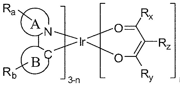
- M is a metal of atomic weight higher than 40; wherein A and B are each independently a 5 or 6-membered aromatic or heteroaromatic ring, and A-B represents a bonded pair of aromatic or heteroaromatic rings coordinated to the metal via a nitrogen atom on ring A and an sp 2 hybridized carbon atom on ring B; wherein R 3 , Rb, R x , Ry, R z are each independently selected from the group consisting of no substitution, alkyl, heteroalkyl, aryl, or heteroaryl groups; wherein each of R 3 and R b represent one or more substituents; wherein at least one of R x and R y contains a branched alkyl moiety with branching at a position further than the ⁇ position to the carbonyl group; wherein m is the oxidation state of the metal; and wherein n is at least 1.
- the compound can be or
- R x and R y can an isobutyl group.
- R z can be hydrogen.
- Specific exemplary compounds are also provided, e.g., Compounds 3 and 5-7.
- An organic light emitting device comprises an anode, a cathode, and an organic layer disposed between the anode and the cathode.
- the organic layer comprises one or more of the inventive compounds.
- the organic layer can be an emissive layer that contains an emissive dopant and a host, wherein the inventive compound is the emissive dopant and BAIq is the host.
- a consumer product is also provided.
- the consumer product comprises a device which itself comprises an anode, a cathode, and an organic layer disposed between the anode and the cathode.
- the organic layer comprises one or more of the inventive compounds.
- a method comprising reacting with R 7 -X to form
- organometallic compound is also provided, the organometallic compound containing a structure selected from the group consisting of:
- FIG. 1 shows an organic light emitting device.
- FIG. 2 shows an inverted organic light emitting device that does not have a separate electron transport layer.
- FIG. 3 shows an example of an indium compound.
- an OLED comprises at least one organic layer disposed between and electrically connected to an anode and a cathode.
- the anode injects holes and the cathode injects electrons into the organic layer(s).
- the injected holes and electrons each migrate toward the oppositely charged electrode.
- an "exciton” which is a localized electron-hole pair having an excited energy state, is formed.
- Light is emitted when the exciton relaxes via a photoemissive mechanism.
- the exciton may be localized on an excimer or an exciplex. Non- radiative mechanisms, such as thermal relaxation, may also occur, but are generally considered undesirable.
- the initial OLEDs used emissive molecules that emitted light from their singlet states ("fluorescence") as disclosed, for example, in U.S. Pat. No. 4,769,292, which is incorporated by reference in its entirety. Fluorescent emission generally occurs in a time frame of less than 10 nanoseconds.
- FIG. 1 shows an organic light emitting device 100.
- Device 100 may include a substrate 110, an anode 115, a hole injection layer 120, a hole transport layer 125, an electron blocking layer 130, an emissive layer 135, a hole blocking layer 140, an electron transport layer 145, an electron injection layer 150, a protective layer 155, and a cathode 160.
- Cathode 160 is a compound cathode having a first conductive layer 162 and a second conductive layer 164.
- Device 100 may be fabricated by depositing the layers described, in order. The properties and functions of these various layers, as well as example materials, are described in more detail in US 7,279,704 at cols. 6- 10, which are incorporated by reference.
- each of these layers are available.
- a flexible and transparent substrate-anode combination is disclosed in U.S. Pat. No. 5,844,363, which is incorporated by reference in its entirety.
- An example of a p-doped hole transport layer is m- MTDATA doped with F.sub.4-TCNQ at a molar ratio of 50:1, as disclosed in U.S. Patent Application Publication No. 2003/0230980, which is incorporated by reference in its entirety.
- Examples of emissive and host materials are disclosed in U.S. Pat. No. 6,303,238 to Thompson et al., which is incorporated by reference in its entirety.
- n- doped electron transport layer is BPhen doped with Li at a molar ratio of 1 :1, as disclosed in U.S. Patent Application Publication No. 2003/0230980, which is incorporated by reference in its entirety.
- Mg metal
- ITO overlying transparent, electrically-conductive, sputter- deposited ITO layer.
- FIG. 2 shows an inverted OLED 200.
- the device includes a substrate 210, a cathode 215, an emissive layer 220, a hole transport layer 225, and an anode 230.
- Device 200 may be fabricated by depositing the layers described, in order. Because the most common OLED configuration has a cathode disposed over the anode, and device 200 has cathode 215 disposed under anode 230, device 200 may be referred to as an "inverted" OLED. Materials similar to those described with respect to device 100 may be used in the corresponding layers of device 200.
- FIG. 2 provides one example of how some layers may be omitted from the structure of device 100.
- FIGS. 1 and 2 The simple layered structure illustrated in FIGS. 1 and 2 is provided by way of non- limiting example, and it is understood that embodiments of the invention may be used in connection with a wide variety of other structures.
- the specific materials and structures described are exemplary in nature, and other materials and structures may be used.
- Functional OLEDs may be achieved by combining the various layers described in different ways, or layers may be omitted entirely, based on design, performance, and cost factors. Other layers not specifically described may also be included. Materials other than those specifically described may be used. Although many of the examples provided herein describe various layers as comprising a single material, it is understood that combinations of materials, such as a mixture of host and dopant, or more generally a mixture, may be used. Also, the layers may have various sublayers.
- hole transport layer 225 transports holes and injects holes into emissive layer 220, and may be described as a hole transport layer or a hole injection layer.
- an OLED may be described as having an "organic layer" disposed between a cathode and an anode. This organic layer may comprise a single layer, or may further comprise multiple layers of different organic materials as described, for example, with respect to FIGS. 1 and 2.
- OLEDs comprised of polymeric materials (PLEDs) such as disclosed in U.S. Pat. No. 5,247,190 to Friend et al., which is incorporated by reference in its entirety.
- PLEDs polymeric materials
- OLEDs having a single organic layer may be used.
- OLEDs may be stacked, for example as described in U.S. Pat. No. 5,707,745 to Forrest et al, which is incorporated by reference in its entirety.
- the OLED structure may deviate from the simple layered structure illustrated in FIGS. 1 and 2.
- the substrate may include an angled reflective surface to improve out-coupling, such as a mesa structure as described in U.S. Pat. No. 6,091,195 to Forrest et al., and/or a pit structure as described in U.S. Pat. No. 5,834,893 to Bulovic et al., which are incorporated by reference in their entireties.
- any of the layers of the various embodiments may be deposited by any suitable method.
- preferred methods include thermal evaporation, ink-jet, such as described in U.S. Pat. Nos. 6,013,982 and 6,087,196, which are incorporated by reference in their entireties, organic vapor phase deposition (OVPD), such as described in U.S. Pat. No. 6,337,102 to Forrest et al., which is incorporated by reference in its entirety, and deposition by organic vapor jet printing (OVJP), such as described in U.S. patent application Ser. No. 10/233,470, which is incorporated by reference in its entirety.
- OVPD organic vapor phase deposition
- OJP organic vapor jet printing
- Other suitable deposition methods include spin coating and other solution based processes.
- Solution based processes are preferably carried out in nitrogen or an inert atmosphere.
- preferred methods include thermal evaporation.
- Preferred patterning methods include deposition through a mask, cold welding such as described in U.S. Pat. Nos. 6,294,398 and 6,468,819, which are incorporated by reference in their entireties, and patterning associated with some of the deposition methods such as ink-jet and OVJD. Other methods may also be used.
- the materials to be deposited may be modified to make them compatible with a particular deposition method. For example, substituents such as alkyl and aryl groups, branched or unbranched, and preferably containing at least 3 carbons, may be used in small molecules to enhance their ability to undergo solution processing.
- Substituents having 20 carbons or more may be used, and 3-20 carbons is a preferred range. Materials with asymmetric structures may have better solution processibility than those having symmetric structures, because asymmetric materials may have a lower tendency to recrystallize. Dendrimer substituents may be used to enhance the ability of small molecules to undergo solution processing.
- Devices fabricated in accordance with embodiments of the invention may be incorporated into a wide variety of consumer products, including flat panel displays, computer monitors, televisions, billboards, lights for interior or exterior illumination and/or signaling, heads up displays, fully transparent displays, flexible displays, laser printers, telephones, cell phones, personal digital assistants (PDAs), laptop computers, digital cameras, camcorders, viewfinders, micro-displays, vehicles, a large area wall, theater or stadium screen, or a sign.
- PDAs personal digital assistants
- Various control mechanisms may be used to control devices fabricated in accordance with the present invention, including passive matrix and active matrix. Many of the devices are intended for use in a temperature range comfortable to humans, such as 18 degrees C. to 30 degrees C, and more preferably at room temperature (20-25 degrees C).
- the materials and structures described herein may have applications in devices other than OLEDs.
- other optoelectronic devices such as organic solar cells and organic photodetectors may employ the materials and structures.
- organic devices such as organic transistors, may employ the materials and structures.
- halo halogen, alkyl, cycloalkyl, alkenyl, alkynyl, arylkyl, heterocyclic group, aryl, aromatic group, and heteroaryl are known to the art, and are defined in US 7,279,704 at cols. 31-32, which are incorporated herein by reference.
- Ir(2-phenylquinoline) and Ir(l-phenylisoquinoline) type phosphorescent materials have been synthesized, and OLEDs incorporating them as the dopant emitters have been fabricated.
- the devices may exhibit advantageously exhibit high current efficiency, high stability, narrow emission, improved processibility (e.g., high solubility and low sublimation temperature), and/or high luminous efficiency: quantum efficiency ratio (LE:EQE).
- M is a metal of atomic weight higher than 40; wherein A and B are each independently a 5 or 6-membered aromatic or heteroaromatic ring, and A-B represents a bonded pair of aromatic or heteroaromatic rings coordinated to the metal via a nitrogen atom on ring A and an sp2 hybridized carbon atom on ring B; wherein Ra, Rb, Rx, Ry, Rz are each independently selected from the group consisting of no substitution, alkyl, heteroalkyl, aryl, or heteroaryl groups; wherein each of R a and R b represent one or more substituents and can join to form fused rings; wherein at least one of R x and R y contains a branched alkyl moiety with branching at a position further than the ⁇ position to the carbonyl group; wherein m is the oxidation state of the metal; and wherein n is an integer less than m and at least 1.
- the compound may have the formula:
- the bonded pair of aromatic or heteroaromatic rings present in the compound, represented by A-B, is selected from the group consisting of:
- X is N-R, O or S; and wherein R is selected from
- the compound may have the formula:
- R x and R y are an isobutyl group.
- R z is hydrogen.
- Exemplary compounds include compound that are selected from the group consisting of:
- Such a compound includes
- the compounds described herein provide high device efficiency and stability, and a very narrow spectrum among other desirable properties. It is thought that a branched substituents at least at one of R x and R y , in combination with the methyl substituents on the phenyl ring (ring B) of the compound may provide for the very narrow emission spectrum and other remarkably good properties of the compound.
- An organic light emitting device comprises an anode, a cathode, and an organic layer that is disposed between the anode and the cathode.
- the organic layer further comprising a compound having the formula: wherein M is a metal of atomic weight higher than 40; wherein A and B are each independently a 5 or 6-membered aromatic or heteroaromatic ring, and A-B represents a bonded pair of aromatic or heteroaromatic rings coordinated to the metal via a nitrogen atom on ring A and an sp 2 hybridized carbon atom on ring B; wherein R 3 , R b , R x , R y , R 2 are each independently selected from the group consisting of no substitution, alkyl, heteroalkyl, aryl, or heteroaryl groups; wherein each of R a and R b represent one or more substituents; wherein at least one of R x and R y contains a branched alkyl moiety with branching at a position
- the device can contain the compound
- the device can contain a compound wherein A-B of the compound is selected from the group consisting of:
- the device can contain a compound having the formula:
- the device can contain a compound wherein R x and R y are an isobutyl group.
- the device can contain a compound wherein R 2 is hydrogen.
- the device can contain a compound selected from the group consisting of:
- the device can contain a compound wherein R z is methyl.
- the device can contain the compound [0055]
- the organic layer of the device is an emissive layer comprising the compound and a host.
- the compound is the emissive material.
- the host is a metal coordination complex.
- the host material can be BAIq.
- the compound of the device is the emissive material and the host is a metal coordination complex.
- the host material can be BAIq.
- an organic light emitting device comprises an anode, a cathode, and an organic layer disposed between the anode and the cathode, the organic layer comprising a compound selected from the group consisting of:
- the organic later of the device can be an emissive layer comprising the compound and a host.
- the inventive compound can be the emissive material and the host can be a metal coordination complex.
- the host can be BAIq.
- a consumer product comprising a device, the device further comprising an anode, a cathode, and an organic layer disposed between the anode and the cathode.
- the organic layer further comprising a compound having the formula:
- M is a metal of atomic weight higher than 40; wherein A and B are each independently a 5 or 6-membered aromatic or heteroaromatic ring, and A-B represents a bonded pair of aromatic or heteroaromatic rings coordinated to the metal via a nitrogen atom on ring A and an sp 2 hybridized carbon atom on ring B; wherein R a , R b , R x , R y , R 2 are each independently selected from the group consisting of no substitution, alkyl, heteroalkyl, aryl, or heteroaryl groups; wherein each of R a and R b represent one or more substituents; wherein at least one of R x and R y contains a branched alkyl moiety with branching at a position further than the ⁇ position to the carbonyl group; wherein m is the oxidation state of the metal; and wherein n is at least 1.
- a consumer device wherein the consumer product comprises a device, the device further comprising an anode, a cathode, and an organic layer disposed between the anode and the cathode.
- the organic layer further comprising a compound selected from the group consisting of:
- the method can further comprise reacting with a metal M and one or more ligands to form a compound having the formula:
- M is a metal of atomic weight higher than 40; wherein A and B are each independently a 5 or 6-membered aromatic or heteroaromatic ring, and A-B represents a bonded pair of aromatic or heteroaromatic rings coordinated to the metal via a nitrogen atom on ring A and an sp 2 hybridized carbon atom on ring B; wherein R A and R B each represent no substitution or one or more substituents; wherein each substituent of R A and R B is independently selected from the group consisting of alkyl, heteroalkyl, aryl, or heteroaryl groups; wherein m is the oxidation state of the metal; and wherein n is an integer less than m and at least 1.
- the method can further comprise wherein R z is a methyl group; and
- Isotopic analogues of the compounds provided herein where hydrogen has been replaced by deuterium are also included.
- organometallic compound contains a structure selected from the group consisting of
- the organometallic compound provided can have M as Ir.
- the organometallic compound provided can be a phosphorescent material.
- the materials described herein as useful for a particular layer in an organic light emitting device may be used in combination with a wide variety of other materials present in the device.
- emissive dopants disclosed herein may be used in conjunction with a wide variety of hosts, transport layers, blocking layers, injection layers, electrodes and other layers that may be present.
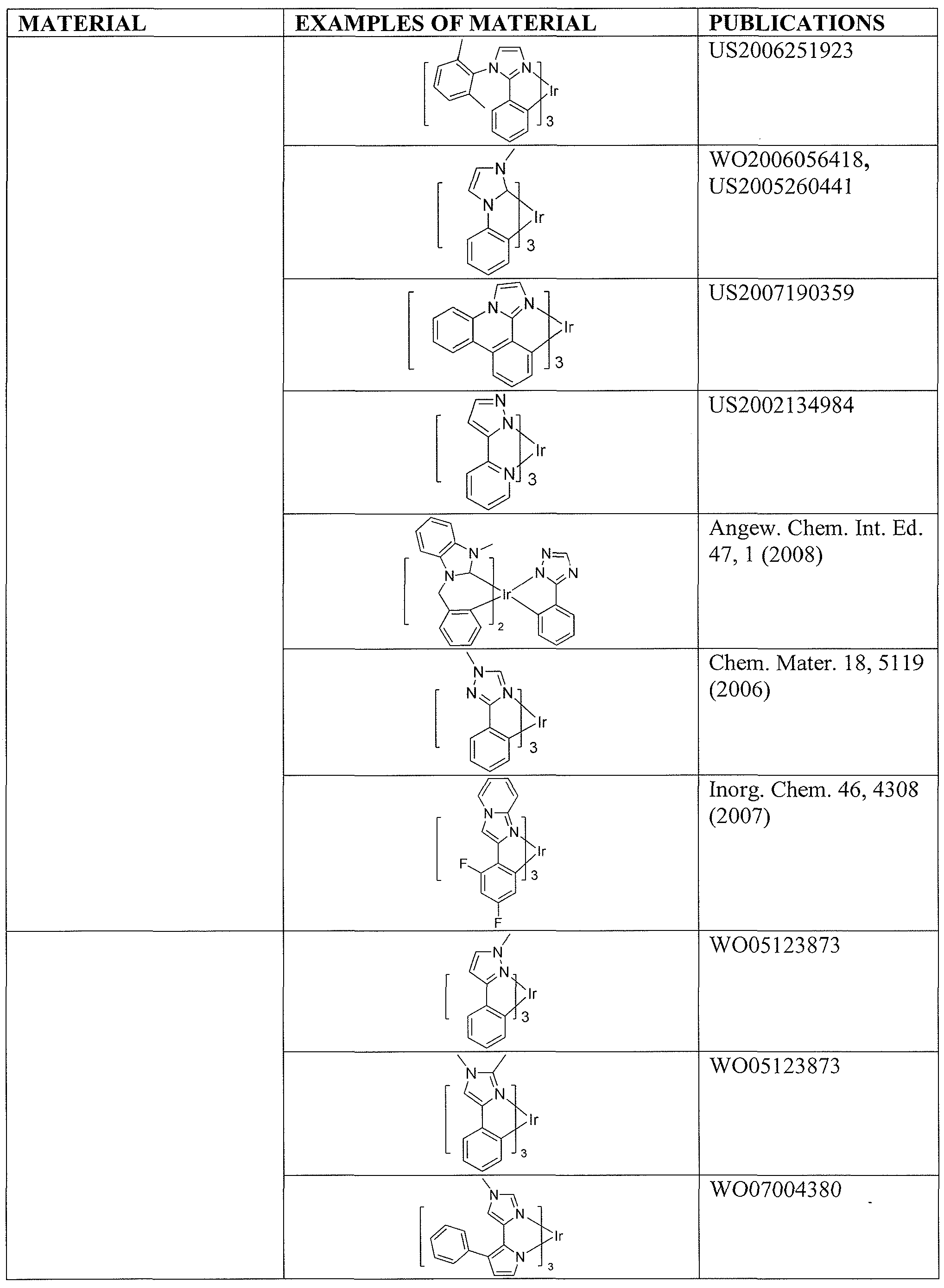
- the materials described or referred to below are non-limiting examples of materials that may be useful in combination with the compounds disclosed herein, and one of skill in the art can readily consult the literature to identify other materials that may be useful in combination.
- hole injection materials In addition to and / or in combination with the materials disclosed herein, many hole injection materials, hole transporting materials, host materials, dopant materials, exiton/hole blocking layer materials, electron transporting and electron injecting materials may be used in an OLED.
- Non-limiting examples of the materials that may be used in an OLED in combination with materials disclosed herein are listed in Table 1 below. Table 1 lists non- limiting classes of materials, non-limiting examples of compounds for each class, and references that disclose the materials.
- the product was extracted with ethyl acetate, washed with water, and dried over anhydrous magnesium sulfate.
- the product was purified using silica gel chromatography (5-15% ethyl acetate in hexane as eluent) to give a light yellow oil(85% yield). Further purification was done via vacuum distillation
- step 2 The reactor contents from step 2 were cooled to anmbient. 2,4-pentanedione (14.Og 140 mmol) and sodium carbonate (30.0g, 280mmol) were added to the reactor. The reaction mixture was stirred at ambient for 24h. 5g of celite and 50OmL of dichloromethane was added to the reaction mixture to dissolve the product. The mixture was then filtered through a bed of celite. The filtrate was then passed through a through a silica/alumina plug and washed with dichloromethane. The clarified solution was then filtered through GF/F filter paper the filtrate was heated to remove most of the dichloromethane.
- N 5 N dimethylformamide (DMF) (1 L) and potassium tert-butoxide(l 35.0g 1.2mol) were heated to 50C under nitrogen.
- Methyl 3-methylbutanoate (86.Og, 0.75mol) was added dropwise from a dropping funnel followed by a solution of 4-methylpentane-2-one(50g, lmol ) in 10OmL DMF.
- the progress of the reacrtion ws monitored by GC.
- the reaction was completed, the mixture was cooled to ambient and slowly neutralized with 20% H2SO4 solution. Water (30OmL) was added and two layers formed. The layer containing the 2,8- dimethylnonane-4,6-dione was purified using vacuum distillation to give 4Og of a pink oil (43% yield)
- step 4 The reactor contents from step 4 were cooled to anmbient. 2,4-pentanedione (14.Og 140 mmol) and sodium carbonate (30.0g, 280mmol) were added to the reactor. The reaction mixture was stirred at ambient for 24h. 5g of celite and 50OmL of dichloromethane was added to the reaction mixture to dissolve the product. The mixture was then filtered through a bed of celite. The filtrate was then passed through a through a silica/alumina plug and washed with dichloromethane. The clarified solution was then filtered through GF/F filter paper the filtrate was heated to remove most of the dichloromethane.
- N-(4-chlorophenylethyl)benzamide (15g, 52mmol), isobutylboronic acid (10.6g, 104mmol), Pd 2 (dba) 3 (lmol%), 2-dicyclohexylphosphino-2',6'-dimethoxybiphenyl (4 mol%), potassium phosphate monohydrate(22.0g 212mmol) 200ml of toluene was charged in a 25OmL round bottom flask. Nitrogen was bubbled through the reaction mixture for 20 minutes and heated to reflux for 18h overnight. The reaction mixture was allowed to cool to ambient temperature and the crude product was purified by column chromatography using 2% ethyl acetate in hexanes as solvent. 15g of desired product was obtained (93%yield).
- N-(4-p-isobutylphenylethyl)benzamide (15.Og), phosphorous pentoxide (5Og) phosphorous oxychloride 5OmL and xylenes (16OmL) was refluxed for 3 h in a IL round bottom flask. After the reaction mixture was allowed to cool to room temperature, the solvent was decanted and ice was slowly added to the solid in the bottom of the flask. The water-residue mixture was made weakly alkaline with 50% NaOH and the product was extracted with toluene. The organic layer was washed with water and dried over anhydrous MgSO 4 . The solvent was evaporated to give 12.4g of crude product (88% yield) which was used without further purification.
- N-(4-p-isopropylphenylethyl)benzamide (7.5g) in 8OmL xylenes was refluxed for 3 hrs together with 25g phosphorous pentoxide and 25mL phosphorous oxychloride. After cooling, the solvent was decanted and ice was slowly added to the solid in the bottom of the flask. The water-residue mixture was made weakly alkaline with 50% NaOH and the product was extracted with toluene. The organic layer was washed with water and dried over anhydrousMgSO 4 . The solvent was removed under vacuum to give 6.2g of crude product which was used without further purification.
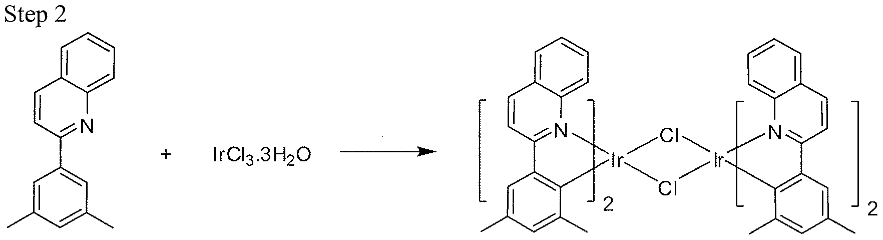
- Compound 9 can be synthesized using the same procedure as outlined for invention compound 7. In this case the dichlorobridged indium dimer that is formed should be cleaved with 2,4-pentane dione to afford the product.
- Compound 10 can be synthesized using the same procedure as outlined for invention compound 6. In this case the dichlorobridged iridium dimer that is formed should be cleaved with 2,4-pentane dione to afford the product.
- All device examples were fabricated by high vacuum ( ⁇ 1CT 7 Torr) thermal evaporation.
- the anode electrode is 1200A of indium tin oxide (ITO).
- the cathode consisted of IOA of LiF followed by IOOOA of Al. All devices were encapsulated with a glass lid sealed with an epoxy resin in a nitrogen glove box ( ⁇ 1 ppm of H 2 O and O 2 ) immediately after fabrication, and a moisture getter was incorporated inside the package.
- HIL hole injection layer
- EML emissive layer
- AIq 3 tris-8-hydroxyquinoline aluminum
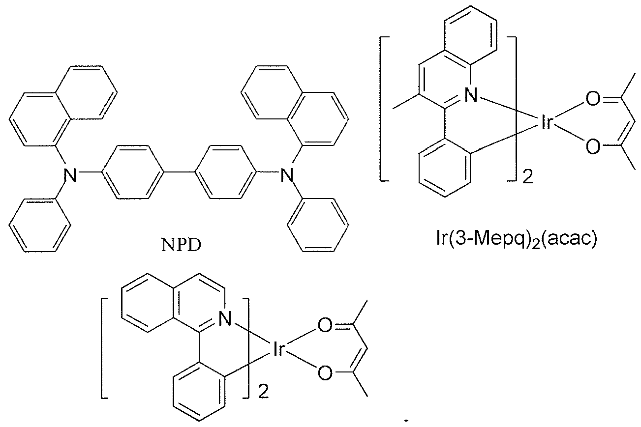
- Comparative Examples 1 and 2 were fabricated similarly to the Device Examples, except that Ir(3-Mepq) 2 (acac) or Ir(piq) 2 (acac) was used as the emissive dopant.
- the Device Examples containing inventive compounds show similar or higher device efficiency and lifetime and also extremely narrow emission spectra versus the Comparative Examples containing Ir(3-Mepq) 2 (acac) or Ir(piq) 2 (acac).
- the LE and EQE of Example 3 are 21.1 cd/A and 18.2% respectively, at CIE of (0.662, 0.335).
- the LE and EQE of Example 4 are 18.7 cd/A and 11.4% respectively, at CIE of (0.666, 0.331).
- the Full Width Half Max (FWHM) of the EL for examples 3, 4, 6 and 7 are 59, 61 , 55 and 55nm respectively. These are by far narrower than the EL measured for Comparative Examples 1 and 2 with FWHM 94 and 84nm, respectively.
- Device Examples 6 and 7 have the narrowest FWHM of any red indium complex reported to date. Therefore, the inventive compounds may be advantageously used in devices to improve efficiency, stability and luminescence.
- the sublimation temperatures using the branched diketone ligand, for example, Compounds 3, 6 and 7, are also quite low which are well suited for long term thermal evaporation required in manufacturing.
- the 70 0 C lifetime comparison shows that Device Example 8 is more stable than both Comparative Example 1 and 2. Therefore, the inventive compounds may be advantageously used in devices to improve device lifetime.
Abstract
Description


Claims


Priority Applications (8)
| Application Number | Priority Date | Filing Date | Title |
|---|---|---|---|
| CN2009801404917A CN102187491B (en) | 2008-09-16 | 2009-09-16 | Phosphorescent materials |
| KR1020157036659A KR20160005137A (en) | 2008-09-16 | 2009-09-16 | Phosphorescent materials |
| KR1020167031116A KR20160131127A (en) | 2008-09-16 | 2009-09-16 | Phosphorescent materials |
| JP2011527059A JP5878371B2 (en) | 2008-09-16 | 2009-09-16 | Phosphorescent substance |
| EP18180398.2A EP3404736B1 (en) | 2008-09-16 | 2009-09-16 | Organic light emitting diodes with phosphorescent materials |
| EP15191449.6A EP2999021B1 (en) | 2008-09-16 | 2009-09-16 | Phosphorescent materials |
| EP09792593.7A EP2329541B1 (en) | 2008-09-16 | 2009-09-16 | Phosphorescent materials |
| KR1020177019540A KR101974294B1 (en) | 2008-09-16 | 2009-09-16 | Phosphorescent materials |
Applications Claiming Priority (2)
| Application Number | Priority Date | Filing Date | Title |
|---|---|---|---|
| US9748808P | 2008-09-16 | 2008-09-16 | |
| US61/097,488 | 2008-09-16 |
Publications (1)
| Publication Number | Publication Date |
|---|---|
| WO2010033550A1 true WO2010033550A1 (en) | 2010-03-25 |
Family
ID=41180009
Family Applications (1)
| Application Number | Title | Priority Date | Filing Date |
|---|---|---|---|
| PCT/US2009/057098 WO2010033550A1 (en) | 2008-09-16 | 2009-09-16 | Phosphorescent materials |
Country Status (7)
| Country | Link |
|---|---|
| US (2) | US9034483B2 (en) |
| EP (3) | EP3404736B1 (en) |
| JP (4) | JP5878371B2 (en) |
| KR (4) | KR20160131127A (en) |
| CN (2) | CN102187491B (en) |
| TW (2) | TWI555734B (en) |
| WO (1) | WO2010033550A1 (en) |
Cited By (17)
| Publication number | Priority date | Publication date | Assignee | Title |
|---|---|---|---|---|
| JP2013035822A (en) * | 2011-08-05 | 2013-02-21 | Industrial Technology Research Inst | Organometallic compound and organic electroluminescence device employing the same |
| JP2013142088A (en) * | 2012-01-06 | 2013-07-22 | Universal Display Corp | Highly efficient phosphorescent material |
| US20130306961A1 (en) * | 2011-02-11 | 2013-11-21 | Idemitsu Kosen Co. Ltd | Organic light emitting device and materials for use in same |
| JP2013543864A (en) * | 2010-11-11 | 2013-12-09 | ユニバーサル ディスプレイ コーポレイション | Phosphorescent substance |
| JP2014511025A (en) * | 2011-02-11 | 2014-05-01 | ユニバーサル ディスプレイ コーポレイション | ORGANIC LIGHT EMITTING DEVICE AND MATERIAL FOR USE IN THE ORGANIC LIGHT EMITTING DEVICE |
| US9163174B2 (en) | 2012-01-04 | 2015-10-20 | Universal Display Corporation | Highly efficient phosphorescent materials |
| KR20160054390A (en) | 2014-11-06 | 2016-05-16 | 롬엔드하스전자재료코리아유한회사 | Organic electroluminescent compound and organic electroluminescent device comprising the same |
| KR20160059437A (en) | 2014-11-18 | 2016-05-26 | 롬엔드하스전자재료코리아유한회사 | A plurality of dopant materials and organic electroluminescent device comprising the same |
| EP2602302B1 (en) * | 2011-12-09 | 2016-06-29 | Universal Display Corporation | Novel organic light emitting materials |
| US9978960B2 (en) | 2013-06-14 | 2018-05-22 | Semiconductor Energy Laboratory Co., Ltd. | Organometallic iridium complex, light-emitting element, light-emitting device, and lighting device |
| US10084143B2 (en) | 2008-09-16 | 2018-09-25 | Universal Display Corporation | Phosphorescent materials |
| US10199581B2 (en) | 2013-07-01 | 2019-02-05 | Universal Display Corporation | Organic electroluminescent materials and devices |
| CN109952358A (en) * | 2016-12-07 | 2019-06-28 | 罗门哈斯电子材料韩国有限公司 | Electroluminescent organic material and Organnic electroluminescent device comprising it |
| EP3549944A1 (en) * | 2018-04-02 | 2019-10-09 | Samsung Electronics Co., Ltd. | Organometallic compound, organic light-emitting device including the same, and diagnostic composition including the organometallic compound |
| JP2020503672A (en) * | 2016-12-27 | 2020-01-30 | ローム・アンド・ハース・エレクトロニック・マテリアルズ・コリア・リミテッド | Organic electroluminescent compound and organic electroluminescent device containing the same |
| US11459348B2 (en) | 2018-04-02 | 2022-10-04 | Samsung Electronics Co., Ltd. | Organometallic compound, organic light-emitting device including the same, and diagnostic composition including the organometallic compound |
| KR20230070192A (en) | 2014-11-04 | 2023-05-22 | 롬엔드하스전자재료코리아유한회사 | A Novel Combination of a Host Compound and a Dopant Compound and an Organic Electroluminescent Device Comprising the Same |
Families Citing this family (97)
| Publication number | Priority date | Publication date | Assignee | Title |
|---|---|---|---|---|
| EP2399922B1 (en) | 2006-02-10 | 2019-06-26 | Universal Display Corporation | Metal complexes of cyclometallated imidazo(1,2-f) phenanthridine and diimidazo(1,2-A;1',2'-C)quinazoline ligands and isoelectronic and benzannulated analogs therof |
| US9130177B2 (en) | 2011-01-13 | 2015-09-08 | Universal Display Corporation | 5-substituted 2 phenylquinoline complexes materials for light emitting diode |
| CN101657518A (en) * | 2007-03-08 | 2010-02-24 | 通用显示公司 | phosphorescent materials |
| US8288187B2 (en) | 2010-01-20 | 2012-10-16 | Universal Display Corporation | Electroluminescent devices for lighting applications |
| US10008677B2 (en) * | 2011-01-13 | 2018-06-26 | Universal Display Corporation | Materials for organic light emitting diode |
| US8748012B2 (en) | 2011-05-25 | 2014-06-10 | Universal Display Corporation | Host materials for OLED |
| US9386657B2 (en) | 2012-03-15 | 2016-07-05 | Universal Display Corporation | Organic Electroluminescent materials and devices |
| KR20150030660A (en) * | 2012-06-14 | 2015-03-20 | 유니버셜 디스플레이 코포레이션 | Biscarbazole derivative host materials and red emitter for oled emissive region |
| US9540329B2 (en) | 2012-07-19 | 2017-01-10 | Universal Display Corporation | Organic electroluminescent materials and devices |
| US9252363B2 (en) | 2012-10-04 | 2016-02-02 | Universal Display Corporation | Aryloxyalkylcarboxylate solvent compositions for inkjet printing of organic layers |
| US9196860B2 (en) | 2012-12-04 | 2015-11-24 | Universal Display Corporation | Compounds for triplet-triplet annihilation upconversion |
| US8716484B1 (en) | 2012-12-05 | 2014-05-06 | Universal Display Corporation | Hole transporting materials with twisted aryl groups |
| US9653691B2 (en) | 2012-12-12 | 2017-05-16 | Universal Display Corporation | Phosphorescence-sensitizing fluorescence material system |
| US9876173B2 (en) | 2013-12-09 | 2018-01-23 | Universal Display Corporation | Organic electroluminescent materials and devices |
| KR20150094127A (en) * | 2014-02-10 | 2015-08-19 | 롬엔드하스전자재료코리아유한회사 | An Organic Electroluminescent Device |
| US10003033B2 (en) * | 2014-02-18 | 2018-06-19 | Universal Display Corporation | Organic electroluminescent materials and devices |
| US9450198B2 (en) | 2014-04-15 | 2016-09-20 | Universal Display Corporation | Organic electroluminescent materials and devices |
| KR102308903B1 (en) * | 2014-06-17 | 2021-10-06 | 삼성디스플레이 주식회사 | Organic light emitting device |
| KR102241847B1 (en) * | 2014-07-29 | 2021-04-20 | 삼성디스플레이 주식회사 | Organic light emitting device |
| CN104193783B (en) * | 2014-07-31 | 2017-05-17 | 石家庄诚志永华显示材料有限公司 | Benzoisoquinoline metal complex as well as preparation method and application thereof |
| US9929361B2 (en) | 2015-02-16 | 2018-03-27 | Universal Display Corporation | Organic electroluminescent materials and devices |
| US11056657B2 (en) | 2015-02-27 | 2021-07-06 | University Display Corporation | Organic electroluminescent materials and devices |
| US9859510B2 (en) | 2015-05-15 | 2018-01-02 | Universal Display Corporation | Organic electroluminescent materials and devices |
| US10418568B2 (en) | 2015-06-01 | 2019-09-17 | Universal Display Corporation | Organic electroluminescent materials and devices |
| US11127905B2 (en) | 2015-07-29 | 2021-09-21 | Universal Display Corporation | Organic electroluminescent materials and devices |
| US10672996B2 (en) | 2015-09-03 | 2020-06-02 | Universal Display Corporation | Organic electroluminescent materials and devices |
| US20170229663A1 (en) | 2016-02-09 | 2017-08-10 | Universal Display Corporation | Organic electroluminescent materials and devices |
| US10236456B2 (en) | 2016-04-11 | 2019-03-19 | Universal Display Corporation | Organic electroluminescent materials and devices |
| US10862054B2 (en) | 2016-06-20 | 2020-12-08 | Universal Display Corporation | Organic electroluminescent materials and devices |
| US10672997B2 (en) | 2016-06-20 | 2020-06-02 | Universal Display Corporation | Organic electroluminescent materials and devices |
| US11482683B2 (en) | 2016-06-20 | 2022-10-25 | Universal Display Corporation | Organic electroluminescent materials and devices |
| US10608186B2 (en) | 2016-09-14 | 2020-03-31 | Universal Display Corporation | Organic electroluminescent materials and devices |
| US10680187B2 (en) | 2016-09-23 | 2020-06-09 | Universal Display Corporation | Organic electroluminescent materials and devices |
| US11196010B2 (en) | 2016-10-03 | 2021-12-07 | Universal Display Corporation | Organic electroluminescent materials and devices |
| US11011709B2 (en) | 2016-10-07 | 2021-05-18 | Universal Display Corporation | Organic electroluminescent materials and devices |
| US20180130956A1 (en) | 2016-11-09 | 2018-05-10 | Universal Display Corporation | Organic electroluminescent materials and devices |
| US10680188B2 (en) | 2016-11-11 | 2020-06-09 | Universal Display Corporation | Organic electroluminescent materials and devices |
| US11780865B2 (en) | 2017-01-09 | 2023-10-10 | Universal Display Corporation | Organic electroluminescent materials and devices |
| US10686146B2 (en) * | 2017-02-13 | 2020-06-16 | Feng-wen Yen | Paracyclophane-based iridium complexes for organic electroluminescence device |
| US10844085B2 (en) | 2017-03-29 | 2020-11-24 | Universal Display Corporation | Organic electroluminescent materials and devices |
| US10944060B2 (en) | 2017-05-11 | 2021-03-09 | Universal Display Corporation | Organic electroluminescent materials and devices |
| US20180370999A1 (en) | 2017-06-23 | 2018-12-27 | Universal Display Corporation | Organic electroluminescent materials and devices |
| US11228010B2 (en) | 2017-07-26 | 2022-01-18 | Universal Display Corporation | Organic electroluminescent materials and devices |
| US11744142B2 (en) | 2017-08-10 | 2023-08-29 | Universal Display Corporation | Organic electroluminescent materials and devices |
| US20190161504A1 (en) | 2017-11-28 | 2019-05-30 | University Of Southern California | Carbene compounds and organic electroluminescent devices |
| EP3492480B1 (en) | 2017-11-29 | 2021-10-20 | Universal Display Corporation | Organic electroluminescent materials and devices |
| US11937503B2 (en) | 2017-11-30 | 2024-03-19 | Universal Display Corporation | Organic electroluminescent materials and devices |
| US20190194234A1 (en) * | 2017-12-25 | 2019-06-27 | Chuanjun Xia | Metal complexes containing heterocycle substituted ligands, and electroluminescent devices and formulations containing the complexes |
| US11542289B2 (en) | 2018-01-26 | 2023-01-03 | Universal Display Corporation | Organic electroluminescent materials and devices |
| KR102206820B1 (en) * | 2018-05-14 | 2021-01-22 | 주식회사 엘지화학 | Compound and organic light emitting device comprising the same |
| CN109053810A (en) * | 2018-07-12 | 2018-12-21 | 浙江福斯特新材料研究院有限公司 | Iridium organ metallic compound and organic electroluminescence device |
| EP3604321B1 (en) | 2018-07-31 | 2022-02-09 | Samsung Electronics Co., Ltd. | Organometallic compound, organic light-emitting device including the same, and diagnostic composition including the organometallic compound |
| CN109053813A (en) * | 2018-08-03 | 2018-12-21 | 瑞声科技(南京)有限公司 | A kind of feux rouges metal complex, preparation method and application |
| US20200075870A1 (en) | 2018-08-22 | 2020-03-05 | Universal Display Corporation | Organic electroluminescent materials and devices |
| CN110922429B (en) * | 2018-09-20 | 2023-11-03 | 北京夏禾科技有限公司 | Organic light-emitting material containing auxiliary ligand |
| US11737349B2 (en) | 2018-12-12 | 2023-08-22 | Universal Display Corporation | Organic electroluminescent materials and devices |
| US11780829B2 (en) | 2019-01-30 | 2023-10-10 | The University Of Southern California | Organic electroluminescent materials and devices |
| KR20200095395A (en) | 2019-01-31 | 2020-08-10 | 삼성전자주식회사 | Organometallic compound and organic light emitting device including the same |
| US20200251664A1 (en) | 2019-02-01 | 2020-08-06 | Universal Display Corporation | Organic electroluminescent materials and devices |
| JP2020158491A (en) | 2019-03-26 | 2020-10-01 | ユニバーサル ディスプレイ コーポレイション | Organic electroluminescent materials and devices |
| CN111909212B (en) | 2019-05-09 | 2023-12-26 | 北京夏禾科技有限公司 | Organic luminescent material containing 6-silicon-based substituted isoquinoline ligand |
| CN111909214B (en) | 2019-05-09 | 2024-03-29 | 北京夏禾科技有限公司 | Organic luminescent material containing 3-deuterium substituted isoquinoline ligand |
| CN111909213B (en) | 2019-05-09 | 2024-02-27 | 北京夏禾科技有限公司 | Metal complex containing three different ligands |
| CN111943986B (en) * | 2019-05-17 | 2023-08-15 | 夏禾科技(江苏)有限公司 | Metal complex containing multiple condensed heterocyclic structure ligands |
| US20210032278A1 (en) | 2019-07-30 | 2021-02-04 | Universal Display Corporation | Organic electroluminescent materials and devices |
| KR20210017822A (en) | 2019-08-09 | 2021-02-17 | 삼성전자주식회사 | Organometallic compound, organic light emitting device including the same and a composition for diagnosing including the same |
| US20210047354A1 (en) | 2019-08-16 | 2021-02-18 | Universal Display Corporation | Organic electroluminescent materials and devices |
| US20210135130A1 (en) | 2019-11-04 | 2021-05-06 | Universal Display Corporation | Organic electroluminescent materials and devices |
| US20210217969A1 (en) | 2020-01-06 | 2021-07-15 | Universal Display Corporation | Organic electroluminescent materials and devices |
| US20220336759A1 (en) | 2020-01-28 | 2022-10-20 | Universal Display Corporation | Organic electroluminescent materials and devices |
| EP3937268A1 (en) | 2020-07-10 | 2022-01-12 | Universal Display Corporation | Plasmonic oleds and vertical dipole emitters |
| JP2023541975A (en) | 2020-09-18 | 2023-10-04 | 三星ディスプレイ株式會社 | organic electroluminescent device |
| US20220158096A1 (en) | 2020-11-16 | 2022-05-19 | Universal Display Corporation | Organic electroluminescent materials and devices |
| US20220165967A1 (en) | 2020-11-24 | 2022-05-26 | Universal Display Corporation | Organic electroluminescent materials and devices |
| US20220162243A1 (en) | 2020-11-24 | 2022-05-26 | Universal Display Corporation | Organic electroluminescent materials and devices |
| US20220271241A1 (en) | 2021-02-03 | 2022-08-25 | Universal Display Corporation | Organic electroluminescent materials and devices |
| EP4059915A3 (en) | 2021-02-26 | 2022-12-28 | Universal Display Corporation | Organic electroluminescent materials and devices |
| EP4060758A3 (en) | 2021-02-26 | 2023-03-29 | Universal Display Corporation | Organic electroluminescent materials and devices |
| US20220298192A1 (en) | 2021-03-05 | 2022-09-22 | Universal Display Corporation | Organic electroluminescent materials and devices |
| US20220298190A1 (en) | 2021-03-12 | 2022-09-22 | Universal Display Corporation | Organic electroluminescent materials and devices |
| US20220298193A1 (en) | 2021-03-15 | 2022-09-22 | Universal Display Corporation | Organic electroluminescent materials and devices |
| US20220340607A1 (en) | 2021-04-05 | 2022-10-27 | Universal Display Corporation | Organic electroluminescent materials and devices |
| EP4075531A1 (en) | 2021-04-13 | 2022-10-19 | Universal Display Corporation | Plasmonic oleds and vertical dipole emitters |
| US20220352478A1 (en) | 2021-04-14 | 2022-11-03 | Universal Display Corporation | Organic eletroluminescent materials and devices |
| US20230006149A1 (en) | 2021-04-23 | 2023-01-05 | Universal Display Corporation | Organic electroluminescent materials and devices |
| US20220407020A1 (en) | 2021-04-23 | 2022-12-22 | Universal Display Corporation | Organic electroluminescent materials and devices |
| US20230133787A1 (en) | 2021-06-08 | 2023-05-04 | University Of Southern California | Molecular Alignment of Homoleptic Iridium Phosphors |
| KR20230038890A (en) | 2021-09-13 | 2023-03-21 | 롬엔드하스전자재료코리아유한회사 | Organic electroluminescent materials and organic electroluminescent device comprising the same |
| EP4151699A1 (en) | 2021-09-17 | 2023-03-22 | Universal Display Corporation | Organic electroluminescent materials and devices |
| EP4212539A1 (en) | 2021-12-16 | 2023-07-19 | Universal Display Corporation | Organic electroluminescent materials and devices |
| EP4231804A3 (en) | 2022-02-16 | 2023-09-20 | Universal Display Corporation | Organic electroluminescent materials and devices |
| US20230292592A1 (en) | 2022-03-09 | 2023-09-14 | Universal Display Corporation | Organic electroluminescent materials and devices |
| US20230337516A1 (en) | 2022-04-18 | 2023-10-19 | Universal Display Corporation | Organic electroluminescent materials and devices |
| US20230389421A1 (en) | 2022-05-24 | 2023-11-30 | Universal Display Corporation | Organic electroluminescent materials and devices |
| EP4293001A1 (en) | 2022-06-08 | 2023-12-20 | Universal Display Corporation | Organic electroluminescent materials and devices |
| US20240016051A1 (en) | 2022-06-28 | 2024-01-11 | Universal Display Corporation | Organic electroluminescent materials and devices |
| US20240107880A1 (en) | 2022-08-17 | 2024-03-28 | Universal Display Corporation | Organic electroluminescent materials and devices |
Citations (2)
| Publication number | Priority date | Publication date | Assignee | Title |
|---|---|---|---|---|
| KR100662430B1 (en) * | 2005-11-07 | 2007-01-02 | 엘지전자 주식회사 | Red phosphorescene compounds and organic electroluminescence devices using the same |
| US20070004918A1 (en) * | 2005-03-08 | 2007-01-04 | Lg Electronics Inc. | Red phosphorescence compounds and organic electroluminescence device using the same |
Family Cites Families (134)
| Publication number | Priority date | Publication date | Assignee | Title |
|---|---|---|---|---|
| US4769292A (en) * | 1987-03-02 | 1988-09-06 | Eastman Kodak Company | Electroluminescent device with modified thin film luminescent zone |
| GB8909011D0 (en) * | 1989-04-20 | 1989-06-07 | Friend Richard H | Electroluminescent devices |
| US5061569A (en) * | 1990-07-26 | 1991-10-29 | Eastman Kodak Company | Electroluminescent device with organic electroluminescent medium |
| DE69412567T2 (en) | 1993-11-01 | 1999-02-04 | Hodogaya Chemical Co Ltd | Amine compound and electroluminescent device containing it |
| US5707745A (en) * | 1994-12-13 | 1998-01-13 | The Trustees Of Princeton University | Multicolor organic light emitting devices |
| US5703436A (en) * | 1994-12-13 | 1997-12-30 | The Trustees Of Princeton University | Transparent contacts for organic devices |
| US6939625B2 (en) | 1996-06-25 | 2005-09-06 | Nôrthwestern University | Organic light-emitting diodes and methods for assembly and enhanced charge injection |
| US5844363A (en) * | 1997-01-23 | 1998-12-01 | The Trustees Of Princeton Univ. | Vacuum deposited, non-polymeric flexible organic light emitting devices |
| US6091195A (en) * | 1997-02-03 | 2000-07-18 | The Trustees Of Princeton University | Displays having mesa pixel configuration |
| US6013982A (en) * | 1996-12-23 | 2000-01-11 | The Trustees Of Princeton University | Multicolor display devices |
| US5834893A (en) * | 1996-12-23 | 1998-11-10 | The Trustees Of Princeton University | High efficiency organic light emitting devices with light directing structures |
| US6303238B1 (en) * | 1997-12-01 | 2001-10-16 | The Trustees Of Princeton University | OLEDs doped with phosphorescent compounds |
| US6337102B1 (en) * | 1997-11-17 | 2002-01-08 | The Trustees Of Princeton University | Low pressure vapor phase deposition of organic thin films |
| US6087196A (en) * | 1998-01-30 | 2000-07-11 | The Trustees Of Princeton University | Fabrication of organic semiconductor devices using ink jet printing |
| US6528187B1 (en) | 1998-09-08 | 2003-03-04 | Fuji Photo Film Co., Ltd. | Material for luminescence element and luminescence element using the same |
| US6097147A (en) * | 1998-09-14 | 2000-08-01 | The Trustees Of Princeton University | Structure for high efficiency electroluminescent device |
| US6830828B2 (en) * | 1998-09-14 | 2004-12-14 | The Trustees Of Princeton University | Organometallic complexes as phosphorescent emitters in organic LEDs |
| US6294398B1 (en) * | 1999-11-23 | 2001-09-25 | The Trustees Of Princeton University | Method for patterning devices |
| US6458475B1 (en) | 1999-11-24 | 2002-10-01 | The Trustee Of Princeton University | Organic light emitting diode having a blue phosphorescent molecule as an emitter |
| KR100377321B1 (en) | 1999-12-31 | 2003-03-26 | 주식회사 엘지화학 | Electronic device comprising organic compound having p-type semiconducting characteristics |
| US20020121638A1 (en) | 2000-06-30 | 2002-09-05 | Vladimir Grushin | Electroluminescent iridium compounds with fluorinated phenylpyridines, phenylpyrimidines, and phenylquinolines and devices made with such compounds |
| CN102041001B (en) | 2000-08-11 | 2014-10-22 | 普林斯顿大学理事会 | Organometallic compounds and emission-shifting organic electrophosphorescence |
| EP1348711B1 (en) | 2000-11-30 | 2018-06-13 | Canon Kabushiki Kaisha | Luminescent element and display |
| US6579630B2 (en) | 2000-12-07 | 2003-06-17 | Canon Kabushiki Kaisha | Deuterated semiconducting organic compounds used for opto-electronic devices |
| JP3812730B2 (en) * | 2001-02-01 | 2006-08-23 | 富士写真フイルム株式会社 | Transition metal complex and light emitting device |
| JP4307000B2 (en) | 2001-03-08 | 2009-08-05 | キヤノン株式会社 | Metal coordination compound, electroluminescent element and display device |
| JP4310077B2 (en) | 2001-06-19 | 2009-08-05 | キヤノン株式会社 | Metal coordination compound and organic light emitting device |
| DE60232415D1 (en) | 2001-06-20 | 2009-07-02 | Showa Denko Kk | LIGHT-EMITTING MATERIAL AND ORGANIC LUMINAIRE DIODE |
| US7071615B2 (en) * | 2001-08-20 | 2006-07-04 | Universal Display Corporation | Transparent electrodes |
| US7250226B2 (en) | 2001-08-31 | 2007-07-31 | Nippon Hoso Kyokai | Phosphorescent compound, a phosphorescent composition and an organic light-emitting device |
| US7431968B1 (en) | 2001-09-04 | 2008-10-07 | The Trustees Of Princeton University | Process and apparatus for organic vapor jet deposition |
| US6835469B2 (en) * | 2001-10-17 | 2004-12-28 | The University Of Southern California | Phosphorescent compounds and devices comprising the same |
| US7166368B2 (en) | 2001-11-07 | 2007-01-23 | E. I. Du Pont De Nemours And Company | Electroluminescent platinum compounds and devices made with such compounds |
| US6863997B2 (en) * | 2001-12-28 | 2005-03-08 | The Trustees Of Princeton University | White light emitting OLEDs from combined monomer and aggregate emission |
| KR100691543B1 (en) | 2002-01-18 | 2007-03-09 | 주식회사 엘지화학 | New material for transporting electron and organic electroluminescent display using the same |
| US20030230980A1 (en) * | 2002-06-18 | 2003-12-18 | Forrest Stephen R | Very low voltage, high efficiency phosphorescent oled in a p-i-n structure |
| CN100340630C (en) * | 2002-08-16 | 2007-10-03 | 南加利福尼亚大学 | Organic light emitting materials and devices |
| US7189989B2 (en) | 2002-08-22 | 2007-03-13 | Fuji Photo Film Co., Ltd. | Light emitting element |
| EP2264122A3 (en) | 2002-08-27 | 2011-05-11 | Fujifilm Corporation | Organometallic complexes, organic electroluminescent devices and organic electroluminescent displays |
| US6687266B1 (en) * | 2002-11-08 | 2004-02-03 | Universal Display Corporation | Organic light emitting materials and devices |
| JP4365196B2 (en) | 2002-12-27 | 2009-11-18 | 富士フイルム株式会社 | Organic electroluminescence device |
| JP4365199B2 (en) | 2002-12-27 | 2009-11-18 | 富士フイルム株式会社 | Organic electroluminescence device |
| KR100509603B1 (en) * | 2002-12-28 | 2005-08-22 | 삼성에스디아이 주식회사 | Red emitting compound and organic electroluminescence device |
| EP1606296B1 (en) | 2003-03-24 | 2009-08-05 | University Of Southern California | PHENYL-PYRAZOLE COMPLEXES OF Ir |
| US7090928B2 (en) | 2003-04-01 | 2006-08-15 | The University Of Southern California | Binuclear compounds |
| EP1717291A3 (en) | 2003-04-15 | 2007-03-21 | Merck Patent GmbH | Mixtures of matrix materials and organic semiconductors capable of emission, use of the same and electronic components containing said mixtures |
| US7029765B2 (en) * | 2003-04-22 | 2006-04-18 | Universal Display Corporation | Organic light emitting devices having reduced pixel shrinkage |
| US20060186791A1 (en) | 2003-05-29 | 2006-08-24 | Osamu Yoshitake | Organic electroluminescent element |
| JP2005011610A (en) | 2003-06-18 | 2005-01-13 | Nippon Steel Chem Co Ltd | Organic electroluminescent element |
| US20050025993A1 (en) * | 2003-07-25 | 2005-02-03 | Thompson Mark E. | Materials and structures for enhancing the performance of organic light emitting devices |
| TWI390006B (en) | 2003-08-07 | 2013-03-21 | Nippon Steel Chemical Co | Organic EL materials with aluminum clamps |
| DE10338550A1 (en) | 2003-08-19 | 2005-03-31 | Basf Ag | Transition metal complexes with carbene ligands as emitters for organic light-emitting diodes (OLEDs) |
| US20050260119A1 (en) * | 2003-09-09 | 2005-11-24 | Sunkara Mahendra K | Carbon nanopipettes methods of making and applications |
| US20060269780A1 (en) | 2003-09-25 | 2006-11-30 | Takayuki Fukumatsu | Organic electroluminescent device |
| JP4822687B2 (en) | 2003-11-21 | 2011-11-24 | 富士フイルム株式会社 | Organic electroluminescence device |
| US7332232B2 (en) | 2004-02-03 | 2008-02-19 | Universal Display Corporation | OLEDs utilizing multidentate ligand systems |
| KR100963457B1 (en) | 2004-03-11 | 2010-06-17 | 미쓰비시 가가꾸 가부시키가이샤 | Composition for charge-transporting film and ion compound, charge-transporting film and organic electroluminescent device using same, and method for manufacturing organic electroluminescent device and method for producing charge-transporting film |
| TW200531592A (en) | 2004-03-15 | 2005-09-16 | Nippon Steel Chemical Co | Organic electroluminescent device |
| JP4869565B2 (en) | 2004-04-23 | 2012-02-08 | 富士フイルム株式会社 | Organic electroluminescence device |
| US7534505B2 (en) | 2004-05-18 | 2009-05-19 | The University Of Southern California | Organometallic compounds for use in electroluminescent devices |
| US7445855B2 (en) | 2004-05-18 | 2008-11-04 | The University Of Southern California | Cationic metal-carbene complexes |
| US7154114B2 (en) | 2004-05-18 | 2006-12-26 | Universal Display Corporation | Cyclometallated iridium carbene complexes for use as hosts |
| US7393599B2 (en) | 2004-05-18 | 2008-07-01 | The University Of Southern California | Luminescent compounds with carbene ligands |
| US7491823B2 (en) * | 2004-05-18 | 2009-02-17 | The University Of Southern California | Luminescent compounds with carbene ligands |
| US7279704B2 (en) * | 2004-05-18 | 2007-10-09 | The University Of Southern California | Complexes with tridentate ligands |
| WO2005112520A1 (en) | 2004-05-18 | 2005-11-24 | Nippon Hoso Kyokai | Light-emitting device |
| WO2005124889A1 (en) * | 2004-06-09 | 2005-12-29 | E.I. Dupont De Nemours And Company | Organometallic compounds and devices made with such compounds |
| WO2005123873A1 (en) | 2004-06-17 | 2005-12-29 | Konica Minolta Holdings, Inc. | Organic electroluminescent device material, organic electroluminescent device, display and illuminating device |
| CA2568667A1 (en) * | 2004-06-28 | 2006-01-05 | Ciba Specialty Chemicals Holding Inc. | Electroluminescent metal complexes with triazoles and benzotriazoles |
| US20060008670A1 (en) * | 2004-07-06 | 2006-01-12 | Chun Lin | Organic light emitting materials and devices |
| EP2178348B1 (en) | 2004-07-23 | 2012-11-21 | Konica Minolta Holdings, Inc. | Organic electroluminescent element, display and illuminator |
| DE102004057072A1 (en) | 2004-11-25 | 2006-06-01 | Basf Ag | Use of Transition Metal Carbene Complexes in Organic Light Emitting Diodes (OLEDs) |
| EP1859656B1 (en) | 2004-12-30 | 2013-07-17 | E.I. Du Pont De Nemours And Company | Organometallic complexes |
| US8377571B2 (en) | 2005-02-04 | 2013-02-19 | Konica Minolta Holdings, Inc. | Material for organic electroluminescence element, organic electroluminescence element, display device and lighting device |
| KR100797469B1 (en) * | 2005-03-08 | 2008-01-24 | 엘지전자 주식회사 | Red phosphorescent compounds and organic electroluminescence devices using the same |
| JP5125502B2 (en) | 2005-03-16 | 2013-01-23 | コニカミノルタホールディングス株式会社 | Organic electroluminescence element material, organic electroluminescence element |
| DE102005014284A1 (en) | 2005-03-24 | 2006-09-28 | Basf Ag | Use of compounds containing aromatic or heteroaromatic rings containing groups via carbonyl groups as matrix materials in organic light-emitting diodes |
| WO2006103874A1 (en) | 2005-03-29 | 2006-10-05 | Konica Minolta Holdings, Inc. | Organic electroluminescent device material, organic electroluminescent device, display and illuminating device |
| US8231983B2 (en) | 2005-04-18 | 2012-07-31 | Konica Minolta Holdings Inc. | Organic electroluminescent device, display and illuminating device |
| US7807275B2 (en) | 2005-04-21 | 2010-10-05 | Universal Display Corporation | Non-blocked phosphorescent OLEDs |
| JP4533796B2 (en) | 2005-05-06 | 2010-09-01 | 富士フイルム株式会社 | Organic electroluminescence device |
| US9051344B2 (en) * | 2005-05-06 | 2015-06-09 | Universal Display Corporation | Stability OLED materials and devices |
| US8007927B2 (en) | 2007-12-28 | 2011-08-30 | Universal Display Corporation | Dibenzothiophene-containing materials in phosphorescent light emitting diodes |
| US8092924B2 (en) | 2005-05-31 | 2012-01-10 | Universal Display Corporation | Triphenylene hosts in phosphorescent light emitting diodes |
| KR101010846B1 (en) | 2005-06-07 | 2011-01-25 | 신닛테츠가가쿠 가부시키가이샤 | Organic metal complex and organic electroluminescent device using same |
| WO2007002683A2 (en) | 2005-06-27 | 2007-01-04 | E. I. Du Pont De Nemours And Company | Electrically conductive polymer compositions |
| JP5076891B2 (en) | 2005-07-01 | 2012-11-21 | コニカミノルタホールディングス株式会社 | ORGANIC ELECTROLUMINESCENT ELEMENT MATERIAL, ORGANIC ELECTROLUMINESCENT ELEMENT, DISPLAY DEVICE AND LIGHTING DEVICE |
| WO2007028417A1 (en) | 2005-09-07 | 2007-03-15 | Technische Universität Braunschweig | Triplett emitter having condensed five-membered rings |
| JP4887731B2 (en) | 2005-10-26 | 2012-02-29 | コニカミノルタホールディングス株式会社 | Organic electroluminescence element, display device and lighting device |
| US9023489B2 (en) * | 2005-11-07 | 2015-05-05 | Lg Display Co., Ltd. | Red phosphorescent compounds and organic electroluminescent devices using the same |
| KR20080085000A (en) | 2005-12-01 | 2008-09-22 | 신닛테츠가가쿠 가부시키가이샤 | Organic electroluminescent device |
| CN102633820B (en) | 2005-12-01 | 2015-01-21 | 新日铁住金化学株式会社 | Compound for organic electroluminescent element and organic electroluminescent element |
| JP2007207916A (en) | 2006-01-31 | 2007-08-16 | Sanyo Electric Co Ltd | Organic el display and organic el element |
| EP2399922B1 (en) * | 2006-02-10 | 2019-06-26 | Universal Display Corporation | Metal complexes of cyclometallated imidazo(1,2-f) phenanthridine and diimidazo(1,2-A;1',2'-C)quinazoline ligands and isoelectronic and benzannulated analogs therof |
| JP4823730B2 (en) | 2006-03-20 | 2011-11-24 | 新日鐵化学株式会社 | Luminescent layer compound and organic electroluminescent device |
| EP2639231B1 (en) | 2006-04-26 | 2019-02-06 | Idemitsu Kosan Co., Ltd. | Aromatic amine derivative, and organic electroluminescence element using the same |
| EP2018090A4 (en) | 2006-05-11 | 2010-12-01 | Idemitsu Kosan Co | Organic electroluminescent device |
| US20070278936A1 (en) | 2006-06-02 | 2007-12-06 | Norman Herron | Red emitter complexes of IR(III) and devices made with such compounds |
| WO2007142083A1 (en) | 2006-06-02 | 2007-12-13 | Idemitsu Kosan Co., Ltd. | Material for organic electroluminescence element, and organic electroluminescence element using the material |
| JP2008013700A (en) * | 2006-07-07 | 2008-01-24 | Canon Inc | Luminecent material and light-emitting device |
| CN101506192A (en) | 2006-08-23 | 2009-08-12 | 出光兴产株式会社 | Aromatic amine derivative and organic electroluminescent element using same |
| JP5589251B2 (en) | 2006-09-21 | 2014-09-17 | コニカミノルタ株式会社 | Organic electroluminescence element material |
| JP4388590B2 (en) | 2006-11-09 | 2009-12-24 | 新日鐵化学株式会社 | Compound for organic electroluminescence device and organic electroluminescence device |
| EP2518045A1 (en) | 2006-11-24 | 2012-10-31 | Idemitsu Kosan Co., Ltd. | Aromatic amine derivative and organic electroluminescent element using the same |
| US8778508B2 (en) | 2006-12-08 | 2014-07-15 | Universal Display Corporation | Light-emitting organometallic complexes |
| US8119255B2 (en) | 2006-12-08 | 2012-02-21 | Universal Display Corporation | Cross-linkable iridium complexes and organic light-emitting devices using the same |
| WO2008101842A1 (en) | 2007-02-23 | 2008-08-28 | Basf Se | Electroluminescent metal complexes with benzotriazoles |
| CN101657518A (en) * | 2007-03-08 | 2010-02-24 | 通用显示公司 | phosphorescent materials |
| DE502008002309D1 (en) | 2007-04-26 | 2011-02-24 | Basf Se | SILANE CONTAINS PHENOTHIAZIN S-OXIDE OR PHENOTHIAZIN-S, S-DIOXIDE GROUPS AND THEIR USE IN OLEDS |
| WO2008156879A1 (en) | 2007-06-20 | 2008-12-24 | Universal Display Corporation | Blue phosphorescent imidazophenanthridine materials |
| WO2009000673A2 (en) | 2007-06-22 | 2008-12-31 | Basf Se | Light emitting cu(i) complexes |
| JP5675349B2 (en) | 2007-07-05 | 2015-02-25 | ビーエーエスエフ ソシエタス・ヨーロピアBasf Se | Carbene transition metal complex luminophore and at least one selected from disilylcarbazole, disilyldibenzofuran, disilyldibenzothiophene, disilyldibenzophosphole, disilyldibenzothiophene S-oxide and disilyldibenzothiophene S, S-dioxide Light-emitting diodes containing two compounds |
| TW200909560A (en) | 2007-07-07 | 2009-03-01 | Idemitsu Kosan Co | Organic electroluminescence device and material for organic electroluminescence devcie |
| US8221907B2 (en) | 2007-07-07 | 2012-07-17 | Idemitsu Kosan Co., Ltd. | Chrysene derivative and organic electroluminescent device using the same |
| US20090045731A1 (en) | 2007-07-07 | 2009-02-19 | Idemitsu Kosan Co., Ltd. | Organic electroluminescence device and material for organic electroluminescence device |
| US8779655B2 (en) | 2007-07-07 | 2014-07-15 | Idemitsu Kosan Co., Ltd. | Organic electroluminescence device and material for organic electroluminescence device |
| TW200911730A (en) | 2007-07-07 | 2009-03-16 | Idemitsu Kosan Co | Naphthalene derivative, material for organic electroluminescence device, and organic electroluminescence device using the same |
| US8080658B2 (en) | 2007-07-10 | 2011-12-20 | Idemitsu Kosan Co., Ltd. | Material for organic electroluminescent element and organic electroluminescent element employing the same |
| EP2166584B1 (en) | 2007-07-10 | 2016-06-08 | Idemitsu Kosan Co., Ltd. | Material for organic electroluminescence element, and organic electroluminescence element prepared by using the material |
| CN101688052A (en) | 2007-07-27 | 2010-03-31 | E.I.内穆尔杜邦公司 | The aqueous dispersion that comprises the conductive polymers of inorganic nanoparticles |
| US8367850B2 (en) | 2007-08-08 | 2013-02-05 | Universal Display Corporation | Benzo-fused thiophene or benzo-fused furan compounds comprising a triphenylene group |
| JP2009040728A (en) | 2007-08-09 | 2009-02-26 | Canon Inc | Organometallic complex and organic light-emitting element using the same |
| KR100850886B1 (en) * | 2007-09-07 | 2008-08-07 | (주)그라쎌 | Organometalic compounds for electroluminescence and organic electroluminescent device using the same |
| CN101896494B (en) | 2007-10-17 | 2015-04-08 | 巴斯夫欧洲公司 | Transition metal complexes having bridged carbene ligands and the use thereof in OLEDs |
| US20090101870A1 (en) | 2007-10-22 | 2009-04-23 | E. I. Du Pont De Nemours And Company | Electron transport bi-layers and devices made with such bi-layers |
| US7914908B2 (en) | 2007-11-02 | 2011-03-29 | Global Oled Technology Llc | Organic electroluminescent device having an azatriphenylene derivative |
| DE102007053771A1 (en) | 2007-11-12 | 2009-05-14 | Merck Patent Gmbh | Organic electroluminescent devices |
| JPWO2009063833A1 (en) | 2007-11-15 | 2011-03-31 | 出光興産株式会社 | Benzochrysene derivative and organic electroluminescence device using the same |
| CN101868868A (en) | 2007-11-22 | 2010-10-20 | 出光兴产株式会社 | Organic el element |
| EP2221897A4 (en) | 2007-11-22 | 2012-08-08 | Idemitsu Kosan Co | Organic el element and solution containing organic el material |
| US8221905B2 (en) | 2007-12-28 | 2012-07-17 | Universal Display Corporation | Carbazole-containing materials in phosphorescent light emitting diodes |
| CN105859792A (en) | 2008-02-12 | 2016-08-17 | 巴斯夫欧洲公司 | Electroluminescent metal complexes with dibenzo[f,h]quinoxalines |
| US9034483B2 (en) * | 2008-09-16 | 2015-05-19 | Universal Display Corporation | Phosphorescent materials |
| US8269317B2 (en) * | 2010-11-11 | 2012-09-18 | Universal Display Corporation | Phosphorescent materials |
-
2009
- 2009-09-15 US US12/559,764 patent/US9034483B2/en active Active
- 2009-09-15 TW TW104102589A patent/TWI555734B/en active
- 2009-09-15 TW TW098131062A patent/TWI482756B/en active
- 2009-09-16 KR KR1020167031116A patent/KR20160131127A/en not_active Application Discontinuation
- 2009-09-16 EP EP18180398.2A patent/EP3404736B1/en active Active
- 2009-09-16 CN CN2009801404917A patent/CN102187491B/en active Active
- 2009-09-16 WO PCT/US2009/057098 patent/WO2010033550A1/en active Application Filing
- 2009-09-16 KR KR1020177019540A patent/KR101974294B1/en active IP Right Grant
- 2009-09-16 JP JP2011527059A patent/JP5878371B2/en active Active
- 2009-09-16 KR KR1020117008681A patent/KR101649768B1/en active IP Right Grant
- 2009-09-16 EP EP09792593.7A patent/EP2329541B1/en active Active
- 2009-09-16 KR KR1020157036659A patent/KR20160005137A/en active Search and Examination
- 2009-09-16 EP EP15191449.6A patent/EP2999021B1/en active Active
- 2009-09-16 CN CN201310400522.6A patent/CN103539821B/en active Active
-
2015
- 2015-04-21 US US14/691,835 patent/US10084143B2/en active Active
- 2015-07-09 JP JP2015137987A patent/JP2015212297A/en active Pending
- 2015-12-07 JP JP2015238235A patent/JP6262190B2/en active Active
-
2017
- 2017-12-12 JP JP2017237629A patent/JP6581169B2/en active Active
Patent Citations (2)
| Publication number | Priority date | Publication date | Assignee | Title |
|---|---|---|---|---|
| US20070004918A1 (en) * | 2005-03-08 | 2007-01-04 | Lg Electronics Inc. | Red phosphorescence compounds and organic electroluminescence device using the same |
| KR100662430B1 (en) * | 2005-11-07 | 2007-01-02 | 엘지전자 주식회사 | Red phosphorescene compounds and organic electroluminescence devices using the same |
Cited By (30)
| Publication number | Priority date | Publication date | Assignee | Title |
|---|---|---|---|---|
| US10084143B2 (en) | 2008-09-16 | 2018-09-25 | Universal Display Corporation | Phosphorescent materials |
| JP2013543864A (en) * | 2010-11-11 | 2013-12-09 | ユニバーサル ディスプレイ コーポレイション | Phosphorescent substance |
| JP2016225646A (en) * | 2010-11-11 | 2016-12-28 | ユニバーサル ディスプレイ コーポレイション | Phosphorescence substance |
| US20130306961A1 (en) * | 2011-02-11 | 2013-11-21 | Idemitsu Kosen Co. Ltd | Organic light emitting device and materials for use in same |
| JP2014511025A (en) * | 2011-02-11 | 2014-05-01 | ユニバーサル ディスプレイ コーポレイション | ORGANIC LIGHT EMITTING DEVICE AND MATERIAL FOR USE IN THE ORGANIC LIGHT EMITTING DEVICE |
| JP2014511026A (en) * | 2011-02-11 | 2014-05-01 | ユニバーサル ディスプレイ コーポレイション | ORGANIC LIGHT EMITTING DEVICE AND MATERIAL FOR USE IN THE ORGANIC LIGHT EMITTING DEVICE |
| US8871360B2 (en) | 2011-08-05 | 2014-10-28 | Industrial Technology Research Institute | Organometallic compound and organic electroluminescence device employing the same |
| JP2013035822A (en) * | 2011-08-05 | 2013-02-21 | Industrial Technology Research Inst | Organometallic compound and organic electroluminescence device employing the same |
| JP2017014275A (en) * | 2011-12-09 | 2017-01-19 | ユニバーサル ディスプレイ コーポレイション | Novel organic light emitting materials |
| US11482684B2 (en) | 2011-12-09 | 2022-10-25 | Universal Display Corporation | Organic electroluminescent materials and devices |
| US10454046B2 (en) | 2011-12-09 | 2019-10-22 | Universal Display Corporation | Organic electroluminescent materials and devices |
| EP2602302B1 (en) * | 2011-12-09 | 2016-06-29 | Universal Display Corporation | Novel organic light emitting materials |
| US9163174B2 (en) | 2012-01-04 | 2015-10-20 | Universal Display Corporation | Highly efficient phosphorescent materials |
| JP2017031208A (en) * | 2012-01-04 | 2017-02-09 | ユニバーサル ディスプレイ コーポレイション | Highly efficient phosphorescent materials |
| JP2013142088A (en) * | 2012-01-06 | 2013-07-22 | Universal Display Corp | Highly efficient phosphorescent material |
| US9978960B2 (en) | 2013-06-14 | 2018-05-22 | Semiconductor Energy Laboratory Co., Ltd. | Organometallic iridium complex, light-emitting element, light-emitting device, and lighting device |
| US10431752B2 (en) | 2013-06-14 | 2019-10-01 | Semiconductor Energy Laboratory Co., Ltd. | Organometallic iridium complex, light-emitting element, light-emitting device, and lighting device |
| US10199581B2 (en) | 2013-07-01 | 2019-02-05 | Universal Display Corporation | Organic electroluminescent materials and devices |
| US10991896B2 (en) | 2013-07-01 | 2021-04-27 | Universal Display Corporation | Organic electroluminescent materials and devices |
| KR20230070192A (en) | 2014-11-04 | 2023-05-22 | 롬엔드하스전자재료코리아유한회사 | A Novel Combination of a Host Compound and a Dopant Compound and an Organic Electroluminescent Device Comprising the Same |
| KR20160054390A (en) | 2014-11-06 | 2016-05-16 | 롬엔드하스전자재료코리아유한회사 | Organic electroluminescent compound and organic electroluminescent device comprising the same |
| US10033001B2 (en) | 2014-11-06 | 2018-07-24 | Rohm And Haas Electronic Materials Korea Ltd. | Organic electroluminescent compound and organic electroluminescent device comprising the same |
| KR20160059437A (en) | 2014-11-18 | 2016-05-26 | 롬엔드하스전자재료코리아유한회사 | A plurality of dopant materials and organic electroluminescent device comprising the same |
| EP3551721A4 (en) * | 2016-12-07 | 2020-07-01 | Rohm And Haas Electronic Materials Korea Ltd. | Organic electroluminescent material and organic electroluminescent device comprising the same |
| CN109952358A (en) * | 2016-12-07 | 2019-06-28 | 罗门哈斯电子材料韩国有限公司 | Electroluminescent organic material and Organnic electroluminescent device comprising it |
| JP2020503672A (en) * | 2016-12-27 | 2020-01-30 | ローム・アンド・ハース・エレクトロニック・マテリアルズ・コリア・リミテッド | Organic electroluminescent compound and organic electroluminescent device containing the same |
| EP3549944A1 (en) * | 2018-04-02 | 2019-10-09 | Samsung Electronics Co., Ltd. | Organometallic compound, organic light-emitting device including the same, and diagnostic composition including the organometallic compound |
| US11459348B2 (en) | 2018-04-02 | 2022-10-04 | Samsung Electronics Co., Ltd. | Organometallic compound, organic light-emitting device including the same, and diagnostic composition including the organometallic compound |
| US11827649B2 (en) | 2018-04-02 | 2023-11-28 | Samsung Electronics Co., Ltd. | Organometallic compound, organic light-emitting device including the same, and diagnostic composition including the organometallic compound |
| US11827648B2 (en) | 2018-04-02 | 2023-11-28 | Samsung Electronics Co., Ltd. | Organometallic compound, organic light-emitting device including the same, and diagnostic composition including the organometallic compound |
Also Published As
| Publication number | Publication date |
|---|---|
| KR20160005137A (en) | 2016-01-13 |
| JP2016102124A (en) | 2016-06-02 |
| EP2999021A1 (en) | 2016-03-23 |
| TW201516035A (en) | 2015-05-01 |
| EP2999021B1 (en) | 2018-08-08 |
| CN102187491B (en) | 2013-09-18 |
| JP2012503043A (en) | 2012-02-02 |
| TWI482756B (en) | 2015-05-01 |
| US20150255734A1 (en) | 2015-09-10 |
| TWI555734B (en) | 2016-11-01 |
| US9034483B2 (en) | 2015-05-19 |
| CN103539821A (en) | 2014-01-29 |
| JP5878371B2 (en) | 2016-03-08 |
| TW201022209A (en) | 2010-06-16 |
| CN102187491A (en) | 2011-09-14 |
| KR101649768B1 (en) | 2016-08-19 |
| EP3404736A1 (en) | 2018-11-21 |
| JP2015212297A (en) | 2015-11-26 |
| JP6262190B2 (en) | 2018-01-17 |
| KR20160131127A (en) | 2016-11-15 |
| JP2018044001A (en) | 2018-03-22 |
| KR101974294B1 (en) | 2019-04-30 |
| EP2329541A1 (en) | 2011-06-08 |
| CN103539821B (en) | 2017-04-19 |
| US10084143B2 (en) | 2018-09-25 |
| JP6581169B2 (en) | 2019-09-25 |
| KR20170086673A (en) | 2017-07-26 |
| EP2329541B1 (en) | 2015-10-28 |
| US20100090591A1 (en) | 2010-04-15 |
| KR20110074538A (en) | 2011-06-30 |
| EP3404736B1 (en) | 2019-12-04 |
Similar Documents
| Publication | Publication Date | Title |
|---|---|---|
| JP6581169B2 (en) | Phosphorescent substance | |
| JP6219466B2 (en) | Phosphorescent substance | |
| JP6316351B2 (en) | Pyridylcarbene phosphor photoluminescent material | |
| KR102172307B1 (en) | Ancillary ligands for organometallic complexes | |
| KR102431060B1 (en) | 5-substituted 2-phenylquinoline complexes materials for light emitting diode | |
| KR102148532B1 (en) | Novel organic light emitting materials | |
| KR101907711B1 (en) | Germanium-containing red emitter materials for organic light emitting diode | |
| JP6473437B2 (en) | High efficiency phosphorescent material | |
| KR102012047B1 (en) | Highly efficient phosphorescent materials |
Legal Events
| Date | Code | Title | Description |
|---|---|---|---|
| WWE | Wipo information: entry into national phase |
Ref document number: 200980140491.7 Country of ref document: CN |
|
| 121 | Ep: the epo has been informed by wipo that ep was designated in this application |
Ref document number: 09792593 Country of ref document: EP Kind code of ref document: A1 |
|
| ENP | Entry into the national phase |
Ref document number: 2011527059 Country of ref document: JP Kind code of ref document: A |
|
| NENP | Non-entry into the national phase |
Ref country code: DE |
|
| WWE | Wipo information: entry into national phase |
Ref document number: 1889/CHENP/2011 Country of ref document: IN |
|
| WWE | Wipo information: entry into national phase |
Ref document number: 2009792593 Country of ref document: EP |
|
| ENP | Entry into the national phase |
Ref document number: 20117008681 Country of ref document: KR Kind code of ref document: A |