WO2010032352A1 - タッチパネル及びそれを備えた表示装置並びに液晶表示装置 - Google Patents
タッチパネル及びそれを備えた表示装置並びに液晶表示装置 Download PDFInfo
- Publication number
- WO2010032352A1 WO2010032352A1 PCT/JP2009/002763 JP2009002763W WO2010032352A1 WO 2010032352 A1 WO2010032352 A1 WO 2010032352A1 JP 2009002763 W JP2009002763 W JP 2009002763W WO 2010032352 A1 WO2010032352 A1 WO 2010032352A1
- Authority
- WO
- WIPO (PCT)
- Prior art keywords
- touch panel
- touch
- substrate
- liquid crystal
- display device
- Prior art date
- Legal status (The legal status is an assumption and is not a legal conclusion. Google has not performed a legal analysis and makes no representation as to the accuracy of the status listed.)
- Ceased
Links
Images






Classifications
-
- G—PHYSICS
- G06—COMPUTING OR CALCULATING; COUNTING
- G06F—ELECTRIC DIGITAL DATA PROCESSING
- G06F3/00—Input arrangements for transferring data to be processed into a form capable of being handled by the computer; Output arrangements for transferring data from processing unit to output unit, e.g. interface arrangements
- G06F3/01—Input arrangements or combined input and output arrangements for interaction between user and computer
- G06F3/03—Arrangements for converting the position or the displacement of a member into a coded form
- G06F3/041—Digitisers, e.g. for touch screens or touch pads, characterised by the transducing means
- G06F3/0412—Digitisers structurally integrated in a display
-
- G—PHYSICS
- G02—OPTICS
- G02F—OPTICAL DEVICES OR ARRANGEMENTS FOR THE CONTROL OF LIGHT BY MODIFICATION OF THE OPTICAL PROPERTIES OF THE MEDIA OF THE ELEMENTS INVOLVED THEREIN; NON-LINEAR OPTICS; FREQUENCY-CHANGING OF LIGHT; OPTICAL LOGIC ELEMENTS; OPTICAL ANALOGUE/DIGITAL CONVERTERS
- G02F1/00—Devices or arrangements for the control of the intensity, colour, phase, polarisation or direction of light arriving from an independent light source, e.g. switching, gating or modulating; Non-linear optics
- G02F1/01—Devices or arrangements for the control of the intensity, colour, phase, polarisation or direction of light arriving from an independent light source, e.g. switching, gating or modulating; Non-linear optics for the control of the intensity, phase, polarisation or colour
- G02F1/13—Devices or arrangements for the control of the intensity, colour, phase, polarisation or direction of light arriving from an independent light source, e.g. switching, gating or modulating; Non-linear optics for the control of the intensity, phase, polarisation or colour based on liquid crystals, e.g. single liquid crystal display cells
- G02F1/133—Constructional arrangements; Operation of liquid crystal cells; Circuit arrangements
- G02F1/1333—Constructional arrangements; Manufacturing methods
- G02F1/13338—Input devices, e.g. touch panels
-
- G—PHYSICS
- G06—COMPUTING OR CALCULATING; COUNTING
- G06F—ELECTRIC DIGITAL DATA PROCESSING
- G06F3/00—Input arrangements for transferring data to be processed into a form capable of being handled by the computer; Output arrangements for transferring data from processing unit to output unit, e.g. interface arrangements
- G06F3/01—Input arrangements or combined input and output arrangements for interaction between user and computer
- G06F3/03—Arrangements for converting the position or the displacement of a member into a coded form
- G06F3/041—Digitisers, e.g. for touch screens or touch pads, characterised by the transducing means
- G06F3/047—Digitisers, e.g. for touch screens or touch pads, characterised by the transducing means using sets of wires, e.g. crossed wires
Definitions
- the present invention relates to a touch panel, a display device including the touch panel, and a liquid crystal display device.
- the touch panel is a device that inputs information interactively to an information processing device such as a computer by touching (pressing) with a finger or a pen.
- touch panels are classified into a resistive film method, a capacitive coupling method, an infrared method, an ultrasonic method, an electromagnetic induction coupling method, and the like according to the operation principle.
- the resistive film type and capacitive coupling type touch panel can be mounted on a display device or the like at a low cost, they are often used in recent years.
- the resistive film type touch panel is sandwiched between, for example, a pair of substrates disposed opposite to each other, a pair of transparent conductive films provided as resistance films inside the pair of substrates, and a pair of substrates. And an insulating spacer that forms an air layer between a pair of transparent conductive films, and a position detection circuit for detecting a touched position, for example, mounted on the front surface of a display screen of a liquid crystal display panel. Used.
- the resistive film type touch panel having such a configuration, when the surface is touched, the pair of transparent conductive films are in contact (short circuit), and a current flows between the pair of transparent conductive films.
- the position detection circuit detects the touched position based on a change in voltage when a current flows between the pair of transparent conductive films.
- the liquid crystal display panel includes, for example, an active matrix substrate and a counter substrate which are arranged to face each other, and a liquid crystal layer provided between the active matrix substrate and the counter substrate.
- the constituent substrate is composed of a pair of substrates constituting the touch panel, an active matrix substrate, and a counter substrate, and The thickness will increase.
- Patent Document 1 discloses a touch sensor type liquid crystal display in which the fixed electrode plate constituting the touch sensor panel is abolished by using the color filter substrate of the liquid crystal display panel as the fixed electrode plate of the touch sensor.
- An apparatus is disclosed. According to this, it is described that it is possible to reduce the thickness and weight of the touch sensor type liquid crystal display device and to prevent the deterioration of the optical characteristics.
- the liquid crystal display device incorporating this matrix type resistive film type touch panel is, for example, for a plurality of first touch panels provided as one resistive film so as to extend parallel to each other on the surface of the active matrix substrate on the liquid crystal layer side.
- An active matrix substrate including wiring and a plurality of second touch panel wirings provided on the surface of the counter substrate on the liquid crystal layer side as the other counter film so as to extend in parallel to each other in a direction orthogonal to each first touch panel wiring
- the first touch panel wiring and the second touch panel wiring corresponding to the pressed position are in contact with each other to be conductive.
- each first touch panel wiring or each second touch panel wiring has a touch pin provided in a columnar shape at the intersecting portion, and the first touch panel wiring at a pressed position via the touch pin and The second touch panel wirings are connected to each other.
- an alignment film for aligning the liquid crystal molecules of the liquid crystal layer must be provided on each surface of the active matrix substrate and the counter substrate on the liquid crystal layer side. It becomes a resistance component between two touch panel wirings, and there is a risk of hindering the function of the touch panel.
- the above-described alignment film is not limited to the problem of the touch panel function.
- the matrix type resistive film type touch panel alone, only the side surface of the touch pin is covered with an insulating film, and the top of the touch pin is exposed from the insulating film. This is effective because an unnecessary short circuit between the first touch panel wiring and the second touch panel wiring due to, for example, conductive foreign matter can be suppressed.
- the present invention has been made in view of such a point, and an object of the present invention is to ensure conduction at the top of the touch pin in a matrix type resistive film type touch panel.
- the first touch panel wiring and the second touch panel wiring each have a first touch pin and a second touch pin, and the first touch pin and the second touch pin are in contact with each other.
- the first touch panel wiring and the second touch panel wiring are electrically connected to each other.
- the liquid crystal display device is disposed so as to face the active matrix substrate, an active matrix substrate provided with a plurality of first touch panel wirings extending in parallel to each other, and each of the first touch panels.
- a counter substrate provided with a plurality of second touch panel wirings extending in parallel to each other in a direction intersecting with the wirings, and a liquid crystal layer provided between the active matrix substrate and the counter substrate via an alignment film, respectively
- the first touch panel wiring includes a plurality of first touch pins provided in a column shape in a region intersecting the second touch panel wiring, and the second touch panel wirings.
- the touch panel wiring includes a plurality of second touch pins provided in a columnar shape in a region intersecting with the first touch panel wiring.
- the first touch pins and the second touch pins are brought into contact with each other so that the first touch panel wirings and the second touch panel wirings are electrically connected to each other. It is comprised by these.
- each first touch panel wiring on the active matrix substrate and each second touch panel wiring on the counter substrate cross each other through the (alignment film /) liquid crystal layer (/ alignment film).
- each first touch panel wiring and each second touch panel wiring are respectively connected to each first touch pin provided on each first touch panel wiring and each second touch panel wiring. Since they are configured to be electrically connected to each other via the second touch pins provided on the touch panel wiring, a matrix type resistive film type touch panel is built in the liquid crystal display device.
- the first touch pins and the second touch pins (top portions) provided in the columnar shape protrude on the respective surfaces of the active matrix substrate and the counter substrate, so that they are more flat than the flat portions of the active matrix substrate and the counter substrate. Hard to be covered with alignment film.
- the first touch panel wiring and the second touch panel wiring are electrically connected to each other by the contact between the first touch pins and the second touch pins, the touch pins are provided only on one side of the active matrix substrate and the counter substrate. (For example, the first touch pin on the active matrix substrate exists and the second touch pin on the counter substrate does not exist, and the top of the first touch pin abuts when pressed.
- the alignment film does not become a resistance component between the first touch panel wiring and the second touch panel wiring than in the case where the surface portion is easily covered with the alignment film. Therefore, in the matrix type resistive film type touch panel incorporated in the liquid crystal display device, it is possible to ensure conduction at the top of the touch pin.
- each first touch pin or each second touch pin may be formed in a concave shape.
- each 1st touch pin or each 2nd touch pin is formed in a concave shape
- the convex part of the edge of the touch pin in which the top part was formed in a concave shape serves as a fulcrum of each, It is possible to suppress a constant short circuit due to sticking between the first touch panel wiring and each second touch panel wiring. Furthermore, since the contact area at the top increases, it is possible to further ensure conduction at the top of the touch pin.
- the first touch pins and the second touch pins may be formed in a linear shape so as to cross each other.
- each first touch pin and each second touch pin are formed in a linear shape so as to cross each other, even if a displacement occurs when the active matrix substrate and the counter substrate are bonded together, The first touch pins and the second touch pins can be brought into contact with each other.
- the active matrix substrate includes a plurality of first display wirings provided so as to extend in parallel to each other and a plurality of second displays provided so as to extend in parallel with each other in a direction intersecting with each first display wiring.
- the first touch panel wirings are provided along the first display wirings
- the second touch panel wirings are provided along the second display wirings. It may be.
- the active matrix substrate has a plurality of first display wirings extending in parallel with each other and a plurality of second display wirings extending in parallel with each other in a direction intersecting with each first display wiring. Since each first touch panel wiring is provided along each first display wiring and each second touch panel wiring is provided along each second display wiring, a plurality of gate lines extending in parallel to each other are provided.
- An active matrix substrate including a plurality of source lines extending in parallel to each other in a direction intersecting each gate line, and each gate line or each first touch panel wiring provided along each source line, and each first A counter substrate having two touch panel wirings is specifically configured.
- the active matrix substrate or the counter substrate may be provided with columnar photo spacers for defining the thickness of the liquid crystal layer.
- the photo spacer is sandwiched between the active matrix substrate and the counter substrate. Therefore, when the surface of the active matrix substrate or the counter substrate is not pressed, the first spacer on the active matrix substrate. The insulating property between the one touch panel wiring and each second touch panel wiring on the counter substrate is held by the photo spacer.
- the touch panel according to the present invention includes a first substrate on which a plurality of first touch panel wirings are provided so as to extend in parallel to each other, the first substrate facing the first substrate, and the first touch panel wirings.
- a second substrate provided with a plurality of second touch panel wirings extending in parallel to each other in an intersecting direction, and an intermediate layer provided via a protective film between the first substrate and the second substrate, respectively.
- Each of the first touch panel wirings includes a plurality of first touch pins provided in a column shape in a region intersecting with each of the second touch panel wirings, and each of the second touch panel wirings.
- each first touch panel wiring on the first substrate and each second touch panel wiring on the second substrate intersect via the (protective film /) intermediate layer (/ protective film). Then, when the surface of the first substrate or the second substrate is pressed, each first touch panel wiring and each second touch panel wiring are each provided with each first touch pin provided on each first touch panel wiring, and each Since each of the second touch pins provided on the second touch panel wiring is configured to be electrically connected to each other, a matrix type resistive film type touch panel is specifically configured.
- each 1st touch pin and each 2nd touch pin (top part) provided in column shape protrude in each surface of the 1st substrate and the 2nd substrate, the flat part in the 1st substrate and the 2nd substrate More difficult to cover with a protective film.
- each first touch panel wiring and each second touch panel wiring are electrically connected to each other by contact between each first touch pin and each second touch pin, a touch pin is provided only on one side of the first substrate and the second substrate.
- the first touch pin of the first substrate is present and the second touch pin of the second substrate is not present, and the top of the first touch pin contacts when pressed
- the protective film does not become a resistance component between the first touch panel wiring and the second touch panel wiring than in the case where the surface portion is easily covered with the protective film. Therefore, in the matrix-type resistive film type touch panel, it is possible to ensure conduction at the top of the touch pin.
- the display device includes the touch panel having the above-described configuration and a display panel disposed to face the touch panel.
- the conduction at the top of the touch pin is ensured, so that the effect of the present invention is specifically achieved in the display device having the touch panel outside. Is done.
- the first touch panel wiring and the second touch panel wiring each have the first touch pin and the second touch pin, and the first touch pin and the second touch pin are in contact with each other. Since the second touch panel wiring is configured to be electrically connected to each other, the conduction at the top of the touch pin can be ensured in the matrix type resistive film type touch panel.
- FIG. 1 is an equivalent circuit diagram of the liquid crystal display device 50a according to the first embodiment.
- FIG. 2 is a cross-sectional view of the TFT portion of the active matrix substrate 20a constituting the liquid crystal display device 50a.
- FIG. 3 is a cross-sectional view of the display unit of the liquid crystal display device 50a.
- FIG. 4 is a cross-sectional view of the touch panel portion of the liquid crystal display device 50a.
- FIG. 5 is a plan view of the counter substrate 30a constituting the liquid crystal display device 50a.
- FIG. 6 is a perspective view of the first touch pin Pa and the second touch pin Pb constituting the liquid crystal display device 50a.
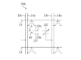
- FIG. 7 is an equivalent circuit diagram of the liquid crystal display device 50b according to the second embodiment.
- FIG. 1 is an equivalent circuit diagram of the liquid crystal display device 50a according to the first embodiment.
- FIG. 2 is a cross-sectional view of the TFT portion of the active matrix substrate 20a constituting the liquid crystal display device 50a.
- FIG. 8 is a cross-sectional view of the touch panel portion of the liquid crystal display device 50b.
- FIG. 9 is a plan view of the counter substrate 30b constituting the liquid crystal display device 50b.
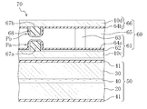
- FIG. 10 is a cross-sectional view of the liquid crystal display device 70 according to the third embodiment.
- FIG. 11 is a cross-sectional view of the first touch pin Pa and the second touch pin Pb constituting the liquid crystal display device according to the fourth embodiment.
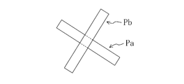
- FIG. 12 is a plan view of the first touch pin Pa and the second touch pin Pb constituting the liquid crystal display device according to the fifth embodiment.
- FIG. 13 is a cross-sectional view of the touch panel portion of the liquid crystal display device 150 of the comparative example.
- FIG. 1 is an equivalent circuit diagram of the liquid crystal display device 50a of the present embodiment.
- 2 is a cross-sectional view of the TFT portion of the active matrix substrate 20a constituting the liquid crystal display device 50a
- FIG. 3 is a cross-sectional view of the display portion of the liquid crystal display device 50a
- FIG. 4 is a liquid crystal display device. It is sectional drawing of the touchscreen part of 50a.
- FIG. 5 is a plan view of the counter substrate 30a constituting the liquid crystal display device 50a.
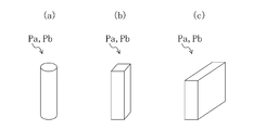
- FIGS. 6A to 6C are perspective views of the first touch pin Pa and the second touch pin Pb constituting the liquid crystal display device 50a.
- the liquid crystal display device 50a includes an active matrix substrate 20a and a counter substrate 30a that are arranged to face each other, a liquid crystal layer 40 provided between the active matrix substrate 20a and the counter substrate 30a, and an active matrix substrate 20a.
- a sealing material (not shown) provided in a frame shape is provided for adhering the matrix substrate 20a and the counter substrate 30a to each other and enclosing the liquid crystal layer 40 between the active matrix substrate 20a and the counter substrate 30a.
- the active matrix substrate 20a includes a plurality of gate lines 11 provided as first display lines so as to extend in parallel to each other on an insulating substrate 10a such as a glass substrate, and each gate line.
- a gate insulating film 12 provided so as to cover 11, and a plurality of source lines 14 a provided on the gate insulating film 12 as second display wirings so as to extend in parallel to each other in a direction orthogonal to each gate line 11,
- a plurality of TFTs 5 provided at each intersection of each gate line 11 and each source line 14a, and a first interlayer insulating film 15 and a second interlayer insulation provided in order so as to cover each source line 14a and each TFT 5
- a plurality of pixel electrodes 19 a provided in a matrix on the film 16 and the second interlayer insulating film 16 and connected to the respective TFTs 5 are provided between the pixel electrodes 19 a.
- a plurality of first touch panel wirings 19b provided so as to extend in parallel with each other so as to overlap each gate line 11a, and a part of each pixel electrode 19a and each first touch panel wiring 19b (each first touch pin described later) And an alignment film 9a provided so as to cover a portion other than Pa).
- an interlayer insulating film constituted by two layers including the first interlayer insulating film 15 and the second interlayer insulating film 16 is exemplified, but this interlayer insulating film is constituted by one layer. Also good.
- the TFT 5 includes a gate electrode 11 a in which each gate line 11 protrudes to the side, a gate insulating film 12 provided so as to cover the gate electrode 11 a, and a gate insulating film 12 on the gate insulating film 12.
- a semiconductor layer 13 provided in an island shape at a position overlapping the gate electrode 11a, and a source electrode (14a) and a drain electrode 14b provided so as to face each other on the semiconductor layer 13 are provided.
- the source electrode (14a) is a portion protruding to the side of each source line 14a. Further, as shown in FIG.
- the drain electrode 14b is formed on the transparent electrode 17a constituting the pixel electrode 19a through the contact hole 16c formed in the laminated film of the first interlayer insulating film 15 and the second interlayer insulating film 16. It is connected.
- the semiconductor layer 13 includes a lower intrinsic amorphous silicon layer 13a and an upper layer n + amorphous silicon layer 13b doped with phosphorus, and includes a source electrode (14a) and a drain electrode 14b. Intrinsic amorphous silicon layer 13a exposed from constitutes a channel region.
- the pixel electrode 19a includes a transparent electrode 17a provided on the second interlayer insulating film 16, and a reflective electrode 18a stacked on the transparent electrode 17a.
- the surface of the second interlayer insulating film 16 under the pixel electrode 19a (the reflective electrode 18a) is formed in an uneven shape as shown in FIG. 3, the surface of the second interlayer insulating film 16 is transparent.
- the surface of the reflective electrode 18a provided via the electrode 17a is also formed in an uneven shape.
- the first touch panel wiring 19b includes a transparent conductive layer 17b provided on the second interlayer insulating film 16 and a reflective conductive layer 18b stacked on the transparent conductive layer 17b. Yes.
- the second interlayer insulating film 16 below the first touch panel wiring 19b is formed in a convex shape in a region intersecting with a BM upper layer portion 25a described later.
- the wiring 19b has a first touch pin Pa formed in a column shape in the region.
- the reflective region R is defined by the reflective electrode 18a, and the transparent region 17a exposed from the reflective electrode 18a is transmissive region. T is specified.
- the counter substrate 30a is formed on, for example, an insulating substrate 10b such as a glass substrate, each gate line 11a (each first touch panel wiring 19b) on the active matrix substrate 20a, and A black matrix B provided in a frame shape and in a lattice shape in the frame so as to overlap each source line 14a, and a red layer 22a, a green layer 22b, and a blue layer provided in each opening of the black matrix B, respectively Color filter 22 including 22c, and each reflection region R of color filter 22, transparent layer 23a provided to compensate for an optical path difference in reflection region R and transmission region T, and each of the later-described components constituting black matrix B A plurality of BM lower layers 21a, a transparent region T of each color filter 22 and a transparent layer 23a (reflection region R) are provided so as to cover them.
- an insulating substrate 10b such as a glass substrate
- each gate line 11a each first touch panel wiring 19b
- a black matrix B provided in a frame shape and in a lat
- the black matrix B includes a BM lower layer portion 21a provided to overlap each gate line 11 (each first touch panel wiring 19b) on the active matrix substrate 20a, and an active matrix substrate.
- BM upper layer portion 25a provided as second touch panel wiring so as to overlap each source line 14a on 20a.
- the BM lower layer portion 21a is made of a resin, and is made of, for example, an organic insulating film in which a black pigment is dispersed.
- the BM upper layer portion 25a is made of, for example, a light-shielding metal film such as a chromium film, and has conductivity. Further, as shown in FIG. 4, the BM upper layer portion 25a is provided with a convex resin layer 23b below the first touch panel wiring 19b, so that the BM upper layer portion 25a is formed in a columnar shape. It has 2 touch pins Pb.
- the first touch pin Pa and the second touch pin Pb are, for example, a cylindrical shape as shown in FIG. 6A, a rectangular parallelepiped shape whose upper surface is square as shown in FIG. 6B, and FIG. As shown in c), the upper surface is formed in a rectangular parallelepiped shape or the like.
- the common electrodes 24a are provided in stripes so as to extend in parallel with each other between the BM upper layer portions 25a.
- the liquid crystal layer 40 is made of a nematic liquid crystal material having electro-optical characteristics.
- the transflective liquid crystal display device 50a configured as described above reflects light incident from the counter substrate 30a side in the reflective region R by the reflective electrode 18a and from the backlight incident from the active matrix substrate 20a side in the transmissive region T. It is configured to transmit light.
- the liquid crystal display device 50a when displaying an image, in each pixel, when the gate signal is sent from the gate line 11 to the gate electrode 11a and the TFT 5 is turned on, the source signal is sent from the source line 14a to the source. It is sent to the electrode (14a), and a predetermined charge is written into the pixel electrode 19a composed of the transparent electrode 17a and the reflective electrode 18a via the semiconductor layer 13 and the drain electrode 14b.
- a potential difference is generated between each pixel electrode 19a of the active matrix substrate 20a and each common electrode 24a of the counter substrate 30a, and a predetermined voltage is applied to the liquid crystal layer 40.
- the liquid crystal display device 50a by changing the alignment state of the liquid crystal layer 40 according to the magnitude of the voltage applied to the liquid crystal layer 40, the light transmittance of the liquid crystal layer 40 is adjusted and an image is displayed.
- the liquid crystal display device 50a when the surface of the active matrix substrate 20a or the counter substrate 30a is pressed, the first touch pins Pa of the first touch panel wiring 19b and the BM upper layer portion 25a (second touch panel wiring) first. When the two touch pins Pb come into contact with each other and are conducted, the pressed touch position is detected.
- the manufacturing method of this embodiment includes an active matrix substrate manufacturing process, a counter substrate manufacturing process, and a substrate bonding process.
- a titanium film, an aluminum film, a titanium film, and the like are sequentially formed on the entire substrate of the insulating substrate 10a such as a glass substrate by a sputtering method, and then patterned by photolithography to form the gate line 11 and the gate electrode.
- 11a is formed to a thickness of about 4000 mm.
- a silicon nitride film or the like is formed on the entire substrate on which the gate line 11 and the gate electrode 11a are formed by a plasma CVD (Chemical Vapor Deposition) method, and the gate insulating film 12 is formed to a thickness of about 4000 mm. To do.
- a plasma CVD Chemical Vapor Deposition
- an intrinsic amorphous silicon film (thickness of about 2000 mm) and phosphorus-doped n + amorphous silicon film (thickness of about 500 mm) are formed on the entire substrate on which the gate insulating film 12 is formed by plasma CVD. Films are continuously formed, and then patterned into island shapes on the gate electrode (11a) by photolithography to form a semiconductor formation layer in which an intrinsic amorphous silicon layer and an n + amorphous silicon layer are stacked.
- an aluminum film and a titanium film are sequentially formed on the entire substrate on which the semiconductor formation layer has been formed by sputtering, and then patterned by photolithography to form a source line 14a and a source electrode (14a).
- the drain electrode 14b is formed to a thickness of about 2000 mm.
- the n + amorphous silicon layer of the semiconductor formation layer is etched by using the source electrode (14a) and the drain electrode 14b as a mask, thereby patterning the channel region to form the semiconductor layer 13 and the TFT 5 including the same. .
- a silicon nitride film is formed on the entire substrate on which the TFT 5 is formed by a plasma CVD method, and the first interlayer insulating film 15 is formed to a thickness of about 4000 mm.
- a positive photosensitive resin is applied to a thickness of about 3 ⁇ m by spin coating on the entire substrate on which the first interlayer insulating film 15 is formed, and the applied photosensitive resin is applied to a plurality of circles.
- the first photomask formed with the light-shielding portions spaced apart from each other at random exposure is performed uniformly and with relatively low illuminance, and subsequently, at a position corresponding to the contact hole 16c on the drain electrode 14b. Development is carried out after exposure with uniform and relatively high illuminance through a second photomask in which openings are respectively formed.
- the photosensitive resin in the exposed portion with the high illuminance is completely removed, and the photosensitive resin in the exposed portion with the low illuminance remains about 40% of the coating thickness, and the photosensitive resin in the unexposed portion. Will leave about 80% of the coating thickness.
- the photosensitive resin in the exposed portion with the high illuminance is completely removed, and the photosensitive resin in the exposed portion with the low illuminance remains about 40% of the coating thickness, and the photosensitive resin in the unexposed portion. Will leave about 80% of the coating thickness.
- a second interlayer insulating film 16 having a convex surface is formed. Thereafter, the first interlayer insulating film 15 exposed from the second interlayer insulating film 16 is etched to form contact holes 16c.
- a transparent conductive film made of an ITO (Indium Tin Oxide) film or the like is formed on the entire substrate on the second interlayer insulating film 16 by a sputtering method, and then patterned by photolithography to form the transparent electrode 17a and the transparent electrode.
- the conductive layer 17b is formed to a thickness of about 1000 mm.
- a molybdenum film (thickness of about 750 mm) and an aluminum film (thickness of about 1000 mm) are sequentially formed on the entire substrate on which the transparent electrode 17a and the transparent conductive layer 17b are formed, and then patterned by photolithography. Then, the reflective electrode 18a and the reflective conductive layer 18b are formed, and the pixel electrode 19a including the transparent electrode 17a and the reflective electrode 18a, and the first touch panel wiring 19b including the transparent conductive layer 17b and the reflective conductive layer 18b are formed.
- a polyimide resin is applied to the entire substrate on which the pixel electrode 19a and the first touch panel wiring 19b are formed by a printing method, and then a rubbing process is performed to form an alignment film 9a having a thickness of about 1000 mm.
- the active matrix substrate 20a can be manufactured.
- ⁇ Opposite substrate manufacturing process First, an acrylic photosensitive resin in which black pigments such as carbon fine particles are dispersed is applied to the entire substrate of the insulating substrate 10b such as a glass substrate by a spin coating method, and the applied photosensitive resin is photo-coated. After exposure through a mask, patterning is performed by developing to form the BM lower layer portion 21a with a thickness of about 2.0 ⁇ m.
- the transparent layer 23b is formed to a thickness of about 2.0 ⁇ m.
- a chromium film is formed on the entire substrate on which the resin layer 23b is formed by sputtering, and then patterned by photolithography to form the BM upper layer portion 25a with a thickness of about 2000 mm.
- an acrylic photosensitive resin colored in red, green, or blue is applied on the substrate on which the BM upper layer portion 25a is formed, and the applied photosensitive resin is exposed through a photomask.
- patterning is performed by developing to form a colored layer (for example, red layer 22a) of a selected color with a thickness of about 2.0 ⁇ m.
- the same process is repeated for the other two colors to form the other two colored layers (for example, the green layer 22b and the blue layer 22c) with a thickness of about 2.0 ⁇ m, and the red layer 22a and the green layer.
- the color filter 22 including the layer 22b and the blue layer 22c is formed.
- an acrylic photosensitive resin is applied onto the substrate on which the color filter 22 is formed by spin coating, and the applied photosensitive resin is exposed through a photomask and then developed.
- the transparent layer 23a is formed to a thickness of about 2 ⁇ m.
- an ITO film is formed on the entire substrate on which the transparent layer 23a is formed by sputtering, and then patterned by photolithography to form the common electrode 24a with a thickness of about 1500 mm.
- an acrylic photosensitive resin is applied to the entire substrate on which the common electrode 24a is formed by a spin coating method, and the applied photosensitive resin is exposed through a photomask and then developed.
- the photo spacer 26 is formed to a thickness of about 4 ⁇ m.
- a polyimide resin is applied to the entire substrate on which the photo spacers 26 are formed by a printing method, and then a rubbing process is performed to form an alignment film 9b with a thickness of about 1000 mm.
- the counter substrate 30a can be manufactured.
- a seal material made of ultraviolet curing and thermosetting resin is drawn in a frame shape on the counter substrate 30a manufactured in the counter substrate manufacturing step.
- a liquid crystal material is dropped onto a region inside the sealing material in the counter substrate 30a on which the sealing material is drawn.
- the bonded body is released to atmospheric pressure. By doing, the surface and the back surface of the bonded body are pressurized.
- the sealing material is cured by heating the bonded body.
- the liquid crystal display device 50a can be manufactured as described above.
- each BM upper layer functioning as each first touch panel wiring 19b on the active matrix substrate 20a and each second touch panel wiring on the counter substrate 30a. 25a intersects via the alignment film 9a / liquid crystal layer 40 / alignment film 9b, and when the surface of the active matrix substrate 20a or the counter substrate 30a is pressed, each first touch panel wiring 19b and each BM upper layer portion 25a.
- the type resistive film type touch panel is built in the liquid crystal display device.
- each first touch pin Pa and each second touch pin Pb are brought into contact with each other so that each first touch panel wiring 19b and each BM upper layer portion 25a are electrically connected to each other, so that the touch pins are provided only on one side of the active matrix substrate and the counter substrate.
- the counter substrate 130 has a second touch panel wiring 125 on the insulating substrate 110b.
- the first touch panel wiring 119 on the insulating substrate 110a does not have a touch pin.
- the surface portion of the active matrix substrate 120 with which the top of the substrate abuts There than covered if easily) in the alignment film 109, alignment films 9a and 9b may not become a resistance component between the first wiring 19b and the BM layer portion 25a for a touch panel. Therefore, in the matrix-type resistive touch panel built in the liquid crystal display device, conduction at the top of the touch pin can be ensured.
- the photo spacer 26 since the photo spacer 26 is sandwiched between the active matrix substrate 20a and the counter substrate 30a, the surface of the active matrix substrate 20a or the counter substrate 30a is pressed. If not, the insulating property between each first touch panel wiring 19b on the active matrix substrate 20a and each BM upper layer portion 25a on the counter substrate 30a can be held by the photo spacer 26.
- FIG. 7 is an equivalent circuit diagram of the liquid crystal display device 50b of the present embodiment.
- 8 is a cross-sectional view of the touch panel portion of the liquid crystal display device 50b
- FIG. 9 is a plan view of the counter substrate 30b constituting the liquid crystal display device 50b.
- the same portions as those in FIGS. 1 to 6 are denoted by the same reference numerals, and detailed description thereof is omitted.
- the first display wiring is a gate line and the second display wiring is a source line.
- the first display wiring is used. Is a source line, and the second display wiring is a gate line.
- the liquid crystal display device 50b includes an active matrix substrate 20b and a counter substrate 30b that are disposed to face each other, a liquid crystal layer 40 provided between the active matrix substrate 20b and the counter substrate 30b, and an active matrix substrate 20b.
- a sealing material (not shown) provided in a frame shape is provided for adhering the matrix substrate 20b and the counter substrate 30b to each other and enclosing the liquid crystal layer 40 between the active matrix substrate 20b and the counter substrate 30b.
- the active matrix substrate 20b includes a plurality of gate lines 11 provided as second display wirings so as to extend in parallel to each other on an insulating substrate 10a such as a glass substrate, and each gate line.
- a gate insulating film 12 provided so as to cover 11, and a plurality of source lines 14 a provided on the gate insulating film 12 as first display wirings so as to extend in parallel to each other in a direction orthogonal to each gate line 11,
- a plurality of TFTs 5 provided at each intersection of each gate line 11 and each source line 14a, and a first interlayer insulating film 15 and a second interlayer insulation provided in order so as to cover each source line 14a and each TFT 5 Provided between each pixel electrode 19a and a plurality of pixel electrodes 19a provided in a matrix on the film 16 and the second interlayer insulating film 16 and connected to each TFT 5.
- first touch panel wirings 19c provided so as to extend in parallel with each other so as to overlap with each source line 14a, a part of each pixel electrode 19a and each first touch panel wiring 19c (each first touch panel described later).
- an alignment film 9a provided so as to cover a portion other than the touch pin Pa).
- the first touch panel wiring 19c is formed on the second interlayer insulating film 16 simultaneously with the transparent electrode 17a and on the transparent conductive layer 17cb simultaneously with the reflective electrode 18a. And the reflective conductive layer 18cb.
- the second interlayer insulating film 16 below the first touch panel wiring 19 c is formed in a convex shape in a region intersecting with a BM upper layer portion 25 a described later.
- the wiring 19c has a first touch pin Pa formed in a column shape in the region.
- the counter substrate 30b is formed on, for example, an insulating substrate 10b such as a glass substrate, each gate line 11 and each source line 14a (each first touch panel wiring 19cb on the active matrix substrate 20b).
- a black matrix B provided in a frame shape and in a lattice shape in the frame, and a red layer 22a, a green layer 22b, and a blue layer 22c provided in each opening of the black matrix B, respectively.
- each reflective area R of the color filter 22 and the color filter 22 a transparent layer 23 a provided to compensate for an optical path difference in the reflective area R and the transmissive area T, and each BM lower layer portion described later constituting the black matrix B 21b, a plurality of common filters provided so as to cover the transmission region T and the transparent layer 23a (reflection region R) of each color filter 22.
- an alignment film 9b provided so as to cover the respective photo spacers 26.
- the black matrix B includes a BM lower layer portion 21b provided to overlap each source line 14a (each first touch panel wiring 19c) on the active matrix substrate 20b, and an active matrix substrate.
- BM upper layer portion 25b provided as a second touch panel wiring so as to overlap each gate line 11 on 20b.
- the BM lower layer portion 21b is made of a resin and is made of, for example, an organic insulating film in which a black pigment is dispersed.
- the BM upper layer portion 25b is made of, for example, a light-shielding metal film such as a chromium film, and has conductivity.
- the BM upper layer portion 25b is formed in a columnar shape because the convex resin layer 23b is provided in the lower layer in the region intersecting with each first touch panel wiring 19c.
- a second touch pin Pb is provided.
- the common electrodes 24b are provided in stripes so as to extend in parallel with each other between the BM upper layer portions 25b.
- the transflective liquid crystal display device 50b having the above configuration reflects light incident from the counter substrate 30b side in the reflective region R by the reflective electrode 18a and from the backlight incident from the active matrix substrate 20b side in the transmissive region T. It is configured to transmit light.
- the liquid crystal display device 50b when an image is displayed, in each pixel, when the gate signal is sent from the gate line 11 to the gate electrode 11a and the TFT 5 is turned on, the source signal is sent from the source line 14a to the source. It is sent to the electrode (14a), and a predetermined charge is written into the pixel electrode 19a composed of the transparent electrode 17a and the reflective electrode 18a via the semiconductor layer 13 and the drain electrode 14b.
- a potential difference is generated between each pixel electrode 19a of the active matrix substrate 20b and each common electrode 24b of the counter substrate 30b, and a predetermined voltage is applied to the liquid crystal layer 40.
- an image is displayed by adjusting the light transmittance of the liquid crystal layer 40 by changing the alignment state of the liquid crystal layer 40 according to the magnitude of the voltage applied to the liquid crystal layer 40.
- the liquid crystal display device 50b when the surface of the active matrix substrate 20b or the counter substrate 30b is pressed, the first touch pins Pa of the first touch panel wiring 19c and the first of the BM upper layer portion 25b (second touch panel wiring). When the two touch pins Pb come into contact with each other and are conducted, the pressed touch position is detected.
- liquid crystal display device 50b of this embodiment can be manufactured by changing the pattern shape of the constituent thin film in the active matrix manufacturing process and the counter substrate manufacturing process described in the first embodiment. Description is omitted.
- the alignment films 9a and 9b have the resistance component between the first touch panel wiring 19c and the BM upper layer portion 25b. Therefore, in the matrix type resistive touch panel built in the liquid crystal display device, conduction at the top of the touch pin can be ensured.
- FIG. 10 is a cross-sectional view of the liquid crystal display device 70 of the present embodiment.
- a matrix type resistive film type touch panel is built-in.
- the matrix type resistive film type touch panel 60 of the liquid crystal display panel 50 is used. It is mounted on the front.
- the liquid crystal display device 70 includes a liquid crystal display panel 50 having a polarizing plate 41 attached to the upper surface and the lower surface, and an upper surface (front surface) of the liquid crystal display panel 50 attached to the upper surface (front surface) via a double-sided adhesive tape. And a matrix type resistive film type touch panel 60 attached thereto.
- the liquid crystal display panel 50 includes, for example, an active matrix substrate 20 and a counter substrate 30 that are arranged to face each other, and a liquid crystal layer 40 provided between the active matrix substrate 20 and the counter substrate 30.
- the active matrix substrate 20 and the counter substrate 30 are bonded to each other, and a sealing material (not shown) provided in a frame shape is provided between the active matrix substrate 20 and the counter substrate 30 to enclose the liquid crystal layer 40. .
- the active matrix substrate 20 includes, for example, a plurality of gate lines (not shown) provided so as to extend in parallel to each other on an insulating substrate (not shown) such as a glass substrate, and a gate provided so as to cover each gate line.
- a plurality of pixel electrodes (not shown) respectively connected to the TFT, and an alignment film (not shown) provided so as to cover each pixel electrode are provided.
- the counter substrate 30 is provided in a frame shape and in a lattice shape in the frame so as to overlap each gate line and each source line on the active matrix substrate 20 on an insulating substrate (not shown) such as a glass substrate, for example.
- an insulating substrate such as a glass substrate, for example.
- a black matrix not shown
- a color filter not shown
- a common electrode not shown
- a plurality of photo spacers (not shown) provided in a columnar shape on the electrode, and an alignment film (not shown) provided so as to cover the common electrode and each photo spacer.
- the touch panel 60 includes a first substrate 61 and a second substrate 66 that are arranged to face each other, and an air layer 65 provided as an intermediate layer between the first substrate 61 and the second substrate 66. And.
- the first substrate 61 includes, for example, a plurality of first touch panel wirings 62 formed of an ITO film or the like so as to extend in parallel to each other on an insulating substrate 10c such as a glass substrate, and the insulating substrate 10c.
- a plurality of spacers 63 formed in a columnar shape on an acrylic resin or the like, a part of each first touch panel wiring 62 (a part other than each first touch pin Pa described later), and each spacer 63 are provided.
- a protective film 64a made of resin.
- the first touch panel wiring 62 is formed in a columnar shape because a convex resin layer 67a is provided in a lower layer in a region intersecting each second touch panel wiring 68 described later.
- the first touch pin Pa is provided.
- the second substrate 66 includes, for example, a plurality of second touch panel wires 68 formed of an ITO film or the like so as to extend in parallel with each other on an insulating substrate 10d such as a glass substrate. And a resin protective film 64b provided so as to cover a part of the touch panel wiring 68 (a part other than each second touch pin Pb described later).
- the second touch panel wiring 68 is provided with a convex resin layer 67b in a lower layer in a region intersecting with each first touch panel wiring 62. It has 2 touch pins Pb.
- the touch panel 60 configured as described above, when the surface of the second substrate 66 is pressed, the first touch pin Pa of the first touch panel wiring 62 and the second touch pin Pb of the second touch panel wiring 68 are brought into contact with each other to be conductive. By doing so, the pressed touch position is detected.
- each first touch panel wiring 62 on the first substrate 61 and each second touch panel wiring 68 on the second substrate 66 are: When the surface of the second substrate 66 is pressed by crossing through the protective film 64a / air layer 65 / protective film 64b, the first touch panel wiring 62 and the second touch panel wiring 68 are respectively connected to the first touch panel wiring 68. Since each of the first touch pins Pa provided on the touch panel wiring 62 and each second touch pin Pb provided on each second touch panel wiring 68 are configured to be electrically connected to each other, a matrix type resistor is provided. A membrane-type touch panel is specifically configured.
- the top portions of the first touch pins Pa and the second touch pins Pb provided in a columnar shape protrude from the surfaces of the first substrate 61 and the second substrate 66, and thus the first substrate 61 and the second substrate 62 are provided. It is harder to be covered with the protective films 64a and 64b than in the flat part.
- the first touch panel wiring 62 and the second touch panel wiring 68 are electrically connected to each other by the contact between the first touch pins Pa and the second touch pins Pb, only one side of the first substrate and the second substrate is provided. Touch pins are provided (for example, the first touch pin of the first substrate is present and the second touch pin of the second substrate is not present, and the top portion of the first touch pin is applied when pressed.
- the protective films 64a and 64b do not become a resistance component between the first touch panel wiring 62 and the second touch panel wiring 68 than in the case where the surface portion of the second substrate that is in contact is easily covered with the protective film. Therefore, in the matrix type resistive film type touch panel, conduction at the top of the touch pin can be ensured.
- an active matrix driving liquid crystal display panel is exemplified as the display panel.
- the present invention is a passive matrix driving liquid crystal display panel, an active matrix driving or passive matrix driving organic EL (electroluminescence).
- the present invention can also be applied to other display panels such as a display panel.
- FIG. 11 is a cross-sectional view of the first touch pin Pa and the second touch pin Pb constituting the liquid crystal display device of the present embodiment.
- first touch pin Pa and the second touch pin Pb formed in a columnar shape are illustrated, but in this embodiment, the top portion of the first touch pin Pa or the second touch pin Pb is formed in a concave shape.
- the top portion of the first touch pin Pa constituting the liquid crystal display device of the present embodiment is formed in a concave shape.
- the second touch pin Pb is formed in a columnar shape so that the top portion thereof fits into the concave portion of the first touch pin Pa.
- the alignment film does not become a resistance component between the first touch panel wiring and the second touch panel wiring, as in the first and second embodiments.
- conduction at the top of the touch pin can be ensured.
- the convex portion at the edge of the first touch pin Pa formed in the concave shape serves as a fulcrum.
- the first touch pin Pa and the second touch pin Pb in the touch panel built in the liquid crystal display device are exemplified, but the present invention can also be applied to the first touch pin and the second touch pin in the touch panel alone. it can.
- FIG. 12 is a plan view of the first touch pin Pa and the second touch pin Pb constituting the liquid crystal display device of the present embodiment.
- the first touch pin Pa and the second touch pin Pb configured such that the top portions overlap each other are illustrated.
- the first touch pin Pa and the second touch pin Pb intersect each other. It is configured as follows.
- the first touch pin Pa constituting the liquid crystal display device of the present embodiment is formed in a linear shape so as to extend along the gate line 11, for example, as shown in FIG.
- the second touch pin Pb is formed in a linear shape so as to extend along the source line 14a, for example, and is provided so as to be orthogonal to the first touch pin Pa.
- the alignment film does not become a resistance component between the first touch panel wiring and the second touch panel wiring, as in the first, second, and fourth embodiments.
- conduction at the top of the touch pin can be ensured.
- each first touch pin Pa and each second touch pin Pb are formed in a linear shape so as to intersect with each other, so that the active matrix substrate and the counter substrate are bonded together. Even if the position shift occurs, the first touch pins Pa and the second touch pins Pb can be brought into contact with each other.
- the first touch pin Pa and the second touch pin Pb in the touch panel built in the liquid crystal display device are exemplified, but the present invention can also be applied to the first touch pin and the second touch pin in the touch panel alone. it can.
- the configuration in which one touch panel wiring is provided for each display wiring of the gate line and the source line is illustrated.
- the present invention is provided for each of a plurality of adjacent display wirings.
- a configuration in which one touch panel wiring is provided may be used, that is, the touch panel wiring may be thinned to reduce the number of touch panel wirings.
- the configuration in which the first touch panel wiring is formed at the same time as the pixel electrode 19a is illustrated.
- the present invention has a configuration in which the first touch panel wiring is formed at the same time as the gate line or the source line. There may be.
- a transflective liquid crystal display device is exemplified, but the present invention can also be applied to a transmissive or reflective liquid crystal display device.
- a single-touch touch panel is exemplified, but the present invention can also be applied to a multi-touch touch panel.
- the liquid crystal display device includes TN (Twisted Nematic), VA (Vertical Alignment), MVA (Multi-domain Vertical Alignment), ASV (Advanced Super View), and IPS (In-Plane-Switching). It may be a simple method.
- the present invention is useful for a car navigation system, a PDA (Personal Digital Assistant), etc., because the device itself can be made thin and light in a liquid crystal display device equipped with a resistive touch panel. It is useful for mobile devices such as mobile phones, notebook computers, portable game machines, and digital cameras.
- Second touch pins 9a, 9b Alignment film 11 Gate line (first display wiring or second display wiring) 14a Source line (second display wiring or first display wiring) 19b, 19c, 62 First touch panel wiring 20, 20a, 20b Active matrix substrates 25a, 25b BM upper layer (second touch panel wiring) 26 Photospacer 30, 30a, 30b Counter substrate 40 Liquid crystal layer 50 Liquid crystal display panel 50a, 50b, 70 Liquid crystal display device 60 Touch panel 61 First substrate 66 Second substrate 64a, 64b Protective film 65 Air layer (intermediate layer) 68 Wiring for second touch panel
Landscapes
- Engineering & Computer Science (AREA)
- Physics & Mathematics (AREA)
- General Engineering & Computer Science (AREA)
- Theoretical Computer Science (AREA)
- General Physics & Mathematics (AREA)
- Nonlinear Science (AREA)
- Human Computer Interaction (AREA)
- Mathematical Physics (AREA)
- Chemical & Material Sciences (AREA)
- Crystallography & Structural Chemistry (AREA)
- Optics & Photonics (AREA)
- Liquid Crystal (AREA)
Abstract
互いに平行に延びるように複数の第1タッチパネル用配線(19b)が設けられたアクティブマトリクス基板(20a)と、アクティブマトリクス基板(20a)に対向して配置され、各第1タッチパネル用配線(19b)に交差する方向に互いに平行に延びるように複数の第2タッチパネル用配線(25a)が設けられた対向基板(30a)と、アクティブマトリクス基板(20a)及び対向基板(30a)の間に配向膜(9a)及び(9b)を介して設けられた液晶層(40)とを備え、各第1タッチパネル用配線(19b)は、各第2タッチパネル用配線(25a)に交差する領域に、柱状に設けられた複数の第1タッチピン(Pa)を有し、各第2タッチパネル用配線(25a)は、各第1タッチパネル用配線(19b)に交差する領域に、柱状に設けられた複数の第2タッチピン(Pb)を有している。
Description
本発明は、タッチパネル及びそれを備えた表示装置並びに液晶表示装置に関するものである。
タッチパネルは、指やペンなどでタッチ(押圧)することによって、コンピュータなどの情報処理装置に対話形式で情報を入力する装置である。
また、タッチパネルは、その動作原理によって、抵抗膜方式、静電容量結合方式、赤外線方式、超音波方式及び電磁誘導結合方式などに分類されている。ここで、抵抗膜方式及び静電容量結合方式のタッチパネルは、低コストで表示装置などに搭載可能であるので、近年よく利用されている。
上記抵抗膜方式のタッチパネルは、例えば、互いに対向して配置された一対の基板と、一対の基板の内側に抵抗膜としてそれぞれ設けられた一対の透明導電膜と、一対の基板の間に挟持されて一対の透明導電膜の間に空気層を形成する絶縁性を有するスペーサと、タッチされた位置を検出するための位置検出回路とを備え、例えば、液晶表示パネルの表示画面の前面に搭載して使用される。
このような構成の抵抗膜方式のタッチパネルでは、その表面がタッチされることにより、一対の透明導電膜同士が接触(短絡)して、一対の透明導電膜の間に電流が流れることになり、位置検出回路が一対の透明導電膜の間に電流が流れたときの電圧の変化に基づいてタッチされた位置を検出することになる。
ところで、液晶表示パネルは、例えば、互いに対向して配置されたアクティブマトリクス基板及び対向基板と、アクティブマトリクス基板及び対向基板の間に設けられた液晶層とを備えている。そのため、上記抵抗膜方式のタッチパネルが液晶表示パネルの前面に搭載された液晶表示装置では、構成基板が、タッチパネルを構成する一対の基板、アクティブマトリクス基板及び対向基板の4枚からなり、装置全体の厚さが増大してしまう。
そこで、例えば、特許文献1には、液晶表示パネルのカラーフィルター基板をタッチセンサの固定電極板として利用することにより、タッチセンサパネルを構成していた固定電極板が廃止されたタッチセンサ式液晶表示装置が開示されている。そして、これによれば、タッチセンサ式液晶表示装置の厚さ及び重量を低減することができ、光学特性の劣化を防止する効果も有する、と記載されている。
しかしながら、特許文献1に記載された発明では、タッチセンサ式液晶表示装置を構成する構成基板が3枚であり、改善の余地があるので、例えば、マトリクス型の抵抗膜方式のタッチパネルが内蔵された液晶表示装置(液晶表示パネル)が、近年、提案されている。
このマトリクス型の抵抗膜方式のタッチパネルが内蔵された液晶表示装置は、例えば、アクティブマトリクス基板の液晶層側の表面に互いに平行に延びるように一方の抵抗膜として設けられた複数の第1タッチパネル用配線と、対向基板の液晶層側の表面に各第1タッチパネル用配線と直交する方向に互いに平行に延びるように他方の対向膜として設けられた複数の第2タッチパネル配線とを備え、アクティブマトリクス基板又は対向基板の表面が押圧されたときに、その押圧された位置でその位置に対応する第1タッチパネル用配線及び第2タッチパネル配線が互いに接触して導通するように構成されている。ここで、各第1タッチパネル用配線又は各第2タッチパネル配線は、その交差部に柱状に設けられたタッチピンを有しており、このタッチピンを介して、押圧された位置の第1タッチパネル用配線及び第2タッチパネル配線が互いに導通することになる。
しかしながら、液晶表示パネルでは、アクティブマトリクス基板及び対向基板の液晶層側の各表面に液晶層の液晶分子を配向させるための配向膜を設ける必要があるので、配向膜が第1タッチパネル用配線と第2タッチパネル配線との間の抵抗成分となり、タッチパネルの機能に支障を来たすおそれがある。
また、上述した配向膜によるタッチパネルの機能への支障の問題に限らず、マトリクス型の抵抗膜方式のタッチパネル単体において、タッチピンの側面だけを絶縁膜で覆って、タッチピンの頂部を絶縁膜から露出させることは、例えば、導電性異物などに起因する第1タッチパネル用配線と第2タッチパネル配線との間の不要な短絡を抑制することができるので、有効である。
本発明は、かかる点に鑑みてなされたものであり、その目的とするところは、マトリクス型の抵抗膜方式のタッチパネルにおいて、タッチピンの頂部における導通を確実にすることにある。
上記目的を達成するために、本発明は、第1タッチパネル用配線及び第2タッチパネル用配線が第1タッチピン及び第2タッチピンをそれぞれ有し、第1タッチピン及び第2タッチピンが互いに接触することにより、第1タッチパネル用配線及び第2タッチパネル用配線が互いに導通するようにしたものである。
具体的に本発明に係る液晶表示装置は、互いに平行に延びるように複数の第1タッチパネル用配線が設けられたアクティブマトリクス基板と、上記アクティブマトリクス基板に対向して配置され、上記各第1タッチパネル用配線に交差する方向に互いに平行に延びるように複数の第2タッチパネル用配線が設けられた対向基板と、上記アクティブマトリクス基板及び対向基板の間にそれぞれ配向膜を介して設けられた液晶層とを備えた液晶表示装置であって、上記各第1タッチパネル用配線は、上記各第2タッチパネル用配線に交差する領域に、柱状に設けられた複数の第1タッチピンを有し、上記各第2タッチパネル用配線は、上記各第1タッチパネル用配線に交差する領域に、柱状に設けられた複数の第2タッチピンを有し、上記アクティブマトリクス基板又は対向基板の表面が押圧されたときに、上記各第1タッチピン及び各第2タッチピンが互いに接触することにより、上記各第1タッチパネル用配線及び各第2タッチパネル用配線が互いに導通するように構成されていることを特徴とする。
上記の構成によれば、アクティブマトリクス基板上の各第1タッチパネル用配線と、対向基板上の各第2タッチパネル用配線とは、(配向膜/)液晶層(/配向膜)を介して交差し、アクティブマトリクス基板又は対向基板の表面が押圧されたときに、各第1タッチパネル用配線及び各第2タッチパネル用配線が、各第1タッチパネル用配線に設けられた各第1タッチピン、及び各第2タッチパネル用配線に設けられた各第2タッチピンを介して、互いに導通するように構成されているので、マトリクス型の抵抗膜方式のタッチパネルが液晶表示装置に内蔵されることになる。ここで、柱状に設けられた各第1タッチピン及び各第2タッチピン(の頂部)は、アクティブマトリクス基板及び対向基板の各表面において突出しているので、アクティブマトリクス基板及び対向基板における平坦な部分よりも配向膜で覆われ難い。しかも、各第1タッチピンと各第2タッチピンとの接触により、各第1タッチパネル用配線及び各第2タッチパネル用配線が互いに導通するので、アクティブマトリクス基板及び対向基板の一方側のみにタッチピンが設けられている場合(例えば、アクティブマトリクス基板上の第1タッチピンが存在して、対向基板上の第2タッチピンが存在しない場合であって、押圧されたときに第1タッチピンの頂部が当接する対向基板の表面部分が配向膜で覆われ易い場合)よりも、配向膜が第1タッチパネル用配線と第2タッチパネル用配線との間の抵抗成分とならなくなる。したがって、液晶表示装置に内蔵されたマトリクス型の抵抗膜方式のタッチパネルにおいて、タッチピンの頂部における導通を確実にすることが可能になる。
上記各第1タッチピン又は各第2タッチピンの頂部は、凹状に形成されていてもよい。
上記の構成によれば、各第1タッチピン又は各第2タッチピンの頂部が凹状に形成されているので、頂部が凹状に形成されたタッチピンの縁の凸部がてこの支点となることにより、各第1タッチパネル用配線と各第2タッチパネル用配線との貼り付きによる常時短絡を抑制することが可能になる。さらに、頂部における接触面積が増えるので、タッチピンの頂部における導通をより確実にすることが可能になる。
上記各第1タッチピン及び各第2タッチピンは、互いに交差するように線状に形成されていてもよい。
上記の構成によれば、各第1タッチピン及び各第2タッチピンが互いに交差するように線状に形成されているので、アクティブマトリクス基板と対向基板とを貼り合わせる際に位置ずれが発生しても、各第1タッチピンと各第2タッチピンとを互いに接触させることが可能になる。
上記アクティブマトリクス基板は、互いに平行に延びるように設けられた複数の第1表示用配線と、該各第1表示用配線に交差する方向に互いに平行に延びるように設けられた複数の第2表示用配線とを有し、上記各第1タッチパネル用配線は、上記各第1表示用配線に沿って設けられ、上記各第2タッチパネル用配線は、上記各第2表示用配線に沿って設けられていてもよい。
上記の構成によれば、アクティブマトリクス基板が互いに平行に延びる複数の第1表示用配線と、各第1表示用配線に交差する方向に互いに平行に延びる複数の第2表示用配線とを有し、各第1タッチパネル用配線が各第1表示用配線に沿って設けられ、各第2タッチパネル用配線が各第2表示用配線に沿って設けられているので、互いに平行に延びる複数のゲート線と、各ゲート線に交差する方向に互いに平行に延びる複数のソース線と、各ゲート線又は各ソース線に沿って設けられた各第1タッチパネル用配線とを備えたアクティブマトリクス基板、及び各第2タッチパネル用配線を備えた対向基板が具体的に構成される。
上記アクティブマトリクス基板又は対向基板には、上記液晶層の厚さを規定するための柱状のフォトスペーサが設けられていてもよい。
上記の構成によれば、アクティブマトリクス基板及び対向基板の間に、フォトスペーサが挟持されることになるので、アクティブマトリクス基板又は対向基板の表面が押圧されていないときには、アクティブマトリクス基板上の各第1タッチパネル用配線と、対向基板上の各第2タッチパネル用配線との絶縁性がフォトスペーサにより保持されることになる。
また、本発明に係るタッチパネルは、互いに平行に延びるように複数の第1タッチパネル用配線が設けられた第1基板と、上記第1基板に対向して配置され、上記各第1タッチパネル用配線と交差する方向に互いに平行に延びるように複数の第2タッチパネル用配線が設けられた第2基板と、上記第1基板及び第2基板の間にそれぞれ保護膜を介して設けられた中間層とを備えたタッチパネルであって、上記各第1タッチパネル用配線は、上記各第2タッチパネル用配線に交差する領域に、柱状に設けられた複数の第1タッチピンを有し、上記各第2タッチパネル用配線は、上記各第1タッチパネル用配線に交差する領域に、柱状に設けられた複数の第2タッチピンを有し、上記第1基板又は第2基板の表面が押圧されたときに、上記各第1タッチピン及び各第2タッチピンが互いに接触することにより、上記各第1タッチパネル用配線及び各第2タッチパネル用配線が互いに導通するように構成されていることを特徴とする。
上記の構成によれば、第1基板上の各第1タッチパネル用配線と、第2基板上の各第2タッチパネル用配線とは、(保護膜/)中間層(/保護膜)を介して交差し、第1基板又は第2基板の表面が押圧されたときに、各第1タッチパネル用配線及び各第2タッチパネル用配線が、各第1タッチパネル用配線に設けられた各第1タッチピン、及び各第2タッチパネル用配線に設けられた各第2タッチピンを介して、互いに導通するように構成されているので、マトリクス型の抵抗膜方式のタッチパネルが具体的に構成されることになる。ここで、柱状に設けられた各第1タッチピン及び各第2タッチピン(の頂部)は、第1基板及び第2基板の各表面において突出しているので、第1基板及び第2基板における平坦な部分よりも保護膜で覆われ難い。しかも、各第1タッチピンと各第2タッチピンとの接触により、各第1タッチパネル用配線及び各第2タッチパネル用配線が互いに導通するので、第1基板及び第2基板の一方側のみにタッチピンが設けられている場合(例えば、第1基板の第1タッチピンが存在して、第2基板の第2タッチピンが存在しない場合であって、押圧されたときに第1タッチピンの頂部が当接する第2基板の表面部分が保護膜で覆われ易い場合)よりも、保護膜が第1タッチパネル用配線と第2タッチパネル用配線との間の抵抗成分とならなくなる。したがって、マトリクス型の抵抗膜方式のタッチパネルにおいて、タッチピンの頂部における導通を確実にすることが可能になる。
また、本発明に係る表示装置は、上記構成のタッチパネルと、上記タッチパネルに対向して配置された表示パネルとを備えていることを特徴とする。
上記の構成によれば、マトリクス型の抵抗膜方式のタッチパネルにおいて、タッチピンの頂部における導通が確実になっているので、タッチパネルを外部に備えた表示装置において、本発明の作用効果が具体的に奏される。
本発明によれば、第1タッチパネル用配線及び第2タッチパネル用配線が第1タッチピン及び第2タッチピンをそれぞれ有し、第1タッチピン及び第2タッチピンが互いに接触することにより、第1タッチパネル用配線及び第2タッチパネル用配線が互いに導通する構成されているので、マトリクス型の抵抗膜方式のタッチパネルにおいて、タッチピンの頂部における導通を確実にすることができる。
以下、本発明の実施形態を図面に基づいて詳細に説明する。なお、本発明は、以下の各実施形態に限定されるものではない。
《発明の実施形態1》
図1~図6は、本発明に係る液晶表示装置の実施形態1を示している。具体的に、図1は、本実施形態の液晶表示装置50aの等価回路図である。また、図2は、液晶表示装置50aを構成するアクティブマトリクス基板20aのTFT部の断面図であり、図3は、液晶表示装置50aの表示部の断面図であり、図4は、液晶表示装置50aのタッチパネル部の断面図である。また、図5は、液晶表示装置50aを構成する対向基板30aの平面図である。また、図6(a)~図6(c)は、液晶表示装置50aを構成する第1タッチピンPa及び第2タッチピンPbの斜視図である。
図1~図6は、本発明に係る液晶表示装置の実施形態1を示している。具体的に、図1は、本実施形態の液晶表示装置50aの等価回路図である。また、図2は、液晶表示装置50aを構成するアクティブマトリクス基板20aのTFT部の断面図であり、図3は、液晶表示装置50aの表示部の断面図であり、図4は、液晶表示装置50aのタッチパネル部の断面図である。また、図5は、液晶表示装置50aを構成する対向基板30aの平面図である。また、図6(a)~図6(c)は、液晶表示装置50aを構成する第1タッチピンPa及び第2タッチピンPbの斜視図である。
液晶表示装置50aは、図3に示すように、互いに対向して配置されたアクティブマトリクス基板20a及び対向基板30aと、アクティブマトリクス基板20a及び対向基板30aの間に設けられた液晶層40と、アクティブマトリクス基板20a及び対向基板30aを互いに接着すると共にアクティブマトリクス基板20a及び対向基板30aの間に液晶層40を封入するために枠状に設けられたシール材(不図示)とを備えている。
アクティブマトリクス基板20aは、図1~図4に示すように、ガラス基板などの絶縁基板10a上に互いに平行に延びるように第1表示用配線として設けられた複数のゲート線11と、各ゲート線11を覆うように設けられたゲート絶縁膜12と、ゲート絶縁膜12上に各ゲート線11と直交する方向に互いに平行に延びるように第2表示用配線として設けられた複数のソース線14aと、各ゲート線11及び各ソース線14aの交差部分毎にそれぞれ設けられた複数のTFT5と、各ソース線14a及び各TFT5を覆うように順に設けられた第1層間絶縁膜15及び第2層間絶縁膜16と、第2層間絶縁膜16上にマトリクス状に設けられ、各TFT5にそれぞれ接続された複数の画素電極19aと、各画素電極19aの間に設けられ、各ゲート線11aと重なるように互いに平行に延びるように設けられた複数の第1タッチパネル用配線19bと、各画素電極19a及び各第1タッチパネル用配線19bの一部(後述する各第1タッチピンPaの以外の部分)を覆うように設けられた配向膜9aとを備えている。ここで、本実施形態では、第1層間絶縁膜15及び第2層間絶縁膜16からなる2層により構成された層間絶縁膜を例示したが、この層間絶縁膜は、1層により構成されていてもよい。
TFT5は、図1及び図2に示すように、各ゲート線11が側方に突出したゲート電極11aと、ゲート電極11aを覆うように設けられたゲート絶縁膜12と、ゲート絶縁膜12上でゲート電極11aに重なる位置に島状に設けられた半導体層13と、半導体層13上で互いに対峙するように設けられたソース電極(14a)及びドレイン電極14bとを備えている。ここで、ソース電極(14a)は、各ソース線14aの側方に突出した部分である。また、ドレイン電極14bは、図2に示すように、第1層間絶縁膜15及び第2層間絶縁膜16の積層膜に形成されたコンタクトホール16cを介して画素電極19aを構成する透明電極17aに接続されている。さらに、半導体層13は、図2に示すように、下層の真性アモルファスシリコン層13aと、その上層のリンがドープされたn+アモルファスシリコン層13bとを備え、ソース電極(14a)及びドレイン電極14bから露出する真性アモルファスシリコン層13aがチャネル領域を構成している。
画素電極19aは、図3に示すように、第2層間絶縁膜16上に設けられた透明電極17aと、透明電極17a上に積層された反射電極18aとにより構成されている。ここで、画素電極19a(反射電極18a)の下層の第2層間絶縁膜16の表面は、図3に示すように、凹凸状に形成されているので、第2層間絶縁膜16の表面に透明電極17aを介して設けられた反射電極18aの表面も凹凸状に形成されている。
第1タッチパネル用配線19bは、図4に示すように、第2層間絶縁膜16上に設けられた透明導電層17bと、透明導電層17b上に積層された反射導電層18bとにより構成されている。ここで、第1タッチパネル用配線19bの下層の第2層間絶縁膜16は、図4に示すように、後述するBM上層部25aに交差する領域が凸状に形成されているので、第1タッチパネル用配線19bは、その領域に柱状に形成された第1タッチピンPaを有している。
そして、アクティブマトリクス基板20a及びそれを備えた液晶表示装置50aの表示部では、図3に示すように、反射電極18aにより反射領域Rが規定され、反射電極18aから露出する透明電極17aにより透過領域Tが規定されている。
対向基板30aは、図1、図3~図5に示すように、例えば、ガラス基板などの絶縁基板10b上に、アクティブマトリクス基板20a上の各ゲート線11a(各第1タッチパネル用配線19b)及び各ソース線14aに重なるように、枠状に且つその枠内に格子状に設けられたブラックマトリクスBと、ブラックマトリクスBの各開口部にそれぞれ設けられた赤色層22a、緑色層22b及び青色層22cを含むカラーフィルター22と、カラーフィルター22の各反射領域Rにおいて、反射領域R及び透過領域Tにおける光路差を補償するために設けられた透明層23aと、ブラックマトリクスBを構成する後述の各BM下層部21a、各カラーフィルター22の透過領域T及び透明層23a(反射領域R)を覆うように設けられた複数の共通電極24aと、各共通電極24a上に柱状に設けられた複数のフォトスペーサ26と、各共通電極24a、ブラックマトリクスBを構成する後述の各BM上層部25aの一部(後述する各第2タッチピンPbの以外の部分)及び各フォトスペーサ26を覆うように設けられた配向膜9bとを備えている。
ブラックマトリクスBは、図4及び図5に示すように、アクティブマトリクス基板20a上の各ゲート線11(各第1タッチパネル用配線19b)に重なるように設けられたBM下層部21aと、アクティブマトリクス基板20a上の各ソース線14aに重なるように第2タッチパネル用配線として設けられたBM上層部25aとを備えている。
BM下層部21aは、樹脂製であり、例えば、黒色顔料が分散された有機絶縁膜により構成されている。
BM上層部25aは、例えば、クロム膜などの遮光性を有する金属膜により構成され、導電性を有している。また、BM上層部25aは、図4に示すように、各第1タッチパネル用配線19bに交差する領域において、その下層に凸状の樹脂層23bが設けられているので、柱状に形成された第2タッチピンPbを有している。
ここで、第1タッチピンPa及び第2タッチピンPbは、例えば、図6(a)に示すように、円柱状、図6(b)に示すように、上面が正方形の直方体状、及び図6(c)に示すように、上面が長方形の直方体状などに形成されている。
共通電極24aは、図5に示すように、各BM上層部25aの間に互いに平行に延びるようにストライプ状に設けられている。
液晶層40は、電気光学特性を有するネマチックの液晶材料などにより構成されている。
上記構成の半透過型の液晶表示装置50aは、反射領域Rにおいて対向基板30a側から入射する光を反射電極18aで反射すると共に、透過領域Tにおいてアクティブマトリクス基板20a側から入射するバックライトからの光を透過するように構成されている。
液晶表示装置50aでは、画像を表示する際に、各画素において、ゲート線11からゲート信号がゲート電極11aに送られて、TFT5がオン状態になったときに、ソース線14aからソース信号がソース電極(14a)に送られて、半導体層13及びドレイン電極14bを介して、透明電極17a及び反射電極18aからなる画素電極19aに所定の電荷が書き込まれる。このとき、液晶表示装置50aでは、アクティブマトリクス基板20aの各画素電極19aと対向基板30aの各共通電極24aとの間において電位差が生じ、液晶層40に所定の電圧が印加される。そして、液晶表示装置50aでは、液晶層40に印加された電圧の大きさによって液晶層40の配向状態を変えることにより、液晶層40の光透過率を調整して画像を表示することになる。
また、液晶表示装置50aでは、アクティブマトリクス基板20a又は対向基板30aの表面が押圧されたときに、第1タッチパネル用配線19bの第1タッチピンPaとBM上層部25a(第2タッチパネル用配線)の第2タッチピンPbとが互いに接触して導通することにより、押圧されたタッチ位置を検出することになる。
次に、本実施形態の液晶表示装置50aの製造方法について一例を挙げて説明する。なお、本実施形態の製造方法は、アクティブマトリクス基板作製工程、対向基板作製工程及び基板貼り合わせ工程を備える。
<アクティブマトリクス基板作製工程>
まず、ガラス基板などの絶縁基板10aの基板全体に、スパッタリング法により、例えば、チタン膜、アルミニウム膜及びチタン膜などを順に成膜し、その後、フォトリソグラフィによりパターニングして、ゲート線11及びゲート電極11aを厚さ4000Å程度に形成する。
まず、ガラス基板などの絶縁基板10aの基板全体に、スパッタリング法により、例えば、チタン膜、アルミニウム膜及びチタン膜などを順に成膜し、その後、フォトリソグラフィによりパターニングして、ゲート線11及びゲート電極11aを厚さ4000Å程度に形成する。
続いて、ゲート線11及びゲート電極11aが形成された基板全体に、プラズマCVD(Chemical Vapor Deposition)法により、例えば、窒化シリコン膜などを成膜し、ゲート絶縁膜12を厚さ4000Å程度に形成する。
さらに、ゲート絶縁膜12が形成された基板全体に、プラズマCVD法により、例えば、真性アモルファスシリコン膜(厚さ2000Å程度)、及びリンがドープされたn+アモルファスシリコン膜(厚さ500Å程度)を連続して成膜し、その後、フォトリソグラフィによりゲート電極(11a)上に島状にパターニングして、真性アモルファスシリコン層及びn+アモルファスシリコン層が積層された半導体形成層を形成する。
そして、上記半導体形成層が形成された基板全体に、スパッタリング法により、例えば、アルミニウム膜及びチタン膜などを順に成膜し、その後、フォトリソグラフィによりパターニングして、ソース線14a、ソース電極(14a)及びドレイン電極14bを厚さ2000Å程度に形成する。
続いて、ソース電極(14a)及びドレイン電極14bをマスクとして上記半導体形成層のn+アモルファスシリコン層をエッチングすることにより、チャネル領域をパターニングして、半導体層13及びそれを備えたTFT5を形成する。
さらに、TFT5が形成された基板全体に、プラズマCVD法により、例えば、窒化シリコン膜などを成膜し、第1層間絶縁膜15を厚さ4000Å程度に形成する。
そして、第1層間絶縁膜15が形成された基板全体に、スピンコート法により、例えば、ポジ型の感光性樹脂を厚さ3μm程度に塗布し、その塗布された感光性樹脂を、複数の円形状の遮光部が互いに離間してランダムに形成された第1のフォトマスクを介して均一に且つ相対的に低照度で露光し、続いて、ドレイン電極14b上のコンタクトホール16cに対応する位置に開口部がそれぞれ形成された第2のフォトマスクを介して均一に且つ相対的に高照度で露光した後に、現像する。これにより、上述した高照度の露光部分の感光性樹脂は、完全に除去され、同低照度の露光部分の感光性樹脂は、塗布厚の40%程度残膜し、未露光部分の感光性樹脂は、塗布厚の80%程度残膜することになる。さらに、感光性樹脂が現像された基板を200℃程度に加熱して、感光性樹脂を熱だれさせることにより、反射領域Rの表面がなめらかな凹凸状に、且つ第1タッチピンPaを形成する部分の表面が凸状になった第2層間絶縁膜16を形成する。その後、第2層間絶縁膜16から露出する第1層間絶縁膜15をエッチングして、コンタクトホール16cをそれぞれ形成する。
続いて、第2層間絶縁膜16上の基板全体に、ITO(Indium Tin Oxide)膜などからなる透明導電膜をスパッタリング法により成膜し、その後、フォトリソグラフィによりパターニングして、透明電極17a及び透明導電層17bを厚さ1000Å程度に形成する。
さらに、透明電極17a及び透明導電層17bが形成された基板全体に、モリブデン膜(厚さ750Å程度)及びアルミニウム膜(厚さ1000Å程度)をスパッタリング法により順に成膜し、その後、フォトリソグラフィによりパターニングして、反射電極18a及び反射導電層18bを形成して、透明電極17a及び反射電極18aを備えた画素電極19a、並びに透明導電層17b及び反射導電層18bを備えた第1タッチパネル用配線19bを形成する。
最後に、画素電極19a及び第1タッチパネル用配線19bが形成された基板全体に、印刷法によりポリイミド樹脂を塗布し、その後、ラビング処理を行って、配向膜9aを厚さ1000Å程度に形成する。
以上のようにして、アクティブマトリクス基板20aを作製することができる。
<対向基板作製工程>
まず、ガラス基板などの絶縁基板10bの基板全体に、スピンコート法により、例えば、カーボン微粒子などの黒色顔料が分散されたアクリル系の感光性樹脂を塗布し、その塗布された感光性樹脂をフォトマスクを介して露光した後に、現像することによりパターニングして、BM下層部21aを厚さ2.0μm程度に形成する。
まず、ガラス基板などの絶縁基板10bの基板全体に、スピンコート法により、例えば、カーボン微粒子などの黒色顔料が分散されたアクリル系の感光性樹脂を塗布し、その塗布された感光性樹脂をフォトマスクを介して露光した後に、現像することによりパターニングして、BM下層部21aを厚さ2.0μm程度に形成する。
続いて、BM下層部21aが形成された基板全体に、スピンコート法により、アクリル系の感光性樹脂を塗布し、その塗布された感光性樹脂をフォトマスクを介して露光した後に、現像及び加熱することにより、透明層23bを厚さ2.0μm程度に形成する。
さらに、樹脂層23bが形成された基板全体に、スパッタリング法により、例えば、クロム膜を成膜し、その後、フォトリソグラフィによりパターニングして、BM上層部25aを厚さ2000Å程度に形成する。
続いて、BM上層部25aが形成された基板上に、例えば、赤、緑又は青に着色されたアクリル系の感光性樹脂を塗布し、その塗布された感光性樹脂をフォトマスクを介して露光した後に、現像することによりパターニングして、選択した色の着色層(例えば、赤色層22a)を厚さ2.0μm程度に形成する。さらに、他の2色についても同様な工程を繰り返して、他の2色の着色層(例えば、緑色層22b及び青色層22c)を厚さ2.0μm程度に形成して、赤色層22a、緑色層22b及び青色層22cを備えたカラーフィルター22を形成する。
さらに、カラーフィルター22が形成された基板上に、スピンコート法により、アクリル系の感光性樹脂を塗布し、その塗布された感光性樹脂をフォトマスクを介して露光した後に、現像することにより、透明層23aを厚さ2μm程度に形成する。
その後、透明層23aが形成された基板全体に、スパッタリング法により、例えば、ITO膜を成膜し、その後、フォトリソグラフィによりパターニングして、共通電極24aを厚さ1500Å程度に形成する。
さらに、共通電極24aが形成された基板全体に、スピンコート法により、アクリル系の感光性樹脂を塗布し、その塗布された感光性樹脂をフォトマスクを介して露光した後に、現像することにより、フォトスペーサ26を厚さ4μm程度に形成する。
最後に、フォトスペーサ26が形成された基板全体に、印刷法によりポリイミド系樹脂を塗布し、その後、ラビング処理を行って、配向膜9bを厚さ1000Å程度に形成する。
以上のようにして、対向基板30aを作製することができる。
<貼り合わせ工程>
まず、例えば、ディスペンサを用いて、上記対向基板作製工程で作製された対向基板30aに、紫外線硬化及び熱硬化併用型樹脂などにより構成されたシール材を枠状に描画する。
まず、例えば、ディスペンサを用いて、上記対向基板作製工程で作製された対向基板30aに、紫外線硬化及び熱硬化併用型樹脂などにより構成されたシール材を枠状に描画する。
続いて、上記シール材が描画された対向基板30aにおけるシール材の内側の領域に液晶材料を滴下する。
さらに、上記液晶材料が滴下された対向基板30aと、上記アクティブマトリクス基板作製工程で作製されたアクティブマトリクス基板20aとを、減圧下で貼り合わせた後に、その貼り合わせた貼合体を大気圧に開放することにより、その貼合体の表面及び裏面を加圧する。
最後に、上記貼合体に挟持されたシール材にUV光を照射した後に、その貼合体を加熱することによりシール材を硬化させる。
以上のようにして、液晶表示装置50aを作製することができる。
以上説明したように、本実施形態の液晶表示装置50aによれば、アクティブマトリクス基板20a上の各第1タッチパネル用配線19bと、対向基板30a上の第2タッチパネル用配線として機能する各BM上層部25aは、配向膜9a/液晶層40/配向膜9bを介して交差し、アクティブマトリクス基板20a又は対向基板30aの表面が押圧されたときに、各第1タッチパネル用配線19b及び各BM上層部25aが、各第1タッチパネル用配線19bに設けられた各第1タッチピンPa、及び各BM上層部25aに設けられた各第2タッチピンPbを介して、互いに導通するように構成されているので、マトリクス型の抵抗膜方式のタッチパネルが液晶表示装置に内蔵されることになる。ここで、柱状に設けられた各第1タッチピンPa及び各第2タッチピンPbの頂部は、アクティブマトリクス基板20a及び対向基板30aの各表面において突出しているので、アクティブマトリクス基板20a及び対向基板30aにおける平坦な部分よりも配向膜9a及び9bで覆われ難い。しかも、各第1タッチピンPaと各第2タッチピンPbとの接触により、各第1タッチパネル用配線19b及び各BM上層部25aが互いに導通するので、アクティブマトリクス基板及び対向基板の一方側のみにタッチピンが設けられている場合(例えば、図13に示すようなアクティブマトリクス基板120、対向基板130及び液晶層を備えた液晶表示装置150において、対向基板130では、絶縁基板110b上の第2タッチパネル用配線125がその下層の樹脂層123によりタッチピンPを有し、アクティブマトリクス基板120では、絶縁基板110a上の第1タッチパネル用配線119がタッチピンを有していない場合であって、押圧されたときにタッチピンPの頂部が当接するアクティブマトリクス基板120の表面部分Fが配向膜109で覆われ易い場合)よりも、配向膜9a及び9bが第1タッチパネル用配線19bとBM上層部25aとの間の抵抗成分とならなくなる。したがって、液晶表示装置に内蔵されたマトリクス型の抵抗膜方式のタッチパネルにおいて、タッチピンの頂部における導通を確実にすることができる。
また、本実施形態の液晶表示装置50aによれば、アクティブマトリクス基板20a及び対向基板30aの間に、フォトスペーサ26が挟持されることになるので、アクティブマトリクス基板20a又は対向基板30aの表面が押圧されていないときには、アクティブマトリクス基板20a上の各第1タッチパネル用配線19bと、対向基板30a上の各BM上層部25aとの絶縁性をフォトスペーサ26により保持することができる。
《発明の実施形態2》
図7~図9は、本発明に係る液晶表示装置の実施形態2を示している。具体的に図7は、本実施形態の液晶表示装置50bの等価回路図である。そして、図8は、液晶表示装置50bのタッチパネル部の断面図であり、図9は、液晶表示装置50bを構成する対向基板30bの平面図である。なお、以下の各実施形態において、図1~図6と同じ部分については同じ符号を付して、その詳細な説明を省略する。
図7~図9は、本発明に係る液晶表示装置の実施形態2を示している。具体的に図7は、本実施形態の液晶表示装置50bの等価回路図である。そして、図8は、液晶表示装置50bのタッチパネル部の断面図であり、図9は、液晶表示装置50bを構成する対向基板30bの平面図である。なお、以下の各実施形態において、図1~図6と同じ部分については同じ符号を付して、その詳細な説明を省略する。
上記実施形態1の液晶表示装置50aでは、第1表示用配線がゲート線であり、第2表示用配線がソース線であったが、本実施形態の液晶表示装置50bでは、第1表示用配線がソース線であり、第2表示用配線がゲート線である。
液晶表示装置50bは、図8に示すように、互いに対向して配置されたアクティブマトリクス基板20b及び対向基板30bと、アクティブマトリクス基板20b及び対向基板30bの間に設けられた液晶層40と、アクティブマトリクス基板20b及び対向基板30bを互いに接着すると共にアクティブマトリクス基板20b及び対向基板30bの間に液晶層40を封入するために枠状に設けられたシール材(不図示)とを備えている。
アクティブマトリクス基板20bは、図7及び図8に示すように、ガラス基板などの絶縁基板10a上に互いに平行に延びるように第2表示用配線として設けられた複数のゲート線11と、各ゲート線11を覆うように設けられたゲート絶縁膜12と、ゲート絶縁膜12上に各ゲート線11と直交する方向に互いに平行に延びるように第1表示用配線として設けられた複数のソース線14aと、各ゲート線11及び各ソース線14aの交差部分毎にそれぞれ設けられた複数のTFT5と、各ソース線14a及び各TFT5を覆うように順に設けられた第1層間絶縁膜15及び第2層間絶縁膜16と、第2層間絶縁膜16上にマトリクス状に設けられ、各TFT5にそれぞれ接続された複数の画素電極19aと、各画素電極19aの間に設けられ、各ソース線14aと重なるように互いに平行に延びるように設けられた複数の第1タッチパネル用配線19cと、各画素電極19a及び各第1タッチパネル用配線19cの一部(後述する各第1タッチピンPaの以外の部分)を覆うように設けられた配向膜9aとを備えている。
第1タッチパネル用配線19cは、図8に示すように、第2層間絶縁膜16上に透明電極17aと同時に形成された透明導電層17cbと、透明導電層17cb上に反射電極18aと同時に形成された反射導電層18cbとにより構成されている。ここで、第1タッチパネル用配線19cの下層の第2層間絶縁膜16は、図8に示すように、後述するBM上層部25aに交差する領域が凸状に形成されているので、第1タッチパネル用配線19cは、その領域に柱状に形成された第1タッチピンPaを有している。
対向基板30bは、図7~図9に示すように、例えば、ガラス基板などの絶縁基板10b上に、アクティブマトリクス基板20b上の各ゲート線11及び各ソース線14a(各第1タッチパネル用配線19cb)に重なるように、枠状に且つその枠内に格子状に設けられたブラックマトリクスBと、ブラックマトリクスBの各開口部にそれぞれ設けられた赤色層22a、緑色層22b及び青色層22cを含むカラーフィルター22と、カラーフィルター22の各反射領域Rにおいて、反射領域R及び透過領域Tにおける光路差を補償するために設けられた透明層23aと、ブラックマトリクスBを構成する後述の各BM下層部21b、各カラーフィルター22の透過領域T及び透明層23a(反射領域R)を覆うように設けられた複数の共通電極24bと、各共通電極24b上に柱状に設けられたフォトスペーサ26と、各共通電極24b、ブラックマトリクスBを構成する後述の各BM上層部25bの一部(後述する各第2タッチピンPbの以外の部分)及び各フォトスペーサ26を覆うように設けられた配向膜9bとを備えている。
ブラックマトリクスBは、図8及び図9に示すように、アクティブマトリクス基板20b上の各ソース線14a(各第1タッチパネル用配線19c)に重なるように設けられたBM下層部21bと、アクティブマトリクス基板20b上の各ゲート線11に重なるように第2タッチパネル用配線として設けられたBM上層部25bとを備えている。
BM下層部21bは、樹脂製であり、例えば、黒色顔料が分散された有機絶縁膜により構成されている。
BM上層部25bは、例えば、クロム膜などの遮光性を有する金属膜により構成され、導電性を有している。ここで、BM上層部25bは、図8に示すように、各第1タッチパネル用配線19cに交差する領域において、その下層に凸状の樹脂層23bが設けられているので、柱状に形成された第2タッチピンPbを有している。
共通電極24bは、図9に示すように、各BM上層部25bの間に互いに平行に延びるようにストライプ状に設けられている。
上記構成の半透過型の液晶表示装置50bは、反射領域Rにおいて対向基板30b側から入射する光を反射電極18aで反射すると共に、透過領域Tにおいてアクティブマトリクス基板20b側から入射するバックライトからの光を透過するように構成されている。
液晶表示装置50bでは、画像を表示する際に、各画素において、ゲート線11からゲート信号がゲート電極11aに送られて、TFT5がオン状態になったときに、ソース線14aからソース信号がソース電極(14a)に送られて、半導体層13及びドレイン電極14bを介して、透明電極17a及び反射電極18aからなる画素電極19aに所定の電荷が書き込まれる。このとき、液晶表示装置50bでは、アクティブマトリクス基板20bの各画素電極19aと対向基板30bの各共通電極24bとの間において電位差が生じ、液晶層40に所定の電圧が印加される。そして、液晶表示装置50bでは、液晶層40に印加された電圧の大きさによって液晶層40の配向状態を変えることにより、液晶層40の光透過率を調整して画像を表示することになる。
また、液晶表示装置50bでは、アクティブマトリクス基板20b又は対向基板30bの表面が押圧されたときに、第1タッチパネル用配線19cの第1タッチピンPaとBM上層部25b(第2タッチパネル用配線)の第2タッチピンPbとが互いに接触して導通することにより、押圧されたタッチ位置を検出することになる。
なお、本実施形態の液晶表示装置50bは、実施形態1で説明したアクティブマトリクス作製工程及び対向基板作製工程において、構成薄膜のパターン形状を変更することにより、製造することができるので、その詳細な説明を省略する。
以上説明したように、本実施形態の液晶表示装置50bによれば、上記実施形態1と同様に、配向膜9a及び9bが第1タッチパネル用配線19cとBM上層部25bとの間の抵抗成分とならなくなるので、液晶表示装置に内蔵されたマトリクス型の抵抗膜方式のタッチパネルにおいて、タッチピンの頂部における導通を確実にすることができる。
《発明の実施形態3》
図10は、本実施形態の液晶表示装置70の断面図である。
図10は、本実施形態の液晶表示装置70の断面図である。
上記各実施形態の液晶表示装置では、マトリクス型の抵抗膜方式のタッチパネルが内蔵されていたが、本実施形態の液晶表示装置70では、マトリクス型の抵抗膜方式のタッチパネル60が液晶表示パネル50の前面に搭載されている。
液晶表示装置70は、図10に示すように、上面及び下面に偏光板41がそれぞれ貼り付けられた液晶表示パネル50と、液晶表示パネル50の上面(前面)に両面粘着テープなどを介して貼り付けられたマトリクス型の抵抗膜方式のタッチパネル60とを備えている。
液晶表示パネル50は、図10に示すように、例えば、互いに対向して配置されたアクティブマトリクス基板20及び対向基板30と、アクティブマトリクス基板20及び対向基板30の間に設けられた液晶層40と、アクティブマトリクス基板20及び対向基板30を互いに接着すると共にアクティブマトリクス基板20及び対向基板30の間に液晶層40を封入するために枠状に設けられたシール材(不図示)とを備えている。
アクティブマトリクス基板20は、例えば、ガラス基板などの絶縁基板(不図示)上に互いに平行に延びるように設けられた複数のゲート線(不図示)と、各ゲート線を覆うように設けられたゲート絶縁膜(不図示)と、ゲート絶縁膜上に各ゲート線と直交する方向に互いに平行に延びるように設けられた複数のソース線(不図示)と、各ゲート線及び各ソース線の交差部分毎にそれぞれ設けられた複数のTFT(不図示)と、各ソース線及び各TFTを覆うように順に設けられた層間絶縁膜(不図示)と、層間絶縁膜上にマトリクス状に設けられ、各TFTにそれぞれ接続された複数の画素電極(不図示)と、各画素電極を覆うように設けられた配向膜(不図示)とを備えている。
対向基板30は、例えば、ガラス基板などの絶縁基板(不図示)上に、アクティブマトリクス基板20上の各ゲート線及び各ソース線に重なるように、枠状に且つその枠内に格子状に設けられたブラックマトリクス(不図示)と、ブラックマトリクスの各開口部にそれぞれ設けられたカラーフィルター(不図示)と、ブラックマトリクス及びカラーフィルターを覆うように設けられた共通電極(不図示)と、共通電極上に柱状に設けられた複数のフォトスペーサ(不図示)と、共通電極及び各フォトスペーサを覆うように設けられた配向膜(不図示)とを備えている。
タッチパネル60は、図10に示すように、互いに対向して配置された第1基板61及び第2基板66と、第1基板61及び第2基板66の間に中間層として設けられた空気層65とを備えている。
第1基板61は、図10に示すように、例えば、ガラス基板などの絶縁基板10c上に互いに平行に延びるようにITO膜などにより形成された複数の第1タッチパネル用配線62と、絶縁基板10c上にアクリル樹脂などに柱状に形成された複数のスペーサ63と、各第1タッチパネル用配線62の一部(後述する各第1タッチピンPaの以外の部分)及び各スペーサ63を覆うように設けられた樹脂製の保護膜64aとを備えている。
第1タッチパネル用配線62は、図10に示すように、後述する各第2タッチパネル用配線68に交差する領域において、その下層に凸状の樹脂層67aが設けられているので、柱状に形成された第1タッチピンPaを有している。
第2基板66は、図10に示すように、例えば、ガラス基板などの絶縁基板10d上に互いに平行に延びるようにITO膜などにより形成された複数の第2タッチパネル用配線68と、各第2タッチパネル用配線68の一部(後述する各第2タッチピンPbの以外の部分)を覆うように設けられた樹脂製の保護膜64bとを備えている。
第2タッチパネル用配線68は、図10に示すように、各第1タッチパネル用配線62に交差する領域において、その下層に凸状の樹脂層67bが設けられているので、柱状に形成された第2タッチピンPbを有している。
上記構成のタッチパネル60は、第2基板66の表面が押圧されたときに、第1タッチパネル用配線62の第1タッチピンPaと第2タッチパネル用配線68の第2タッチピンPbとが互いに接触して導通することにより、押圧されたタッチ位置を検出するようになっている。
本実施形態のタッチパネル60及びそれを備えた液晶表示装置70によれば、第1基板61上の各第1タッチパネル用配線62と、第2基板66上の各第2タッチパネル用配線68とは、保護膜64a/空気層65/保護膜64bを介して交差し、第2基板66の表面が押圧されたときに、各第1タッチパネル用配線62及び各第2タッチパネル用配線68が、各第1タッチパネル用配線62に設けられた各第1タッチピンPa、及び各第2タッチパネル用配線68に設けられた各第2タッチピンPbを介して、互いに導通するように構成されているので、マトリクス型の抵抗膜方式のタッチパネルが具体的に構成されることになる。ここで、柱状に設けられた各第1タッチピンPa及び各第2タッチピンPbの頂部は、第1基板61及び第2基板66の各表面において突出しているので、第1基板61及び第2基板62における平坦な部分よりも保護膜64a及び64bで覆われ難い。しかも、各第1タッチピンPaと各第2タッチピンPbとの接触により、各第1タッチパネル用配線62及び各第2タッチパネル用配線68が互いに導通するので、第1基板及び第2基板の一方側のみにタッチピンが設けられている場合(例えば、第1基板の第1タッチピンが存在して、第2基板の第2タッチピンが存在しない場合であって、押圧されたときに第1タッチピンの頂部が当接する第2基板の表面部分が保護膜で覆われ易い場合)よりも、保護膜64a及び64bが第1タッチパネル用配線62と第2タッチパネル用配線68との間の抵抗成分とならなくなる。したがって、マトリクス型の抵抗膜方式のタッチパネルにおいて、タッチピンの頂部における導通を確実にすることができる。
本実施形態では、表示パネルとしてアクティブマトリクス駆動方式の液晶表示パネルを例示したが、本発明は、パッシブマトリクス駆動方式の液晶表示パネル、アクティブマトリクス駆動方式又はパッシブマトリクス駆動方式の有機EL(electro luminescence)表示パネルなどの他の表示パネルにも適用することができる。
《発明の実施形態4》
図11は、本実施形態の液晶表示装置を構成する第1タッチピンPa及び第2タッチピンPbの断面図である。
図11は、本実施形態の液晶表示装置を構成する第1タッチピンPa及び第2タッチピンPbの断面図である。
上記各実施形態では、柱状に形成された第1タッチピンPa及び第2タッチピンPbを例示したが、本実施形態では、第1タッチピンPa又は第2タッチピンPbの頂部が凹状に形成されている。
具体的に本実施形態の液晶表示装置を構成する第1タッチピンPaは、図11に示すように、その頂部が凹状に形成されている。また、第2タッチピンPbは、図11に示すように、その頂部が第1タッチピンPaの凹部に嵌合するように柱状に形成されている。
本実施形態の液晶表示装置によれば、上記実施形態1及び2と同様に、配向膜が第1タッチパネル用配線と第2タッチパネル用配線との間の抵抗成分とならなくなるので、液晶表示装置に内蔵されたマトリクス型の抵抗膜方式のタッチパネルにおいて、タッチピンの頂部における導通を確実にすることができる。
また、本実施形態の液晶表示装置によれば、第1タッチピンPaの頂部が凹状に形成されているので、頂部が凹状に形成された第1タッチピンPaの縁の凸部がてこの支点となることにより、各第1タッチパネル用配線と各第2タッチパネル用配線との貼り付きによる常時短絡を抑制することができる。
なお、本実施形態では、液晶表示装置に内蔵されたタッチパネルにおける第1タッチピンPa及び第2タッチピンPbを例示したが、本発明は、タッチパネル単体における第1タッチピン及び第2タッチピンにも適用することができる。
《発明の実施形態5》
図12は、本実施形態の液晶表示装置を構成する第1タッチピンPa及び第2タッチピンPbの平面図である。
図12は、本実施形態の液晶表示装置を構成する第1タッチピンPa及び第2タッチピンPbの平面図である。
上記実施形態1~3では、各頂部が互いに重なり合うように構成された第1タッチピンPa及び第2タッチピンPbを例示したが、本実施形態では、第1タッチピンPa及び第2タッチピンPbが互いに交差するように構成されている。
具体的に本実施形態の液晶表示装置を構成する第1タッチピンPaは、図12に示すように、例えば、ゲート線11に沿って延びるように線状に形成されている。また、第2タッチピンPbは、図12に示すように、例えば、ソース線14aに沿って延びるように線状に形成され、第1タッチピンPaに直交するように設けられている。
本実施形態の液晶表示装置によれば、上記実施形態1、2及び4と同様に、配向膜が第1タッチパネル用配線と第2タッチパネル用配線との間の抵抗成分とならなくなるので、液晶表示装置に内蔵されたマトリクス型の抵抗膜方式のタッチパネルにおいて、タッチピンの頂部における導通を確実にすることができる。
また、本実施形態の液晶表示装置によれば、各第1タッチピンPa及び各第2タッチピンPbが互いに交差するように線状に形成されているので、アクティブマトリクス基板と対向基板とを貼り合わせる際に位置ずれが発生しても、各第1タッチピンPaと各第2タッチピンPbとを互いに接触させることができる。
なお、本実施形態では、液晶表示装置に内蔵されたタッチパネルにおける第1タッチピンPa及び第2タッチピンPbを例示したが、本発明は、タッチパネル単体における第1タッチピン及び第2タッチピンにも適用することができる。
上記実施形態1及び2では、ゲート線やソース線の表示用配線1本毎に、タッチパネル用配線が1本設けられた構成を例示したが、本発明は、隣り合う複数本の表示用配線毎に、タッチパネル用配線が1本設けられた構成であってもよい、すなわち、タッチパネル用配線を間引いて、その本数を少なくしてもよい。
上記実施形態1及び2では、第1タッチパネル用配線が画素電極19aと同時に形成される構成を例示したが、本発明は、第1タッチパネル用配線がゲート線又はソース線と同時に形成される構成であってもよい。
上記各実施形態では、半透過型の液晶表示装置を例示したが、本発明は、透過型や反射型の液晶表示装置にも適用することができる。
上記各実施形態では、シングルタッチのタッチパネルを例示したが、本発明は、マルチタッチのタッチパネルにも適用することができる。
上記各実施形態の液晶表示装置は、TN(Twisted Nematic)、VA(Vertical Alignment)、MVA(Multi-domain Vertical Alignment)、ASV(Advanced Super View)、IPS(In-Plane-Switching)など、どのような方式であってもよい。
以上説明したように、本発明は、抵抗膜方式のタッチパネルを備えた液晶表示装置において、装置自体を薄く軽量化することができるため、カーナビ、PDA(Personal Digital Assistant)などについて有用であり、特に、携帯電話、ノート型パソコン、携帯型ゲーム機、デジタルカメラなどのモバイル機器全般に有用である。
Pa 第1タッチピン
Pb 第2タッチピン
9a,9b 配向膜
11 ゲート線(第1表示用配線又は第2表示用配線)
14a ソース線(第2表示用配線又は第1表示用配線)
19b,19c,62 第1タッチパネル用配線
20,20a,20b アクティブマトリクス基板
25a,25b BM上層部(第2タッチパネル用配線)
26 フォトスペーサ
30,30a,30b 対向基板
40 液晶層
50 液晶表示パネル
50a,50b,70 液晶表示装置
60 タッチパネル
61 第1基板
66 第2基板
64a,64b 保護膜
65 空気層(中間層)
68 第2タッチパネル用配線
Pb 第2タッチピン
9a,9b 配向膜
11 ゲート線(第1表示用配線又は第2表示用配線)
14a ソース線(第2表示用配線又は第1表示用配線)
19b,19c,62 第1タッチパネル用配線
20,20a,20b アクティブマトリクス基板
25a,25b BM上層部(第2タッチパネル用配線)
26 フォトスペーサ
30,30a,30b 対向基板
40 液晶層
50 液晶表示パネル
50a,50b,70 液晶表示装置
60 タッチパネル
61 第1基板
66 第2基板
64a,64b 保護膜
65 空気層(中間層)
68 第2タッチパネル用配線
Claims (7)
- 互いに平行に延びるように複数の第1タッチパネル用配線が設けられたアクティブマトリクス基板と、
上記アクティブマトリクス基板に対向して配置され、上記各第1タッチパネル用配線に交差する方向に互いに平行に延びるように複数の第2タッチパネル用配線が設けられた対向基板と、
上記アクティブマトリクス基板及び対向基板の間にそれぞれ配向膜を介して設けられた液晶層とを備えた液晶表示装置であって、
上記各第1タッチパネル用配線は、上記各第2タッチパネル用配線に交差する領域に、柱状に設けられた複数の第1タッチピンを有し、
上記各第2タッチパネル用配線は、上記各第1タッチパネル用配線に交差する領域に、柱状に設けられた複数の第2タッチピンを有し、
上記アクティブマトリクス基板又は対向基板の表面が押圧されたときに、上記各第1タッチピン及び各第2タッチピンが互いに接触することにより、上記各第1タッチパネル用配線及び各第2タッチパネル用配線が互いに導通するように構成されていることを特徴とする液晶表示装置。 - 請求項1に記載された液晶表示装置において、
上記各第1タッチピン又は各第2タッチピンの頂部は、凹状に形成されていることを特徴とする液晶表示装置。 - 請求項1に記載された液晶表示装置において、
上記各第1タッチピン及び各第2タッチピンは、互いに交差するように線状に形成されていることを特徴とする液晶表示装置。 - 請求項1乃至3の何れか1つに記載された液晶表示装置において、
上記アクティブマトリクス基板は、互いに平行に延びるように設けられた複数の第1表示用配線と、該各第1表示用配線に交差する方向に互いに平行に延びるように設けられた複数の第2表示用配線とを有し、
上記各第1タッチパネル用配線は、上記各第1表示用配線に沿って設けられ、
上記各第2タッチパネル用配線は、上記各第2表示用配線に沿って設けられていることを特徴とする液晶表示装置。 - 請求項1乃至4の何れか1つに記載された液晶表示装置において、
上記アクティブマトリクス基板又は対向基板には、上記液晶層の厚さを規定するための柱状のフォトスペーサが設けられていることを特徴とする液晶表示装置。 - 互いに平行に延びるように複数の第1タッチパネル用配線が設けられた第1基板と、
上記第1基板に対向して配置され、上記各第1タッチパネル用配線と交差する方向に互いに平行に延びるように複数の第2タッチパネル用配線が設けられた第2基板と、
上記第1基板及び第2基板の間にそれぞれ保護膜を介して設けられた中間層とを備えたタッチパネルであって、
上記各第1タッチパネル用配線は、上記各第2タッチパネル用配線に交差する領域に、柱状に設けられた複数の第1タッチピンを有し、
上記各第2タッチパネル用配線は、上記各第1タッチパネル用配線に交差する領域に、柱状に設けられた複数の第2タッチピンを有し、
上記第1基板又は第2基板の表面が押圧されたときに、上記各第1タッチピン及び各第2タッチピンが互いに接触することにより、上記各第1タッチパネル用配線及び各第2タッチパネル用配線が互いに導通するように構成されていることを特徴とするタッチパネル。 - 請求項6に記載されたタッチパネルと、
上記タッチパネルに対向して配置された表示パネルとを備えていることを特徴とする表示装置。
Priority Applications (1)
| Application Number | Priority Date | Filing Date | Title |
|---|---|---|---|
| US13/063,215 US20110169761A1 (en) | 2008-09-22 | 2009-06-17 | Touch panel, display device including the same, and liquid crystal display device |
Applications Claiming Priority (2)
| Application Number | Priority Date | Filing Date | Title |
|---|---|---|---|
| JP2008242411 | 2008-09-22 | ||
| JP2008-242411 | 2008-09-22 |
Publications (1)
| Publication Number | Publication Date |
|---|---|
| WO2010032352A1 true WO2010032352A1 (ja) | 2010-03-25 |
Family
ID=42039205
Family Applications (1)
| Application Number | Title | Priority Date | Filing Date |
|---|---|---|---|
| PCT/JP2009/002763 Ceased WO2010032352A1 (ja) | 2008-09-22 | 2009-06-17 | タッチパネル及びそれを備えた表示装置並びに液晶表示装置 |
Country Status (2)
| Country | Link |
|---|---|
| US (1) | US20110169761A1 (ja) |
| WO (1) | WO2010032352A1 (ja) |
Cited By (2)
| Publication number | Priority date | Publication date | Assignee | Title |
|---|---|---|---|---|
| WO2012043404A1 (ja) * | 2010-09-29 | 2012-04-05 | シャープ株式会社 | 液晶表示パネル用基板、液晶表示パネル、液晶表示パネル用基板の製造方法、及び基板検査方法 |
| JP2013164744A (ja) * | 2012-02-10 | 2013-08-22 | Dainippon Printing Co Ltd | タッチパネル基板およびタッチパネル機能付き表示装置 |
Families Citing this family (3)
| Publication number | Priority date | Publication date | Assignee | Title |
|---|---|---|---|---|
| KR20110134685A (ko) * | 2010-06-09 | 2011-12-15 | 삼성모바일디스플레이주식회사 | 표시 장치 및 그 제조 방법 |
| CN105320388B (zh) * | 2010-12-09 | 2018-04-17 | 夏普株式会社 | 触摸面板和具备该触摸面板的显示装置 |
| JP6416633B2 (ja) * | 2015-01-09 | 2018-10-31 | 株式会社ジャパンディスプレイ | 液晶表示装置 |
Citations (2)
| Publication number | Priority date | Publication date | Assignee | Title |
|---|---|---|---|---|
| JPH086698A (ja) * | 1994-06-23 | 1996-01-12 | Sharp Corp | 入力装置およびフォント作成方法 |
| JP2001075074A (ja) * | 1999-08-18 | 2001-03-23 | Internatl Business Mach Corp <Ibm> | タッチセンサ一体型液晶表示素子 |
Family Cites Families (2)
| Publication number | Priority date | Publication date | Assignee | Title |
|---|---|---|---|---|
| JP2001084100A (ja) * | 1999-08-27 | 2001-03-30 | Internatl Business Mach Corp <Ibm> | タッチセンサ式液晶表示装置および液晶表示装置 |
| KR20090100639A (ko) * | 2008-03-20 | 2009-09-24 | 삼성전자주식회사 | 표시 패널 및 이의 제조 방법 |
-
2009
- 2009-06-17 WO PCT/JP2009/002763 patent/WO2010032352A1/ja not_active Ceased
- 2009-06-17 US US13/063,215 patent/US20110169761A1/en not_active Abandoned
Patent Citations (2)
| Publication number | Priority date | Publication date | Assignee | Title |
|---|---|---|---|---|
| JPH086698A (ja) * | 1994-06-23 | 1996-01-12 | Sharp Corp | 入力装置およびフォント作成方法 |
| JP2001075074A (ja) * | 1999-08-18 | 2001-03-23 | Internatl Business Mach Corp <Ibm> | タッチセンサ一体型液晶表示素子 |
Cited By (3)
| Publication number | Priority date | Publication date | Assignee | Title |
|---|---|---|---|---|
| WO2012043404A1 (ja) * | 2010-09-29 | 2012-04-05 | シャープ株式会社 | 液晶表示パネル用基板、液晶表示パネル、液晶表示パネル用基板の製造方法、及び基板検査方法 |
| JP5466303B2 (ja) * | 2010-09-29 | 2014-04-09 | シャープ株式会社 | 液晶表示パネル用基板、液晶表示パネル、液晶表示パネル用基板の製造方法、及び基板検査方法 |
| JP2013164744A (ja) * | 2012-02-10 | 2013-08-22 | Dainippon Printing Co Ltd | タッチパネル基板およびタッチパネル機能付き表示装置 |
Also Published As
| Publication number | Publication date |
|---|---|
| US20110169761A1 (en) | 2011-07-14 |
Similar Documents
| Publication | Publication Date | Title |
|---|---|---|
| US9727195B2 (en) | Touch panel and method for fabricating the same | |
| US9971210B2 (en) | Liquid crystal display device | |
| CN100483189C (zh) | 液晶显示设备 | |
| US9715303B2 (en) | In-cell self capacitive touch control display panel and manufacture method thereof | |
| CN101236319B (zh) | 带输入功能的显示装置 | |
| WO2010026682A1 (ja) | 液晶表示装置 | |
| TWI464483B (zh) | Liquid crystal display device with input function | |
| US20070262967A1 (en) | Liquid crystal display with built-in touch screen | |
| US9823521B2 (en) | Apparatus and liquid crystal display device with column spacers | |
| TW201222110A (en) | Liquid crystal display device | |
| WO2016035202A1 (ja) | 液晶表示装置及び表示装置用基板 | |
| CN102436323A (zh) | 嵌有触摸面板的显示设备及其制造方法 | |
| US9715137B2 (en) | Liquid crystal display device using in-cell touch mode and method for manufacturing the same | |
| US20210342034A1 (en) | Touch substrate, manufacturing method thereof, and display device | |
| KR20150106305A (ko) | 액정 디스플레이 장치 | |
| KR101362960B1 (ko) | 액정표시장치와 그 제조방법 | |
| JP2010139573A (ja) | 液晶表示パネル | |
| WO2010032352A1 (ja) | タッチパネル及びそれを備えた表示装置並びに液晶表示装置 | |
| KR20150058629A (ko) | 터치 스크린이 내장된 액정표시장치 | |
| JP2012088599A (ja) | タッチセンサ機能付き液晶表示装置 | |
| JP2007058070A (ja) | 液晶表示装置 | |
| US8508678B2 (en) | Liquid crystal display device, touch panel, and display device including the same | |
| JP2017142382A (ja) | 電極付きカラーフィルタ基板および液晶ディスプレイ | |
| CN101770102B (zh) | 影像显示系统 | |
| JP2022093274A (ja) | 表示パネル、及び表示装置 |
Legal Events
| Date | Code | Title | Description |
|---|---|---|---|
| 121 | Ep: the epo has been informed by wipo that ep was designated in this application |
Ref document number: 09814198 Country of ref document: EP Kind code of ref document: A1 |
|
| WWE | Wipo information: entry into national phase |
Ref document number: 13063215 Country of ref document: US |
|
| NENP | Non-entry into the national phase |
Ref country code: DE |
|
| 122 | Ep: pct application non-entry in european phase |
Ref document number: 09814198 Country of ref document: EP Kind code of ref document: A1 |
|
| NENP | Non-entry into the national phase |
Ref country code: JP |