WO2010032283A1 - 高調波注入プッシュプル増幅器 - Google Patents
高調波注入プッシュプル増幅器 Download PDFInfo
- Publication number
- WO2010032283A1 WO2010032283A1 PCT/JP2008/066653 JP2008066653W WO2010032283A1 WO 2010032283 A1 WO2010032283 A1 WO 2010032283A1 JP 2008066653 W JP2008066653 W JP 2008066653W WO 2010032283 A1 WO2010032283 A1 WO 2010032283A1
- Authority
- WO
- WIPO (PCT)
- Prior art keywords
- signal
- odd
- circuit
- harmonic
- harmonic distortion
- Prior art date
- Legal status (The legal status is an assumption and is not a legal conclusion. Google has not performed a legal analysis and makes no representation as to the accuracy of the status listed.)
- Ceased
Links
Images






Classifications
-
- H—ELECTRICITY
- H03—ELECTRONIC CIRCUITRY
- H03F—AMPLIFIERS
- H03F3/00—Amplifiers with only discharge tubes or only semiconductor devices as amplifying elements
- H03F3/26—Push-pull amplifiers; Phase-splitters therefor
-
- H—ELECTRICITY
- H03—ELECTRONIC CIRCUITRY
- H03F—AMPLIFIERS
- H03F1/00—Details of amplifiers with only discharge tubes, only semiconductor devices or only unspecified devices as amplifying elements
- H03F1/32—Modifications of amplifiers to reduce non-linear distortion
- H03F1/3217—Modifications of amplifiers to reduce non-linear distortion in single ended push-pull amplifiers
-
- H—ELECTRICITY
- H03—ELECTRONIC CIRCUITRY
- H03F—AMPLIFIERS
- H03F1/00—Details of amplifiers with only discharge tubes, only semiconductor devices or only unspecified devices as amplifying elements
- H03F1/32—Modifications of amplifiers to reduce non-linear distortion
- H03F1/3223—Modifications of amplifiers to reduce non-linear distortion using feed-forward
-
- H—ELECTRICITY
- H03—ELECTRONIC CIRCUITRY
- H03F—AMPLIFIERS
- H03F3/00—Amplifiers with only discharge tubes or only semiconductor devices as amplifying elements
- H03F3/30—Single-ended push-pull [SEPP] amplifiers; Phase-splitters therefor
-
- H—ELECTRICITY
- H03—ELECTRONIC CIRCUITRY
- H03F—AMPLIFIERS
- H03F2200/00—Indexing scheme relating to amplifiers
- H03F2200/06—A balun, i.e. balanced to or from unbalanced converter, being present at the input of an amplifier
-
- H—ELECTRICITY
- H03—ELECTRONIC CIRCUITRY
- H03F—AMPLIFIERS
- H03F2200/00—Indexing scheme relating to amplifiers
- H03F2200/09—A balun, i.e. balanced to or from unbalanced converter, being present at the output of an amplifier
-
- H—ELECTRICITY
- H03—ELECTRONIC CIRCUITRY
- H03F—AMPLIFIERS
- H03F2200/00—Indexing scheme relating to amplifiers
- H03F2200/192—A hybrid coupler being used at the input of an amplifier circuit
Definitions
- the present invention relates to a push-pull amplifier used for a transmitter of a communication base station and the like, and relates to a harmonic injection push-pull amplifier that reduces distortion by inputting a harmonic distortion signal together with a basic signal.
- FIG. 10 is a circuit configuration diagram showing a conventional harmonic injection amplifier for reducing the distortion by even-order harmonic injection shown in Non-Patent Document 1, for example.
- the basic signal path 31 orthogonally modulates the I and Q baseband signals with the carrier angular frequency ⁇ to generate a basic signal.
- the distortion signal path 32 the I and Q baseband signals are converted into distortion signals corresponding to the second-order and fourth-order even-order distortion by the even-order baseband distortion generation circuit 34, and then the carrier angular frequency 2 ⁇ is used.
- the even harmonic distortion signal is combined with the basic signal by the coupling circuit 36 and input to the amplifier 37.
- a part of the intermodulation distortion component generated in the amplifying element is canceled by the input even harmonic distortion signal, thereby reducing the distortion of the amplifier 37.
- Reference numeral 33 denotes an orthogonal modulation circuit
- reference numeral 35 denotes an orthogonal modulation circuit.
- amplifiers used in transmitters of communication base stations have a balance-to-unbalance conversion circuit (balance-to-unbalance) such as a balun because of the demand for high output and high efficiency.
- balun a balun
- a push-pull amplifier using a transformer is often used.
- the conventional method of performing distortion compensation by inputting even-order harmonic distortion signals has a problem that it is difficult to use for a push-pull amplifier for the following reasons.
- FIG. 11 is a circuit configuration diagram showing a configuration of a push-pull amplifier and a signal waveform when a basic signal is input and amplified.
- 1 is a unit amplifier A
- 2 is a unit amplifier B.
- Reference numerals 3 and 4 denote balanced / unbalanced conversion circuits.
- a class B bias is applied to each of the unit amplifiers A and B, and the signal waveform on the output side amplified as operating in the saturation region is shown.
- An input basic signal having a carrier angular frequency of ⁇ is input to the unit amplifiers A and B in reverse phase by a balun.
- the signal waveforms amplified by the unit amplifiers A and B are also in opposite phases.
- FIG. 12 is an explanatory diagram showing a state when the signal waveform amplified in FIG. 11 is expanded into a Fourier series and decomposed into a fundamental wave and a harmonic component.
- FIG. 12 for the sake of simplicity, the even harmonics up to the second harmonic and the odd harmonics up to the third harmonic are shown.
- the fundamental wave and the third harmonic are out of phase with each other at the outputs of the unit amplifiers A and B.
- the second harmonic is in phase.
- FIG. 13 shows the waveforms when the secondary and third harmonic signals are input together with the basic signal from the input side of the push-pull amplifier.
- the input fundamental wave, second-order, and third-order harmonics are input to the unit amplifiers A and B in opposite phases by the balanced / unbalanced conversion circuit 3.
- the signal waveforms on the output side of the unit amplifiers A and B are obtained by Fourier series expansion of the output signal waveform when only the basic signal is input to the unit amplifiers A and B, as shown in FIG. Same as the case. From FIG. 13, regarding the fundamental wave and the third harmonic, the unit amplifiers A and B have the same input / output waveform phase relationship.
- the unit amplifier A and the unit amplifier B are reversed in the phase relationship of the input and output waveforms as shown in the figure. Therefore, even if the input second harmonic is amplified and the second harmonic generated in the amplifier is subtracted by one unit amplifier A (or B) to reduce distortion, the other unit In the amplifier B (or A), the distortion is increased by adding. For this reason, even if the conventional method of injecting even-order harmonics from the input side is applied to the push-pull amplifier, the distortion cannot be reduced.
- push-pull amplifiers generally used for transmitter amplifiers that require high output and high efficiency such as communication base stations are based on even-order harmonic distortion signals to reduce distortion.
- the conventional configuration in which injection is performed together with a signal from the input side cannot be applied.
- the present invention has been made in view of the above-described problems, and even in a push-pull amplifier circuit generally used in transmitter amplifiers and the like that require high output and high efficiency such as communication base stations, An object of the present invention is to obtain a harmonic injection push-pull amplifier that can be distorted.
- the harmonic injection push-pull amplifier includes a balanced / unbalanced conversion circuit and two unit amplifiers connected to the balanced / unbalanced conversion circuit and operating in opposite phases to each other, and a push to which a basic signal is input.
- the pull amplifier circuit includes a harmonic distortion signal generation circuit that inputs a harmonic distortion signal including an odd harmonic distortion signal of the basic signal from the input side to each of the two unit amplifiers. The distortion is reduced by inputting the second harmonic distortion signal.
- the distortion of the push-pull amplifier circuit can be reduced by inputting the odd-order harmonic distortion signal together with the basic signal.
- FIG. 3 is a circuit configuration diagram showing a configuration of a push-pull amplifier and a signal waveform when a basic signal is input and amplified.
- FIG. 11 it is explanatory drawing which shows a mode when the amplified signal waveform is Fourier-series-expanded and decomposed
- FIG. 11 it is explanatory drawing which shows the mode of a waveform at the time of inputting a 2nd and 3rd harmonic signal with a basic signal from the input side of a push pull amplifier.
- the third-order harmonic distortion signal is considered as an odd-order harmonic distortion signal, and an appropriate amplitude and phase is given to the third-order harmonic distortion signal and input together with the basic signal, thereby reducing the distortion of the push-pull amplifier circuit.
- the third-order harmonic distortion signal is considered as an odd-order harmonic distortion signal, and an appropriate amplitude and phase is given to the third-order harmonic distortion signal and input together with the basic signal, thereby reducing the distortion of the push-pull amplifier circuit.
- it can be reduced.
- v out g 1 v in + g 2 v in 2 + g 3 v in 3 + g 4 v in 4 + g 5 v in 5 + ⁇ -------- (1)
- g 1 represents an amplification factor for the basic signal
- Equation (5) shows the amplification of the fundamental signal.
- the remaining terms in the equations (6) to (9) are generated by the nonlinearity of the amplifier.
- odd-order intermodulation distortions such as third-order intermodulation distortion IM 3 and fifth-order intermodulation distortion IM 5 that cannot be removed by a filter provided at the output of the amplifier increase out-of-band spurious and signal quality.
- IM 3 and IM 5 are caused by the following components in the formulas (6) to (9).
- IM 3 component g 3 3x 2 y, g 3 3xy 2 , g 5 5x 4 y, g 5 10x 3 y 2 , g 5 10x 2 y 3 , g 5 5xy 4 ------- (10) IM 5 component; g 5 10x 3 y 2 , g 5 10x 2 y 3 ---------- (11)
- the odd-order harmonic distortion signal is a third-order harmonic to simplify the explanation.
- the input voltage v in3 and the output voltage v out3 of the amplifier can be expressed as follows.
- v out3 g 1 v in3 + g 2 v in3 2 + g 3 v in3 3 + g 4 v in3 4 + g 5 v in3 5 + ⁇ (12)
- the input voltage v in3 is given by the following equation.
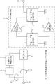
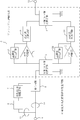
- FIG. FIG. 4 is a circuit configuration diagram showing the harmonic injection push-pull amplifier according to the first embodiment of the present invention.
- the push-pull amplifier circuit 5 is composed of unit amplifiers 1 and 2, an input side balanced / unbalanced conversion circuit 3 such as a balun connected to the input side and the output side thereof, and an output side balanced / unbalanced conversion circuit 4. Is done.
- the push-pull amplifier circuit 5 includes the input-side balanced / unbalanced conversion circuit 3, the unit amplifiers 1 and 2 connected to the input-side balanced / unbalanced conversion circuit 3, and the unit amplifiers 1 and 2 respectively.
- an output side balanced / unbalanced conversion circuit 4 is synthesized in which the outputs of the unit amplifiers 1 and 2 are combined.
- An amplitude phase adjustment circuit 7 for giving an appropriate amplitude and phase to the odd-order harmonic distortion signal and a coupling circuit 8 for synthesizing the basic signal and the odd-order harmonic distortion signal are provided.
- the basic signal input from the input port 9 is divided into two paths: a basic signal path 10 and a distorted signal path 11.
- the basic signal passing through the basic signal path 10 passes as it is.
- the distortion signal path 11 the odd-order harmonic distortion signal having an appropriate amplitude and phase is generated by the odd-order harmonic distortion signal generation circuit 6 and the amplitude phase adjustment circuit 7.
- the generated odd harmonic distortion signal and the basic signal are combined by the coupling circuit 8 and input to the balanced / unbalanced conversion circuit 3 of the push-pull amplifier circuit 5.
- the unit amplifiers 1 and 2 are inputted with the basic signals having opposite phases to each other and their odd harmonic distortion signals and amplified.
- the unit amplifiers 1 and 2 By appropriately selecting the amplitude and phase characteristics of the odd-order harmonic distortion signal in advance (in other words, by selecting a desired amplitude and phase set to reduce distortion), the unit amplifiers 1 and 2 The internally generated distortion signal component can be canceled, and the distortion signal appearing at the output port 12 can be reduced.
- the odd-order harmonic distortion signal generation circuit 6, the amplitude / phase adjustment circuit 7, and the coupling circuit 8 constitute a harmonic distortion signal generation circuit.
- the appropriate amplitude and phase of the odd-order harmonic distortion signal can be obtained for the odd-order harmonic distortion signal from the aforementioned equations (16) and (17).
- the harmonic injection push-pull amplifier includes the input-side balanced / unbalanced conversion circuit 3 and two units connected to the input-side balanced / unbalanced conversion circuit 3 and operating in opposite phases. It has amplifiers 1 and 2 and an output side balanced / unbalanced conversion circuit 4 in which the output sides of the unit amplifiers 1 and 2 are connected and the outputs of the unit amplifiers 1 and 2 are combined.
- Push-pull amplifier circuit, and a harmonic distortion signal generation circuit for inputting a harmonic distortion signal including an odd-order harmonic distortion signal of the basic signal to each of two unit amplifiers of the push-pull amplification circuit And the odd harmonic distortion signal is input to the two unit amplifiers 1 and 2 together with the basic signal to reduce distortion.
- the harmonic distortion signal generation circuit for inputting the harmonic distortion signal including the odd harmonic distortion signal of the basic signal of the present invention in other words, the odd harmonic distortion signal in the odd harmonic distortion signal generation circuit.
- the included harmonic distortion signal is, for example, a signal that includes at least an odd-order harmonic, corresponding to a third-order harmonic distortion signal generated when the basic input signal is multiplied by three.
- the harmonic distortion signal including the conventional even harmonic distortion signal specifically corresponds to, for example, a second harmonic distortion signal generated when the basic input signal is doubled.
- the intermodulation distortion component generated inside the amplifier can be canceled and distortion can be suppressed, but this is applied to a push-pull amplifier. Then you can't do that in principle.
- the intermodulation distortion component of the push-pull amplifier can be canceled and distortion can be suppressed.
- FIG. FIG. 5 is a circuit configuration diagram showing a harmonic injection push-pull amplifier according to the second embodiment of the present invention.
- the same numerals indicate the same or corresponding parts, and the description is omitted.
- a part of the input basic signal is extracted by using a multiplier 13 for generating the third harmonic in the odd harmonic distortion signal generating circuit 6 according to the first embodiment of FIG.
- a harmonic distortion signal is generated, and its operation and effect are the same as those of the first embodiment shown in FIG.
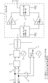
- FIG. FIG. 6 is a circuit configuration diagram showing a harmonic injection push-pull amplifier according to the third embodiment of the present invention.
- I and Q baseband signals are applied to the input port 9.
- the fundamental signal path 10 is loaded with a quadrature modulator 14, and the I and Q baseband signals are quadrature modulated with the fundamental signal frequency carrier ⁇ to generate a fundamental signal.
- an odd-order baseband distortion signal generation circuit 15 that generates an odd-order baseband distortion component from the input I and Q baseband signals, and the odd-order baseband distortion signal is input to an input basic signal frequency carrier wave.
- An odd-order harmonic quadrature modulation circuit 16 that performs quadrature modulation using an odd-order double frequency carrier wave 3 ⁇ of ⁇ is loaded.
- the odd-order baseband distortion component is quadrature modulated by the odd-order harmonic quadrature modulation circuit 16, thereby generating an odd-order harmonic distortion signal.
- the basic signal and the odd harmonic distortion signal are combined by the coupling circuit 8 and input to the push-pull amplifier circuit 5. Even with such a configuration, the same effect as that of the first embodiment shown in FIG. 4 can be obtained.
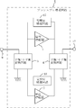
- FIG. FIG. 7 is a circuit configuration diagram showing a harmonic injection push-pull amplifier according to the fourth embodiment of the present invention.
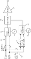
- Harmonic feedback circuits 17 and 18 for feeding back harmonic distortion signals including odd harmonic distortion signals with appropriate amplitude and phase between the input and output of the two unit amplifiers 1 and 2 of the push-pull amplifier circuit 5 are loaded. is doing. Thereby, an appropriate amplitude and phase are given to the harmonic distortion signal generated on the output side of the unit amplifiers 1 and 2 (in other words, a desired amplitude and phase set to reduce distortion are given).
- the unit amplifiers 1 and 2 are input again.
- the distortion of each of the unit amplifiers 1 and 2 can be simultaneously reduced for both the even-order and odd-order harmonic distortion signals, and as a result, the distortion signal appearing at the output port 12 can be reduced.
- the appropriate amplitude and phase fed back by the harmonic feedback circuits 17 and 18 can be obtained for the odd-order harmonic distortion signal from the aforementioned equations (16) and (17).
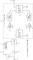
- FIG. FIG. 8 is a circuit configuration diagram showing a harmonic injection push-pull amplifier according to the fifth embodiment of the present invention.
- a different part from Embodiment 1 shown in FIG. 4 is mainly demonstrated.
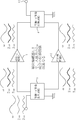
- a harmonic reflection circuit for reflecting one or both of the odd-order harmonic and the even-order harmonic at a desired and appropriate amplitude and phase on the output side of each of the two unit amplifiers 1 and 2 of the push-pull amplifier 5 19 and 20 are loaded.
- the basic signal component is synthesized as it is by the output side balanced / unbalanced conversion circuit 4 and outputted to the output port 12.
- the harmonic distortion signal components output from the unit amplifiers 1 and 2 are reflected at appropriate amplitudes and phases, and are combined again with the harmonic distortion signal components generated by the unit amplifiers 1 and 2, respectively. Distortion can be counteracted. Unlike the case of injecting harmonics from the input side, in this case, the distortion of each of the unit amplifiers 1 and 2 can be simultaneously reduced for both even-order and odd-order harmonic distortion signals. As a result, they appear at the output port 12. Distortion signals can be reduced. Note that the appropriate amplitude and phase reflected by the harmonic reflection circuits 19 and 20 can be obtained for the odd-order harmonic distortion signal from the aforementioned equations (16) and (17).
- FIG. 9 is a circuit configuration diagram showing a harmonic injection push-pull amplifier according to the sixth embodiment of the present invention.
- the wave feedback circuits 17 and 18 are provided at the same time. Even with such a configuration, the distortion of each of the unit amplifiers 1 and 2 can be simultaneously reduced for both the even-order and odd-order harmonic distortion signals, and as a result, the distortion signal appearing at the output port 12 can be reduced.
- the unit amplifier is not limited to a single-stage amplifier, and may have a multistage configuration.
- the unit amplifier may be a power combining type amplifier in which amplifying elements are arranged in parallel to achieve power combining.
- the harmonic injection microwave push-pull amplifier according to the present invention can also be used in combination with other distortion compensation circuits such as feed forward and digital predistorter.
- the partial configuration of each embodiment is not only a push-pull configuration amplifier but also a single-ended amplifier, a balanced amplifier, a corporate power combining amplifier, etc. that do not use a balanced / unbalanced conversion circuit due to its operating principle. Can also be applied.
Landscapes
- Engineering & Computer Science (AREA)
- Power Engineering (AREA)
- Physics & Mathematics (AREA)
- Nonlinear Science (AREA)
- Amplifiers (AREA)
Abstract
高調波注入プッシュプル増幅器に関し、平衡/不平衡変換回路3,4と、その平衡/不平衡変換回路3,4と接続され互いに逆相動作する2つの単位増幅器1,2とを有し、基本信号が入力されるプッシュプル増幅回路5において、2つの単位増幅器1,2のそれぞれに入力側から基本信号の奇数次高調波歪信号を含む高調波歪信号を入力する高調波歪信号発生回路を備え、基本信号と共に奇数次高調波歪信号を入力することにより低歪化を図るようにしたものである。
Description
本発明は、通信基地局の送信機などに用いられるプッシュプル増幅器に関し、基本信号と共にその高調波歪信号を入力することにより低歪化を図る高調波注入プッシュプル増幅器に係わるものである。
従来、増幅器の低歪化を図る手法として、増幅器の入力側から基本信号と共にその偶数次高調波歪信号を入力する方法が報告されている。図10は例えば非特許文献1に示された偶数次高調波注入により低歪化を図る従来の高調波注入増幅器を示す回路構成図である。入力されたI,Qベースバンド信号に対し、基本信号経路31ではI,Qベースバンド信号を搬送波角周波数ωで直交変調し基本信号を生成する。一方、歪信号経路32では、I,Qベースバンド信号を偶数次ベースバンド歪発生回路34で2次及び4次の偶数次歪相当の歪信号に変換し、次に、搬送波角周波数2ωを用いて直交変調し偶数次高調波歪信号を生成する。その偶数次高調波歪信号は、結合回路36で前記基本信号と合成されて増幅器37に入力される。増幅素子内部で発生した相互変調歪成分の一部が入力された前記偶数次高調波歪信号により打ち消されることにより増幅器37の低歪化を図るものである。なお、33は直交変調回路、35は直交変調回路である。
一般に通信基地局の送信機などに用いられる増幅器では、高出力・高効率性能の要求からバラン(balun)などの平衡/不平衡変換回路(balance-to-unbalance
transformer)を用いたプッシュプル増幅器が多く用いられる。しかし、従来の偶数次高調波歪信号を入力して歪補償を行う方式は、下記理由からプッシュプル構成の増幅器に用いることが困難な問題がある。
transformer)を用いたプッシュプル増幅器が多く用いられる。しかし、従来の偶数次高調波歪信号を入力して歪補償を行う方式は、下記理由からプッシュプル構成の増幅器に用いることが困難な問題がある。
図11は、プッシュプル増幅器の構成、及び基本信号を入力し増幅する場合の信号波形の様子を示す回路構成図である。1は単位増幅器A、2は単位増幅器Bである。3,4はそれぞれ平衡/不平衡変換回路である。各単位増幅器A,Bには
B級バイアスが印加され、飽和領域で動作しているものとして増幅された出力側の信号波形の様子を示している。搬送波角周波数がωである入力された基本信号はバランにより逆相で各単位増幅器A,Bに入力される。この結果、各単位増幅器A,Bで増幅された信号波形も互いに逆相となっている。
B級バイアスが印加され、飽和領域で動作しているものとして増幅された出力側の信号波形の様子を示している。搬送波角周波数がωである入力された基本信号はバランにより逆相で各単位増幅器A,Bに入力される。この結果、各単位増幅器A,Bで増幅された信号波形も互いに逆相となっている。
図12は、図11で増幅された信号波形をフーリエ級数展開して基本波及び高調波成分に分解したときの様子を示す説明図である。図12では、説明を簡単にするため、偶数次高調波として2次高調波までを、奇数次高調波として3次高調波までを示している。図12から分かるように、各単位増幅器A,Bで増幅された信号成分のうち、基本波及び3次高調波は、各単位増幅器A,Bの出力で互いに逆相になっている。これに対し、2次高調波は同相となっている。
次に、前記プッシュプル増幅器の入力側から、基本信号と共に、2次及び3次高調波信号を入力した場合の波形の様子を図13に示す。入力された基本波、2次、及び3次高調波は平衡/不平衡変換回路3により各単位増幅器A,Bに互いに逆相で入力される。一方、各単位増幅器A,Bの出力側の信号波形は、各単位増幅器A,Bに基本信号のみを入力した場合の出力信号波形をフーリエ級数展開して得られたものであり、図12の場合と同じものである。図13から、基本波及び3次高調波については、各単位増幅器A,Bで、入出力の波形の位相関係が等しくなっている。
一方、2次高調波については、単位増幅器Aと単位増幅器Bで、図に示すように、入出力の波形の位相関係が逆転している。このため、入力された2次高調波を増幅したものと、増幅器内部で発生した2次高調波とが、一方の単位増幅器A(又はB)では減算され歪が低減されても、他方の単位増幅器B(又はA)では加算され歪が増大することになる。このため、偶数次高調波を入力側より注入する従来の方法をプッシュプル増幅器に適用しても低歪化が図れない。
以上のように、通信基地局のような高出力・高効率な性能が要求される送信機用増幅器などに一般に用いられるプッシュプル増幅器では、低歪化を図るため偶数次高調波歪信号を基本信号と共に入力側から注入する従来の構成は適用できない問題がある。
若杉健市, 松原裕, 岩井遼太, 野島俊雄、"偶数次歪発生器を用いたデジタルプリディストーションの2GHz帯基礎実験"、信学技報、日本国、EMCJ2006-58,MW2006-114(2006-10)、pp.43-46(プリディストーション:predistortion)
本発明は、前記問題点に鑑みてなされたものであり、通信基地局のような高出力・高効率な性能が要求される送信機用増幅器などに一般に用いられるプッシュプル増幅回路においても、低歪化を図ることができる高調波注入プッシュプル増幅器を得ることを目的とするものである。
本発明の高調波注入プッシュプル増幅器は、平衡/不平衡変換回路と、その平衡/不平衡変換回路に接続され互いに逆相動作する2つの単位増幅器とを有し、基本信号が入力されるプッシュプル増幅回路において、2つの前記単位増幅器のそれぞれに入力側から前記基本信号の奇数次高調波歪信号を含む高調波歪信号を入力する高調波歪信号発生回路を備え、前記基本信号と共に前記奇数次高調波歪信号を入力することにより低歪化を図るようにしたものである。
本発明に係る高調波注入プッシュプル増幅器によれば、基本信号と共に奇数次高調波歪信号を入力することによりプッシュプル増幅回路の低歪化を図ることができる。
本発明の前記以外の目的、特徴、観点及び効果は、図面を参照する以下の本発明の詳細な説明から、さらに明らかになるであろう。
本発明の前記以外の目的、特徴、観点及び効果は、図面を参照する以下の本発明の詳細な説明から、さらに明らかになるであろう。
1,2 単位増幅器 3,4 平衡/不平衡変換回路
5 プッシュプル増幅回路 6 奇数次高調波歪信号発生回路
7 振幅位相調整回路 8 結合回路
9 入力ポート 10 基本信号経路
11 歪信号経路 12 出力ポート
13 てい倍器 14 直交変調器
15 奇数次ベースバンド歪信号生成回路 16 奇数次高調波直交変調回路
17,18 高調波帰還回路 19,20 高調波反射回路
5 プッシュプル増幅回路 6 奇数次高調波歪信号発生回路
7 振幅位相調整回路 8 結合回路
9 入力ポート 10 基本信号経路
11 歪信号経路 12 出力ポート
13 てい倍器 14 直交変調器
15 奇数次ベースバンド歪信号生成回路 16 奇数次高調波直交変調回路
17,18 高調波帰還回路 19,20 高調波反射回路
初めに、プッシュプル増幅回路の歪を低減できる原理を説明する。ここでは、奇数次高調波歪信号として特に3次高調波歪信号を考え、3次高調波歪信号に適切な振幅及び位相を与えて基本信号と共に入力することにより、プッシュプル増幅回路の歪を低減できることを説明する。
このためまず、図1を用いて、角周波数ω1,ω2の同相・同振幅の信号が、非線形動作する増幅器に入力された場合の、相互変調歪の発生について説明する。
このとき、増幅器の入力電圧vin及び出力電圧voutは以下のように表せる。
vout=g1vin+g2vin 2+g3vin 3+g4vin 4+g5vin 5+Λ -----------
(1)
ここで、g1は、基本信号に対する増幅率を表し、gi(i=2,3,4,5,Λ)は非線形歪の成分を表す。一般にgi(i=2,3,4,5,Λ)はiが増加するのに伴い小さくなる微小量である。
このとき、増幅器の入力電圧vin及び出力電圧voutは以下のように表せる。
vout=g1vin+g2vin 2+g3vin 3+g4vin 4+g5vin 5+Λ -----------
(1)
ここで、g1は、基本信号に対する増幅率を表し、gi(i=2,3,4,5,Λ)は非線形歪の成分を表す。一般にgi(i=2,3,4,5,Λ)はiが増加するのに伴い小さくなる微小量である。
ここで、入力電圧vinを次式で与える。
vin=x+y ------- (2)
x,yは角周波数ω1,ω2の基本信号電圧で、それぞれ以下で与えられる。
x=cosω1t ------- (3)
y=cosω2t ------- (4)
vin=x+y ------- (2)
x,yは角周波数ω1,ω2の基本信号電圧で、それぞれ以下で与えられる。
x=cosω1t ------- (3)
y=cosω2t ------- (4)
式(2)を式(1)に代入すると、右辺の各項の成分は以下となる。
g1vin=g1(x+y) -------- (5)
g2vin 2=g2(x2+2xy+y2) ---------
(6)
g3vin 3=g3(x3+3x2y+3xy2+y3) -------- (7)
g4vin 4=g4(x4+4x3y+6x2y2+4xy3+y4) -------
(8)
g5vin 5=g5(x5+5x4y+10x3y2+10x2y3+5xy4+y5) (9)
g1vin=g1(x+y) -------- (5)
g2vin 2=g2(x2+2xy+y2) ---------
(6)
g3vin 3=g3(x3+3x2y+3xy2+y3) -------- (7)
g4vin 4=g4(x4+4x3y+6x2y2+4xy3+y4) -------
(8)
g5vin 5=g5(x5+5x4y+10x3y2+10x2y3+5xy4+y5) (9)
式(5)は基本信号の増幅を示す。
式(6)~(9)の残りの項は、増幅器の非線形により発生するものである。このうち、増幅器の出力に設けたフィルタにより除去できない3次の相互変調歪IM3や5次の相互変調歪IM5などの奇数次相互変調歪が、帯域外スプリアス(spurious)の増大や信号品質の劣化などの問題を引き起こすため、その低減が必要となる。
ここで、IM3、IM5は、式(6)~(9)において、特に以下の成分により生じる。
IM3成分; g33x2y, g33xy2, g55x4y,
g510x3y2,
g510x2y3, g55xy4 ---------- (10)
IM5成分; g510x3y2, g510x2y3 ---------- (11)
次に、図2に示すように、基本信号と共に奇数次高調波歪信号を入力側から注入した場合について述べる。図2では、説明を簡単にするため、奇数次高調波歪信号を、3次の高調波としている。増幅器の入力電圧vin3及び出力電圧vout3は以下のように表せる。
vout3=g1vin3+g2vin3 2+g3vin3 3+g4vin3 4+g5vin3 5+Λ (12)
このとき、入力電圧vin3は次式で与えられる。
vin3=x+y+bx3+by3 ----- (13)
x3,y3は角周波数3ω1,3ω2の高調波成分の電圧で、それぞれ以下で与えられる。
x3=cos3ω1t -------- (14)
y3=cos3ω2t -------- (15)
vout3=g1vin3+g2vin3 2+g3vin3 3+g4vin3 4+g5vin3 5+Λ (12)
このとき、入力電圧vin3は次式で与えられる。
vin3=x+y+bx3+by3 ----- (13)
x3,y3は角周波数3ω1,3ω2の高調波成分の電圧で、それぞれ以下で与えられる。
x3=cos3ω1t -------- (14)
y3=cos3ω2t -------- (15)
式(13)を式(12)に代入し、前述と同様の方法でIM3、IM5成分を求めると、図3に示す結果が得られる。係数の大きな項に着目すると、bが次式を満足するように選ぶことによりIM3の低減が可能である。
g33x2y+g36bxx3y≒0 g33xy2+g36byy3x≒0
(16)
また、bが次式を満足するように選ぶことによりIM5の低減が可能である。
g510x3y2+g33by2x3≒0
g510x2y3+g33bx2y3≒0 -------
(17)
すなわち、奇数次高調波歪信号を入力することにより、IM3、IM5などの相互変調歪を低減することが可能である。
g33x2y+g36bxx3y≒0 g33xy2+g36byy3x≒0
(16)
また、bが次式を満足するように選ぶことによりIM5の低減が可能である。
g510x3y2+g33by2x3≒0
g510x2y3+g33bx2y3≒0 -------
(17)
すなわち、奇数次高調波歪信号を入力することにより、IM3、IM5などの相互変調歪を低減することが可能である。
実施の形態1.
図4は本発明の実施の形態1における高調波注入プッシュプル増幅器を示す回路構成図である。プッシュプル増幅回路5は、単位増幅器1,2、及びそれらの入力側と出力側にそれぞれ接続されたバランなどの入力側平衡/不平衡変換回路3,出力側平衡/不平衡変換回路4で構成される。換言すれば、プッシュプル増幅回路5は、入力側平衡/不平衡変換回路3、その入力側平衡/不平衡変換回路3にそれぞれ接続された単位増幅器1,2、及びそれらの単位増幅器1,2のそれぞれの出力側が接続されその単位増幅器1,2の出力が合成される出力側平衡/不平衡変換回路4で構成される。プッシュプル増幅回路5の入力側には、プッシュプル増幅回路5へ入力される基本信号の一部を取り出して、基本信号の奇数次高調波歪信号を生成する奇数次高調波歪信号発生回路6、その奇数次高調波歪信号に適切な振幅と位相を与える振幅位相調整回路7、及び基本信号と前記奇数次高調波歪信号とを合成する結合回路8を設けている。
図4は本発明の実施の形態1における高調波注入プッシュプル増幅器を示す回路構成図である。プッシュプル増幅回路5は、単位増幅器1,2、及びそれらの入力側と出力側にそれぞれ接続されたバランなどの入力側平衡/不平衡変換回路3,出力側平衡/不平衡変換回路4で構成される。換言すれば、プッシュプル増幅回路5は、入力側平衡/不平衡変換回路3、その入力側平衡/不平衡変換回路3にそれぞれ接続された単位増幅器1,2、及びそれらの単位増幅器1,2のそれぞれの出力側が接続されその単位増幅器1,2の出力が合成される出力側平衡/不平衡変換回路4で構成される。プッシュプル増幅回路5の入力側には、プッシュプル増幅回路5へ入力される基本信号の一部を取り出して、基本信号の奇数次高調波歪信号を生成する奇数次高調波歪信号発生回路6、その奇数次高調波歪信号に適切な振幅と位相を与える振幅位相調整回路7、及び基本信号と前記奇数次高調波歪信号とを合成する結合回路8を設けている。
以下動作について説明する。入力ポート9から入力された基本信号は、基本信号経路10及び歪信号経路11の2つの経路に分割される。基本信号経路10を通る基本信号はそのまま通過する。他方、歪信号経路11では、奇数次高調波歪信号発生回路6及び振幅位相調整回路7により、適切な振幅と位相を有する奇数次高調波歪信号が生成される。生成された奇数次高調波歪信号と前記基本信号とは結合回路8で合成され、プッシュプル増幅回路5の平衡/不平衡変換回路3に入力される。平衡/不平衡変換回路3を経て、各単位増幅器1,2に互いに逆相の基本信号とその奇数次高調波歪信号とが入力され増幅される。あらかじめ奇数次高調波歪信号の振幅と位相特性を適切に選ぶことにより(換言すれば、歪を低減するように設定された所望な振幅と位相を選ぶことにより)、各単位増幅器1,2の内部で発生した歪信号成分を打ち消すことができ、出力ポート12に現れる歪信号を低減することができる。なお、奇数次高調波歪信号発生回路6、振幅位相調整回路7及び結合回路8で高調波歪信号発生回路が構成される。奇数次高調波歪信号の適切な振幅と位相は、前述の式(16)(17)より奇数次高調波歪信号について求めることができる。
このように、実施の形態1の高調波注入プッシュプル増幅器は、入力側平衡/不平衡変換回路3と、その入力側平衡/不平衡変換回路3にそれぞれ接続され互いに逆相動作する2つの単位増幅器1,2と、それらの単位増幅器1,2のそれぞれの出力側が接続されその単位増幅器1,2の出力が合成される出力側平衡/不平衡変換回路4とを有し、基本信号が入力されるプッシュプル増幅回路、及び、前記プッシュプル増幅回路の2つの単位増幅器のそれぞれに入力側から前記基本信号の奇数次高調波歪信号を含む高調波歪信号を入力する高調波歪信号発生回路を備え、前記基本信号と共に前記奇数次高調波歪信号を2つの前記単位増幅器1,2にそれぞれ入力することにより低歪化を図るようにしたものである。
なお、本発明の基本信号の奇数次高調波歪信号を含む高調波歪信号を入力する高調波歪信号発生回路、換言すれば、奇数次高調波歪信号発生回路における奇数次高調波歪信号を含む高調波歪信号は,具体的に言うと、例えば、基本入力信号を3てい倍した場合に発生する3次高調波歪信号がそれに相当し、少なくとも奇数次高調波を含んだ信号である。一方、従来の偶数次高調波歪信号を含む高調波歪信号は、具体的に言うと、例えば、基本入力信号を2てい倍した場合に発生する2次高調波歪信号がそれに相当する。従来技術では、シングルエンド増幅器に、偶数次高調波歪信号を入力することにより、増幅器内部で発生する相互変調歪成分を打ち消し歪を抑圧することができるが,これをプッシュプル増幅器に適用しようとすると原理的にそれができない。これに対して、奇数次高調波歪信号を用いる場合には,プッシュプル増幅器の相互変調歪成分を打ち消し歪を抑圧することが可能となる。
なお、本発明の基本信号の奇数次高調波歪信号を含む高調波歪信号を入力する高調波歪信号発生回路、換言すれば、奇数次高調波歪信号発生回路における奇数次高調波歪信号を含む高調波歪信号は,具体的に言うと、例えば、基本入力信号を3てい倍した場合に発生する3次高調波歪信号がそれに相当し、少なくとも奇数次高調波を含んだ信号である。一方、従来の偶数次高調波歪信号を含む高調波歪信号は、具体的に言うと、例えば、基本入力信号を2てい倍した場合に発生する2次高調波歪信号がそれに相当する。従来技術では、シングルエンド増幅器に、偶数次高調波歪信号を入力することにより、増幅器内部で発生する相互変調歪成分を打ち消し歪を抑圧することができるが,これをプッシュプル増幅器に適用しようとすると原理的にそれができない。これに対して、奇数次高調波歪信号を用いる場合には,プッシュプル増幅器の相互変調歪成分を打ち消し歪を抑圧することが可能となる。
実施の形態2.
図5は本発明の実施の形態2における高調波注入プッシュプル増幅器を示す回路構成図である。なお、各図中において、同一符号は同一又は相当部分を示し、説明を省略する。図4の実施の形態1による奇数次高調波歪信号発生回路6の部分に、3次高調波を発生するてい倍器13を用いて、入力される基本信号の一部を取り出してその奇数次高調波歪信号を生成するもので、その動作、及び効果は図4の実施の形態1の場合と同じである。
図5は本発明の実施の形態2における高調波注入プッシュプル増幅器を示す回路構成図である。なお、各図中において、同一符号は同一又は相当部分を示し、説明を省略する。図4の実施の形態1による奇数次高調波歪信号発生回路6の部分に、3次高調波を発生するてい倍器13を用いて、入力される基本信号の一部を取り出してその奇数次高調波歪信号を生成するもので、その動作、及び効果は図4の実施の形態1の場合と同じである。
実施の形態3.
図6は本発明の実施の形態3における高調波注入プッシュプル増幅器を示す回路構成図である。ここでは、入力ポート9にI,Qベースバンド信号が印加される。基本信号経路10には直交変調器14が装荷され、I,Qベースバンド信号は基本信号周波数搬送波ωで直交変調され基本信号が生成される。一方、歪信号経路11では、入力したI,Qベースバンド信号から奇数次ベースバンド歪成分を生成する奇数次ベースバンド歪信号生成回路15と、その奇数次ベースバンド歪信号を入力基本信号周波数搬送波ωの奇数次倍周波数搬送波3ωを用いて直交変調する奇数次高調波直交変調回路16が装荷されている。奇数次ベースバンド歪成分は、奇数次高調波直交変調回路16で直交変調され、これにより、奇数次高調波歪信号が生成される。前記基本信号と前記奇数次高調波歪信号とは結合回路8で合成され、プッシュプル増幅回路5へ入力される。このような、構成にしても、図4に示す実施の形態1の場合と同様な効果を得ることができる。
図6は本発明の実施の形態3における高調波注入プッシュプル増幅器を示す回路構成図である。ここでは、入力ポート9にI,Qベースバンド信号が印加される。基本信号経路10には直交変調器14が装荷され、I,Qベースバンド信号は基本信号周波数搬送波ωで直交変調され基本信号が生成される。一方、歪信号経路11では、入力したI,Qベースバンド信号から奇数次ベースバンド歪成分を生成する奇数次ベースバンド歪信号生成回路15と、その奇数次ベースバンド歪信号を入力基本信号周波数搬送波ωの奇数次倍周波数搬送波3ωを用いて直交変調する奇数次高調波直交変調回路16が装荷されている。奇数次ベースバンド歪成分は、奇数次高調波直交変調回路16で直交変調され、これにより、奇数次高調波歪信号が生成される。前記基本信号と前記奇数次高調波歪信号とは結合回路8で合成され、プッシュプル増幅回路5へ入力される。このような、構成にしても、図4に示す実施の形態1の場合と同様な効果を得ることができる。
実施の形態4.
図7は本発明の実施の形態4における高調波注入プッシュプル増幅器を示す回路構成図である。プッシュプル増幅回路5の2つの単位増幅器1,2のそれぞれの入出力間に奇数次高調波歪信号を含む高調波歪信号を適切な振幅と位相で帰還する高調波帰還回路17,18を装荷している。これにより、単位増幅器1,2の出力側に発生した高調波歪信号を適切な振幅と位相を与えて(換言すれば、歪を低減するように設定された所望な振幅と位相を与えて)、再び単位増幅器1,2に入力している。この場合、偶数次及び奇数次高調波歪信号のいずれについても、各単位増幅器1,2の歪を同時に低減でき、この結果、出力ポート12に現れる歪信号を低減することができる。なお、高調波帰還回路17,18で帰還される適切な振幅と位相は、前述の式(16)(17)より奇数次高調波歪信号について求めることができる。
図7は本発明の実施の形態4における高調波注入プッシュプル増幅器を示す回路構成図である。プッシュプル増幅回路5の2つの単位増幅器1,2のそれぞれの入出力間に奇数次高調波歪信号を含む高調波歪信号を適切な振幅と位相で帰還する高調波帰還回路17,18を装荷している。これにより、単位増幅器1,2の出力側に発生した高調波歪信号を適切な振幅と位相を与えて(換言すれば、歪を低減するように設定された所望な振幅と位相を与えて)、再び単位増幅器1,2に入力している。この場合、偶数次及び奇数次高調波歪信号のいずれについても、各単位増幅器1,2の歪を同時に低減でき、この結果、出力ポート12に現れる歪信号を低減することができる。なお、高調波帰還回路17,18で帰還される適切な振幅と位相は、前述の式(16)(17)より奇数次高調波歪信号について求めることができる。
実施の形態5.
図8は本発明の実施の形態5における高調波注入プッシュプル増幅器を示す回路構成図である。図4に示す実施の形態1に対して異なる部分を主に説明する。プッシュプル増幅器5の2つの単位増幅器1,2のそれぞれの出力側に、奇数次高調波及び偶数次高調波の一方又は両方を設定された所望で適切な振幅及び位相で反射させる高調波反射回路19,20を装荷している。各単位増幅器1,2からの出力のうち、基本信号成分はそのまま出力側平衡/不平衡変換回路4で合成され出力ポート12に出力される。一方、各単位増幅器1,2から出力された高調波歪信号成分はそれぞれ適切な振幅と位相で反射され、各単位増幅器1,2で発生した高調波歪信号成分と再び結合されることにより、歪を打ち消すことができる。入力側から高調波を注入する場合と異なり、この場合、偶数次及び奇数次高調波歪信号のいずれについても、各単位増幅器1,2の歪を同時に低減でき、この結果、出力ポート12に現れる歪信号を低減することができる。なお、高調波反射回路19,20で反射される適切な振幅と位相は、前述の式(16)(17)より奇数次高調波歪信号について求めることができる。
図8は本発明の実施の形態5における高調波注入プッシュプル増幅器を示す回路構成図である。図4に示す実施の形態1に対して異なる部分を主に説明する。プッシュプル増幅器5の2つの単位増幅器1,2のそれぞれの出力側に、奇数次高調波及び偶数次高調波の一方又は両方を設定された所望で適切な振幅及び位相で反射させる高調波反射回路19,20を装荷している。各単位増幅器1,2からの出力のうち、基本信号成分はそのまま出力側平衡/不平衡変換回路4で合成され出力ポート12に出力される。一方、各単位増幅器1,2から出力された高調波歪信号成分はそれぞれ適切な振幅と位相で反射され、各単位増幅器1,2で発生した高調波歪信号成分と再び結合されることにより、歪を打ち消すことができる。入力側から高調波を注入する場合と異なり、この場合、偶数次及び奇数次高調波歪信号のいずれについても、各単位増幅器1,2の歪を同時に低減でき、この結果、出力ポート12に現れる歪信号を低減することができる。なお、高調波反射回路19,20で反射される適切な振幅と位相は、前述の式(16)(17)より奇数次高調波歪信号について求めることができる。
実施の形態6.
図9は本発明の実施の形態6における高調波注入プッシュプル増幅器を示す回路構成図である。図8に示す実施の形態5の構成における奇数次高調波歪信号発生回路6、振幅位相調整回路7、結合回路8、及び高周波反射回路19,20と、図7の実施形態4の構成における高調波帰還回路17,18とを同時に設ける構成としたものである。このような構成でも、偶数次及び奇数次高調波歪信号のいずれについても、各単位増幅器1,2の歪を同時に低減でき、この結果、出力ポート12に現れる歪信号を低減することができる。
図9は本発明の実施の形態6における高調波注入プッシュプル増幅器を示す回路構成図である。図8に示す実施の形態5の構成における奇数次高調波歪信号発生回路6、振幅位相調整回路7、結合回路8、及び高周波反射回路19,20と、図7の実施形態4の構成における高調波帰還回路17,18とを同時に設ける構成としたものである。このような構成でも、偶数次及び奇数次高調波歪信号のいずれについても、各単位増幅器1,2の歪を同時に低減でき、この結果、出力ポート12に現れる歪信号を低減することができる。
以上の説明において、単位増幅器は1段増幅器に限らず多段構成であってもよい。また、単位増幅器は並列に増幅素子を配置して電力合成を図った電力合成形増幅器であってもよい。また、本発明による高調波注入マイクロ波プッシュプル増幅器は、フィードフォワードやデジタルプリディストータなどの他の歪補償回路と組み合わせて用いることもできる。
また、各実施の形態の部分構成は、その動作原理から、プッシュプル構成の増幅器だけでなく、平衡/不平衡変換回路を用いないシングルエンド形増幅器、バランス形増幅器、コーポレート電力合成形増幅器などにも応用することもできる。
また、各実施の形態の部分構成は、その動作原理から、プッシュプル構成の増幅器だけでなく、平衡/不平衡変換回路を用いないシングルエンド形増幅器、バランス形増幅器、コーポレート電力合成形増幅器などにも応用することもできる。
本発明の各種の変形又は変更は、関連する熟練技術者が、この発明の範囲と精神を逸脱しない中で実現可能であり、この明細書に記載された各実施の形態には制限されないことと理解されるべきである。
Claims (6)
- 平衡/不平衡変換回路と、その平衡/不平衡変換回路とそれぞれ接続され互いに逆相動作する2つの単位増幅器とを有し、基本信号が入力されるプッシュプル増幅回路、
及び、前記プッシュプル増幅回路の2つの単位増幅器のそれぞれに入力側から前記基本信号の奇数次高調波歪信号を含む高調波歪信号を入力する高調波歪信号発生回路を備え、
前記基本信号と共に前記奇数次高調波歪信号を入力することにより低歪化を図るようにしたことを特徴とする高調波注入プッシュプル増幅器。 - 請求項1記載の高調波注入プッシュプル増幅器であって、
前記高調波歪信号発生回路は、入力される前記基本信号の一部を取り出してその奇数次高調波歪信号を生成する奇数次高調波歪信号発生回路、生成されたその奇数次高調波歪信号に適切な振幅と位相を与える振幅位相調整回路、及び前記基本信号と前記振幅位相調整回路の出力である前記奇数次高調波歪信号とを合成する結合回路で構成され、
前記結合回路で合成された前記基本信号と前記奇数次高調波歪信号とを前記プッシュプル増幅回路の入力側から入力することを特徴とする高調波注入プッシュプル増幅器。 - 請求項1記載の高調波注入プッシュプル増幅器であって、
前記高調波歪信号発生回路は、入力される前記基本信号の一部を取り出してその奇数次高調波歪信号を生成するてい倍器、生成されたその奇数次高調波歪信号に適切な振幅と位相を与える振幅位相調整回路、及び前記基本信号と前記振幅位相調整回路の出力である前記奇数次高調波歪信号とを合成する結合回路で構成され、
前記結合回路で合成された前記基本信号と前記奇数次高調波歪信号とを前記プッシュプル増幅回路の入力側から入力することを特徴とする高調波注入プッシュプル増幅器。 - 請求項1記載の高調波注入プッシュプル増幅器であって、
前記高調波歪信号発生回路は、
入力されるベースバンド信号が基本信号周波数搬送波で直交変調され基本信号が生成される直交変調器、
入力される前記ベースバンド信号から奇数次ベースバンド歪成分を生成する奇数次ベースバンド歪信号生成回路、
前記奇数次ベースバンド歪信号生成回路で生成された奇数次ベースバンド歪信号が前記基本信号周波数搬送波の奇数次倍周波数搬送波を用いて直交変調され奇数次高調波歪信号が生成される奇数次高調波直交変調回路、
及び前記直交変調器で生成された前記基本信号と前記奇数次高調波直交変調回路で生成された前記奇数次高調波歪信号とを合成する結合回路で構成され、
合成された前記結合回路の出力を前記プッシュプル増幅回路に入力するようにしたことを特徴とする高調波注入プッシュプル増幅器。 - 請求項1記載の高調波注入プッシュプル増幅器であって、
前記高調波歪信号発生回路は、前記単位増幅器のそれぞれの出力側に発生した高調波を適切な振幅と位相で前記単位増幅器のそれぞれの入力側に帰還させる高調波帰還回路で構成されたことを特徴とする高調波注入プッシュプル増幅器。 - 請求項1~請求項5のいずれか1項に記載の高調波注入プッシュプル増幅器であって、2つの前記単位増幅器のそれぞれの出力側に、奇数次高調波歪信号及び偶数次高調波歪信号の少なくともいずれか一方を適切な振幅と位相で反射させる高調波歪反射回路を備えたことを特徴とする高調波注入プッシュプル増幅器。
Priority Applications (2)
| Application Number | Priority Date | Filing Date | Title |
|---|---|---|---|
| JP2009516439A JPWO2010032283A1 (ja) | 2008-09-16 | 2008-09-16 | 高調波注入プッシュプル増幅器 |
| PCT/JP2008/066653 WO2010032283A1 (ja) | 2008-09-16 | 2008-09-16 | 高調波注入プッシュプル増幅器 |
Applications Claiming Priority (1)
| Application Number | Priority Date | Filing Date | Title |
|---|---|---|---|
| PCT/JP2008/066653 WO2010032283A1 (ja) | 2008-09-16 | 2008-09-16 | 高調波注入プッシュプル増幅器 |
Publications (1)
| Publication Number | Publication Date |
|---|---|
| WO2010032283A1 true WO2010032283A1 (ja) | 2010-03-25 |
Family
ID=42039137
Family Applications (1)
| Application Number | Title | Priority Date | Filing Date |
|---|---|---|---|
| PCT/JP2008/066653 Ceased WO2010032283A1 (ja) | 2008-09-16 | 2008-09-16 | 高調波注入プッシュプル増幅器 |
Country Status (2)
| Country | Link |
|---|---|
| JP (1) | JPWO2010032283A1 (ja) |
| WO (1) | WO2010032283A1 (ja) |
Cited By (4)
| Publication number | Priority date | Publication date | Assignee | Title |
|---|---|---|---|---|
| JP2013090166A (ja) * | 2011-10-19 | 2013-05-13 | Wave Technology Inc | バラン |
| JP2016076752A (ja) * | 2014-10-02 | 2016-05-12 | 株式会社Wave Technology | プシュプル電力増幅器 |
| JP2016530820A (ja) * | 2013-08-19 | 2016-09-29 | アリス エンタープライジズ インコーポレイテッドARRIS Enterprises, Inc. | 順方向データ・コンテンツによって電力消費が駆動される、光ファイバ・ノード |
| CN115327237A (zh) * | 2022-07-12 | 2022-11-11 | 苏州湛云科技有限公司 | 一种可扩展电池阻抗快速测量系统和方法 |
Citations (2)
| Publication number | Priority date | Publication date | Assignee | Title |
|---|---|---|---|---|
| JPH08139535A (ja) * | 1994-11-11 | 1996-05-31 | Fujitsu Ltd | 高効率の電力増幅器 |
| JPH09102718A (ja) * | 1995-10-06 | 1997-04-15 | Yagi Antenna Co Ltd | 高周波増幅装置 |
Family Cites Families (4)
| Publication number | Priority date | Publication date | Assignee | Title |
|---|---|---|---|---|
| JP2003023324A (ja) * | 2001-07-06 | 2003-01-24 | Matsushita Electric Ind Co Ltd | 増幅回路 |
| JP2004048174A (ja) * | 2002-07-09 | 2004-02-12 | Hitachi Kokusai Electric Inc | 電力増幅器 |
| JP4868433B2 (ja) * | 2004-02-09 | 2012-02-01 | ソニー・エリクソン・モバイルコミュニケーションズ株式会社 | 歪み補償装置および歪み補償機能付き電力増幅装置 |
| JP4671622B2 (ja) * | 2004-04-30 | 2011-04-20 | ソニー・エリクソン・モバイルコミュニケーションズ株式会社 | 歪み補償電力増幅装置 |
-
2008
- 2008-09-16 WO PCT/JP2008/066653 patent/WO2010032283A1/ja not_active Ceased
- 2008-09-16 JP JP2009516439A patent/JPWO2010032283A1/ja active Pending
Patent Citations (2)
| Publication number | Priority date | Publication date | Assignee | Title |
|---|---|---|---|---|
| JPH08139535A (ja) * | 1994-11-11 | 1996-05-31 | Fujitsu Ltd | 高効率の電力増幅器 |
| JPH09102718A (ja) * | 1995-10-06 | 1997-04-15 | Yagi Antenna Co Ltd | 高周波増幅装置 |
Cited By (6)
| Publication number | Priority date | Publication date | Assignee | Title |
|---|---|---|---|---|
| JP2013090166A (ja) * | 2011-10-19 | 2013-05-13 | Wave Technology Inc | バラン |
| JP2016530820A (ja) * | 2013-08-19 | 2016-09-29 | アリス エンタープライジズ インコーポレイテッドARRIS Enterprises, Inc. | 順方向データ・コンテンツによって電力消費が駆動される、光ファイバ・ノード |
| US10135396B2 (en) | 2013-08-19 | 2018-11-20 | Arris Enterprises Llc | Fiber-optic node with forward data content driven power consumption |
| US10749475B2 (en) | 2013-08-19 | 2020-08-18 | Arris Enterprises Llc | Fiber-optic node with forward data content driven power consumption |
| JP2016076752A (ja) * | 2014-10-02 | 2016-05-12 | 株式会社Wave Technology | プシュプル電力増幅器 |
| CN115327237A (zh) * | 2022-07-12 | 2022-11-11 | 苏州湛云科技有限公司 | 一种可扩展电池阻抗快速测量系统和方法 |
Also Published As
| Publication number | Publication date |
|---|---|
| JPWO2010032283A1 (ja) | 2012-02-02 |
Similar Documents
| Publication | Publication Date | Title |
|---|---|---|
| US6181199B1 (en) | Power IQ modulation systems and methods | |
| US9438186B2 (en) | Power amplifier with envelope injection | |
| CN107070467B (zh) | 模拟rf预失真器和非线性分离器 | |
| US8179957B2 (en) | Quadrature pulse-width modulation methods and apparatus | |
| US6757338B1 (en) | Predistortion linearizer using even order intermodulation components | |
| JPWO2010032283A1 (ja) | 高調波注入プッシュプル増幅器 | |
| US8542769B2 (en) | High output power digital TX | |
| CN101110595B (zh) | 多级linc发射器 | |
| JP2746130B2 (ja) | 非線形特性発生回路 | |
| Chung et al. | Frequency doubler based outphasing system for millimeter wave vector signal generation | |
| US8526536B2 (en) | Quad LINC transmitter with switchable Chireix amplifiers | |
| JP2000286643A (ja) | 周波数変換回路 | |
| US8213883B1 (en) | Additive pre-distortion for linearization | |
| JP5731325B2 (ja) | 変調器およびそれを用いる増幅器 | |
| JP2000183764A (ja) | 出力回路 | |
| JP2016076752A (ja) | プシュプル電力増幅器 | |
| JP2012205018A (ja) | 高出力電力増幅器 | |
| RU2438241C2 (ru) | Формирователь радиосигналов с цифровым линеаризатором | |
| Sobhy et al. | A multiphase multipath technique with digital phase shifters for harmonic distortion cancellation | |
| KR100837243B1 (ko) | 주파수 체배기의 사전 왜곡 선형화 장치 및 이를 이용한이중 모드 송신기 | |
| JP7542773B2 (ja) | 低歪み増幅器 | |
| JPH11112433A (ja) | Fm変調器 | |
| JP2008172352A (ja) | 高周波増幅回路 | |
| JP2008124910A (ja) | 高周波増幅回路 | |
| JP2531663B2 (ja) | 進行波管増幅回路 |
Legal Events
| Date | Code | Title | Description |
|---|---|---|---|
| WWE | Wipo information: entry into national phase |
Ref document number: 2009516439 Country of ref document: JP |
|
| 121 | Ep: the epo has been informed by wipo that ep was designated in this application |
Ref document number: 08810703 Country of ref document: EP Kind code of ref document: A1 |
|
| NENP | Non-entry into the national phase |
Ref country code: DE |
|
| 122 | Ep: pct application non-entry in european phase |
Ref document number: 08810703 Country of ref document: EP Kind code of ref document: A1 |