WO2010016319A1 - 画像処理装置、表示装置、画像処理方法、プログラム、及び、記録媒体 - Google Patents
画像処理装置、表示装置、画像処理方法、プログラム、及び、記録媒体 Download PDFInfo
- Publication number
- WO2010016319A1 WO2010016319A1 PCT/JP2009/060087 JP2009060087W WO2010016319A1 WO 2010016319 A1 WO2010016319 A1 WO 2010016319A1 JP 2009060087 W JP2009060087 W JP 2009060087W WO 2010016319 A1 WO2010016319 A1 WO 2010016319A1
- Authority
- WO
- WIPO (PCT)
- Prior art keywords
- pixel
- image data
- upscaling
- redistribution
- divided
- Prior art date
- Legal status (The legal status is an assumption and is not a legal conclusion. Google has not performed a legal analysis and makes no representation as to the accuracy of the status listed.)
- Ceased
Links
Images





Classifications
-
- H—ELECTRICITY
- H04—ELECTRIC COMMUNICATION TECHNIQUE
- H04N—PICTORIAL COMMUNICATION, e.g. TELEVISION
- H04N1/00—Scanning, transmission or reproduction of documents or the like, e.g. facsimile transmission; Details thereof
- H04N1/40—Picture signal circuits
- H04N1/40068—Modification of image resolution, i.e. determining the values of picture elements at new relative positions
-
- G—PHYSICS
- G09—EDUCATION; CRYPTOGRAPHY; DISPLAY; ADVERTISING; SEALS
- G09G—ARRANGEMENTS OR CIRCUITS FOR CONTROL OF INDICATING DEVICES USING STATIC MEANS TO PRESENT VARIABLE INFORMATION
- G09G3/00—Control arrangements or circuits, of interest only in connection with visual indicators other than cathode-ray tubes
- G09G3/20—Control arrangements or circuits, of interest only in connection with visual indicators other than cathode-ray tubes for presentation of an assembly of a number of characters, e.g. a page, by composing the assembly by combination of individual elements arranged in a matrix no fixed position being assigned to or needed to be assigned to the individual characters or partial characters
- G09G3/34—Control arrangements or circuits, of interest only in connection with visual indicators other than cathode-ray tubes for presentation of an assembly of a number of characters, e.g. a page, by composing the assembly by combination of individual elements arranged in a matrix no fixed position being assigned to or needed to be assigned to the individual characters or partial characters by control of light from an independent source
- G09G3/36—Control arrangements or circuits, of interest only in connection with visual indicators other than cathode-ray tubes for presentation of an assembly of a number of characters, e.g. a page, by composing the assembly by combination of individual elements arranged in a matrix no fixed position being assigned to or needed to be assigned to the individual characters or partial characters by control of light from an independent source using liquid crystals
- G09G3/3611—Control of matrices with row and column drivers
- G09G3/3648—Control of matrices with row and column drivers using an active matrix
-
- G—PHYSICS
- G09—EDUCATION; CRYPTOGRAPHY; DISPLAY; ADVERTISING; SEALS
- G09G—ARRANGEMENTS OR CIRCUITS FOR CONTROL OF INDICATING DEVICES USING STATIC MEANS TO PRESENT VARIABLE INFORMATION
- G09G2320/00—Control of display operating conditions
- G09G2320/02—Improving the quality of display appearance
- G09G2320/0271—Adjustment of the gradation levels within the range of the gradation scale, e.g. by redistribution or clipping
-
- G—PHYSICS
- G09—EDUCATION; CRYPTOGRAPHY; DISPLAY; ADVERTISING; SEALS
- G09G—ARRANGEMENTS OR CIRCUITS FOR CONTROL OF INDICATING DEVICES USING STATIC MEANS TO PRESENT VARIABLE INFORMATION
- G09G2320/00—Control of display operating conditions
- G09G2320/02—Improving the quality of display appearance
- G09G2320/028—Improving the quality of display appearance by changing the viewing angle properties, e.g. widening the viewing angle, adapting the viewing angle to the view direction
-
- G—PHYSICS
- G09—EDUCATION; CRYPTOGRAPHY; DISPLAY; ADVERTISING; SEALS
- G09G—ARRANGEMENTS OR CIRCUITS FOR CONTROL OF INDICATING DEVICES USING STATIC MEANS TO PRESENT VARIABLE INFORMATION
- G09G2340/00—Aspects of display data processing
- G09G2340/04—Changes in size, position or resolution of an image
- G09G2340/0407—Resolution change, inclusive of the use of different resolutions for different screen areas
Definitions
- the present invention relates to an image processing apparatus and an image processing method for upscaling the resolution of input image data to a high resolution.
- Patent Document 1 For example, a pixel division method described in Patent Document 1 is generally known as a method for solving such problems related to viewing angle characteristics.
- JP-A-4-102830 Publication Date: April 3, 1992
- liquid crystal display panel capable of generating a high-definition image by performing the upscaling process and improving the viewing angle has not been realized yet.
- the present invention has been made in view of the above problems, and an object thereof is to generate a high-definition image and improve the viewing angle in an image processing apparatus that converts the resolution of input image data to a high resolution.
- An object of the present invention is to provide an image processing apparatus that can be realized.
- an image processing apparatus is an image processing apparatus including an upscaling processing unit for upscaling the resolution of input image data to a high resolution.
- a redistribution processing unit that redistributes the gradation values of each of the plurality of divided pixels upscaled by the upscaling processing unit corresponding to the pixels among the plurality of divided pixels is provided.
- the gradation values of each of the plurality of upscaled divided pixels corresponding to one pixel of the input image data can be redistributed among the plurality of divided pixels. Therefore, it is possible to set the gradation value of each divided pixel to a gradation value at which a high-definition image can be obtained while improving the viewing angle by pixel division. That is, it is possible to simultaneously improve the viewing angle and increase the definition of the display image.
- the gradation value redistributed in the redistribution processing unit is determined according to the luminance and the pixel size.
- the redistribution processing unit includes the luminance represented by the image data of each of the plurality of divided pixels upscaled by the upscaling processing unit corresponding to one pixel of the input image data, It is preferable to redistribute the gradation values of each divided pixel after upscaling so that the luminance represented by the image data after redistribution of each of the plurality of divided pixels becomes equal to each other.
- the image processing apparatus of the present invention includes an upscaling processing unit for upscaling the resolution of input image data to a high resolution.
- a redistribution processing unit that redistributes gradation values of each of the divided pixels among the plurality of divided pixels is provided.
- the image processing device can be applied to a display device in which one pixel is composed of RGB sub-pixels, and the above-described effects can be obtained.
- the redistribution processing unit is represented by image data of each of a plurality of divided pixels corresponding to each sub-pixel upscaled by the upscaling processing unit in one pixel of input image data. It is preferable to redistribute the gradation values of each divided pixel after upscaling so that the luminance to be obtained and the luminance represented by the image data after redistribution of each of the plurality of divided pixels are equal to each other.
- the display image is improved in definition and the viewing angle is improved without changing the luminance before and after the redistribution of the upscaled image data. Can be realized.
- the redistribution processing unit redistributes the gradation value of each divided pixel after the upscaling based on the distribution ratio set for each sub pixel in one pixel of the input image data. It is preferable to do.
- the redistribution ratio can be changed for each sub-pixel.
- pixels that have a small contribution to luminance can be redistributed with a larger luminance difference, so the display image can be refined and the viewing angle improved without changing the luminance before and after redistribution.
- the effect can be further improved.
- the display device of the present invention includes any one of the image processing devices described above and a display unit that displays an image upscaled by the image processing device.
- a high-definition image can be generated and the viewing angle can be improved.
- the image processing method of the present invention is an image processing method including an upscaling process step for upscaling the resolution of input image data to a high resolution, wherein the upscaling process step corresponds to one pixel of the input image data. And a redistribution processing step of redistributing the gradation values of the plurality of divided pixels upscaled among the plurality of divided pixels.
- the image processing method it is possible to obtain the effect produced by the image processing apparatus. That is, according to the image processing method, a high-definition image can be generated and the viewing angle can be improved.
- the luminance represented by the image data of each of the plurality of divided pixels upscaled in the upscaling processing step corresponding to one pixel of the input image data, It is preferable to redistribute the gradation values of each divided pixel after upscaling so that the luminance represented by the image data after redistribution of each of the divided pixels becomes equal to each other.
- the image processing method of the present invention includes an upscale processing step for upscaling the resolution of input image data to a high resolution, and the upscaled image is divided into subpixels each corresponding to RGB.
- the image processing method can be applied to a display device in which one pixel is composed of RGB sub-pixels, and the above-described effects can be obtained.
- one pixel of the input image data is represented by image data of each of the plurality of divided pixels corresponding to the sub-pixels upscaled in the upscaling processing step. It is preferable to redistribute the gradation values of each of the divided pixels after the upscaling so that the luminance of the divided pixels and the luminance represented by the image data after redistribution of each of the plurality of divided pixels are equal to each other.
- the display image is improved in definition and the viewing angle is improved without changing the luminance before and after the redistribution of the upscaled image data. Can be realized.
- the image processing apparatus may be realized by a computer.
- Possible recording media are also included in the scope of the present invention.
- the image processing apparatus calculates the gradation value of each of the plurality of divided pixels upscaled by the upscaling processing unit corresponding to one pixel of the input image data between the plurality of divided pixels.
- a redistribution processing unit for redistribution is provided.
- the gradation values of the plurality of divided pixels upscaled in the upscaling processing step corresponding to one pixel of the input image data are redistributed among the plurality of divided pixels.
- a high-definition image can be generated and the viewing angle can be improved.
- FIG. 2 is a schematic diagram illustrating a specific example of processing contents of the image processing apparatus in FIG. 1 when one pixel is configured with RGB sub-pixels. It is the figure which showed the schematic diagram of FIG. 6 for every R, G, B pixel.
- FIG. 1 is a block diagram showing a schematic configuration of a display device 1 according to the present embodiment.
- the display device 1 includes an image processing device 10 and a liquid crystal display panel (display unit) 2.
- the image processing apparatus 10 includes an upscale circuit (upscale processing unit) 11, a redistribution circuit (redistribution processing unit) 12, and a liquid crystal drive circuit 13.
- the upscale circuit 11 performs upscale processing on the video signal X (image data) input to the image processing apparatus 10 and outputs the upscaled image data to the redistribution circuit 12.
- the upscale circuit 11 includes a division processing unit (not shown) that divides input image data into a plurality of divided image data. In the present embodiment, as an example, it is assumed that 2K1K class high-definition data is input to the upscale circuit 11. Details of the upscaling process will be described later.
- the redistribution circuit 12 performs redistribution processing for redistributing the luminance of the upscaled image data input from the upscale circuit 11 and outputs the redistributed image data to the liquid crystal drive circuit 13. Details of the redistribution processing will be described later.
- the liquid crystal drive circuit 13 controls the liquid crystal display panel 2 based on the redistributed image data input from the redistribution circuit 12, and displays the redistributed image on the liquid crystal display panel 2.
- the liquid crystal display panel 2 is controlled by the liquid crystal driving circuit 13 and displays an image corresponding to the image data that has been upscaled and redistributed in the image processing apparatus 10.
- a liquid crystal display panel having 4096 pixels in the horizontal direction and 2160 pixels in the vertical direction (4K2K class) is used.
- the display capacity of the liquid crystal display panel is not limited to this.
- the input image data for the image processing apparatus 10 is 1920 ⁇ 1080 and the display size of the liquid crystal display panel 2 is 4096 ⁇ 2160
- the input image data is upscaled (expanded) twice to 3840 ⁇ . 2160.
- the size in the horizontal direction (3840 dots) is smaller than the display size (4096 dots)
- it is necessary to display the image of the left half divided area by shifting to the right by 2048-1920 128 dots.
- the correction process for shifting the left half image to the right may be performed in any part in the image processing apparatus 10.
- a liquid crystal display panel is used as the display unit.
- the present invention is not limited to this.
- a display unit including a plasma display, an organic EL display, or a CRT may be used.
- a display control unit corresponding to the display unit may be provided.
- the image processing apparatus 10 when a 2K1K video signal is input as input image (original image) data, the image processing apparatus 10 according to the present embodiment performs an upscaling process on the input image data. Then, 4K2K upscaled image data is generated, and the redistribution circuit performs a process of redistributing the luminance on the upscaled image data to generate the redistributed image data.
- the liquid crystal drive circuit 13 generates a video signal corresponding to the redistributed image data whose luminance is redistributed by the redistribution circuit 12, and causes the liquid crystal display panel 2 to display an image corresponding to the video signal.
- FIG. 2 is a schematic diagram for explaining the processing contents of the image processing apparatus 10.
- Reference numeral 21 in this figure indicates 2K1K image data as input image (original image) data
- reference numeral 22 indicates 4K2K post-upscale image data that has been upscaled by the upscale circuit 11
- reference numeral 23 Indicates re-distributed image data in which the luminance is re-distributed by the re-distribution circuit 12.
- description will be given focusing on one pixel among a plurality of pixels constituting the input image data. Further, it is assumed that the input image data of one pixel is data corresponding to n gradations.
- n-gradation image data 21 is input to the upscale circuit 11 and upscaled according to four pixels (divided pixels) (post-scaled image data).
- n-gradation image data 21 is converted into n1-gradation pixel data 22a, n2-gradation pixel data 22b, n3-gradation pixel data 22c, and n4-gradation pixel data 22d. Upscaled.
- a difference DL between the luminance value corresponding to the input image data before upscaling and the luminance value of each pixel of the upscaled image data is calculated.
- the luminance difference DL corresponding to each pixel is represented by L (M) as the luminance value corresponding to the input image data before upscaling.
- Pixel 23c: DL (n3) L (n3) ⁇ L (M)
- Pixel 23d: DL (n4) L (n4) ⁇ L (M) It is represented by Here, for example, the brightness is L (n1)> L (n2)> L (n3)> L (n4) Assume that
- the luminance LT corresponding to each pixel after redistribution satisfies the following relational expression.
- Pixel 23b: L2 LT (n2) + DL (n2)
- Pixel 23c: L3 LT (n3) + DL (n3)
- Pixel 23d: L4 LT (n4) + DL (n4) It is represented by
- the obtained luminance value L is converted into gradation values D (L1) to D (L4) by a conversion function D (L).
- Pixel 22d: D (L4) By outputting the gradation values obtained in this way to the liquid crystal display panel 2, it is possible to display post-redistributed image data obtained by redistributing upscaled image data.
- luminance values LT (n1), LT (n2), LT (n3), and LT (n4) corresponding to the respective pixels after the redistribution are the respective values of the plurality of divided pixels upscaled by the upscale processing unit.
- LT (n2) L (n2) + ⁇ 2 ⁇ ( ⁇ ⁇ (L (n2) ⁇ L (M)))
- LT (n3) L (n3) + ⁇ 3 ⁇ ( ⁇ ⁇ (L (n3) ⁇ L (M)))
- LT (n4) L (n4) + ⁇ 4 ⁇ ( ⁇ ⁇ (L (n4) ⁇ L (M))))
- the relationship between the luminance value corresponding to each pixel after the redistribution in the present invention and the luminance value represented by the image data of each of the plurality of divided pixels upscaled by the upscale processing unit is the above relational expression. It is not limited.
- FIG. 3 shows a state in which upscaling processing is performed on input image data of one pixel among a plurality of pixels constituting the input image data.
- the input image data of one pixel is data corresponding to 128 gradations.
- 128 gradation image data corresponding to the original image data is input to the upscale circuit 11 and upscaled according to four pixels (divided pixels) (postscaled image data).
- the 128-gradation image data is increased to 128-gradation pixel data 22a, 63-gradation pixel data 22b, 132-gradation pixel data 22c, and 78-gradation pixel data 22d. Scaled.
- FIG. 4 is a graph showing luminance characteristics when displayed by the redistributed image data obtained by the image processing apparatus 10 according to the present embodiment.
- this graph as in the graph shown in FIG. 9, the output display luminance with respect to the input signal luminance in one pixel composed of four pixels (a to d pixels) is shown.
- the luminance characteristic when the liquid crystal display panel 2 is viewed from 60 degrees horizontally can be brought close to the luminance characteristic when the liquid crystal display panel 2 is viewed from the front, and thus the viewing angle characteristics can be improved.
- the parameter ⁇ set in the conversion process in the redistribution circuit 12 is determined by a function of luminance and pixel size. Further, the parameter ⁇ is set so that the luminance difference between the divided pixels becomes large to the extent that the display image does not feel strange. As a specific example, when the pixel size is a size that cannot be confirmed at a viewing distance of 1.5 h (about 0.3 mm ⁇ 0.3 mm in the case of 65 inches), the luminance difference between the divided pixels is about 100 cd / m 2. Thus, it is preferable to set the parameter ⁇ to 100 cd / m 2 or less.
- the image processing apparatus 10 performs a redistribution process for improving the viewing angle on the upscaled video signal, thereby obtaining a high-definition image and improving the viewing angle. can do.
- a redistribution process for improving the viewing angle on the upscaled video signal, thereby obtaining a high-definition image and improving the viewing angle. can do.
- the redistribution processing for example, when all the four pixels are the same data, as shown in FIG. The effect of improving the viewing angle is maximized.
- the luminance difference between the divided pixels is preferably about 100 cd / m 2.
- One pixel may be composed of a plurality of RGB sub-pixels, and the same processing is performed for each sub-pixel. It can be performed.
- the visibility varies depending on the colors (R, G, B)
- ⁇ distributed ratio
- FIG. 6 shows a state in which upscaling processing is performed on input image data of one pixel composed of RGB subpixels among a plurality of pixels constituting the input image data.
- the input image data of one pixel is R pixel data corresponding to 128 gradations, G pixel data corresponding to 192 gradations, and B pixel data corresponding to 128 gradations.
- image data 31 of three sub-pixels which are original image data is input to the upscale circuit 11 (see FIG. 1), and upscaled according to 12 pixels (divided pixels) (post-upscaled image data ).
- the 128-gradation R image data 31R is composed of 128-gradation R-pixel data 32Ra, 63-gradation R-pixel data 32Rb, 132-gradation R-pixel data 32Rc, and 78-gradation R-pixel data.
- G image data 31G of 192 gradations is converted to G pixel data 32Ga of 192 gradations, G pixel data 32Gb of 64 gradations, G pixel data 32Gc of 192 gradations, and 78 gradations.
- 128-level B image data 31B is converted to 128-level B pixel data 32Ba, 63-level B pixel data 32Bb, 132-level B pixel data 32Bc, and 78-level B pixel data 32Bd. Upscaled to B pixel data 32Bd.
- the redistribution circuit 12 When the upscaled image data is input to the redistribution circuit 12 (see FIG. 1), the redistribution circuit 12 performs the above-described processing for each RGB pixel as shown in FIGS. 7 (a) to (c). Expression conversion processing is performed, and the luminance values are redistributed.
- the redistribution processing can be performed for each sub-pixel, the redistribution processing function can be turned on / off for each sub-pixel.
- FIG. 8 is a graph showing the luminance characteristics when displayed by the image data after redistribution.
- FIG. 8A shows the luminance characteristics when the limitation on the luminance difference is considered, that is, the same distribution for the RGB sub-pixels. The luminance characteristics when the ratio is set are shown, and (b) shows the luminance characteristics when the distribution ratio is individually set for each of the sub-pixels (R, G, and B).
- R, G, B the luminance characteristics when the distribution ratio is individually set for each of the sub-pixels individually.
- the liquid crystal drive circuit 13 is shown as one block.
- the present invention is not limited to this, and the liquid crystal drive circuit 13 may be composed of a plurality of blocks.
- a plurality of upscale circuits 11 are provided, and a plurality of redistribution circuits 12 and liquid crystal drive circuits 13 are provided corresponding to the plurality of upscale circuits 11, and the divided regions in the liquid crystal display panel 2 are formed by these liquid crystal drive circuits.
- the entire liquid crystal display panel 2 is driven by a single liquid crystal drive circuit 13 the drive timing of each region can be easily matched, so that there is an advantage of good controllability, while the number of input / output pins increases.
- the circuit size (IC size) becomes large.
- each divided area is a 2K1K class, so that the conventional 2K1K class display device is provided. It is economical because the 2K control chip used can be used.) On the other hand, it is necessary to provide an arbitration circuit for maintaining the synchronization of the liquid crystal drive circuits 13.
- each circuit (each block) constituting the image processing apparatus 10 may be realized by software using a processor such as a CPU. That is, the image processing apparatus 10 includes a CPU (central processing unit) that executes instructions of a control program that realizes each function, a ROM (read only memory) that stores the program, and a RAM (random access memory) that expands the program.
- a configuration may be adopted in which a storage device (recording medium) such as a memory for storing the program and various data is provided.
- an object of the present invention is a recording medium in which a program code (execution format program, intermediate code program, source program) of a control program of the image processing apparatus 10 which is software for realizing the functions described above is recorded so as to be readable by a computer. Is supplied to the image processing apparatus 10, and the computer (or CPU or MPU) reads and executes the program code recorded on the recording medium.
- a program code execution format program, intermediate code program, source program
- Examples of the recording medium include tapes such as magnetic tapes and cassette tapes, magnetic disks such as floppy (registered trademark) disks / hard disks, and disks including optical disks such as CD-ROM / MO / MD / DVD / CD-R.
- Card system such as IC card, IC card (including memory card) / optical card, or semiconductor memory system such as mask ROM / EPROM / EEPROM / flash ROM.
- the image processing apparatus 10 may be configured to be connectable to a communication network, and the program code may be supplied via the communication network.
- the communication network is not particularly limited.
- the Internet intranet, extranet, LAN, ISDN, VAN, CATV communication network, virtual private network, telephone line network, mobile communication network, satellite communication. A net or the like is available.
- the transmission medium constituting the communication network is not particularly limited.
- wired such as IEEE 1394, USB, power line carrier, cable TV line, telephone line, ADSL line, etc.
- infrared rays such as IrDA and remote control, Bluetooth (Registered trademark), 802.11 wireless, HDR, mobile phone network, satellite line, terrestrial digital network, and the like can also be used.
- the present invention can also be realized in the form of a computer data signal embedded in a carrier wave in which the program code is embodied by electronic transmission.
- each circuit (each block) of the image processing apparatus 10 may be realized using software, may be configured by hardware logic, and is a hardware that performs a part of the processing. Hardware and arithmetic means for executing software for performing control of the hardware and remaining processing may be combined.
- the present invention can be applied to an image processing apparatus and an image processing method that upscale the resolution of input image data to a high resolution.
- Display device 2 Liquid crystal display panel (display unit) 10 Image Processing Device 11 Upscale Circuit (Upscale Processing Unit) 12 Redistribution circuit (Redistribution processing unit) 13 Liquid crystal drive circuits 31R, 31G, 31B Sub-pixel (R pixel, G pixel, B pixel)
Landscapes
- Engineering & Computer Science (AREA)
- Chemical & Material Sciences (AREA)
- Crystallography & Structural Chemistry (AREA)
- Physics & Mathematics (AREA)
- Computer Hardware Design (AREA)
- General Physics & Mathematics (AREA)
- Theoretical Computer Science (AREA)
- Multimedia (AREA)
- Signal Processing (AREA)
- Control Of Indicators Other Than Cathode Ray Tubes (AREA)
- Image Processing (AREA)
Abstract
映像信号X(入力画像データ)の解像度を高解像度にアップスケールするためのアップスケール回路(11)を備えた画像処理装置(10)であって、映像信号Xの1画素に対応する、アップスケール回路(11)においてアップスケールされた複数の分割画素それぞれの階調値を、該複数の分割画素間で再分配する再分配回路(12)を備えている。これにより、入力画像データの解像度を高解像度に変換する画像処理装置において、高精細な画像を生成するとともに、視野角改善を図る。
Description
本発明は、入力される画像データの解像度を高解像度にアップスケールする画像処理装置および画像処理方法に関するものである。
従来から、液晶表示パネルにおける視野角特性の問題が取り上げられている。具体的には、液晶表示パネルを斜め方向から見た場合と正面方向から見た場合とでは、輝度および色度が互いに異なるというものである。特にVAモードの液晶表示パネルでは、図9に示すように、斜め方向から見た場合の、入力信号輝度に対する出力信号輝度が、正面方向から見た場合の、入力信号輝度に対する出力信号輝度よりも高くなり、いわゆる白浮きするという問題がある。
このような視野角特性に関する問題を解決する方法として、例えば特許文献1に記載の画素分割方法が一般に知られている。
また、液晶表示パネルは、従来から、入力される画像データの解像度を高解像度に変換して高画質化を図るアップスケール技術に関する研究が多くなされている。
近年では、液晶表示パネルの解像度は大幅に増加し、ハイビジョンで4090(水平)×2160(垂直)の解像度を有する、いわゆる4K2Kパネルが開発されており、このような液晶表示パネルに対して、入力画像データとして、例えば、ハイビジョンの1920×1080の映像信号(画像データ)が入力される場合、アップスケール処理を施すことにより、入力画像データの4倍(縦横2倍)の解像度(3840×2160)の表示を得ることが可能となる。
しかしながら、アップスケール技術により高画質化を実現できたとしても、同時に、視野角特性に関する問題を解決することは困難である。これは、視野角向上のために画素分割した各画素間の輝度差と、アップスケール処理を施したときの各画素間の輝度差とが重なってしまうためである。この場合には、高画質化を図ることができたとしても、視野角の向上を図ることはできない。
このように、アップスケール処理を行うことにより高精細な画像を生成するとともに、視野角改善を図ることができる液晶表示パネルは未だ実現されていない。
本発明は、上記の問題点に鑑みてなされたものであり、その目的は、入力画像データの解像度を高解像度に変換する画像処理装置において、高精細な画像を生成するとともに、視野角改善を図ることができる画像処理装置を提供することにある。
本発明の画像処理装置は、上記の課題を解決するために、入力画像データの解像度を高解像度にアップスケールするためのアップスケール処理部を備えた画像処理装置であって、入力画像データの1画素に対応する、上記アップスケール処理部においてアップスケールされた複数の分割画素それぞれの階調値を、該複数の分割画素間で再分配する再分配処理部を備えていることを特徴としている。
上記の構成によれば、入力画像データの1画素に対応するアップスケールされた複数の分割画素それぞれの階調値を、該複数の分割画素間で再分配することができる。そのため、画素分割による視野角の改善を図りつつ、各分割画素の階調値を、高精細な画像が得られる階調値に設定することが可能となる。すなわち、視野角の改善と、表示画像の高精細化とを同時に実現することができる。なお、再分配処理部において再分配される階調値は、輝度と画素サイズに応じて決定される。
このように、本発明の構成によれば、高精細な画像を生成するとともに、視野角改善を図ることができる画像処理装置を提供することができる。
また、上記画像処理装置では、上記再分配処理部は、入力画像データの1画素に対応する上記アップスケール処理部においてアップスケールされた複数の分割画素それぞれの画像データで表される輝度と、該複数の分割画素それぞれの再分配後の画像データで表される輝度とが互いに等しくなるように、アップスケール後の各分割画素の階調値を再分配することが好ましい。
上記の構成によれば、アップスケールした画像データの再分配前後の輝度を変えることなく、表示画像の高精細化および視野角改善を実現することができる。
また、本発明の画像処理装置は、上記の課題を解決するために、入力画像データの解像度を高解像度にアップスケールするためのアップスケール処理部を備え、アップスケールされた画像を、1画素がRGBそれぞれに対応するサブ画素に分割されてなる表示部に表示させる画像処理装置であって、入力画像データの1画素において、上記アップスケール処理部によりアップスケールされた、各サブ画素に対応する複数の分割画素それぞれの階調値を、該複数の分割画素間で再分配する再分配処理部を備えていることを特徴としている。
上記の構成によれば、画像処理装置は、1画素がRGBのサブ画素で構成される表示装置にも適用することができ、上述した効果を得ることができる。
また、上記画像処理装置では、上記再分配処理部は、入力画像データの1画素において、上記アップスケール処理部によりアップスケールされた、各サブ画素に対応する複数の分割画素それぞれの画像データで表される輝度と、該複数の分割画素それぞれの再分配後の画像データで表される輝度とが互いに等しくなるように、アップスケール後の各分割画素の階調値を再分配することが好ましい。
上記の構成によれば、1画素がRGBのサブ画素で構成される表示装置においても、アップスケールした画像データの再分配前後の輝度を変えることなく、表示画像の高精細化および視野角改善を実現することができる。
また、上記画像処理装置では、上記再分配処理部は、入力画像データの1画素において、サブ画素ごとに設定された分配比率に基づいて、アップスケール後の各分割画素の階調値を再分配することが好ましい。
上記の構成によれば、サブ画素ごとに再分配の比率を変えることができる。これにより、例えば、輝度への寄与度が少ない画素では、より大きな輝度差をつけて再分配することができるため、再分配前後の輝度を変えることなく、表示画像の高精細化および視野角改善の効果をより向上させることができる。
本発明の表示装置は、上記した何れかの画像処理装置と、上記画像処理装置によってアップスケールされた画像を表示する表示部とを備えていることを特徴としている。
上記の構成によれば、高精細な画像を生成するとともに、視野角改善を図ることができる。
本発明の画像処理方法は、入力画像データの解像度を高解像度にアップスケールするためのアップスケール処理ステップを含む画像処理方法であって、入力画像データの1画素に対応する、上記アップスケール処理ステップにおいてアップスケールした複数の分割画素それぞれの階調値を、該複数の分割画素間で再分配する再分配処理ステップを含むことを特徴としている。
上記画像処理方法によれば、上記画像処理装置により奏する効果を得ることができる。すなわち、上記画像処理方法によれば、高精細な画像を生成するとともに、視野角改善を図ることができる。
また、上記画像処理方法において、上記再分配処理ステップでは、入力画像データの1画素に対応する上記アップスケール処理ステップにおいてアップスケールした複数の分割画素それぞれの画像データで表される輝度と、該複数の分割画素それぞれの再分配後の画像データで表される輝度とが互いに等しくなるように、アップスケール後の各分割画素の階調値を再分配することが好ましい。
上記の方法によれば、アップスケールした画像データの再分配前後の輝度を変えることなく、表示画像の高精細化および視野角改善を実現することができる。
本発明の画像処理方法は、入力画像データの解像度を高解像度にアップスケールするためのアップスケール処理ステップを含み、アップスケールした画像を、1画素がRGBそれぞれに対応するサブ画素に分割されてなる表示部に表示させるための画像処理方法であって、入力画像データの1画素において、上記アップスケール処理ステップによりアップスケールした、各サブ画素に対応する複数の分割画素それぞれの階調値を、該複数の分割画素間で再分配する再分配処理ステップを含むことを特徴としている。
上記の構成によれば、画像処理方法は、1画素がRGBのサブ画素で構成される表示装置にも適用することができ、上述した効果を得ることができる。
また、上記画像処理方法において、上記再分配処理ステップでは、入力画像データの1画素において、上記アップスケール処理ステップにおいてアップスケールした、各サブ画素に対応する複数の分割画素それぞれの画像データで表される輝度と、該複数の分割画素それぞれの再分配後の画像データで表される輝度とが互いに等しくなるように、アップスケール後の各分割画素の階調値を再分配することが好ましい。
上記の方法によれば、1画素がRGBのサブ画素で構成される表示装置においても、アップスケールした画像データの再分配前後の輝度を変えることなく、表示画像の高精細化および視野角改善を実現することができる。
なお、上記画像処理装置は、コンピュータによって実現してもよく、この場合には、コンピュータを上記各部として動作させることにより、上記画像処理装置をコンピュータにて実現させるプログラム、およびそれを記録したコンピュータ読み取り可能な記録媒体も、本発明の範疇に含まれる。
以上のように、本発明の画像処理装置は、入力画像データの1画素に対応する、上記アップスケール処理部においてアップスケールされた複数の分割画素それぞれの階調値を、該複数の分割画素間で再分配する再分配処理部を備えている。
また、本発明の画像処理方法は、入力画像データの1画素に対応する、上記アップスケール処理ステップにおいてアップスケールされた複数の分割画素それぞれの階調値を、該複数の分割画素間で再分配する再分配処理ステップを含んでいる。
それゆえ、本発明の画像処理装置および画像処理方法によれば、高精細な画像を生成するとともに、視野角改善を図ることができる。
本発明の他の目的、特徴、および優れた点は、以下に示す記載によって十分分かるであろう。また、本発明の利点は、添付図面を参照した次の説明によって明白になるであろう。
本発明の一実施形態について、図面を用いて以下に説明する。
図1は、本実施形態にかかる表示装置1の概略構成を示すブロック図である。この図に示すように、表示装置1は、画像処理装置10と液晶表示パネル(表示部)2とを備えている。
画像処理装置10は、アップスケール回路(アップスケール処理部)11、再分配回路(再分配処理部)12および液晶駆動回路13を備えている。
アップスケール回路11は、画像処理装置10に入力される映像信号X(画像データ)にアップスケール処理を施して、アップスケール後の画像データを再分配回路12に出力する。なお、アップスケール回路11は、内部に、入力画像データを複数の分割画像データに分割する分割処理部(図示せず)を含んでいる。本実施形態では、一例として、2K1Kクラスのハイビジョンデータがアップスケール回路11に入力されるものとする。アップスケール処理の詳細については後述する。
再分配回路12は、アップスケール回路11から入力されるアップスケール後の画像データの輝度を再分配する再分配処理を施して、再分配後の画像データを液晶駆動回路13に出力する。再分配処理の詳細については後述する。
液晶駆動回路13は、再分配回路12から入力される再分配後の画像データに基づいて液晶表示パネル2を制御し、再分配された画像をこの液晶表示パネル2に表示させる。
液晶表示パネル2は、液晶駆動回路13によって制御され、画像処理装置10においてアップスケール処理および再分配処理された画像データに応じた画像を表示する。なお、本実施形態では、水平方向4096画素×垂直方向2160画素(4K2Kクラス)の液晶表示パネルを用いている。ただし、液晶表示パネルの表示容量はこれに限るものではない。
なお、画像処理装置10に対する入力画像データのサイズが1920×1080であり、液晶表示パネル2の表示サイズが4096×2160の場合、入力画像データを縦横2倍にアップスケール(拡大)して3840×2160になる。この場合、横方向のサイズ(3840ドット)が表示サイズ(4096ドット)よりも小さいので、左半分の分割領域の画像については、2048-1920=128ドット分だけ右側にずらして表示する必要がある。この左半分の画像を右側にずらす補正処理については画像処理装置10内のどの部分で行ってもよい。
また、本実施形態では表示部として液晶表示パネルを用いているがこれに限るものではなく、例えばプラズマディスプレイ、有機ELディスプレイ、CRTなどからなる表示部を用いてもよく、その場合には液晶駆動回路13に代えて表示部に応じた表示制御部を備えればよい。
次に、本実施形態に係る画像処理装置10の具体的な処理内容について、アップスケール処理および再分配処理の詳細とともに説明する。
上記のように、本実施形態に係る画像処理装置10は、入力画像(原画像)データとして2K1Kの映像信号が入力されると、アップスケール回路11がこの入力画像データに対してアップスケール処理を行い、4K2Kのアップスケール後画像データを生成し、再分配回路がこのアップスケール後画像データに対して輝度を再分配する処理を施し、再分配後画像データを生成する。
その後、液晶駆動回路13が、再分配回路12によって輝度が再分配された再分配後画像データに応じた映像信号を生成し、この映像信号に応じた画像を液晶表示パネル2に表示させる。
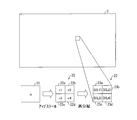
図2は、画像処理装置10の処理内容を説明するための模式図である。この図の符号21は、入力画像(原画像)データとして2K1Kの画像データを示し、符号22は、アップスケール回路11によりアップスケール処理が施された4K2Kのアップスケール後画像データを示し、符号23は、再分配回路12によって輝度が再分配された再分配後画像データを示している。また、ここでは一例として、図2に示すように、入力画像データを構成する複数の画素のうち1画素に着目して説明する。また、この1画素の入力画像データは、n階調に相当するデータであると仮定する。
まず、n階調の画像データ21がアップスケール回路11に入力され、4つの画素(分割画素)に応じてアップスケールされる(アップスケール後画像データ)。ここでは図2に示すように、n階調の画像データ21が、n1階調の画素データ22a,n2階調の画素データ22b,n3階調の画素データ22c,n4階調の画素データ22dにアップスケールされる。
次に、このアップスケール後画像データが再分配回路12に入力されると、再分配回路12が、4つの画素それぞれの輝度値と、各画素で構成される1画素グループの輝度値とを算出する。具体的には、階調から輝度を求める関数をL(K)(cd/m2)とすると、それぞれの画素の輝度値は、L(n1),L(n2),L(n3),L(n4)で表され、1画素グループの輝度値LAは、
LA=(L(n1)+L(n2)+L(n3)+L(n4))/4
で表される。
LA=(L(n1)+L(n2)+L(n3)+L(n4))/4
で表される。
次に、アップスケールする前の入力画像データに対応する輝度値と、アップスケール後画像データの各画素の輝度値との差DLを算出する。各画素に対応する輝度差DLは、アップスケールする前の入力画像データに対応する輝度値をL(M)とすると、
画素23a:DL(n1)=L(n1)―L(M)
画素23b:DL(n2)=L(n2)-L(M)
画素23c:DL(n3)=L(n3)-L(M)
画素23d:DL(n4)=L(n4)-L(M)
で表される。ここで、例えば輝度が、
L(n1)>L(n2)>L(n3)>L(n4)
であると仮定する。
画素23a:DL(n1)=L(n1)―L(M)
画素23b:DL(n2)=L(n2)-L(M)
画素23c:DL(n3)=L(n3)-L(M)
画素23d:DL(n4)=L(n4)-L(M)
で表される。ここで、例えば輝度が、
L(n1)>L(n2)>L(n3)>L(n4)
であると仮定する。
アップスケールする前の入力画像データに対応する輝度値L(M)は、再分配後の各画素に対応する輝度を、LT(n1),LT(n2),LT(n3),LT(n4)とすると、
L(M)=(LT(n1)+LT(n2)+LT(n3)+LT(n4))/4
で表される。
L(M)=(LT(n1)+LT(n2)+LT(n3)+LT(n4))/4
で表される。
また、輝度と画素サイズに応じて決定されるパラメータ(分配比率)をαとすると、再分配後の各画素に対応する輝度LTは、次の関係式を満たす。
LT(n1)-LT(n2)<α1(LA)
LT(n2)-LT(n3)<α2(LA)
LT(n3)-LT(n4)<α3(LA)
α3<α2<α1<α
これにより、各画素の輝度値Lは、
画素23a:L1=LT(n1)+DL(n1)
画素23b:L2=LT(n2)+DL(n2)
画素23c:L3=LT(n3)+DL(n3)
画素23d:L4=LT(n4)+DL(n4)
で表される。
LT(n1)-LT(n2)<α1(LA)
LT(n2)-LT(n3)<α2(LA)
LT(n3)-LT(n4)<α3(LA)
α3<α2<α1<α
これにより、各画素の輝度値Lは、
画素23a:L1=LT(n1)+DL(n1)
画素23b:L2=LT(n2)+DL(n2)
画素23c:L3=LT(n3)+DL(n3)
画素23d:L4=LT(n4)+DL(n4)
で表される。
そして、得られた輝度値Lを、変換関数D(L)により階調値D(L1)~D(L4)に変換する。
画素23a:D(L1)
画素23b:D(L2)
画素23c:D(L3)
画素22d:D(L4)
このようにして得られた階調値を液晶表示パネル2へ出力することにより、アップスケールした画像データを再分配した再分配後画像データを表示させることができる。
画素23a:D(L1)
画素23b:D(L2)
画素23c:D(L3)
画素22d:D(L4)
このようにして得られた階調値を液晶表示パネル2へ出力することにより、アップスケールした画像データを再分配した再分配後画像データを表示させることができる。
なお、上記再分配後の各画素に対応する輝度値LT(n1),LT(n2),LT(n3),LT(n4)は、アップスケール処理部においてアップスケールされた複数の分割画素それぞれの画像データで表される輝度値L(n1),L(n2),L(n3),L(n4)により、一例として、
LT(n1)=L(n1)+β1×(α×(L(n1)―L(M)))
LT(n2)=L(n2)+β2×(α×(L(n2)―L(M)))
LT(n3)=L(n3)+β3×(α×(L(n3)―L(M)))
LT(n4)=L(n4)+β4×(α×(L(n4)―L(M)))
のように決定することができる。ここで、β1、β2、β3、β4は、各分割画素間で輝度差を設けるための画素割合を表すパラメータであり、、β1+β2+β3+β4=4を満たす。ただし、本発明における上記再分配後の各画素に対応する輝度値と、アップスケール処理部においてアップスケールされた複数の分割画素それぞれの画像データで表される輝度値との関係は上記関係式に限定されるものではない。
LT(n1)=L(n1)+β1×(α×(L(n1)―L(M)))
LT(n2)=L(n2)+β2×(α×(L(n2)―L(M)))
LT(n3)=L(n3)+β3×(α×(L(n3)―L(M)))
LT(n4)=L(n4)+β4×(α×(L(n4)―L(M)))
のように決定することができる。ここで、β1、β2、β3、β4は、各分割画素間で輝度差を設けるための画素割合を表すパラメータであり、、β1+β2+β3+β4=4を満たす。ただし、本発明における上記再分配後の各画素に対応する輝度値と、アップスケール処理部においてアップスケールされた複数の分割画素それぞれの画像データで表される輝度値との関係は上記関係式に限定されるものではない。
ここで、具体例を以下に示す。図3は、入力画像データを構成する複数の画素のうち1画素の入力画像データに対してアップスケール処理が実行された様子を示している。ここでは、1画素の入力画像データが、128階調に相当するデータであると仮定する。
まず、元画像データに相当する128階調の画像データがアップスケール回路11に入力され、4つの画素(分割画素)に応じてアップスケールされる(アップスケール後画像データ)。ここでは図3に示すように、128階調の画像データが、128階調の画素データ22a,63階調の画素データ22b,132階調の画素データ22c,78階調の画素データ22dにアップスケールされる。
このアップスケール後画像データが再分配回路12に入力されると、再分配回路12において上記各式の変換処理が実行され、輝度値が再分配される。そして、再分配後の階調値D(L1)~D(L4)は、
画素23a:D(L1)=134
画素23b:D(L2)=44
画素23c:D(L3)=139
画素22d:D(L4)=61
となる。
画素23a:D(L1)=134
画素23b:D(L2)=44
画素23c:D(L3)=139
画素22d:D(L4)=61
となる。
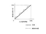
図4は、本実施形態に係る画像処理装置10により得られた再分配後画像データにより表示した場合の輝度特性を示すグラフである。このグラフでは、図9に示すグラフと同様、4つの画素(a~d画素)からなる1画素における、入力信号輝度に対する出力表示輝度を表している。図9のグラフと比較して分かるように、液晶表示パネル2を横斜め60度から見た場合に生じる白浮きを抑えることができる。すなわち、液晶表示パネル2を横斜め60度から見た場合の輝度特性を、液晶表示パネル2を正面から見た場合の輝度特性に近づけることができるため、視野角特性を向上させることができる。
ここで、再分配回路12における変換処理において設定されるパラメータαは、輝度と画素サイズの関数で決められるものである。また、パラメータαは、表示画像として違和感がない程度において、分割画素間の輝度差が大きくなるように設定される。具体例を挙げると、画素サイズが視認距離1.5hにおいて確認できない大きさ(65インチの場合、約0.3mm×0.3mm程度)以上では、分割画素間の輝度差が100cd/m2程度となるように、パラメータαを100cd/m2以下に設定することが好ましい。
このように、本実施形態に係る画像処理装置10では、アップスケールを行った映像信号に、視野角を改善するための再分配処理を行うことにより、高精細な画像を得るとともに視野角を改善することができる。ここで、再分配処理後の他の例を挙げると、例えば、4画素が全て同じデータの場合は、図5のように、1画素に輝度を集中させ198階調と0階調表示とすると、視野角の改善効果が最大となる。
但し、1画素に輝度を集中させてしまうと、画像の精細度が低下してしまう。また、アップスケールをした場合、4つの画素が全て同じ値であるとは限らず、むしろ異なる場合が多い。そのため、アップスケールによる画像データの高精細度を保ちつつ、視野角を改善するためには、例えば画素サイズが0.3mmピッチの場合、再分配後の階調値が0階調~140階調程度であって、分割画素間の輝度差が100cd/m2程度であることが好ましい。
ここで、上記説明では、アップスケールのサイズが4倍(縦横2倍)の構成について説明したが、これに限定されるものではなく、整数倍であれば、上記と同様な効果が得られる。
また、上記説明では、単色の場合を想定しているが、これに限定されるものではなく、1画素がRGBの複数のサブ画素で構成されていてもよく、サブ画素ごとにそれぞれ同様の処理を行うことができる。この場合には、視感度が色(R・G・B)によって異なるため、RGBによってパラメータα(分配比率)を個別に設定することが好ましい。また、RGBで構成されている場合であっても、RGB画素の全てに対して再分配処理を行う必要はなく、RGB画素のうちの1つのサブ画素、例えばB画素のみに対して、再分配処理を行うことも可能である。
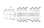
以下では、1画素がRGBのサブ画素に分割されている場合の一例について説明する。図6は、入力画像データを構成する複数の画素のうち、RGBのサブ画素で構成される1画素の入力画像データに対してアップスケール処理が実行された様子を示している。ここでは、1画素の入力画像データが、128階調に相当するR画素データ,192階調に相当するG画素データ,128階調に相当するB画素データであると仮定する。
まず、元画像データである3つのサブ画素の画像データ31がアップスケール回路11(図1参照)に入力され、12個の画素(分割画素)に応じてアップスケールされる(アップスケール後画像データ)。ここでは図6に示すように、128階調のR画像データ31Rが、128階調のR画素データ32Ra,63階調のR画素データ32Rb,132階調のR画素データ32Rc,78階調のR画素データ32Rdにアップスケールされ、192階調のG画像データ31Gが、192階調のG画素データ32Ga,64階調のG画素データ32Gb,192階調のG画素データ32Gc,78階調のG画素データ32Gdにアップスケールされ、128階調のB画像データ31Bが、128階調のB画素データ32Ba,63階調のB画素データ32Bb,132階調のB画素データ32Bc,78階調のB画素データ32Bdにアップスケールされる。
このアップスケール後画像データが再分配回路12(図1参照)に入力されると、再分配回路12において、図7の(a)~(c)に示すように、RGB画素ごとに、上記各式の変換処理が実行され、輝度値が再分配される。そして、再分配後の階調値D(L1)~D(L12)は、
画素33Ra:D(L1)=134
画素33Rb:D(L2)=44
画素33Rc:D(L3)=139
画素33Rd:D(L4)=61
画素33Ga:D(L5)=192
画素33Gb:D(L6)=64
画素33Gc:D(L7)=192
画素33Gd:D(L8)=78
画素33Ba:D(L9)=0
画素33Bb:D(L10)=0
画素33Bc:D(L11)=198
画素33Bd:D(L12)=0
となる。
画素33Ra:D(L1)=134
画素33Rb:D(L2)=44
画素33Rc:D(L3)=139
画素33Rd:D(L4)=61
画素33Ga:D(L5)=192
画素33Gb:D(L6)=64
画素33Gc:D(L7)=192
画素33Gd:D(L8)=78
画素33Ba:D(L9)=0
画素33Bb:D(L10)=0
画素33Bc:D(L11)=198
画素33Bd:D(L12)=0
となる。
このように、1画素がRGBのサブ画素で構成されている場合には、サブ画素ごとに分配比率を設定して個別に再分配処理することができる。そして、サブ画素ごとに輝度への寄与度が異なるため、分割画素間の輝度差が、例えば100cd/m2以上の高い輝度差であっても、1画素あたりの再分配前後の輝度変化を抑えることができる。そのため、このような高輝度差に対しても再分配処理が可能となる。
また、サブ画素ごとに再分配処理ができるため、サブ画素ごとに再分配処理機能をON/OFFする構成とすることも可能である。
具体例を挙げると、例えば、RGBの輝度比は、CIE表色系によると、
L(R画素):L(G画素):L(B画素)=1:4.5907:0.0601
であるため、輝度への寄与度が少ないB画素では、より大きな輝度差をつけて再分配することができる。
L(R画素):L(G画素):L(B画素)=1:4.5907:0.0601
であるため、輝度への寄与度が少ないB画素では、より大きな輝度差をつけて再分配することができる。
これにより、アップスケールした画像データの再分配前後の輝度を変えることなく、表示画像の高精細化および視野角改善の効果をより向上させることができる。
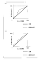
図8は、再分配後画像データにより表示した場合の輝度特性を示すグラフであり、(a)は、輝度差の制限を考慮した場合の輝度特性、すなわちRGBのサブ画素に対して同一の分配比率を設定した場合の輝度特性を示し、(b)は、サブ画素(R・G・B)ごとに個別に分配比率を設定した場合の輝度特性を示している。この図からも分かるように、サブ画素(R・G・B)ごとに個別に分配比率を設定することにより、再分配前後の輝度を変えることなく、表示画像の高精細化および視野角改善の効果をより向上させることができる。
ところで、図1では液晶駆動回路13を1つのブロックとして表記しているが、これに限らず、複数のブロックによって構成されていてもよい。例えば、アップスケール回路11を複数備えるとともに、複数のアップスケール回路11に対応して、再分配回路12および液晶駆動回路13を複数設け、これら各液晶駆動回路によって、液晶表示パネル2における分割領域を駆動するようにしてもよい。1つの液晶駆動回路13で液晶表示パネル2の全体を駆動する場合、各領域の駆動タイミングを容易に一致させることができるので制御性がよいという利点がある一方、入出力ピン数が多くなるので回路サイズ(ICサイズ)が大きくなってしまう。また、液晶駆動回路13を分割領域に応じて複数設ける場合、チップサイズを小さくできるという利点がある(特に本実施形態の場合、各分割領域が2K1Kクラスであるので従来の2K1Kクラスの表示装置に用いられている2Kコントロールチップを使用できるので経済的である)一方、各液晶駆動回路13の同期を保つための調停回路を設ける必要がある。
また、画像処理装置10を構成する各回路(各ブロック)は、CPU等のプロセッサを用いてソフトウェアによって実現されてもよい。すなわち、画像処理装置10は、各機能を実現する制御プログラムの命令を実行するCPU(central processing unit)、上記プログラムを格納したROM(read only memory)、上記プログラムを展開するRAM(random access memory)、上記プログラムおよび各種データを格納するメモリ等の記憶装置(記録媒体)などを備えている構成としてもよい。この場合、本発明の目的は、上述した機能を実現するソフトウェアである画像処理装置10の制御プログラムのプログラムコード(実行形式プログラム、中間コードプログラム、ソースプログラム)をコンピュータで読み取り可能に記録した記録媒体を、画像処理装置10に供給し、そのコンピュータ(またはCPUやMPU)が記録媒体に記録されているプログラムコードを読み出し実行することによって達成される。
上記記録媒体としては、例えば、磁気テープやカセットテープ等のテープ系、フロッピー(登録商標)ディスク/ハードディスク等の磁気ディスクやCD-ROM/MO/MD/DVD/CD-R等の光ディスクを含むディスク系、ICカード(メモリカードを含む)/光カード等のカード系、あるいはマスクROM/EPROM/EEPROM/フラッシュROM等の半導体メモリ系などを用いることができる。
また、画像処理装置10を通信ネットワークと接続可能に構成し、通信ネットワークを介して上記プログラムコードを供給してもよい。この通信ネットワークとしては、特に限定されず、例えば、インターネット、イントラネット、エキストラネット、LAN、ISDN、VAN、CATV通信網、仮想専用網(virtual private network)、電話回線網、移動体通信網、衛星通信網等が利用可能である。また、通信ネットワークを構成する伝送媒体としては、特に限定されず、例えば、IEEE1394、USB、電力線搬送、ケーブルTV回線、電話線、ADSL回線等の有線でも、IrDAやリモコンのような赤外線、Bluetooth(登録商標)、802.11無線、HDR、携帯電話網、衛星回線、地上波デジタル網等の無線でも利用可能である。なお、本発明は、上記プログラムコードが電子的な伝送で具現化された、搬送波に埋め込まれたコンピュータデータ信号の形態でも実現され得る。
また、画像処理装置10の各回路(各ブロック)は、ソフトウェアを用いて実現されるものであってもよく、ハードウェアロジックによって構成されるものであってもよく、処理の一部を行うハードウェアと当該ハードウェアの制御や残余の処理を行うソフトウェアを実行する演算手段とを組み合わせたものであってもよい。
本発明は上述した実施形態に限定されるものではなく、請求項に示した範囲で種々の変更が可能である。すなわち、請求項に示した範囲で適宜変更した技術的手段を組み合わせて得られる実施形態についても本発明の技術的範囲に含まれる。
発明の詳細な説明の項においてなされた具体的な実施形態または実施例は、あくまでも、本発明の技術内容を明らかにするものであって、そのような具体例にのみ限定して狭義に解釈されるべきものではなく、本発明の精神と次に記載する請求の範囲内において、いろいろと変更して実施することができるものである。
本発明は、入力される画像データの解像度を高解像度にアップスケールする画像処理装置および画像処理方法に適用できる。
1 表示装置
2 液晶表示パネル(表示部)
10 画像処理装置
11 アップスケール回路(アップスケール処理部)
12 再分配回路(再分配処理部)
13 液晶駆動回路
31R,31G,31B サブ画素(R画素,G画素,B画素)
2 液晶表示パネル(表示部)
10 画像処理装置
11 アップスケール回路(アップスケール処理部)
12 再分配回路(再分配処理部)
13 液晶駆動回路
31R,31G,31B サブ画素(R画素,G画素,B画素)
Claims (14)
- 入力画像データの解像度を高解像度にアップスケールするためのアップスケール処理部を備えた画像処理装置であって、
入力画像データの1画素に対応する、上記アップスケール処理部においてアップスケールされた複数の分割画素それぞれの階調値を、該複数の分割画素間で再分配する再分配処理部を備えていることを特徴とする画像処理装置。 - 上記再分配処理部は、入力画像データの1画素に対応する上記アップスケール処理部においてアップスケールされた複数の分割画素それぞれの画像データで表される輝度と、該複数の分割画素それぞれの再分配後の画像データで表される輝度とが互いに等しくなるように、アップスケール後の各分割画素の階調値を再分配することを特徴とする請求項1に記載の画像処理装置。
- 上記再分配処理部は、アップスケールする前の入力画像データの各画素における輝度の値と、該画素に対応する複数の分割画素における再分配後の輝度の平均値とが互いに等しくなるように、アップスケール後の各分割画素の階調値を再分配することを特徴とする請求項1に記載の画像処理装置。
- 入力画像データの解像度を高解像度にアップスケールするためのアップスケール処理部を備え、アップスケールされた画像を、1画素がRGBそれぞれに対応するサブ画素に分割されてなる表示部に表示させる画像処理装置であって、
入力画像データの1画素において、上記アップスケール処理部によりアップスケールされた、各サブ画素に対応する複数の分割画素それぞれの階調値を、該複数の分割画素間で再分配する再分配処理部を備えていることを特徴とする画像処理装置。 - 上記再分配処理部は、入力画像データの1画素において、上記アップスケール処理部によりアップスケールされた、各サブ画素に対応する複数の分割画素それぞれの画像データで表される輝度と、該複数の分割画素それぞれの再分配後の画像データで表される輝度とが互いに等しくなるように、アップスケール後の各分割画素の階調値を再分配することを特徴とする請求項4に記載の画像処理装置。
- 上記再分配処理部は、入力画像データの1画素において、サブ画素ごとに設定された分配比率に基づいて、アップスケール後の各分割画素の階調値を再分配することを特徴とする請求項5に記載の画像処理装置。
- 上記再分配処理部は、アップスケールする前の入力画像データの各サブ画素における輝度の値と、該サブ画素に対応する複数の分割画素における再分配後の輝度の平均値とが互いに等しくなるように、アップスケール後の各分割画素の階調値を再分配することを特徴とする請求項4に記載の画像処理装置。
- 請求項1~7の何れか1項に記載の画像処理装置と、
上記画像処理装置によってアップスケールされた画像を表示する表示部とを備えていることを特徴とする表示装置。 - 入力画像データの解像度を高解像度にアップスケールするためのアップスケール処理ステップを含む画像処理方法であって、
入力画像データの1画素に対応する、上記アップスケール処理ステップにおいてアップスケールした複数の分割画素それぞれの階調値を、該複数の分割画素間で再分配する再分配処理ステップを含むことを特徴とする画像処理方法。 - 上記再分配処理ステップでは、入力画像データの1画素に対応する上記アップスケール処理ステップにおいてアップスケールした複数の分割画素それぞれの画像データで表される輝度と、該複数の分割画素それぞれの再分配後の画像データで表される輝度とが互いに等しくなるように、アップスケール後の各分割画素の階調値を再分配することを特徴とする請求項9に記載の画像処理方法。
- 入力画像データの解像度を高解像度にアップスケールするためのアップスケール処理ステップを含み、アップスケールした画像を、1画素がRGBそれぞれに対応するサブ画素に分割されてなる表示部に表示させるための画像処理方法であって、
入力画像データの1画素において、上記アップスケール処理ステップによりアップスケールした、各サブ画素に対応する複数の分割画素それぞれの階調値を、該複数の分割画素間で再分配する再分配処理ステップを含むことを特徴とする画像処理方法。 - 上記再分配処理ステップでは、入力画像データの1画素において、上記アップスケール処理ステップにおいてアップスケールした、各サブ画素に対応する複数の分割画素それぞれの画像データで表される輝度と、該複数の分割画素それぞれの再分配後の画像データで表される輝度とが互いに等しくなるように、アップスケール後の各分割画素の階調値を再分配することを特徴とする請求項11に記載の画像処理方法。
- コンピュータを請求項1~7の何れか1項に記載の画像処理装置として動作させるためのプログラムであって、上記コンピュータを上記画像処理装置の上記各部として機能させるプログラム。
- 請求項13に記載のプログラムが記録されたコンピュータ読み取り可能な記録媒体。
Priority Applications (2)
| Application Number | Priority Date | Filing Date | Title |
|---|---|---|---|
| CN2009801234901A CN102067204A (zh) | 2008-08-06 | 2009-06-02 | 图像处理装置、显示装置、图像处理方法、程序和记录介质 |
| US12/737,181 US20110081080A1 (en) | 2008-08-06 | 2009-06-02 | Image processing device, display device, image processing method, program and recording medium |
Applications Claiming Priority (2)
| Application Number | Priority Date | Filing Date | Title |
|---|---|---|---|
| JP2008-203541 | 2008-08-06 | ||
| JP2008203541 | 2008-08-06 |
Publications (1)
| Publication Number | Publication Date |
|---|---|
| WO2010016319A1 true WO2010016319A1 (ja) | 2010-02-11 |
Family
ID=41663544
Family Applications (1)
| Application Number | Title | Priority Date | Filing Date |
|---|---|---|---|
| PCT/JP2009/060087 Ceased WO2010016319A1 (ja) | 2008-08-06 | 2009-06-02 | 画像処理装置、表示装置、画像処理方法、プログラム、及び、記録媒体 |
Country Status (3)
| Country | Link |
|---|---|
| US (1) | US20110081080A1 (ja) |
| CN (1) | CN102067204A (ja) |
| WO (1) | WO2010016319A1 (ja) |
Families Citing this family (8)
| Publication number | Priority date | Publication date | Assignee | Title |
|---|---|---|---|---|
| CN102368375B (zh) * | 2011-09-16 | 2015-04-08 | 广东威创视讯科技股份有限公司 | 点阵显示屏分辨率倍增的方法、装置及点阵显示屏系统 |
| US10878544B2 (en) * | 2011-11-03 | 2020-12-29 | Koninklijke Philips N.V. | Image data processing |
| CN102903320B (zh) * | 2012-08-17 | 2015-02-18 | 深圳市华星光电技术有限公司 | 4k2k分辨率放大方法及应用该方法的4k2k分辨率放大系统 |
| US10147350B2 (en) * | 2013-07-26 | 2018-12-04 | Darwin Hu | Method and apparatus for increasing perceived display resolutions from an input image |
| US10546521B2 (en) * | 2017-05-16 | 2020-01-28 | Darwin Hu | Resolutions by modulating both amplitude and phase in spatial light modulators |
| CN110718181B (zh) * | 2018-07-12 | 2021-09-21 | 杭州海康威视数字技术股份有限公司 | 信号源备份方法、装置、系统及led控制器 |
| TWI783282B (zh) * | 2020-10-23 | 2022-11-11 | 欣興電子股份有限公司 | 具有顯示功能的後視鏡 |
| CN114506276A (zh) * | 2020-10-23 | 2022-05-17 | 欣兴电子股份有限公司 | 具有显示功能的后视镜 |
Citations (2)
| Publication number | Priority date | Publication date | Assignee | Title |
|---|---|---|---|---|
| JP2004085608A (ja) * | 2002-08-22 | 2004-03-18 | Seiko Epson Corp | 画像表示装置、画像表示方法及び画像表示プログラム |
| JP2004117752A (ja) * | 2002-09-25 | 2004-04-15 | Sharp Corp | 表示装置 |
-
2009
- 2009-06-02 CN CN2009801234901A patent/CN102067204A/zh active Pending
- 2009-06-02 US US12/737,181 patent/US20110081080A1/en not_active Abandoned
- 2009-06-02 WO PCT/JP2009/060087 patent/WO2010016319A1/ja not_active Ceased
Patent Citations (2)
| Publication number | Priority date | Publication date | Assignee | Title |
|---|---|---|---|---|
| JP2004085608A (ja) * | 2002-08-22 | 2004-03-18 | Seiko Epson Corp | 画像表示装置、画像表示方法及び画像表示プログラム |
| JP2004117752A (ja) * | 2002-09-25 | 2004-04-15 | Sharp Corp | 表示装置 |
Also Published As
| Publication number | Publication date |
|---|---|
| US20110081080A1 (en) | 2011-04-07 |
| CN102067204A (zh) | 2011-05-18 |
Similar Documents
| Publication | Publication Date | Title |
|---|---|---|
| CN106298851B (zh) | 一种像素结构、显示面板及其驱动方法 | |
| CN107863081B (zh) | 多基色转换方法及其转换器、显示控制方法、显示装置 | |
| KR102023184B1 (ko) | 표시장치, 데이터 처리장치 및 그 방법 | |
| JP5227018B2 (ja) | 非ストライプディスプレイシステムにおける画像データのサブピクセルレンダリングを改良するためのシステムおよび方法 | |
| WO2010016319A1 (ja) | 画像処理装置、表示装置、画像処理方法、プログラム、及び、記録媒体 | |
| CN101523478B (zh) | 显示装置和信号转换装置 | |
| JP2010020241A (ja) | 表示装置、表示装置の駆動方法、駆動用集積回路、駆動用集積回路による駆動方法及び信号処理方法 | |
| CN106560880B (zh) | 显示装置和该显示装置的图像渲染方法 | |
| KR101686236B1 (ko) | 대칭적 배열을 가진 rgbgr 디스플레이 장치 | |
| CN108428435B (zh) | 一种子像素渲染的验证显示方法 | |
| WO2016192367A1 (zh) | 阵列基板及显示装置 | |
| CN109461400B (zh) | 用于rgb到rgbw图像转换的子像素渲染方法及装置 | |
| US8094172B2 (en) | Image display device and liquid crystal television having distributed subframe image data to a plurality of pixels | |
| KR20160048312A (ko) | 입력 영상의 업 스케일링을 위한 데이터 변환부와 데이터 변환 방법 | |
| JP2002318561A (ja) | 表示装置及び表示方法 | |
| CN104464684B (zh) | 对显示器的画面进行渲染的方法 | |
| CN101292279B (zh) | 用于图像处理的改进的存储器结构 | |
| TWI575506B (zh) | 顯示控制單元、顯示裝置以及顯示控制方法 | |
| CN103295545B (zh) | 图像显示装置及其驱动方法、灰度转换装置 | |
| KR20160031650A (ko) | 표시장치 및 표시패널 | |
| TWI527013B (zh) | 顯示面板與資料轉換方法 | |
| JP2007017615A (ja) | 画像処理装置,画像処理方法及びプログラム | |
| WO2010116432A1 (ja) | 画像処理装置、表示装置、画像処理方法、プログラム、及び、記録媒体 | |
| US20090278855A1 (en) | Memory structures for image processing | |
| TWI856806B (zh) | 屏下指紋識別區顯示方法、顯示驅動電路及資訊處理裝置 |
Legal Events
| Date | Code | Title | Description |
|---|---|---|---|
| WWE | Wipo information: entry into national phase |
Ref document number: 200980123490.1 Country of ref document: CN |
|
| 121 | Ep: the epo has been informed by wipo that ep was designated in this application |
Ref document number: 09804806 Country of ref document: EP Kind code of ref document: A1 |
|
| NENP | Non-entry into the national phase |
Ref country code: DE |
|
| NENP | Non-entry into the national phase |
Ref country code: JP |
|
| 122 | Ep: pct application non-entry in european phase |
Ref document number: 09804806 Country of ref document: EP Kind code of ref document: A1 |