WO2010013293A1 - プラズマ装置および結晶製造方法 - Google Patents
プラズマ装置および結晶製造方法 Download PDFInfo
- Publication number
- WO2010013293A1 WO2010013293A1 PCT/JP2008/002068 JP2008002068W WO2010013293A1 WO 2010013293 A1 WO2010013293 A1 WO 2010013293A1 JP 2008002068 W JP2008002068 W JP 2008002068W WO 2010013293 A1 WO2010013293 A1 WO 2010013293A1
- Authority
- WO
- WIPO (PCT)
- Prior art keywords
- cathode
- gas
- sample
- anode
- plasma jet
- Prior art date
- Legal status (The legal status is an assumption and is not a legal conclusion. Google has not performed a legal analysis and makes no representation as to the accuracy of the status listed.)
- Ceased
Links
Images



Classifications
-
- C—CHEMISTRY; METALLURGY
- C23—COATING METALLIC MATERIAL; COATING MATERIAL WITH METALLIC MATERIAL; CHEMICAL SURFACE TREATMENT; DIFFUSION TREATMENT OF METALLIC MATERIAL; COATING BY VACUUM EVAPORATION, BY SPUTTERING, BY ION IMPLANTATION OR BY CHEMICAL VAPOUR DEPOSITION, IN GENERAL; INHIBITING CORROSION OF METALLIC MATERIAL OR INCRUSTATION IN GENERAL
- C23C—COATING METALLIC MATERIAL; COATING MATERIAL WITH METALLIC MATERIAL; SURFACE TREATMENT OF METALLIC MATERIAL BY DIFFUSION INTO THE SURFACE, BY CHEMICAL CONVERSION OR SUBSTITUTION; COATING BY VACUUM EVAPORATION, BY SPUTTERING, BY ION IMPLANTATION OR BY CHEMICAL VAPOUR DEPOSITION, IN GENERAL
- C23C16/00—Chemical coating by decomposition of gaseous compounds, without leaving reaction products of surface material in the coating, i.e. chemical vapour deposition [CVD] processes
- C23C16/22—Chemical coating by decomposition of gaseous compounds, without leaving reaction products of surface material in the coating, i.e. chemical vapour deposition [CVD] processes characterised by the deposition of inorganic material, other than metallic material
- C23C16/30—Deposition of compounds, mixtures or solid solutions, e.g. borides, carbides, nitrides
- C23C16/308—Oxynitrides
-
- C—CHEMISTRY; METALLURGY
- C23—COATING METALLIC MATERIAL; COATING MATERIAL WITH METALLIC MATERIAL; CHEMICAL SURFACE TREATMENT; DIFFUSION TREATMENT OF METALLIC MATERIAL; COATING BY VACUUM EVAPORATION, BY SPUTTERING, BY ION IMPLANTATION OR BY CHEMICAL VAPOUR DEPOSITION, IN GENERAL; INHIBITING CORROSION OF METALLIC MATERIAL OR INCRUSTATION IN GENERAL
- C23C—COATING METALLIC MATERIAL; COATING MATERIAL WITH METALLIC MATERIAL; SURFACE TREATMENT OF METALLIC MATERIAL BY DIFFUSION INTO THE SURFACE, BY CHEMICAL CONVERSION OR SUBSTITUTION; COATING BY VACUUM EVAPORATION, BY SPUTTERING, BY ION IMPLANTATION OR BY CHEMICAL VAPOUR DEPOSITION, IN GENERAL
- C23C16/00—Chemical coating by decomposition of gaseous compounds, without leaving reaction products of surface material in the coating, i.e. chemical vapour deposition [CVD] processes
- C23C16/44—Chemical coating by decomposition of gaseous compounds, without leaving reaction products of surface material in the coating, i.e. chemical vapour deposition [CVD] processes characterised by the method of coating
- C23C16/453—Chemical coating by decomposition of gaseous compounds, without leaving reaction products of surface material in the coating, i.e. chemical vapour deposition [CVD] processes characterised by the method of coating passing the reaction gases through burners or torches, e.g. atmospheric pressure CVD
Definitions
- the present invention relates to a plasma apparatus and a crystal manufacturing method, and more particularly to a plasma apparatus and a crystal manufacturing method using a direct current arc discharge.
- the plasma jet film forming apparatus includes a plasma torch, a vacuum chamber, a substrate holder, and a powder supply unit.
- the substrate holder is disposed opposite to the plasma torch in the vacuum chamber and holds the substrate.
- the powder supply unit supplies carbon particles as a raw material for the carbon protective film to the plasma torch.
- an arc discharge is generated in the plasma torch, and carbon particles are supplied together with a carrier gas into the formed plasma.
- the carbon particles are converted into carbon ions and emitted as a plasma jet to the substrate, and a carbon protective film is deposited on the substrate.
- the conventional plasma jet film forming apparatus ionizes the raw material of the carbon protective film deposited on the substrate in the plasma to form the carbon protective film on the substrate, the thin film formed on the substrate is not formed. It is difficult to produce crystals by using them.
- the plasma device includes a cathode, an anode, a sample holder, and a DC power source.
- the anode is disposed around the cathode.
- the sample holder holds a sample arranged to face the tip of the cathode.
- the DC power source applies a DC voltage between the cathode and the anode, and irradiates the sample with a thermal plasma jet from the tip of the cathode.
- the plasma apparatus may further include a first supply and a second supply.
- the first supply pipe supplies an inert gas between the cathode and the anode.
- the second supply tube supplies a gas serving as an oxygen source and / or a nitrogen source from around the thermal plasma jet emitted from the tip of the cathode.
- the cathode may be made of any of tungsten, hafnium and zirconium.
- the first supply pipe supplies argon gas between the cathode and the anode.
- the second supply pipe supplies nitrogen gas and / or oxygen gas from around the thermal plasma jet.
- the plasma device may further include a moving device.
- the moving device moves the sample in a plane direction of the sample at a desired speed.
- the sample may be composed of a substrate and amorphous silicon formed on the substrate.
- the first supply pipe supplies argon gas between the cathode and the anode.
- the second supply pipe supplies nitrogen gas and / or oxygen gas from around the thermal plasma jet.
- the crystal manufacturing method includes a first step of arranging a sample on a sample holder arranged to face the cathode and the anode, a second step of supplying an inert gas between the cathode and the anode, A third step of supplying a gas serving as an oxygen source and / or a nitrogen source from the periphery of the thermal plasma jet emitted from the tip of the cathode, closer to the sample holder than the tip of the cathode, and between the cathode and the anode And a fourth step of applying a direct current voltage to the sample and irradiating the sample with a thermal plasma jet from the tip of the cathode.
- the gas serving as the oxygen source and / or nitrogen source may be supplied from a position different from the inert gas in the third step.
- the cathode may be made of any of tungsten, hafnium and zirconium.
- argon gas is supplied as an inert gas.
- oxygen gas and / or nitrogen gas is supplied as a gas that becomes an oxygen source and / or a nitrogen source.
- the crystal manufacturing method may further include a fifth step of moving the sample in the plane direction of the sample at a desired speed.
- a direct current voltage is supplied between the cathode and the anode to generate a thermal plasma jet, and the generated thermal plasma jet is irradiated to the amorphous material to produce a crystalline material.
- crystals can be manufactured using an amorphous thin film formed on a substrate.
- FIG. 3 is a first process diagram for explaining a manufacturing method of a TFT using the plasma device shown in FIG. 1.
- FIG. 4 is a second process diagram for explaining a method for manufacturing a TFT using the plasma apparatus shown in FIG. 1.
- FIG. 4 is a third process diagram for explaining a method for manufacturing a TFT using the plasma apparatus shown in FIG. 1.
- FIG. 6 is a fourth process diagram for explaining the manufacturing method of the TFT using the plasma device shown in FIG. 1.
- FIG. 1 is a schematic diagram showing a configuration of a plasma apparatus according to an embodiment of the present invention.
- a plasma apparatus 10 according to an embodiment of the present invention includes a reaction vessel 1, a cathode 2, an anode 3, an insulating member 4, pipes 5 and 6, a sample holder 7, and a gas cylinder 8. , 9, 11, valves 12, 13, DC power supply 14, and moving device 15.
- the reaction vessel 1 has a hollow cylindrical shape.
- the cathode 2 is made of tungsten (W) containing 3% LaO 2 .
- the cathode 2 has a substantially cylindrical shape with a diameter of 5 mm and has one end that is sharp. Further, the other end of the cathode 2 penetrates the insulating member 4 and the reaction vessel 1, is disposed outside the reaction vessel 1, and is fixed to the insulating member 4.
- the anode 3 is arranged around the cathode 2 so as to form a space SP between the cathode 2 and fixed to the insulating member 4.
- the anode 3 has a hole 31 through which the thermal plasma jet passes on the sample holder 7 side.
- the insulating member 4 is fixed to the ceiling of the reaction vessel 1.
- the pipe 5 penetrates the anode 3 so that one end is in contact with the space SP, and the other end is connected to the gas cylinder 8. In this case, the pipe 5 penetrates the anode 3 at a position of 1 to 2 cm from the insulating member 4.
- the pipe 6 passes through the anode 3 so that one end thereof is in contact with the hole 31, and the other end is connected to the gas cylinders 9 and 11 via valves 12 and 13, respectively. In this case, the pipe 6 penetrates the anode 3 at a position 4 to 5 cm from the pipe 5.
- the sample holder 7 is disposed to face the cathode 2 and the anode 3.
- the gas cylinder 8 is connected to the other end of the pipe 5 and holds argon (Ar) gas.
- the gas cylinder 9 is connected to the other end of the pipe 6 and holds nitrogen (N 2 ) gas.
- the gas cylinder 11 is connected to the other end of the pipe 6 and holds oxygen (O 2 ) gas.
- the valve 12 is arranged in the pipe 6 in the vicinity of the gas cylinder 9 on the other end side of the pipe 6.
- the valve 13 is disposed in the pipe 6 in the vicinity of the gas cylinder 11 on the other end side of the pipe 6.
- the sample holder 7 holds the sample 20.
- the gas cylinder 8 supplies Ar gas to the space SP via the pipe 5.
- the gas cylinder 9 supplies N 2 gas to the hole 31 through the valve 12 and the pipe 6.
- the gas cylinder 11 supplies O 2 gas to the hole 31 through the valve 13 and the pipe 6.
- the DC power supply 14 includes a DC voltage source 141 and an ammeter 142.
- the DC power supply 14 applies a DC voltage between the cathode 2 and the anode 3 so that a desired current flows.
- the moving device 15 moves the sample holder 7 in the direction DR1 at a constant speed.
- FIG. 2 is a diagram for explaining an example of manufacturing a crystal in the plasma apparatus 10 shown in FIG.
- crystalline silicon c-Si
- sample 20 made of substrate / amorphous silicon a-Si
- a-Si is produced by plasma CVD (Chemical Vapor Deposition), for example, and the film thickness is 50 nm.
- the gas cylinder 8 supplies Ar gas to the space SP at a flow rate of 9.8 liters / minute, the gas cylinder 9 supplies N 2 gas to the hole 31 at a flow rate of 2 liters / minute, and the gas cylinder 11 has 2 O 2 gas is supplied to the hole 31 at a flow rate of 1 liter / min.
- the DC power supply 14 applies a DC voltage of 13 to 14 V between the cathode 2 and the anode 3 so that the DC current becomes 150A.
- the cathode 2 emits the thermal plasma jet 40 and irradiates the sample 20 through the hole 31 with the emitted thermal plasma jet 40.
- the moving device 15 moves the sample holder 7 in the direction of the arrow 32 at a speed of 1 m / s.
- the portion irradiated with the thermal plasma jet 40 is heated to 1200 ° C. in 2 to 3 msec, c-Si 22, a silicon oxygen nitrogen film (SiO x N (4 / 3-2x / 3) film, 0 ⁇ X ⁇ 2) 23.
- the c-Si 22 has a thickness of 40 nm
- the SiO x N (4 / 3-2x / 3) film 23 has a thickness of 28 nm.
- W constituting the cathode 2 dissolves when Ar gas and O 2 gas are present.
- Ar gas and O 2 gas are supplied from different positions through the pipes 5 and 6. Therefore, in the plasma apparatus 10, it is possible to prevent the cathode 2 from melting.
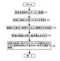
- FIG. 3 is a flowchart for explaining the crystal manufacturing method according to the present invention. Referring to FIG. 3, when a series of operations is started, sample 20 is placed on sample holder 7 (step S1).
- the gas cylinder 8 supplies Ar gas to the space SP between the cathode 2 and the anode 3 via the pipe 5 (step S2).
- the gas cylinder 9 supplies N 2 gas to the hole 31 portion of the anode 3 via the pipe 6, and the gas cylinder 11 supplies O 2 gas to the hole 31 portion of the anode 3 via the pipe 6 ( Step S3).
- the DC power source 14 applies a DC voltage between the cathode 2 and the anode 3 (step S4).
- a direct-current arc discharge is generated at the hole 31, and the cathode 2 irradiates the sample 20 with the thermal plasma jet 40 from its tip.
- the moving device 15 moves the sample 20 at a desired speed in the plane direction of the sample 20 so that the entire surface of the sample 20 is irradiated with the thermal plasma jet 40 (step S5).
- the c-Si 22 and the SiO x N (4 / 3-2x / 3) film 23 are formed on the entire surface of the sample 20, and the series of operations is completed.
- the sample 20 is irradiated with the thermal plasma jet 40 to produce the c-Si 22 and the SiO x N (4 / 3-2x / 3) film 23 from a-Si.
- a crystal can be produced on the substrate 21 using a thin film (a-Si film) formed on the substrate 21.
- TFT Thin Film Transistor
- 4 to 7 are first to fourth process diagrams for explaining a method of manufacturing a TFT using the plasma apparatus 10 shown in FIG.
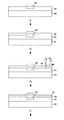
- an SiO 2 film 51 is produced on the glass substrate 50 by plasma CVD (see step (a) in FIG. 4).
- silane (SiH 4 ) gas and oxygen (O 2 ) gas are used as source gases.
- a resist is applied to the entire surface of the SiO 2 film 51, and the applied resist is patterned using photolithography to form a resist pattern 52 on the surface of the SiO 2 film 51 (see step (b) in FIG. 4). ).
- a part of the SiO 2 film 51 is etched to a predetermined depth using the resist pattern 52 as a mask to form a recess 53 (see step (c) in FIG. 4).
- aluminum 54 is deposited on the recess 53 (see step (d) in FIG. 4), and the resist pattern 52 is removed. Thereby, the gate electrode 60 is formed (see step (e) in FIG. 4).
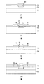
- a SiO 2 film is deposited by plasma CVD so as to cover gate electrode 60.
- the SiO 2 film 55 is formed so as to surround the gate electrode 60 (see step (f) in FIG. 5).
- a p + type a-Si film 56 having a thickness of 50 nm is formed on the entire surface of the SiO 2 film 55 by plasma CVD (see step (g) in FIG. 5).
- diborane (B 2 H 6 ) gas and SiH 4 gas are used as source gases.
- the sample is placed on the sample holder 7 of the plasma apparatus 10, and the thermal plasma jet 40 is moved to the p + type a-Si film 56 while moving the sample in the direction of the arrow 57 by the moving device 15 according to the flowchart shown in FIG. irradiated (FIG. 5 step (h) refer), p + -type a-Si film 56 from the p + -type c-Si58 and SiO x N (4 / 3-2x / 3) to prepare a membrane 59 (FIG. Step 5 (i)).
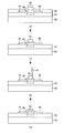
- SiO x N (4 / 3-2x / 3) film 59 is removed by hydrofluoric acid (HF) (see step (j) in FIG. 6).
- a resist is applied to the entire surface of the p + -type c-Si 58, and the applied resist is patterned using photolithography to form a resist pattern 61 on the surface of the p + -type c-Si 58 (step of FIG. 6). (See (k)).
- the p + type c-Si 58 is etched using the resist pattern 61 as a mask, and the resist pattern 61 is removed.
- a source 70 and a drain 80 made of a p-type region are formed on the SiO 2 film 55 (see step (l) in FIG. 6).
- an a-Si film 62 is formed on the entire surface of the sample by plasma CVD (see step (m) in FIG. 6).
- a resist is applied to the entire surface of a-Si film 62, and the applied resist is patterned using photolithography to form resist pattern 63 as a-Si film 62. (See step (n) in FIG. 7).
- a-Si film 62 is etched using the resist pattern 63 as a mask, and the resist pattern 63 is removed. As a result, an a-Si film 64 is formed on the gate electrode 60 (see step (o) in FIG. 7).
- the sample is placed on the sample holder 7 of the plasma apparatus 10, and the a-Si film 64 is irradiated with the thermal plasma jet 40 according to the flowchart shown in FIG. 3 (see step (p) in FIG. 7).
- a c-Si and SiO x N (4 / 3-2x / 3) film are formed from the film 64.
- the fabricated SiO x N (4 / 3-2x / 3) film is etched with HF, and a channel layer 90 made of c-Si is formed between the source 70 and the drain 80, and is formed on the glass substrate 50.
- a TFT is manufactured (see step (q) in FIG. 7).
- a method for manufacturing a TFT having a source 70 and a drain 80 made of a p-type semiconductor has been described, but a TFT having a source 70 and a drain 80 made of an n-type semiconductor can also be made.
- a TFT having a source 70 and a drain 80 made of an n-type semiconductor can also be made.
- an n + type a-Si film is formed on the SiO 2 film 55 by plasma CVD using phosphine (PH 3 ) gas and SiH 4 gas as source gases.
- a TFT may be manufactured using a plastic film substrate.
- the cathode 2 is made of tungsten.
- the present invention is not limited to this, and the cathode 2 may be made of hafnium or zirconium.
- the cathode 2 is preferably made of hafnium.
- both the O 2 gas and the N 2 gas are supplied to the hole 31, but the present invention is not limited to this, and either one of the O 2 gas and the N 2 gas may be supplied to the hole 31. .
- SiO y (0 ⁇ y ⁇ 2) is formed on the c-Si
- SiN on the c-Si z (0 ⁇ z ⁇ 1.3) is formed.
- Ar gas is supplied to the space SP between the cathode 2 and the anode 3.
- the present invention is not limited to this, and helium (He) gas is supplied to the space SP between the cathode 2 and the anode 3.
- helium (He) gas is supplied to the space SP between the cathode 2 and the anode 3.
- an inert gas may be supplied to the space SP between the cathode 2 and the anode 3.
- c-Si is produced from an a-Si film by irradiation with a thermal plasma jet.
- c-Ge may be produced from an a-Ge film by irradiation with a thermal plasma jet.
- a crystalline material may be produced from an amorphous material by irradiation with a thermal plasma jet.
- the present invention is applied to a plasma apparatus capable of producing crystals using a thin film formed on a substrate.
- the present invention is also applied to a crystal manufacturing method capable of manufacturing a crystal using a thin film formed on a substrate.
Landscapes
- Chemical & Material Sciences (AREA)
- Engineering & Computer Science (AREA)
- General Chemical & Material Sciences (AREA)
- Chemical Kinetics & Catalysis (AREA)
- Materials Engineering (AREA)
- Mechanical Engineering (AREA)
- Metallurgy (AREA)
- Organic Chemistry (AREA)
- Inorganic Chemistry (AREA)
- Physics & Mathematics (AREA)
- Plasma & Fusion (AREA)
- Chemical Vapour Deposition (AREA)
Abstract
ガスボンベ(8)は、Arガスを陰極(2)と陽極(3)との間の空間SPに供給し、ガスボンベ(9),(11)は、それぞれ、N2ガスおよびO2ガスを孔(31)へ供給する。直流電源(15)は、150Aの直流電流が流れるように13~14Vの直流電圧を陰極(2)と陽極(3)との間に印加する。その結果、陰極(2)は、熱プラズマジェットを先端部から出射し、熱プラズマジェットを試料(20)に照射する。
Description
この発明は、プラズマ装置および結晶製造方法に関し、特に、直流アーク放電を用いたプラズマ装置および結晶製造方法に関するものである。
従来、アーク放電を用いたプラズマジェット成膜装置が知られている(特開2004-300486)。
このプラズマジェット成膜装置は、プラズマトーチと、真空チャンバと、基板保持台と、粉体供給部とを備える。基板保持台は、真空チャンバ内において、プラズマトーチに対向して配置され、基板を保持する。粉体供給部は、カーボン保護膜の原料となるカーボン粒子をプラズマトーチに供給する。
プラズマジェット成膜装置においては、プラズマトーチにアーク放電を生じさせ、形成されたプラズマ中にキャリアガスと共にカーボン粒子を供給する。そして、プラズマジェット成膜装置においては、カーボン粒子をカーボンイオンに変換してプラズマジェットとして基板に放射し、カーボン保護膜を基板上に堆積させる。
しかし、従来のプラズマジェット成膜装置は、基板上に堆積させるカーボン保護膜の原料をプラズマ中でイオン化してカーボン保護膜を基板上に形成するものであるため、基板上に形成された薄膜を用いて結晶を作製することは困難である。
そこで、基板上に形成された非晶質薄膜を用いて結晶を製造可能なプラズマ装置を提供することが望まれる。
また、基板上に形成された非晶質薄膜を用いて結晶を製造可能な結晶製造方法を提供することが望まれる。
プラズマ装置は、陰極と、陽極と、試料ホルダーと、直流電源とを備える。陽極は、陰極の周囲に配置される。試料ホルダーは、陰極の先端部に対向して配置された試料を保持する。直流電源は、陰極と陽極との間に直流電圧を印加し、陰極の先端部から熱プラズマジェットを試料に照射させる。
プラズマ装置は、第1および第2の供給間をさらに備えてもよい。第1の供給管は、陰極と陽極との間に不活性ガスを供給する。第2の供給管は、陰極の先端部から出射された熱プラズマジェットの周囲から酸素源および/または窒素源となるガスを供給する。
陰極は、タングステン、ハフニウムおよびジルコニウムのいずれかからなってもよい。第1の供給管は、アルゴンガスを陰極と陽極との間に供給する。第2の供給管は、熱プラズマジェットの周囲から窒素ガスおよび/または酸素ガスを供給する。
プラズマ装置は、移動装置をさらに備えてもよい。移動装置は、試料を試料の平面方向へ所望の速度で移動させる。
試料は、基板と、基板上に形成された非晶質シリコンとからなってもよい。第1の供給管は、アルゴンガスを陰極と陽極との間に供給する。第2の供給管は、熱プラズマジェットの周囲から窒素ガスおよび/または酸素ガスを供給する。
また、結晶製造方法は、陰極および陽極に対向して配置された試料ホルダー上に試料を配置する第1のステップと、陰極と陽極との間に不活性ガスを供給する第2のステップと、陰極の先端部よりも試料ホルダー側において、陰極の先端部から出射される熱プラズマジェットの周囲から酸素源および/または窒素源となるガスを供給する第3のステップと、陰極と陽極との間に直流電圧を印加し、陰極の先端部から熱プラズマジェットを試料に照射する第4のステップとを備える。
酸素源および/または窒素源となるガスは、第3のステップにおいて、不活性ガスと異なる位置から供給されてもよい。
陰極は、タングステン、ハフニウムおよびジルコニウムのいずれかからなってもよい。第2のステップにおいて、アルゴンガスが不活性ガスとして供給される。第3のステップにおいて、酸素ガスおよび/または窒素ガスが酸素源および/または窒素源となるガスとして供給される。
結晶製造方法は、試料を試料の平面方向へ所望の速度で移動させる第5のステップをさらに備えてもよい。
陰極と陽極との間に直流電圧を供給して熱プラズマジェットを発生し、その発生した熱プラズマジェットを非晶質材料に照射して結晶材料を製造する。
したがって、基板上に形成された非晶質薄膜を用いて結晶を製造できる。
本発明の実施の形態について図面を参照しながら詳細に説明する。なお、図中同一または相当部分には同一符号を付してその説明は繰返さない。
図1は、この発明の実施の形態によるプラズマ装置の構成を示す概略図である。図1を参照して、この発明の実施の形態によるプラズマ装置10は、反応容器1と、陰極2と、陽極3と、絶縁部材4と、配管5,6と、試料ホルダー7と、ガスボンベ8,9,11と、バルブ12,13と、直流電源14と、移動装置15とを備える。
反応容器1は、中空の円柱形状からなる。陰極2は、3%のLaO2を含むタングステン(W)からなる。そして、陰極2は、直径5mmの略円柱形状を有し、一方端が尖っている。また、陰極2は、他方端が絶縁部材4および反応容器1を貫通し、反応容器1の外部に配置されるとともに、絶縁部材4に固定される。
陽極3は、陰極2との間に空間SPを形成するように陰極2の周囲に配置され、絶縁部材4に固定される。そして、陽極3は、試料ホルダー7側に熱プラズマジェットが通過するための孔31を有する。
絶縁部材4は、反応容器1の天井に固定される。配管5は、一方端が空間SPに接するように陽極3を貫通し、他方端がガスボンベ8に連結される。この場合、配管5は、絶縁部材4から1~2cmの位置で陽極3を貫通する。
配管6は、一方端が孔31に接するように陽極3を貫通し、他方端がバルブ12,13をそれぞれ介してガスボンベ9,11に連結される。この場合、配管6は、配管5から4~5cmの位置で陽極3を貫通する。
試料ホルダー7は、陰極2および陽極3に対向して配置される。ガスボンベ8は、配管5の他方端に連結され、アルゴン(Ar)ガスを保持する。ガスボンベ9は、配管6の他方端に連結され、窒素(N2)ガスを保持する。ガスボンベ11は、配管6の他方端に連結され、酸素(O2)ガスを保持する。
バルブ12は、配管6の他方端側において、ガスボンベ9に近接して配管6中に配置される。バルブ13は、配管6の他方端側において、ガスボンベ11に近接して配管6中に配置される。
試料ホルダー7は、試料20を保持する。ガスボンベ8は、Arガスを配管5を介して空間SPに供給する。ガスボンベ9は、N2ガスをバルブ12および配管6を介して孔31の部分へ供給する。ガスボンベ11は、O2ガスをバルブ13および配管6を介して孔31の部分へ供給する。
直流電源14は、直流電圧源141と、電流計142とを含む。そして、直流電源14は、所望の電流が流れるように、陰極2と陽極3との間に直流電圧を印加する。
移動装置15は、試料ホルダー7を一定速度で方向DR1へ移動させる。
図2は、図1に示すプラズマ装置10において結晶を製造する例を説明するための図である。図2を参照して、基板21上に結晶シリコン(c-Si)を作製する場合、大気圧下で基板/アモルファスシリコン(a-Si)からなる試料20が試料ホルダー7上に配置される。そして、a-Siは、たとえば、プラズマCVD(Chemical Vapour Deposition)によって作製され、その膜厚は、50nmである。
ガスボンベ8は、9.8リットル/分の流量でArガスを空間SPへ供給し、ガスボンベ9は、2リットル/分の流量でN2ガスを孔31の部分へ供給し、ガスボンベ11は、2リットル/分の流量でO2ガスを孔31の部分へ供給する。
また、直流電源14は、直流電流が150Aになるように、陰極2と陽極3との間に13~14Vの直流電圧を印加する。
そうすると、陰極2は、熱プラズマジェット40を出射し、その出射した熱プラズマジェット40を孔31を介して試料20に照射する。
また、移動装置15は、1m/sの速度で矢印32の方向へ試料ホルダー7を移動させる。
その結果、熱プラズマジェット40が照射された部分は、2~3msecで1200℃まで昇温され、c-Si22と、シリコン酸素窒素膜(SiOxN(4/3-2x/3)膜,0<x<2)23とになる。この場合、c-Si22は、40nmの膜厚を有し、SiOxN(4/3-2x/3)膜23は、28nmの膜厚を有する。
このように、熱プラズマジェット40を50nmの膜厚を有するa-Siに照射することによって、40nmの膜厚を有するc-Si22と、28nmの膜厚を有するSiOxN(4/3-2x/3)膜23とが作製される。このSiOxN(4/3-2x/3)膜23は、10nmの膜厚を有するa-Siから作製されたと考えられるので、熱プラズマジェット40を照射することによって、膜厚が2.8倍であるSiOxN(4/3-2x/3)膜23を作製することができる。
また、陰極2を構成するWは、ArガスとO2ガスとが存在すると、溶ける。しかし、プラズマ装置10においては、配管5,6によってArガスとO2ガスとを異なる位置から供給している。したがって、プラズマ装置10においては、陰極2が溶けるのを防止できる。
図3は、この発明による結晶製造方法を説明するためのフローチャートである。図3を参照して、一連の動作が開始されると、試料20が試料ホルダー7上に配置される(ステップS1)。
そして、ガスボンベ8は、陰極2と陽極3との間の空間SPに配管5を介してArガスを供給する(ステップS2)。また、ガスボンベ9は、陽極3の孔31の部分にN2ガスを配管6を介して供給し、ガスボンベ11は、陽極3の孔31の部分にO2ガスを配管6を介して供給する(ステップS3)。
その後、直流電源14は、陰極2と陽極3との間に直流電圧を印加する(ステップS4)。これによって、直流アーク放電が孔31の部分で発生し、陰極2は、その先端部から熱プラズマジェット40を試料20に照射する。
そして、移動装置15は、試料20の全面に熱プラズマジェット40が照射されるように、試料20を試料20の平面方向へ所望の速度で移動させる(ステップS5)。
これによって、試料20の全面にc-Si22と、SiOxN(4/3-2x/3)膜23とが作製され、一連の動作が終了する。
このように、プラズマ装置10においては、熱プラズマジェット40を試料20に照射することによって、a-Siからc-Si22とSiOxN(4/3-2x/3)膜23とを作製する。
したがって、この発明によれば、基板21上に形成された薄膜(a-Si膜)を用いて基板21上に結晶を製造できる。
次に、図1に示すプラズマ装置10を用いたTFT(Thin Film Transistor)の作製について説明する。
図4から図7は、それぞれ、図1に示すプラズマ装置10を用いたTFTの作製方法を説明するための第1~第4の工程図である。
図4を参照して、TFTを作製する動作が開始されると、ガラス基板50上にSiO2膜51がプラズマCVDによって作製される(図4の工程(a)参照)。この場合、シラン(SiH4)ガスおよび酸素(O2)ガスが原料ガスとして用いられる。
その後、SiO2膜51の全面にレジストを塗布し、その塗布したレジストをフォトリソグラフィを用いてパターンニングしてレジストパターン52をSiO2膜51の表面に形成する(図4の工程(b)参照)。
引き続いて、レジストパターン52をマスクとして用いてSiO2膜51の一部を所定の深さまでエッチングし、凹部53を形成する(図4の工程(c)参照)。そして、アルミニウム54を凹部53に蒸着し(図4の工程(d)参照)、レジストパターン52を除去する。これによって、ゲート電極60が形成される(図4の工程(e)参照)。
図5を参照して、工程(e)の後、ゲート電極60を覆うようにSiO2膜をプラズマCVDにより堆積する。これによって、ゲート電極60を囲むようにSiO2膜55が形成される(図5の工程(f)参照)。
そして、プラズマCVDによって50nmの膜厚を有するp+型a-Si膜56がSiO2膜55の全面に形成される(図5の工程(g)参照)。この場合、ジボラン(B2H6)ガスおよびSiH4ガスが原料ガスとして用いられる。
その後、試料をプラズマ装置10の試料ホルダー7上に設置し、図3に示すフローチャートに従って、移動装置15によって試料を矢印57の方向へ移動させながら熱プラズマジェット40をp+型a-Si膜56に照射し(図5の工程(h)参照)、p+型a-Si膜56からp+型c-Si58とSiOxN(4/3-2x/3)膜59とを作製する(図5の工程(i)参照)。
図6を参照して、工程(i)の後、SiOxN(4/3-2x/3)膜59をフッ酸(HF)によって除去する(図6の工程(j)参照)。
そして、p+型c-Si58の全面にレジストを塗布し、その塗布したレジストをフォトリソグラフィを用いてパターンニングしてレジストパターン61をp+型c-Si58の表面に形成する(図6の工程(k)参照)。
その後、レジストパターン61をマスクとしてp+型c-Si58をエッチングし、レジストパターン61を除去する。その結果、p型領域からなるソース70およびドレイン80がSiO2膜55上に形成される(図6の工程(l)参照)。
引き続いて、プラズマCVDによってa-Si膜62を試料の全面に形成する(図6の工程(m)参照)。
図7を参照して、工程(m)の後、a-Si膜62の全面にレジストを塗布し、その塗布したレジストをフォトリソグラフィを用いてパターンニングしてレジストパターン63をa-Si膜62の表面に形成する(図7の工程(n)参照)。
その後、レジストパターン63をマスクとしてa-Si膜62をエッチングし、レジストパターン63を除去する。これによって、a-Si膜64がゲート電極60上に形成される(図7の工程(o)参照)。
そうすると、試料をプラズマ装置10の試料ホルダー7上に設置し、図3に示すフローチャートに従って、熱プラズマジェット40をa-Si膜64に照射し(図7の工程(p)参照)、a-Si膜64からc-SiとSiOxN(4/3-2x/3)膜とを作製する。そして、その作製したSiOxN(4/3-2x/3)膜をHFでエッチングし、c-Siからなるチャネル層90をソース70とドレイン80との間に形成し、ガラス基板50上にTFTを作製する(図7の工程(q)参照)。
上述した方法によって作製したTFTの特性を測定した結果、60cm2/V・sの移動度が得られた。
したがって、プラズマ装置10を用いて熱プラズマジェット40をa-Si膜に照射し、c-Siを作製することによって、品質の良いc-Siが得られることが実証された。
なお、上記においては、p型半導体からなるソース70およびドレイン80を有するTFTの作製方法について説明したが、n型半導体からなるソース70およびドレイン80を有するTFTを作製することも可能である。この場合、図6の工程(j)において、ホスフィン(PH3)ガスおよびSiH4ガスを原料ガスとして用いてプラズマCVDによってn+型a-Si膜がSiO2膜55上に形成される。
また、プラスチックフィルム基板を用いてTFTを作製してもよい。
さらに、上記においては、陰極2は、タングステンからなると説明したが、これに限らず、陰極2は、ハフニウムまたはジルコニウムからなっていてもよい。特に、酸化性雰囲気中では、陰極2をハフニウムから構成するのが望ましい。
さらに、上記においては、O2ガスおよびN2ガスの両方を孔31に供給すると説明したが、これに限らず、O2ガスおよびN2ガスのいずれか一方を孔31に供給してもよい。O2ガスのみを孔31に供給した場合、c-Siの上にSiOy(0<y≦2)が形成され、N2ガスのみを孔31に供給した場合、c-Siの上にSiNz(0<z≦1.3)が形成される。また、O2ガスのみを孔31に供給する場合、バルブ12が閉じられ、N2ガスのみを孔31に供給する場合、バルブ13が閉じられる。
さらに、上記においては、Arガスを陰極2と陽極3との間の空間SPに供給すると説明したが、これに限らず、ヘリウム(He)ガスを陰極2と陽極3との間の空間SPに供給してもよく、一般的には、不活性ガスを陰極2と陽極3との間の空間SPに供給すればよい。
さらに、上記においては、熱プラズマジェットを照射してa-Si膜からc-Siを製造すると説明したが、熱プラズマジェットを照射してa-Ge膜からc-Geを製造してもよく、一般的には、熱プラズマジェットを照射して非晶質材料から結晶材料を製造してもよい。
さらに、上記においては、プラズマ装置10を用いたTFTの作製について説明したが、これに限らず、プラズマ装置10を用いて太陽電池を作製することも可能である。
今回開示された実施の形態はすべての点で例示であって制限的なものではないと考えられるべきである。本発明の範囲は、上記した実施の形態の説明ではなくて特許請求の範囲によって示され、特許請求の範囲と均等の意味および範囲内でのすべての変更が含まれることが意図される。
この発明は、基板上に形成された薄膜を用いて結晶を製造可能なプラズマ装置に適用される。また、この発明は、基板上に形成された薄膜を用いて結晶を製造可能な結晶製造方法に適用される。
Claims (9)
- 陰極と、
前記陰極の周囲に配置された陽極と、
前記陰極の先端部に対向して配置された試料を保持する試料ホルダーと、
前記陰極と前記陽極との間に直流電圧を印加し、前記陰極の先端部から熱プラズマジェットを前記試料に照射させる直流電源とを備えるプラズマ装置。 - 前記陰極と前記陽極との間に不活性ガスを供給する第1の供給管と、
前記陰極の先端部から出射された前記熱プラズマジェットの周囲から酸素源および/または窒素源となるガスを供給する第2の供給管とをさらに備える、請求の範囲第1項に記載のプラズマ装置。 - 前記陰極は、タングステン、ハフニウムおよびジルコニウムのいずれかからなり、
前記第1の供給管は、アルゴンガスを前記陰極と前記陽極との間に供給し、
前記第2の供給管は、前記熱プラズマジェットの周囲から窒素ガスおよび/または酸素ガスを供給する、請求の範囲第2項に記載のプラズマ装置。 - 前記試料を前記試料の平面方向へ所望の速度で移動させる移動装置をさらに備える、請求の範囲第1項に記載のプラズマ装置。
- 前記試料は、基板と、前記基板上に形成された非晶質シリコンとからなり、
前記第1の供給管は、アルゴンガスを前記陰極と前記陽極との間に供給し、
前記第2の供給管は、前記熱プラズマジェットの周囲から窒素ガスおよび/または酸素ガスを供給する、請求の範囲第4項に記載のプラズマ装置。 - 陰極および陽極に対向して配置された試料ホルダー上に試料を配置する第1のステップと、
前記陰極と前記陽極との間に不活性ガスを供給する第2のステップと、
前記陰極の先端部よりも前記試料ホルダー側において、前記陰極の先端部から出射される熱プラズマジェットの周囲から酸素源および/または窒素源となるガスを供給する第3のステップと、
前記陰極と前記陽極との間に直流電圧を印加し、前記陰極の先端部から前記熱プラズマジェットを前記試料に照射する第4のステップとを備える結晶製造方法。 - 前記酸素源および/または窒素源となるガスは、前記第3のステップにおいて、前記不活性ガスと異なる位置から供給される、請求の範囲第6項に記載の結晶製造方法。
- 前記陰極は、タングステン、ハフニウムおよびジルコニウムのいずれかからなり、
前記第2のステップにおいて、アルゴンガスが前記不活性ガスとして供給され、
前記第3のステップにおいて、酸素ガスおよび/または窒素ガスが前記酸素源および/または前記窒素源となるガスとして供給される、請求の範囲第7項に記載の結晶製造方法。 - 前記試料を前記試料の平面方向へ所望の速度で移動させる第5のステップをさらに備える、請求の範囲第6項に記載の結晶製造方法。
Priority Applications (1)
| Application Number | Priority Date | Filing Date | Title |
|---|---|---|---|
| PCT/JP2008/002068 WO2010013293A1 (ja) | 2008-07-31 | 2008-07-31 | プラズマ装置および結晶製造方法 |
Applications Claiming Priority (1)
| Application Number | Priority Date | Filing Date | Title |
|---|---|---|---|
| PCT/JP2008/002068 WO2010013293A1 (ja) | 2008-07-31 | 2008-07-31 | プラズマ装置および結晶製造方法 |
Publications (1)
| Publication Number | Publication Date |
|---|---|
| WO2010013293A1 true WO2010013293A1 (ja) | 2010-02-04 |
Family
ID=41610020
Family Applications (1)
| Application Number | Title | Priority Date | Filing Date |
|---|---|---|---|
| PCT/JP2008/002068 Ceased WO2010013293A1 (ja) | 2008-07-31 | 2008-07-31 | プラズマ装置および結晶製造方法 |
Country Status (1)
| Country | Link |
|---|---|
| WO (1) | WO2010013293A1 (ja) |
Cited By (2)
| Publication number | Priority date | Publication date | Assignee | Title |
|---|---|---|---|---|
| WO2015107059A1 (de) * | 2014-01-15 | 2015-07-23 | Plasma Innovations GmbH | Plasmabeschichtungsverfahren zum abscheiden einer funktionsschicht und abscheidevorrichtung |
| WO2018085141A1 (en) * | 2016-11-04 | 2018-05-11 | The Government Of The United States Of America, As Represented By The Secretary Of The Navy | Apparatus and method for augmenting the volume of atmospheric pressure plasma jets |
Citations (2)
| Publication number | Priority date | Publication date | Assignee | Title |
|---|---|---|---|---|
| JP2004300486A (ja) * | 2003-03-28 | 2004-10-28 | Fujitsu Ltd | カーボン保護膜及びその形成方法、並びにそのカーボン保護膜を備えた磁気記録媒体、磁気ヘッド、及び磁気記憶装置 |
| JP2006190493A (ja) * | 2004-12-28 | 2006-07-20 | Tohoku Techno Arch Co Ltd | プラズマ処理装置およびプラズマ処理方法 |
-
2008
- 2008-07-31 WO PCT/JP2008/002068 patent/WO2010013293A1/ja not_active Ceased
Patent Citations (2)
| Publication number | Priority date | Publication date | Assignee | Title |
|---|---|---|---|---|
| JP2004300486A (ja) * | 2003-03-28 | 2004-10-28 | Fujitsu Ltd | カーボン保護膜及びその形成方法、並びにそのカーボン保護膜を備えた磁気記録媒体、磁気ヘッド、及び磁気記憶装置 |
| JP2006190493A (ja) * | 2004-12-28 | 2006-07-20 | Tohoku Techno Arch Co Ltd | プラズマ処理装置およびプラズマ処理方法 |
Cited By (5)
| Publication number | Priority date | Publication date | Assignee | Title |
|---|---|---|---|---|
| WO2015107059A1 (de) * | 2014-01-15 | 2015-07-23 | Plasma Innovations GmbH | Plasmabeschichtungsverfahren zum abscheiden einer funktionsschicht und abscheidevorrichtung |
| CN106232865A (zh) * | 2014-01-15 | 2016-12-14 | 等离子创新有限公司 | 用于沉积功能层的等离子涂覆方法和沉积装置 |
| CN106232865B (zh) * | 2014-01-15 | 2019-02-15 | 等离子创新有限公司 | 用于沉积功能层的等离子涂覆方法和沉积装置 |
| WO2018085141A1 (en) * | 2016-11-04 | 2018-05-11 | The Government Of The United States Of America, As Represented By The Secretary Of The Navy | Apparatus and method for augmenting the volume of atmospheric pressure plasma jets |
| US9984860B1 (en) | 2016-11-04 | 2018-05-29 | The United States Of America, As Represented By The Secretary Of The Navy | Apparatus and method for augmenting the volume of atmospheric pressure plasma jets |
Similar Documents
| Publication | Publication Date | Title |
|---|---|---|
| JP6392282B2 (ja) | 2d金属カルコゲニド薄膜のレーザ利用原子層堆積 | |
| US7779785B2 (en) | Production method for semiconductor device and substrate processing apparatus | |
| JP2005322845A (ja) | 半導体デバイスと、その製造装置、および製造方法 | |
| CN102655089A (zh) | 一种低温多晶硅薄膜的制作方法 | |
| US7186663B2 (en) | High density plasma process for silicon thin films | |
| JP2005074556A (ja) | シリコンナノ結晶構造体の形成方法及び形成装置 | |
| US20130213575A1 (en) | Atmospheric Pressure Plasma Generating Apparatus | |
| WO2010013293A1 (ja) | プラズマ装置および結晶製造方法 | |
| JPH11224858A (ja) | Cvd装置のクリーニング方法 | |
| CN104282546A (zh) | 一种提高多晶硅层均匀性的方法 | |
| JP2008124111A (ja) | プラズマcvd法によるシリコン系薄膜の形成方法 | |
| JPWO2009122458A1 (ja) | 量子ドットの製造方法 | |
| US20250112051A1 (en) | Selective etching of silicon-and-germanium-containing materials with increased surface purities | |
| WO2017096626A1 (zh) | 一种在石墨烯表面形成栅介质层及制备晶体管的方法 | |
| KR100732858B1 (ko) | 다결정질 박막의 현장 성장방법 | |
| CN117446789A (zh) | 一种六方氮化硼/石墨烯/六方氮化硼叠层异质结材料的制备方法 | |
| CN101393936A (zh) | 下栅极式薄膜晶体管及其制作方法 | |
| JPS62240768A (ja) | 堆積膜形成法 | |
| JP2934489B2 (ja) | 薄膜製造装置 | |
| JP2011021256A (ja) | ナノ結晶シリコン薄膜の成膜方法及びナノ結晶シリコン薄膜、並びに該薄膜を成膜する成膜装置 | |
| JPS62200768A (ja) | 薄膜トランジスタの製造方法 | |
| JP5199954B2 (ja) | 半導体装置の製造方法 | |
| JP5140296B2 (ja) | リモートプラズマcvd装置及びこの装置を用いたカーボンナノチューブの作製方法 | |
| KR100372537B1 (ko) | 플라즈마성막방법 및 반도체장치의 제조장치 | |
| TWI272682B (en) | Method of hydrogenating poly-silicon layer |
Legal Events
| Date | Code | Title | Description |
|---|---|---|---|
| 121 | Ep: the epo has been informed by wipo that ep was designated in this application |
Ref document number: 08790332 Country of ref document: EP Kind code of ref document: A1 |
|
| NENP | Non-entry into the national phase |
Ref country code: DE |
|
| NENP | Non-entry into the national phase |
Ref country code: JP |
|
| 122 | Ep: pct application non-entry in european phase |
Ref document number: 08790332 Country of ref document: EP Kind code of ref document: A1 |