WO2009136450A1 - 半導体ダイのピックアップ装置及びピックアップ方法 - Google Patents
半導体ダイのピックアップ装置及びピックアップ方法 Download PDFInfo
- Publication number
- WO2009136450A1 WO2009136450A1 PCT/JP2008/061610 JP2008061610W WO2009136450A1 WO 2009136450 A1 WO2009136450 A1 WO 2009136450A1 JP 2008061610 W JP2008061610 W JP 2008061610W WO 2009136450 A1 WO2009136450 A1 WO 2009136450A1
- Authority
- WO
- WIPO (PCT)
- Prior art keywords
- semiconductor die
- lid
- holding sheet
- contact surface
- suction opening
- Prior art date
- Legal status (The legal status is an assumption and is not a legal conclusion. Google has not performed a legal analysis and makes no representation as to the accuracy of the status listed.)
- Ceased
Links
Images


Classifications
-
- H10P72/74—
-
- H10P72/0442—
-
- H10P72/7402—
-
- H10P72/7414—
-
- H10P72/7416—
Definitions
- the present invention relates to a structure of a pickup device for a semiconductor die and a pickup method.
- the semiconductor die is manufactured by cutting a wafer having a size of 6 inches or 8 inches into a predetermined size. At the time of cutting, an adhesive holding tape is attached to the back surface so that the cut semiconductor dies do not fall apart, and the wafer is cut from the front side with a dicing saw or the like. At this time, the holding tape attached to the back surface is slightly cut, but is not cut and holds each semiconductor die. Each cut semiconductor die is picked up from the holding tape one by one and sent to the next process such as die bonding.
- this method using the push-up needle has a problem that the semiconductor die is broken by the push-up when the thickness of the semiconductor die is reduced, and it has become difficult to use it for the pickup of a thin semiconductor die in recent years. .
- Patent Document 1 a semiconductor die to be picked up is placed on a suction hole of a stage having a plurality of suction holes, and the suction hole is held in a vacuum while the semiconductor die is sucked and held on a collet. The sheet is sucked into each suction hole, deformed, the part of the holding sheet corresponding to the suction hole is peeled off from the semiconductor die, and then the stage is moved or rotated to hold the remaining part without being peeled off. There has been proposed a method of peeling a sheet from a semiconductor die (see FIGS. 1 to 4 of Patent Document 1).
- Patent Document 1 a protrusion having a narrower width than the semiconductor die to be picked up is provided on the surface of the stage, a suction hole is provided in the stage surface around the protrusion, and the semiconductor die is picked up.
- the semiconductor die to be picked up on the projecting part is placed so as to protrude from the projecting part, and is sucked and held by a collet, and the holding sheet of the part protruding from the projecting part is vacuum-sucked by the suction hole and the semiconductor sheet is held out of the projecting part.
- Patent Document 1 The method described in Patent Document 1 is a method in which the suction hole is evacuated, the holding tape is sucked into the suction hole, and the holding tape is peeled off from the semiconductor die. Since the surface is covered, air cannot be sucked from the portion around the suction hole after the holding tape just above the suction hole is peeled off. For this reason, the holding sheet directly above the suction hole can be peeled off by suction, but the portion around the suction hole cannot be peeled off by vacuum suction of the suction hole and remains in a state of being adhered to the semiconductor die. (See FIGS. 1 and 2 of Patent Document 1).
- the stage when the stage is moved to separate the peeled remaining portion of the holding sheet, the smaller the area of the remaining portion, the less the force applied to the semiconductor die, and the damage to the semiconductor die can be suppressed.
- the suction hole in order to reduce the remaining portion to be peeled off by the suction hole, it is necessary to make the suction hole large in accordance with the size of the semiconductor to be picked up. If the holding sheet is sucked at once by such a large suction hole, a large force may be applied to the semiconductor die when the adhesive force of the holding sheet is large.
- recent semiconductor dies are thin and low in strength, and this force may cause cracking or deformation.
- Patent Document 1 Another method described in Patent Document 1 is to evacuate a small suction hole arranged only around the protruding portion to peel off the portion of the semiconductor die holding sheet protruding from the protruding portion, Because the holding sheet of the semiconductor die is peeled off by the tensile force applied to the holding sheet, it is necessary to increase the height of the protruding part in order to reliably peel off the holding sheet. If there is a semiconductor die adjacent in the direction, the protrusion may hit the semiconductor die and damage the semiconductor die, so the height of the protrusion is limited and the holding sheet cannot be peeled off reliably. There was a problem.
- an object of the present invention is to easily pick up a semiconductor die while suppressing a force applied to the semiconductor die when the holding sheet is peeled off in a semiconductor die pickup apparatus.
- the semiconductor die pick-up device of the present invention is a semiconductor die pick-up device for picking up a semiconductor die attached to a holding sheet, and is in close contact with the surface of the holding sheet opposite to the surface to which the semiconductor die is attached.
- a stage including a close contact surface, a suction opening provided in the close contact surface, and a stage that is provided so that a tip close to the suction opening can be advanced from the close contact surface.
- the suction opening extends in a straight line from the inner peripheral side of the stage toward the outer peripheral side with substantially the same width as the semiconductor die to be picked up, and the lid has substantially the same width as the width of the suction opening. Is provided at the corner of the suction opening on the side where the front end of the lid comes into contact, protrudes from the side surface of the suction opening in the width direction of the suction opening, and extends from the contact surface toward the inside of the stage to suck the holding sheet. It is also suitable as having a groove.
- a pin that extends in the width direction of the suction opening is attached, and a slider that slides in the direction in which the suction opening extends by a slider driving mechanism provided inside the stage and moves forward and backward with respect to the contact surface is provided.
- the lid has an arm that protrudes from the tip to the side that closes the suction opening, and is suitably attached to the slider pin via the arm, and is suitable only for the thickness of the lid from the contact surface.
- the rear end of the lid or the lid holding sheet which is the end of the lid that opens when the lid slides, extending from the end of the suction opening on the side where the lid opens with a dent and approximately the same width as the lid.
- the surface that pushes up the holding sheet of the lid is preferably inclined downward from the front end side of the lid toward the rear end side.
- the tip of the lid is a curved surface convex toward the side of closing the suction opening, and the end surface of the suction opening against which the tip of the lid is pressed is along the curved surface of the tip of the lid It is also suitable as having a curved surface.
- the end of the semiconductor die to be picked up is aligned with the tip of the lid in the closed state, and the width direction position of the lid and the width direction position of the semiconductor die are Align, slide the lid from one end side to the other end side of the semiconductor die to be picked up to open the suction openings one after another, and sequentially hold the holding sheets from one end side to the other end side of the semiconductor die to be picked up into the open suction opening
- the slider drive mechanism is attached to the base portion on the opposite side of the contact surface of the stage, and the first link provided in the stage advances and retreats with respect to the contact surface.
- a drive unit that is driven to the inside, a piston that is provided inside the stage and advances and retreats with respect to the contact surface, a stopper that is provided within the stage and restricts the operation in the advance and retreat direction with respect to the contact surface of the piston, a first link and a piston Is connected to the contact surface in a direction that advances and retracts, and a spring that is compressed when the piston abuts against the stopper, and is attached to the piston and extends substantially parallel to the contact surface and extends in the direction of the suction opening so that the slider is slidable.
- a second link for converting the operation of the moving direction of the first link relative to Chakumen in the direction of movement along the slider guide rail is also suitable as appreciated by one skilled in the art.
- the semiconductor die pick-up method of the present invention is a semiconductor die pick-up method for picking up a semiconductor die attached to a holding sheet, wherein the semiconductor die of the holding sheet to which the semiconductor die to be picked up is attached is attached.
- a stage including a close contact surface that is in close contact with the surface opposite to the surface on which it is attached, a suction opening provided on the close contact surface, and a tip that closes the suction opening can be advanced from the close contact surface.
- a semiconductor die pick-up device including a lid that slides along the surface to open and close the suction opening and a collet that adsorbs the semiconductor die is prepared, and one end of the semiconductor die to be picked up at the end of the closed lid And aligning the lid width direction position with the width direction position of the semiconductor die and moving the lid tip from the contact surface Slide the lid from one end side of the semiconductor die to pick up while pushing up the sheet and the semiconductor die toward the other end side to open the suction opening sequentially, and pick up to the open suction opening from one end side of the semiconductor die to the other end side
- the holding sheet is sucked sequentially, the holding sheet is sequentially peeled off from the semiconductor die to be picked up, and the semiconductor die is sequentially adsorbed from one end side to the other end side on the collet waiting immediately above the semiconductor die to be picked up And a pickup step of picking up the semiconductor die.
- the semiconductor die pick-up device includes a stage vertical direction drive mechanism for moving the stage in the forward / backward direction with respect to the holding sheet, and a holding sheet to which the semiconductor die to be picked up is attached.
- a wafer holder horizontal direction drive unit that moves the wafer holder to be fixed along the holding sheet surface, and the alignment step holds the contact surface of the stage and the surface that pushes up the holding sheet of the lid by the stage vertical direction drive mechanism It is also preferable to align the semiconductor die that is brought into close contact with the sheet and picked up by the wafer holder horizontal drive unit in the horizontal direction.
- the present invention provides an effect that a semiconductor die can be easily picked up while suppressing a force applied to the semiconductor die when the holding sheet is peeled off in the semiconductor die pick-up device.
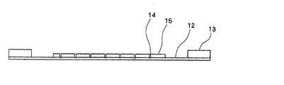
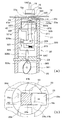
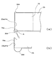
- an adhesive holding sheet 12 is attached to the back surface of the wafer 11, and the holding sheet 12 is attached to a metal ring 13.
- the wafer 11 is handled in such a state that it is attached to the metal ring 13 via the holding sheet 12 in this way.
- the wafer 11 is cut by a dicing saw or the like from the surface side into a semiconductor die 15 in the cutting process.
- a notch gap 14 formed during dicing is formed between the semiconductor dies 15. The depth of the cut gap 14 reaches from the semiconductor die 15 to a part of the holding sheet 12, but the holding sheet 12 is not cut and each semiconductor die 15 is held by the holding sheet 12.
- the wafer holder 10 includes an annular expand ring 16 having a flange portion and a ring presser 17 for fixing the ring 13 on the flange of the expand ring 16.
- the ring retainer 17 is driven in a direction to advance and retract toward the flange of the expand ring 16 by a ring retainer drive unit (not shown).
- the inner diameter of the expand ring 16 is larger than the diameter of the wafer on which the semiconductor die 15 is arranged, the expand ring 16 has a predetermined thickness, and the flange is outside the expand ring 16 and is separated from the holding sheet 12.
- the wafer holder 10 is configured to be movable in a direction along the surface of the holding sheet 12 by a wafer holder horizontal direction drive unit (not shown).
- the holding sheet 12 to which the semiconductor die 15 is attached is in a substantially planar state before being set on the expanding ring 16.
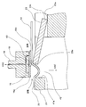
- FIG. 4 is a diagram showing a configuration of the semiconductor die pick-up apparatus 100, and FIG. 4 shows a state in which the semiconductor die 15 attached to the holding sheet 12 is set in the semiconductor die pick-up apparatus 100.
- the ring presser 17 is lowered on the ring 13, and the ring 13 is sandwiched between the flanges of the expand ring 16. Since there is a step between the upper surface where the holding sheet 12 of the expand ring 16 contacts and the flange surface, when the ring 13 is pressed against the flange surface, the holding sheet 12 is the same as the step between the upper surface of the expand ring 16 and the flange surface. It is stretched along the curved surface at the top of the expanding ring.
- the holding sheet 12 fixed on the expand ring 16 is subjected to a pulling force from the center of the holding sheet toward the periphery. Further, since the holding sheet 12 is extended by this tensile force, a gap between the semiconductor dies 15 attached on the holding sheet 12 is widened.
- the wafer holder 10 is attached with a wafer holder horizontal direction drive unit 72 that moves the wafer holder along a surface along the holding sheet 12.
- the wafer holder horizontal direction driving unit 72 may be, for example, a unit that drives the wafer holder 10 in the horizontal direction by a motor and a gear provided inside, or along a guide by a driving source such as a motor provided outside.
- the wafer holder 10 may be moved in the XY direction.
- a collet 18 for attracting and moving the semiconductor die 15 is provided on the wafer holder 10.
- the collet 18 includes suction holes 19 for sucking the semiconductor die 15 on the suction surface, and each suction hole 19 is connected to a vacuum device 71.
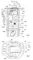
- a stage 20 is provided below the wafer holder 10, and the stage 20 is driven in a vertical direction that is a forward / backward direction with respect to the holding sheet 12 by a stage vertical direction driving mechanism 73.
- the stage vertical direction drive mechanism 73 may be, for example, a mechanism that drives the stage 20 in the vertical direction by a motor and a gear provided inside, or is vertically moved along a guide by a drive source such as a motor provided outside.
- the stage 20 may be moved in a driving direction.
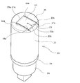
- the stage 20 has a cylindrical casing 21 having a close contact surface 22 in close contact with the holding sheet 12 on the upper surface thereof, and a base portion 24 provided on the opposite side of the close contact surface 22 of the casing 21. And a drive unit 25 that is attached to the base unit 24 and drives a slider drive mechanism 300 attached to the inside of the housing 21.
- the base portion 24 of the stage 20 is attached to a stage fixing portion (not shown).
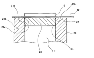
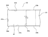
- the suction opening 41 is provided in the contact surface 22, is substantially the same width as the semiconductor die 15 to be picked up shown in FIG. 4, and is longer than the semiconductor die 15, from the inner peripheral side of the stage 20 toward the outer peripheral side. It extends in a straight line.
- a lid 23 that slides along the direction in which the suction opening 41 extends and opens and closes the suction opening 41 is attached to the suction opening 41.
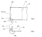
- the side of the lid 23 that closes the suction opening 41 along the sliding direction is the front end 23a, and the end on the side where the lid 23 opens is the rear end 23c.
- the side surface 23b of the lid 23 and the side surface 41b of the suction opening 41 constitute a slide surface. If the suction opening 41 has substantially the same width as the semiconductor die 15 to be picked up on the contact surface 22, a step is provided inside, and a slit communicating with the stage 20 is provided in the step portion. May be.
- the tip 23a of the lid 23 is a curved surface that is convex toward the side of closing the suction opening 41, and the end surface 41 a of the suction opening against which the tip 23 a of the lid 23 is pressed has a curved surface along the curved surface of the tip 23 a of the lid 23.
- the curved surface may be a cylindrical surface, a combination of cylindrical surfaces having a plurality of radii, or a curved surface having another shape.
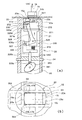
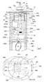
- a longitudinal groove 364 that extends in the direction and sucks the holding sheet 12 is provided.
- the vertical groove 364 is configured by a fan-shaped cylindrical surface of approximately 270 degrees connected to the suction opening 41, and the tangent line 500 that contacts the cylindrical surface of each vertical groove 364 at both corners of the suction opening 41 is the cylindrical surface of the end surface 41a. It protrudes from the end face 41a in the direction in which the lid 23 is closed to a position that becomes a tangent.
- a vertical groove 364 having a fan-shaped cylindrical surface of approximately 270 degrees communicates the contact surface 22 and the inside of the housing 21.
- 7B when the one end 15a of the semiconductor die 15 is aligned with the end face 41a of the suction opening 41 or the tip 23a of the lid 23, a part of the semiconductor die 15 is part of the tip of the lid 23.
- the fan-shaped hatched portion that protrudes from 23 a and is approximately 90 degrees is located above the vertical groove 364.
- the surface on the holding sheet 12 side becomes substantially flush with the contact surface 22.
- a chamfer 23 e is provided around the surface of the lid 23, and when the lid 23 closes the suction opening 41, a small V-shaped groove is formed between the contact surface 22 and the lid 23.
- the width of the suction opening 41, the width of the lid 23, and the width of the semiconductor die 15 are substantially the same, and the side surfaces 41b of the suction opening 41 and the side surfaces 23b of the lid 23 slide. Touching.
- the stage 20 is recessed from the contact surface 22 by the thickness of the lid 23, and is substantially the same width as the lid 23 from the end of the suction opening 41 on the side where the lid 23 opens to the outer peripheral side of the stage 20.
- a slide groove 22a is provided that slides while the rear end 23c of the lid 23 or the surface of the lid 23 opposite to the holding sheet is in contact with the surface.
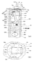
- a slider drive mechanism 300 for sliding a slider 332 to which a lid 23 is rotatably attached is provided inside the stage 20.
- the slider drive mechanism 300 is slidably attached to the first link 326 driven in the forward and backward direction with respect to the contact surface 22 by the drive unit 25 attached to the base portion 24 of the stage 20 and the housing 21 of the stage 20.
- a piston 370 that moves forward and backward with respect to the contact surface 22; a stopper 321a that is provided inside the housing 21 and that engages with a flange 371 of the piston 370 to limit the movement of the piston 370 in the forward / backward direction; A spring 373 that connects one link 326 and the piston 370 in a direction that advances and retreats with respect to the contact surface 22; a guide rail 331 that is attached to the piston 370 and extends substantially parallel to the contact surface 22 and extends in the direction of the suction opening 41; A slider 332 slidably attached to the guide rail 331 and a piston 370 can be freely rotated by a pin 328.
- a cylindrical pin 330 extending in the width direction of the suction opening 41 is attached to the slider 332, and an inverted U-shape provided on an arm 23 f that protrudes from the tip 23 a of the lid 23 toward the closing side of the suction opening 41.
- the mold notch is rotatably engaged.
- casing 21 is connected to the vacuum apparatus 71, and is comprised so that an inside can be made into a vacuum.
- the pin 327 provided at one end enters the engagement groove 326a of the first link 326, and the engagement groove 329a provided at the other end sandwiches the pin 330a of the slider 332, whereby the first link 326 and the first link 326 are engaged with the first link 326.
- a link 326 is connected.
- a motor 381 for operating the slider drive mechanism 300 is attached inside the drive unit 25, and a cam that contacts a roller 326 c provided at the tip of the shaft 326 b of the first link 326 on the rotating shaft of the motor 381. 383 is attached.
- the slider drive mechanism 300 changes the operation of the first link 326 that moves in the forward and backward direction toward the contact surface 22 to the operation in the direction in which the slider 332 is moved in parallel with the contact surface 22 by the L-shaped second link 329. Since it is converted, the structure can be made compact, and the mechanism can be stored inside the cylindrical casing 21.
- a semiconductor die pick-up device 100 includes a control unit 70 which is a computer including a CPU and the like, and includes a driving unit 25, a vacuum device 71, a collet 18, a wafer holder horizontal driving unit 72, a stage.
- the vertical drive mechanism 73 is connected to each other, and the drive unit 25, vacuum device 71, collet 18 and wafer holder horizontal drive unit 72, and stage vertical drive mechanism 73 are configured to be driven by commands output from the control unit 70.
- a one-dot chain line indicates a signal line that connects the control unit 70, the drive unit 25, the vacuum device 71, the collet 18, the wafer holder horizontal direction drive unit 72, and the stage vertical direction drive mechanism 73.
- FIGS. 1 to 8 The portions described with reference to FIGS. 1 to 8 are denoted by the same reference numerals, and description thereof is omitted.
- the control unit 70 starts the alignment process between the lid 23 and the semiconductor die 15 with the lid 23 closed. Since the lid 23 is in a position where the suction opening 41 is closed, the tip 23a of the lid 23 is in contact with the end surface 41a of the suction opening 41, and the lower surface of the rear end 23c of the lid 23 is the surface of the slide groove 22a. And is supported by the slide groove 22a. Further, the surface of the lid 23 and the contact surface 22 are substantially the same surface.
- the controller 70 moves the wafer holder 10 horizontally above the standby position of the stage 20 by the wafer holder horizontal direction driving unit 72 shown in FIG.
- the controller 70 once stops the horizontal movement of the wafer holder 10, and the stage 20 is driven by the stage vertical direction drive mechanism 73.
- the stage 20 is raised until the surface 22 and the surface of the lid 23 are in close contact with the lower surface of the holding sheet 12.
- the control unit 70 stops raising the stage 20.
- the control unit 70 again aligns the end 15a of the semiconductor die 15 to be picked up with the tip 23a of the lid 23 in the closed state by the wafer holder horizontal direction driving unit 72, and the position in the width direction of the lid 23 and the position of the semiconductor die 15
- the width direction position is adjusted and adjusted so that the side surface of the semiconductor die 15 matches the side surface 23 b of the lid 23. Since the width of the lid 23 is substantially the same as that of the semiconductor die 15 to be picked up, the position of each side surface of the semiconductor die 15 and each side surface 23b of the lid 23 when the one side surface 23b is aligned with the side surface of the semiconductor die 15. Can be combined.
- the holding sheet 12 receives a tensile force by the expanding ring 16 of the wafer holder 10.
- FIG. 9B is a plan view of the contact surface 22 of the stage 20 and the surface of the lid 23.
- the holding sheet 12 and the semiconductor die 15 placed thereon are indicated by a one-dot chain line so that the positional relationship can be understood.
- the lid 23 is shown slightly larger than the semiconductor die 15 in order to distinguish between the semiconductor die 15 and the lid 23 having substantially the same width.
- FIG. 10B, FIG. 12B, and FIG. 17B to FIG. 19B As shown in FIG. 9 (b), when the positions of the lid 23 and the semiconductor die 15 are aligned, the approximately 90-degree fan-shaped hatched portion of the semiconductor die 15 is located on the vertical groove 364.
- the control unit 70 ends the alignment process. Then, the control unit 70 moves to the position immediately above the semiconductor die 15 from which the collet 18 is to be picked up, and holds the collet 18 at a height with a slight gap. When the movement of the collet 18 is finished, the control unit 70 starts sucking air from the suction hole 19 by the vacuum device 71, and puts the collet 18 in a suction standby state of the semiconductor die 15.
- the control unit 70 starts the holding sheet peeling process.
- the control unit 70 evacuates the inside of the casing 21 of the stage 20 using the vacuum device 71.
- the vertical groove 364 communicating with the inside of the housing 21 shown in FIG. 10B is also evacuated, and the holding sheet 12 is attracted to the contact surface 22.
- the holding sheet 12 is pulled downward by the vacuum, but in this state, the holding sheet 12 is not yet peeled from the semiconductor die 15.
- the pressure in the V-shaped groove is lower than the atmospheric pressure, but the holding sheet 12 is not peeled off at this negative pressure.
- the cam 383 attached to the shaft of the motor 381 is rotated.
- the cam 383 has an elliptical shape, and the cam surface is in contact with the roller 326c attached to the tip of the shaft 326b of the first link 326.
- the cam 383 rotates in the direction of the arrow in FIG. Push up in the direction of 22.
- the shaft 326 b rises and the entire first link 326 rises toward the contact surface 22.
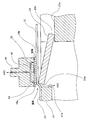
- the tip 23 a of the lid 23 advances upward from the contact surface 22, the tip 23 a of the lid 23 pushes up the holding sheet 12 and one end 15 a of the semiconductor die 15. Then, since the tip 23 a receives a downward force from the holding sheet 12, the lid 23 rotates clockwise about the pin 330.
- the rear end 23c of the lid 23 is supported by the surface of the slide groove 22a, and the surface of the rear end 23c on the holding sheet 12 side is substantially flush with the contact surface 22, so that the holding sheet 12 of the lid 23 is pushed up.
- the surface of the lid 23 is inclined downward from the front end 23a side to the rear end 23c side.
- the lid 23 pushes up the semiconductor die 15 and the holding sheet 12 to be picked up.
- the holding sheets 12 at both corners of the semiconductor die 15 located on the vertical grooves 364 that have become vacuum are sucked and fixed to the contact surface 22.
- the holding sheet 12 attached to the semiconductor die 15 to be picked up is pulled obliquely downward toward the contact surface 22, and the diagonal downward pulling force causes the holding sheet 12 to be placed on the vertical groove 364.
- the holding sheet 12 begins to peel from both corners of the semiconductor die 15 positioned, and the approximately 90-degree fan-shaped holding sheet 12 positioned on the longitudinal groove 364 is peeled off.
- the holding sheet 12 of the substantially triangular portion of the semiconductor die 15 that protrudes from the tip 23 a of the lid 23 to the contact surface 22 is pulled obliquely downward toward the contact surface 22.
- the semiconductor die 15 is peeled from both sides in the width direction toward the center in the width direction.
- the peeling line 53 is formed at a position slightly closer to the sliding direction of the lid 23 than the one end 15 a of the semiconductor die 15.
- the portion of the semiconductor die 15 from which the holding sheet 12 is peeled loses the force drawn toward the contact surface 22 by the holding sheet 12.
- the pressure on the collet 18 side surface of the semiconductor die is reduced by approaching the adsorption surface of the collet 18 by the upward movement of the tip 23a of the lid 23.
- the pressure of the surface of the semiconductor die 15 on the holding sheet 12 side becomes higher than the pressure on the collet 18 side, and the portion of the semiconductor die 15 peeled off from the holding sheet 12 is adsorbed by the collet 18.
- a portion of the semiconductor die 15 on the rear end 23c side of the lid 23 from the peeling line 53 where the holding sheet 12 has not yet been peeled is left with a slight gap between the semiconductor die 15 and the collet 18. Since the pressure difference between the holding sheet 12 side and the collet 18 side is not so large and there is a pulling force by the holding sheet 12, it is not yet adsorbed by the collet 18. For this reason, the semiconductor die 15 undergoes minute bending deformation between a portion adsorbed by the collet 18 and a portion not adsorbed by the collet 18.
- the peeling line 53 is a line extending from the side surface in the width direction of the semiconductor die 15 to the side surface along the tip 23 a of the lid 23, and in the portion along the side surface 23 b of the lid 23.
- the peeling line 53 does not extend.
- each side surface 23b of the lid 23 is in contact with each side surface 41b of the suction opening 41.
- the lower surface of the rear end 23c of the lid 23 is in contact with the surface of the slide groove 22a.
- the holding sheet 12 peeled off from the semiconductor die 15 is covered on the vertical groove 364. For this reason, since almost no air flows from the outside of the housing 21 toward the inside of the housing 21, the inside of the housing 21 is kept in a vacuum.
- the spring 373 of the slider drive mechanism 300 has such a stiffness that it hardly bends when the tip 23 a of the lid 23 is pushed up from the contact surface 22, the tip 23 a of the lid 23 has a predetermined advance height from the contact surface 22. Even if pushed up, the distance between the piston 370 and the first link 326 hardly changes. For this reason, the lid 23 only protrudes from the contact surface 22 by the rising of the first link 326 and does not slide.
- the pin 328 of the piston 370 does not rise with respect to the contact surface 22, and only the pin 327 of the second link 329 entering the engagement groove 326 a of the first link 326 rises in the direction of the contact surface 22. Then, the second link 329 starts to rotate around the pin 328. By this rotation operation, the engaging groove 329a at the other end of the second link 329 moves toward the outer periphery of the stage 20, and the slider 332 and the pin of the slider 332 to which the pin 330a in the engaging groove 329a is fixed.
- the lid 23 that is rotatably engaged with the 330 via the arm 23 f starts to slide toward the outer peripheral side of the stage 20.
- the tip 23a of the lid 23 is separated from the end face 41a of the suction opening 41, and the suction opening 41 is opened to have an opening having substantially the same width as the semiconductor die 15 to be picked up.
- An opening 42 is formed. Since the inside of the housing 21 of the stage 20 is in a vacuum state by the vacuum device 71, the opening opening 42 sucks the holding sheet 12 therein. Then, the holding sheet 12 is drawn into the opening portion 42 as the lid 23 slides, and is peeled off from the semiconductor die 15.
- the center in the width direction of the lid 23 from the adhesion surface 22 is a ridge line that rises in a mountain shape.
- each side surface 23 b side of the lid 23 is a line inclined toward the sliding direction from the center portion. For this reason, the holding sheet 12 on each side of the semiconductor die 15 is peeled off before the holding sheet 12 at the center portion in the width direction of the semiconductor die 15.
- the peeling line 53 is inclined with respect to the ends 15a and 15b of the semiconductor die 15 or with respect to the sliding direction in the plane along the contact surface 22, the portion adsorbed by the collet 18 and the collet The stress generated by a minute bending deformation between the portion not adsorbed by 18 is relieved, and damage to the semiconductor die 15 can be effectively suppressed.
- the opening portion 42 increases toward the outer peripheral side of the stage 20, and the peeling line 53 sequentially moves in parallel to the outer peripheral side of the stage 20.
- the holding sheet 12 is sequentially peeled from the one end 15 a to the other end 15 b of the semiconductor die 15 along the peeling line 53, and is sequentially sucked into the opening opening 42.
- the rear end 23c of the lid 23 moves downward from the contact surface 22, so that the rear end 23c of the lid 23 may hit the adjacent semiconductor die 15 when the lid 23 is slid.
- the adjacent semiconductor die 15 is not damaged by the slide of the lid 23, the semiconductor die 15 can be easily picked up even when there are adjacent semiconductor dies 15.
- the opening portion 42 is covered by the peeled holding sheet 12, but the holding sheet 12 is sucked into the opening portion 42, and the tip 23 a of the lid 23 faces the portion where the holding sheet 12 is not peeled off. Therefore, the suction of the holding sheet 12 by the opening 42 is not stopped, and the entire holding sheet 12 is sequentially sucked from the one end 15a of the semiconductor die 15 to the other end 15b by the opening 42. It can be peeled off and the remaining part of the peeling can be prevented.
- the semiconductor die 15 is entirely adsorbed by the collet 18 and picked up by the collet 18.
- the cam 383 of the slider drive mechanism 300 After the semiconductor die 15 is picked up, when the cam 383 of the slider drive mechanism 300 further rotates according to a command from the control unit 70, the shaft 326b of the first link 326 is lowered due to the rotation of the cam 383.
- the lid 23 closes the suction opening 41 when the tip 23a is in contact with the end face 41a, sliding in the direction toward the end face 41a of the suction opening 41. Then, the compression force of the spring 373 is released.
- the cam 383 further rotates and the shaft 326b is lowered, the piston 370, the first link 326, and the second link 329 are both lowered, and the tip 23a of the lid 23 is lowered to substantially the same position as the surface of the contact surface 22. To return to the initial position.
- the lid 23 is slid in a state where the lid 23 is advanced upward from the contact surface 22 of the tip 23a, and the width of the semiconductor die 15 appears almost directly below the semiconductor die 15.
- the holding sheet 12 is sequentially peeled off, and the semiconductor dies 15 are sequentially attracted to the collet 18 waiting immediately above the semiconductor die 15. Therefore, the semiconductor die 15 can be easily picked up while suppressing the force applied to the semiconductor die 15 when the holding sheet 12 is peeled off.
- the tip 23a of the lid 23 is advanced upward from the contact surface 22 in a state where the vertical groove 364 is evacuated, and the semiconductor die 15 is pushed up and picked up by the downward pulling force generated in the holding sheet 12. Since a trigger for peeling is created by peeling off the holding sheets 12 at both corners of the one end 15a of the semiconductor die 15, and then the lid 23 is slid to suck the holding sheet 12 into the opening 42, There is an effect that the holding sheet 12 can be peeled off more easily.
- the lid 23 is slid from the one end 15a side to the other end 15b side of the semiconductor die 15, and the holding sheet 12 is sequentially sucked into the opening opening 42 to peel off the holding sheet 12. Even if the opening portion 42 is covered by the holding sheet 12 sucked into the opening portion 42, the lid 23 slides toward the portion where the holding sheet 12 is not peeled, so that the entire holding sheet 12 is sequentially opened. The opening 42 can be sucked and peeled off, and the entire holding sheet 12 can be easily peeled off.
- the tip 23 a of the lid 23 is a curved surface
- the peeling line 53 is inclined with respect to the ends 15 a and 15 b of the semiconductor die 15 or with respect to the sliding direction within the plane along the contact surface 22.
- the part that advances upward from the contact surface 22 is a part of the vicinity of the tip 23a of the lid 23, and the rear end 23c of the lid 23 does not advance upward from the contact surface 22, so that the lid 23 is slid.
- the rear end 23c of the lid 23 does not collide with the adjacent semiconductor die 15, and the adjacent semiconductor die 15 is not damaged by the sliding of the lid 23. Therefore, even when there are adjacent semiconductor dies 15 around The semiconductor die 15 can be picked up.
- the stage 20 includes only a vertical movement in the advancing and retreating direction with respect to the holding sheet 12 by the stage vertical driving mechanism 73, and a moving mechanism with respect to the horizontal direction that is along the holding sheet 12. Therefore, there is no backlash of the mechanism in the horizontal direction, and the position stability in the direction along the holding sheet 12 is good. Further, since the alignment of the semiconductor die 15 to be picked up and the lid 23 in the direction along the surface of the holding sheet 12 is performed by the wafer holder horizontal direction driving unit 72, the horizontal position of the stage 20 is adjusted during the horizontal alignment. Is stable, and it is possible to reduce the occurrence of misalignment during alignment between the lid 23 of the stage 20 and the semiconductor die 15 attached to the holding sheet 12.
- FIGS. 1 to 13 Parts similar to those of the embodiment described with reference to FIGS. 1 to 13 are denoted by the same reference numerals and description thereof is omitted.
- the stage 20 of the semiconductor die pickup apparatus 100 of the present embodiment is provided on the contact surface 22 as in the embodiment described above with reference to FIG. 5, and the pickup shown in FIG.
- a suction opening 41 that is substantially the same width as the semiconductor die 15 and longer than the semiconductor die 15 and extends linearly from the inner peripheral side of the stage 20 toward the outer peripheral side, and the width of the suction opening 41 is substantially the same.
- the lid 23 has the same width and slides along the extending direction of the suction opening 41 to open and close the suction opening 41.
- the side of the lid 23 that closes the suction opening 41 along the sliding direction is the front end 23a, and the end on the side where the lid 23 opens is the rear end 23c.
- the side surface 23b of the lid 23 and the side surface 41b of the suction opening 41 constitute a slide surface.
- the lid 23 is rectangular, the tip 23a of the lid 23 is flat, and the end surface 41a of the suction opening 41 that the tip 23a contacts when the lid 23 is closed is also flat.
- a longitudinal groove 364 that extends in the direction and sucks the holding sheet 12 is provided.
- the longitudinal groove 364 is configured by a fan-shaped cylindrical surface of approximately 180 degrees connected to the suction opening 41.
- a vertical groove 364 having a fan-shaped cylindrical surface of approximately 180 degrees communicates the contact surface 22 and the inside of the housing 21. 7B, when the one end 15a of the semiconductor die 15 is aligned with the end face 41a of the suction opening 41 or the tip 23a of the lid 23, the semiconductor die 15 is placed on the tip 23a of the lid 23. To position.
- the control unit 70 starts the alignment process between the lid 23 and the semiconductor die 15 with the lid 23 closed.
- the control unit 70 aligns one end 15a of the semiconductor die 15 to be picked up with the tip 23a of the lid 23 in the closed state by the wafer holder horizontal direction driving unit 72 shown in FIG. 15 is adjusted so that the side surface of the semiconductor die 15 matches the side surface 23 b of the lid 23. Since the width of the lid 23 is substantially the same as that of the semiconductor die 15 to be picked up, the position of each side surface of the semiconductor die 15 and each side surface 23b of the lid 23 when the one side surface 23b is aligned with the side surface of the semiconductor die 15. Can be combined. As shown in FIG. 17B, when the positions of the lid 23 and the semiconductor die 15 are aligned, the semiconductor die 15 is positioned on the lid 23.
- the control unit 70 ends the alignment process. Then, the control unit 70 moves to the position immediately above the semiconductor die 15 from which the collet 18 is to be picked up, and holds the collet 18 at a height with a slight gap. When the movement of the collet 18 is finished, the control unit 70 starts sucking air from the suction hole 19 by the vacuum device 71, and puts the collet 18 in a suction standby state of the semiconductor die 15.
- control unit 70 starts the holding sheet peeling process.
- the control unit 70 evacuates the inside of the casing 21 of the stage 20 using the vacuum device 71.
- the vertical groove 364 communicating with the inside of the housing 21 shown in FIG. 17B is also evacuated, and the holding sheet 12 adjacent to the semiconductor die 15 is brought into close contact with the surface. Adsorb to 22.
- the lid 23 pushes up the semiconductor die 15 and the holding sheet 12 to be picked up.
- the holding sheet 12 positioned on the vertical groove 364 that has been evacuated is sucked and fixed to the contact surface 22.
- the holding sheet 12 attached to the semiconductor die 15 to be picked up is pulled obliquely downward toward the contact surface 22, and in the vicinity of the vertical groove 364 by this oblique downward pulling force.
- the holding sheets 12 at both corners of the semiconductor die 15 are peeled off slightly. As shown in FIG.
- the lid 23 rotates as the tip 23 a of the lid 23 rises, so that the tip 23 a of the lid 23 is slightly closer to the sliding direction of the lid 23 than the one end 15 a of the semiconductor die 15.
- the holding sheet 12 in this portion is peeled off from the semiconductor die 15, and a peeling line 53 is formed at a position slightly closer to the sliding direction of the lid 23 than the one end 15 a of the semiconductor die 15. Then, the semiconductor die 15 in the portion up to the one end 15 a of the semiconductor die 15 and the separation line 53 is adsorbed by the collet 18.
- the tip 23a of the lid 23 is separated from the end surface 41a of the suction opening 41, and the suction opening 41 is opened to have an opening having substantially the same width as the semiconductor die 15 to be picked up.
- An opening 42 is formed, and the opening opening 42 sucks the holding sheet 12 therein.
- the holding sheet 12 is drawn into the opening portion 42 as the lid 23 slides, and is peeled off from the semiconductor die 15.
- the opening portion 42 becomes larger toward the outer peripheral side of the stage 20, and the peeling line 53 sequentially moves in parallel to the outer peripheral side of the stage 20.
- the holding sheet 12 is sequentially peeled from the one end 15 a to the other end 15 b of the semiconductor die 15 along the peeling line 53, and is sequentially sucked into the opening opening 42.
- the semiconductor die 15 is entirely adsorbed by the collet 18 and picked up by the collet 18.
- the semiconductor die 15 is peeled off when the holding sheet 12 is peeled off by a simpler configuration in which the tip 23a of the lid 23 and the end surface 41a of the suction opening 41 are configured as flat surfaces, as in the embodiment described above.
- the semiconductor die 15 can be easily picked up while suppressing the force applied to.
- the holding sheet 12 at both corners of the one end 15a of the semiconductor die 15 to be picked up is peeled off to create a trigger for peeling, and then the lid 23 is slid to suck the holding sheet 12 into the opening 42. Therefore, there is an effect that the holding sheet 12 can be peeled off more easily.
- the entire holding sheet 12 is sequentially sucked and peeled off by the opening portion 42, the entire holding sheet 12 can be easily peeled off. Further, the vacuum inside the casing 21 can be maintained well, and the holding sheet 12 can be effectively sucked into the opening portion 42 and peeled off.
Landscapes
- Container, Conveyance, Adherence, Positioning, Of Wafer (AREA)
- Die Bonding (AREA)
Applications Claiming Priority (2)
| Application Number | Priority Date | Filing Date | Title |
|---|---|---|---|
| JP2008-121460 | 2008-05-07 | ||
| JP2008121460A JP4198745B1 (ja) | 2008-05-07 | 2008-05-07 | 半導体ダイのピックアップ装置及びピックアップ方法 |
Publications (1)
| Publication Number | Publication Date |
|---|---|
| WO2009136450A1 true WO2009136450A1 (ja) | 2009-11-12 |
Family
ID=40239520
Family Applications (1)
| Application Number | Title | Priority Date | Filing Date |
|---|---|---|---|
| PCT/JP2008/061610 Ceased WO2009136450A1 (ja) | 2008-05-07 | 2008-06-26 | 半導体ダイのピックアップ装置及びピックアップ方法 |
Country Status (4)
| Country | Link |
|---|---|
| JP (1) | JP4198745B1 (enExample) |
| KR (1) | KR20110014569A (enExample) |
| TW (1) | TW200946427A (enExample) |
| WO (1) | WO2009136450A1 (enExample) |
Cited By (1)
| Publication number | Priority date | Publication date | Assignee | Title |
|---|---|---|---|---|
| US7820006B2 (en) | 2009-03-05 | 2010-10-26 | Shinkkawa Ltd. | Die pickup apparatus for picking up semiconductor dies and methods for picking up semiconductor dies |
Families Citing this family (5)
| Publication number | Priority date | Publication date | Assignee | Title |
|---|---|---|---|---|
| SG163493A1 (en) | 2009-01-22 | 2010-08-30 | Esec Ag | Die ejector |
| US9038264B2 (en) * | 2011-02-28 | 2015-05-26 | Sandisk Semiconductor (Shanghai) Co., Ltd. | Non-uniform vacuum profile die attach tip |
| TWI485786B (zh) * | 2012-04-16 | 2015-05-21 | Gallant Micro Machining Co Ltd | Grain Stripping Method and Device |
| CN108962807B (zh) * | 2018-09-07 | 2024-08-30 | 先进光电器材(深圳)有限公司 | 自动抓取机构 |
| CN113109357B (zh) * | 2021-04-09 | 2021-11-23 | 徐州盛科半导体科技有限公司 | 一种可拆卸的半导体分析装置 |
Citations (3)
| Publication number | Priority date | Publication date | Assignee | Title |
|---|---|---|---|---|
| JP2003264203A (ja) * | 2002-03-11 | 2003-09-19 | Hitachi Ltd | 半導体装置の製造方法 |
| JP2004327965A (ja) * | 2003-04-10 | 2004-11-18 | Matsushita Electric Ind Co Ltd | チップのピックアップ装置およびピックアップ方法 |
| JP2005197368A (ja) * | 2004-01-05 | 2005-07-21 | Shibaura Mechatronics Corp | 半導体チップのピックアップ装置及びピックアップ方法 |
-
2008
- 2008-05-07 JP JP2008121460A patent/JP4198745B1/ja not_active Expired - Fee Related
- 2008-06-26 KR KR1020107023438A patent/KR20110014569A/ko not_active Withdrawn
- 2008-06-26 WO PCT/JP2008/061610 patent/WO2009136450A1/ja not_active Ceased
- 2008-09-22 TW TW097136280A patent/TW200946427A/zh not_active IP Right Cessation
Patent Citations (3)
| Publication number | Priority date | Publication date | Assignee | Title |
|---|---|---|---|---|
| JP2003264203A (ja) * | 2002-03-11 | 2003-09-19 | Hitachi Ltd | 半導体装置の製造方法 |
| JP2004327965A (ja) * | 2003-04-10 | 2004-11-18 | Matsushita Electric Ind Co Ltd | チップのピックアップ装置およびピックアップ方法 |
| JP2005197368A (ja) * | 2004-01-05 | 2005-07-21 | Shibaura Mechatronics Corp | 半導体チップのピックアップ装置及びピックアップ方法 |
Cited By (1)
| Publication number | Priority date | Publication date | Assignee | Title |
|---|---|---|---|---|
| US7820006B2 (en) | 2009-03-05 | 2010-10-26 | Shinkkawa Ltd. | Die pickup apparatus for picking up semiconductor dies and methods for picking up semiconductor dies |
Also Published As
| Publication number | Publication date |
|---|---|
| KR20110014569A (ko) | 2011-02-11 |
| TW200946427A (en) | 2009-11-16 |
| JP4198745B1 (ja) | 2008-12-17 |
| JP2009272430A (ja) | 2009-11-19 |
| TWI353957B (enExample) | 2011-12-11 |
Similar Documents
| Publication | Publication Date | Title |
|---|---|---|
| JP4397429B1 (ja) | 半導体ダイのピックアップ装置及びピックアップ方法 | |
| JP4215818B1 (ja) | 半導体ダイのピックアップ装置及びピックアップ方法 | |
| JP4927979B2 (ja) | 半導体ダイのピックアップ装置及びその装置を用いた半導体ダイのピックアップ方法 | |
| JP2009064937A (ja) | 半導体ダイのピックアップ装置及びピックアップ方法 | |
| JP2009064938A (ja) | 半導体ダイのピックアップ装置及びピックアップ方法 | |
| JP6349496B2 (ja) | 半導体ダイのピックアップ装置及びピックアップ方法 | |
| JP4198745B1 (ja) | 半導体ダイのピックアップ装置及びピックアップ方法 | |
| KR100874367B1 (ko) | 다이 본더와 다이 본더의 열압착 테이프편 절취 및 첩부방법 및 프로그램을 기록한 컴퓨터 판독가능한 기록매체 |
Legal Events
| Date | Code | Title | Description |
|---|---|---|---|
| 121 | Ep: the epo has been informed by wipo that ep was designated in this application |
Ref document number: 08790625 Country of ref document: EP Kind code of ref document: A1 |
|
| ENP | Entry into the national phase |
Ref document number: 20107023438 Country of ref document: KR Kind code of ref document: A |
|
| NENP | Non-entry into the national phase |
Ref country code: DE |
|
| 122 | Ep: pct application non-entry in european phase |
Ref document number: 08790625 Country of ref document: EP Kind code of ref document: A1 |