WO2009099056A1 - 包絡線追跡電源回路及びそれを含む高周波増幅器 - Google Patents
包絡線追跡電源回路及びそれを含む高周波増幅器 Download PDFInfo
- Publication number
- WO2009099056A1 WO2009099056A1 PCT/JP2009/051771 JP2009051771W WO2009099056A1 WO 2009099056 A1 WO2009099056 A1 WO 2009099056A1 JP 2009051771 W JP2009051771 W JP 2009051771W WO 2009099056 A1 WO2009099056 A1 WO 2009099056A1
- Authority
- WO
- WIPO (PCT)
- Prior art keywords
- envelope
- power supply
- output
- supply circuit
- voltage
- Prior art date
- Legal status (The legal status is an assumption and is not a legal conclusion. Google has not performed a legal analysis and makes no representation as to the accuracy of the status listed.)
- Ceased
Links
Images


Classifications
-
- H—ELECTRICITY
- H03—ELECTRONIC CIRCUITRY
- H03F—AMPLIFIERS
- H03F1/00—Details of amplifiers with only discharge tubes, only semiconductor devices or only unspecified devices as amplifying elements
- H03F1/02—Modifications of amplifiers to raise the efficiency, e.g. gliding Class A stages, use of an auxiliary oscillation
- H03F1/0205—Modifications of amplifiers to raise the efficiency, e.g. gliding Class A stages, use of an auxiliary oscillation in transistor amplifiers
- H03F1/0211—Modifications of amplifiers to raise the efficiency, e.g. gliding Class A stages, use of an auxiliary oscillation in transistor amplifiers with control of the supply voltage or current
- H03F1/0216—Continuous control
- H03F1/0222—Continuous control by using a signal derived from the input signal
- H03F1/0227—Continuous control by using a signal derived from the input signal using supply converters
-
- H—ELECTRICITY
- H03—ELECTRONIC CIRCUITRY
- H03F—AMPLIFIERS
- H03F1/00—Details of amplifiers with only discharge tubes, only semiconductor devices or only unspecified devices as amplifying elements
- H03F1/02—Modifications of amplifiers to raise the efficiency, e.g. gliding Class A stages, use of an auxiliary oscillation
- H03F1/04—Modifications of amplifiers to raise the efficiency, e.g. gliding Class A stages, use of an auxiliary oscillation in discharge-tube amplifiers
- H03F1/06—Modifications of amplifiers to raise the efficiency, e.g. gliding Class A stages, use of an auxiliary oscillation in discharge-tube amplifiers to raise the efficiency of amplifying modulated radio frequency waves; to raise the efficiency of amplifiers acting also as modulators
-
- H—ELECTRICITY
- H02—GENERATION; CONVERSION OR DISTRIBUTION OF ELECTRIC POWER
- H02M—APPARATUS FOR CONVERSION BETWEEN AC AND AC, BETWEEN AC AND DC, OR BETWEEN DC AND DC, AND FOR USE WITH MAINS OR SIMILAR POWER SUPPLY SYSTEMS; CONVERSION OF DC OR AC INPUT POWER INTO SURGE OUTPUT POWER; CONTROL OR REGULATION THEREOF
- H02M3/00—Conversion of DC power input into DC power output
- H02M3/02—Conversion of DC power input into DC power output without intermediate conversion into AC
- H02M3/04—Conversion of DC power input into DC power output without intermediate conversion into AC by static converters
- H02M3/10—Conversion of DC power input into DC power output without intermediate conversion into AC by static converters using discharge tubes with control electrode or semiconductor devices with control electrode
- H02M3/145—Conversion of DC power input into DC power output without intermediate conversion into AC by static converters using discharge tubes with control electrode or semiconductor devices with control electrode using devices of a triode or transistor type requiring continuous application of a control signal
- H02M3/155—Conversion of DC power input into DC power output without intermediate conversion into AC by static converters using discharge tubes with control electrode or semiconductor devices with control electrode using devices of a triode or transistor type requiring continuous application of a control signal using semiconductor devices only
-
- H—ELECTRICITY
- H03—ELECTRONIC CIRCUITRY
- H03F—AMPLIFIERS
- H03F1/00—Details of amplifiers with only discharge tubes, only semiconductor devices or only unspecified devices as amplifying elements
- H03F1/02—Modifications of amplifiers to raise the efficiency, e.g. gliding Class A stages, use of an auxiliary oscillation
-
- H—ELECTRICITY
- H03—ELECTRONIC CIRCUITRY
- H03F—AMPLIFIERS
- H03F3/00—Amplifiers with only discharge tubes or only semiconductor devices as amplifying elements
- H03F3/189—High-frequency amplifiers, e.g. radio frequency amplifiers
-
- H—ELECTRICITY
- H03—ELECTRONIC CIRCUITRY
- H03F—AMPLIFIERS
- H03F3/00—Amplifiers with only discharge tubes or only semiconductor devices as amplifying elements
- H03F3/20—Power amplifiers, e.g. Class B amplifiers, Class C amplifiers
- H03F3/24—Power amplifiers, e.g. Class B amplifiers, Class C amplifiers of transmitter output stages
- H03F3/245—Power amplifiers, e.g. Class B amplifiers, Class C amplifiers of transmitter output stages with semiconductor devices only
-
- H—ELECTRICITY
- H02—GENERATION; CONVERSION OR DISTRIBUTION OF ELECTRIC POWER
- H02M—APPARATUS FOR CONVERSION BETWEEN AC AND AC, BETWEEN AC AND DC, OR BETWEEN DC AND DC, AND FOR USE WITH MAINS OR SIMILAR POWER SUPPLY SYSTEMS; CONVERSION OF DC OR AC INPUT POWER INTO SURGE OUTPUT POWER; CONTROL OR REGULATION THEREOF
- H02M1/00—Details of apparatus for conversion
- H02M1/0045—Converters combining the concepts of switch-mode regulation and linear regulation, e.g. linear pre-regulator to switching converter, linear and switching converter in parallel, same converter or same transistor operating either in linear or switching mode
-
- H—ELECTRICITY
- H03—ELECTRONIC CIRCUITRY
- H03F—AMPLIFIERS
- H03F2200/00—Indexing scheme relating to amplifiers
- H03F2200/102—A non-specified detector of a signal envelope being used in an amplifying circuit
-
- H—ELECTRICITY
- H03—ELECTRONIC CIRCUITRY
- H03F—AMPLIFIERS
- H03F2200/00—Indexing scheme relating to amplifiers
- H03F2200/195—A hybrid coupler being used as power measuring circuit at the input of an amplifier circuit
-
- H—ELECTRICITY
- H03—ELECTRONIC CIRCUITRY
- H03F—AMPLIFIERS
- H03F2200/00—Indexing scheme relating to amplifiers
- H03F2200/451—Indexing scheme relating to amplifiers the amplifier being a radio frequency amplifier
-
- Y—GENERAL TAGGING OF NEW TECHNOLOGICAL DEVELOPMENTS; GENERAL TAGGING OF CROSS-SECTIONAL TECHNOLOGIES SPANNING OVER SEVERAL SECTIONS OF THE IPC; TECHNICAL SUBJECTS COVERED BY FORMER USPC CROSS-REFERENCE ART COLLECTIONS [XRACs] AND DIGESTS
- Y02—TECHNOLOGIES OR APPLICATIONS FOR MITIGATION OR ADAPTATION AGAINST CLIMATE CHANGE
- Y02B—CLIMATE CHANGE MITIGATION TECHNOLOGIES RELATED TO BUILDINGS, e.g. HOUSING, HOUSE APPLIANCES OR RELATED END-USER APPLICATIONS
- Y02B70/00—Technologies for an efficient end-user side electric power management and consumption
- Y02B70/10—Technologies improving the efficiency by using switched-mode power supplies [SMPS], i.e. efficient power electronics conversion e.g. power factor correction or reduction of losses in power supplies or efficient standby modes
Definitions
- the present invention relates to an envelope tracking power supply circuit and a high-frequency amplifier including the same.
- a power supply circuit for improving the efficiency of a high-frequency power amplifier is an envelope tracking power supply circuit that changes the power supply voltage applied to the high-frequency amplifier following the envelope of a radio signal input to the high-frequency amplifier.
- the envelope tracking power supply circuit receives a signal corresponding to the envelope of the input signal of the power amplifier, and includes a portion including an operational amplifier that is a wide-band power supply and a narrow-band but high-efficiency power supply compared to the operational amplifier. And a portion including a switching converter.
- Such an envelope tracking power supply circuit amplifies a signal whose peak power is higher than the average power when used for a communication method such as WCDMA (Wideband Code Division Multiple Access) or OFDM (Orthogonal Frequency Division Multiplexing). This is effective when used as a power amplifier for a radio base station.
- WCDMA Wideband Code Division Multiple Access
- OFDM Orthogonal Frequency Division Multiplexing
- the slew rate of the input envelope signal is widely distributed, and the conventional envelope tracking power supply circuit described above is designed to be optimized for the average value of the slew rate.
- Efficiency drops in many time zones that deviate from the average slew rate. That is, when the slew rate of the envelope signal exceeds the slew rate that can be handled by the switching converter, the efficiency decreases because all the alternating current is covered by the operational amplifier.
- the slew rate of the envelope signal is lower than the slew rate that can be handled by the switching converter, the efficiency is reduced by the amount that the switching converter is designed for the average slew rate. Even if it is small, it is kept constant with its low efficiency.
- the present invention has been made in view of such problems, and provides an envelope tracking power supply circuit and a high frequency amplifier that can maintain high efficiency even for a high frequency signal having a broadband envelope. For the purpose.
- an envelope tracking power supply circuit is an envelope tracking power supply circuit that generates an output voltage corresponding to an envelope of a high-frequency signal, and an envelope signal corresponding to the envelope is input.
- a voltage follower circuit section that outputs a voltage according to the envelope signal, first and second parallel resistors connected in parallel between the output of the voltage follower circuit and the output terminal of the output voltage, The first and second hysteresis comparator units that detect the respective voltage drops in the first and second parallel resistors and generate a voltage corresponding to the voltage drop, and the first and second hysteresis comparator units, respectively, And first and second switching converter units that switch in accordance with the output voltage and output the voltage to the output terminal.
- the current output from the voltage follower circuit unit via the first parallel resistor and the first switching that is performed according to the detection of the current by the first hysteresis comparator unit.
- a second switching converter that switches according to a current output from the switching converter unit, a current output from the voltage follower circuit unit via the second parallel resistor, and detection of the current by the second hysteresis comparator unit The current output from the unit is combined and output to the output terminal.
- an output corresponding to the level of the envelope signal is obtained at the output terminal, a circuit unit including the first hysteresis comparator unit and the first switching converter unit, a second hysteresis comparator unit, and a second hysteresis comparator unit.
- the envelope tracking power supply circuit of the present invention high efficiency can be maintained even for a high-frequency signal having a broadband envelope.
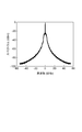
- FIG. 1 is a circuit diagram showing a schematic configuration of a high-frequency amplifier according to a preferred embodiment of the present invention. It is a graph which shows the time change of the voltage of the output RF signal of the power amplifier of FIG. 1, and the output voltage of an envelope tracking power supply circuit. It is a basic circuit diagram for demonstrating the principle of an envelope tracking system. It is a graph which shows the spectrum distribution of the envelope signal in the mobile communication system of WCDMA.
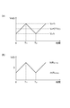
- (A) is a graph which shows the time change of the output voltage from the switching converter of FIG. 3
- (b) is a graph which shows the time change of the output current from the switching converter of FIG.
- It is a graph which shows the input-output waveform in the basic circuit of FIG.
- SYMBOLS 1 High frequency amplifier, 5 ... Envelope tracking power supply circuit, 7 ... Voltage follower circuit, 9a, 9b ... Hysteresis comparator, 11a, 11b ... Switching converter, 13a, 13b ... Semiconductor switch, 17a, 17b ... Inductor, 19a, 19b ... Power generation unit, R sense ... parallel resistance.
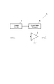
- FIG. 1 is a circuit diagram showing a schematic configuration of a high-frequency amplifier 1 according to a preferred embodiment of the present invention.
- a high-frequency amplifier 1 shown in FIG. 1 is for amplifying a radio signal in a radio base station for mobile communication, and includes an envelope detector 3, an envelope tracking power supply circuit 5, and a power amplifier 4. .
- the power amplifier 4 receives power supplied from the envelope tracking power supply circuit 5 and amplifies and outputs an input high-frequency radio signal (hereinafter referred to as an RF signal).
- the envelope detector 3 detects an envelope by detection or the like, and inputs an envelope signal to the envelope tracking power supply circuit 5.
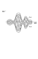
- FIG. 2 shows an example of temporal changes in the voltage S out0 of the output RF signal of the power amplifier 4 and the output voltage S out1 of the envelope tracking power supply circuit 5.
- the envelope tracking power supply circuit 5 generates an output voltage corresponding to the time variation of the envelope of the RF signal.
- FIG. 3 is a basic circuit diagram for explaining the principle of the envelope tracking method.
- An envelope tracking basic circuit 905 includes a voltage follower circuit 907 composed of an operational amplifier to which an envelope signal S E is input, and a resistance element R sense connected between the voltage follower circuit 907 and the output of the basic circuit 905.
- a hysteresis comparator 909 that detects a voltage drop in the resistance element R sense and compares the potentials at both ends thereof, and a switching converter 911 that receives and switches the output of the hysteresis comparator 909.
- the switching converter 911 has a semiconductor switch 913 such as a power MOSFET in which a bias voltage V dd is applied to the drain terminal and an output of the hysteresis comparator 909 is connected to the gate terminal, an anode terminal is grounded, and a cathode terminal is the semiconductor switch 913.
- the diode 915 is connected to the source terminal, and the inductor 917 is connected between the source terminal of the semiconductor switch 913 and the output of the basic circuit 905.
- the power amplifier 4 is equivalently replaced with a load resistance R load .
- the semiconductor switch 913 when the output voltage of the hysteresis comparator 909 is high and the semiconductor switch 913 is in the on state, the current from the switching converter 911 increases and accordingly flows from the voltage follower circuit 907 to the load resistance R load . The current decreases. As a result, the voltage drop of the resistance element R sense is reduced and the output of the hysteresis comparator 909 becomes low, so that the semiconductor switch 913 is turned off. When the semiconductor switch 913 is in the OFF state, the current from the switching converter 911 decreases, and accordingly, the current flowing from the voltage follower circuit 907 to the load resistor R load increases. As a result, the voltage drop of the resistance element R sense increases and the output voltage of the hysteresis comparator 909 becomes high, so that the semiconductor switch 913 is turned on.
- the high frequency component (ripple) of the output voltage in the switching converter 911 is complemented (cancelled) by the output voltage of the voltage follower circuit 907, and the output voltage corresponding to the envelope signal S E is loaded. Resistor R load is generated.
- the voltage follower circuit 907 composed of an operational amplifier is a power supply having a wide band but a low efficiency, while the switching converter 911 is a power supply having a narrow band but a high efficiency.
- the spectrum distribution of the envelope signal in the WCDMA mobile communication system is concentrated in a low frequency band including a DC component. Therefore, power is supplied from the high-efficiency switching converter 911 for the DC component and low-frequency component of the envelope, and power is supplied from the broadband voltage follower circuit 907 for the high-frequency component of the envelope. Thus, the efficiency of the entire power supply circuit is maintained.
- D in FIG. 5A is a duty ratio, which means a value obtained by dividing the DC component of the envelope signal by the power supply voltage V dd .
- D in FIG. 5A is a duty ratio, which means a value obtained by dividing the DC component of the envelope signal by the power supply voltage V dd .
- FIG. 6 shows the voltage V E of the envelope signal S E in the basic circuit 905, the output current I OP from the voltage follower circuit 907, the output voltage V C from the hysteresis comparator 909, the output current I O of the switching converter 911, and the load. It shows the measurement result of the time variation of the output current I out to the resistor R load.
- the basic circuit 905 causes internal oscillation, but the ripple is removed from the output current Iout .
- the switching frequency of the switching converter 911 at this time is determined by the inductance L and the hysteresis width h, and is inversely proportional to each.
- FIG. 7 is a circuit diagram showing a configuration of the envelope tracking power supply circuit 5.
- the envelope tracking power supply circuit 5 has two systems including a hysteresis comparator and a switching converter. Specifically, the envelope tracking power supply circuit 5 includes a voltage follower circuit 7 for outputting a voltage corresponding to the voltage V E of the envelope signal S E, the output terminal connected to the output and the load resistance R load of the voltage follower circuit 7 Two parallel resistances R sense connected between PO and two systems of power generation units 19a and 19b provided corresponding to the two parallel resistances R sense are provided.
- the power generation unit 19a is composed of a hysteresis comparator 9a and a switching converter 11a.
- Hysteresis comparator 9a has an input terminal connected to both ends of one parallel resistor R sense, to detect a voltage drop in the parallel resistor R sense, it generates a voltage of a high state or low state in accordance with the voltage drop To do.
- the hysteresis comparator 9a is a hysteresis width is set to h 1.
- Switching converter 11a by being switching drive according to the voltage output of the hysteresis comparator 9a, a power supply circuit for outputting a voltage to the output terminal P O.
- a bias voltage Vdd1 is applied to the drain terminal
- a semiconductor switch 13a such as a power MOSFET having the gate terminal connected to the output of the hysteresis comparator 9a, an anode terminal is grounded, and a cathode terminal is the semiconductor switch 13a.
- a diode 15a connected to the source terminal of, and a source terminal of the semiconductor switch 13a and an inductor connected 17a between an output terminal P O.
- the semiconductor switch 13a is turned on / off according to the output voltage of the hysteresis comparator 9a, and the inductor 17a functions to receive a current flowing through the semiconductor switch 13a and suppress a change in the current.
- the inductance of the inductor 17a is set to L 1.
- the power generation unit 19b has the same configuration as the power generation unit 19a, and includes a hysteresis comparator 9b connected to both ends of the other parallel resistor Rsense , and a switching converter 11b that is driven to be switched by the hysteresis comparator 9b. I have.
- the switching converter 11b the bias voltage Vdd2 is applied to the drain terminal, the semiconductor switch 13b having the gate terminal connected to the output of the hysteresis comparator 9b, the anode terminal grounded, and the cathode terminal connected to the source terminal of the semiconductor switch 13b.
- a diode 15b which is, and a source terminal of the semiconductor switch 13b and an inductor connected 17b between the output terminal P O.
- the hysteresis width h 2 of the hysteresis comparator 9b is set to a value smaller than the hysteresis width h 1 of the hysteresis comparator 9a
- the inductance L 2 of the inductor 17b is set to a value greater than the inductance L 1 of the inductor 17a ing.
- parameters that can be adjusted during circuit design are an inductance L and a hysteresis width h.
- the inductance L is reduced, a wide band can be secured.
- the switching frequency increases, which may exceed the upper limit value in the switching converter.
- the hysteresis width h is increased corresponding to the value of L, the current supplied from the voltage follower circuit is increased and the efficiency is lowered. Therefore, it can be seen that the efficiency and bandwidth of the entire circuit are in a trade-off relationship.
- the following equation (1) is used by using the condition that the efficiency is highest when the average slew rate of the envelope signal S E matches the slew rate of the switching converter.
- the optimum value of the inductance L is determined.
- V s_dc represents a DC component of the envelope signal S E
- D represents an average duty ratio calculated by V s_dc / V dd
- the denominator represents a time change of the envelope signal S E.
- the averaged amount is shown.
- the switching frequency at this time is expressed by the following formula (2); Is represented by In equation (2), V s_rms represents the mean square of the envelope signal S E.
- the basic circuit 905 in average slew rate It is only optimized for this, and the efficiency drops significantly in many time zones that deviate from the average slew rate. Further, when the slew rate of the envelope signal S E is lower than the slew rate of the switching converter, the efficiency is reduced by reducing the inductance L in order to obtain a wide band, and the input slew rate is low no matter how small. It will remain constant with efficiency.
- a power generation unit 19a including a hysteresis comparator 9a and a switching converter 11a, and a power generation unit 19b including a hysteresis comparator 9b and a switching converter 11b are provided.
- response against the band of the envelope signal S E is designed differently, can be operated with complement each other two power generating section 19a, and 19b in a wide band.
- the overall efficiency can be maintained high with respect to a broadband envelope input.
- the inductance L 1 of the power generation portion 19a is smaller than the inductance L 2 of the power generation unit 19b
- the hysteresis width h 1 of the power generation portion 19a is larger than the hysteresis width h 2 of the power generation unit 19b.
- the power generation unit 19a operates as a broadband and low-efficiency power supply
- the power generation unit 19b operates as a narrow-band and high-efficiency power supply and can also bring the switching frequencies close to each other.
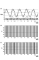
- FIG. 8 is a diagram showing the measurement result of the output waveform in the envelope tracking power supply circuit 5 when the slew rate of the envelope signal S E is low, and I OP is the output current from the voltage follower circuit 7, V C1 , V C2 represents output voltages from the hysteresis comparators 9a and 9b, and I O1 and I O2 represent output currents of the switching converters 11a and 11b, respectively.
- the operation is switched to the operation of only the narrow band / high efficiency power generation unit 19b with a large inductance and a small hysteresis width as time elapses from the start of the operation. At that time, the wideband / low efficiency power generation unit 19b having a small inductance and a large hysteresis width does not operate.
- FIG. 9 is a diagram showing measurement results of output waveforms in the envelope tracking power supply circuit 5 when a high slew rate of the envelope signal S E, in this case the power generating unit 19a is both 19b operate However, the output current is large in the power generation unit 19a having a small inductance and a large hysteresis width.
- the envelope tracking power supply circuit 5 of this embodiment includes two power generation units 19a and 19b, but includes three or more power generation units in which inductance and hysteresis width are changed in multiple stages. Also good.
- the power generation unit 19a, 19b of the present embodiment has a small inductance L 1 is than the inductance L 2, the hysteresis width h 1 is greater than the hysteresis width h 2, it may be set to various inductances and hysteresis widths However, in terms of facilitating the design by adopting the same device for the semiconductor switches 13a, 13b, etc. by bringing the switching frequency closer, the product of the inductance L and the hysteresis width h may be set to be substantially the same. preferable.
- the first and second switching converter units respectively include a first switch and a second switch that are turned on / off according to voltages output from the first and second hysteresis comparator units, and a first switch and a second switch. It is preferable that the first and second inductors that receive a flowing current are included, and the inductance of the first inductor is smaller than the inductance of the second inductor.
- the first switching converter unit has a wider response band to the envelope, while the second switching converter unit has a narrower band to respond to the envelope, but compared to the first switching converter unit.
- Efficiency since the output current is supplied while the first and second switching converter units complement each other in accordance with the slew rate of the envelope, the output current from the voltage follower circuit unit does not increase, and the broadband envelope The overall efficiency can be kept high with respect to the line input.
- the hysteresis width of the first hysteresis comparator unit is larger than the hysteresis width of the second hysteresis comparator unit.
- the switching frequency of the first switching converter unit that operates when the slew rate of the envelope is large and the switching frequency of the second switching converter unit that operates when the slew rate of the envelope is small are obtained. Since they can be close to each other, circuit design can be facilitated by sharing circuit elements constituting the switching converter.
- a high-frequency amplifier includes the envelope tracking power supply circuit described above and an amplifier that amplifies a high-frequency signal upon receiving an output voltage from an output terminal of the envelope tracking power supply circuit. According to such a high-frequency amplifier, the overall efficiency can be maintained high with respect to a high-frequency signal input having a broadband envelope.
- the present invention uses an envelope tracking power supply circuit and a high-frequency amplifier including the same, and maintains high efficiency even for a high-frequency signal having a wide-band envelope.
Landscapes
- Engineering & Computer Science (AREA)
- Power Engineering (AREA)
- Amplifiers (AREA)
- Dc-Dc Converters (AREA)
Priority Applications (3)
| Application Number | Priority Date | Filing Date | Title |
|---|---|---|---|
| US12/866,676 US8587271B2 (en) | 2008-02-08 | 2009-02-03 | Envelope tracking power supply circuit and high-frequency amplifier including envelope tracking power supply circuit |
| EP09707832A EP2244366A1 (en) | 2008-02-08 | 2009-02-03 | Envelope tracking power supply circuit and high-frequency amplifier including envelope tracking power supply circuit |
| CN2009801043868A CN101939900A (zh) | 2008-02-08 | 2009-02-03 | 包络线跟踪电源电路及包括该电路的高频放大器 |
Applications Claiming Priority (2)
| Application Number | Priority Date | Filing Date | Title |
|---|---|---|---|
| JP2008-029333 | 2008-02-08 | ||
| JP2008029333A JP5119961B2 (ja) | 2008-02-08 | 2008-02-08 | 包絡線追跡電源回路及びそれを含む高周波増幅器 |
Publications (1)
| Publication Number | Publication Date |
|---|---|
| WO2009099056A1 true WO2009099056A1 (ja) | 2009-08-13 |
Family
ID=40952131
Family Applications (1)
| Application Number | Title | Priority Date | Filing Date |
|---|---|---|---|
| PCT/JP2009/051771 Ceased WO2009099056A1 (ja) | 2008-02-08 | 2009-02-03 | 包絡線追跡電源回路及びそれを含む高周波増幅器 |
Country Status (6)
| Country | Link |
|---|---|
| US (1) | US8587271B2 (https=) |
| EP (1) | EP2244366A1 (https=) |
| JP (1) | JP5119961B2 (https=) |
| KR (1) | KR20100108561A (https=) |
| CN (1) | CN101939900A (https=) |
| WO (1) | WO2009099056A1 (https=) |
Cited By (3)
| Publication number | Priority date | Publication date | Assignee | Title |
|---|---|---|---|---|
| CN102076139A (zh) * | 2009-11-19 | 2011-05-25 | 群康科技(深圳)有限公司 | Led照明电路 |
| WO2012176578A1 (ja) * | 2011-06-22 | 2012-12-27 | 株式会社村田製作所 | 高周波電力増幅回路用電源装置および高周波電力増幅装置 |
| CN112290898A (zh) * | 2020-09-15 | 2021-01-29 | 复旦大学 | 一种应用于包络跟踪电源调制器的降频采样与控制电路 |
Families Citing this family (87)
| Publication number | Priority date | Publication date | Assignee | Title |
|---|---|---|---|---|
| FI20070672A0 (fi) * | 2007-09-04 | 2007-09-04 | Efore Oyj | Menetelmä vaihtosähkön muodostamiseksi |
| US8995691B2 (en) | 2008-07-14 | 2015-03-31 | Audera Acoustics Inc. | Audio amplifier |
| US9112452B1 (en) | 2009-07-14 | 2015-08-18 | Rf Micro Devices, Inc. | High-efficiency power supply for a modulated load |
| EP2782246B1 (en) | 2010-04-19 | 2018-06-13 | Qorvo US, Inc. | Pseudo-envelope following power management system |
| US9099961B2 (en) | 2010-04-19 | 2015-08-04 | Rf Micro Devices, Inc. | Output impedance compensation of a pseudo-envelope follower power management system |
| US9431974B2 (en) | 2010-04-19 | 2016-08-30 | Qorvo Us, Inc. | Pseudo-envelope following feedback delay compensation |
| US8633766B2 (en) | 2010-04-19 | 2014-01-21 | Rf Micro Devices, Inc. | Pseudo-envelope follower power management system with high frequency ripple current compensation |
| US8981848B2 (en) | 2010-04-19 | 2015-03-17 | Rf Micro Devices, Inc. | Programmable delay circuitry |
| US8519788B2 (en) | 2010-04-19 | 2013-08-27 | Rf Micro Devices, Inc. | Boost charge-pump with fractional ratio and offset loop for supply modulation |
| WO2011145710A1 (ja) | 2010-05-18 | 2011-11-24 | 日本電気株式会社 | 電源装置、およびそれを用いた電力増幅装置 |
| CN101867284B (zh) * | 2010-05-31 | 2012-11-21 | 华为技术有限公司 | 快速跟踪电源的控制方法、快速跟踪电源及系统 |
| US8866549B2 (en) | 2010-06-01 | 2014-10-21 | Rf Micro Devices, Inc. | Method of power amplifier calibration |
| WO2012027039A1 (en) | 2010-08-25 | 2012-03-01 | Rf Micro Devices, Inc. | Multi-mode/multi-band power management system |
| WO2012047738A1 (en) | 2010-09-29 | 2012-04-12 | Rf Micro Devices, Inc. | SINGLE μC-BUCKBOOST CONVERTER WITH MULTIPLE REGULATED SUPPLY OUTPUTS |
| US9075673B2 (en) | 2010-11-16 | 2015-07-07 | Rf Micro Devices, Inc. | Digital fast dB to gain multiplier for envelope tracking systems |
| CN103477557B (zh) * | 2010-12-09 | 2016-07-06 | 射频小型装置公司 | 具有高频波纹电流补偿的伪包络线跟随器功率管理系统 |
| US8588713B2 (en) | 2011-01-10 | 2013-11-19 | Rf Micro Devices, Inc. | Power management system for multi-carriers transmitter |
| US8611402B2 (en) | 2011-02-02 | 2013-12-17 | Rf Micro Devices, Inc. | Fast envelope system calibration |
| US8624760B2 (en) | 2011-02-07 | 2014-01-07 | Rf Micro Devices, Inc. | Apparatuses and methods for rate conversion and fractional delay calculation using a coefficient look up table |
| EP2673880B1 (en) | 2011-02-07 | 2017-09-06 | Qorvo US, Inc. | Group delay calibration method for power amplifier envelope tracking |
| US9054937B2 (en) * | 2011-04-29 | 2015-06-09 | Fairchild Semiconductor Corporation | Envelope extraction with reduced bandwidth for power modulation |
| US9247496B2 (en) | 2011-05-05 | 2016-01-26 | Rf Micro Devices, Inc. | Power loop control based envelope tracking |
| US9379667B2 (en) | 2011-05-05 | 2016-06-28 | Rf Micro Devices, Inc. | Multiple power supply input parallel amplifier based envelope tracking |
| US9246460B2 (en) | 2011-05-05 | 2016-01-26 | Rf Micro Devices, Inc. | Power management architecture for modulated and constant supply operation |
| CN103748794B (zh) | 2011-05-31 | 2015-09-16 | 射频小型装置公司 | 一种用于测量发射路径的复数增益的方法和设备 |
| US9019011B2 (en) | 2011-06-01 | 2015-04-28 | Rf Micro Devices, Inc. | Method of power amplifier calibration for an envelope tracking system |
| US8760228B2 (en) | 2011-06-24 | 2014-06-24 | Rf Micro Devices, Inc. | Differential power management and power amplifier architecture |
| US8952710B2 (en) | 2011-07-15 | 2015-02-10 | Rf Micro Devices, Inc. | Pulsed behavior modeling with steady state average conditions |
| US8626091B2 (en) | 2011-07-15 | 2014-01-07 | Rf Micro Devices, Inc. | Envelope tracking with variable compression |
| WO2013012787A2 (en) | 2011-07-15 | 2013-01-24 | Rf Micro Devices, Inc. | Modified switching ripple for envelope tracking system |
| US9263996B2 (en) | 2011-07-20 | 2016-02-16 | Rf Micro Devices, Inc. | Quasi iso-gain supply voltage function for envelope tracking systems |
| US8618868B2 (en) | 2011-08-17 | 2013-12-31 | Rf Micro Devices, Inc. | Single charge-pump buck-boost for providing independent voltages |
| US8942652B2 (en) | 2011-09-02 | 2015-01-27 | Rf Micro Devices, Inc. | Split VCC and common VCC power management architecture for envelope tracking |
| US8957728B2 (en) | 2011-10-06 | 2015-02-17 | Rf Micro Devices, Inc. | Combined filter and transconductance amplifier |
| US9484797B2 (en) | 2011-10-26 | 2016-11-01 | Qorvo Us, Inc. | RF switching converter with ripple correction |
| CN103988406B (zh) | 2011-10-26 | 2017-03-01 | Qorvo美国公司 | 射频(rf)开关转换器以及使用rf开关转换器的rf放大装置 |
| US9024688B2 (en) | 2011-10-26 | 2015-05-05 | Rf Micro Devices, Inc. | Dual parallel amplifier based DC-DC converter |
| CN103959189B (zh) | 2011-10-26 | 2015-12-23 | 射频小型装置公司 | 基于电感的并行放大器相位补偿 |
| US8975959B2 (en) | 2011-11-30 | 2015-03-10 | Rf Micro Devices, Inc. | Monotonic conversion of RF power amplifier calibration data |
| US9250643B2 (en) | 2011-11-30 | 2016-02-02 | Rf Micro Devices, Inc. | Using a switching signal delay to reduce noise from a switching power supply |
| US9515621B2 (en) | 2011-11-30 | 2016-12-06 | Qorvo Us, Inc. | Multimode RF amplifier system |
| US9041364B2 (en) | 2011-12-01 | 2015-05-26 | Rf Micro Devices, Inc. | RF power converter |
| US9041365B2 (en) | 2011-12-01 | 2015-05-26 | Rf Micro Devices, Inc. | Multiple mode RF power converter |
| US9256234B2 (en) | 2011-12-01 | 2016-02-09 | Rf Micro Devices, Inc. | Voltage offset loop for a switching controller |
| US9280163B2 (en) | 2011-12-01 | 2016-03-08 | Rf Micro Devices, Inc. | Average power tracking controller |
| US8947161B2 (en) | 2011-12-01 | 2015-02-03 | Rf Micro Devices, Inc. | Linear amplifier power supply modulation for envelope tracking |
| US9494962B2 (en) | 2011-12-02 | 2016-11-15 | Rf Micro Devices, Inc. | Phase reconfigurable switching power supply |
| US9813036B2 (en) | 2011-12-16 | 2017-11-07 | Qorvo Us, Inc. | Dynamic loadline power amplifier with baseband linearization |
| US9298198B2 (en) | 2011-12-28 | 2016-03-29 | Rf Micro Devices, Inc. | Noise reduction for envelope tracking |
| CN102624339B (zh) * | 2012-04-10 | 2014-10-15 | 南京航空航天大学 | 一种串联结构包络线跟踪电源及其控制系统 |
| CN102624231A (zh) * | 2012-04-10 | 2012-08-01 | 南京航空航天大学 | 一种并联结构包络线跟踪电源 |
| US8816768B2 (en) | 2012-04-12 | 2014-08-26 | Mediatek Inc. | Power module for envelope tracking |
| US9071200B2 (en) | 2012-04-12 | 2015-06-30 | Mediatek Inc. | Power module for envelope tracking |
| WO2013168598A1 (ja) * | 2012-05-08 | 2013-11-14 | 株式会社村田製作所 | 高周波電力増幅回路用電源装置および高周波電力増幅装置 |
| US8981839B2 (en) | 2012-06-11 | 2015-03-17 | Rf Micro Devices, Inc. | Power source multiplexer |
| WO2014018861A1 (en) | 2012-07-26 | 2014-01-30 | Rf Micro Devices, Inc. | Programmable rf notch filter for envelope tracking |
| US8779860B2 (en) | 2012-08-15 | 2014-07-15 | Avago Technologies General Ip (Singapore) Ptd. Ltd. | Power amplifier |
| US9225231B2 (en) | 2012-09-14 | 2015-12-29 | Rf Micro Devices, Inc. | Open loop ripple cancellation circuit in a DC-DC converter |
| US9197256B2 (en) | 2012-10-08 | 2015-11-24 | Rf Micro Devices, Inc. | Reducing effects of RF mixer-based artifact using pre-distortion of an envelope power supply signal |
| US9207692B2 (en) | 2012-10-18 | 2015-12-08 | Rf Micro Devices, Inc. | Transitioning from envelope tracking to average power tracking |
| CN103812334A (zh) * | 2012-11-14 | 2014-05-21 | 立锜科技股份有限公司 | 多输出切换式电源供应器及多输出电源供应方法 |
| US9627975B2 (en) | 2012-11-16 | 2017-04-18 | Qorvo Us, Inc. | Modulated power supply system and method with automatic transition between buck and boost modes |
| WO2014116933A2 (en) | 2013-01-24 | 2014-07-31 | Rf Micro Devices, Inc | Communications based adjustments of an envelope tracking power supply |
| US9178472B2 (en) | 2013-02-08 | 2015-11-03 | Rf Micro Devices, Inc. | Bi-directional power supply signal based linear amplifier |
| US9608675B2 (en) | 2013-02-11 | 2017-03-28 | Qualcomm Incorporated | Power tracker for multiple transmit signals sent simultaneously |
| WO2014152876A1 (en) | 2013-03-14 | 2014-09-25 | Rf Micro Devices, Inc | Noise conversion gain limited rf power amplifier |
| US9197162B2 (en) | 2013-03-14 | 2015-11-24 | Rf Micro Devices, Inc. | Envelope tracking power supply voltage dynamic range reduction |
| US9479118B2 (en) | 2013-04-16 | 2016-10-25 | Rf Micro Devices, Inc. | Dual instantaneous envelope tracking |
| US9374005B2 (en) | 2013-08-13 | 2016-06-21 | Rf Micro Devices, Inc. | Expanded range DC-DC converter |
| KR102114726B1 (ko) * | 2013-10-23 | 2020-06-05 | 삼성전자주식회사 | 전력 증폭 장치 및 방법 |
| CN103701089A (zh) * | 2013-12-31 | 2014-04-02 | 昌辉汽车转向系统(黄山)有限公司 | 一种硬件过载或短路保护电路及dc电源供电电路 |
| US9473089B2 (en) | 2014-05-08 | 2016-10-18 | Mediatek Inc. | Hybrid power module |
| US9614476B2 (en) | 2014-07-01 | 2017-04-04 | Qorvo Us, Inc. | Group delay calibration of RF envelope tracking |
| CN105981450B (zh) * | 2014-07-30 | 2020-04-14 | 华为技术有限公司 | 功率放大器的供电电压控制方法及电子设备 |
| US9685864B2 (en) * | 2015-03-31 | 2017-06-20 | Qualcomm Incorporated | Switching regulator circuits and methods with reconfigurable inductance |
| US9748901B2 (en) | 2015-06-16 | 2017-08-29 | Avago Technologies General Ip (Singapore) Pte. Ltd. | Power amplifying apparatus |
| US9912297B2 (en) | 2015-07-01 | 2018-03-06 | Qorvo Us, Inc. | Envelope tracking power converter circuitry |
| US9843294B2 (en) | 2015-07-01 | 2017-12-12 | Qorvo Us, Inc. | Dual-mode envelope tracking power converter circuitry |
| US9973147B2 (en) | 2016-05-10 | 2018-05-15 | Qorvo Us, Inc. | Envelope tracking power management circuit |
| CN105896983A (zh) * | 2016-05-13 | 2016-08-24 | 南京航空航天大学 | 宽频带输出的包络线跟踪电源 |
| US10411706B1 (en) | 2017-10-20 | 2019-09-10 | United States Of America As Represented By The Secretary Of The Air Force | Wide-band digital buffer driver |
| US10476437B2 (en) | 2018-03-15 | 2019-11-12 | Qorvo Us, Inc. | Multimode voltage tracker circuit |
| US10826439B2 (en) | 2018-12-18 | 2020-11-03 | Nxp Usa, Inc. | Linearity enhancement of high power amplifiers |
| CN110635667B (zh) * | 2019-09-03 | 2021-09-24 | 电子科技大学 | 一种用于包络跟踪系统的三电平滞回控制电源调制器 |
| US11420524B2 (en) * | 2019-12-20 | 2022-08-23 | Ut-Battelle, Llc | Wireless power system |
| KR102868054B1 (ko) | 2021-01-14 | 2025-10-01 | 삼성전자주식회사 | 전원 변조기 및 이를 포함하는 무선 통신 장치 |
| CN112838748B (zh) * | 2021-01-27 | 2022-04-12 | 陕西亚成微电子股份有限公司 | 一种包络追踪电源的控制方法及电路 |
Citations (2)
| Publication number | Priority date | Publication date | Assignee | Title |
|---|---|---|---|---|
| JP2003533116A (ja) * | 2000-05-05 | 2003-11-05 | テレフオンアクチーボラゲツト エル エム エリクソン(パブル) | 広帯域包絡線信号を効率的に増幅する装置と方法 |
| JP2007531488A (ja) * | 2004-03-31 | 2007-11-01 | コーニンクレッカ フィリップス エレクトロニクス エヌ ヴィ | 並列に配置した電源 |
Family Cites Families (6)
| Publication number | Priority date | Publication date | Assignee | Title |
|---|---|---|---|---|
| JPH03201818A (ja) * | 1989-12-28 | 1991-09-03 | Fujitsu Ltd | 比較回路 |
| US5905407A (en) | 1997-07-30 | 1999-05-18 | Motorola, Inc. | High efficiency power amplifier using combined linear and switching techniques with novel feedback system |
| US6565001B1 (en) * | 2001-11-08 | 2003-05-20 | Em Microelectronics-Us, Inc | Receiver circuit and method for a contactless identification system |
| JP2009200944A (ja) * | 2008-02-22 | 2009-09-03 | Oki Semiconductor Co Ltd | ヒステリシスコンパレータ |
| US7808323B2 (en) * | 2008-05-23 | 2010-10-05 | Panasonic Corporation | High-efficiency envelope tracking systems and methods for radio frequency power amplifiers |
| US8030995B2 (en) * | 2008-12-25 | 2011-10-04 | Hitachi Kokusai Electric Inc. | Power circuit used for an amplifier |
-
2008
- 2008-02-08 JP JP2008029333A patent/JP5119961B2/ja not_active Expired - Fee Related
-
2009
- 2009-02-03 US US12/866,676 patent/US8587271B2/en not_active Expired - Fee Related
- 2009-02-03 CN CN2009801043868A patent/CN101939900A/zh active Pending
- 2009-02-03 EP EP09707832A patent/EP2244366A1/en not_active Withdrawn
- 2009-02-03 KR KR1020107015825A patent/KR20100108561A/ko not_active Ceased
- 2009-02-03 WO PCT/JP2009/051771 patent/WO2009099056A1/ja not_active Ceased
Patent Citations (2)
| Publication number | Priority date | Publication date | Assignee | Title |
|---|---|---|---|---|
| JP2003533116A (ja) * | 2000-05-05 | 2003-11-05 | テレフオンアクチーボラゲツト エル エム エリクソン(パブル) | 広帯域包絡線信号を効率的に増幅する装置と方法 |
| JP2007531488A (ja) * | 2004-03-31 | 2007-11-01 | コーニンクレッカ フィリップス エレクトロニクス エヌ ヴィ | 並列に配置した電源 |
Non-Patent Citations (4)
| Title |
|---|
| D. F. KIMBALL ET AL.: "High-Efficiency Envelope-Tracking W-CDMA Base-Station Amplifier Using GaN HFETs", IEEE TRANS. ON MICROWAVE THEORY AND TECHNIQUES, vol. 54, no. 11, November 2006 (2006-11-01) |
| F. WANG: "High Efficiency Linear Envelope Tracking and Envelope Elimination and Restoration Power Amplifier for WLAN OFDM Applications", PH.D. DISSERTATION, 2006 |
| P. ASBECK; D. KIMBALL ET AL.: "Next Genaration High-Efficiency RF Transmitter Technology for Basestations", EXTENDED ABSTRACTS OF 2007 INTERNATIONAL CONFERENCE ON SOLID SATE DEVICES AND MATERIALS, September 2007 (2007-09-01), pages 146 - 147 |
| P. DRAXLER; S. LANFRANCO ET AL.: "High Efficiency Envelope Tracking LDMOS Power Amplifier for W-CDMA", IEEE MTT-S INTERNATIONAL MICROWAVE SYMPOSIUM, June 2006 (2006-06-01), pages 1534 - 1537 |
Cited By (6)
| Publication number | Priority date | Publication date | Assignee | Title |
|---|---|---|---|---|
| CN102076139A (zh) * | 2009-11-19 | 2011-05-25 | 群康科技(深圳)有限公司 | Led照明电路 |
| WO2012176578A1 (ja) * | 2011-06-22 | 2012-12-27 | 株式会社村田製作所 | 高周波電力増幅回路用電源装置および高周波電力増幅装置 |
| JPWO2012176578A1 (ja) * | 2011-06-22 | 2015-02-23 | 株式会社村田製作所 | 高周波電力増幅回路用電源装置および高周波電力増幅装置 |
| US9148090B2 (en) | 2011-06-22 | 2015-09-29 | Murata Manufacturing Co., Ltd. | Power supply device for high frequency power amplification circuit and high frequency power amplification device |
| CN112290898A (zh) * | 2020-09-15 | 2021-01-29 | 复旦大学 | 一种应用于包络跟踪电源调制器的降频采样与控制电路 |
| CN112290898B (zh) * | 2020-09-15 | 2022-12-20 | 复旦大学 | 一种应用于包络跟踪电源调制器的降频采样与控制电路 |
Also Published As
| Publication number | Publication date |
|---|---|
| JP5119961B2 (ja) | 2013-01-16 |
| JP2009189215A (ja) | 2009-08-20 |
| KR20100108561A (ko) | 2010-10-07 |
| CN101939900A (zh) | 2011-01-05 |
| EP2244366A1 (en) | 2010-10-27 |
| US20110031953A1 (en) | 2011-02-10 |
| US8587271B2 (en) | 2013-11-19 |
Similar Documents
| Publication | Publication Date | Title |
|---|---|---|
| JP5119961B2 (ja) | 包絡線追跡電源回路及びそれを含む高周波増幅器 | |
| KR101467231B1 (ko) | 포락선 추적 모드 또는 평균 전력 추적 모드로 동작하는 멀티 모드 바이어스 변조기 및 이를 이용한 포락선 추적 전력 증폭 장치 | |
| US7949316B2 (en) | High-efficiency envelope tracking systems and methods for radio frequency power amplifiers | |
| US9590563B2 (en) | 2G support for 2G and 3G/4G envelope tracking modulator | |
| JP6571071B2 (ja) | 可変ブースト電源電圧を用いたエンベロープトラッカー | |
| US9491314B2 (en) | Voltage boost for ET modulator | |
| US7808323B2 (en) | High-efficiency envelope tracking systems and methods for radio frequency power amplifiers | |
| US9559637B2 (en) | Multi-mode bias modulator and envelope tracking power amplifier using the same | |
| JP2010166157A (ja) | 包絡線追跡電源回路及び増幅装置 | |
| US9270241B2 (en) | Power supply device, transmission device using same, and method for operating power supply device | |
| KR101664718B1 (ko) | 이중 구동 전압을 이용하는 평균 전력 추적 모드 전력 증폭 장치 | |
| JP2008035487A (ja) | Rf電力増幅器 | |
| US9602070B2 (en) | Power amplifying device | |
| CN102265504A (zh) | 功率放大装置 | |
| EP2602932A1 (en) | Power modulator, and method for controlling same | |
| CN112585867B (zh) | 用于辅助功率放大器的电源电压中具有瞬态响应的包络跟踪的装置和方法 | |
| Kanbe et al. | New architecture for envelope-tracking power amplifier for base station | |
| US9577583B2 (en) | Power amplifier | |
| Xiong et al. | A highly-applicable supply modulator with a highly-linear envelope detector for WCDMA envelope-tracking applications | |
| US10158331B2 (en) | Power amplifying apparatus with boost function | |
| Son et al. | A hybrid envelope amplifier with switching-controlled structure for EDGE/WCDMA/LTE reconfigurable transmitters | |
| Bae et al. | CMOS dynamic supply switching power amplifier for LTE applications | |
| Kaneta et al. | Architecture of wideband high-efficiency envelope tracking power amplifier for base station | |
| JP2012023489A (ja) | 変調電源 | |
| JP2012129787A (ja) | 電源回路 |
Legal Events
| Date | Code | Title | Description |
|---|---|---|---|
| WWE | Wipo information: entry into national phase |
Ref document number: 200980104386.8 Country of ref document: CN |
|
| 121 | Ep: the epo has been informed by wipo that ep was designated in this application |
Ref document number: 09707832 Country of ref document: EP Kind code of ref document: A1 |
|
| ENP | Entry into the national phase |
Ref document number: 20107015825 Country of ref document: KR Kind code of ref document: A |
|
| NENP | Non-entry into the national phase |
Ref country code: DE |
|
| WWE | Wipo information: entry into national phase |
Ref document number: 2009707832 Country of ref document: EP |
|
| WWE | Wipo information: entry into national phase |
Ref document number: 12866676 Country of ref document: US |