WO2006038020A1 - Light emitting device - Google Patents
Light emitting device Download PDFInfo
- Publication number
- WO2006038020A1 WO2006038020A1 PCT/GB2005/003864 GB2005003864W WO2006038020A1 WO 2006038020 A1 WO2006038020 A1 WO 2006038020A1 GB 2005003864 W GB2005003864 W GB 2005003864W WO 2006038020 A1 WO2006038020 A1 WO 2006038020A1
- Authority
- WO
- WIPO (PCT)
- Prior art keywords
- layer
- phosphorescent
- exciton generating
- generating layer
- singlet
- Prior art date
Links
- 239000011368 organic material Substances 0.000 claims abstract description 19
- 239000000463 material Substances 0.000 claims description 60
- 230000000903 blocking effect Effects 0.000 claims description 21
- 238000005286 illumination Methods 0.000 claims description 7
- 229920000642 polymer Polymers 0.000 claims description 7
- 230000005525 hole transport Effects 0.000 claims description 6
- 150000004696 coordination complex Chemical class 0.000 claims description 4
- PJANXHGTPQOBST-VAWYXSNFSA-N Stilbene Natural products C=1C=CC=CC=1/C=C/C1=CC=CC=C1 PJANXHGTPQOBST-VAWYXSNFSA-N 0.000 claims description 2
- PJANXHGTPQOBST-UHFFFAOYSA-N stilbene Chemical compound C=1C=CC=CC=1C=CC1=CC=CC=C1 PJANXHGTPQOBST-UHFFFAOYSA-N 0.000 claims description 2
- 235000021286 stilbenes Nutrition 0.000 claims description 2
- 229920000620 organic polymer Polymers 0.000 claims 1
- 239000010410 layer Substances 0.000 description 127
- 238000010129 solution processing Methods 0.000 description 12
- 238000000034 method Methods 0.000 description 10
- 238000004519 manufacturing process Methods 0.000 description 7
- CUJRVFIICFDLGR-UHFFFAOYSA-N acetylacetonate Chemical compound CC(=O)[CH-]C(C)=O CUJRVFIICFDLGR-UHFFFAOYSA-N 0.000 description 6
- 239000003446 ligand Substances 0.000 description 6
- 229910052751 metal Inorganic materials 0.000 description 6
- 239000002184 metal Substances 0.000 description 6
- 239000000243 solution Substances 0.000 description 6
- IJGRMHOSHXDMSA-UHFFFAOYSA-N Atomic nitrogen Chemical compound N#N IJGRMHOSHXDMSA-UHFFFAOYSA-N 0.000 description 5
- 239000000412 dendrimer Substances 0.000 description 5
- 238000009792 diffusion process Methods 0.000 description 5
- 238000006243 chemical reaction Methods 0.000 description 4
- 238000000151 deposition Methods 0.000 description 4
- 239000002019 doping agent Substances 0.000 description 4
- 238000004768 lowest unoccupied molecular orbital Methods 0.000 description 4
- 238000005215 recombination Methods 0.000 description 4
- 230000006798 recombination Effects 0.000 description 4
- 238000001228 spectrum Methods 0.000 description 4
- OKTJSMMVPCPJKN-UHFFFAOYSA-N Carbon Chemical compound [C] OKTJSMMVPCPJKN-UHFFFAOYSA-N 0.000 description 3
- 229920000144 PEDOT:PSS Polymers 0.000 description 3
- 229920001609 Poly(3,4-ethylenedioxythiophene) Polymers 0.000 description 3
- 125000000217 alkyl group Chemical group 0.000 description 3
- 239000004411 aluminium Substances 0.000 description 3
- 229910052782 aluminium Inorganic materials 0.000 description 3
- XAGFODPZIPBFFR-UHFFFAOYSA-N aluminium Chemical compound [Al] XAGFODPZIPBFFR-UHFFFAOYSA-N 0.000 description 3
- 125000000732 arylene group Chemical group 0.000 description 3
- 230000008901 benefit Effects 0.000 description 3
- 229910052799 carbon Inorganic materials 0.000 description 3
- 239000003086 colorant Substances 0.000 description 3
- 150000001875 compounds Chemical class 0.000 description 3
- 238000003306 harvesting Methods 0.000 description 3
- 239000000203 mixture Substances 0.000 description 3
- 229910052757 nitrogen Inorganic materials 0.000 description 3
- 229920001467 poly(styrenesulfonates) Polymers 0.000 description 3
- 238000004528 spin coating Methods 0.000 description 3
- 125000001424 substituent group Chemical group 0.000 description 3
- 239000000758 substrate Substances 0.000 description 3
- UJOBWOGCFQCDNV-UHFFFAOYSA-N 9H-carbazole Chemical compound C1=CC=C2C3=CC=CC=C3NC2=C1 UJOBWOGCFQCDNV-UHFFFAOYSA-N 0.000 description 2
- KDLHZDBZIXYQEI-UHFFFAOYSA-N Palladium Chemical compound [Pd] KDLHZDBZIXYQEI-UHFFFAOYSA-N 0.000 description 2
- OAICVXFJPJFONN-UHFFFAOYSA-N Phosphorus Chemical compound [P] OAICVXFJPJFONN-UHFFFAOYSA-N 0.000 description 2
- -1 Poly(ethylene dioxythiophene) Polymers 0.000 description 2
- JUJWROOIHBZHMG-UHFFFAOYSA-N Pyridine Chemical compound C1=CC=NC=C1 JUJWROOIHBZHMG-UHFFFAOYSA-N 0.000 description 2
- 230000032683 aging Effects 0.000 description 2
- 125000003545 alkoxy group Chemical group 0.000 description 2
- 238000013459 approach Methods 0.000 description 2
- 230000015572 biosynthetic process Effects 0.000 description 2
- 239000002322 conducting polymer Substances 0.000 description 2
- 229920001940 conductive polymer Polymers 0.000 description 2
- 229920000736 dendritic polymer Polymers 0.000 description 2
- 230000008021 deposition Effects 0.000 description 2
- 239000000975 dye Substances 0.000 description 2
- 230000005281 excited state Effects 0.000 description 2
- 239000011521 glass Substances 0.000 description 2
- 125000001072 heteroaryl group Chemical group 0.000 description 2
- AMGQUBHHOARCQH-UHFFFAOYSA-N indium;oxotin Chemical compound [In].[Sn]=O AMGQUBHHOARCQH-UHFFFAOYSA-N 0.000 description 2
- BASFCYQUMIYNBI-UHFFFAOYSA-N platinum Chemical compound [Pt] BASFCYQUMIYNBI-UHFFFAOYSA-N 0.000 description 2
- 238000010791 quenching Methods 0.000 description 2
- 230000000171 quenching effect Effects 0.000 description 2
- 230000005855 radiation Effects 0.000 description 2
- 125000005259 triarylamine group Chemical group 0.000 description 2
- POILWHVDKZOXJZ-ARJAWSKDSA-M (z)-4-oxopent-2-en-2-olate Chemical compound C\C([O-])=C\C(C)=O POILWHVDKZOXJZ-ARJAWSKDSA-M 0.000 description 1
- SNTWKPAKVQFCCF-UHFFFAOYSA-N 2,3-dihydro-1h-triazole Chemical compound N1NC=CN1 SNTWKPAKVQFCCF-UHFFFAOYSA-N 0.000 description 1
- STTGYIUESPWXOW-UHFFFAOYSA-N 2,9-dimethyl-4,7-diphenyl-1,10-phenanthroline Chemical compound C=12C=CC3=C(C=4C=CC=CC=4)C=C(C)N=C3C2=NC(C)=CC=1C1=CC=CC=C1 STTGYIUESPWXOW-UHFFFAOYSA-N 0.000 description 1
- ZCYVEMRRCGMTRW-UHFFFAOYSA-N 7553-56-2 Chemical compound [I] ZCYVEMRRCGMTRW-UHFFFAOYSA-N 0.000 description 1
- 239000005725 8-Hydroxyquinoline Substances 0.000 description 1
- WKBOTKDWSSQWDR-UHFFFAOYSA-N Bromine atom Chemical compound [Br] WKBOTKDWSSQWDR-UHFFFAOYSA-N 0.000 description 1
- OYPRJOBELJOOCE-UHFFFAOYSA-N Calcium Chemical compound [Ca] OYPRJOBELJOOCE-UHFFFAOYSA-N 0.000 description 1
- ZAMOUSCENKQFHK-UHFFFAOYSA-N Chlorine atom Chemical compound [Cl] ZAMOUSCENKQFHK-UHFFFAOYSA-N 0.000 description 1
- PXGOKWXKJXAPGV-UHFFFAOYSA-N Fluorine Chemical compound FF PXGOKWXKJXAPGV-UHFFFAOYSA-N 0.000 description 1
- CTQNGGLPUBDAKN-UHFFFAOYSA-N O-Xylene Chemical compound CC1=CC=CC=C1C CTQNGGLPUBDAKN-UHFFFAOYSA-N 0.000 description 1
- KJTLSVCANCCWHF-UHFFFAOYSA-N Ruthenium Chemical compound [Ru] KJTLSVCANCCWHF-UHFFFAOYSA-N 0.000 description 1
- 239000007983 Tris buffer Substances 0.000 description 1
- 238000004026 adhesive bonding Methods 0.000 description 1
- 125000002877 alkyl aryl group Chemical group 0.000 description 1
- 125000003710 aryl alkyl group Chemical group 0.000 description 1
- 125000003118 aryl group Chemical group 0.000 description 1
- 229910052788 barium Inorganic materials 0.000 description 1
- DSAJWYNOEDNPEQ-UHFFFAOYSA-N barium atom Chemical compound [Ba] DSAJWYNOEDNPEQ-UHFFFAOYSA-N 0.000 description 1
- GDTBXPJZTBHREO-UHFFFAOYSA-N bromine Substances BrBr GDTBXPJZTBHREO-UHFFFAOYSA-N 0.000 description 1
- 229910052794 bromium Inorganic materials 0.000 description 1
- 229910052791 calcium Inorganic materials 0.000 description 1
- 239000011575 calcium Substances 0.000 description 1
- 230000008859 change Effects 0.000 description 1
- 229910052801 chlorine Inorganic materials 0.000 description 1
- 239000000460 chlorine Substances 0.000 description 1
- 229920000547 conjugated polymer Polymers 0.000 description 1
- 229920001577 copolymer Polymers 0.000 description 1
- 230000008878 coupling Effects 0.000 description 1
- 238000010168 coupling process Methods 0.000 description 1
- 238000005859 coupling reaction Methods 0.000 description 1
- 125000004093 cyano group Chemical group *C#N 0.000 description 1
- 238000005401 electroluminescence Methods 0.000 description 1
- 238000005516 engineering process Methods 0.000 description 1
- 238000001704 evaporation Methods 0.000 description 1
- 230000008020 evaporation Effects 0.000 description 1
- 125000003983 fluorenyl group Chemical class C1(=CC=CC=2C3=CC=CC=C3CC12)* 0.000 description 1
- 229910052731 fluorine Inorganic materials 0.000 description 1
- 239000011737 fluorine Substances 0.000 description 1
- PCHJSUWPFVWCPO-UHFFFAOYSA-N gold Chemical compound [Au] PCHJSUWPFVWCPO-UHFFFAOYSA-N 0.000 description 1
- 229910052737 gold Inorganic materials 0.000 description 1
- 239000010931 gold Substances 0.000 description 1
- 230000005283 ground state Effects 0.000 description 1
- 229910001385 heavy metal Inorganic materials 0.000 description 1
- 230000006872 improvement Effects 0.000 description 1
- 238000010348 incorporation Methods 0.000 description 1
- PJULCNAVAGQLAT-UHFFFAOYSA-N indeno[2,1-a]fluorene Chemical compound C1=CC=C2C=C3C4=CC5=CC=CC=C5C4=CC=C3C2=C1 PJULCNAVAGQLAT-UHFFFAOYSA-N 0.000 description 1
- 238000007641 inkjet printing Methods 0.000 description 1
- 229910052740 iodine Inorganic materials 0.000 description 1
- 239000011630 iodine Substances 0.000 description 1
- 229910052741 iridium Inorganic materials 0.000 description 1
- GKOZUEZYRPOHIO-UHFFFAOYSA-N iridium atom Chemical compound [Ir] GKOZUEZYRPOHIO-UHFFFAOYSA-N 0.000 description 1
- 239000004973 liquid crystal related substance Substances 0.000 description 1
- 238000004020 luminiscence type Methods 0.000 description 1
- QSHDDOUJBYECFT-UHFFFAOYSA-N mercury Chemical compound [Hg] QSHDDOUJBYECFT-UHFFFAOYSA-N 0.000 description 1
- 229910052753 mercury Inorganic materials 0.000 description 1
- 229910001512 metal fluoride Inorganic materials 0.000 description 1
- 229910044991 metal oxide Inorganic materials 0.000 description 1
- 150000002739 metals Chemical class 0.000 description 1
- 238000002156 mixing Methods 0.000 description 1
- QJGQUHMNIGDVPM-UHFFFAOYSA-N nitrogen group Chemical group [N] QJGQUHMNIGDVPM-UHFFFAOYSA-N 0.000 description 1
- NIHNNTQXNPWCJQ-UHFFFAOYSA-N o-biphenylenemethane Natural products C1=CC=C2CC3=CC=CC=C3C2=C1 NIHNNTQXNPWCJQ-UHFFFAOYSA-N 0.000 description 1
- 229910052762 osmium Inorganic materials 0.000 description 1
- SYQBFIAQOQZEGI-UHFFFAOYSA-N osmium atom Chemical compound [Os] SYQBFIAQOQZEGI-UHFFFAOYSA-N 0.000 description 1
- WCPAKWJPBJAGKN-UHFFFAOYSA-N oxadiazole Chemical compound C1=CON=N1 WCPAKWJPBJAGKN-UHFFFAOYSA-N 0.000 description 1
- 229960003540 oxyquinoline Drugs 0.000 description 1
- 229910052763 palladium Inorganic materials 0.000 description 1
- 125000005010 perfluoroalkyl group Chemical group 0.000 description 1
- 125000000843 phenylene group Chemical group C1(=C(C=CC=C1)*)* 0.000 description 1
- 229910052697 platinum Inorganic materials 0.000 description 1
- 229920002959 polymer blend Polymers 0.000 description 1
- 150000004032 porphyrins Chemical class 0.000 description 1
- 239000002243 precursor Substances 0.000 description 1
- UMJSCPRVCHMLSP-UHFFFAOYSA-N pyridine Natural products COC1=CC=CN=C1 UMJSCPRVCHMLSP-UHFFFAOYSA-N 0.000 description 1
- MCJGNVYPOGVAJF-UHFFFAOYSA-N quinolin-8-ol Chemical compound C1=CN=C2C(O)=CC=CC2=C1 MCJGNVYPOGVAJF-UHFFFAOYSA-N 0.000 description 1
- 238000009877 rendering Methods 0.000 description 1
- 229910052702 rhenium Inorganic materials 0.000 description 1
- WUAPFZMCVAUBPE-UHFFFAOYSA-N rhenium atom Chemical compound [Re] WUAPFZMCVAUBPE-UHFFFAOYSA-N 0.000 description 1
- 229910052703 rhodium Inorganic materials 0.000 description 1
- 239000010948 rhodium Substances 0.000 description 1
- MHOVAHRLVXNVSD-UHFFFAOYSA-N rhodium atom Chemical compound [Rh] MHOVAHRLVXNVSD-UHFFFAOYSA-N 0.000 description 1
- 229910052707 ruthenium Inorganic materials 0.000 description 1
- 239000002356 single layer Substances 0.000 description 1
- 150000003384 small molecules Chemical class 0.000 description 1
- 239000002904 solvent Substances 0.000 description 1
- 239000000126 substance Substances 0.000 description 1
- 125000003107 substituted aryl group Chemical group 0.000 description 1
- 125000004001 thioalkyl group Chemical group 0.000 description 1
- 150000003852 triazoles Chemical class 0.000 description 1
- 125000002023 trifluoromethyl group Chemical group FC(F)(F)* 0.000 description 1
- 238000007738 vacuum evaporation Methods 0.000 description 1
- 238000001429 visible spectrum Methods 0.000 description 1
- 239000008096 xylene Substances 0.000 description 1
Classifications
-
- H—ELECTRICITY
- H10—SEMICONDUCTOR DEVICES; ELECTRIC SOLID-STATE DEVICES NOT OTHERWISE PROVIDED FOR
- H10K—ORGANIC ELECTRIC SOLID-STATE DEVICES
- H10K50/00—Organic light-emitting devices
- H10K50/10—OLEDs or polymer light-emitting diodes [PLED]
- H10K50/11—OLEDs or polymer light-emitting diodes [PLED] characterised by the electroluminescent [EL] layers
- H10K50/125—OLEDs or polymer light-emitting diodes [PLED] characterised by the electroluminescent [EL] layers specially adapted for multicolour light emission, e.g. for emitting white light
-
- H—ELECTRICITY
- H10—SEMICONDUCTOR DEVICES; ELECTRIC SOLID-STATE DEVICES NOT OTHERWISE PROVIDED FOR
- H10K—ORGANIC ELECTRIC SOLID-STATE DEVICES
- H10K2101/00—Properties of the organic materials covered by group H10K85/00
- H10K2101/10—Triplet emission
-
- H—ELECTRICITY
- H10—SEMICONDUCTOR DEVICES; ELECTRIC SOLID-STATE DEVICES NOT OTHERWISE PROVIDED FOR
- H10K—ORGANIC ELECTRIC SOLID-STATE DEVICES
- H10K50/00—Organic light-emitting devices
- H10K50/10—OLEDs or polymer light-emitting diodes [PLED]
- H10K50/18—Carrier blocking layers
-
- H—ELECTRICITY
- H10—SEMICONDUCTOR DEVICES; ELECTRIC SOLID-STATE DEVICES NOT OTHERWISE PROVIDED FOR
- H10K—ORGANIC ELECTRIC SOLID-STATE DEVICES
- H10K85/00—Organic materials used in the body or electrodes of devices covered by this subclass
- H10K85/10—Organic polymers or oligomers
- H10K85/111—Organic polymers or oligomers comprising aromatic, heteroaromatic, or aryl chains, e.g. polyaniline, polyphenylene or polyphenylene vinylene
- H10K85/115—Polyfluorene; Derivatives thereof
-
- H—ELECTRICITY
- H10—SEMICONDUCTOR DEVICES; ELECTRIC SOLID-STATE DEVICES NOT OTHERWISE PROVIDED FOR
- H10K—ORGANIC ELECTRIC SOLID-STATE DEVICES
- H10K85/00—Organic materials used in the body or electrodes of devices covered by this subclass
- H10K85/10—Organic polymers or oligomers
- H10K85/151—Copolymers
Definitions
- Luminescent conjugated polymers are a new technologically important class of materials that will be used in light emitting display devices for the next generation of information technology based consumer products.
- OLEDs organic light emitting diodes
- the standard fluorescent tube is an example of the use of down-conversion to generate illumination-quality white light.
- the source of the photons is a mercury discharge, giving mainly blue light.
- Phosphors on the surface of the glass tube convert some of these photons to the yellow area of the spectrum and the combination of blue plus yellow is perceived as white.
- the fluorescent tubes can not be used in flat panel displays and so more recent OLEDs represent a significant advantage over these.
- Applied Physics Letters 80(19), 3470-3472, 2002 discloses another approach; using an organic light emitting polymer device comprising an electroluminescent material that emits blue fluorescence. Phosphors or dyes external to the organic device absorb some of the "blue" photons and re-emit photons of lower energy, thereby "down converting" some of the blue emission to yellow. The blue and yellow emissions combine to form white emission.
- the blue electroluminescent material of this device generates both singlet and triplet excitons.
- all emission in this device i.e. blue and downconverted yellow
- the blue emission of the electroluminescent material which in turn is derived from singlet excitons, i.e. the triplets excitons generated by the blue electroluminescent material are not harvested.
- the ratio of singlet excitons to triplet excitons can be as high as 1:3 (as discussed in, for example, Chem. Phys. Lett., 1993, 210, 61, Nature (London), 2001, 409, 494, Synth. Met., 2002, 125, 55 and references therein) . Consequently, the theoretical maximum efficiency of this device may be as low as 25%.
- white phosphorescent device is disclosed in Advanced Materials, 2002, 14, No. 2, "Controlling Exciton Diffusion in Multilayer White Phosphorescent Organic Light Emitting Devices".
- This disclosure is concerned with a white organic light emitting device.
- white organic light emitting devices WOLEDs
- WOLEDs white organic light emitting devices
- white light emission can be obtained from multilayer OLED structures in which different layers emit different parts of the visible spectrum, from single layer polymer blends, or from hybrid organic/inorganic structures, white light-emitting materials, or exciplexes.
- the compounds FIrpic and Bt 2 Ir emit by absorbing singlet and triplet excitons and emitting from a triplet molecular excited state (phosphorescence) .
- These phosphorescent devices have higher efficiency than the aforementioned fluorescent device as a result of triplet excitons being harvested.
- these devices suffer from two drawbacks. Firstly, the blue emission from a phosphorescent compound requires a high triplet energy level and a yet higher triplet energy level dopant. These are particularly demanding requirements and in consequence blue emission from FIrpic is relatively poor as compared to blue as defined by 1931 CIE co-ordinates. Secondly, the colours of the two emissive species change over device lifetime and in consequence colour stability of these devices is a problem.
- triplets have lifetimes that are several orders of magnitude longer than singlets, hence they have longer diffusion lengths, allowing emissive layers to be >10 nm thick.
- Advanced Materials 2002, 14, No. 2 teaches that the CIE coordinates of the OLED emission can be tuned over a wide range.
- the blocker is a thin BCP, hole/exciton blocking layer placed between the FIrpic and Btp 2 lr(acac) doped layers. It is said that this layer retards the flow of holes from the FIrpic doped layer towards the cathode and thereby forces more excitons to form in the FIrpic layer, and it prevents excitons from diffusing towards the cathode after forming in the FIrpic doped layer.
- the host-dopant systems used in the emissive regions in device 1 and device 2 in Advanced Materials 2002, 14, No. 2 are not solution processable. Further, the blue EMR does not give blue light with adequate colour and efficiency to exceed the performance of white devices based on fluorescent blue plus external down-conversion. In view of the above, it will be appreciated that there exists a need to provide an efficient white organic light-emitting device (WOLED), which preferably is solution processable.
- WOLED white organic light-emitting device
- the present invention at least partially addresses this need by providing a light-emitting device comprising an anode; a cathode; and a light emitting region situated between the anode and the cathode, said light emitting region comprising an exciton generating layer and a phosphorescent layer, the exciton generating layer comprising an organic material, wherein the organic material of the exciton generating layer generates singlet and triplet excitons and emits light by- fluorescent emission from the singlet excitons and the phosphorescent layer accepts the triplet excitons from the exciton generating layer and emits light by phosphorescent emission from the triplet excitons.
- singlet and triplet excitons are generated from a single source; the organic material of the exciton generating layer.
- the singlet excitons decay to generate light from a different material than the triplet excitons.
- light is generated from two sources; the organic material of the exciton generating layer, which harvests the singlet excitons, and the phosphorescent layer, which harvests the triplet excitons.
- the triplet excitons migrate from the exciton generating layer to the phosphorescent layer. This may be accomplished, for example, by (1) having a singlet blocking layer; or (2) by ensuring that only triplets can diffuse far enough to reach the phosphorescent layer.
- the exciton generating layer emits light directly by fluorescent emission from the singlet excitons .
- the triplet excitons diffuse into the phosphorescent layer where they give rise to emission via phosphorescence.
- the device structure according to the present invention may be used to generate light across a wide spectrum of colours. This can be achieved, for example, by appropriate selection of the thickness and composition of the exciton generating layer and the thickness and composition of the phosphorescent layer. It has been found that the present device is particularly advantageous for producing white light.
- the colour of emission should be equivalent to that of a black-body emitter between 3000 and 8000 K, preferably 6000-7000 K.
- the exciton generating layer comprises a blue light-emitting material and the phosphorescent layer comprises a yellow light-emitting material.
- Blue light may be characterised by CIE coordinates in the range x ⁇ 0.3, y ⁇ 0.3.
- Yellow light may be characterised by CIE coordinates in the range x>0.3, y>0.3.
- CIE coordinates are derived from the spectrum of emitted light I ( ⁇ ) .
- First Tristimulus values X,Y, Z are calculated from the overlap of the emitted spectrum with standard CIE observer functions:
- the present device is advantageous in that it may be used to make illumination sources flat panel displays. Further, the device will have a high efficiency because it harvests both triplet excitons and singlet excitons. Still further, the present device has been found to have good colour stability with time, i.e. in the case of a white emitting device, the colour of emission remains equivalent to that of a black body- emitter at between 3000 and 6000 K. Thus, the present invention combines the efficiency advantage of phosphorescence with the colour stability advantage of using one chemical moiety as the source of the excited states which give rise to light emission. Advantageously, the present device also can be manufactured at a low cost by solution processing of film forming materials.
- the exciton generating layer comprises an organic material.
- the organic material of the exciton generating layer may be any suitable material.
- the organic material of the exciton generating layer preferably comprises a polymer.
- the polymer comprises a triarylamine repeat unit. Particularly preferred triarylamine repeat units are shown in formulae 1-6:
- X, Y, A, B, C and D are independently selected from H or a substituent group. More preferably, one or more of X, Y, A, B, C and D is independently selected from the group consisting of optionally substituted, branched or linear alkyl, aryl, perfluoroalkyl, thioalkyl, cyano, alkoxy, heteroaryl, alkylaryl and arylalkyl groups. Most preferably, X, Y, A and B are Ci-io alkyl. The repeat unit of formula 1 is most preferred.
- the polymer is a copolymer comprising one or more repeat units of formulae 1-6 and an arylene repeat unit.
- Particularly preferred arylene repeat units are optionally substituted fluorene, spirofluorene, indenofluorene, phenylene and oligo-phenylene repeat units.
- the organic material of the exciton generating layer may comprise a small molecule such as tris(8- hydroxyquinoline) aluminium (AIq 3 ) .
- the organic material may comprise a dendrimer, for example a dendrimer comprising a blue emissive core and arylene vinylene dendrons as disclosed in WO 99/21935 or arylene dendrons as disclosed in WO 02/067343.
- the exciton generating layer may comprise the afore-mentioned organic material alone or it may be blended with one or more charge transporting compounds.
- the organic material of the exciton generating layer is a blue fluorescent material, which gives rise to blue light emission having CIE coordinates x ⁇ 0.3, y ⁇ 0.3
- the exciton generating layer may be deposited during device manufacture by any suitable technique.
- the exciton generating layer may be deposited by solution processing.
- the phosphorescent layer comprises the phosphorescent material and a host material.
- the phosphorescent material is dispersed in the host material to avoid phosphorescence quenching that occurs at high phosphorescent material concentration.
- the host material may be an inert material however it is preferably capable of transporting charge.
- the host material is preferably a good electron transporter, i.e. the LUMO level of the host material is at most 0.1 eV deeper than the LUMO of the exciton generating layer, more preferably no deeper than the LUMO of the exciton generating layer, most preferably less deep than the LUMO of the exciton generating layer.
- Suitable electron transporting host materials include 2, 9-dimethyl-4, 7-diphenyl- phenanthroline (BCP), 1, 3-bis ⁇ N,N-t-butyl-phenyl) -1, 3, 4- oxadiazole (OXD7), and 3-phenyl-4- (l'-naphthyl) -5-phenyl-l, 2, 4- triazole (TAZ) as disclosed in, for example, Appl. Phys . Lett., 2000, 77(6) p. 904-906, .
- the host material may be blended with or chemically bound to the phosphorescent material.
- phosphorescence may be from a single emitter or may be from a combination of different emitters either blended together or present as distinct sub layers.
- the phosphorescent layer comprises a yellow phosphorescent material, which gives rise to yellow light emission having CIE coordinates x>0.3, y>0.3.
- the phosphorescent layer comprises a red phosphorescent material and a green phosphorescent material.
- a red phosphorescent material gives rise to red light emission having CIE coordinates x 0.55-0.7, y 0.45-0.30, preferably x 0.65, y 0.33.
- a green phosphorescent material gives rise to green light emission having CIE coordinates x 0.45-0.25, y 0.45-0.65, preferably x 0.3, y 0.6.
- the phosphorescent layer preferably comprises a phosphorescent organic material, in particular a phosphorescent metal complex. Suitable metal complexes include complexes of formula
- M is a metal; each of L 1 , L 2 and L 3 is a coordinating group (ligand) ; q is an integer; r and s are each independently 0 or an integer; and the sum of (a. q) + (b. r) + (c.s) is equal to the number of coordination sites available on M, wherein a is the number of coordination sites on L 1 , b is the number of coordination sites on L 2 and c is the number of coordination sites on L 3 .
- Heavy elements M induce strong spin-orbit coupling to allow rapid intersystem crossing and emission from triplet states.
- Suitable heavy metals M include d-block metals, in particular those in rows 2 and 3 i.e. elements 39 to 48 and 72 to 80, in particular ruthenium, rhodium, palladium, rhenium, osmium, iridium, platinum and gold.
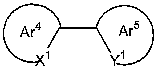
- the d-block metals form organometallic complexes with carbon or nitrogen donors such as porphyrin or bidentate ligands of formula (VI) :
- Ar 4 and Ar 5 may be the same or different and are independently selected from optionally substituted aryl or heteroaryl groups; X 1 and Y 1 may be the same or different and are independently selected from carbon or nitrogen; and Ar 4 and Ar 5 may be fused together.
- Ligands wherein X 1 is carbon and Y 1 is nitrogen are particularly preferred.
- Each of Ar 4 and Ar 5 may carry one or more substituents .
- substituents include fluorine or trifluoromethyl which may be used to blue-shift the emission of the complex as disclosed in WO 02/45466, WO 02/44189, US 2002-117662 and US 2002-182441; alkyl or alkoxy groups as disclosed in JP 2002-324679; carbazole which may be used to assist hole transport to the complex when used as an emissive material as disclosed in WO 02/81448; bromine, chlorine or iodine which can serve to functionalise the ligand for attachment of further groups as disclosed in WO 02/68435 and EP 1245659; and dendrons which may be used to obtain or enhance solution processability of the metal complex as disclosed in WO 02/66552.
- the phosphorescent metal complex may also be present in a polymeric or oligomeric chain as disclosed in WO 03/091355, in which case the complex may be present as a single unit or a repeat unit located within, pendant from, or as an end group of, a polymeric or oligomeric chain.
- ligands suitable for use with d-block elements include diketonates, in particular acetylacetonate (acac) ; triarylphosphines and pyridine, each of which may be substituted.
- the phosphorescent layer may be deposited during device manufacture by any suitable technique.
- the phosphorescent layer may be deposited by solution processing or vacuum evaporation.
- the thickness of the phosphorescent layer is in the range of from 5 to 200 nm. More preferably, the thickness of the phosphorescent layer is in the range of from 10 to 50 nm.
- the triplet energy level Ti of the phosphorescent layer preferably is no more than 0.1 eV greater than the T 1 level of the exciton generating material. More preferably, the Ti level of the phosphorescent material is no greater than the Ti level of the exciton generating material. Most preferably, the Ti level of the phosphorescent material is lower than the Ti level of the exciton generating material. According to a first embodiment, a singlet blocking layer is located between the exciton generating layer and the phosphorescent layer.
- the singlet blocking layer inhibits diffusion of singlet excitons, thereby retaining them in the exciton generating layer.
- the singlet blocking layer allows the diffusion of triplet excitons therethrough without quenching them.
- the singlet blocking layer has its Si (lowest energy level for singlet excitons) more than O.leV higher than the Si of the exciton generating layer. Also preferably, the singlet blocking layer has its Ti (lowest energy level for triplet excitons) not higher than that of the exciton generating layer. This is shown in Figure 2.
- a suitable material for the singlet blocking layer will be known to a person skilled in the art.
- a preferred material for the singlet blocking layer is stilbene.
- the singlet blocking layer must be sufficiently thin that triplet excitons are capable of diffusing through it.
- the thickness of the singlet blocking layer is in the range of from 10 to 70 nm. More preferably, the thickness of the singlet blocking layer is in the range of from 20 to 50 nm.
- the singlet blocking layer may be deposited during device manufacture by any suitable technique.
- the singlet blocking layer may be deposited by solution processing.
- the exciton generating layer is situated on the anode side of the device and the phosphorescent layer is situated on the cathode side of the device.
- the exciton generating layer must be sufficiently thin that triplet excitons are able to diffuse through it.
- the exciton generating layer is up to 50 nm thick.
- the device comprises a hole transporting layer with low electron mobility on which is formed an electron transporting, exciton generating layer with low hole mobility.
- This architecture is used to ensure that the recombination zone is close to the anode, with a sufficiently thick exciton generating layer so that singlet excitons can not diffuse as far as the phosphorescent layer due to their short half life.
- the thickness of the exciton generating layer is such that triplet excitons are able to diffuse to the phosphorescent layer because of their longer life.
- the thickness of the exciton generating layer is in the range of from 10 to 50 nm.
- the exciton generating layer should be sufficiently thick that singlet excitons do not diffuse out of it, but sufficiently thin that triplet excitons do diffuse out of it.
- exciton formation occurs in a recombination zone near or at the interface of the light emitting layer with the hole transport layer (HTL) (or the anode where a HTL is not present) .
- HTL hole transport layer
- the exciton generating layer is situated on the anode side of the device and the phosphorescent layer is situated on the cathode side of the device. In this case, the recombination zone will be in the exciton generating layer.
- the electrons In order for the holes and electrons to combine to generate excitons, the electrons thus must pass through the phosphorescent layer to reach the recombination zone in the exciton generating layer. Therefore, the phosphorescent layer must be capable of transporting electrons.
- the second embodiment is preferred.
- the anode may comprise any suitable material.
- An indium tin oxide (ITO) anode is preferred.
- a layer of conducting polymer is preferably provided over the anode.
- Poly(ethylene dioxythiophene) / poly(styrene sulfonate) is a preferred conducting polymer.
- the cathode may comprise any suitable material.
- the cathode may comprise a metal having a workfunction of below 3eV, such as calcium or barium, optionally with a higher workfunction capping material such as aluminium.
- the cathode may alternatively comprise a thin layer of electron injecting material such as a metal fluoride or oxide (e.g. LiF) and a metal layer (e.g. Al) .
- a metal fluoride or oxide e.g. LiF
- a metal layer e.g. Al
- solution processing this may be achieved, for example, by depositing a further layer from a solvent in which the underlying layer is not soluble. Alternatively, this may be achieved by rendering the underlying layer insoluble prior to deposition of the further layer thereon.
- the term "solution processable material/layer” encompasses both
- a preferred solution processing technique is spin-coating for forming unpatterned devices such as lighting devices.
- Ink jet printing is a preferred solution processing technique for forming a pixellated, high information content display.
- a further aspect of the present invention provides an illumination device (e.g. a flat illumination panel) comprising a light emitting device as defined above.
- an illumination device e.g. a flat illumination panel
- Such an illumination device may be used as a backlight for a liquid crystal display.
- a further aspect provides a method of making a light emitting device as defined above.
- the exciton generating layer and/or the phosphorescent layer is deposited by solution processing.
- the singlet blocking layer is deposited by solution processing the present method.
- the hole transport layer preferably is deposited by solution processing in the present method.
- Figure 1 shows the structure of a device according to the first embodiment of the invention
- Figure 2 shows energy of singlet (Si) and triplet (Ti) excitons relative to the ground state (So) in the exciton generating layer and the phosphorescent layer in a device according to the first embodiment of the invention.
- layer #1 is the singlet blocking layer and layer #2 is the exciton generating layer.
- Figure 3 shows the structure of a device according to the second embodiment of the invention
- a layer of PEDOT / PSS (available from H C Starck, Leverkusen, Germany as Baytron P ®) by spin-coating.
- Blue polymer Pl illustrated below and disclosed in WO 2003/095586, was deposited onto the F8-TFB layer to form a 25 nm thick exciton generating layer onto which was deposited by evaporation a mixture of Bt2lr (acac) :BCP in a weight ratio of 10:90 to form a 50 nm thick yellow emitting phosphorescent layer, and finally a cathode comprising a thin layer of LiF and a capping layer of aluminium was deposited over the BCP layer.
- the device was encapsulated by placing a metal enclosure over the device (available from Saes Getters SpA) and gluing it to the substrate to form an airtight seal.
Landscapes
- Physics & Mathematics (AREA)
- Optics & Photonics (AREA)
- Electroluminescent Light Sources (AREA)
Abstract
Description


Claims
Priority Applications (4)
| Application Number | Priority Date | Filing Date | Title |
|---|---|---|---|
| US11/664,543 US7944139B2 (en) | 2004-10-08 | 2005-10-07 | Light emitting device |
| JP2007535241A JP2008516440A (en) | 2004-10-08 | 2005-10-07 | Light emitting device |
| GB0705229A GB2433838B (en) | 2004-10-08 | 2005-10-07 | Light emitting device |
| DE112005002479T DE112005002479T5 (en) | 2004-10-08 | 2005-10-07 | Light emitting device |
Applications Claiming Priority (2)
| Application Number | Priority Date | Filing Date | Title |
|---|---|---|---|
| GBGB0422391.3A GB0422391D0 (en) | 2004-10-08 | 2004-10-08 | Light emitting device |
| GB0422391.3 | 2004-10-08 |
Publications (1)
| Publication Number | Publication Date |
|---|---|
| WO2006038020A1 true WO2006038020A1 (en) | 2006-04-13 |
Family
ID=33443605
Family Applications (1)
| Application Number | Title | Priority Date | Filing Date |
|---|---|---|---|
| PCT/GB2005/003864 WO2006038020A1 (en) | 2004-10-08 | 2005-10-07 | Light emitting device |
Country Status (6)
| Country | Link |
|---|---|
| US (1) | US7944139B2 (en) |
| JP (1) | JP2008516440A (en) |
| DE (1) | DE112005002479T5 (en) |
| GB (3) | GB0422391D0 (en) |
| TW (1) | TWI389364B (en) |
| WO (1) | WO2006038020A1 (en) |
Cited By (14)
| Publication number | Priority date | Publication date | Assignee | Title |
|---|---|---|---|---|
| WO2008123178A1 (en) | 2007-03-23 | 2008-10-16 | Idemitsu Kosan Co., Ltd. | Organic el device |
| WO2009008346A1 (en) * | 2007-07-07 | 2009-01-15 | Idemitsu Kosan Co., Ltd. | Organic el device |
| WO2009008357A1 (en) * | 2007-07-07 | 2009-01-15 | Idemitsu Kosan Co., Ltd. | Organic el device |
| WO2009008356A1 (en) * | 2007-07-07 | 2009-01-15 | Idemitsu Kosan Co., Ltd. | Organic el device |
| EP2023420A1 (en) * | 2007-08-07 | 2009-02-11 | OSRAM Opto Semiconductors GmbH | Ray-emitting device |
| DE102007053396A1 (en) * | 2007-08-07 | 2009-02-12 | Osram Opto Semiconductors Gmbh | Radiation-emitting device |
| DE102008039361A1 (en) * | 2008-05-30 | 2009-12-03 | Osram Opto Semiconductors Gmbh | Electronic device |
| WO2010016994A1 (en) * | 2008-08-07 | 2010-02-11 | General Electric Company | Method of manufacture of a multi-layer phosphorescent organic light emitting device, and articles thereof |
| DE102008054234A1 (en) * | 2008-10-31 | 2010-05-06 | Osram Opto Semiconductors Gmbh | Radiation-emitting device |
| US8294142B2 (en) | 2007-07-07 | 2012-10-23 | Idemitsu Kosan Co., Ltd. | Organic EL device |
| JP2015015261A (en) * | 2006-10-27 | 2015-01-22 | ユニバーシティ オブ サザン カリフォルニア | Substances and structures for efficiently harvesting singlet and triplet excitons for white oled |
| US9082995B2 (en) | 2007-07-07 | 2015-07-14 | Idemitsu Kosan Co., Ltd. | Organic EL element and organic EL material-containing solution |
| US10014487B2 (en) | 2013-09-17 | 2018-07-03 | Kyulux, Inc. | Organic electroluminescent device |
| US10439158B2 (en) | 2013-12-02 | 2019-10-08 | Semiconductor Energy Laboratory Co., Ltd. | Light-emitting element, light-emitting device, electronic appliance, and lighting device |
Families Citing this family (15)
| Publication number | Priority date | Publication date | Assignee | Title |
|---|---|---|---|---|
| JP4967952B2 (en) * | 2007-09-21 | 2012-07-04 | セイコーエプソン株式会社 | LIGHT EMITTING ELEMENT, DISPLAY DEVICE, AND ELECTRONIC DEVICE |
| KR101453874B1 (en) * | 2008-03-04 | 2014-10-21 | 삼성디스플레이 주식회사 | White organic light emitting device |
| JP5465088B2 (en) * | 2010-05-31 | 2014-04-09 | キヤノン株式会社 | Organic electroluminescence device |
| WO2012111579A1 (en) | 2011-02-16 | 2012-08-23 | Semiconductor Energy Laboratory Co., Ltd. | Light-emitting element |
| US8502445B2 (en) * | 2011-07-18 | 2013-08-06 | Universal Display Corporation | RGBW OLED display for extended lifetime and reduced power consumption |
| WO2013039914A1 (en) | 2011-09-12 | 2013-03-21 | Nitto Denko Corporation | Efficient organic light-emitting diodes and fabrication of the same |
| JP5487174B2 (en) * | 2011-09-16 | 2014-05-07 | 株式会社東芝 | Organic electroluminescent element, display device and lighting device |
| GB201200823D0 (en) * | 2012-01-18 | 2012-02-29 | Cambridge Display Tech Ltd | Electroluminescence |
| US9917281B2 (en) | 2012-09-07 | 2018-03-13 | Nitto Denko Corporation | Top-emitting white organic light-emitting diodes having improved efficiency and stability |
| US9859517B2 (en) | 2012-09-07 | 2018-01-02 | Nitto Denko Corporation | White organic light-emitting diode |
| US8786179B2 (en) * | 2012-09-17 | 2014-07-22 | Universal Display Corporation | Light emitting device comprising phosphorescent materials for white light generation |
| US20160163987A1 (en) * | 2013-07-29 | 2016-06-09 | Merck Patent Gmbh | Electro-optical device and the use thereof |
| CN104347808B (en) * | 2014-09-16 | 2017-06-23 | 太原理工大学 | A kind of color stability white light organic electroluminescent device high |
| TWI611612B (en) | 2016-11-30 | 2018-01-11 | 財團法人工業技術研究院 | Organic light-emitting diode and white organic light-emitting diode |
| CN111799386B (en) * | 2020-07-22 | 2023-07-14 | 京东方科技集团股份有限公司 | Light-emitting device and display device |
Citations (1)
| Publication number | Priority date | Publication date | Assignee | Title |
|---|---|---|---|---|
| US20020182441A1 (en) * | 2000-08-11 | 2002-12-05 | Trustee Of Princeton University | Organometallic compounds and emission-shifting organic electrophosphorescence |
Family Cites Families (26)
| Publication number | Priority date | Publication date | Assignee | Title |
|---|---|---|---|---|
| US6309763B1 (en) | 1997-05-21 | 2001-10-30 | The Dow Chemical Company | Fluorene-containing polymers and electroluminescent devices therefrom |
| DE69824439T2 (en) | 1997-10-23 | 2005-06-16 | Isis Innovation Ltd., Summertown | LIGHT-EMITTING DENDRIMERS |
| DE69941200D1 (en) * | 1998-01-09 | 2009-09-17 | Sony Corp | Electroluminescent device and manufacturing method |
| KR100798562B1 (en) | 2000-11-30 | 2008-01-31 | 캐논 가부시끼가이샤 | Luminescent Element and Display |
| KR100533556B1 (en) | 2000-11-30 | 2005-12-06 | 캐논 가부시끼가이샤 | Luminescent element and display |
| US6693295B2 (en) | 2000-12-25 | 2004-02-17 | Fuji Photo Film Co., Ltd. | Indole derivative, material for light-emitting device and light-emitting device using the same |
| GB0104177D0 (en) | 2001-02-20 | 2001-04-11 | Isis Innovation | Aryl-aryl dendrimers |
| DE60239730D1 (en) | 2001-02-20 | 2011-05-26 | Isis Innovation | METAL CONTAINING DENDRIMERE |
| DE10109027A1 (en) | 2001-02-24 | 2002-09-05 | Covion Organic Semiconductors | Rhodium and iridium complexes |
| SG92833A1 (en) | 2001-03-27 | 2002-11-19 | Sumitomo Chemical Co | Polymeric light emitting substance and polymer light emitting device using the same |
| SK12082003A3 (en) | 2001-04-05 | 2004-09-08 | Sankyo Company Limited | Benzamidine derivatives |
| JP2002324679A (en) | 2001-04-26 | 2002-11-08 | Honda Motor Co Ltd | Organic electroluminescent element |
| GB0111549D0 (en) * | 2001-05-11 | 2001-07-04 | Cambridge Display Tech Ltd | Polymers, their preparation and uses |
| AU2002305548A1 (en) * | 2001-05-16 | 2002-11-25 | The Trustees Of Princeton University | High efficiency multi-color electro-phosphorescent oleds |
| US7034339B2 (en) * | 2001-08-09 | 2006-04-25 | Idemitsu Kosan Co., Ltd. | Organic EL display device having host compound and phosphorescent luminous compound, and method of driving same |
| GB0209652D0 (en) * | 2002-04-26 | 2002-06-05 | Univ Cambridge Tech | Solution-processable phosphorescent materials |
| JP5069401B2 (en) | 2002-05-10 | 2012-11-07 | ケンブリッジ ディスプレイ テクノロジー リミテッド | Polymer and production method thereof |
| ATE468618T1 (en) | 2002-09-03 | 2010-06-15 | Cambridge Display Tech Ltd | METHOD FOR PRODUCING AN OPTICAL DEVICE |
| JP2004200141A (en) * | 2002-10-24 | 2004-07-15 | Toyota Industries Corp | Organic el element |
| US7063900B2 (en) * | 2002-12-23 | 2006-06-20 | General Electric Company | White light-emitting organic electroluminescent devices |
| JP4519652B2 (en) * | 2002-12-26 | 2010-08-04 | 株式会社半導体エネルギー研究所 | Organic light emitting device |
| JP2004217592A (en) * | 2003-01-16 | 2004-08-05 | Mitsubishi Chemicals Corp | Iminostilbene-based compound, charge transport material, organic electroluminescent device material, and organic electroluminescent device |
| JP4096877B2 (en) * | 2003-02-07 | 2008-06-04 | 松下電器産業株式会社 | Information reading element and information reading device using the same |
| DE10310887A1 (en) * | 2003-03-11 | 2004-09-30 | Covion Organic Semiconductors Gmbh | Matallkomplexe |
| US7029766B2 (en) * | 2003-12-05 | 2006-04-18 | Eastman Kodak Company | Organic element for electroluminescent devices |
| TWI471058B (en) * | 2005-06-01 | 2015-01-21 | Univ Princeton | Fluorescent filtered electrophosphorescence |
-
2004
- 2004-10-08 GB GBGB0422391.3A patent/GB0422391D0/en not_active Ceased
-
2005
- 2005-10-07 GB GB0903915A patent/GB2455924A/en not_active Withdrawn
- 2005-10-07 WO PCT/GB2005/003864 patent/WO2006038020A1/en active Application Filing
- 2005-10-07 DE DE112005002479T patent/DE112005002479T5/en not_active Ceased
- 2005-10-07 US US11/664,543 patent/US7944139B2/en not_active Expired - Fee Related
- 2005-10-07 JP JP2007535241A patent/JP2008516440A/en active Pending
- 2005-10-07 GB GB0705229A patent/GB2433838B/en not_active Expired - Fee Related
- 2005-10-07 TW TW094135291A patent/TWI389364B/en not_active IP Right Cessation
Patent Citations (1)
| Publication number | Priority date | Publication date | Assignee | Title |
|---|---|---|---|---|
| US20020182441A1 (en) * | 2000-08-11 | 2002-12-05 | Trustee Of Princeton University | Organometallic compounds and emission-shifting organic electrophosphorescence |
Non-Patent Citations (3)
| Title |
|---|
| DESHPANDE R S ET AL: "WHITE-LIGHT-EMITTING ORGANIC ELECTROLUMINESCENT DEVICES BASED ON INTERLAYER SEQUENTIAL ENERGY TRANSFER", APPLIED PHYSICS LETTERS, AIP, AMERICAN INSTITUTE OF PHYSICS, MELVILLE, NY, US, vol. 75, no. 7, 16 August 1999 (1999-08-16), pages 888 - 890, XP000875531, ISSN: 0003-6951 * |
| TOKITO SHIZUO ET AL: "High-efficiency white phosphorescent organic light-emitting devices with greenish-blue and red-emitting layers", APPLIED PHYSICS LETTERS, AIP, AMERICAN INSTITUTE OF PHYSICS, MELVILLE, NY, US, vol. 83, no. 12, 22 September 2003 (2003-09-22), pages 2459 - 2461, XP012035185, ISSN: 0003-6951 * |
| TSUJI TOSHIE ET AL: "Nondoped-type white organic electroluminescent devices utilizing complementary color and exciton diffusion", APPLIED PHYSICS LETTERS, AIP, AMERICAN INSTITUTE OF PHYSICS, MELVILLE, NY, US, vol. 81, no. 18, 28 October 2002 (2002-10-28), pages 3329 - 3331, XP012032304, ISSN: 0003-6951 * |
Cited By (24)
| Publication number | Priority date | Publication date | Assignee | Title |
|---|---|---|---|---|
| JP2015015261A (en) * | 2006-10-27 | 2015-01-22 | ユニバーシティ オブ サザン カリフォルニア | Substances and structures for efficiently harvesting singlet and triplet excitons for white oled |
| WO2008123178A1 (en) | 2007-03-23 | 2008-10-16 | Idemitsu Kosan Co., Ltd. | Organic el device |
| US8207526B2 (en) | 2007-03-23 | 2012-06-26 | Idemitsu Kosan Co., Ltd. | Organic EL device |
| JPWO2008123178A1 (en) * | 2007-03-23 | 2010-07-15 | 出光興産株式会社 | Organic EL device |
| WO2009008346A1 (en) * | 2007-07-07 | 2009-01-15 | Idemitsu Kosan Co., Ltd. | Organic el device |
| WO2009008357A1 (en) * | 2007-07-07 | 2009-01-15 | Idemitsu Kosan Co., Ltd. | Organic el device |
| WO2009008356A1 (en) * | 2007-07-07 | 2009-01-15 | Idemitsu Kosan Co., Ltd. | Organic el device |
| US9082995B2 (en) | 2007-07-07 | 2015-07-14 | Idemitsu Kosan Co., Ltd. | Organic EL element and organic EL material-containing solution |
| US8436343B2 (en) | 2007-07-07 | 2013-05-07 | Idemitsu Kosan Co., Ltd. | Organic EL device |
| US8426036B2 (en) | 2007-07-07 | 2013-04-23 | Idemitsu Kosan Co., Ltd. | Organic EL device and anthracene derivative |
| US8294142B2 (en) | 2007-07-07 | 2012-10-23 | Idemitsu Kosan Co., Ltd. | Organic EL device |
| JPWO2009008356A1 (en) * | 2007-07-07 | 2010-09-09 | 出光興産株式会社 | Organic EL device |
| US8173998B2 (en) | 2007-08-07 | 2012-05-08 | Osram Opto Semiconductors Gmbh | Radiation emitting device |
| JP2009044130A (en) * | 2007-08-07 | 2009-02-26 | Osram Opto Semiconductors Gmbh | Radiation emitting device |
| US8610114B2 (en) | 2007-08-07 | 2013-12-17 | Osram Opto Semiconductors Gmbh | Radiation emitting device |
| DE102007053396A1 (en) * | 2007-08-07 | 2009-02-12 | Osram Opto Semiconductors Gmbh | Radiation-emitting device |
| EP2023420A1 (en) * | 2007-08-07 | 2009-02-11 | OSRAM Opto Semiconductors GmbH | Ray-emitting device |
| DE102008039361A1 (en) * | 2008-05-30 | 2009-12-03 | Osram Opto Semiconductors Gmbh | Electronic device |
| US8723164B2 (en) | 2008-05-30 | 2014-05-13 | Osram Opto Semiconductors Gmbh | Electronic device |
| WO2010016994A1 (en) * | 2008-08-07 | 2010-02-11 | General Electric Company | Method of manufacture of a multi-layer phosphorescent organic light emitting device, and articles thereof |
| DE102008054234A1 (en) * | 2008-10-31 | 2010-05-06 | Osram Opto Semiconductors Gmbh | Radiation-emitting device |
| US8816329B2 (en) | 2008-10-31 | 2014-08-26 | Osram Opto Semiconductors Gmbh | Radiation-emitting device |
| US10014487B2 (en) | 2013-09-17 | 2018-07-03 | Kyulux, Inc. | Organic electroluminescent device |
| US10439158B2 (en) | 2013-12-02 | 2019-10-08 | Semiconductor Energy Laboratory Co., Ltd. | Light-emitting element, light-emitting device, electronic appliance, and lighting device |
Also Published As
| Publication number | Publication date |
|---|---|
| GB0903915D0 (en) | 2009-04-22 |
| GB2455924A (en) | 2009-07-01 |
| TWI389364B (en) | 2013-03-11 |
| TW200625708A (en) | 2006-07-16 |
| GB2433838A (en) | 2007-07-04 |
| GB0705229D0 (en) | 2007-04-25 |
| DE112005002479T5 (en) | 2007-11-08 |
| US7944139B2 (en) | 2011-05-17 |
| US20080258606A1 (en) | 2008-10-23 |
| GB2433838B (en) | 2009-11-25 |
| JP2008516440A (en) | 2008-05-15 |
| GB0422391D0 (en) | 2004-11-10 |
Similar Documents
| Publication | Publication Date | Title |
|---|---|---|
| US7944139B2 (en) | Light emitting device | |
| KR100934420B1 (en) | Very high efficiency organic light emitting devices based on electrophosphorescence | |
| EP2887417B1 (en) | Extended OLED operational lifetime through phosphorescent dopant profile mangement | |
| TWI547542B (en) | White light emitting material | |
| US20030175553A1 (en) | White light emitting oleds from combined monomer and aggregate emission | |
| JP4966203B2 (en) | Light emitting device | |
| KR20130129949A (en) | Polymer and organic light-emitting device | |
| JP2003526876A5 (en) | ||
| US20100096978A1 (en) | Light Emissive Device | |
| Suzuki et al. | High-efficiency white phosphorescent polymer light-emitting devices | |
| JP2009525605A5 (en) | ||
| WO2007071969A2 (en) | Light emissive device | |
| Suzuki et al. | White light emission from polymer light-emitting devices based on blue and red phosphorescent polymers | |
| KR100928236B1 (en) | White light-emitting organic light emitting device in which radiation from monomers and aggregates is mixed | |
| KR100757780B1 (en) | Polymer-based electrophosphorescent devices by controlled morphology of emitting layer |
Legal Events
| Date | Code | Title | Description |
|---|---|---|---|
| AK | Designated states |
Kind code of ref document: A1 Designated state(s): AE AG AL AM AT AU AZ BA BB BG BR BW BY BZ CA CH CN CO CR CU CZ DE DK DM DZ EC EE EG ES FI GB GD GE GH GM HR HU ID IL IN IS JP KE KG KM KP KR KZ LC LK LR LS LT LU LV LY MA MD MG MK MN MW MX MZ NA NG NI NO NZ OM PG PH PL PT RO RU SC SD SE SG SK SL SM SY TJ TM TN TR TT TZ UA UG US UZ VC VN YU ZA ZM ZW |
|
| AL | Designated countries for regional patents |
Kind code of ref document: A1 Designated state(s): GM KE LS MW MZ NA SD SL SZ TZ UG ZM ZW AM AZ BY KG KZ MD RU TJ TM AT BE BG CH CY CZ DE DK EE ES FI FR GB GR HU IE IS IT LT LU LV MC NL PL PT RO SE SI SK TR BF BJ CF CG CI CM GA GN GQ GW ML MR NE SN TD TG |
|
| 121 | Ep: the epo has been informed by wipo that ep was designated in this application | ||
| ENP | Entry into the national phase |
Ref document number: 0705229 Country of ref document: GB Kind code of ref document: A Free format text: PCT FILING DATE = 20051007 |
|
| WWE | Wipo information: entry into national phase |
Ref document number: 0705229.3 Country of ref document: GB |
|
| WWE | Wipo information: entry into national phase |
Ref document number: 2007535241 Country of ref document: JP |
|
| WWE | Wipo information: entry into national phase |
Ref document number: 1120050024792 Country of ref document: DE |
|
| RET | De translation (de og part 6b) |
Ref document number: 112005002479 Country of ref document: DE Date of ref document: 20071108 Kind code of ref document: P |
|
| 122 | Ep: pct application non-entry in european phase |
Ref document number: 05796347 Country of ref document: EP Kind code of ref document: A1 |
|
| WWE | Wipo information: entry into national phase |
Ref document number: 11664543 Country of ref document: US |