明細: 有機電界発光素子、 及びそれを用いた発光装置又は表示装置 技術分野 Description: Organic electroluminescent element, and light emitting device or display device using the same
本発明は、 発光領域を有する有機層が陽極と陰極との間に設けられて いる有機電界発光素子 (有機 E L素子) 、 及びこれを用いたディスプレ イデバイス等の発光又は表示装置に関するものである。 背景技術 The present invention relates to an organic electroluminescent element (organic EL element) in which an organic layer having a light emitting region is provided between an anode and a cathode, and a light emitting or display device using the same, such as a display device. . Background art
軽量で高効率のフラットパネルディスプレイが、 例えばコンピュータ やテレビジョンの画面表示用として盛んに研究、 開発されている。 まず、 ブラウン管 (C R T ) は、 輝度が高く、 色再現性が良いため、 現在ディスプレイとして最も多く使われているが、 嵩高く、 重く、 また 消費電力も高いという問題がある。 Lightweight and highly efficient flat panel displays are being actively researched and developed, for example, for use in computer and television screen displays. First, cathode ray tubes (CRTs) are currently used most often as displays because of their high brightness and good color reproduction, but they have the problem of being bulky, heavy, and high in power consumption.
また、 軽量で高効率のフラットパネルディスプレイとして、 ァクティ ブマトリックス駆動等の液晶ディスプレイが商品化されているが、 液晶 ディスプレイは視野角が狭く、 また自発光でないために、 周囲が暗い環 境下ではバックライ 卜の消費電力が大きいことや、 今後実用化が期待さ れている高精細度の高速ビデオ信号に対して十分な応答性能を有しない 等の問題点がある。 特に、 大画面サイズのディスプレイを製造すること は困難であり、 そのコストが高いこと等の課題もある。 Liquid crystal displays such as active matrix drive have been commercialized as lightweight, high-efficiency flat panel displays.However, liquid crystal displays have a narrow viewing angle and do not emit light. There are problems such as the large power consumption of the backlight and the lack of sufficient response performance to high-definition high-speed video signals expected to be put to practical use in the future. In particular, it is difficult to manufacture a large screen display, and there are also problems such as high cost.
これに対する代替として、 発光ダイォ一ドを用いたディスプレイの可 能性があるが、 やはり製造コストが高く、 また、 1つの基板上に発光ダ ィオードのマトリックス構造を形成することが難しい等の問題があり、 ブラウン管に取って代わる低価格のディスプレイ候補としては、 実用化
までの課題が大きい。 As an alternative to this, there is a possibility of a display using a light-emitting diode, but it still has high manufacturing costs and it is difficult to form a matrix structure of light-emitting diodes on one substrate. Available as a low-cost display candidate to replace CRT The challenge is big.
これらの諸課題を解決する可能性のあるフラッ卜パネルディスプレイ として、 最近、 有機発光材料を用いた有機電界発光素子 (有機 EL素 子) が注目されている。 即ち、 発光材料として有機化合物を用いること により、 自発光で、 応答速度が高速であり、 視野角依存性の無いフラッ トパネルディスプレイの実現が期待されている。 Recently, an organic electroluminescent element (organic EL element) using an organic light emitting material has been attracting attention as a flat panel display that can solve these problems. That is, by using an organic compound as a light emitting material, realization of a flat panel display which is self-luminous, has a high response speed, and has no viewing angle dependence is expected.
有機電界発光素子の構成は、 透光性の正極と金属陰極との間に、 電流 の注入によって発光する発光材料を含む有機薄膜を形成したものである C. W. Tang, S. A. VanSlyke等は Applied Physics Letters第 5 1卷 1 2号 9 1 3〜 9 1 5頁 ( 1 9 8 7年) 掲載の研究報告において、 有機薄 膜を正孔輸送性材料からなる薄膜と電子輸送性材料からなる薄膜との 2 層構造として、 各々の電極から有機薄膜中に注入された正孔 (ホール) と電子が再結合することにより発光する素子構造を開発した (シンダル ヘテロ構造の有機 EL素子) 。 The structure of an organic electroluminescent device is a device in which an organic thin film containing a light emitting material that emits light by current injection is formed between a translucent positive electrode and a metal cathode. CW Tang, SA VanSlyke et al., Applied Physics Letters 5 1 Vol. 12 No. 9 9 3 9 pp. 15 (19987) In a research report published in 1987, two types of organic thin films were used: thin films composed of hole transport materials and thin films composed of electron transport materials. As the layer structure, we have developed a device structure that emits light by recombination of electrons and holes injected from each electrode into the organic thin film (organic EL device with sindal hetero structure).
この素子構造では、 正孔輸送材料または電子輸送材料のいずれかが発 光材料を兼ねており、 発光は発光材料の基底状態と励起状態のエネルギ 一ギャップに対応した波長帯で起きる。 このような 2層構造とすること により、 大幅な駆動電圧の低減、 発光効率の改善が行われた。 In this device structure, either the hole transporting material or the electron transporting material also functions as the light emitting material, and light emission occurs in a wavelength band corresponding to the energy gap between the ground state and the excited state of the light emitting material. By adopting such a two-layer structure, drastic reduction in driving voltage and improvement in luminous efficiency were achieved.
その後、 Adachi 、 S. Tokita、 T. TsutsuK S. Saito等の Then, Adachi, S. Tokita, T. TsutsuK S. Saito, etc.
Japanese Journal of Applied Physics第 2 7巻 2号 L 2 6 9〜L 2 7 1頁 (1 9 8 8年) 掲載の研究報告に記載されているように、 正孔輸送 材料、 発光材料、 電子輸送材料の 3層構造 (ダブルへテロ構造の有機 E L素子) が開発され、 更に、 W. Tang, S. A. VanSlyke, C. H. Chen 等の Journal of Applied Physics 第 6 5巻 9号 3 6 1 0〜3 6 1 6頁 ( 1 9 8 9年) 掲載の研究報告に記載されているように、 電子輸送材料 中に発光材料を含ませた素子構造などが開発された。 これらの研究によ
り、 低電圧で、 高輝度の発光の可能性が検証され、 近年、 研究開発が非 常に活発に行われている。 Japanese Journal of Applied Physics Vol. 27 No. 2 L269-L27 1 (1989) As described in the research report published in this report, hole transport materials, luminescent materials, and electron transport A three-layer structure (organic EL device with a double hetero structure) of materials was developed, and furthermore, Journal of Applied Physics, Vol. 65 No. 9 No. 3 61 0-36 1 by W. Tang, SA VanSlyke, CH Chen et al. As described in the research report on page 6 (1989), a device structure in which a luminescent material was included in an electron transport material was developed. Based on these studies The possibility of high-brightness light emission at low voltage has been verified, and research and development has been very active in recent years.
発光材料に用いる有機化合物は、 その多様性から、 理論的には分子構 造を変化させることによって発光色を任意に変えることができるという 利点があると言える。 従って、 分子設計を施すことにより、 フルカラー ディスプレイに必要な色純度の良い R (赤) 、 G (緑) 、 B (青) の 3 色を揃えることは、 無機物を用いた薄膜 EL素子と比べて容易であると 言える。 The diversity of organic compounds used in light-emitting materials has the advantage that the emission color can be changed arbitrarily by changing the molecular structure theoretically. Therefore, by applying molecular design, the three colors of R (red), G (green), and B (blue) with good color purity required for a full-color display can be compared with thin-film EL devices using inorganic substances. It can be said that it is easy.
現在、 後記の非特許文献 1で報告されているように、 電子輸送材料と して、 トリス (8—キノリール) アルミニウム (以下、 A 1 q3と略記 する。 ) に 4—ジシァノメチレン一 6— (p—ジメチルアミノスチリ ル) — 2—メチル— 4H—ピラン (以下、 DCMと略記する。 ) をド一 プした赤色発光の例等がある。 Currently, as reported in below the non-patent document 1, as an electron transport material, tris (8-Kinoriru) aluminum (hereinafter abbreviated as A 1 q 3.) 4-Jishianomechiren one 6- ( There is an example of red light emission obtained by doping p-dimethylaminostyrene) -2-methyl-4H-pyran (hereinafter abbreviated as DCM).
また、 後記の非特許文献 2で報告されている B S B— B CNは、 1 0 0 0 c dZm2以上の高い輝度を実現している。 Also been reported in below the non-patent document 2 BSB- B CN realizes a 1 0 0 0 c dZm 2 or more high brightness.
また、 後記の特許文献 1においては、 特定のスチリル化合物を有機電 界発光材料とすることを提案している。 Patent Document 1 described below proposes that a specific styryl compound be used as an organic electroluminescent material.
非特許文献 1 : Chem.Funct.Dyes,Proc. Int. Sy即 ·, 2nd P.536 (1993) 非特許文南犬 2 : T. Tsutsui, D. U. Kim, Inorganic and Organic electroluminescence 会議 (1996、 Ber 1 in) Non-Patent Document 1: Chem. Func. Dyes, Proc. Int. Sy Immediately, 2nd P. 536 (1993) Non-patent document South Dog 2: T. Tsutsui, DU Kim, Inorganic and Organic electroluminescence conference (1996, Ber 1 in)
特許文献 1 :特開平 7— 1 88 649号 (特許請求の範囲、 第 5頁右 欄 8行目〜第 22頁右欄 5行目、 第 1図〜第 3図) Patent Document 1: Japanese Patent Application Laid-Open No. 7-188649 (claims, page 5, right column, line 8 to page 22, right column, line 5, FIG. 1 to FIG. 3)
しかしながら、 実際には有機電界発光素子においても、 解決しなけれ ばならない問題がある。 安定した高輝度の赤色発光素子の開発は難しく 上記非特許文献 1に示されている電子輸送材料のように A 1 q3に DC Mをドープした赤色発光の例等は、 輝度、 信頼性ともにディスプレイ材
料としては満足のいくものではない。 However, there are actually problems that need to be solved even in organic electroluminescent devices. Examples of red light-emitting doped with DC M to A 1 q 3 such as a stable high brightness electron transporting material development of the red light emitting element is shown in difficult Non-Patent Document 1 of the luminance, reliability both Display materials The fees are not satisfactory.
また、 上記非特許文献 2に示されている B S B— B C Nは、 1 0 0 0 c d Zm2以上の高い輝度を実現しているが、 フルカラーに対応する赤 色としての色度が完全なものとは言えない。 Also shown in Non-Patent Document 2 BSB- BCN is realizes a 1 0 0 0 cd Zm 2 or more high brightness, and chromaticity as red corresponding to full-color ones complete I can't say.
さらに高輝度で安定かつ色純度の高い赤色発光素子の実現が、 望まれ ているのが現状である。 At present, the realization of a red light-emitting element having high luminance, stability and high color purity is desired.
また、 上記特許文献 1においては、 特定のスチリル化合物を有機電界 発光材料とすることを提案しているが、 目的の発光色が青色であり、 赤 色等の他の色波長を得ることを目的としたものではない。 Also, Patent Document 1 proposes that a specific styryl compound be used as an organic electroluminescent material. However, the objective emission color is blue, and it is intended to obtain another color wavelength such as red. It is not something.
本発明の目的は、 高い蛍光収率を有し、 熱安定性にも優れた化合物を 用いて、 赤色等の比較的長波長の発光色を任意に選択でき、 色純度が良 く、 高輝度かつ安定な発光を生じる有機電界発光素子、 及びこれを用い た発光又は表示装置を提供することにある。 発明の開示 It is an object of the present invention to use a compound having a high fluorescence yield and excellent thermal stability to arbitrarily select an emission color of a relatively long wavelength such as red, and to have high color purity and high brightness. Another object of the present invention is to provide an organic electroluminescent element that generates stable light emission, and a light emitting or display device using the same. Disclosure of the invention
本発明者は、 上記課題を解決するために鋭意検討した結果、 特に、 特 定のスチリル化合物と、 これに効率良くエネルギーを伝達することが可 能な材料とから発光領域を構成した有機電界発光素子を作製すれば、 高 輝度、 高信頼性であって熱安定性も良好であり、 赤色等の比較的長波長 の色純度が良好な発光素子を提供できることを見出し、 本発明に到達し たものである。 図面の簡単な説明 The inventors of the present invention have conducted intensive studies to solve the above-mentioned problems, and as a result, in particular, an organic electroluminescent device having a light-emitting region composed of a specific styryl compound and a material capable of efficiently transmitting energy thereto. The present inventors have found that if a device is manufactured, a light-emitting device having high luminance, high reliability, good thermal stability, and excellent color purity at a relatively long wavelength such as red can be provided, and the present invention has been achieved. Things. BRIEF DESCRIPTION OF THE FIGURES
第 1図は、 本発明に基づく有機電界発光素子の要部概略断面図である。 第 2図は、 同、 有機電界発光素子の他の例の要部概略断面図である。 第 3図は、 同、 有機電界発光素子の他の例の要部概略断面図である。
第 4図は、 同、 有機電界発光素子の他の例の要部概略断面図である。 第 5図は、 同、 有機電界発光素子の他の例の要部概略断面図である。 第 6図は、 同、 有機電界発光素子の更に他の例の要部概略断面図であ る。 FIG. 1 is a schematic sectional view of a main part of an organic electroluminescent device according to the present invention. FIG. 2 is a schematic cross-sectional view of a main part of another example of the organic electroluminescent device. FIG. 3 is a schematic sectional view of a main part of another example of the organic electroluminescent device. FIG. 4 is a schematic cross-sectional view of a main part of another example of the organic electroluminescent device. FIG. 5 is a schematic sectional view of a main part of another example of the organic electroluminescent device. FIG. 6 is a schematic cross-sectional view of a main part of still another example of the organic electroluminescent device.
第 7図は、 同、 有機電界発光素子を用いたフルカラーの平面ディスプ レイの構成図である。 発明を実施するための最良の形態 FIG. 7 is a configuration diagram of a full-color flat display using the same organic electroluminescent device. BEST MODE FOR CARRYING OUT THE INVENTION
本発明は、 発光領域を有する有機層が陽極と陰極との間に設けられ、 電流の注入によって発光する有機物質を構成要素として含む有機電界発 光素子において、 前記有機層の構成層のうちの少 くとも 1層が、 下記 一般式 [ I ] で表されるスチリル化合物の少なくとも 1種 ( 1種であつ てよいが、 2種又はそれ以上であってもよレ^ ) と、 電荷輸送能を持つ 材料とを含む混合層からなることを特徴とする有機電界発光素子 (以下、 本発明の第 1の有機 EL素子と称すること力 Sある。 ) に係るものである 一般式 [ I ] : The present invention provides an organic electroluminescent device including an organic layer having a light-emitting region provided between an anode and a cathode, and including, as a component, an organic substance that emits light by current injection. At least one layer comprises at least one styryl compound represented by the following general formula [I] (there may be at least one styryl compound, or at least two styryl compounds); An organic electroluminescent device (hereinafter referred to as a first organic EL device of the present invention having a power S) comprising a mixed layer containing a material having the following general formula [I]:
Y— CH= CH— X Y— CH = CH— X
〔伹し、 前記一般式 [ I ] において、 Xは下記一般式 ( 1) 〜 (1 3) のいずれかで表される基であり [In the general formula [I], X is a group represented by any of the following general formulas (1) to (13).
(4) (5) (6) (4) (5) (6)
(7) (8) (9) (7) (8) (9)
(10) (Ten)
(11) (12) (13) (11) (12) (13)
(但し、 前記一般式 ( 1) において、 R1〜R5は少なくとも一つがハロ ゲン原子、 ニトロ基、 シァノ基、 トリフルォロメチル基、 置換基を有し てもよいアルキル基、 及び置換基を有してもよいアルコキシル基から選
ばれた基であり、 それらは同一であっても異なってもよい。 また、 前記 一般式 (2) 〜 ( 1 3) において、 R6〜R1119は、 水素原子、 フッ素原 子、 塩素原子等 (以下、 同様) のハロゲン原子、 ニトロ基、 シァノ基、 トリフルォロメチル基、 置換基を有してもよいアルキル基及び、 置換基 を有してもよいァリ一ル基、 及び置換基を有してもよいアルコキシル基 から選ばれた基であり、 それらは同一であっても異なってもよい。 ) 、 また、 前記一般式 [ I ] において、 Yは下記一般式 (14) 〜 ( 1 6) のいずれかで表される基である。 (However, in the general formula (1), at least one of R 1 to R 5 is a halogen atom, a nitro group, a cyano group, a trifluoromethyl group, an alkyl group which may have a substituent, and a substituent. Selected from alkoxyl groups which may have Groups, which may be the same or different. In the general formulas (2) to (13), R 6 to R 1119 represent a halogen atom such as a hydrogen atom, a fluorine atom, a chlorine atom or the like (the same applies hereinafter), a nitro group, a cyano group, and a trifluoro group. A methyl group, an alkyl group which may have a substituent, an aryl group which may have a substituent, and an alkoxyl group which may have a substituent. They may be the same or different. In the general formula [I], Y is a group represented by any of the following general formulas (14) to (16).
(15) (但し、 前記一般式 ( 14) において、 Z1および Z2は、 水素原子、 置 換基を有してもよいアルキル基、 及び置換基を有してもよいァリール基 から選ばれた基であり、 それらは同一であっても異なってもよい。 また、 前記一般式 ( 1 5) 及び (1 6) において、 R11 ()〜R126は、 水素原子、 置換基を有してもよいアルキル基、 置換基を有してもよいァリール基、 置換基を有してもよいアルコキシル基、 ハロゲン原子、 ニトロ基、 シァ ノ基及びトリフルォロメチル基から選ばれた基であり、 それらは同一で あっても異なってもよい。 ) ] (15) (However, in the general formula (14), Z 1 and Z 2 are each selected from a hydrogen atom, an alkyl group optionally having a substituent, and an aryl group optionally having a substituent. In the general formulas (15) and (16), R 11 () to R 126 each represent a hydrogen atom or a substituent. An alkyl group which may be substituted, an aryl group which may have a substituent, an alkoxyl group which may have a substituent, a halogen atom, a nitro group, a cyano group and a trifluoromethyl group. , They may be the same or different.
ここで、 前記一般式 [ I ] において、 R'〜R5はハロゲン原子、 ニト 口基等の置換基であることが不可欠であるが、 これは尺1〜 R5が水素原 子のときは赤色発光が得られない上に結晶性を低下させることができな
いからである。 Here, in the general formula [I], although R'~R 5 it is essential that a substituent such as a halogen atom, a nitro port group, which when scale 1 ~ R 5 is hydrogen atom is Red light emission cannot be obtained and crystallinity cannot be reduced. Because it is.
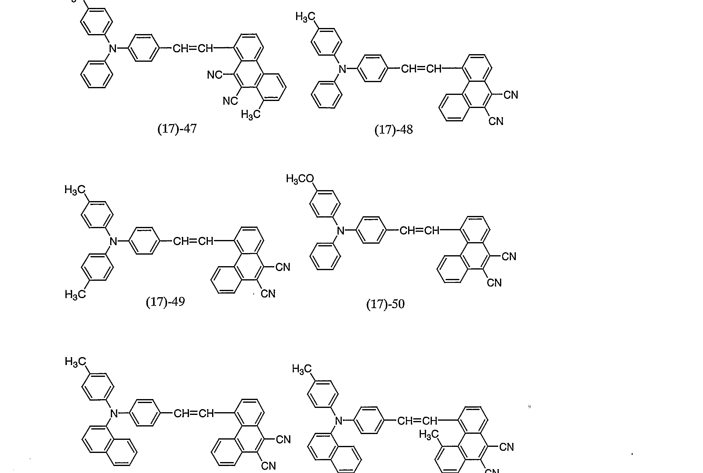
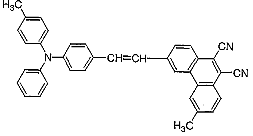
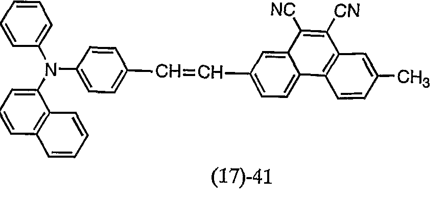
本発明の有機電界発光素子において、 前記一般式 [ I ] で示されるス チリル化合物としては、 下記構造式 (1 7) — 1〜 ( 1 7) _ 8 6で表 される分子構造のスチリル化合物の少なくとも 1種が使用可能である。 In the organic electroluminescent device of the present invention, the styryl compound represented by the general formula [I] includes a styryl compound having a molecular structure represented by the following structural formulas (17) to 1 to (17) _86. At least one of them can be used.
(17)-3 (17)-4 (17) -3 (17) -4
(17)-5 (17) -5
(17)-31 C17)-32
(17) -31 C17) -32
(17)-33 (17)-34
(17) -33 (17) -34
(17)-37 (17)-38
(17) -37 (17) -38
人 ZJ
People ZJ
OAV OAV
これらのスチリル化合物のうち、 例えば構造式 (1 7) — 1 3におけ るシァノ基の導入位置は、 他の導入位置と比べて比較的短めの発光波長 が得られるが、 後者の場合は、 分子骨格が安定化して発光波長をより長 くすることができる。 Of these styryl compounds, for example, the introduction position of the cyano group in the structural formulas (17) to 13 gives a relatively short emission wavelength as compared with the other introduction positions, but in the latter case, The molecular skeleton is stabilized, and the emission wavelength can be made longer.
また、 本発明の化合物を含む混合層を形成するに使用可能な材料とし ては、 本発明の化合物の他に、 正孔輸送性材料 (例えば、 芳香族ァミン 類等) 、 電子輸送性材料 (例えば、 A 1 q3、 ピラゾリン類、 ォキサジ ァゾ一ル類、 トリァゾ一ル類、 フエ二レン類等) 、 または一般に赤色発 光用ド一パントとして用いられる一連の化合物 (D CMおよびその類似 化合物、 ポルフィリン類、 フタロシアニン類、 ペリレン化合物、 ナイル レッド、 スクァリリウム化合物等) が挙げられる (以下、 同様) 。 本発明の有機電界発光素子において、 前記有機層が、 正孔輸送層と電 子輸送層とが積層された有機積層構造をなしており、 前記有機積層構造 のうちの少なくとも前記電子輸送層が、 前記一般式 [ I ] 又は前記構造 式 ( 1 7) — 1〜 (1 7) — 86のいずれかで表されるスチリル化合物 の少なくとも 1種を含む前記混合層からなってよい。 Examples of the material that can be used to form the mixed layer containing the compound of the present invention include, in addition to the compound of the present invention, a hole transporting material (for example, aromatic amines and the like), an electron transporting material ( for example, a 1 q 3, pyrazolines, Okisaji § zone Ichiru acids, Toriazo Ichiru acids, phenylene, etc.), or in general a series of compounds for use as a red onset light de one dopant (D CM and analogs Compounds, porphyrins, phthalocyanines, perylene compounds, Nile Red, squarylium compounds, etc.) (hereinafter the same). In the organic electroluminescent device of the present invention, the organic layer has an organic laminated structure in which a hole transport layer and an electron transport layer are laminated, and at least the electron transport layer of the organic laminated structure is It may be composed of the mixed layer containing at least one styryl compound represented by any one of the general formula [I] or the structural formula (17) -1 to (17) -86.
また、 前記有機層が、 正孔輸送層と電子輸送層とが積層された有機積 層構造をなしており、 前記有機積層構造のうちの少なくとも前記正孔輸 送層が、 前記一般式 [ I ] 又は前記構造式 ( 1 7) — 1〜 (1 7) - 8 6のいずれかで表されるスチリル化合物の少なくとも 1種を含む前記混 合層からなっていてよい。 Further, the organic layer has an organic laminated structure in which a hole transport layer and an electron transport layer are laminated, and at least the hole transport layer of the organic laminated structure has the general formula [I Or the mixed layer containing at least one styryl compound represented by any one of the structural formulas (17) to 1 to (17) to 86.
また、 前記有機層が、 正孔輸送層と電子輸送層とが積層された有機積
層構造をなしており、 前記正孔輸送層が、 前記一般式 [ I ] 又は前記構 造式 ( 1 7) — 1〜 ( 1 7) - 8 6のいずれかで表されるスチリル化合 物の少なくとも 1種を含む前記混合層からなり、 かつ前記電子輸送層が、 前記一般式 [ I ] 又は前記構造式 ( 1 7) — 1〜 ( 1 7) _ 8 6のいず れかで表されるスチリル化合物の少なくとも 1種を含む前記混合層から なっていてよい。 Further, the organic layer is an organic layer in which a hole transport layer and an electron transport layer are laminated. Having a layer structure, wherein the hole transport layer is formed of a styryl compound represented by any one of the general formula [I] or the structural formula (17) —1 to (17) -86. The electron transport layer comprises the mixed layer containing at least one kind, and is represented by any one of the general formula [I] or the structural formula (17) — 1 to (17) _86. The mixed layer containing at least one styryl compound.
また、 前記有機層が、 正孔輸送層と発光層と電子輸送層とが積層され た有機積層構造をなしており、 前記有機積層構造のうちの少なくとも前 記発光層が、 前記一般式 [ I ] 又は前記構造式 ( 1 7) _ 1〜 ( 1 7) - 8 6のいずれかで表されるスチリル化合物の少なくとも 1種を含む前 記混合層からなっていてよい。 Further, the organic layer has an organic laminated structure in which a hole transporting layer, a light emitting layer, and an electron transporting layer are laminated, and at least the light emitting layer of the organic laminated structure has the general formula [I Or a mixed layer containing at least one styryl compound represented by any one of the structural formulas (17) — 1 to (17) -86.
また、 前記混合層において、 前記一般式 [ I ] 又は前記構造式 ( 1 7 ) — 1〜 (1 7) — 86のいずれかで表されるスチリル化合物の少な くとも 1種が 5〜 9 0重量%の濃度範囲で、 電荷輸送能を持つ前記材料 に混合されているのがよい。 In the mixed layer, at least one styryl compound represented by any one of the general formula [I] or the structural formula (17) —1 to (17) —86 is in the range of 5 to 90. It may be mixed with the above-mentioned material having charge transporting ability in a concentration range of weight%.
また、 前記混合層が、 前記一般指揮 [ I ] 又は前記構造式 ( 1 7) — 1〜 ( 1 7) - 8 6のいずれかで表されるスチリル化合物の少なくとも 1種と、 60 0 nm〜 7 00 nmの範囲に発光極大を有する赤色又は橙 色発光色素とを含むのがよい。 In addition, the mixed layer may include at least one styryl compound represented by the general conductor [I] or any one of the structural formulas (17) to 1 to (17) -86, and It preferably contains a red or orange light-emitting dye having an emission maximum in the range of 700 nm.
なお、 上記した 「混合層」 とは、 典型的には、 上記スチリル化合物と その他の化合物との混合層を意味するが、 これ以外にも、 上記スチリル 化合物に包含される 2種又はそれ以上のスチリル化合物の混合層も意味 する場合がある。 このような混合層とすることによって、 複数の化合物 の組み合せで所望の輝度や色度の赤色発光等を生ぜしめることができる, 本発明の有機電界発光素子は、 例えば画素の少なくとも一部に用いた デイスプレイデバイスとして構成された発光又は表示装置に好適なもの
である (以下、 同様) 。 The “mixed layer” described above typically means a mixed layer of the styryl compound and another compound, but may also include two or more of the styryl compounds included in the styryl compound. A mixed layer of styryl compounds may also mean. With such a mixed layer, red light emission or the like having desired luminance or chromaticity can be generated by a combination of a plurality of compounds. The organic electroluminescent element of the present invention is used, for example, for at least a part of a pixel. Suitable for light-emitting or display devices configured as display devices (Hereinafter the same).
第 1図〜第 6図には、 本発明に基づく有機電界発光素子 (有機 E L素 子) の例をそれぞれ示す。 FIGS. 1 to 6 show examples of the organic electroluminescent device (organic EL device) based on the present invention.
第 1図は、 陰極 3を発光光 2 0が透過する上面発光型の有機電界発光 素子 Aであって、 発光光 2 0は封止層 4の側からも観測できる。 第 2図 は、 陰極 3での反射光も発光光 2 0として得る下面発光型の有機電界発 光素子 Bを示す。 FIG. 1 shows a top-emission type organic electroluminescent element A through which emitted light 20 passes through the cathode 3, and the emitted light 20 can also be observed from the sealing layer 4 side. FIG. 2 shows a bottom emission type organic electroluminescent device B that also obtains reflected light from the cathode 3 as emitted light 20.
図中、 1は有機電界発光素子を形成するための基板である。 ガラス、 プラスチック及び他の適宜の材料を用いることができる。 また、 有機電 界発光素子を他の表示素子と組み合わせて用いる場合には、 基板を共用 することもできる。 陽極 2は透明、 半透明又は不透明の電極であり、 I T O ( Ind i um t in ox i de) 、 S n 02、 A u 、 A g 、 A 1 、 C r 等が使用できる。 In the figure, reference numeral 1 denotes a substrate for forming an organic electroluminescent device. Glass, plastic and other suitable materials can be used. When the organic electroluminescent device is used in combination with another display device, the substrate can be shared. The anode 2 is a transparent, translucent or opaque electrodes, ITO (Ind i um t in ox i de), S n 0 2, A u, A g, A 1, C r may be used.
また、 5は有機層であり、 上記したスチリル化合物を発光材料として 含有している (但し、 上記スチリル化合物は、 少なくとも 1種がその他 の化合物と混合して、 或いは複数種のスチリル化合物を併用して含有: 以下、 同様) 。 この発光層について、 有機電界発光光 2 0を得る層構成 としては、 従来公知の種々の構成を用いることができる。 Reference numeral 5 denotes an organic layer, which contains the above styryl compound as a light emitting material (provided that at least one styryl compound is mixed with another compound or a plurality of styryl compounds are used in combination) Content: the same applies hereinafter). With respect to the light emitting layer, various conventionally known structures can be used as a layer structure for obtaining the organic electroluminescent light 20.
後記するように、 例えば、 正孔 (ホール) 輸送層と電子輸送層のいず れかを構成する材料が発光性を有する場合、 これらの薄膜を積層した構 造が使用できる。 更に、 本発明の目的を満たす範囲で電荷輸送性能を上 げるために、 正孔輸送層と電子輸送層のいずれか若しくは両方が、 複数 種の材料の薄膜を積層した構造、 又は、 複数種の材料を混合した組成か らなる薄膜を使用するのを妨げない。 As described later, for example, when a material constituting either the hole (hole) transport layer or the electron transport layer has a light emitting property, a structure in which these thin films are laminated can be used. Further, in order to improve the charge transporting performance within a range satisfying the object of the present invention, one or both of the hole transporting layer and the electron transporting layer have a structure in which thin films of a plurality of types of materials are laminated, or It does not prevent the use of thin films composed of a mixture of these materials.
また、 発光性能を上げるために、 少なくとも 1種以上の蛍光性の材料 を用いて、 この薄膜を正孔輸送層と電子輸送層の間に挟持した構造、 更
に少なくとも 1種以上の蛍光性の材料を正孔輸送層若しくは電子輸送層, 又はこれらの両方に含ませた構造を使用してもよい。 これらの場合には, 発光効率を改善するために、 正孔 (ホ一ル) 又は電子の輸送を制御する ための薄膜をその層構成に含ませることも可能である。 In addition, in order to improve the light emitting performance, at least one kind of fluorescent material is used, and this thin film is sandwiched between a hole transport layer and an electron transport layer. Alternatively, a structure in which at least one fluorescent material is included in the hole transport layer or the electron transport layer, or both of them may be used. In these cases, in order to improve the luminous efficiency, a thin film for controlling the transport of holes (holes) or electrons can be included in the layer structure.
上記の一般式 [ I ] で表したスチリル化合物は、 電子輸送性能と正孔 輸送性能の両方を持っため、 素子構造中、 電子輸送性材料との混合発光 層としても、 或いは正孔輸送性材料との混合発光層としても用いること が可能である。 また、 該化合物を含む混合層を電子輸送層と正孔輸送層 に挟み込んだ構成で発光材料として用いることも可能である。 Since the styryl compound represented by the above general formula [I] has both electron transporting performance and hole transporting performance, it can be used as a mixed light emitting layer with an electron transporting material in the device structure, or as a hole transporting material. Can also be used as a mixed light emitting layer. In addition, a structure in which a mixed layer containing the compound is interposed between an electron transporting layer and a hole transporting layer can be used as a light emitting material.
上記の一般式 [ I ] で示されるスチリル化合物のうち異なる 2種類以 上の化合物を含む混合層を発光層として用いてもよい。 適切な 2種類以 上の化合物の組み合わせを選ぶことにより、 素子の電気的な特性を大き く変えることなく、 発光色を任意に選ぶことが可能となる。 A mixed layer containing two or more different styryl compounds represented by the above general formula [I] may be used as the light emitting layer. By selecting an appropriate combination of two or more compounds, it is possible to arbitrarily select the emission color without significantly changing the electrical characteristics of the device.
また、 上記の一般式 [ I ] で表したスチリル化合物のァリール部であ る一般式 (2) 〜 ( 1 3) において、 R6〜R1 ()9のいずれかに、 ハロゲ ン原子、 ニトロ基、 シァノ基、 トリフルォロメチル基、 置換基を有して もよいアルキル基、 置換基を有してもよいアルコキシル基などの置換基 を導入することにより、 発光層を形成する薄膜の結晶化を抑制し、 ァモ ルファス性を向上させることができ、 結果として発光素子の信頼性 (特 に半減寿命) を向上させることができる。 In the general formulas (2) to (13), which are the aryl moiety of the styryl compound represented by the general formula [I], any of R 6 to R 1 () 9 may have a halogen atom, By introducing a substituent such as a group, a cyano group, a trifluoromethyl group, an alkyl group which may have a substituent, or an alkoxyl group which may have a substituent, to form a crystal of a thin film forming a light emitting layer. It is possible to suppress the formation of the light emitting element and improve the amorphous property, and as a result, it is possible to improve the reliability (particularly, the half life) of the light emitting element.
なお、 第 1図及び第 2図中、 3は陰極であり、 電極材料としては、 A g、 Au、 A l、 C r、 I n等の金属、 又はこの金属と L i、 Mg、 C a等の活性な金属との合金、 或いはこれらが積層した構造が使用できる (以下、 同様) 。 この陰極は更に、 アルカリ金属又はアルカリ土類金属 の酸化物、 リチウム化合物 (L i F、 L i 20等) 等を複合又は積層し た構造であってよい (以下、 同様) 。 上面発光型の有機電界発光素子に
おいては、 陰極の厚さを調節することにより、 用途に合った光透過率を 得ることができる。 また、 図中、 4は封止層であり、 有機電界発光素子 全体を覆う構造とすることで、 その効果が上がる。 気密性が保たれれば、 適宜の材料を使用することができる。 In FIGS. 1 and 2, reference numeral 3 denotes a cathode. As an electrode material, a metal such as Ag, Au, Al, Cr, In, or a combination of this metal and Li, Mg, Ca An alloy with an active metal such as, or a structure in which these are laminated can be used (hereinafter the same). The cathode is further alkali metal or alkaline earth metal oxides, lithium compound may have a structure in which a composite or laminated (L i F, L i 2 0 , etc.) or the like (hereinafter, the same). For top-emitting organic electroluminescent devices By adjusting the thickness of the cathode, it is possible to obtain a light transmittance suitable for the intended use. In the figure, reference numeral 4 denotes a sealing layer, and the effect is improved by adopting a structure that covers the entire organic electroluminescent element. As long as airtightness is maintained, an appropriate material can be used.
本発明に基づく有機電界発光素子においては、 有機層が、 正孔輸送層 と電子輸送層とが積層された有機積層構造 (シングルヘテロ構造) を有 しており、 正孔輸送層又は電子輸送層の形成材料として前記スチリル化 合物を含む混合物層が用いられてよい。 或いは、 有機層が正孔輸送層と 発光層と電子輸送層とが順次積層された有機積層構造 (ダブルへテロ構 造) を有しており、 発光層の形成材料として前記スチリル化合物を含む 混合層が用いられてよい。 In the organic electroluminescent device according to the present invention, the organic layer has an organic laminated structure (single heterostructure) in which a hole transport layer and an electron transport layer are laminated, and the hole transport layer or the electron transport layer A mixture layer containing the styryl compound may be used as a material for forming the above. Alternatively, the organic layer has an organic laminated structure (double hetero structure) in which a hole transport layer, a light emitting layer, and an electron transport layer are sequentially laminated, and contains the styryl compound as a material for forming the light emitting layer. Layers may be used.
これらの混合層における前記スチリル化合物の混合比率は 5〜 9 0重 量%が望ましく、 2種以上の該材料を混合することにより、 電子と正孔 が再結合を起こして発光する領域が界面に留まらず、 発光層内に広げる ことができる。 このように発光領域を発光層内に広げることにより、 素 子の信頼性を向上させることができる。 The mixing ratio of the styryl compound in these mixed layers is desirably 5 to 90% by weight. By mixing two or more of these materials, a region where electrons and holes recombine to emit light is located at the interface. It can be spread in the light emitting layer without stopping. By extending the light emitting region in the light emitting layer in this manner, the reliability of the device can be improved.
このような有機積層構造を有する有機電界発光素子の例を示すと、 第 3図は、 透光性の基板 1上に、 透光性の陽極 2と、 正孔輸送層 6と電子 輸送層 7とからなる有機層 5 aと、 陰極 3とが順次積層された積層構造 を有し、 この積層構造が封止層 4によって封止されてなる、 シングルへ テロ構造の下面発光型の有機電界発光素子 Cである。 FIG. 3 shows an example of an organic electroluminescent device having such an organic laminated structure. FIG. 3 shows that a light-transmissive anode 2, a hole transport layer 6, and an electron transport layer 7 are formed on a transparent substrate 1. And a cathode 3 having a laminated structure in which the organic layer 5a is sequentially laminated, and the laminated structure is sealed by a sealing layer 4 to form a single-heterostructure bottom emission organic electroluminescence. Element C.
第 3図に示すように発光層を省略した層構成の場合には、 正孔輸送層 6と電子輸送層 7の界面から所定波長の発光光 2 0を発生する。 これら の発光は基板 1側から観測される。 In the case of a layer configuration in which the light emitting layer is omitted as shown in FIG. 3, light emission 20 of a predetermined wavelength is generated from the interface between the hole transport layer 6 and the electron transport layer 7. These luminescence is observed from the substrate 1 side.
また、 第 4図は、 透光性の基板 1上に、 透光性の陽極 2と、 正孔輸送 層 1 0と発光層 1 1と電子輸送層 1 2とからなる有機層 5 bと、 陰極 3
とが順次積層された積層構造を有し、 この積層構造が封止層 4によって 封止されてなる、 ダブルへテロ構造の下面発光型の有機電界発光素子 D である。 FIG. 4 shows that a light-transmitting anode 2, an organic layer 5 b composed of a hole transport layer 10, a light-emitting layer 11, and an electron transport layer 12 are formed on a light-transmitting substrate 1. Cathode 3 Are sequentially laminated, and this laminated structure is sealed with a sealing layer 4 to provide a double-heterostructure bottom emission organic electroluminescent device D.
第 4図に示した有機電界発光素子においては、 陽極 2と陰極 3の間に 直流電圧を印加することにより、 陽極 2から注入された正孔が正孔輸送 層 1 0を経て、 また陰極 3から注入された電子が電子輸送層 1 2を経て, それぞれ発光層 1 1に到達する。 この結果、 発光層 1 1においては電子 Z正孔の再結合が生じて励起子が生成し、 この励起子から所定波長の発 光を発生する。 In the organic electroluminescent device shown in FIG. 4, by applying a DC voltage between the anode 2 and the cathode 3, the holes injected from the anode 2 pass through the hole transport layer 10 and the cathode 3 The electrons injected from the GaN layer reach the light emitting layer 11 via the electron transport layer 12. As a result, in the light emitting layer 11, the recombination of the electron Z holes occurs to generate excitons, and the excitons emit light of a predetermined wavelength.
上述した各有機電界発光素子 C、 Dにおいて、 電荷輸送能を有する正 孔輸送性材料として使用可能な材料としては、 ベンジジン又はその誘導 体、 スチリルアミン又はその誘導体、 トリフエエルメタン又はその誘導 体をはじめ、 ポルフィリン又はその誘導体、 トリァゾール又はその誘導 体、 イミダゾ一ル又はその誘導体、 ォキサジァゾール又はその誘導体、 ポリアリ一ルアルカン又はその誘導体、 フエ二レンジァミン又はその誘 導体、 ァリールァミン又はその誘導体、 ォキサゾール又はその誘導体、 アントラセン又はその誘導体、 フルォレノン又はその誘導体、 ヒドラゾ ン又はその誘導体、 スチルベン又はその誘導体、 またはポリシラン系化 合物、 ビニルカルバゾール系化合物、 チォフェン系化合物、 ァニリン系 化合物等の複素環式共役系ののモノマ一、 オリゴマー、 ポリマー等が挙 げられる (以下、 同様) 。 In each of the above-mentioned organic electroluminescent elements C and D, the materials usable as the hole transporting material having the charge transporting ability include benzidine or a derivative thereof, styrylamine or a derivative thereof, triphenylmethane or a derivative thereof. Porphyrin or a derivative thereof, triazole or a derivative thereof, imidazole or a derivative thereof, oxadiazole or a derivative thereof, polyarylalkane or a derivative thereof, phenylenediamine or a derivative thereof, arylamine or a derivative thereof, oxazole or a derivative thereof. , Anthracene or a derivative thereof, fluorenone or a derivative thereof, hydrazone or a derivative thereof, stilbene or a derivative thereof, or a polysilane compound, a vinylcarbazole compound, a thiophene compound, an aniline compound, or the like. Containing cyclic conjugated system of the monomers one, oligomers, polymers and the like can be mentioned up (hereinafter, the same).
具体的には、 α—ナフチルフエ二ルジァミン、 ポルフィリン、 金属テ トラフエ二ルポルフィリン、 金属ナフタロシアニン、 4 , 4 ' , 4 " 一 卜リメチルトリフエニルァミン、 4, 4 ' , 4 " ートリス (3—メチル フエニルフエニルァミノ) トリフエニルァミン、 N , N , N ' , N ' - テトラキス (P—トリル) p—フエ二レンジァミン、 N , N , N ' ,
' ーテトラフエ二ルー 4 , 4 ' —ジアミノビフエニル、 N—フエニル カルズ ゾール、 4—ジー p —トリルアミノスチルベン、 ポリ (パラフエ 二レンビニレン) 、 ポリ (チォフェンビニレン) 、 ポリ (2 , 2 ' ーチ ェニノレピロ一ル) 等が挙げられるが、 これらに限定されるものではない < また、 電荷輸送能を有する電子輸送性材料として使用可能な材料とし ては、 キノリン又はその誘導体、 ペリレン又はその誘導体、 ビススチリ ル又^;その誘導体、 ピラジン又はその誘導体等が挙げられる (以下、 同 様) 。 Specifically, α-naphthylphenyldiamine, porphyrin, metal tetrafluoroporphyrin, metal naphthalocyanine, 4,4 ', 4 "trimethyltriphenylamine, 4,4', 4" tris (3 —Methylphenylphenylamino) triphenylamine, N, N, N ', N'-tetrakis (P-tolyl) p-phenylenediamine, N, N, N', '-Tetraphenyl-4,4'-diaminobiphenyl, N-phenyl cardazol, 4-di-p-tolylaminostilbene, poly (paraphenylenevinylene), poly (thiophenvinylene), poly (2,2'h But not limited thereto. Examples of materials that can be used as the electron transporting material having a charge transporting property include quinoline or a derivative thereof, perylene or a derivative thereof, and bistilyl. And its derivatives, pyrazine and its derivatives (the same applies hereinafter).
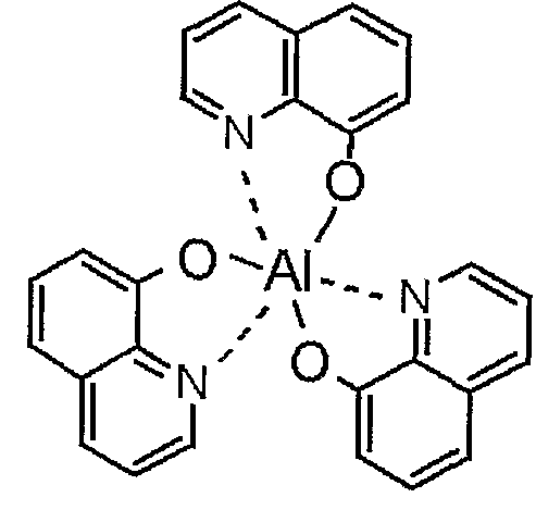
具体的には、 8—ヒドロキシキノリンアルミニウム (A l q 3 ) 、 ァ ントラセン、 ナフタレン、 フエナントレン、 ピレン、 クリセン、 ペリレ ン、 ブタジエン、 クマリン、 ァクリジン、 スチルベン、 又はこれらの誘 導体等が挙げられる。 Specific examples thereof include 8-hydroxyquinoline aluminum (Alq 3 ), anthracene, naphthalene, phenanthrene, pyrene, chrysene, perylene, butadiene, coumarin, acridine, stilbene, and derivatives thereof.
基板 1は、 例えば、 ガラス、 プラスチック等の光透過性の材料を適宣 用いることができる。 また、 他の表示素子と組み合わせて用いる場合や. 第 3図及び第 4図に示した積層構造をマトリックス状に配置する場合等 は、 この基板を共用してもよい。 For the substrate 1, for example, a light-transmitting material such as glass or plastic can be appropriately used. Further, this substrate may be shared when used in combination with another display element, or when the laminated structures shown in FIGS. 3 and 4 are arranged in a matrix.
また、 陽極 2は、 透明電極であり、 I T〇や S n〇2等が使用できる, この陽極 2と正孔輸送層 6 (又は正孔輸送層 1 0 ) との間には、 電荷注 入効率を改善する目的で、 無機物、 有機物もしくは有機金属化合物、 例 えば 2— T N A T A ( 4 , 4, , 4 " ートリス ( 2 一ナフチルフエニル ァミノ) トリフエニルァミン) や、 米国特許第 4 7 2 0 4 3 2号に記載 のポノレフィ リン化合物等 (以下、 同様) からなる薄膜を設けてもよい。 なお、 封止層 4が金属等の導電性材料で形成されている場合は、 陽極 2 の側面に絶縁膜が設けられていてもよい。 The anode 2 is a transparent electrode, can be used IT_〇 or S N_〇 2, etc., between the anode 2 and the hole transport layer 6 (or the hole transport layer 1 0), charge injection inlet In order to improve efficiency, inorganic, organic or organometallic compounds such as 2-TNATA (4,4,, 4 "tris (2-naphthylphenylamino) triphenylamine) and US Pat. No. 4,720,044 32 A thin film made of a ponorefilin compound or the like described in No. 2 (the same applies hereinafter) may be provided.If the sealing layer 4 is formed of a conductive material such as a metal, it may be provided on the side surface of the anode 2. An insulating film may be provided.
また、 有機電界発光素子 Cにおける有機層 5 aは、 正孔輸送層 6と電 子輸送層 7とが積層された有機層であり、 これらのいずれか又は双方に
上記したスチリル化合物を含む混合層として、 発光性の正孔輸送層 6又 は電子輸送層 7を形成してよい。 有機電界発光素子 Dにおける有機層 5 bは、 正孔輸送層 1 0と上記したスチリル化合物を含む混合物からなる 発光層 1 1と電子輸送層 1 2とが積層された有機層であるが、 その他、 種々の積層構造を採ることができる。 例えば、 正孔輸送層と電子輸送層 のいずれか若しくは両方が発光してもよい。 Further, the organic layer 5a in the organic electroluminescent element C is an organic layer in which the hole transport layer 6 and the electron transport layer 7 are laminated, and one or both of them are provided. As a mixed layer containing the above styryl compound, a luminescent hole transporting layer 6 or an electron transporting layer 7 may be formed. The organic layer 5b in the organic electroluminescent device D is an organic layer in which the light emitting layer 11 and the electron transport layer 12 made of a mixture containing the hole transport layer 10 and the styryl compound described above are laminated. Various laminated structures can be adopted. For example, one or both of the hole transport layer and the electron transport layer may emit light.
また、 正孔輸送層において、 正孔輸送性能を向上させるため、 複数種 の正孔輸送材料を積層した正孔輸送層を形成してもよい。 Further, in the hole transport layer, a hole transport layer in which a plurality of types of hole transport materials are stacked may be formed in order to improve hole transport performance.
また、 有機電界発光素子 Cにおいて、 発光層は電子輸送性発光層 7で あってよいが、 電源 8から印加される電圧によっては、 正孔輸送層 6や その界面で発光される場合がある。 同様に、 有機電界発光素子 Dにおい て、 発光層は層 1 1以外に、 電子輸送層 1 2であってもよく、 正孔輸送 層 1 0であってもよい。 発光性能を向上させるため、 少なくとも 1種の 蛍光性材料を用いた発光層 1 1を正孔輸送層と電子輸送層との間に狭持 させた構造であるのがよい。 或いは、 この蛍光性材料を正孔輸送層又は 電子輸送層、 或いはこれら両層に含有させた構造を構成してよい。 この ような場合、 発光効率を改善するために、 正孔又は電子の輸送を制御す るための薄膜 (ホールブロッキング層やエキシトン生成層など) をその 層構成に含ませることも可能である。 In the organic electroluminescent element C, the light emitting layer may be the electron transporting light emitting layer 7, but depending on the voltage applied from the power supply 8, light may be emitted from the hole transporting layer 6 or its interface. Similarly, in the organic electroluminescent element D, the light emitting layer may be the electron transport layer 12 or the hole transport layer 10 other than the layer 11. In order to improve the light emitting performance, it is preferable that the light emitting layer 11 using at least one kind of fluorescent material is sandwiched between the hole transport layer and the electron transport layer. Alternatively, a structure in which this fluorescent material is contained in the hole transporting layer or the electron transporting layer, or both of these layers may be formed. In such a case, in order to improve the luminous efficiency, a thin film (such as a hole blocking layer or an exciton generation layer) for controlling the transport of holes or electrons can be included in the layer configuration.
また、 陰極 3に用いる材料としては、 L i 、 M g、 C a等の活性な金 属と A g、 A l 、 I n等の金属との合金を使用でき、 これらの金属層が 積層した構造であってもよい。 なお、 陰極の厚みや材質を適宜選択する ことによって、 用途に見合った有機電界発光素子を作製できる。 In addition, as a material used for the cathode 3, an alloy of an active metal such as Li, Mg, or Ca and a metal such as Ag, Al, or In can be used, and these metal layers are laminated. It may be a structure. Incidentally, by appropriately selecting the thickness and material of the cathode, an organic electroluminescent device suitable for the intended use can be produced.
また、 封止層 4は、 封止膜として作用するものであり、 有機電界発光 素子全体を覆う構造とすることにより、 電荷注入効率や発光効率を向上 できる。 なお、 その気密性が保たれれば、 アルミニウム、 金、 クロム等
の単金属又は合金や、 酸化シリコン、 窒化シリコン等のシリコン化合物. 有機物など、 適宜その材料を選択できる。 Further, the sealing layer 4 functions as a sealing film, and the charge injection efficiency and the luminous efficiency can be improved by adopting a structure that covers the entire organic electroluminescent element. If the airtightness is maintained, aluminum, gold, chrome, etc. Materials such as single metals or alloys, silicon compounds such as silicon oxide and silicon nitride, and organic substances can be selected as appropriate.
第 5図は、 基板 1上に、 陽極 2と、 正孔輸送層 6と電子輸送層 7とか らなる有機層 5 cと、 透明又は半透明の陰極 3とが順次積層された積層 構造を有し、 この積層構造が封止層 4によって封止されてなる、 シング ルヘテロ構造の上面発光型の有機電界発光素子 Eである。 この場合、 正 孔輸送層 6と電子輸送層 7との界面から、 所定波長の発光光 2 0を発生 し、 この発光は陰極 3又は封止層 4側から観測される。 FIG. 5 shows a laminated structure in which an anode 2, an organic layer 5c composed of a hole transport layer 6 and an electron transport layer 7, and a transparent or translucent cathode 3 are sequentially laminated on a substrate 1. The stacked structure is sealed by a sealing layer 4 to form a top emission type organic electroluminescent element E having a single hetero structure. In this case, emission light 20 of a predetermined wavelength is generated from the interface between the hole transport layer 6 and the electron transport layer 7, and this emission is observed from the cathode 3 or the sealing layer 4 side.
第 6図は、 基板 1上に、 陽極 2と、 正孔注入層 9と正孔輸送層 1 0と 発光層 1 1と電子輸送層 1 2とからなる有機層 5 dと、 透明又 半透明 の陰極 3とが順次積層された積層構造を有し、 この積層構造が封止層 4 によって封止されてなる、 上面発光型の有機電界発光素子 Fである。 こ の有機電界発光素子においても、 第 4図に示した有機電界発光素子と同 様に、 発光層 1 1において、 電子 Z正孔の再結合が生じて励起子が生成 し、 この励起子から所定波長の発光が発生する。 FIG. 6 shows an anode 2, an organic layer 5d composed of a hole injection layer 9, a hole transport layer 10, a light emitting layer 11, and an electron transport layer 12 on a substrate 1, and a transparent or translucent A top emission type organic electroluminescent device F, having a laminated structure in which the cathode 3 is sequentially laminated, and the laminated structure is sealed by a sealing layer 4. Also in this organic electroluminescent device, as in the organic electroluminescent device shown in FIG. 4, recombination of the electron Z hole occurs in the light emitting layer 11 to generate an exciton, and the exciton is generated from the exciton. Light emission of a predetermined wavelength is generated.
上述した各有機電界発光素子 E、 Fにおいて、 基板 1は、 例 ば、 A g、 A u、 A l 、 C r、 I n等、 又はその合金等のような光反射性の材 料を適宜用いることができる、 また、 他の表示素子と組み合わせて用い る場合や、 第 5図及び第 6図に示した積層構造をマトリックス状に配置 する場合等は、 この基板を共用してもよい。 In each of the organic electroluminescent elements E and F described above, the substrate 1 is made of a light-reflective material such as, for example, Ag, Au, Al, Cr, In, or an alloy thereof as appropriate. This substrate may be shared when it can be used, when it is used in combination with another display element, or when the laminated structures shown in FIGS. 5 and 6 are arranged in a matrix.
また、 この基板 1上の陽極 2は、 反射性電極であり、 A g、 A u、 A 1 、 C r、 I n、 又はその合金等を使用でき、 また I T O等を積層して 使用でき、 その厚みは成膜性及び反射性を考慮すると、 5 0 n m以上と するのがよく、 2 0 0 n m以下とすることができる。 こうした陽極を用 いると、 基板 1は上記した光反射性材料に限らず、 ガラス等の透明又は 半透明材料を用いてもよい。
また、 第 6図に示すように、 陽極 2と正孔輸送層 1 0との間には、 電 荷注入効率を改善する目的で、 無機物、 有機物もしくは有機金属化合物 からなる正孔注入層 9を設けてもよい。 又、 図示はしないが、 第 5図に おいても陽極 2と正孔輸送層 6との間には、 前記と同様の正孔注入層 9 を設けてもよい。 なお、 封止層 4が金属等の導電性材料で形成されてい る場合は、 絶縁分離のために、 陽極 2の側面に絶縁膜が設けられていて もよい。 The anode 2 on the substrate 1 is a reflective electrode, and can be Ag, Au, A1, Cr, In, or an alloy thereof, or can be used by laminating ITO or the like. The thickness is preferably not less than 50 nm, and can be not more than 200 nm, in consideration of film formability and reflectivity. When such an anode is used, the substrate 1 is not limited to the light-reflective material described above, but may be a transparent or translucent material such as glass. As shown in FIG. 6, a hole injection layer 9 made of an inorganic, organic, or organometallic compound is provided between the anode 2 and the hole transport layer 10 for the purpose of improving the charge injection efficiency. It may be provided. Although not shown, a hole injection layer 9 similar to the above may be provided between the anode 2 and the hole transport layer 6 in FIG. When the sealing layer 4 is formed of a conductive material such as a metal, an insulating film may be provided on the side surface of the anode 2 for insulation separation.
有機電界発光素子 Eにおける有機層 5 cは、 正孔輸送層 6と電子輸送 層 7とが積層された有機層であり、 これらのいずれか又は双方に上記し たスチリル化合物を含む混合層として、 発光性の正孔輸送層 6又は電子 輸送層 7を形成してよい。 有機電界発光素子 Fにおける有機層 5 dは、 正孔輸送層 1 0と、 上記したスチリル化合物を含む混合物からなる発光 層 1 1と、 電子輸送層 1 2とが積層された有機層であるが、 その他、 種々の積層構造を採ることができる。 例えば、 正孔輸送層と電子輸送層 のいずれか若しくは両方が発光してもよい。 The organic layer 5c in the organic electroluminescent element E is an organic layer in which a hole transport layer 6 and an electron transport layer 7 are laminated, and as a mixed layer containing the styryl compound described above in one or both of them. The luminescent hole transport layer 6 or the electron transport layer 7 may be formed. The organic layer 5 d in the organic electroluminescent element F is an organic layer in which the hole transport layer 10, the light emitting layer 11 composed of a mixture containing the above styryl compound, and the electron transport layer 12 are laminated. Various other laminated structures can be adopted. For example, one or both of the hole transport layer and the electron transport layer may emit light.
また、 正孔輸送層において、 正孔輸送性能を向上させるため、 複数種 の正孔輸送材料を積層した正孔輸送層を形成してもよい。 Further, in the hole transport layer, a hole transport layer in which a plurality of types of hole transport materials are stacked may be formed in order to improve hole transport performance.
また、 有機電界発光素子 Eにおいて、 発光層は電子輸送性発光層 7で あってよいが、 電源 8から印加される電圧によっては、 正孔輸送層 6や その界面で発光される場合がある。 同様に、 有機電界発光素子 Fにおい て、 発光層は層 1 1以外に、 電子輸送層 1 2であってもよく、 正孔輸送 層 1 0であってもよい。 発光性能を向上させるため、 少なくとも 1種の 蛍光性材料を用いた発光層 1 1を正孔輸送層と電子輸送層との間に挟持 させた構造であるのがよい。 或いは、 この蛍光性材料を正孔輸送層又は 電子輸送層、 或いはこれら両層に含有させた構造を構成してよい。 この ような場合、 発光効率を改善するために、 正孔又は電子の輸送を制御す
るための薄膜 (ホールブロッキング層やエキシトン生成層など) をその 層構成に含ませることも可能である。 In the organic electroluminescent device E, the light emitting layer may be the electron transporting light emitting layer 7, but depending on the voltage applied from the power supply 8, light may be emitted from the hole transporting layer 6 or its interface. Similarly, in the organic electroluminescent element F, the light emitting layer may be the electron transport layer 12 or the hole transport layer 10 other than the layer 11. In order to improve the light emitting performance, it is preferable that the light emitting layer 11 using at least one kind of fluorescent material is sandwiched between the hole transport layer and the electron transport layer. Alternatively, a structure in which this fluorescent material is contained in the hole transporting layer or the electron transporting layer, or both of these layers may be formed. In such cases, control of hole or electron transport is used to improve luminous efficiency. It is also possible to include a thin film (such as a hole blocking layer or an exciton generation layer) for the layer structure.
また、 陰極 3に用いる材料としては、 L i、 Mg、 C a等の活性な金 属と Ag、 A l、 I n等の金属との合金を使用でき、 これらの金属層が 積層した構造であってもよい。 なお、 陰極の厚みや材質を適宜選択する ことによって、 用途に見合った有機電界発光素子を作製できるが、 陰極 の厚みは 0. 5〜 1 5 nm、 更には 0. 5〜 5 n m程度が望ましい。 また、 封止層 4は、 封止膜として作用するものであり、 有機電界発光 素子全体を覆う構造とすることにより、 電荷注入効率や発光効率を向上 できる。 なお、 その気密性が保たれれば、 アルミニウム、 金、 クロム、 酸化シリコン、 窒化シリコン等の単金属又は合金、 化合物など、 適宜そ の材料を選択できる。 Further, as a material used for the cathode 3, an alloy of an active metal such as Li, Mg, and Ca and a metal such as Ag, Al, and In can be used, and a structure in which these metal layers are laminated is used. There may be. An organic electroluminescent device suitable for the intended use can be manufactured by appropriately selecting the thickness and material of the cathode, but the thickness of the cathode is preferably 0.5 to 15 nm, and more preferably about 0.5 to 5 nm. . Further, the sealing layer 4 functions as a sealing film, and the charge injection efficiency and the luminous efficiency can be improved by adopting a structure that covers the entire organic electroluminescent element. If the airtightness is maintained, the material can be appropriately selected, such as a single metal such as aluminum, gold, chromium, silicon oxide, or silicon nitride, an alloy, or a compound.
上述した各有機電界発光素子 E、 Fにおいては、 発光層が陽極と陰極 との間に挟持された構造であり、 発光した光は陽極と陰極との間で多重 干渉を生じる。 陽極及び陰極の反射率、 透過率などの光学的な特性と、 これらに挟持された有機層の膜厚とを適当に選ぶことにより、 多重干渉 効果を積極的に利用することができ、 素子 E、 Fより取り出される発光 波長を制御することが可能となる。 これにより、 発光色度を改善するこ とも可能となる。 この多重干渉効果のメカニズムについては、 ; LYamada 等による AM- LCD Digest of Technical Papers, OD-2, 80 (2002)を 参照することができる。 Each of the above-mentioned organic electroluminescent elements E and F has a structure in which the light emitting layer is sandwiched between the anode and the cathode, and the emitted light causes multiple interference between the anode and the cathode. By appropriately selecting the optical characteristics such as the reflectance and transmittance of the anode and the cathode and the thickness of the organic layer sandwiched between them, the multiple interference effect can be positively utilized, and the element E can be used. And F. It is possible to control the emission wavelength extracted from F. As a result, the emission chromaticity can be improved. For the mechanism of this multiple interference effect, reference can be made to AM-LCD Digest of Technical Papers by LYamada et al., OD-2, 80 (2002).
上記した各有機電界発光素子に印加する電流は通常、,直流であるが、 パルス電流や交流を用いてもよい。 電流値、 電圧値は、 素子破壊しない 範囲内であれば特に制限はないが、 有機電界発光素子の消費電力や寿命 を考慮すると、 なるべく小さい電気エネルギーで効率良く発光させるこ とが望ましい。
次に、 第 7図は、 本発明の有機電界発光素子を用いた平面ディスプレ ィの構成例である。 図示の如く、 例えばフルカラ一ディスプレイの場合 は、 赤 (R ) 、 緑 (G ) 及び青 (B ) の 3原色を発光可能な有機層 5 (有機層 5 a , 5 b, 5 c , 5 d ) が、 陰極 3と陽極 2との間に配され ている。 陰極 3及び陽極 2は、 互いに交差するストライプ状に設けるこ とができ、 輝度信号回路 1 4及びシフトレジスタ内蔵の制御回路 1 5に より選択されて、 それぞれに信号電圧が印加され、 これによつて、 選択 された陰極 3及び陽極 2が交差する位置 (画素) の有機層が発光するよ うに構成されている。 The current applied to each of the above-mentioned organic electroluminescent elements is usually a direct current, but a pulse current or an alternating current may be used. The current value and the voltage value are not particularly limited as long as the device does not destroy the device. However, in consideration of the power consumption and the life of the organic electroluminescent device, it is desirable to emit light efficiently with as little electric energy as possible. Next, FIG. 7 shows a configuration example of a planar display using the organic electroluminescent device of the present invention. As shown, for example, in the case of a full color display, an organic layer 5 (organic layers 5a, 5b, 5c, 5d) capable of emitting three primary colors of red (R), green (G) and blue (B) is provided. ) Is disposed between the cathode 3 and the anode 2. The cathode 3 and the anode 2 can be provided in a stripe shape crossing each other, and are selected by the luminance signal circuit 14 and the control circuit 15 with a built-in shift register, and a signal voltage is applied to each of them. Thus, the organic layer at the position (pixel) where the selected cathode 3 and anode 2 intersect is configured to emit light.
即ち、 第 7図は例えば 8 X 3 R G B単純マトリックスであって、 正孔 輸送層と、 発光層及び電子輸送層のいずれか少なくとも一つからなる有 機層 5を陰極 3と陽極 2の間に配設したものである (第 3図又は第 4図. 第 5図又は第 6図参照) 。 陰極と陽極は、 ともにストライプ状にパター ニングするとともに、 互いにマトリックス状に直交させ、 シフトレジス 夕内蔵の制御回路 1 5及び輝度信号回路 1 4により時系列的に信号電圧 を印加し、 その交叉位置で発光するように構成されたものである。 かか る構成の E L素子は、 文字 ·記号等のディスプレイとしては勿論、 画像 再生装置としても使用できる。 また、 陰極 3と陽極 2のストライプ状パ ターンを赤 (R ) 、 緑 (G ) 、 青 (B ) の各色毎に配し、 マルチカラー あるいはフルカラーの全固体型フラットパネルディスプレイを構成する ことが可能となる。 また、 上記の単純マトリックス方式のみならず、 ァ クティブマトリックス方式での駆動も可能である。 That is, FIG. 7 is, for example, an 8 × 3 RGB simple matrix in which a hole transport layer and an organic layer 5 including at least one of a light emitting layer and an electron transport layer are provided between the cathode 3 and the anode 2. (Figure 3 or Figure 4; see Figure 5 or Figure 6). The cathode and anode are both patterned in stripes, are orthogonal to each other in a matrix, and are applied with signal voltages in a time series by the control circuit 15 and the luminance signal circuit 14 incorporated in the shift register. It is configured to emit light. The EL element having such a configuration can be used not only as a display for characters and symbols, but also as an image reproducing device. Also, it is possible to arrange a stripe pattern of the cathode 3 and the anode 2 for each color of red (R), green (G), and blue (B) to constitute a multi-color or full-color all solid-state flat panel display. It becomes possible. In addition to the simple matrix method described above, driving in an active matrix method is also possible.
次に、 本発明の実施例を示すが、 本発明はこれに限定されるものでは ない。 Next, examples of the present invention will be described, but the present invention is not limited thereto.
実施例 1 Example 1
本実施例は、 上述の一般式 [ I ] のスチリル化合物のうち、 下記構造
式 (1 7) — 1 1のアミノスチリル化合物と、 ひ一 NPD (α—ナフチ ルフエ二ルジァミン) との混合層を正孔輸送性発光層として用い、 シン ダルへテロ構造の下面発光型の有機電界発光素子を作製した例である。 構造式 ( 1 7 ) — 1 1 : In this example, among the styryl compounds of the above general formula [I], Using a mixed layer of the aminostyryl compound of formula (17) — 11 and Hiichi NPD (α-naphthylphenyldiamine) as a hole-transporting light-emitting layer, a bottom-emitting organic organic compound having a sindar hetero structure This is an example in which an electroluminescent element is manufactured. Structural formula (17) — 11:
a -NPD: a -NPD:
まず、 真空蒸着装置中に、 1 0 0 nmの厚さの I TOからなる陽極が 一表面に形成された 3 OmmX 3 0 mmのガラス基板をセッティングし た。 蒸着マスクとして複数の 2. 0 mmx 2. Ommの単位開口を有す る金属マスクを基板に近接して配置し、 真空蒸着法により 1 0— 4P a以 下の真空下で上記構造式 ( 1 7) — 1 1のスチリル化合物と正孔輸送材 料である α— N P Dとを重量比 1 : 1で混合した層を例えば 50 nmの 厚さに正孔輸送層 (兼発光層) として成膜した。 蒸着レートは各々 0. 1 nm/秒とした。 First, a 3 Omm × 30 mm glass substrate having an anode made of 100 nm thick ITO formed on one surface was set in a vacuum evaporation apparatus. A plurality of 2. 0 mmx as deposition mask 2. metal mask that having a unit opening disposed close to the substrate Omm, the structural formula in vacuo follows 1 0- 4 P a by vacuum evaporation ( 1 7) — A layer in which the styryl compound of 11 and α-NPD, which is a hole transport material, are mixed at a weight ratio of 1: 1 is formed as a hole transport layer (cum-emitting layer) to a thickness of, for example, 50 nm. Filmed. The deposition rates were each 0.1 nm / sec.
さらに、 電子輸送層材料として下記構造式の A 1 q3 (トリス (8 —
キノリノール) アルミニウム) を正孔輸送層に接して蒸着した。 A l q 3からなるこの電子輸送層の膜厚も例えば 5 0 nmとし、 蒸着レートは 0. 2 nm/秒とした。 Further, as an electron transport layer material, A 1 q 3 (Tris (8— Quinolinol) aluminum) was deposited in contact with the hole transport layer. And the film thickness also for instance 5 0 nm of the electron-transport layer composed of A lq 3, the evaporation rate was 0. 2 nm / sec.
Alq3:
陰極材料としては Mgと Agの混合膜を採用し、 これも蒸着により、 例えば Mgと Agの混合比を 1 : 3として 20 0 nmの厚さに形成し、 実施例 1による第 3図に示した如き有機電界発光素子を作製した。 Alq 3 : As a cathode material, a mixed film of Mg and Ag was adopted, which was also formed by vapor deposition, for example, with a mixture ratio of Mg and Ag of 1: 3 to a thickness of 200 nm, as shown in FIG. 3 according to Example 1. An organic electroluminescent device as described above was produced.
このように作製した実施例 1の有機電界発光素子に、 窒素雰囲気下で 順バイアス直流電圧を加えて発光特性を評価した。 発光色は赤色であり、 分光測定を行った結果、 6 20 nm付近に発光ピークを有するスぺクト ルを得た。 分光測定は、 大塚電子社製のフォトダイオードアレイを検出 器とした分光器を用いた。 また、 電圧一輝度測定を行ったところ、 8 V で 1 5 0 0 c d/m2の輝度が得られた。 To the organic electroluminescent device of Example 1 thus manufactured, a forward bias DC voltage was applied in a nitrogen atmosphere to evaluate the light emitting characteristics. It emitted red light. By spectral analysis, a spectrum having a light emission peak at about 620 nm was obtained. For spectrometry, a spectrometer using a photodiode array made by Otsuka Electronics Co., Ltd. as a detector was used. In addition, when the voltage-brightness measurement was performed, a luminance of 1500 cd / m 2 was obtained at 8 V.
この有機電界発光素子を作製後、 窒素雰囲気下に 1ヶ月間放置したが、 素子劣化は観察されなかった。 また、 初期輝度 30 0 c dZm2で電流 値を一定に通電して連続発光し、 強制劣化させた際、 輝度が半減するま で 2 5 0 0時間であった。 After fabrication of this organic electroluminescent device, the device was left under a nitrogen atmosphere for one month, but no device degradation was observed. Further, by passing current value at an initial luminance 30 0 c DZM 2 constant continuous light emission, when the forced deterioration, luminance was 2 5 0 0 hour half until.
実施例 2 Example 2
本実施例は、 上述の一般式 [I]のスチリル化合物のうち、 上記構造式 ( 1 7) 一 1 1のスチリル化合物と、 上記構造式の A 1. q3との混合層
を電子輸送性発光層として用い、 シングルヘテロ構造の下面発光型の有 機電界発光素子を作製した例である。 This embodiment, of the styryl compound of the above general formula [I], the structural formula (1 7) one 1 1 styryl compound, mixed layer of A 1. q 3 of the structural formula This is an example in which a bottom emission type organic electroluminescent element having a single hetero structure was manufactured by using as an electron transporting light emitting layer.
まず、 真空蒸着装置中に、 1 0 0 nmの厚さの I TOからなる陽極が 一表面に形成された 3 OmmX 3 0 mmのガラス基板をセッティングし た。 蒸着マスクとして複数の 2. 0 mmX 2. 0mmの単位開口を有す る金属マスクを基板に近接して配置し、 真空蒸着法により 1 0— 4 P a以 下の真空下で前記構造式のひ一 NPDを例えば 5 0 nmの厚さに成膜し た。 蒸着レートは 0. I nmZ秒とした。 First, a 3 Omm × 30 mm glass substrate having an anode made of 100 nm thick ITO formed on one surface was set in a vacuum evaporation apparatus. A plurality of metal masks having a unit opening of 2.0 mm × 2.0 mm as a vapor deposition mask are arranged in close proximity to the substrate, and a vacuum vapor deposition method is used under the vacuum of 10 to 4 Pa or less to form the above structural formula. Hiichi NPD was deposited to a thickness of, for example, 50 nm. The deposition rate was 0.1 nmZ seconds.
さらに、 上記構造式 ( 1 7) — 1 1のスチリル化合物と電子輸送性材 料である A 1 q3とを重量比 1 : 1で混合した層を正孔輸送層に接して 蒸着した。 上記構造式 (1 7) — 1 1のアミノスチリル化合物と A 1 q 3とからなる電子輸送層 (兼発光層) の膜厚も例えば 50 nmとし、 蒸 着レートは各々 0. 2 nm/秒とした。 Furthermore, the structural formula (1-7) - 1 1 styryl compound and the electron-transporting materials in which A 1 q 3 and the weight ratio of 1: mixed layer of was deposited in contact with the hole transport layer at 1. The structural formula (1-7) - 1 1 and the film thickness also for instance 50 nm of aminostyryl compound and the electron-transporting layer composed of A 1 q 3 Tokyo (and light emitting layer), deposited rates each 0. 2 nm / sec And
陰極材料としては M gと A gの混合膜を採用し、 これも蒸着により、 例えば Mgと A gの混合比を 1 : 3として 2 0 0 nmの厚さに形成し、 実施例 2による第 3図に示した如き有機電界発光素子を作製した。 As the cathode material, a mixed film of Mg and Ag was employed, and this was also formed by vapor deposition to a thickness of 200 nm, for example, with a mixing ratio of Mg and Ag of 1: 3. An organic electroluminescent device as shown in FIG. 3 was produced.
このように作製した実施例 2の有機電界発光素子に、 窒素雰囲気下で 順バイアス直流電圧を加えて発光特性を評価した。 発光色は赤色であり、 実施例 1と同様に分光測定を行った結果、 6 2 0 nm付近に発光ピーク を有するスペクトルを得た。 また、 電圧—輝度測定を行ったところ、 8 Vで 2 6 0 0 c d/m2の輝度が得られた。 The organic electroluminescent device of Example 2 fabricated in this manner was evaluated for luminous characteristics by applying a forward bias DC voltage under a nitrogen atmosphere. It emitted a red light, which was found by spectrometry (as in Example 1) to have a peak at about 60 nm. In addition, when voltage-luminance measurement was performed, a luminance of 260 cd / m 2 was obtained at 8 V.
この有機電界発光素子を作製後、 窒素雰囲気下に 1ヶ月間放置したが、 素子劣化は観察されなかった。 また、 初期輝度 3 0 0 c d/m2で電流 値を一定に通電して連続発光し、 強制劣化させた際、 輝度が半減するま で 2 7 0 0時間であった。 After fabrication of this organic electroluminescent device, the device was left under a nitrogen atmosphere for one month, but no device degradation was observed. In addition, when the current value was kept constant at an initial luminance of 300 cd / m 2 to continuously emit light and was forcibly deteriorated, it took 270 hours until the luminance was reduced by half.
実施例 3 ·
本実施例は、 上述の一般式 [I ]のスチリル化合物のうち、 上記構造式 ( 1 7) - 1 1のスチリル化合物と、 上記構造式の A 1 q3との混合層 を電子輸送性発光層として用い、 ダブルへテロ構造の下面発光型の有機 電界発光素子を作製した例である。 Example 3 This embodiment, of the styryl compound of the above general formula [I], the structural formula (1-7) - 1 1 of the styryl compound, mixed layer electron transport light-emitting of the A 1 q 3 of the structural formula This is an example in which a bottom emission type organic electroluminescent device having a double hetero structure was used as a layer.
まず、 真空蒸着装置中に、 1 0 0 nmの厚さの I TOからなる陽極が 一表面に形成された 3 OmmX 3 0 mmのガラス基板をセッティングし た。 蒸着マスクとして複数の 2. 0 mmX 2. 0mmの単位開口を有す る金属マスクを基板に近接して配置し、 真空蒸着法により 10— 4 P a以 下の真空下で上記構造式の at— NPDを例えば 30 nmの厚さに成膜し た。 蒸着レートは 0. 2 nmZ秒とした。 First, a 3 Omm × 30 mm glass substrate having an anode made of 100 nm thick ITO formed on one surface was set in a vacuum evaporation apparatus. A metal mask that having a plurality of 2. 0 mmX 2. unit openings 0mm as deposition mask arranged close to the substrate, under a vacuum of 10- 4 P a hereinafter by vacuum deposition of the structural formula at — NPD was deposited to a thickness of, for example, 30 nm. The deposition rate was 0.2 nmZ seconds.
さらに、 発光材料として上記構造式 ( 1 7) — 1 1のスチリル化合物 と A l q3とを重量比 1 : 1で正孔輸送層に接して蒸着した。 上記構造 式 ( 1 7) — 1 1のスチリル化合物と A 1 q3との混合層からなる発光 層の膜厚も例えば 30 nmとし、 蒸着レートは各々 0. 2 nmZ秒とし た。 Furthermore, the structural formula (1 7) as the light emitting material - 1 1 styryl compound A lq 3 and the weight ratio of 1: was deposited in contact with the hole transport layer at 1. The structural formula (1-7) - 1 1 and the film thickness also for instance 30 nm light-emitting layer comprising a mixed layer of styryl compound and A 1 q 3, the deposition rate was at each 0. 2 NMZ seconds.
さらに、 電子輸送性材料として上記構造式の A 1 d3を発光層に接し て蒸着した。 A 1 q3の膜厚を例えば 3 0 nmとし、 蒸着レートは 0.Further, A 1 d 3 of the above structural formula was deposited as an electron transporting material in contact with the light emitting layer. The thickness of A 1 q 3 is , for example, 30 nm, and the deposition rate is 0.
2 nm/秒とした。 2 nm / sec.
陰極材料としては M gと A gの混合膜を採用し、 これも蒸着により、 例えば Mgと Agの混合比を 1 : 3として 20 0 nmの厚さに形成し、 実施例 3による第 4図に示した如き有機電界発光素子を作製した。 As a cathode material, a mixed film of Mg and Ag was adopted, and this was also formed by vapor deposition, for example, with a mixing ratio of Mg and Ag of 1: 3 to a thickness of 200 nm. The organic electroluminescent device as shown in was manufactured.
このように作製した実施例 3の有機電界発光素子に、 窒素雰囲気下で 順バイアス直流電圧を加えて発光特性を評価した。 発光色は赤色であり、 実施例 1と同様に分光測定を行った結果、 6 2 0 nmに発光ピークを有 するスペクトルを得た。 また、 電圧一輝度測定を行ったところ、 8 Vで The organic electroluminescent device of Example 3 thus manufactured was evaluated by applying a forward bias DC voltage under a nitrogen atmosphere to evaluate the light emitting characteristics. It emitted red light, which was found by spectrometry (as in Example 1) to have a peak at 60 nm. When voltage-brightness measurement was performed,
3 2 0 0 c dZm2の輝度が得られた。
この有機電界発光素子を作製後、 窒素雰囲気下に 1ヶ月間放置したが、 素子劣化は観察されなかった。 また、 初期輝度 30 0 c d/m2で電流 値を一定に通電して連続発光して強制劣化させた際、 輝度が半減するま で 3 50 0時間であった。 3 2 0 0 luminance of c DZM 2 was obtained. After fabrication of this organic electroluminescent device, the device was left under a nitrogen atmosphere for one month, but no device degradation was observed. In addition, when the current was continuously supplied at an initial luminance of 300 cd / m 2 and the light was continuously emitted and forcedly deteriorated, it took 350 hours until the luminance was reduced by half.
実施例 4 Example 4
本実施例は、 上述の一般式 [I ]のスチリノレ化合物のうち、 上記構造式 In this example, among the styrenole compounds of the above general formula [I],
(1 7) - 1 1のスチリル化合物と、 下記構造式 ( 1 7) — 1のスチリ ル化合物との混合層を発光層として用い、 ダブルへテロ構造の下面発光 型の有機電界発光素子を作製した例である。 Using a mixed layer of a styryl compound of (1 7) -11 and a styryl compound of the following structural formula (1 7) -1 as a light emitting layer, a bottom emission type organic electroluminescent device having a double hetero structure is manufactured. This is an example.
構造式 ( 1 7) — 1 : Structural formula (1 7) — 1:
まず、 真空蒸着装置中に、 1 0 0 nmの厚さの I TOからなる陽極が 一表面に形成された 30 mmx 3 0 mmのガラス基板をセッティングし た。 蒸着マスクとして複数の 2. 0 mmX 2. 0mmの単位開口を有す る金属マスクを基板に近接して配置し、 真空蒸着法により 1 0— 4 P a以 下の真空下で上記構造式の 一 NPDを例えば 30 nmの厚さに成膜し た。 蒸着レートは 0. 2 nmZ秒とした。 First, a 30 mm × 30 mm glass substrate on which an anode made of 100 nm thick ITO was formed on one surface was set in a vacuum evaporation apparatus. A plurality of metal masks each having a unit opening of 2.0 mm X 2.0 mm are placed in close proximity to the substrate as a vapor deposition mask, and the above-mentioned structural formula is formed by a vacuum vapor deposition method under a vacuum of 10 to 4 Pa or less. One NPD was formed to a thickness of, for example, 30 nm. The deposition rate was 0.2 nmZ seconds.
さらに、 発光材料として上記構造式 ( 1 7) — 1 1のスチリル化合物 と上記構造式 (1 7) — 1のスチリル化合物とを重量比 1 : 3で正孔輸 送層に接して共蒸着した。 上記構造式 ( 1 7) — 1 1のスチリル化合物 と上記構造式 (1 7) — 1のスチリル化合物との混合層からなる発光層 の膜厚も例えば 3 0 nmとし、 蒸着レート 上記構造式 (1 7) — 1 1
の化合物は 0. I nmZ秒、 上記構造式 (17) — 1の化合物は 0. 3 n m/秒とした。 Further, as a light emitting material, a styryl compound of the above structural formula (17) -11 and a styryl compound of the above structural formula (17) -1 were co-evaporated in contact with the hole transport layer at a weight ratio of 1: 3. . The thickness of the light-emitting layer composed of a mixed layer of the styryl compound of the above structural formula (17) —11 and the styryl compound of the above structural formula (17) —1 is also set to, for example, 30 nm. 1 7) — 1 1 The compound of formula (1) was 0.3 nm / sec, and the compound of formula (17) -1 was 0.3 nm / sec.
さらに、 電子輸送性材料として上記構造式の A 1 d3を発光層に接し て蒸着した。 A 1 d3の膜厚を例えば 30 nmとし、 蒸着レートは 0. 2 nm/秒とした。 Further, A 1 d 3 of the above structural formula was deposited as an electron transporting material in contact with the light emitting layer. The film thickness of A 1 d 3 was , for example, 30 nm, and the deposition rate was 0.2 nm / sec.
陰極材料としては Mgと A gの混合朦を採用し、 これも蒸着により、 例えば M gと A gの混合比を 1 : 3として 200 nmの厚さに形成し、 実施例 4による第 4図に示した如き有機電界発光素子を作製した。 As a cathode material, a mixture of Mg and Ag was adopted, and this was also formed by vapor deposition to a thickness of 200 nm, for example, with a mixture ratio of Mg and Ag of 1: 3. The organic electroluminescent device as shown in was manufactured.
このように作製した実施例 4の有機電界発光素子に、 窒素雰囲気下で 順バイアス直流電圧を加えて発光特性を評価した。 発光色は橙色であり, 実施例 1と同様に分光測定を行った結果、 610 nmに発光ピークを有 するスペクトルを得た。 電圧—輝度測定を行ったところ、 8 Vで 220 0 c dZm2の輝度が得られた。 The organic electroluminescent device of Example 4 thus manufactured was evaluated by applying a forward bias DC voltage under a nitrogen atmosphere to evaluate the light emitting characteristics. It emitted an orange light, which was found by spectrometry (as in Example 1) to have a peak at 610 nm. A voltage-luminance measurement showed a luminance of 2200 cdZm 2 at 8 V.
この有機電界発光素子を作製後、 窒素雰囲気下に 1ヶ月間放置したが、 素子劣化は観察されなかった。 また、 初期輝度 300 c dZm2で電流 値を一定に通電して連続発光して強制劣化させた際、 輝度が半減するま で 1000時間であった。 After fabrication of this organic electroluminescent device, the device was left under a nitrogen atmosphere for one month, but no device degradation was observed. Further, when a current value at an initial luminance 300 c DZM 2 forcibly deteriorated continuously emit light by energizing the constant luminance was 1000 hours with a half until.
実施例 5 Example 5
本実施例は、 上述の一般式 [I]のスチリル化合物のうち、 上記構造式 ( 1 7) 一 1のスチリル化合物と、 上記構造式の A 1 Q3との混合層を 電子輸送性発光層として用い、 シングルヘテロ構造の下面発光型の有機 電界発光素子を作製した例である。 This embodiment, of the styryl compound of the above general formula [I], the structural formula (1 7) one 1 of styryl compound and an electron transporting luminescent layer a mixed layer of A 1 Q 3 of the structural formula This is an example in which a bottom emission type organic electroluminescent device having a single hetero structure was manufactured.
層構造、 成膜法とも実施例 2に準拠して有機電界発光素子を作製した このように作製した実施例 5の有機電界発光素子に、 窒素雰囲気下で 順バイアス直流電圧を加えて発光特性を評価した。 発光色は橙色であり、 実施例 1と同様に分光測定を行った結果、 608 nm付近に発光ピーク
を有するスペクトルを得た。 また、 電圧—輝度測定を行ったところ、 8 Vで 1000 c d/m2の輝度が得られた。 An organic electroluminescent device was manufactured according to Example 2 in both the layer structure and the film forming method. The organic electroluminescent device of Example 5 thus manufactured was applied with a forward bias DC voltage in a nitrogen atmosphere to improve the light emitting characteristics. evaluated. The luminescent color is orange. As a result of performing a spectral measurement in the same manner as in Example 1, the luminescent peak is around 608 nm. Was obtained. When voltage-luminance measurement was performed, a luminance of 1000 cd / m 2 was obtained at 8 V.
この有機電界発光素子を作製後、 窒素雰囲気下に 1ヶ月間放置したが、 素子劣化は観察されなかった。 また、 初期輝度 300 c d/m2で電流 値を一定に通電して連続発光し、 強制劣化させた際、 輝度が半減するま で 800時間であった。 After fabrication of this organic electroluminescent device, the device was left under a nitrogen atmosphere for one month, but no device degradation was observed. In addition, when a constant current was applied at an initial luminance of 300 cd / m 2 and continuous light emission was performed and forced deterioration was performed, it took 800 hours for the luminance to decrease to half.
実施例 6 Example 6
本実施例は、 上述の一般式 [I ]のスチリル化合物のうち、 下記構造式 ( 1 7) 一 2のスチリル化合物と、 上記構造式の A 1 Q3との混合層を 電子輸送性発光層として用い、 シングルヘテロ構造の下面発光型の有機 電界発光素子を作製した例である。 構造式 (17) 2 In this example, among the styryl compounds of the above general formula [I], a mixed layer of a styryl compound of the following structural formula (17) 12 and A 1 Q 3 of the above structural formula was used as an electron transporting light emitting layer. This is an example in which a bottom emission type organic electroluminescent device having a single hetero structure was manufactured. Structural formula (17) 2
層構造、 成膜法とも実施例 2に準拠して有機電界発光素子を作製した このように作製した実施例 6の有機電界発光素子に、 窒素雰囲気下で 順バイアス直流電圧を加えて発光特性を評価した。 発'光色は橙色であり、 実施例 1と同様に分光測定を行った結果、 6 1 O nm付近に発光ピーク を有するスペクトルを得た。 また、 電圧一輝度測定を行ったところ、 8 Vで 500 c d/m2の輝度が得られた。 An organic electroluminescent device was fabricated according to Example 2 in both the layer structure and the film forming method. The organic electroluminescent device of Example 6 fabricated as described above was applied with a forward bias DC voltage in a nitrogen atmosphere to improve the luminescent characteristics. evaluated. The emitted light was orange, and the spectrum was measured in the same manner as in Example 1. As a result, a spectrum having an emission peak near 61 O nm was obtained. Voltage-brightness measurement showed a luminance of 500 cd / m 2 at 8 V.
この有機電界発光素子を作製後、 窒素雰囲気下に 1ヶ月間放置したが、 素子劣化は観察されなかった。 また、 初期輝度 300 c dZm2で電流
値を一定に通電して連続発光し、 強制劣化させた際、 輝度が半減するま で 700時間であった。 After fabrication of this organic electroluminescent device, the device was left under a nitrogen atmosphere for one month, but no device degradation was observed. The current at an initial luminance 300 c DZM 2 When a constant value was applied and continuous light emission was performed and forced degradation occurred, it took 700 hours for the luminance to decrease by half.
実施例 7 Example 7
本実施例は、 上述の一般式 [I ]のスチリル化合物のうち、 下記構造式 In this example, among the styryl compounds of the above general formula [I], the following structural formula
( 1 7) 一 3のスチリル化合物と、 上記構造式の A 1 q3との混合層を 電子輸送性発光層として用い、 シングルヘテロ構造の下面発光型の有機 電界発光素子を作製した例である。 (17) This is an example in which a mixed layer of a 13 styryl compound and A 1 q 3 of the above structural formula was used as an electron-transporting light-emitting layer to produce a single-heterostructure bottom-emitting organic electroluminescent device. .
構造式 (1 7) — 3 : Structural formula (1 7) — 3:
層構造、 成膜法とも実施例 2に準拠して有機電界発光素子を作製した < このように作製した実施例 7の有機電界発光素子に、 窒素雰囲気下で 順バイアス直流電圧を加えて発光特性を評価した。 発光色は橙色であり. 実施例 1と同様に分光測定を行った結果、 6 0 5 nm付近に発光ピーク を有するスペクトルを得た。 また、 電圧一輝度測定を行ったところ、 8 An organic electroluminescent device was manufactured in accordance with Example 2 for both the layer structure and the film forming method. <The organic EL device of Example 7 manufactured in this manner was subjected to a forward bias DC voltage in a nitrogen atmosphere under a nitrogen atmosphere to emit light. Was evaluated. The luminescent color was orange. As a result of spectral measurement in the same manner as in Example 1, a spectrum having a luminescent peak near 605 nm was obtained. When voltage-brightness measurement was performed, 8
Vで 1 20 0 c dZm2の輝度が得られた。 A luminance of 1200 cd dZm 2 was obtained at V.
この有機電界発光素子を作製後、 窒素雰囲気下に 1ヶ月間放置したが, 素子劣化は観察されなかった。 また、 初期輝度 3 0 0 c dZm2で電流 値を一定に通電して連続発光し、 強制劣化させた際、 輝度が半減するま で 1 1 0 0時間であった。 After fabrication of this organic electroluminescent device, it was left under a nitrogen atmosphere for one month, but no device degradation was observed. In addition, when the current value was kept constant at an initial luminance of 300 cd dZm 2 to continuously emit light and was forcibly deteriorated, it took 110 hours until the luminance was reduced by half.
実施例 8 Example 8
本実施例は、 上述の一般式 [I]のスチリル化合物のうち、 下記構造式 ( 1 7) 一 4のスチリル化合物と、 上記構造式の A 1 q3との混合層を
電子輸送性発光層として用い、 瞎造の下面発光型の有機 電界発光素子を作製した例である。 In the present example, a mixed layer of the styryl compound of the following structural formula (17) 14 among the styryl compounds of the above general formula [I] and A 1 q 3 of the above structural formula was used. This is an example in which a bottom-emitting organic electroluminescent device made of silicon is used as an electron transporting light emitting layer.
構造式 (1 7) - 4 : Structural formula (1 7)-4:
層構造、 成膜法とも実施例 2に準拠して有機電界発光素子を作製した t このように作製した実施例 8の有機電界発光素子に、 窒素雰囲気下で 順バイアス直流電圧を加えて発光特性を評価した。 発光色は橙色であり、 実施例 1と同様に分光測定を行った結果、 6 0 0 nm付近に発光ピーク を有するスペクトルを得た。 また、 電圧—輝度測定を行ったところ、 8 Vで 1 0 0 0 c dZm2の輝度が得られた。 Layer structure, the organic electroluminescent device of Example 8 in which both film forming method in conformity with Example 2 was prepared like this t fabricated organic electroluminescent device, the light emitting characteristics by applying a forward bias DC voltage in a nitrogen atmosphere Was evaluated. It emitted an orange light, which was found by spectrometry (as in Example 1) to have a peak at about 600 nm. In addition, when voltage-luminance measurement was performed, a luminance of 1000 cdZm 2 was obtained at 8 V.
この有機電界発光素子を作製後、 窒素雰囲気下に 1ヶ月間放置したが、 素子劣化は観察されなかった。 また、 初期輝度 300 c d/m2で電流 値を一定に通電して連続発光し、 強制劣化させた際、 輝度が半減するま で 1 40 0時間であった。 After fabrication of this organic electroluminescent device, the device was left under a nitrogen atmosphere for one month, but no device degradation was observed. In addition, when current was supplied at a constant value at an initial luminance of 300 cd / m 2 and continuous light emission was performed and forced deterioration was performed, it took 1400 hours until the luminance was reduced by half.
実施例 9 Example 9
本実施例は、 上述の一般式 [I ]のスチリル化合物のうち、 下記構造式 ( 1 7) 一 5のスチリル化合物と、 上記構造式の A 1 Q3との混合層を 電子輸送性発光層として用い、 シングルヘテロ構造の下面発光型の有機 電界発光素子を作製した例である。
構造式 ( 1 7) 5 : This embodiment, of the styryl compound of the above general formula [I], the following structural formula (1 7) one 5 styryl compound and an electron transporting luminescent layer a mixed layer of A 1 Q 3 of the structural formula This is an example in which a bottom emission type organic electroluminescent device having a single hetero structure was manufactured. Structural formula (1 7) 5:
層構造、 成膜法とも実施例 2に準拠して有機電界発光素子を作製した t このように作製した実施例 9の有機電界発光素子に、 窒素雰囲気下で 川頁バイアス直流電圧を加えて発光特性を評価した。 発光色は橙色であり、 実施例 1と同様に分光測定を行った結果、 6 1 5 nm付近に発光ピーク を有するスペクトルを得た。 また、 電圧—輝度測定を行ったところ、 8 Vで 9 0 0 c dZm2の輝度が得られた。 Layer structure, the organic electroluminescent device of Example 9 in which both film forming method in conformity with Example 2 was produced as the t fabricated organic electroluminescent device, light emission by adding Kawapeji bias dc voltage in a nitrogen atmosphere The properties were evaluated. It emitted an orange light, which was found by spectrometry (as in Example 1) to have a peak at about 615 nm. In addition, when voltage-luminance measurement was performed, a luminance of 900 cdZm 2 was obtained at 8 V.
この有機電界発光素子を作製後、 窒素雰囲気下に 1ヶ月間放置したが, 素子劣化は観察されなかった。 また、 初期輝度 3 0 0 c dZm2で電流 値を一定に通電して連続発光し、 強制劣化させた際、 輝度が半減するま で 8 5 0時間であった。 After fabrication of this organic electroluminescent device, it was left under a nitrogen atmosphere for one month, but no device degradation was observed. In addition, when a constant current value was applied at an initial luminance of 300 cd dZm 2 to continuously emit light and was forcibly deteriorated, it took 850 hours until the luminance was reduced by half.
実施例 1 0 Example 10
本実施例は、 上述の一般式 [I ]のスチリル化合物のうち、 下記構造式 ( 1 7) 一 6のスチリル化合物と、 上記構造式の A 1 Q3との混合層を 電子輸送性発光層として用い、 シングルヘテロ構造の下面発光型の有機 電界発光素子を作製した例である。 In this example, among the styryl compounds of the above general formula [I], a mixed layer of a styryl compound of the following structural formula (17) 16 and A 1 Q 3 of the above structural formula was used as an electron transporting light emitting layer. This is an example in which a bottom emission type organic electroluminescent device having a single hetero structure was manufactured.
構造式 ( 1 7) - 6 : Structural formula (17) -6:
層構造、 成膜法とも実施例 2に準拠して有機電界発光素子を'作製した。 このように作製した実施例 1 0の有機電界発光素子に、 窒素雰囲気下 で順バイアス直流電圧を加えて発光特性を評価した。 発光色は赤色であ り、 実施例 1と同様に分光測定を行った結果、 620 nm付近に発光ピ —クを有するスペクトルを得た。 また、 電圧一輝度測定を行ったところ、 8 Vで 80 0 c d/m2の輝度が得られた。 An organic electroluminescent device was manufactured according to Example 2 for both the layer structure and the film forming method. A forward bias DC voltage was applied to the organic electroluminescent device of Example 10 thus manufactured in a nitrogen atmosphere to evaluate the light emitting characteristics. It emitted a red light, which was found by spectrometry (as in Example 1) to have a peak at about 620 nm. Voltage-brightness measurement showed a luminance of 800 cd / m 2 at 8 V.
この有機電界発光素子を作製後、 窒素雰囲気下に 1ヶ月間放置したが、 素子劣化は観察されなかった。 また、 初期輝度 30 0 c d/m2で電流 値を一定に通電して連続発光し、 強制劣化させた際、 輝度が半減するま で 7 0 0時間であった。 After fabrication of this organic electroluminescent device, the device was left under a nitrogen atmosphere for one month, but no device degradation was observed. In addition, when the current value was kept constant at an initial luminance of 300 cd / m 2 to continuously emit light and was forcibly degraded, it took 700 hours until the luminance was reduced by half.
実施例 1 1 Example 11
本実施例は、 上述の一般式 [I]のスチリル化合物のうち、 下記構造式 This example shows that among the styryl compounds of the above general formula [I], the following structural formula
(1 7) 一 7のスチリル化合物と、 上記構造式の A 1 q3との混合層を 電子輸送性発光層として用い、 シングルヘテロ構造の下面発光型の有機 電界発光素子を作製した例である。 (17) This is an example in which a mixed layer of the styryl compound of No. 7 and A 1 q 3 of the above structural formula was used as the electron-transporting light-emitting layer to produce a bottom emission type organic electroluminescence device having a single hetero structure. .
構造式 ( 1 7) - 7 : Structural formula (17) -7:
層構造、 成膜法とも実施例 2に準拠して有機電界発光素子を作製した このように作製した実施例 1 1の有機電界発光素子に、 窒素雰囲気下 で順バイアス直流電圧を加えて発光特性を評価した。 発光色は橙色であ り、 実施例 1と同様に分光測定を行った結果、 6 1 5 nm付近に発光ピ ークを有するスペクトルを得た。 また、 電圧—輝度測定を行ったところ,
8 Vで 1 100 c d/m2の輝度が得られた。 An organic electroluminescent device was manufactured in accordance with Example 2 in both the layer structure and the film forming method. The organic electroluminescent device of Example 11 thus manufactured was applied with a forward bias DC voltage in a nitrogen atmosphere to emit light. Was evaluated. It emitted an orange light, which was found by spectrometry (as in Example 1) to have a peak at about 615 nm. Also, when the voltage-luminance measurement was performed, At 8 V, a luminance of 1100 cd / m 2 was obtained.
この有機電界発光素子を作製後、 窒素雰囲気下に 1ヶ月間放置したが 素子劣化は観察されなかった。 また、 初期輝度 300 c d/m2で電流 値を一定に通電して連続発光し、 強制劣化させた際、 輝度が半減するま で 1000時間であった。 After fabrication of this organic electroluminescent device, the device was left under a nitrogen atmosphere for one month, but no device degradation was observed. In addition, when a constant current value was applied at an initial luminance of 300 cd / m 2 and continuous light emission was performed and forced deterioration was performed, it took 1000 hours until the luminance was reduced by half.
実施例 12 Example 12
本実施例は、 上述の一般式 [I ]のスチリル化合物のうち、 下記構造式 In this example, among the styryl compounds of the above general formula [I], the following structural formula
( 1 7) 一 8のスチリル化合物と、 上記構造式の A 1 q3との混合層を 電子輸送性発光層として用い、 シングルヘテロ構造の下面発光型の有機 電界発光素子を作製した例である。 (17) This is an example in which a mixed layer of the styryl compound of No. 18 and A 1 q 3 of the above structural formula was used as an electron transporting light emitting layer to produce a bottom emission type organic electroluminescent device having a single hetero structure. .
構造式 (17) — 8 : Structural formula (17) — 8:
層構造、 成膜法とも実施例 2に準拠して有機電界発光素子を作製した。 このように作製した実施例 12の有機電界発光素子に、 窒素雰囲気下 で順バイァス直流電圧を加えて発光特性を評価した。 発光色は橙色であ り、 実施例 1と同様に分光測定を行った結果、 610 nm付近に発光ピ ークを有するスペクトルを得た。 また、 電圧一輝度測定を行ったところ、 8 Vで 950 c d/m2の輝度が得られた。 An organic electroluminescent device was manufactured according to Example 2 for both the layer structure and the film forming method. To the organic electroluminescent device of Example 12 thus manufactured, a forward bias DC voltage was applied in a nitrogen atmosphere to evaluate the light emitting characteristics. It emitted an orange light, which was found by spectrometry (as in Example 1) to have a peak at about 610 nm. Voltage-brightness measurement showed a luminance of 950 cd / m 2 at 8 V.
この有機電界発光素子を作製後、 窒素雰囲気下に 1ヶ月間放置したが、 素子劣化は観察されなかった。 また、 初期輝度 300 c dZm2で電流 値を一定に通電して連続発光し、 強制劣化させた際、 輝度が半減するま で 1 300時間であった。
実施例 1 3 After fabrication of this organic electroluminescent device, the device was left under a nitrogen atmosphere for one month, but no device degradation was observed. Further, initial luminance 300 by applying a constant current in c DZM 2 to emit light continuously when the forced deterioration, luminance was 1 300 hours with a half until. Example 13
本実施例は、 上述の一般式 [I]のスチリル化合物のうち、 下記構造式 ( 1 7) 一 9のスチリル化合物と、 上記構造式の A 1 q3との混合層を 電子輸送性発光層として用い、 シングルヘテロ構造の下面発光型の有機 電界発光素子を作製した例である。 This embodiment, of the styryl compound of the above general formula [I], the following structural formula (1 7) Single 9 styryl compound and an electron transporting luminescent layer a mixed layer of A 1 q 3 of the structural formula This is an example in which a bottom emission type organic electroluminescent device having a single hetero structure was manufactured.
構造式 (1 7) — 9 : Structural formula (1 7) — 9:
層構造、 成膜法とも実施例 2に準拠して有機電界発光素子を作製した ( このように作製した実施例 1 3の有機電界発光素子に、 窒素雰囲気下 で順バイアス直流電圧を加えて発光特性を評価した。 発光色は橙色であ り、 実施例 1と同様に分光測定を行った結果、 6 0 5 nm付近に発光ピ ークを有するスペクトルを得た。 また、 電圧一輝度測定を行ったところ, 8 Vで 8 5 0 c d/m2の輝度が得られた。 An organic electroluminescent device was fabricated according to Example 2 for both the layer structure and the film forming method. ( The organic electroluminescent device of Example 13 fabricated in this manner was illuminated by applying a forward bias DC voltage under a nitrogen atmosphere. The emission color was orange, and the spectroscopic measurement was performed in the same manner as in Example 1. As a result, a spectrum having a light emission peak near 605 nm was obtained. As a result, a luminance of 850 cd / m 2 was obtained at 8 V.
この有機電界発光素子を作製後、 窒素雰囲気下に 1ヶ月間放置したが、 素子劣化は観察されなかった。 また、 初期輝度 3 0 0 c d/m2で電流 値を一定に通電して連続発光し、 強制劣化させた際、 輝度が半減するま で 6 50時間であった。 After fabrication of this organic electroluminescent device, the device was left under a nitrogen atmosphere for one month, but no device degradation was observed. In addition, when a constant current value was applied at an initial luminance of 300 cd / m 2 to continuously emit light, and the light was forcibly degraded, it took 650 hours until the luminance was reduced by half.
実施例 14 Example 14
本実施例は、 上述の一般式 [I]のスチリル化合物のうち、 下記構造式 ( 1 7) 一 1 0のスチリル化合物と、 上記構造式の A 1 d3との混合層 を電子輸送性発光層として用い、 シングルヘテロ構造の下面発光型の有 機電界発光素子を作製した例である。
構造式 (1 7) - 1 0 : This embodiment, of the styryl compound of the above general formula [I], the following structural formula (1 7) and one 1 0 styryl compounds, mixed layer electron transport light-emitting of the A 1 d 3 of the structural formula This is an example in which a bottom emission type organic electroluminescent element having a single hetero structure was used as a layer. Structural formula (1 7)-10:
層構造、 成膜法とも実施例 2に準拠して有機電界発光素子を作製した c このように作製した実施例 14の有機電界発光素子に、 窒素雰囲気下 で順バイアス直流電圧を加えて発光特性を評価した。 発光色は橙色であ り、 実施例 1と同様に分光測定を行った結果、 6 1 0 nm付近に発光ピ ークを有するスペクトルを得た。 また、 電圧一輝度測定を行ったところ、 8 Vで 7 50 c dZm2の輝度が得られた。 Layer structure, the organic electroluminescent device of Example 14 in which both film forming method in conformity with Example 2 produced as the c fabricated organic electroluminescent device, the light emitting characteristics by applying a forward bias DC voltage in a nitrogen atmosphere Was evaluated. It emitted an orange light, which was found by spectrometry (as in Example 1) to have a peak at about 60 nm. In addition, when a voltage-brightness measurement was performed, a luminance of 750 cdZm 2 was obtained at 8 V.
この有機電界発光素子を作製後、 窒素雰囲気下に 1ヶ月間放置したが、 素子劣化は観察されなかった。 また、 初期輝度 3 0 0 c dZm2で電流 値を一定に通電して連続発光し、 強制劣化させた際、 輝度が半減するま で 5 0 0時間であった。 After fabrication of this organic electroluminescent device, the device was left under a nitrogen atmosphere for one month, but no device degradation was observed. In addition, when the current was continuously supplied at a constant current value of 300 cd dZm 2 at an initial luminance of 300 cd dZm 2 , and the light was forcibly deteriorated, it took 500 hours until the luminance was reduced to half.
実施例 1 5 Example 15
本実施例は、 上述の一般式 [I ]のスチリル化合物のうち、 下記構造式 In this example, among the styryl compounds of the above general formula [I], the following structural formula
( 1 7) - 1 2のスチリル化合物と、 上記構造式の A 1 q3との混合層 を電子輸送性発光層として用い、 シングルヘテロ構造の下面発光型の有 機電界発光素子を作製した例である。 (1 7) - 1 and 2 of the styryl compound, examples of the mixed layer of A 1 q 3 of the structural formula used as an electron transport luminescent layer, to produce a chromatic electromechanical field emission element having a bottom emission type single hetero structure It is.
構造式 ( 1 7) - 1 2 : Structural formula (1 7)-1 2:
Hacq H a cq
層構造、 成膜法とも実施例 2に準拠して有機電界発光素子を作製した このように作製した実施例 1 5の有機電界発光素子に、 窒素雰囲気下 で順バイアス直流電圧を加えて発光特性を評価した。 発光色は赤色であ り、 実施例 1と同様に分光測定を行った結果、 6 2 5 nm付近に発光ピ —クを有するスペクトルを得た。 また、 電圧一輝度測定を行ったところ、 8 Vで 1 0 0 0 c d/m2の輝度が得られた。 An organic electroluminescent device was manufactured in accordance with Example 2 for both the layer structure and the film forming method. The organic electroluminescent device of Example 15 thus manufactured was applied with a forward bias DC voltage under a nitrogen atmosphere to emit light. Was evaluated. It emitted a red light, which was found by spectrometry (as in Example 1) to have a peak at about 65 nm. In addition, when the voltage-brightness measurement was performed, a luminance of 1000 cd / m 2 was obtained at 8 V.
この有機電界発光素子を作製後、 窒素雰囲気下に 1ヶ月間放置したが、 素子劣化は観察されなかった。 また、 初期輝度 3 00 c d/m2で電流 値を一定に通電して連続発光し、 強制劣化させた際、 輝度が半減するま で 1 500時間であった。 After fabrication of this organic electroluminescent device, the device was left under a nitrogen atmosphere for one month, but no device degradation was observed. In addition, when a constant current value was applied at an initial luminance of 300 cd / m 2 to continuously emit light, and the light was forcibly degraded, it took 1,500 hours until the luminance was reduced by half.
実施例 1 6 Example 16
本実施例は、 一般式 [ I ] のスチリル化合物のうち、 下記構造式 ( 1 7) - 1 3のスチリル化合物と、 上記構造式の A 1 q 3との混合層を電 子輸送性発光層として用い、 シングルヘテロ構造の下面発光型の有機電 界発光素子を作製した例である。 This embodiment, of the styryl compound of the general formula [I], the following structural formula (1 7) - 1 3 and the styryl compound of the mixed layer of the electron transport light-emitting layer between A 1 q 3 of the structural formula This is an example in which a bottom emission type organic electroluminescent element having a single hetero structure was manufactured.
構造式 (1 7) — 1 3 : Structural formula (1 7) — 1 3:
層構造、 成膜法とも実施例 2に準拠して有機電界発光素子を作製した, このように作製した実施例 1 6の有機電界発光素子に、 窒素雰囲気下 で順バイアス直流電圧を加えて発光特性を評価した。 発光色は橙色であ り、 実施例 1と同様に分光測定を行った結果、 6 1 0 nm付近に発光ピ
ークを有するスペクトルを得た。 また、 電圧一輝度測定を行ったところ、 8 Vで 20 0 0 c dZm2の輝度が得られた。 An organic electroluminescent device was fabricated according to Example 2 in both the layer structure and the film forming method. The organic electroluminescent device of Example 16 fabricated as described above was illuminated by applying a forward bias DC voltage under a nitrogen atmosphere. The properties were evaluated. The luminescent color was orange. As a result of spectral measurement in the same manner as in Example 1, the luminescent color was A spectrum having peaks was obtained. In addition, when the voltage-brightness measurement was performed, a luminance of 2000 cdZm 2 was obtained at 8 V.
この有機電界発光素子を作製後、 窒素雰囲気下に 1ヶ月間放置したが、 素子劣化は観察されなかった。 また、 初期輝度 3 0 0 c d/m2で電流 値を一定に通電して連続発光し、 強制劣化させた際、 輝度が半減するま で 2 8 00時間であった。 After fabrication of this organic electroluminescent device, the device was left under a nitrogen atmosphere for one month, but no device degradation was observed. In addition, when the current value was kept constant at an initial luminance of 300 cd / m 2 and continuous light emission was performed and forced deterioration was performed, it took 280 hours until the luminance was reduced to half.
実施例 1 7 Example 17
本実施例は、 一般式 [ I ] のスチリル化合物のうち、 下記構造式 ( 1 This example shows that, among the styryl compounds of the general formula [I], the following structural formula (1)
7) — 14のスチリル化合物と、 上記構造式の A 1 q3との混合層を電 子輸送性発光層として用い、 シングルヘテロ構造の下面発光型の有機電 界発光素子を作製した例である。 This is an example in which a mixed layer of a styryl compound of No. 14 and A 1 q 3 of the above structural formula was used as an electron-transporting light-emitting layer to produce a single-heterostructure bottom-emitting organic electroluminescent element. .
構造式 ( 1 7) - 14 : Structural formula (1 7)-14:
層構造、 成膜法とも実施例 2に準拠して有機電界発光素子を作製した < このように作製した実施例 1 7の有機電界発光素子に、 窒素雰囲気下 で順バイアス直流電圧を加えて発光特性を評価した。 発光色は澄色であ り、 実施例 1と同様に分光測定を行った結果、 60 5 nm付近【こ発光ピ —クを有するスペクトルを得た。 また、 電圧一輝度測定を行ったところ, 8 Vで 1 8 0 0 c dZm2の輝度が得られた。 An organic electroluminescent device was manufactured according to Example 2 in both the layer structure and the film forming method. <The organic electroluminescent device of Example 17 manufactured as described above was illuminated by applying a forward bias DC voltage under a nitrogen atmosphere. The properties were evaluated. The luminescent color was clear, and the spectrum was measured in the same manner as in Example 1. As a result, a spectrum having a luminescent peak near 605 nm was obtained. Further, When a voltage was one luminance measurement, 1 8 0 0 luminance of c DZM 2 was obtained in 8 V.
この有機電界発光素子を作製後、 窒素雰囲気下に 1ヶ月間放置したが, 素子劣化は観察されなかった。 また、 初期輝度 3 0 0 c d/m2で電流 値を一定に通電して連続発光し、 強制劣化させた際、 輝度が半減するま
で 3 3 0 0時間であった。 After fabrication of this organic electroluminescent device, it was left under a nitrogen atmosphere for one month, but no device degradation was observed. Further, by passing current value at an initial luminance 3 0 0 cd / m 2 at a constant and continuous light emission, when the forced deterioration, luminance half until 3300 hours.
実施例 18 Example 18
本実施例は、 一般式 [ I ] のスチリル化合物のうち、 下記構造式 ( 1 7) - 1 5のスチリル化合物と、 上記構造式の A 1 Q3との混合層を電 子輸送性発光層として用い、 シングルヘテロ構造の下面発光型の有機電 界発光素子を作製した例である。 This embodiment, of the styryl compound of the general formula [I], the following structural formula (1 7) - 1 and styryl compound of 5, mixed layer electron transport light-emitting layer between A 1 Q 3 of the structural formula This is an example in which a bottom emission type organic electroluminescent element having a single hetero structure was manufactured.
構造式 ( 1 7) - 1 5 : Structural formula (17)-15:
層構造、 成膜法とも実施例 2に準拠して有機電界発光素子を作製した このように作製した実施例 1 8の有機電界発光素子に、 窒素雰囲気下 で順バイアス直流電圧を加えて発光特性を評価した。 発光色は橙色であ り、 実施例 1と同様に分光測定を行った結果、 605 nm付近に発光ピ —クを有するスペクトルを得た。 また、 電圧—輝度測定を行ったところ- 8 Vで 8 80 c dZm2の輝度が得られた。 An organic electroluminescent device was manufactured according to Example 2 in both the layer structure and the film forming method. The organic electroluminescent device of Example 18 thus manufactured was applied with a forward bias DC voltage under a nitrogen atmosphere to emit light. Was evaluated. It emitted an orange light, which was found by spectrometry (as in Example 1) to have a peak at about 605 nm. In addition, when a voltage-luminance measurement was performed, a luminance of 880 cdZm 2 was obtained at −8 V.
この有機電界発光素子を作製後、 窒素雰囲気下に 1ヶ月間放置したが, 素子劣化は観察されなかった。 また、 初期輝度 300 c dZm2で電流 値を一定に通電して連続発光し、 強制劣化させた際、 輝度が半減するま で 700時間であった。 After fabrication of this organic electroluminescent device, it was left under a nitrogen atmosphere for one month, but no device degradation was observed. Further, initial luminance 300 by applying a constant current in c DZM 2 to emit light continuously when the forced deterioration, luminance was 700 hours with a half until.
実施例 19 Example 19
本実施例は、 一般式 [ I ] のスチリル化合物のうち、 下記構造式 (1 7 ) 一 1 6のスチリル化合物と、 上記構造式の A 1 q3との混合層を電 子輸送性発光層として用い、 シングルヘテロ構造の下面発光型の有機電 界発光素子を作製した例である。
構造式 (17) - 16 : This embodiment, of the styryl compound of the general formula [I], the following structural formula (1 7) one 1 6 and styryl compound of the mixed layer of the electron transport light-emitting layer between A 1 q 3 of the structural formula This is an example in which a bottom emission type organic electroluminescent element having a single hetero structure was manufactured. Structural formula (17)-16:
層構造、 成膜法とも実施例 2に準拠して有機電界発光素子を作製した このように作製した実施例 19の有機電界発光素子に、 窒素雰囲気下 で順バイアス直流電圧を加えて発光特性を評価した。 発光色は橙色であ り、 実施例 1と同様に分光測定を行った結果、 605 nm付近に発光ピ ークを有するスペクトルを得た。 また、 電圧一輝度測定を行ったところ, 8 Vで 900 c d/m2の輝度が得られた。 An organic electroluminescent device was fabricated according to Example 2 in both the layer structure and the film forming method. The organic electroluminescent device of Example 19 fabricated in this manner was applied with a forward bias DC voltage under a nitrogen atmosphere to improve the luminescent characteristics. evaluated. It emitted an orange light, which was found by spectrometry (as in Example 1) to have a peak at about 605 nm. Voltage-brightness measurement showed a luminance of 900 cd / m 2 at 8 V.
この有機電界発光素子を作製後、 窒素雰囲気下に 1ヶ月間放置したが、 素子劣化は観察されなかった。 また、 初期輝度 300 c d/m2で電流 値を一定に通電して連続発光し、 強制劣化させた際、 輝度が半減するま で 850時間であった。 After fabrication of this organic electroluminescent device, the device was left under a nitrogen atmosphere for one month, but no device degradation was observed. In addition, when a constant current was applied at an initial luminance of 300 cd / m 2 and continuous light emission was performed, and forced degradation occurred, it took 850 hours until the luminance was reduced by half.
実施例 20 Example 20
本実施例は、 一般式 [I] のスチリル化合物のうち、 下記構造式 (1 In this example, among the styryl compounds of the general formula [I], the following structural formula (1)
7) - 1 7のスチリル化合物と、 上記構造式の A 1 Q3との混合層を電 子輸送性発光層として用い、 シングルヘテロ構造の下面発光型の有機電 界発光素子を作製した例である。 7) Using a mixed layer of the styryl compound of -17 and A 1 Q 3 of the above structural formula as an electron transporting light emitting layer, an example in which a bottom emission type organic electroluminescent element with a single hetero structure was manufactured. is there.
構造式 (1 7) - 17 : Structural formula (1 7)-17:
層構造、 成膜法とも実施例 2に準拠して有機電界発光素子を作製した,
このように作製した実施例 2 0の有機電界発光素子に、 窒素雰囲気下 で順バイアス直流電圧を加えて発光特性を評価した。 発光色は赤色であ り、 実施例 1と同様に分光測定を行った結果、 7 0 0 nm付近に発光ピ ークを有するスペクトルを得た。 また、 電圧—輝度測定を行ったところ、 8 Vで 2 50 c d/m2の輝度が得られた。 An organic electroluminescent device was manufactured according to Example 2 for both the layer structure and the film forming method. A light emitting characteristic was evaluated by applying a forward bias DC voltage under a nitrogen atmosphere to the organic electroluminescent device of Example 20 thus manufactured. It emitted a red light, which was found by spectrometry (as in Example 1) to have a peak at about 700 nm. In addition, when voltage-luminance measurement was performed, a luminance of 250 cd / m 2 was obtained at 8 V.
この有機電界発光素子を作製後、 窒素雰囲気下に 1ヶ月間放置したが、 素子劣化は観察されなかった。 また、 初期輝度 30 0 c d/m2で電流 値を一定に通電して連続発光し、 強制劣化させた際、 輝度が半減するま で 3 5 0時間であった。 After fabrication of this organic electroluminescent device, the device was left under a nitrogen atmosphere for one month, but no device degradation was observed. In addition, when a constant current was applied at an initial luminance of 300 cd / m 2 to continuously emit light, and the light was forcibly degraded, it took 350 hours until the luminance was reduced by half.
実施例 2 1 Example 2 1
本実施例は、 一般式 [ I ] のスチリル化合物のうち、 下記構造式 ( 1 This example shows that, among the styryl compounds of the general formula [I], the following structural formula (1)
7) 一 1 8のスチリル化合物と、 上記構造式の A 1 Q3との混合層を電 子輸送性発光層として用い、 シングルヘテロ構造の下面発光型の有機電 界発光素子を作製した例である。 7) An example in which a mixed layer of 18 styryl compounds and A 1 Q 3 of the above structural formula was used as an electron-transporting light-emitting layer to produce a single-heterostructure bottom-emitting organic electroluminescent device. is there.
構造式 (1 7) - 1 8 : Structural formula (17)-18:
層構造、 成膜法とも実施例 2に準拠して有機電界発光素子を作製した < このように作製した実施例 2 1の有機電界発光素子に、 窒素雰囲気下 で順バイアス直流電圧を加えて発光特性を評価した。 発光色は赤色であ り、 実施例 1と同様に分光測定を行った結果、 6 9 0 nm付近に発光ピ —クを有するスペクトルを得た。 また、 電圧一輝度測定を行ったところ. 8 Vで 1 8 0 c d/m2の輝度が得られた。
この有機電界発光素子を作製後、 窒素雰囲気下に 1ヶ月間放置したが, 素子劣化は観察されなかった。 また、 初期輝度 3 0 0 c d/m2で電流 値を一定に通電して連続発光し、 強制劣化させた際、 輝度が半減するま で 4 5 0時間であった。 An organic electroluminescent device was manufactured according to Example 2 in both the layer structure and the film forming method. <The organic electroluminescent device of Example 21 thus manufactured was applied with a forward bias DC voltage in a nitrogen atmosphere to emit light. The properties were evaluated. It emitted a red light, which was found by spectrometry (as in Example 1) to have a peak at about 690 nm. In addition, when a voltage-brightness measurement was performed, a luminance of 180 cd / m 2 was obtained at .8 V. After fabrication of this organic electroluminescent device, it was left under a nitrogen atmosphere for one month, but no device degradation was observed. In addition, when a constant current was applied at an initial luminance of 300 cd / m 2 to continuously emit light, and the light was forcibly degraded, it took 450 hours until the luminance was reduced by half.
実施例 2 2 Example 22
本実施例は、 一般式 [ I ] のスチリル化合物のうち、 下記構造式 ( 1 This example shows that, among the styryl compounds of the general formula [I], the following structural formula (1)
7) - 1 9のスチリル化合物と、 上記構造式の A 1 q3との混合層を電 子輸送性発光層として用い、 シングルヘテロ構造の下面発光型の有機電 界発光素子を作製した例である。 7) - 1 9 and styryl compounds of using as a mixed layer electron transport light-emitting layer between A 1 q 3 of the above structural formula, in example of manufacturing an organic electric field light-emitting element with a bottom emission type single hetero structure is there.
構造式 ( 1 7) - 1 9 : Structural formula (17)-19:
層構造、 成膜法とも実施例 2に準拠して有機電界発光素子を作製した t このように作製した実施例 2 2の有機電界発光素子に、 窒素雰囲気下 で順バイアス直流電圧を加えて発光特性を評価した。 発光色は赤色であ り、 実施例 1と同様に分光測定を行った結果、 6 9 0 nm付近に発光ピ —クを有するスペクトルを得た。 また、 電圧一輝度測定を行ったところ、 8 Vで 3 3 0 c d/m2の輝度が得られた。 Layer structure, the organic electroluminescent element of the film formation method with Example 2 in compliance with the organic electroluminescent device was prepared t thus prepared was Example 2 2, light emission by applying a forward bias DC voltage in a nitrogen atmosphere The properties were evaluated. It emitted a red light, which was found by spectrometry (as in Example 1) to have a peak at about 690 nm. Voltage-brightness measurement showed that a luminance of 330 cd / m 2 was obtained at 8 V.
この有機電界発光素子を作製後、 窒素雰囲気下に 1ヶ月間放置したが、 素子劣化は観察されなかった。 また、 初期輝度 3 0 0 c dZm2で電流 値を一定に通電して連続発光し、 強制劣化させた際、 輝度が半減するま で 3 9 0時間であった。 After fabrication of this organic electroluminescent device, the device was left under a nitrogen atmosphere for one month, but no device degradation was observed. In addition, when the current value was kept constant at an initial luminance of 300 cd dZm 2 to continuously emit light and was forcibly deteriorated, it took 390 hours until the luminance was reduced by half.
実施例 2 3
本実施例は、 一般式 [ I ] のスチリル化合物のうち、 下記構造式 ( 1Example 2 3 This example shows that, among the styryl compounds of the general formula [I], the following structural formula (1)
7) 一 20のスチリル化合物と、 上記構造式の A 1 Q3との混合層を電 子輸送性発光層として用い、 シングルヘテロ構造の下面発光型の有機電 界発光素子を作製した例である。 7) This is an example in which a mixed layer of 20 styryl compounds and A 1 Q 3 of the above structural formula was used as an electron transporting light emitting layer to produce a single-hetero structure bottom emission organic electroluminescent element. .
構造式 ( 1 7 ) — 2 0 : Structural formula (17) — 20:
層構造、 成膜法とも実施例 2に準拠して有機電界発光素子を作製した c このように作製した実施例 23の有機電界発光素子に、 窒素雰囲気下 で順 ィァス直流電圧を加えて発光特性を評価した。 発光色は赤色であ り、 実施例 1と同様に分光測定を行った結果、 680 nm付近に発光ピ —クを有するスペクトルを得た。 また、 電圧—輝度測定を行ったところ, 8Vで 280 c dZm2の輝度が得られた。 Layer structure, the organic electroluminescent device of Example 23 with film forming method in conformity with Example 2 produced as the c fabricated organic electroluminescent device, the light emitting characteristics by applying a forward Iasu dc voltage in a nitrogen atmosphere Was evaluated. It emitted a red light, which was found by spectrometry (as in Example 1) to have a peak at about 680 nm. The voltage - was subjected to luminance measurement, the luminance of 280 c DZM 2 was obtained by 8V.
この有機電界発光素子を作製後、 窒素雰囲気下に 1ヶ月間放置したが、 素子劣化は観察されなかった。 また、 初期輝度 300 c dZm2で電流 値を一定に通電して連続発光し、 強制劣化させた際、 輝度が半減するま で 5 O 0時間であった。 After fabrication of this organic electroluminescent device, the device was left under a nitrogen atmosphere for one month, but no device degradation was observed. Further, initial luminance 300 by applying a constant current in c DZM 2 to emit light continuously when the forced deterioration, luminance was 5 O 0 hours with a half until.
実施例 2 4 Example 2 4
本実施例は、 一般式 [ I] のスチリル化合物のうち、 下記構造式 (1 7) 一 2 1のスチリル化合物と、 上記構造式 A 1 q3との混合層を電子 輸送'生発光層として用い、 シングルヘテロ構造の下面発光型の有機電界 発光素子を作製した例である。 This embodiment, of the styryl compound of the general formula [I], the following structural formula (1 7) Single 2 1 styryl compound, a mixed layer of the structural formula A 1 q 3 as an electron transporting 'raw emission layer In this example, a bottom emission type organic electroluminescent device having a single hetero structure was manufactured.
構造式 (1 7) — 2 1 :
層構造、 成膜法とも実施例 2に準拠して有機電界発光素子を作製した。 このように作製した実施例 24の有機電界発光素子に、 窒素雰囲気下 で順バイアス直流電圧を加えて発光特性を評価した。 発光色は赤色であ り、 実施例 1と同様に分光測定を行った結果、 680 nm付近に発光ピ ークを有するスペクトルを得た。 また、 電圧一輝度測定を行ったところ、 8 Vで 220 c d/m2の輝度が得られた。 Structural formula (17) — 21: An organic electroluminescent device was manufactured according to Example 2 for both the layer structure and the film forming method. A forward bias DC voltage was applied to the organic electroluminescent device of Example 24 thus manufactured in a nitrogen atmosphere to evaluate the light emitting characteristics. It emitted a red light, which was found by spectrometry (as in Example 1) to have a peak at about 680 nm. In addition, when a voltage-brightness measurement was performed, a luminance of 220 cd / m 2 was obtained at 8 V.
この有機電界発光素子を作製後、 窒素雰囲気下に 1ヶ月間放置したが、 素子劣化は観察されなかった。 また、 初期輝度 300 c d/m2で電流 値を一定に通電して連続発光し、 強制劣化させた際、 輝度が半減するま で 210時間であった。 After fabrication of this organic electroluminescent device, the device was left under a nitrogen atmosphere for one month, but no device degradation was observed. In addition, when a constant current was applied at an initial luminance of 300 cd / m 2 and continuous light emission was performed and forced deterioration was performed, it took 210 hours until the luminance was reduced by half.
実施例 25 Example 25
本実施例は、 一般式 [ I] のスチリル化合物のうち、 下記構造式 (1 7) - 2 2のスチリル化合物と、 上記構造式の A 1 Q3との混合層を電 子輸送性発光層として用い、 シングルヘテロ構造の下面発光型の有機電 界発光素子を作製した例である。 This embodiment, of the styryl compound of the general formula [I], the following structural formula (1 7) - 2 and 2 of the styryl compound, a mixed layer of electron transport light-emitting layer between A 1 Q 3 of the structural formula This is an example in which a bottom emission type organic electroluminescent element having a single hetero structure was manufactured.
構造式 ( 1 7) - 2 2 : Structural formula (1 7)-2 2:
層構造、 成膜法とも実施例 2に準拠して有機電界発光素子を作製した, このように作製した実施例 25の有機電界発光素子に、 窒素雰囲気下
で順バイアス直流電圧を加えて発光特性を評価した。 発光色は赤色であ り、 実施例 1と同様に分光測定を行った結果、 6 7 5 nm付近に発光ピ —クを有するスペクトルを得た。 また、 電圧一輝度測定を行ったところ, 8 Vで 240 c d/m の輝度が得られた。 An organic electroluminescent device was fabricated according to Example 2 in both the layer structure and the film forming method. The organic electroluminescent device of Example 25 fabricated in this manner was placed under a nitrogen atmosphere. Then, a forward bias DC voltage was applied to evaluate the light emission characteristics. It emitted a red light, which was found by spectrometry (as in Example 1) to have a peak at about 675 nm. In addition, voltage-brightness measurement showed a luminance of 240 cd / m at 8 V.
こ'の有機電界発光素子を作製後、 窒素雰囲気下に 1ヶ月間放置したが、 素子劣化は観察されなかった。 また、 初期輝度 3 0 0 c dZm2で電流 値を一定に通電して連続発光し、 強制劣化させた際、 輝度が半減するま で 240時間であった。 After fabrication of this organic electroluminescent device, it was left under a nitrogen atmosphere for one month, but no device degradation was observed. In addition, when a constant current value was applied at an initial luminance of 300 cd dZm 2 to continuously emit light, and the light was forcibly deteriorated, it took 240 hours until the luminance was reduced to half.
実施例 2 6 Example 26
本実施例は、 一般式 [ I ] のスチリル化合物のうち、 下記構造式 ( 1 7) — 2 3のスチリル化合物と、 上記構造式の A 1 q3との混合層を電 子輸送性発光層として用い、 シングルヘテロ構造の下面発光型の有機電 界発光素子を作製した例である。 This embodiment, of the styryl compound of the general formula [I], the following structural formula (1 7) - 2 3 and styryl compound of the mixed layer of the electron transport light-emitting layer between A 1 q 3 of the structural formula This is an example in which a bottom emission type organic electroluminescent element having a single hetero structure was manufactured.
構造式 (1 7) - 23 : Structural formula (1 7)-23:
層構造、 成膜法とも実施例 2に準拠して有機電界発光素子を作製した t このように作製した実施例 2 6の有機電界発光素子に、 窒素雰囲気下 で順バイアス直流電圧を加えて発光特性を評価した。 発光色は赤色であ り、 実施例 1と同様に分光測定を行った結果、 6 80 nm付近に発光ピ —クを有するスペクトルを得た。 また、 電圧一輝度測定を行ったところ, 8 Vで 2 6 0 c dZm2の輝度が得られた。 Layer structure, the organic electroluminescent element of the film formation method with Example 2 Example 2 6 produced as the t fabricated organic electroluminescent device in compliance with the light emission by applying a forward bias DC voltage in a nitrogen atmosphere The properties were evaluated. It emitted a red light, which was found by spectrometry (as in Example 1) to have a peak at about 680 nm. In addition, when the voltage-brightness measurement was performed, a luminance of 260 cdZm 2 was obtained at 8 V.
この有機電界発光素子を作製後、 窒素雰囲気下に 1ヶ月間放置したが、 素子劣化は観察されなかった。 また、 初期輝度 3 0 0 c dZm2で電流
値を一定に通電して連続発光し、 強制劣化させた際、 輝度が半減するま で 32 0時間であった。 After fabrication of this organic electroluminescent device, the device was left under a nitrogen atmosphere for one month, but no device degradation was observed. The current at an initial luminance 3 0 0 c dZm 2 When the value was continuously applied and continuous light emission was performed and forced degradation occurred, it took 320 hours until the luminance was reduced by half.
実施例 27 Example 27
本実施例は、 一般式 [ I ] のスチリル化合物のうち、 下記構造式 ( 1 7) 一 24のスチリル化合物と、 上記構造式の A 1 q3との混合層を電 子輸送性発光層として用い、 シングルヘテロ構造の下面発光型の有機電 界発光素子を作製した例である。 This embodiment, of the styryl compound of the general formula [I], a styryl compound having the following structural formula (1 7) one 24, as a mixed layer electron transport light-emitting layer between A 1 q 3 of the structural formula In this example, a bottom emission type organic electroluminescent device having a single hetero structure was manufactured.
構造式 (1 7) - 24 : Structural formula (1 7)-24:
層構造、 成膜法とも実施例 2に準拠して有機電界発光素子を作製した ( このように作製した実施例 2 7の有機電界発光素子に、 窒素雰囲気下 で順バイアス直流電圧を加えて発光特性を評価した。 発光色は赤色であ り、 実施例 1と同様に分光測定を行った結果、 6 8 0 nm付近に発光ピ —クを有するスペクトルを得た。 また、 電圧一輝度測定を行ったところ, 8 Vで 1 80 c d/m2の輝度が得られた。 An organic electroluminescent device was fabricated according to Example 2 for both the layer structure and the film forming method. ( The organic electroluminescent device of Example 27 fabricated in this manner was illuminated by applying a forward bias DC voltage under a nitrogen atmosphere. The emission color was red, and the spectroscopic measurement was performed in the same manner as in Example 1. As a result, a spectrum having an emission peak near 680 nm was obtained. As a result, a luminance of 180 cd / m 2 was obtained at 8 V.
この有機電界発光素子を作製後、 窒素雰囲気下に 1ヶ月間放置したが、 素子劣化は観察されなかった。 また、 初期輝度 3 0 0 c d/m2で電流 値を一定に通電して連続発光し、 強制劣化させた際、 輝度が半減するま で 2 8 0時間であった。 After fabrication of this organic electroluminescent device, the device was left under a nitrogen atmosphere for one month, but no device degradation was observed. In addition, when the current value was kept constant at an initial luminance of 300 cd / m 2 and continuous light emission was performed and forced deterioration was performed, it took 280 hours until the luminance was reduced by half.
実施例 28 Example 28
本実施例は、 一般式 [ I ] のスチリル化合物のうち、 下記構造式 ( 1 7) - 2 5のスチリル化合物と、 上記構造式の A 1 q3との混合層を電
子輸送性発光層として用い、 養造の下面発光型の有機電 界発光素子を作製した例である。 This embodiment, of the styryl compound of the general formula [I], the following structural formula (1 7) - electrostatic and 2 5 styryl compound, a mixed layer of A 1 q 3 of the structural formula This is an example in which a fabricated bottom emission type organic electroluminescent element is used as the electron transporting light emitting layer.
構造式 (17) -25 : Structural formula (17) -25:
層構造、 成膜法とも実施例 2に準拠して有機電界発光素子を作製した, このように作製した実施例 28の有機電界発光素子に、 窒素雰囲気下 で順バイアス直流電圧を加えて発光特性を評価した。 発光色は赤色であ り、 実施例 1と同様に分光測定を行った結果、 675 nm付近に発光ピ ークを有するスペクトルを得た。 また、 電圧—輝度測定を行ったところ, 8 Vで 340 c dZm2の輝度が得られた。 An organic electroluminescent device was manufactured in accordance with Example 2 for both the layer structure and the film forming method. The organic electroluminescent device of Example 28 thus manufactured was applied with a forward bias DC voltage under a nitrogen atmosphere to emit light. Was evaluated. It emitted a red light, which was found by spectrometry (as in Example 1) to have a peak at about 675 nm. The voltage - was subjected to luminance measurement, the luminance of 340 c DZM 2 was obtained in 8 V.
この有機電界発光素子を作製後、 窒素雰囲気下に 1ヶ月間放置したが, 素子劣化は観察されなかった。 また、 初期輝度 300 c dZm2で電流 値を一定に通電して連続発光し、 強制劣化させた際、 輝度が半減するま で 600時間であった。 After fabrication of this organic electroluminescent device, it was left under a nitrogen atmosphere for one month, but no device degradation was observed. Further, initial luminance 300 by applying a constant current in c DZM 2 to emit light continuously when the forced deterioration, luminance was 600 hours with a half until.
実施例 29 Example 29
本実施例は、 一般式 [I] のスチリル化合物のうち、 下記構造式 (1 7) _ 26のスチリル化合物と、 上記構造式 A 1 Q3との混合層を電子 輸送性発光層として用い、 シングルヘテロ構造の下面発光型の有機電界 発光素子を作製した例である。 This embodiment, of the styryl compound of the general formula [I], using a styryl compound of the following structural formula (1 7) _ 26, the mixed layer of the structural formula A 1 Q 3 as the electron transport light-emitting layer, This is an example of fabricating a bottom emission type organic electroluminescent device having a single hetero structure.
構造式 (17) - 26 :
層構造、 成膜法とも実施例 2に準拠して有機電界発光素子を作製した < このように作製した実施例 2 9の有機電界発光素子に、 窒素雰囲気下 で順バイァス直流電圧を加えて発光特性を評価した。 発光色は赤色であ り、 実施例 1と同様に分光測定を行った結果、 630 nm付近に発光ピ ークを有するスペクトルを得た。 また、 電圧一輝度測定を行ったところ, 8 Vで 550 c dZm2の輝度が得られた。 Structural formula (17)-26: An organic electroluminescent device was fabricated according to Example 2 in both the layer structure and the film forming method. <The organic electroluminescent device of Example 29 fabricated in this manner was illuminated by applying a forward bias DC voltage under a nitrogen atmosphere. The properties were evaluated. It emitted a red light, which was found by spectrometry (as in Example 1) to have a peak at about 630 nm. Further, When a voltage was one luminance measurement, the luminance of 550 c DZM 2 was obtained in 8 V.
この有機電界発光素子を作製後、 窒素雰囲気下に 1ヶ月間放置したが, 素子劣化は観察されなかった。 また、 初期輝度 300 c dZm2で電流 値を一定に通電して連続発光し、 強制劣化させた際、 輝度が半減するま で 780時間であった。 After fabrication of this organic electroluminescent device, it was left under a nitrogen atmosphere for one month, but no device degradation was observed. Further, initial luminance 300 by applying a constant current in c DZM 2 to emit light continuously when the forced deterioration, luminance was 780 hours with a half until.
実施例 30 Example 30
本実施例は、 一般式 [ I] のスチリル化合物のうち、 下記構造式 (1 7) - 2 7のスチリル化合物と、 上記構造式の A 1 Q3との混合層を電 子輸送性発光層として用い、 シングルヘテロ構造の下面発光型の有機電 界発光素子を作製した例である。 This embodiment, of the styryl compound of the general formula [I], the following structural formula (1 7) - 2 7 and styryl compound of the mixed layer of the electron transport light-emitting layer between A 1 Q 3 of the structural formula This is an example in which a bottom emission type organic electroluminescent element having a single hetero structure was manufactured.
構造式 ( 1 7) - 2 7 : Structural formula (1 7)-2 7:
層構造、 成膜法とも実施例 2に準拠して有機電界発光素子を作製した。 このように作製した実施例 3 0の有機電界発光素子に、 窒素雰囲気下 で順バイアス直流電圧を加えて発光特性を評価した。 発光色は赤色であ り、 実施例 1と同様に分光測定を行った結果、 6 4 0 n m付近に発光ピ ークを有するスペクトルを得た。 また、 電圧—輝度測定を行ったところ、 8 Vで 7 0 0 c d /m2の輝度が得られた。 An organic electroluminescent device was manufactured according to Example 2 for both the layer structure and the film forming method. A forward bias DC voltage was applied to the organic electroluminescent device of Example 30 thus manufactured in a nitrogen atmosphere to evaluate the light emitting characteristics. It emitted a red light, which was found by spectrometry (as in Example 1) to have a peak at about 64 nm. In addition, when voltage-luminance measurement was performed, luminance of 700 cd / m 2 was obtained at 8 V.
この有機電界発光素子を作製後、 窒素雰囲気下に 1ヶ月間放置したが、 素子劣化は観察されなかった。 また、 初期輝度 3 0 0 c d Zm2で電流 値を一定に通電して連続発光し、 強制劣化させた際、 輝度が半減するま で 1 5 0 0時間であった。 After fabrication of this organic electroluminescent device, the device was left under a nitrogen atmosphere for one month, but no device degradation was observed. Further, initial luminance 3 0 0 cd Zm 2 by applying a constant current in continuous light emission, when the forced deterioration, luminance was 1 5 0 0 hour half until.
実施例 3 1 Example 3 1
本実施例は、 一般式 [ I ] のスチリル化合物のうち、 下記構造式 (1 In this example, among the styryl compounds represented by the general formula [I], the following structural formula (1)
7 ) 一 2 8のスチリル化合物と、 上記構造式の A 1 Q 3との混合層を電 子輸送性発光層として用い、 シングルヘテロ構造の下面発光型の有機電 界発光素子を作製した例である。 7) An example in which a mixed layer of a styryl compound of 288 and A 1 Q 3 of the above structural formula was used as an electron-transporting light-emitting layer to produce a single-heterostructure bottom-emitting organic electroluminescent element. is there.
構造式 (1 7 ) - 2 8 : Structural formula (17)-28:
層構造、 成膜法とも実施例 2に準拠して有機電界発光素子を作製した, このように作製した実施例 3 1の有機電界発光素子に、 窒素雰囲気下 で順バイアス直流電圧を加えて発光特性を評価した。 発光色は赤色であ り、 実施例 1と同様に分光測定を行った結果、 6 4 5 n m付近に発光ピ ークを有するスペクトルを得た。 また、 電圧—輝度測定を行ったところ.
8 Vで 7 20 c d/m2の輝度が得られた。 An organic electroluminescent device was fabricated according to Example 2 in both the layer structure and the film forming method. The organic electroluminescent device of Example 31 fabricated in this manner was illuminated by applying a forward bias DC voltage under a nitrogen atmosphere. The properties were evaluated. It emitted a red light, which was found by spectrometry (as in Example 1) to have a peak at about 645 nm. Also, a voltage-brightness measurement was performed. A luminance of 720 cd / m 2 was obtained at 8 V.
この有機電界発光素子を作製後、 窒素雰囲気下に 1ヶ月間放置したが、 素子劣ィ匕は観察されなかった。 また、 初期輝度 300 c d/m2で電流 値を一定に通電して連続発光し、 強制劣化させた際、 輝度が半減するま で 220 0時間であった。 After this organic electroluminescent device was fabricated, it was left under a nitrogen atmosphere for one month, but no device degradation was observed. In addition, when a constant current value was applied at an initial luminance of 300 cd / m 2 to continuously emit light, and the light was forcibly degraded, it took 2200 hours to reduce the luminance by half.
実施何 32 Implementation 32
本実施例は、 一般式 [ I] のスチリル化合物のうち、 下記構造式 (1 7) - 2 9のスチリル化合物と、 上記の構造式の A 1 q3との混合層を 電子輸逸性発光層として用い、 シングルヘテロ構造の下面発光型の有機 電界発光素子を作製した例である。 This embodiment, of the styryl compound of the general formula [I], the following structural formula (1 7) - 2 9 and styryl compound of the mixed layer electron輸逸of emitting the A 1 q 3 of the above structural formula This is an example in which a bottom emission type organic electroluminescence device having a single hetero structure is used as a layer.
構造式 ( 17) - 29 : Structural formula (17)-29:
層構造、 成膜法とも実施例 2に準拠して有機電界発光素子を作製した ( このように作製した実施例 32の有機電界発光素子に、 窒素雰囲気下 で順バイ ァス直流電圧を加えて発光特性を評価した。 発光色は赤色であ り、 実施例 1と同様に分光測定を行った結果、 648 nm付近に発光ピ ークを有するスペクトルを得た。 また、 電圧一輝度測定を行ったところ, 8Vで 7 50 c dZm2の輝度が得られた。 An organic electroluminescent device was manufactured according to Example 2 in both the layer structure and the film forming method. ( The organic electroluminescent device of Example 32 manufactured in this manner was applied with a forward bias DC voltage under a nitrogen atmosphere. The emission color was red, and the spectrum was measured in the same manner as in Example 1. As a result, a spectrum having a light emission peak near 648 nm was obtained. and where, the luminance of 7 50 c dZm 2 was obtained by 8V.
この有機電界発光素子を作製後、 窒素雰囲気下に 1ヶ月間放置したが, 素子劣ィ匕は観察されなかった。 また、 初期輝度 300 c d/m2で電流 値を一定に通電して連続発光し、 強制劣化させた際、 輝度が半減するま で 320 0時間であった。
実施例 3 3 After fabrication of this organic electroluminescent device, the device was allowed to stand for one month in a nitrogen atmosphere, but no device degradation was observed. In addition, when a constant current was applied at an initial luminance of 300 cd / m 2 and continuous light emission was performed, and the light was forcibly degraded, it took 3200 hours to reduce the luminance by half. Example 3 3
本実施例は、 一般式 [ I ] のスチリル化合物のうち、 下記構造式 ( 1 This example shows that, among the styryl compounds of the general formula [I], the following structural formula (1)
7) 一 3 0のスチリル化合物と、 上記構造式の A 1 q3との混合層を電 子輸送性発光層として用い、 シングルヘテロ構造の下面発光型の有機電 界発光素子を作製した例である。 7) As an 3 0 styryl compound, used as a mixed layer of electron transport light-emitting layer between A 1 q 3 of the above structural formula, in example of manufacturing an organic electric field light-emitting element with a bottom emission type single hetero structure is there.
構造式 ( 1 7) - 3 0 : Structural formula (17)-30:
層構造、 成膜法とも実施例 2に準拠して有機電界発光素子を作製した t このように作製した実施例 33の有機電界発光素子に、 窒素雰囲気下 で順バイアス直流電圧を加えて発光特性を評価した。 発光色は赤色であ り、 実施例 1と同様に分光測定を行った結果、 66 5 nm付近に発光ピ —クを有するスペクトルを得た。 また、 電圧一輝度測定を行ったところ、 8 Vで 8 5 0 c d/m2の輝度が得られた。 Layer structure, the organic electroluminescent device of Example 33 in which both film forming method in conformity with Example 2 was prepared like this t fabricated organic electroluminescent device, the light emitting characteristics by applying a forward bias DC voltage in a nitrogen atmosphere Was evaluated. It emitted a red light, which was found by spectrometry (as in Example 1) to have a peak at about 665 nm. In addition, when the voltage-brightness measurement was performed, a luminance of 850 cd / m 2 was obtained at 8 V.
この有機電界発光素子を作製後、 窒素雰囲気下に 1ヶ月間放置したが、 素子劣化は観察されなかった。 また、 初期輝度 3 00 c d/m2で電流 値を一定に通電して連続発光し、 強制劣化させた際、 輝度が半減するま で 2 5 0 0時間であった。 After fabrication of this organic electroluminescent device, the device was left under a nitrogen atmosphere for one month, but no device degradation was observed. In addition, when the current value was kept constant at an initial luminance of 300 cd / m 2 to continuously emit light and was forcibly deteriorated, it took 250 hours until the luminance was reduced by half.
実施例 34 Example 34
本実施例は、 一般式 [ I ] のスチリル化合物のうち、 下記構造式 ( 1 7) 一 3 1のスチリル化合物と、 上記構造式の A 1 q3との混合層を電 子輸送性発光層として用い、 シングルヘテロ構造の下面発光型の有機電 界発光素子を作製した例である。
構造式 (17) — 3 This embodiment, of the styryl compound of the general formula [I], the following structural formula (1 7) one 3 1 of the styryl compound, a mixed layer of electron transport light-emitting layer between A 1 q 3 of the structural formula This is an example in which a bottom emission type organic electroluminescent element having a single hetero structure was manufactured. Structural formula (17) — 3
層構造、 成膜法とも実施例 2に準拠して有機電界発光素子を作製した c このように作製した実施例 34の有機電界発光素子に、 窒素雰囲気下 で順バイアス直流電圧を加えて発光特性を評価した。 発光色は赤色であ り、 実施例 1と同様に分光測定を行った結果、 638 nm付近に発光ピ —クを有するスペクトルを得た。 また、 電圧一輝度測定を行ったところ、 8Vで 1200 c d/m2の輝度が得られた。 Layer structure, the organic electroluminescent device of Example 34 in which both film forming method in conformity with Example 2 produced as the c fabricated organic electroluminescent device, the light emitting characteristics by applying a forward bias DC voltage in a nitrogen atmosphere Was evaluated. It emitted a red light, which was found by spectrometry (as in Example 1) to have a peak at about 638 nm. In addition, when a voltage-brightness measurement was performed, a luminance of 1200 cd / m 2 was obtained at 8 V.
この有機電界発光素子を作製後、 窒素雰囲気下に 1ヶ月間放置したが, 素子劣化は観察されなかった。 また、 初期輝度 300 c dノ m2で電流 値を一定に通電して連続発光し、 強制劣化させた際、 輝度が半減するま で 5000時間であった。 After fabrication of this organic electroluminescent device, it was left under a nitrogen atmosphere for one month, but no device degradation was observed. In addition, when the current was supplied at a constant value at an initial luminance of 300 cd / m 2 and continuous light emission was performed, and the light was forcibly degraded, it took 5,000 hours until the luminance was reduced by half.
実施例 35 Example 35
本実施例は、 一般式 [ I ] のスチリル化合物のうち、 下記構造式 (1 7) - 3 2のスチリル化合物と、 上記構造式の A 1 Q3との混合層を電 子輸送性発光層として用い、 シングルヘテロ構造の下面発光型の有機電 界発光素子を作製した例である。 This embodiment, of the styryl compound of the general formula [I], the following structural formula (1 7) - 3 and 2 of the styryl compound, a mixed layer of electron transport light-emitting layer between A 1 Q 3 of the structural formula This is an example in which a bottom emission type organic electroluminescent element having a single hetero structure was manufactured.
構造式 (1 7) -32 : Structural formula (1 7) -32:
層構造、 成膜法とも実施例 2に準拠して有機電界発光素子を作製した ( このように作製した実施例 3 5の有機電界発光素子に、 窒素雰囲気下 で順バイアス直流電圧を加えて発光特性を評価した。 発光色は赤色であ り、 実施例 1と同様に分光測定を行った結果、 640 nm付近に発光ピ —クを有するスペクトルを得た。 また、 電圧—輝度測定を行ったところ, 8 Vで 1 1 5 0 c d/m2の輝度が得られた。 An organic electroluminescent device was manufactured according to Example 2 for both the layer structure and the film forming method. ( The organic electroluminescent device of Example 35 thus manufactured was illuminated by applying a forward bias DC voltage under a nitrogen atmosphere. The emission color was red, and a spectrum having a luminescence peak at about 640 nm was obtained as a result of spectral measurement in the same manner as in Example 1. Voltage-luminance measurement was performed However, a luminance of 1150 cd / m 2 was obtained at 8 V.
この有機電界発光素子を作製後、 窒素雰囲気下に 1ヶ月間放置したが, 素子劣化は観察されなかった。 また、 初期輝度 300 c d/m2で電流 値を一定に通電して連続発光し、 強制劣化させた際、 輝度が半減するま で 5 5 0 0時間であった。 After fabrication of this organic electroluminescent device, it was left under a nitrogen atmosphere for one month, but no device degradation was observed. In addition, when a constant current was applied at an initial luminance of 300 cd / m 2 to continuously emit light, and the light was forcibly degraded, it took 550 hours until the luminance was reduced by half.
実施例 3 6 Example 3 6
本実施例は、 一般式 [ I ] のスチリル化合物のうち、 下記構造式 ( 1 7) - 3 3のスチリル化合物と、 上記構造式の A 1 q3との混合層を電 子輸送性発光層として用い、 シングルヘテロ構造の下面発光型の有機電 界発光素子を作製した例である。 This embodiment, of the styryl compound of the general formula [I], the following structural formula (1 7) - 3 3 and styryl compound of the mixed layer of the electron transport light-emitting layer between A 1 q 3 of the structural formula This is an example in which a bottom emission type organic electroluminescent element having a single hetero structure was manufactured.
構造式 ( 1 7 ) — 33 : Structural formula (17) — 33:
層構造、 成膜法とも実施例 2に準拠して有機電界発光素子を作製した, このように作製した実施例 3 6の有機電界発光素子に、 窒素雰囲気下 で順バイアス直流電圧を加えて発光特性を評価した。 発光色は赤色であ り、 実施例 1と同様に分光測定を行った結果、 645 nm付近に発光ピ ークを有するスペクトルを得た。 また、 電圧一輝度測定を行ったところ. 8 Vで 1 1 8 0 c d/m2の輝度が得られた。
この有機電界発光素子を作製後、 窒素雰囲気下に 1ヶ月間放置したが, 素子劣化は観察されなかった。 また、 初期輝度 3 0 0 c d /m2で電流 値を一定に通電して連続発光し、 強制劣化させた際、 輝度が半減するま で 4 8 0 0時間であった。 An organic electroluminescent device was manufactured according to Example 2 in both the layer structure and the film forming method. The organic electroluminescent device of Example 36 thus manufactured was applied with a forward bias DC voltage in a nitrogen atmosphere to emit light. The properties were evaluated. It emitted a red light, which was found by spectrometry (as in Example 1) to have a peak at about 645 nm. In addition, when the voltage-brightness measurement was performed, a luminance of 118 cd / m 2 was obtained at .8 V. After fabrication of this organic electroluminescent device, it was left under a nitrogen atmosphere for one month, but no device degradation was observed. In addition, when the current value was kept constant at an initial luminance of 300 cd / m 2 to continuously emit light, and the light was forcibly degraded, it took 480 hours until the luminance was reduced to half.
実施例 3 7 Example 3 7
本実施例は、 一般式 [ I ] のスチリル化合物のうち、 下記構造式 (1 7 ) - 3 4のスチリル化合物と、 上記構造式の A 1 q 3との混合層を電 子輸送性発光層として用い、 シングルヘテロ構造の下面発光型の有機電 界発光素子を作製した例である。 This embodiment, of the styryl compound of the general formula [I], the following structural formula (1 7) - 3 4 a styryl compound of the mixed layer of the electron transport light-emitting layer between A 1 q 3 of the structural formula This is an example in which a bottom emission type organic electroluminescent element having a single hetero structure was manufactured.
構造式 (1 7 ) - 3 4 : Structural formula (1 7)-3 4:
層構造、 成膜法とも実施例 2に準拠して有機電界発光素子を作製した c このように作製した実施例 3 7の有機電界発光素子に、 窒素雰囲気下 で順バイアス直流電圧を加えて発光特性を評価した。 発光色は赤色であ り、 実施例 1と同様に分光測定を行った結果、 6 4 7 n m付近に発光ピ ークを有するスペクトルを得た。 また、 電圧一輝度測定を行ったところ、 8 Vで 9 5 0 c d /m2の輝度が得られた。 Layer structure, the organic electroluminescent device of Example 3 7 with film forming method in conformity with Example 2 was produced as the c fabricated organic electroluminescent device, light emission by applying a forward bias DC voltage in a nitrogen atmosphere The properties were evaluated. It emitted a red light, which was found by spectrometry (as in Example 1) to have a peak at about 647 nm. Voltage-brightness measurement showed a luminance of 950 cd / m 2 at 8 V.
この有機電界発光素子を作製後、 窒素雰囲気下に 1ヶ月間放置したが, 素子劣化は観察されなかった。 また、 初期輝度 3 0 0 c d Zm2で電流 値を一定に通電して連続発光し、 強制劣化させた際、 輝度が半減するま で 5 1 0 0時間であった。 After fabrication of this organic electroluminescent device, it was left under a nitrogen atmosphere for one month, but no device degradation was observed. Further, by passing current value at an initial luminance 3 0 0 cd Zm 2 constant continuous light emission, when the forced deterioration, luminance was 5 1 0 0 hour half until.
実施例 3 8
本実施例は、 一般式 [ I ] のスチリル化合物のうち、 下記構造式 ( 1 7 ) 一 3 5のスチリル化合物と、 上記構造式の A 1 Q 3との混合層を電 子輸送性発光層として用い、 シングルヘテロ構造の下面発光型の有機電 界発光素子を作製した例である。 Example 3 8 This embodiment, of the styryl compound of the general formula [I], the following structural formula (1 7) Single 3 and styryl compound of 5, mixed layer electron transport light-emitting layer between A 1 Q 3 of the structural formula This is an example in which a bottom emission type organic electroluminescent element having a single hetero structure was manufactured.
構造式 ( 1 7 ) — 3 5 : Structural formula (17) — 35:
層構造、 成膜法とも実施例 2に準拠して有機電界発光素子を作製した c このように作製した実施例 3 8の有機電界発光素子に、 窒素雰囲気下 で順バイアス直流電圧を加えて発光特性を評価した。 発光色は赤色であ り、 実施例 1と同様に分光測定を行った結果、 6 3 2 n m付近に発光ピ —クを有するスペクトルを得た。 また、 電圧一輝度測定を行ったところ、 8 Vで 8 9 0 c d /m2の輝度が得られた。 Layer structure, the organic electroluminescent element of the film formation method with Example 2 in compliance with the organic electroluminescent device embodiment was fabricated c thus Preparation Example 3 8, emission by applying a forward bias DC voltage in a nitrogen atmosphere The properties were evaluated. It emitted a red light, which was found by spectrometry (as in Example 1) to have a peak at about 62 nm. In addition, when the voltage-brightness measurement was performed, a luminance of 890 cd / m 2 was obtained at 8 V.
この有機電界発光素子を作製後、 窒素雰囲気下に 1ヶ月間放置したが、 素子劣化は観察されなかった。 また、 初期輝度 3 0 0 c d Zm2で電流 値を一定に通電して連続発光し、 強制劣化させた際、 輝度が半減するま で 1 5 0 0時間であった。 After fabrication of this organic electroluminescent device, the device was left under a nitrogen atmosphere for one month, but no device degradation was observed. Further, initial luminance 3 0 0 cd Zm 2 by applying a constant current in continuous light emission, when the forced deterioration, luminance was 1 5 0 0 hour half until.
実施例 3 9 Example 3 9
本実施例は、 一般式 [ I ] のスチリル化合物のうち、 下記構造式 (1 7 ) 一 3 6のスチリル化合物と、 上記構造式の A 1 d 3との混合層を電 子輸送性発光層として用い、 シングルヘテロ構造の下面発光型の有機電 界発光素子を作製した例である。 This embodiment, of the styryl compound of the general formula [I], the following structural formula (1 7) Single 3 6 and styryl compound of the mixed layer of the electron transport light-emitting layer between A 1 d 3 of the structural formula This is an example in which a bottom emission type organic electroluminescent element having a single hetero structure was manufactured.
構造式 ( 1 7 ) — 3 6 :
Structural formula (17) — 36:
層構造、 成膜法とも実施例 2に準拠して有機電界発光素子を作製した このように作製した実施例 3 9の有機電界発光素子に、 窒素雰囲気下 で順バイアス直流電圧を加えて発光特性を評価した。 発光色は橙色であ り、 実施例 1と同様に分光測定を行った結果、 5 8 5 n m付近に発光ピ —クを有するスペクトルを得た。 また、 電圧一輝度測定を行ったところ, 8 Vで 3 0 0 c d /m2の輝度が得られた。 An organic electroluminescent device was manufactured according to Example 2 for both the layer structure and the film forming method. The organic electroluminescent device of Example 39 thus manufactured was applied with a forward bias DC voltage under a nitrogen atmosphere to emit light. Was evaluated. It emitted an orange light, which was found by spectrometry (as in Example 1) to have a peak at about 585 nm. Voltage-brightness measurement showed that a luminance of 300 cd / m 2 was obtained at 8 V.
この有機電界発光素子を作製後、 窒素雰囲気下に 1ヶ月間放置したが、 素子劣化は観察されなかった。 また、 初期輝度 3 0 0 c d /m2で電流 値を一定に通電して連続発光し、 強制劣化させた際、 輝度が半減するま で 8 5 0時間であった。 After fabrication of this organic electroluminescent device, the device was left under a nitrogen atmosphere for one month, but no device degradation was observed. In addition, when the current value was kept constant at an initial luminance of 300 cd / m 2 to continuously emit light and was forcibly deteriorated, it took 850 hours until the luminance was reduced to half.
実施例 4 0 Example 40
本実施例は、 一般式 [ I ] のスチリル化合物のうち、 下記構造式 ( 1 7 ) - 3 7のスチリル化合物と、 上記構造式の A 1 q 3との混合層を電 子輸送性発光層として用い、 シングルヘテロ構造の下面発光型の有機電 界発光素子を作製した例である。 This embodiment, of the styryl compound of the general formula [I], the following structural formula (1 7) - 3 7 and styryl compound of the mixed layer of the electron transport light-emitting layer between A 1 q 3 of the structural formula This is an example in which a bottom emission type organic electroluminescent element having a single hetero structure was manufactured.
構造式 ( 1 7 ) — 3 7 :Structural formula (17) — 37:
層構造、 成膜法とも実施例 2に準拠して有機電界発光素子を作製した, このように作製した実施例 4 0の有機電界発光素子に、 窒素雰囲気下 で順バイアス直流電圧を加えて発光特性を評価した。 発光色は橙色であ
り、 実施例 1と同様に分光測定を行った結果、 5 8 0 n m付近に発光ピ ークを有するスペクトルを得た。 また、 電圧一輝度測定を行ったところ, 8 Vで 5 8 0 c d /m2の輝度が得られた。 An organic electroluminescent device was manufactured according to Example 2 in both the layer structure and the film forming method. The organic electroluminescent device of Example 40 thus manufactured was illuminated by applying a forward bias DC voltage under a nitrogen atmosphere. The properties were evaluated. The emission color is orange As a result, a spectrum having an emission peak at around 580 nm was obtained as a result of the same spectroscopic measurement as in Example 1. Voltage-brightness measurement showed a luminance of 580 cd / m 2 at 8 V.
この有機電界発光素子を作製後、 窒素雰囲気下に 1ヶ月間放置したが, 素子劣化は観察されなかった。 また、 初期輝度 3 0 0 c d /m2で電流 値を一定に通電して連続発光し、 強制劣化させた際、 輝度が半減するま で 1 2 0 0時間であった。 After fabrication of this organic electroluminescent device, it was left under a nitrogen atmosphere for one month, but no device degradation was observed. In addition, when the current value was kept constant at an initial luminance of 300 cd / m 2 to continuously emit light and was forcibly degraded, it took 1200 hours until the luminance was reduced to half.
実施例 4 1 Example 4 1
本実施例は、 一般式 [ I ] のスチリル化合物のうち、 下記構造式 ( 1 7 ) - 3 8のスチリル化合物と、 上記構造式の A 1 Q 3との混合層を電 子輸送性発光層として用い、 シングルヘテロ構造の下面発光型の有機電 界発光素子を作製した例である。 This embodiment, of the styryl compound of the general formula [I], the following structural formula (1 7) - 3 8 and styryl compound of the mixed layer of the electron transport light-emitting layer between A 1 Q 3 of the structural formula This is an example in which a bottom emission type organic electroluminescent element having a single hetero structure was manufactured.
構造式 ( 7 ) - 3 8 Structural formula (7)-3 8
層構造、 成膜法とも実施例 2に準拠して有機電界発光素子を作製した, このように作製した実施例 4 1の有機電界発光素子に、 窒素雰囲気下 で順バイアス直流電圧を加えて発光特性を評価した。 発光色は赤色であ り、 実施例 1と同様に分光測定を行った結果、 6 5 0 n m付近に発光ピ ークを有するスペクトルを得た。 また、 電圧一輝度測定を行ったところ. 8 Vで 6 2 0 c d /m2の輝度が得られた。 An organic electroluminescent device was manufactured according to Example 2 for both the layer structure and the film forming method. The organic electroluminescent device of Example 41 thus manufactured was applied with a forward bias DC voltage in a nitrogen atmosphere to emit light. The properties were evaluated. It emitted a red light, which was found by spectrometry (as in Example 1) to have a peak at about 600 nm. In addition, when the voltage-brightness measurement was performed, a luminance of 6.2 cd / m 2 was obtained at .8 V.
この有機電界発光素子を作製後、 窒素雰囲気下に 1ヶ月間放置したが 素子劣化は観察されなかった。 また、 初期輝度 3 0 0 c d /m2で電流 値を一定に通電して連続発光し、 強制劣化させた際、 輝度が半減するま
で 1 5 00時間であった。 After fabrication of this organic electroluminescent device, the device was left under a nitrogen atmosphere for one month, but no device degradation was observed. Further, by passing current value at an initial luminance 3 0 0 cd / m 2 at a constant and continuous light emission, when the forced deterioration, luminance half until It was 1500 hours.
実施例 42 Example 42
本実施例は、 一般式 [ I ] のスチリル化合物のうち、 下記構造式 ( 1 7) - 3 9のスチリル化合物と、 上記構造式の A 1 q3との混合層を電 子輸送性発光層として用い、 シングルヘテロ構造の下面発光型の有機電 界発光素子を作製した例である。 This embodiment, of the styryl compound of the general formula [I], the following structural formula (1 7) - 3 9 and styryl compound of the mixed layer of the electron transport light-emitting layer between A 1 q 3 of the structural formula This is an example in which a bottom emission type organic electroluminescent element having a single hetero structure was manufactured.
構造式 (1 7) - 3 9 : Structural formula (17)-39:
層構造、 成膜法とも実施例 2に準拠して有機電界発光素子を作製した c このように作製した実施例 42の有機電界発光素子に、 窒素雰囲気下 で順バイアス直流電圧を加えて発光特性を評価した。 発光色は赤色であ り、 実施例 1と同様に分光測定を行った結果、 6 6 0 nm付近に発光ピ ークを有するスペクトルを得た。 また、 電圧一輝度測定を行ったところ, 8 Vで 5 2 0 c dZm2の輝度が得られた。 Layer structure, the organic electroluminescent device of Example 42 with the film formation method in conformity with Example 2 was produced as the c fabricated organic electroluminescent device, the light emitting characteristics by applying a forward bias DC voltage in a nitrogen atmosphere Was evaluated. It emitted a red light, which was found by spectrometry (as in Example 1) to have a peak at about 600 nm. Further, When a voltage was one luminance measurement, 5 2 0 luminance of c DZM 2 was obtained in 8 V.
この有機電界発光素子を作製後、 窒素雰囲気下に 1ヶ月間放置したが、 素子劣化は観察されなかった。 また、 初期輝度 30 0 c dZm2で電流 値を一定に通電して連続発光し、 強制劣化させた際、 輝度が半減するま で 8 5 0時間であった。 After fabrication of this organic electroluminescent device, the device was left under a nitrogen atmosphere for one month, but no device degradation was observed. Further, by passing current value at an initial luminance 30 0 c DZM 2 constant continuous light emission, when the forced deterioration, luminance was 8 5 0 hours with a half until.
実施例 43 Example 43
本実施例は、 一般式 [ I ] のスチリル化合物のうち、 下記構造式 ( 1 7) — 40のスチリル化合物と、 上記構造式の A 1 q3との混合層を電 子輸送性発光層として用い、 シングルヘテロ構造の下面発光型の有機電 界発光素子を作製した例である。
構造式 ( 7 ) - 40 This embodiment, of the styryl compound of the general formula [I], the following structural formula (1 7) - 40 and styryl compound of the mixed layer electron transport light-emitting layer between A 1 q 3 of the structural formula In this example, a bottom emission type organic electroluminescent device having a single hetero structure was manufactured. Structural formula (7) -40
層構造、 成膜法とも実施例 2に準拠して有機電界発光素子を作製した, このように作製した実施例 43の有機電界発光素子に、 窒素雰囲気下 で順バイアス直流電圧を加えて発光特性を評価した。 発光色は赤色であ り、 実施例 1と同様に分光測定を行った結果、 665 nm付近に発光ピ ークを有するスペクトルを得た。 また、 電圧一輝度測定を行ったところ, 8 Vで 750 c d/m2の輝度が得られた。 An organic electroluminescent device was manufactured in accordance with Example 2 for both the layer structure and the film forming method. The organic electroluminescent device of Example 43 thus manufactured was applied with a forward bias DC voltage in a nitrogen atmosphere to emit light. Was evaluated. It emitted a red light, which was found by spectrometry (as in Example 1) to have a peak at about 665 nm. In addition, when the voltage-brightness measurement was performed, a luminance of 750 cd / m 2 was obtained at 8 V.
この有機電界発光素子を作製後、 窒素雰囲気下に 1ヶ月間放置したが, 素子劣化は観察されなかった。 また、 初期輝度 300 c dZm2で電流 値を一定に通電して連続発光し、 強制劣化させた際、 輝度が半減するま で 720時間であった。 After fabrication of this organic electroluminescent device, it was left under a nitrogen atmosphere for one month, but no device degradation was observed. Further, initial luminance 300 by applying a constant current in c DZM 2 to emit light continuously when the forced deterioration, luminance was 720 hours with a half until.
実施例 44 Example 44
本実施例は、 一般式 [I] のスチリル化合物のうち、 下記構造式 (1 7) — 41のスチリル化合物と、 上記の構造式の A 1 Q3との混合層を 電子輸送性堯光層として用い、 シングルヘテロ構造の下面発光型の有機 電界発光素子を作製した例である。 · 構造式 (17) -41 : In the present example, among the styryl compounds of the general formula [I], a mixed layer of the styryl compound of the following structural formula (17) -41 and A 1 Q 3 of the above structural formula was used as an electron transporting layer. This is an example in which a bottom emission type organic electroluminescent device having a single hetero structure was manufactured. · Structural formula (17) -41:
層構造、 成膜法とも実施例 2に準拠して有機電界発光素子を作製した,
このように作製した実施例 44の有機電界発光素子に、 窒素雰囲気下 で順バイアス直流電圧を加えて発光特性を評価した。 発光色は赤色であ り、 実施例 1と同様に分光測定を行った結果、 64 5 nm付近に発光ピ ークを有するスペクトルを得た。 また、 電圧一輝度測定を行ったところ, 8 Vで 9 5 0 c d/m2の輝度が得られた。 An organic electroluminescent device was manufactured according to Example 2 for both the layer structure and the film forming method. To the organic electroluminescent device of Example 44 thus manufactured, a forward bias DC voltage was applied in a nitrogen atmosphere to evaluate the light emitting characteristics. It emitted a red light, which was found by spectrometry (as in Example 1) to have a peak at about 645 nm. Voltage-brightness measurement showed a luminance of 950 cd / m 2 at 8 V.
この有機電界発光素子を作製後、 窒素雰囲気下に 1ヶ月間放置したが、 素子劣化は観察されなかった。 また、 初期輝度 3 0 0 c d_/m2で電流 値を一定に通電して連続発光し、 強制劣化させた際、 輝度が半減するま で 1 2 0 0時間であった。 After fabrication of this organic electroluminescent device, the device was left under a nitrogen atmosphere for one month, but no device degradation was observed. In addition, when the current value was kept constant at an initial luminance of 300 cd_ / m 2 to continuously emit light and was forcibly degraded, it took 120 hours until the luminance was reduced by half.
実施例 4 5 Example 4 5
本実施例は、 一般式 [ I ] のスチリル化合物のうち、 下記構造式 ( 1 7) - 4 2のスチリル化合物と、 上記構造式の A 1 q3との混合層を電 子輸送性発光層として用い、 シングルヘテロ構造の下面発光型の有機電 界発光素子を作製した例である。 This embodiment, of the styryl compound of the general formula [I], the following structural formula (1 7) - 4 and 2 of the styryl compound, a mixed layer of electron transport light-emitting layer between A 1 q 3 of the structural formula This is an example in which a bottom emission type organic electroluminescent element having a single hetero structure was manufactured.
構造式 ( 1 7) - 4 2 : Structural formula (17)-42:
層構造、 成膜法とも実施例 2に準拠して有機電界発光素子を作製した < このように作製した実施例 4 5の有機電界発光素子に、 窒素雰囲気下 で順バイアス直流電圧を加えて発光特性を評価した。 発光色は赤色であ り、 実施例 1と同様に分光測定を行った結果、 6 5 0 nm付近に発光ピ ークを有するスペクトルを得た。 また、 電圧—輝度測定を行ったところ, 8 Vで 9 0 0 c d/m2の輝度が得られた。 An organic electroluminescent device was manufactured in accordance with Example 2 for both the layer structure and the film forming method. <The organic electroluminescent device of Example 45 manufactured in this manner was illuminated by applying a forward bias DC voltage under a nitrogen atmosphere. The properties were evaluated. It emitted a red light, which was found by spectrometry (as in Example 1) to have a peak at about 600 nm. In addition, when voltage-luminance measurement was performed, luminance of 900 cd / m 2 was obtained at 8 V.
この有機電界発光素子を作製後、 窒素雰囲気下に 1ヶ月間放置したが、
素子劣化は観察されなかった。 また、 初期輝度 3 0 0 c dZm2で電流 値を一定に通電して連続発光し、 強制劣化させた際、 輝度が半減するま で 1 5 50時間であった。 After manufacturing this organic electroluminescent device, it was left under a nitrogen atmosphere for one month. No element deterioration was observed. In addition, when a constant current value was applied at an initial luminance of 300 cdZm 2 to continuously emit light, and the light was forcibly degraded, it took 150 hours until the luminance was reduced to half.
実施例 46 Example 46
本実施例は、 一般式 [ I ] のスチリル化合物のうち、 下記構造式 ( 1 7) - 43のスチリル化合物と、 上記構造式の A 1 q3との混合層を電 子輸送性発光層として用い、 シングルヘテロ構造の下面発光型の有機電 界発光素子を作製した例である。 This embodiment, of the styryl compound of the general formula [I], the following structural formula (1 7) - 43 and styryl compound of the mixed layer electron transport light-emitting layer between A 1 q 3 of the structural formula In this example, a bottom emission type organic electroluminescent device having a single hetero structure was manufactured.
構造式 ( 1 7 ) — 43 : Structural formula (17) — 43:
層構造、 成膜法とも実施例 2に準拠して有機電界発光素子を作製した, このように作製した実施例 46 の有機電界発光素子に、 窒素雰囲気下 で順バイアス直流電圧を加えて発光特性を評価した。 発光色は赤色であ り、 実施例 1と同様に分光測定を行った結果、 6 5 5 nm付近に発光ピ ークを有するスペクトルを得た。 また、 電圧—輝度測定を行ったところ- 8 Vで 1 0 0 0 c d/m2の輝度力 S得られた。 An organic electroluminescent device was manufactured according to Example 2 in both the layer structure and the film forming method. The organic electroluminescent device of Example 46 thus manufactured was applied with a forward bias DC voltage under a nitrogen atmosphere to emit light. Was evaluated. It emitted a red light, which was found by spectrometry (as in Example 1) to have a peak at about 655 nm. In addition, when a voltage-luminance measurement was performed, a luminance force S of 1000 cd / m 2 was obtained at −8 V.
この有機電界発光素子を作製後、 窒素雰囲気下に 1ヶ月間放置したが- 素子劣化は観察されなかった。 また、 初期輝度 3 0 0 c d/m2で電流 値を一定に通電して連続発光し、 強制劣化させた際、 輝度が半減するま で 1 3 0 0時間であった。 After fabrication of this organic electroluminescent device, it was left under a nitrogen atmosphere for one month, but no device degradation was observed. In addition, when the current was constantly supplied at an initial luminance of 300 cd / m 2 and the light was continuously emitted and forcedly deteriorated, it took 130 hours until the luminance was reduced to half.
実施例 47 Example 47
本実施例は、 一般式 [ I ] のスチリル化合物のうち、 下記構造式 ( 1 7 ) 一 44のスチリル化合物と、 上記構造式の A 1 Q3との混合層を電
子輸送性発光層として用い、 冓造の下面発光型の有機電 界発光素子を作製した例である This embodiment, of the styryl compound of the general formula [I], a styryl compound having the following structural formula (1 7) one 44, a mixed layer of A 1 Q 3 of the structural formula electrostatic This is an example of fabricating a bottom-emitting organic electroluminescent device of a zigzag type by using it as an electron transporting light emitting layer.
構造式 ( 1 7) - 44 : Structural formula (1 7)-44:
層構造、 成膜法とも実施例 2に準拠して有機電界発光素子を作製した: このように作製した実施例 47の有機電界発光素子に、 窒素雰囲気下 で順バイアス直流電圧を加えて発光特性を評価した。 発光色は赤色であ り、 実施例 1と同様に分光測定を行った結果、 6 5 5 nm付近に発光ピ —クを有するスペクトルを得た。 また、 電圧一輝度測定を行ったところ, 8 Vで 1 1 0 0 c d/m2の輝度が得られた。 An organic electroluminescent device was fabricated according to Example 2 in both the layer structure and the film forming method: The organic electroluminescent device of Example 47 fabricated in this manner was subjected to a forward bias DC voltage in a nitrogen atmosphere to emit light. Was evaluated. It emitted a red light, which was found by spectrometry (as in Example 1) to have a peak at about 655 nm. In addition, when the voltage-brightness measurement was performed, a luminance of 110 cd / m 2 was obtained at 8 V.
この有機電界発光素子を作製後、 窒素雰囲気下に 1ヶ月間放置したが, 素子劣化は観察されなかった。 また、 初期輝度 3 0 0 c d/m2で電流 値を一定に通電して連続発光し、 強制劣化させた際、 輝度が半減するま で 1 1 0 0時間であった。 After fabrication of this organic electroluminescent device, it was left under a nitrogen atmosphere for one month, but no device degradation was observed. In addition, when a constant current value was applied at an initial luminance of 300 cd / m 2 to continuously emit light, and the light was forcibly deteriorated, it took 110 hours until the luminance was reduced by half.
実施例 48 Example 48
本実施例は、 一般式 [ I ] のスチリル化合物のうち、 下記構造式 (1 7) - 45のスチリル化合物と、 上記構造式の A 1 d3との混合層を電 子輸送性発光層として用い、 シングルヘテロ構造の下面発光型の有機電 界発光素子を作製した例である。 This embodiment, of the styryl compound of the general formula [I], the following structural formula (1 7) - 45 and styryl compound of the mixed layer electron transport light-emitting layer between A 1 d 3 of the structural formula In this example, a bottom emission type organic electroluminescent device having a single hetero structure was manufactured.
構造式 ( 1 7) - 45 :
層構造、 成膜法とも実施例 2に準拠して有機電界発光素子を作製した このように作製した実施例 48の有機電界発光素子に、 窒素雰囲気下 で順バイアス直流電圧を加えて発光特性を評価した。 発光色は赤色であ り、 実施例 1と同様に分光測定を行った結果、 642 nm付近に発光ピ ークを有するスペクトルを得た。 また、 電圧一輝度測定を行ったところ、 8 Vで 350 c dZm2の輝度が得られた。 Structural formula (1 7)-45: An organic electroluminescent device was manufactured in accordance with Example 2 in both the layer structure and the film forming method. The organic electroluminescent device of Example 48 thus manufactured was applied with a forward bias DC voltage under a nitrogen atmosphere to improve the light emitting characteristics. evaluated. It emitted a red light, which was found by spectrometry (as in Example 1) to have a peak at about 642 nm. Voltage-brightness measurement showed a luminance of 350 cdZm 2 at 8 V.
この有機電界発光素子を作製後、 窒素雰囲気下に 1ヶ月間放置したが、 素子劣化は観察されなかった。 また、 初期輝度 300 c d/m2で電流 値を一定に通電して連続発光し、 強制劣化させた際、 輝度が半減するま で 250時間であった。 After fabrication of this organic electroluminescent device, the device was left under a nitrogen atmosphere for one month, but no device degradation was observed. In addition, when a constant current was applied at an initial luminance of 300 cd / m 2 and continuous light emission was performed and forced deterioration was performed, it took 250 hours until the luminance was reduced by half.
実施例 4 9 Example 4 9
本実施例は、 一般式 [ I ] のスチリル化合物のうち、 下記構造式 (1 7) - 4 6のスチリル化合物と、 上記構造式の A 1 Q3との混合層を電 子輸送性発光層として用い、 シングルヘテロ構造の下面発光型の有機電 界発光素子を作製した例である。 This embodiment, of the styryl compound of the general formula [I], the following structural formula (1 7) - 4 6 and styryl compound of the mixed layer of the electron transport light-emitting layer between A 1 Q 3 of the structural formula This is an example in which a bottom emission type organic electroluminescent element having a single hetero structure was manufactured.
構造式 (1 7) — 46 : Structural formula (1 7) — 46:
層構造、 成膜法とも実施例 2に準拠して有機電界発光素子を作製した,
このように作製した実施例 4 9の有機電界発光素子に、 窒素雰囲気下 で順バイアス直流電圧を加えて発光特性を評価した。 発光色は赤色であ り、 実施例 1と同様に分光測定を行った結果、 6 4 0 n m付近に発光ピ —クを有するスペクトルを得た。 また、 電圧一輝度測定を行ったところ、 8 Vで 2 5 0 c d /m2の輝度が得られた。 An organic electroluminescent device was manufactured according to Example 2 for both the layer structure and the film forming method. The organic electroluminescent device of Example 49 manufactured in this manner was evaluated by applying a forward bias DC voltage under a nitrogen atmosphere to the light emitting characteristics. It emitted a red light, which was found by spectrometry (as in Example 1) to have a peak at about 64 nm. Voltage-brightness measurement showed a luminance of 250 cd / m 2 at 8 V.
この有機電界発光素子を作製後、 窒素雰囲気下に 1ヶ月間放置し fe:が- 素子劣化は観察されながった。 また、 初期輝度 3 0 0 c d /m2で電流 値を一定に通電して連続発光し、 強制劣化させた際、 輝度が半減する ま で 1 8 0時間であった。 After the fabrication of this organic electroluminescent device, the device was left under a nitrogen atmosphere for one month, and no deterioration of the fe: device was observed. In addition, when the current value was kept constant at an initial luminance of 300 cd / m 2 to continuously emit light and was forcibly degraded, it took 180 hours until the luminance was reduced to half.
実施例 5 0 Example 5 0
本実施例は、 一般式 [ I ] のスチリル化合物のうち、 下記構造式 ( 1 This example shows that, among the styryl compounds of the general formula [I], the following structural formula (1)
7 ) - 4 7のスチリル化合物と、 上記構造式の A 1 q 3との混合層を電 子輸送性発光層として用い、 シングルヘテロ構造の下面発光型の有機電 界発光素子を作製した例である。 7) - 4 7 and styryl compounds of using a mixed layer of electron transport light-emitting layer between A 1 q 3 of the above structural formula, in example of manufacturing an organic electric field light-emitting element with a bottom emission type single hetero structure is there.
構造式 ( 1 7 ) — 4 7 : Structural formula (17) — 47:
層構造、 成膜法とも実施例 2に準拠して有機電界発光素子を作製した, このように作製した実施例 5 0の有機電界発光素子に、 窒素雰囲気下 で順バイアス直流電圧を加えて発光特性を評価した。 発光色は赤色であ り、 実施例 1と同様に分光測定を行った結果、 6 2 5 n m付近に発光ピ ークを有するスペクトルを得た。 また、 電圧一輝度測定を行ったところ 8 Vで 2 8 0 c d /m2の輝度が得られた。
この有機電界発光素子を作製後、 窒素雰囲気下に 1ヶ月間放置したが、 素子劣化は観察されなかった。 また、 初期輝度 3 0 0 c dZm2で電流 値を一定に通電して連続発光し、 強制劣化させた際、 輝度が半減するま で 240時間であった。 An organic electroluminescent device was fabricated according to Example 2 in both the layer structure and the film forming method. The organic electroluminescent device of Example 50 fabricated in this manner was illuminated by applying a forward bias DC voltage under a nitrogen atmosphere. The properties were evaluated. It emitted a red light, which was found by spectrometry (as in Example 1) to have a peak at about 65 nm. In addition, when voltage-brightness measurement was performed, a luminance of 280 cd / m 2 was obtained at 8 V. After fabrication of this organic electroluminescent device, the device was left under a nitrogen atmosphere for one month, but no device degradation was observed. In addition, when a constant current value was applied at an initial luminance of 300 cd dZm 2 to continuously emit light, and the light was forcibly deteriorated, it took 240 hours until the luminance was reduced to half.
実施例 5 1 Example 5 1
本実施例は、 一般式 [ I ] のスチリル化合物のうち、 下記構造式 (1 In this example, among the styryl compounds represented by the general formula [I], the following structural formula (1)
7) - 4 8のスチリル化合物と、 上記構造式の A 1 q3との混合層を電 子輸送性突光層として用い、 シングルヘテロ構造の下面発光型の有機電 界発光素子を作製した例である。 Example of fabricating a bottom emission type organic electroluminescent device with a single heterostructure using a mixed layer of 7) -48 styryl compound and A 1 q 3 of the above structural formula as an electron transporting flash layer It is.
構造式 ( 1 7) - 48 : Structural formula (1 7)-48:
層構造、 成膜法とも実施例 2に準拠して有機電界発光素子を作製した このよ に作製した実施例 5 1の有機電界発光素子に、 窒素雰囲気下 で順バイァス直流電圧を加えて発光特性を評価した。 発光色は赤色であ り、 実施例 1と同様に分光測定を行った結果、 6 3 5 nm付近に発光ピ —クを有するスペクトルを得た。 また、 電圧一輝度測定を行ったところ、 8 Vで 3 5 0 c d/m2の輝度が得られた。 An organic electroluminescent device was manufactured according to Example 2 for both the layer structure and the film forming method. The organic electroluminescent device thus manufactured was applied to the organic electroluminescent device of Example 51 by applying a forward bias DC voltage under a nitrogen atmosphere. Was evaluated. It emitted a red light, which was found by spectrometry (as in Example 1) to have a peak at about 635 nm. In addition, when a voltage-brightness measurement was performed, a luminance of 350 cd / m 2 was obtained at 8 V.
この有機電界発光素子を作製後、 窒素雰囲気下に 1ヶ月間放置したが、 素子劣化^:観察されなかった。 また、 初期輝度 3 00 c dZm2で電流 値を一定に通電して連続発光し、 強制劣化させた際、 輝度が半減するま で 7 50時間であった。 After fabrication of this organic electroluminescent device, it was left under a nitrogen atmosphere for one month, but device deterioration ^: was not observed. The initial brightness 3 00 c dZm 2 continuously emitting light by applying a constant current thereto, the time of forced degradation, the luminance was 7 50 hours with a half until.
実施例 5 2 Example 5 2
本実施例は、 一般式 [ I ] のスチリル化合物のうち、 下記構造式 ( 1
7) 一 4 9のスチリル化合物と、 上記構造式の A 1 Q3との混合層を電 子輸送性発光層として用い、 シングルヘテロ構造の下面発光型の有機電 界発光素子を作製した例である。 This example shows that, among the styryl compounds of the general formula [I], the following structural formula (1) 7) An example in which a mixed layer of a styryl compound of 149 and A 1 Q 3 of the above structural formula was used as an electron-transporting light-emitting layer to produce a single-heterostructure bottom-emitting organic electroluminescent element. is there.
構造式 (17) -49 : Structural formula (17) -49:
層構造、 成膜法とも実施例 2に準拠して有機電界発光素子を作製した ( このように作製した実施例 52の有機電界発光素子に、 窒素雰囲気下 で順バイアス直流電圧を加えて発光特性を評価した。 発光色は赤色であ り、 実施例 1と同様に分光測定を行った結果、 640 nm付近に発光ピ —クを有するスペクトルを得た。 また、 電圧—輝度測定を行ったところ、 8 Vで 300 c d/m2の輝度が得られた。 An organic electroluminescent device was fabricated according to Example 2 for both the layer structure and the film forming method. ( The luminescent characteristics were obtained by applying a forward bias DC voltage to the organic electroluminescent device thus fabricated in Example 52 under a nitrogen atmosphere. The luminescent color was red, and the spectrum was measured in the same manner as in Example 1. As a result, a spectrum having a luminescent peak at around 640 nm was obtained. At 8 V, a luminance of 300 cd / m 2 was obtained.
この有機電界発光素子を作製後、 窒素雰囲気下に 1ヶ月間放置したが、 素子劣化は観察されなかった。 また、 初期輝度 300 c dZm2で電流 値を一定に通電して連続発光し、 強制劣化させた際、 輝度が半減するま で 600時間であった。 After fabrication of this organic electroluminescent device, the device was left under a nitrogen atmosphere for one month, but no device degradation was observed. Further, initial luminance 300 by applying a constant current in c DZM 2 to emit light continuously when the forced deterioration, luminance was 600 hours with a half until.
実施例 53 Example 53
本実施例は、 一般式 [ I ] のスチリル化合物のうち、 下記構造式 (1 7) - 5 0のスチリル化合物と、 上記構造式の A 1 Q3との混合層を電 子輸送性発光層として用い、 シングルヘテロ構造の下面発光型の有機電 界発光素子を作製した例である。 This embodiment, of the styryl compound of the general formula [I], the following structural formula (1 7) - 5 0 and styryl compound of the mixed layer of the electron transport light-emitting layer between A 1 Q 3 of the structural formula This is an example in which a bottom emission type organic electroluminescent element having a single hetero structure was manufactured.
構造式 (17) -50 :
Structural formula (17) -50:
層構造、 成膜法とも実施例 2に準拠して有機電界発光素子を作製した t このように作製した実施例 5 3の有機電界発光素子に、 窒素雰囲気下 で順バイアス直流電圧を加えて発光特性を評価した。 発光色は赤色であ り、 実施例 1と同様に分光測定を行った結果、 6 5 0 n m付近に発光ピ ークを有するスペクトルを得た。 また、 電圧一輝度測定を行ったところ、 8 Vで 4 0 0 c d /m2の輝度が得られた。 Layer structure, the organic electroluminescent device of Example 5 3 with film forming method in conformity with Example 2 was produced as the t fabricated organic electroluminescent device, light emission by applying a forward bias DC voltage in a nitrogen atmosphere The properties were evaluated. It emitted a red light, which was found by spectrometry (as in Example 1) to have a peak at about 600 nm. In addition, when the voltage-brightness measurement was performed, a luminance of 400 cd / m 2 was obtained at 8 V.
この有機電界発光素子を作製後、 窒素雰囲気下に 1ヶ月間放置したが, 素子劣化は観察されなかった。 また、 初期輝度 3 0 0 c d Zm2で電流 値を一定に通電して連続発光し、 強制劣化させた際、 輝度が半減するま で 3 0 0時間であった。 After fabrication of this organic electroluminescent device, it was left under a nitrogen atmosphere for one month, but no device degradation was observed. In addition, when the current value was kept constant at an initial luminance of 300 cd Zm 2 to continuously emit light and was forcibly deteriorated, it took 300 hours until the luminance was reduced by half.
実施例 5 4 Example 5 4
本実施例は、 一般式 [ I ] のスチリル化合物のうち、 下記構造式 (1 7 ) 一 5 1のスチリル化合物と、 上記構造式の A 1 q 3との混合層を電 子輸送性発光層として用い、 シングルヘテロ構造の下面発光型の有機電 界発光素子を作製した例である。 This embodiment, of the styryl compound of the general formula [I], the following structural formula (1 7) Single 5 and 1 of the styryl compound, a mixed layer of electron transport light-emitting layer between A 1 q 3 of the structural formula This is an example in which a bottom emission type organic electroluminescent element having a single hetero structure was manufactured.
構造式 ( 1 7 ) — 5 1 : Structural formula (17) — 51:
層構造、 成膜法とも実施例 2に準拠して有機電界発光素子を作製した, このように作製した実施例 5 4の有機電界発光素子に、 窒素雰囲気下
で順バイアス直流電圧を加えて発光特性を評価した。 発光色は赤色であ り、 実施例 1と同様に分光測定を行った結果、 6 4 5 n m付近に発光ピ ークを有するスペクトルを得た。 また、 臂圧—輝度測定を行ったところ、 8 Vで 5 2 0 c d Zm2の輝度が得られた。 An organic electroluminescent device was produced according to Example 2 in both the layer structure and the film forming method. The organic electroluminescent device of Example 54 produced in this manner was placed under a nitrogen atmosphere. Then, a forward bias DC voltage was applied to evaluate the light emission characteristics. It emitted a red light, which was found by spectrometry (as in Example 1) to have a peak at about 645 nm. In addition, when the pressure and the brightness were measured, a brightness of 5200 cd Zm 2 was obtained at 8 V.
この有機電界発光素子を作製後、 窒素雰囲気下に 1ヶ月間放置したが、 素子劣化は観察されなかった。 また、 初期輝度 3 0 0 c d Zm2で電流 値を一定に通電して連続発光し、 強制劣 ί匕させた際、 輝度が半減するま で 1 0 5 0時間であった。 After fabrication of this organic electroluminescent device, the device was left under a nitrogen atmosphere for one month, but no device degradation was observed. In addition, when the current value was kept constant at an initial luminance of 300 cd Zm 2 to continuously emit light, and forcedly degraded, it took 150 hours until the luminance was reduced by half.
実施例 5 5 Example 5 5
本実施例は、 一般式 [ I ] のスチリル匕合物のうち、 下記構造式 ( 1 In this example, among the styryl conjugates represented by the general formula [I], the following structural formula (1)
7 ) 一 5 2のスチリル化合物と、 上記構造式の A 1 q 3との混合層を電 子輸送性発光層として用い、 シングルヘテロ構造の下面発光型の有機電 界発光素子を作製した例である。 7) An example in which a mixed layer of a styryl compound of 152 and A 1 q 3 of the above structural formula was used as an electron-transporting light-emitting layer to produce a single-heterostructure bottom-emitting organic electroluminescent element. is there.
構造式 ( 1 7 ) — 5 2 : Structural formula (17) — 52:
層構造、 成膜法とも実施例 2に準拠して有機電界発光素子を作製した, このように作製した実施例 5 5の有機電界発光素子に、 窒素雰囲気下 で順バイアス直流電圧を加えて発光特性を評価した。 発光色は赤色であ り、 実施例 1と同様に分光測定を行った結果、 6 4 7 n m付近に発光ピ ークを有するスペクトルを得た。 また、 電圧一輝度測定を行ったところ- 8 Vで 5 0 0 c d /m2の輝度が得られた。 An organic electroluminescent device was manufactured in accordance with Example 2 for both the layer structure and the film forming method. The organic electroluminescent device of Example 55 thus manufactured was applied with a forward bias DC voltage in a nitrogen atmosphere to emit light. The properties were evaluated. It emitted a red light, which was found by spectrometry (as in Example 1) to have a peak at about 647 nm. In addition, when the voltage-brightness measurement was performed, a luminance of 500 cd / m 2 was obtained at −8 V.
この有機電界発光素子を作製後、 窒素雰囲気下に 1ヶ月間放置したが, 素子劣化は観察されなかった。 また、 初期輝度 3 0 0 c d /m2で電流
値を一定に通電して連続発光し、 強制劣化させた際、 輝度が半減するま で 1 2 0 0時間であった。 After fabrication of this organic electroluminescent device, it was left under a nitrogen atmosphere for one month, but no device degradation was observed. The current at an initial luminance 3 0 0 cd / m 2 When the light was continuously emitted by applying a constant value and forcedly degraded, it took 120 hours until the luminance was reduced by half.
実施例 5 6 Example 5 6
本実施例は、 一般式 [ I ] のスチリル化合物のうち、 下記構造式 (1 7) _ 5 3のスチリル化合物と、 上記構造式の A 1 Q3との混合層を電 子輸送性発光層として用い、 シングルヘテロ構造の下面発光型の有機電 界発光素子を作製した例である。 This embodiment, of the styryl compound of the general formula [I], a styryl compound having the following structural formula (1 7) _ 5 3 mixed layer of electron transport light-emitting layer between A 1 Q 3 of the structural formula This is an example in which a bottom emission type organic electroluminescent element having a single hetero structure was manufactured.
構造式 (1 7) - 5 3 : Structural formula (1 7)-5 3:
層構造、 成膜法とも実施例 2に準拠して有機電界発光素子を作製した ( このように作製した実施例 5 6の有機電界発光素子に、 窒素雰囲気下 で順バイアス直流電圧を加えて発光特性を評価した。 発光色は赤色であ り、 実施例 1と同様に分光測定を行った結果、 633 nm付近に発光ピ ークを有するスペクトルを得た。 また、 電圧一輝度測定を行ったところ, 8 Vで 220 c d/m2の輝度が得られた。 An organic electroluminescent device was fabricated in accordance with Example 2 for both the layer structure and the film forming method. ( The organic electroluminescent device of Example 56 fabricated in this manner was applied with a forward bias DC voltage in a nitrogen atmosphere to emit light. The emission color was red, and a spectrum having a light emission peak at about 633 nm was obtained as a result of spectral measurement in the same manner as in Example 1. Voltage-brightness measurement was also performed. However, a luminance of 220 cd / m 2 was obtained at 8 V.
この有機電界発光素子を作製後、 窒素雰囲気下に 1ヶ月間放置したが、 素子劣化は観察されなかった。 また、 初期輝度 3 0 0 c dZm2で電流 値を一定に通電して連続発光し、 強制劣化させた際、 輝度が半減するま で 2 3 0時間であった。 After fabrication of this organic electroluminescent device, the device was left under a nitrogen atmosphere for one month, but no device degradation was observed. In addition, when the current was constantly supplied at an initial luminance of 300 cd dZm 2 to continuously emit light and was forcibly deteriorated, it took 230 hours until the luminance was reduced by half.
実施例 5 7 Example 5 7
本実施例は、 一般式 [I ]のスチリル化合物のうち、 下記構造式 ( 1 7) _ 54のスチリル化合物と、 上記構造式の A 1 q3との混合層を電 子輸送性発光層として用い、 シングルヘテロ構造の下面発光型の有機電
界発光素子を作製した例である This embodiment, of the styryl compound of the general formula [I], a styryl compound having the following structural formula (1 7) _ 54, as the mixed layer electron transport light-emitting layer between A 1 q 3 of the structural formula Used, single-hetero structure bottom emission organic This is an example of manufacturing a field light emitting element.
構造式 (1 7) - 54 : Structural formula (1 7)-54:
層構造、 成膜法とも実施例 2に準拠して有機電界発光素子を作製した c このように作製した実施例 5 7の有機電界発光素子に、 窒素雰囲気下 で順バイアス直流電圧を加えて発光特性を評価した。 発光色は橙色であ り、 実施例 1と同様に分光測定を行った結果、 5 9 5 nm付近に発光ピ —クを有するスペクトルを得た。 また、 電圧一輝度測定を行ったところ、 8 Vで 38 0 c d/m2の輝度が得られた。 An organic electroluminescent device was fabricated according to Example 2 in both the layer structure and the film forming method.c The organic electroluminescent device of Example 57 fabricated in this manner was illuminated by applying a forward bias DC voltage under a nitrogen atmosphere. The properties were evaluated. It emitted an orange light, which was found by spectrometry (as in Example 1) to have a peak at about 595 nm. Voltage-brightness measurement showed a luminance of 380 cd / m 2 at 8 V.
この有機電界発光素子を作製後、 窒素雰囲気下に 1ヶ月間放置したが、 素子劣化は観察されなかった。 また、 初期輝度 3 0 0 c d/m2で電流 値を一定に通電して連続発光し、 強制劣化させた際、 輝度が半減するま で 1 80時間であった。 After fabrication of this organic electroluminescent device, the device was left under a nitrogen atmosphere for one month, but no device degradation was observed. In addition, when a constant current value was applied at an initial luminance of 300 cd / m 2 and continuous light emission was performed and forced deterioration was performed, it took 180 hours until the luminance was reduced by half.
実施例 5 8 Example 5 8
本実施例は、 一般式 [I]のスチリル化合物のうち、 下記構造式 (1 7 ) - 5 5のスチリル化合物と、 上記構造式の A 1 q3との混合層を電 子輸送性発光層として用い、 シングルヘテロ構造の下面発光型の有機電 界発光素子を作製した例である。 This embodiment, of the styryl compound of the general formula [I], the following structural formula (1 7) - 5 5 and styryl compound of the mixed layer of the electron transport light-emitting layer between A 1 q 3 of the structural formula This is an example in which a bottom emission type organic electroluminescent element having a single hetero structure was manufactured.
構造式 ( 7 ) - 5 5 : Structural formula (7)-55:
層構造、 成膜法とも実施例 2に準拠して有機電界発光素子を作製した。 このように作製した実施例 5 8の有機電界発光素子に、 窒素雰囲気下 で順バイアス直流電圧を加えて発光特性を評価した。 発光色は橙色であ り、 実施例 1と同様に分光測定を行った結果、 5 9 0 n m付近に発光ピ ークを有するスペクトルを得た。 また、 電圧一輝度測定を行ったところ、 8 Vで 3 2 0 c d /m2の輝度が得られた。 An organic electroluminescent device was manufactured according to Example 2 for both the layer structure and the film forming method. The organic electroluminescent device of Example 58 fabricated in this way was evaluated by applying a forward bias DC voltage under a nitrogen atmosphere to evaluate the light emitting characteristics. It emitted an orange light, which was found by spectrometry (as in Example 1) to have a peak at about 590 nm. Voltage-brightness measurement showed that a luminance of 320 cd / m 2 was obtained at 8 V.
この有機電界発光素子を作製後、 窒素雰囲気下に 1ヶ月間放置したが、 素子劣化は観察されなかった。 また、 初期輝度 3 0 0 c d /m2で電流 値を一定に通電して連続発光し、 強制劣化させた際、 輝度が半減するま で 2 5 0時間であった。 After fabrication of this organic electroluminescent device, the device was left under a nitrogen atmosphere for one month, but no device degradation was observed. In addition, when the current value was kept constant at an initial luminance of 300 cd / m 2 to continuously emit light and was forcibly deteriorated, it took 250 hours until the luminance was reduced to half.
実施例 5 9 Example 5 9
本実施例は、 一般式 [ I ]のスチリル化合物のうち、 下記構造式 ( 1 7 ) 一 5 6のスチリル化合物と、 上記構造式の A 1 q 3との混合層を電 子輸送性発光層として用い、 シングルヘテロ構造の下面発光型の有機電 界発光素子を作製した例である。 This embodiment, of the styryl compound of the general formula [I], the following structural formula (1 7) Single 5 6 and styryl compound of the mixed layer of the electron transport light-emitting layer between A 1 q 3 of the structural formula This is an example in which a bottom emission type organic electroluminescent element having a single hetero structure was manufactured.
構造式 ( 1 7 ) — 5 6 :
層構造、 成膜法とも実施例 2に準拠して有機電界発光素子を作製した: このように作製した実施例 5 9の有機電界発光素子に、 窒素雰囲気下 で順バイアス直流電圧を加えて発光特性を評価した。 発光色は橙色であ り、 実施例 1と同様に分光測定を行った結果、 5 8 8 n m付近に発光ピStructural formula (17) — 56: An organic electroluminescent device was manufactured according to Example 2 for both the layer structure and the film forming method: The organic electroluminescent device of Example 59 thus manufactured was illuminated by applying a forward bias DC voltage under a nitrogen atmosphere. The properties were evaluated. The luminescent color was orange, and the spectral measurement was performed in the same manner as in Example 1. As a result, the luminescent color was around 588 nm.
—クを有するスペクトルを得た。 また、 電圧一輝度測定を行ったところ,A spectrum was obtained with the In addition, when voltage-brightness measurement was performed,
8 Vで 2 1 0 c d /m2の輝度が得られた。 2 1 0 luminance of cd / m 2 was obtained at 8 V.
この有機電界発光素子を作製後、 窒素雰囲気下に 1ヶ月間放置したが、
素子劣化は観察されなかった。 また、 初期輝度 3 0 0 c dZm2で電流 値を一定に通電して連続発光し、 強制劣ィ匕させた際、 輝度が半減するま で 1 5 0時間であった。 After manufacturing this organic electroluminescent device, it was left under a nitrogen atmosphere for one month. No element deterioration was observed. In addition, when the current was constantly supplied at an initial luminance of 300 cd dZm 2 to continuously emit light, and forcedly degraded, it took 150 hours until the luminance was reduced by half.
実施例 6 0 Example 6 0
本実施例は、 一般式 [I ]のスチリル化合物のうち、 下記構造式 ( 1 In this example, among the styryl compounds of the general formula [I], the following structural formula (1)
7 ) - 63のスチリル化合物と、 上記構造式の A 1 d3との混合層を電 子輸送性発光層として用い、 シングルヘテロ構造の下面発光型の有機電 界発光素子を作製した例である。 This is an example in which a mixed layer of a styryl compound of (7) -63 and A 1 d 3 of the above structural formula was used as an electron-transporting light-emitting layer to produce a single-hetero structure bottom-emitting organic electroluminescent device. .
構造式 (1 7) - 6 3 : Structural formula (1 7)-6 3:
層構造、 成膜法とも実施例 2に準拠して有機電界発光素子を作製した < このように作製した実施例 6 0の有機電界発光素子に、 窒素雰囲気下 で順バイアス直流電圧を加えて発光特性を評価した。 発光色は橙色であ り、 実施例 1と同様に分光測定を行った糸吉果、 6 0 5 nm付近に発光ピ —クを有するスペクトルを得た。 また、 電圧一輝度測定を行ったところ, 8 Vで 1 0 0 0 c d/m2の輝度が得られた。 An organic electroluminescent device was manufactured according to Example 2 for both the layer structure and the film forming method. <The organic electroluminescent device of Example 60 thus manufactured was illuminated by applying a forward bias DC voltage under a nitrogen atmosphere. The properties were evaluated. It emitted an orange light, which was found by spectrometry in the same manner as in Example 1 to yield a spectrum having an emission peak near 605 nm. Voltage-brightness measurement showed a luminance of 100 cd / m 2 at 8 V.
この有機電界発光素子を作製後、 窒素雰囲気下に 1ヶ月間放置したが, 素子劣化は観察されなかった。 また、 初期輝度 3 0 0 c dZm2で電流 値を一定に通電して連続発光し、 強制劣 f匕させた際、 輝度が半減するま で 1 3 5 0時間であった。 After fabrication of this organic electroluminescent device, it was left under a nitrogen atmosphere for one month, but no device degradation was observed. Further, by passing current value at an initial luminance 3 0 0 c DZM 2 constant continuous light emission, when the forced deterioration f spoon, brightness is 1 3 5 0 hours with a half until.
実施例 6 1 Example 6 1
本実施例は、 一般式 [I ]のスチリル化合物のうち、 下記構造式 ( 1 7) 一 64のスチリル化合物と、 上記構造式の A 1 q3との混合層を電
子輸送性発光層として用い、 噚造の下面発光型の有機電 界発光素子を作製した例である。 This embodiment, of the styryl compound of the general formula [I], a styryl compound having the following structural formula (1 7) one 64, a mixed layer of A 1 q 3 of the structural formula electrostatic This is an example in which a structural bottom emission type organic electroluminescent device was manufactured using the electron transporting light emitting layer.
構造式 ( 1 7) - 64 : Structural formula (1 7)-64:
層構造、 成膜法とも実施例 2に準拠して有機電界発光素子を作製した t このように作製した実施例 6 1の有機電界発光素子に、 窒素雰囲気下 で順バイアス直流電圧を加えて発光特性を評価した。 発光色は橙色であ り、 実施例 1と同様に分光測定を行った結果、 60 0 nm付近に発光ピ —クを有するスペクトルを得た。 また、 電圧—輝度測定を行ったところ、 8Vで 1 9 5 0 c dZm2の輝度が得られた。 Layer structure, the organic electroluminescent element of the film formation method with Example 2 t produced an organic electroluminescent device in conformity with Example 6 1 produced in this manner, light emission by applying a forward bias DC voltage in a nitrogen atmosphere The properties were evaluated. It emitted an orange light, which was found by spectrometry (as in Example 1) to have a peak at about 600 nm. The voltage - was subjected to luminance measurement, 1 9 5 0 luminance of c DZM 2 was obtained by 8V.
この有機電界発光素子を作製後、 窒素雰囲気下に 1ヶ月間放置したが、 素子劣化は観察されなかった。 また、 初期輝度 300 c d/m2で電流 値を一定に通電して連続発光し、 強制劣化させた際、 輝度が半減するま で 3 5 0 0時間であった。 After fabrication of this organic electroluminescent device, the device was left under a nitrogen atmosphere for one month, but no device degradation was observed. In addition, when a constant current value was applied at an initial luminance of 300 cd / m 2 to continuously emit light, and the light was forcibly deteriorated, it took 350 hours until the luminance was reduced by half.
実施例 6 2 Example 6 2
本実施例は、 一般式 [ I ] のスチリル化合物のうち、 下記構造式 ( 1 7) - 6 5のスチリル化合物と、 上記構造式の A 1 q3との混合層を電 子輸送性発光層として用い、 シングルヘテロ構造の下面発光型の有機電 界発光素子を作製した例である。 This embodiment, of the styryl compound of the general formula [I], the following structural formula (1 7) - 6 5 and styryl compound of the mixed layer of the electron transport light-emitting layer between A 1 q 3 of the structural formula This is an example in which a bottom emission type organic electroluminescent element having a single hetero structure was manufactured.
構造式 ( 1 7) - 6 5 :
Structural formula (1 7)-65:
層構造、 成膜法とも実施例 2に準拠して有機電界発光素子を作製した c このように作製した実施例 6 2の有機電界発光素子に、 窒素雰囲気下 で順バイアス直流電圧を加えて発光特性を評価した。 発光色は赤色であ り、 実施例 1と同様に分光測定を行った結果、 6 7 0 n m付近に発光ピ ークを有するスペクトルを得た。 また、 電圧—輝度測定を行ったところ、 8 Vで 2 9 0 c d /m2の輝度が得られた。 An organic electroluminescent device was fabricated according to Example 2 for both the layer structure and the film forming method.c The organic electroluminescent device of Example 62 fabricated in this manner was illuminated by applying a forward bias DC voltage under a nitrogen atmosphere. The properties were evaluated. It emitted a red light, which was found by spectrometry (as in Example 1) to have a peak at about 670 nm. In addition, when voltage-luminance measurement was performed, a luminance of 290 cd / m 2 was obtained at 8 V.
この有機電界発光素子を作製後、 窒素雰囲気下に 1ヶ月間放置したが, 素子劣化は観察されなかった。 また、 初期輝度 3 0 0 c d /m2で電流 値を一定に通電して連続発光し、 強制劣化させた際、 輝度が半減するま で 5 2 0時間であった。 After fabrication of this organic electroluminescent device, it was left under a nitrogen atmosphere for one month, but no device degradation was observed. In addition, when the current value was kept constant at an initial luminance of 300 cd / m 2 to continuously emit light and was forcibly deteriorated, it took 520 hours until the luminance was reduced by half.
実施例 6 3 Example 6 3
本実施例は、 一般式 [ I ] のスチリル化合物のうち、 下記構造式 ( 1 7 ) — 6 6のスチリル化合物と、 上記構造式の A 1 d 3との混合層を電 子輸送性発光層として用い、 シングルヘテロ構造の下面発光型の有機電 界発光素子を作製した例である。 This embodiment, of the styryl compound of the general formula [I], the following structural formula (1 7) - 6 6 and styryl compound of the mixed layer of the electron transport light-emitting layer between A 1 d 3 of the structural formula This is an example in which a bottom emission type organic electroluminescent element having a single hetero structure was manufactured.
構造式 ( 1 7 ) — 6 6 : Structural formula (17) — 66:
層構造、 成膜法とも実施例 2に準拠して有機電界発光素子を作製した < このように作製した実施例 6 3の有機電界発光素子に、 窒素雰囲気下
で順バイアス直流電圧を加えて発光特性を評価した。 発光色は赤色であ り、 実施例 1と同様に分光測定を行った結果、 625 nm付近に発光ピ ークを有するスペクトルを得た。 また、 電圧一輝度測定を行ったところ、 8 Vで 620 c d/m2の輝度が得られた。 An organic electroluminescent device was fabricated according to Example 2 with respect to both the layer structure and the film forming method. <The organic electroluminescent device of Example 63 fabricated in this manner was placed under a nitrogen atmosphere. Then, a forward bias DC voltage was applied to evaluate the light emission characteristics. It emitted a red light, which was found by spectrometry (as in Example 1) to have a peak at about 625 nm. Voltage-brightness measurement showed a luminance of 620 cd / m 2 at 8 V.
この有機電界発光素子を作製後、 窒素雰囲気下に 1ヶ月間放置したが、 素子劣化は観察されなかった。 また、 初期輝度 300 c d/m2で電流 値を一定に通電して連続発光し、 強制劣化させた際、 輝度が半減するま で 770時間であった。 After fabrication of this organic electroluminescent device, the device was left under a nitrogen atmosphere for one month, but no device degradation was observed. In addition, when a constant current was applied at an initial luminance of 300 cd / m 2 and continuous light emission was performed and forced deterioration was performed, it took 770 hours until the luminance was reduced by half.
実施例 64 Example 64
本実施例は、 一般式 [ I] のスチリル化合物のうち、 下記構造式 (1 7) - 6 7のスチリル化合物と、 上記構造式の A 1 Q3との混合層を電 子輸送性発光層として用い、 シングルヘテロ構造の下面発光型の有機電 界発光素子を作製した例である。 This embodiment, of the styryl compound of the general formula [I], the following structural formula (1 7) - 6 7 same styryl compound of the mixed layer of the electron transport light-emitting layer between A 1 Q 3 of the structural formula This is an example in which a bottom emission type organic electroluminescent element having a single hetero structure was manufactured.
構造式 (17) -67 : Structural formula (17) -67:
層構造、 成膜法とも実施例 2に準拠して有機電界発光素子を作製した ( このように作製した実施例 64の有機電界発光素子に、 窒素雰囲気下 で順バイアス直流電圧を加えて発光特性を評価した。 発光色は赤色であ り、 実施例 1と同様に分光測定を行った結果、 635 nm付近に発光ピ ークを有するスペクトルを得た。 また、 電圧一輝度測定を行ったところ、 8 Vで 1260 c d/m2の輝度が得られた。 An organic electroluminescent device was fabricated according to Example 2 for both the layer structure and the film forming method. ( The luminescent characteristics were obtained by applying a forward bias DC voltage to the organic electroluminescent device thus fabricated in Example 64 under a nitrogen atmosphere. The luminescent color was red, and a spectrum having a luminescent peak at about 635 nm was obtained as a result of spectral measurement in the same manner as in Example 1. Voltage-luminance measurement was performed. At 8 V, a luminance of 1260 cd / m 2 was obtained.
この有機電界発光素子を作製後、 窒素雰囲気下に 1ヶ月間放置したが, 素子劣化は観察されなかった。 また、 初期輝度 300 c dZm2で電流
値を一定に通電して連続発光し、 強制劣化させた際、 輝度が半減するま で 5 4 0 0時間であった。 After fabrication of this organic electroluminescent device, it was left under a nitrogen atmosphere for one month, but no device degradation was observed. The current at an initial luminance 300 c DZM 2 When the light was continuously emitted with a constant current applied and forcedly degraded, it took 540 hours until the luminance was reduced by half.
実施例 6 5 Example 6 5
本実施例は、 一般式 [ I ] のスチリル化合物のうち、 下記構造式 ( 1 7 ) 一 6 8のスチリル化合物と、 上記構造式の A 1 q 3との混合層を電 子輸送性発光層として用い、 シングルヘテロ構造の下面発光型の有機電 界発光素子を作製した例である。 This embodiment, of the styryl compound of the general formula [I], the following structural formula (1 7) Single 6 8 and styryl compound of the mixed layer of the electron transport light-emitting layer between A 1 q 3 of the structural formula This is an example in which a bottom emission type organic electroluminescent element having a single hetero structure was manufactured.
構造式 ( 7 ) - 6 8 Structural formula (7)-6 8
層構造、 成膜法とも実施例 2に準拠して有機電界発光素子を作製した t このように作製した実施例 6 5の有機電界発光素子に、 窒素雰囲気下 で順バイアス直流電圧を加えて発光特性を評価した。 発光色は赤色であ り、 実施例 1と同様に分光測定を行った結果、 6 4 5 n m付近に発光ピ ークを有するスペクトルを得た。 また、 電圧一輝度測定を行ったところ, 8 Vで 9 5 0 c d Zm2の輝度が得られた。 Layer structure, the organic electroluminescent element of the film formation method with Example 2 in compliance with the organic electroluminescent device was prepared t Example 6 5 produced in this manner, light emission by applying a forward bias DC voltage in a nitrogen atmosphere The properties were evaluated. It emitted a red light, which was found by spectrometry (as in Example 1) to have a peak at about 645 nm. In addition, a voltage-luminance measurement showed a luminance of 950 cd Zm 2 at 8 V.
この有機電界発光素子を作製後、 窒素雰囲気下に 1ヶ月間放置したが、 素子劣化は観察されなかった。 また、 初期輝度 3 0 0 c d /m2で電流 値を一定に通電して連続発光し、 強制劣化させた際、 輝度が半減するま で 1 6 0 0時間であった。 After fabrication of this organic electroluminescent device, the device was left under a nitrogen atmosphere for one month, but no device degradation was observed. In addition, when the current value was kept constant at an initial luminance of 300 cd / m 2 to continuously emit light and was forcibly degraded, it took 160 hours until the luminance was reduced by half.
実施例 6 6 Example 6 6
本実施例は、 一般式 [ I ] のスチリル化合物のうち、 下記構造式 ( 1 7 ) 一 6 9のスチリル化合物と、 上記構造式の A 1 q 3との混合層を電 子輸送性発光層として用い、 シングルヘテロ構造の下面発光型の有機電
W This embodiment, of the styryl compound of the general formula [I], the following structural formula (1 7) one and 6 9 styryl compound, a mixed layer of electron transport light-emitting layer between A 1 q 3 of the structural formula As a single-hetero structure bottom-emitting organic W
85 界発光素子を作製した例である This is an example of manufacturing an 85 field emission device
構造式 (1 7) - 6 9 : Structural formula (1 7)-6 9:
層構造、 成膜法とも実施例 2に準拠して有機電界発光素子を作製した, このように作製した実施例 66の有機電界発光素子に、 窒素雰囲気下 で順バイアス直流電圧を加えて発光特性を評価した。 発光色は赤色であ り、 実施例 1と同様に分光測定を行った結果、 640 nm付近に発光ピ —クを有するスペクトルを得た。 また、 電圧一輝度測定を行ったところ、 8 Vで 5 5 0 c d/m2の輝度が得られた。 An organic electroluminescent device was manufactured in accordance with Example 2 for both the layer structure and the film forming method. The organic electroluminescent device of Example 66 thus manufactured was applied with a forward bias DC voltage under a nitrogen atmosphere to emit light. Was evaluated. It emitted a red light, which was found by spectrometry (as in Example 1) to have a peak at about 640 nm. Voltage-brightness measurement showed a luminance of 550 cd / m 2 at 8 V.
この有機電界発光素子を作製後、 窒素雰囲気下に 1ヶ月間放置したが、 素子劣化は観察されなかった。 また、 初期輝度 300 c dZm2で電流 値を一定に通電して連続発光し、 強制劣化させた際、 輝度が半減するま で 1 0 0 0時間であった。 After fabrication of this organic electroluminescent device, the device was left under a nitrogen atmosphere for one month, but no device degradation was observed. Further, initial luminance 300 by applying a constant current in c DZM 2 to emit light continuously when the forced deterioration, brightness is 1 0 0 0 hour half until.
実施例 6 7 Example 6 7
本実施例は、 一般式 [ I ] のスチリル化合物のうち、 下記構造式 (1 7 ) - 7 0のスチリル化合物と、 上記構造式の A 1 q3との混合層を電 子輸送性発光層として用い、 シングルヘテロ構造の下面発光型の有機電 界発光素子を作製した例である。 This embodiment, of the styryl compound of the general formula [I], the following structural formula (1 7) - 7 0 and styryl compound of the mixed layer of the electron transport light-emitting layer between A 1 q 3 of the structural formula This is an example in which a bottom emission type organic electroluminescent element having a single hetero structure was manufactured.
構造式 ( 1 7) - 7 0 : Structural formula (17)-70:
層構造、 成膜法とも実施例 2に準拠して有機電界発光素子を作製した ( このように作製した実施例 67の有機電界発光素子に、 窒素雰囲気下 で順バイアス直流電圧を加えて発光特性を評価した。 発光色は橙色であ り、 実施例 1と同様に分光測定を行った結果、 587 nm付近に発光ピ ークを有するスペクトルを得た。 また、 電圧一輝度測定を行ったところ, 8 Vで 360 c d/m2の輝度が得られた。 An organic electroluminescent device was fabricated according to Example 2 for both the layer structure and the film forming method. ( The luminescent characteristics were obtained by applying a forward bias DC voltage to the organic electroluminescent device thus fabricated in Example 67 under a nitrogen atmosphere. The emission color was orange, and the spectroscopic measurement was performed in the same manner as in Example 1. As a result, a spectrum having a light emission peak near 587 nm was obtained. At 8 V, a luminance of 360 cd / m 2 was obtained.
この有機電界発光素子を作製後、 窒素雰囲気下に 1ヶ月間放置したが、 素子劣化は観察されなかった。 また、 初期輝度 300 c dZm2で電流 値を一定に通電して連続発光し、 強制劣化させた際、 輝度が半減するま で 270時間であった。 After fabrication of this organic electroluminescent device, the device was left under a nitrogen atmosphere for one month, but no device degradation was observed. Further, initial luminance 300 by applying a constant current in c DZM 2 to emit light continuously when the forced deterioration, luminance was 270 hours with a half until.
実施例 68 Example 68
本実施例は、 一般式 [I] のスチリル化合物のうち、 上記構造式 (1 7) 一 4のスチリル化合物と上記構造式 (1 7) — 20のスチリル化合 物との混合層を電子輸送性発光層として用い、 シングルヘテロ構造の下 面発光型の有機電界発光素子を作製した例である。 In this example, among the styryl compounds of the general formula [I], a mixed layer of the styryl compound of the above structural formula (17) and the styryl compound of the above structural formula (17) -20 was used to form an electron-transporting layer. This is an example in which a bottom emission type organic electroluminescent device having a single hetero structure was used as a light emitting layer.
まず、 真空蒸着装置中に、 100 nmの厚さの I TOからなる陽極が 一表面に形成された 30 mmx 30 mmのガラス基板をセッティングし た。 蒸着マスクとして、 複数の 2. 0 mmx 2. 0mmの単位開口を有 する金属マスクを基板に近接して配置し、 真空蒸着法によって 10—4P a以下の真空下で上記構造式の α— NPDを例えば 50 nmの厚さに成 膜とした。 蒸着レートは 0. l nm/秒とした。 First, a 30 mm x 30 mm glass substrate having an anode made of 100 nm thick ITO formed on one surface was set in a vacuum evaporation apparatus. As a deposition mask, a metal mask to have a plurality of 2. 0 mmx 2. unit openings 0mm arranged close to the substrate, under a vacuum of less than 10- 4 P a by vacuum evaporation of the structural formula α- NPD was formed into a film having a thickness of, for example, 50 nm. The deposition rate was 0.1 nm / sec.
さらに、 上記構造式 (17) — 4のスチリル化合物と上記構造式 (1 7) - 20のスチリル化合物とを混合した層を正孔輸送層に接して蒸着 した。 この場合、 構造式 (17) — 4のスチリル化合物の重量比を幾通 りかに変えて作製した。 スチリル化合物の混合層の膜厚も例えば 50 n mとし 7こ。
陰極材料としては Mgと Agの混合膜を採用し、 これも蒸着により、 例えば Mgと Agの混合比を 1 : 3としそ 200 nmの厚さに形成し、 有機電界発光素子を作製した。 Furthermore, a layer in which the styryl compound of the above structural formula (17) -4 and the styryl compound of the above structural formula (17) -20 were mixed was deposited in contact with the hole transport layer. In this case, it was prepared by changing the weight ratio of the styryl compound represented by the structural formula (17) -4. The thickness of the mixed layer of the styryl compound is, for example, 50 nm. A mixed film of Mg and Ag was adopted as the cathode material, and this was also formed by vapor deposition, for example, at a mixing ratio of Mg and Ag of 1: 3, and was formed to a thickness of 200 nm to produce an organic electroluminescent device.
このように作製した実施例 6 8の有機電界発光素子に、 窒素雰囲気下 で順バイアス直流電圧を加えて発光特性を評価した。 発光スぺクトルは 2つのスチリル化合物の混合比によって変化し、 発光ピークが 6 0 0 n mから 6 80 nmの範囲で任意の波長を選ぶことができた。 この際、 素 子の電圧一電流特性など電気的な特性を大きく変えることはなかった。 実施例 6 9 The organic electroluminescent device of Example 68 fabricated in this manner was evaluated by applying a forward bias DC voltage under a nitrogen atmosphere to evaluate the light emitting characteristics. The emission spectrum varied depending on the mixing ratio of the two styryl compounds, and an arbitrary wavelength could be selected within the emission peak range of 600 nm to 680 nm. At this time, electrical characteristics such as voltage-current characteristics of the device were not significantly changed. Example 6 9
本実施例は、 上記構造式 (1 7) — 1 3のスチリル化合物と上記構造 式の A 1 Q3との混合層を電子輸送性発光層として用いたシングルへテ 口構造の下面発光型の有機電界発光素子において、 発光層中の構造式 ( 1 7) 一 1 3のスチリル化合物の濃度と発光色、 駆動電圧、 素子寿命 の関係を調べた例である。 それぞれの結果を下記表 1に示す。 In this example, a bottom emission type of a single-head structure using a mixed layer of the styryl compound of the above structural formula (17) -13 and A 1 Q 3 of the above structural formula as an electron transporting light emitting layer was used. In an organic electroluminescent device, this is an example in which the relationship between the concentration of the styryl compound represented by the structural formula (17) -13 in the light emitting layer and the luminescent color, drive voltage, and device lifetime was examined. The results are shown in Table 1 below.
層構造、 成膜法とも実施例 2に準拠して有機電界発光素子を作製した (
An organic electroluminescent device was manufactured according to Example 2 for both the layer structure and the film forming method (
表 1 実施例 6 9の素子特性 Table 1 Device characteristics of Examples 6 and 9
表 1から明らかなように、 発光層中のスチリル化合物の濃度が増すに つれて深い赤色の発光を呈し、 駆動電圧は低下するが、 素子寿命は低減 する。 このような発光層中のスチリル化合物の濃度と素子特性の関係か ら、 色度、 駆動電圧と半減寿命のすべてを兼ね備えた実用的に最適な濃 度が存在することになる。 この実施例 6 9の場合では、 スチリル化合物 の濃度が 5〜 9 0重量%のうち、 3 0〜 9 0重量%で使用することが望 ましいことがわかった。 As is clear from Table 1, as the concentration of the styryl compound in the light emitting layer increases, deep red light is emitted, and the driving voltage decreases, but the device lifetime decreases. From the relationship between the concentration of the styryl compound in the light-emitting layer and the device characteristics, there is a practically optimum concentration having all of the chromaticity, driving voltage, and half-life. In the case of Example 69, it was found that it is desirable to use the styryl compound at a concentration of 30 to 90% by weight out of a concentration of 5 to 90% by weight.
実施例 Ί 0 Example Ί 0
本実施例は、 上記構造式 ( 1 7) — 3 2で示されるスチリル化合物と. 上記構造式 (1 7) — 3 2で示されるスチリル化合物においてァリール 部 (上記一般式 [ I ] における X) から所定の置換基を取り除いた下記 構造式のスチリル化合物 A— 1を用いて作製した有機電界発光素子の素 子特性を比較した例である。 The present Example relates to a styryl compound represented by the above structural formula (17) -32 and an aryl moiety (X in the above general formula [I]) in the styryl compound represented by the above structural formula (17) -32. This is an example in which element characteristics of an organic electroluminescent device manufactured using a styryl compound A-1 having the following structural formula in which a predetermined substituent has been removed from Comparative Example 1 are compared.
それぞれのスチリル化合物と上記構造式の A 1 q3との混合層 (重量 比 1 : 1 ) を電子輸送性発光層として用いたシングルヘテロ構造の下面
発光型の有機電界発光素子を作製し、 それぞれの素子特性を下記表 2に 比較して示す。 層構造、 成膜法とも実施例 2に準拠して有機電界発光素 子を作製した。 Lower surface of a single heterostructure using a mixed layer (weight ratio 1: 1) of each styryl compound and A 1 q 3 of the above structural formula as an electron transporting light emitting layer A light-emitting organic electroluminescent device was fabricated, and the characteristics of each device are shown in Table 2 below. An organic electroluminescent device was produced according to Example 2 for both the layer structure and the film forming method.
構造式 A— 1 : Structural formula A—1:
素子 1 (実施例 35) : Ι Τ〇Ζα— NPD ( 50 nm) Z構造式 (17) -32のスチリル化合物 + A 1 q3 ( 50 nm) ZMg : A g ( 200 nm) Element 1 (Example 35): ΙΔα—NPD (50 nm) Z stylyl compound of structural formula (17) -32 + A 1 q 3 (50 nm) ZMg: Ag (200 nm)
素子 2 (実施例 70) : I TO/«— NPD ( 50 nm) Z化合物 A Device 2 (Example 70): I TO / «— NPD (50 nm) Z compound A
― 1のスチリル化合物 + A 1 q3 ( 50 nm) ZM g : A g ( 200 n m) ― 1 styryl compound + A 1 q 3 (50 nm) ZM g: A g (200 nm)
表 2 素子特性の比較 Table 2 Comparison of device characteristics
表 2から、 構造式 (17) - 32のスチリル化合物と A 1 q3との混 合層を発光層に用いた素子 1では、 構造式 (17) — 32のスチリル化 合物が分子内ァリ一ル部にシァノ基、 メチル基を有することにより、 発 光層のアモルファス性を向上させることが可能となり、 その結果、 ァリ ール部の置換基の異なる素子 2と比較して連続点灯半減寿命を向上させ ることができた。
実施例 7 1 Table 2, the structural formula (17) - 32 the element 1 with mixed-layer of the styryl compound and A 1 q 3 in the light emitting layer of the structural formula (17) - 32 styryl of compound intramolecular § of By having a cyano group and a methyl group in the reel part, it is possible to improve the amorphous property of the light emitting layer, and as a result, it is lit continuously compared to the element 2 having a different substituent in the aryl part. The half life was able to be improved. Example 7 1
本実施例は、 一般式 [ I ] のスチリル化合物のうち、 下記構造式 ( 1 7) - 7 1のスチリル化合物と、 上記構造式の A 1 q3との混合層を電 子輸送性発光層として用い、 シングルヘテロ構造の下面発光型の有機電 界発光素子を作製した例である。 This embodiment, of the styryl compound of the general formula [I], the following structural formula (1 7) - 7 1 of the styryl compound, a mixed layer of electron transport light-emitting layer between A 1 q 3 of the structural formula This is an example in which a bottom emission type organic electroluminescent element having a single hetero structure was manufactured.
構造式 ( 1 7 ) — 7 1 : Structural formula (17) — 71:
層構造、 成膜法とも実施例 2に準拠して有機電界発光素子を作製した ( このように作製した実施例 7 1の有機電界発光素子に、 窒素雰囲気下 で順バイアス直流電圧を加えて発光特性を評価した。 発光色は橙色であ り、 実施例 1と同様に分光測定を行った結果、 5 9 5 nm付近に発光ピ ークを有するスペクトルを得た。 また、 電圧一輝度測定を行ったところ, 8 Vで 1 5 0 0 c d/m2の輝度が得られた。 An organic electroluminescent device was manufactured in accordance with Example 2 for both the layer structure and the film forming method. ( The organic electroluminescent device of Example 71 thus manufactured was illuminated by applying a forward bias DC voltage under a nitrogen atmosphere. The emission color was orange, and a spectrum having a light emission peak at about 595 nm was obtained as a result of spectral measurement in the same manner as in Example 1. As a result, a luminance of 150 cd / m 2 was obtained at 8 V.
この有機電界発光素子を作製後、 窒素雰囲気下に 1ヶ月間放置したが、 素子劣化は観察されなかった。 また、 初期輝度 3 0 0 c d/m2で電流 値を一定に通電して連続発光し、 強制劣化させた際、 輝度が半減するま で 1 6 0 0時間であった。 After fabrication of this organic electroluminescent device, the device was left under a nitrogen atmosphere for one month, but no device degradation was observed. In addition, when the current was kept constant at an initial luminance of 300 cd / m 2 to continuously emit light and was forcibly degraded, it took 160 hours until the luminance was reduced to half.
実施例 7 2 Example 7 2
本実施例は、 一般式 [ I ] のスチリル化合物のうち、 下記構造式 (1 7) _ 7 2のスチリル化合物と、 上記構造式の A 1 d3との混合層を電 子輸送性発光層として用い、 シングルヘテロ構造の下面発光型の有機電 界発光素子を作製した例である。 This embodiment, of the styryl compound of the general formula [I], the following structural formula (1 7) _ 7 2 styryl compound, a mixed layer of electron transport light-emitting layer between A 1 d 3 of the structural formula This is an example in which a bottom emission type organic electroluminescent element having a single hetero structure was manufactured.
構造式 (1 7) - 7 2 :
Structural formula (1 7)-7 2:
層構造、 成膜法とも実施例 2に準拠して有機電界発光素子を作製した < このように作製した実施例 72の有機電界発光素子に、 窒素雰囲気下 で順バイアス直流電圧を加えて発光特性を評価した。 発光色は橙色であ り、 実施例 1と同様に分光測定を行った結果、 6 05 nm付近に発光ピ ークを有するスペクトルを得た。 また、 電圧一輝度測定を行ったところ, 8 Vで 1 1 0 0 c d/m2の輝度が得られた。 An organic electroluminescent device was fabricated according to Example 2 for both the layer structure and the film forming method. <The organic EL device of Example 72 fabricated in this manner was subjected to a forward bias DC voltage in a nitrogen atmosphere under a nitrogen atmosphere to emit light. Was evaluated. It emitted an orange light, which was found by spectrometry (as in Example 1) to have a peak at about 605 nm. In addition, when the voltage-brightness measurement was performed, a luminance of 110 cd / m 2 was obtained at 8 V.
この有機電界発光素子を作製後、 窒素雰囲気下に 1ヶ月間放置したが, 素子劣化は観察されなかった。 また、 初期輝度 3 00 c d/m2で電流 値を一定に通電して連続発光し、 強制劣化させた際、 輝度が半減するま で 9 5 0時間であった。 After fabrication of this organic electroluminescent device, it was left under a nitrogen atmosphere for one month, but no device degradation was observed. In addition, when current was supplied at a constant value at an initial luminance of 300 cd / m 2 , continuous light emission was performed, and forced deterioration was performed, it took 950 hours until the luminance was reduced by half.
実施例 73 Example 73
本実施例は、 上述の一般式 [I]のスチリル化合物のうち、 上記構造式 ( 1 7) - 3 2のスチリル化合物と、 上記構造式のひ— N PDとの混合 層、 及び上記構造式 ( 1 7) - 32のスチリル化合物と、 上記構造式の A 1 d3との混合層の積層膜を発光層として用い、 ダブルへテロ構造の 下面発光型の有機電界発光素子を作製した例である。 In this embodiment, among the styryl compounds of the general formula [I] described above, a mixed layer of the styryl compound of the above structural formula (17) -32 and the fine NPD of the above structural formula, and the above structural formula In this example, a bottom emission type organic electroluminescent device having a double hetero structure was manufactured by using a laminated film of a mixed layer of a styryl compound of (17) -32 and A 1 d 3 of the above structural formula as a light emitting layer. is there.
まず、 真空蒸着法により、 1 00 nmの厚さの I TOからなる陽極が 一表面に形成された 3 OmmX 30 mmのガラス基板上に、 上記構造式 のひ一 NPDを例えば 2 5 nmの厚さに成膜した。 さらに、 発光材料と して上記構造式 (1 7) — 32のスチリル化合物と α— N PDを重量比 1 : 1で正孔輸送層に接して蒸着した。 上記構造式 (1 7 ) — 3 2のス チリル化合物と α— NPDとの混合層からなる発光層の膜厚も例えば 2
5 nmとした。 さらに、 同じく発光材料として上記構造式 ( 1 7) — 3 2のスチリル化合物と A 1 q3を重量比 1 : 1で蒸着した。 上記構造式 ( 1 7) - 3 2のスチリル化合物と A 1 Q3との混合層からなる発光層 の膜厚も例えば 2 5 nmとした。 First, on a 3 OmmX 30 mm glass substrate on which a 100 nm thick ITO anode was formed on one surface by vacuum evaporation, a Hiichi NPD of the above structural formula was applied to a thickness of, for example, 25 nm. Then, a film was formed. Further, a styryl compound of the above structural formula (17) -32 and α-NPD as a light emitting material were deposited in contact with the hole transport layer at a weight ratio of 1: 1. The thickness of the light emitting layer composed of a mixed layer of the styryl compound of the above structural formula (17) -32 and α-NPD is also, for example, 2 It was 5 nm. Further, likewise the above structural formula as a light-emitting material (1 7) - 3 2 styryl compound and A 1 q 3 the weight ratio of 1: was deposited at 1. The thickness of the light emitting layer composed of a mixed layer of the styryl compound of the above structural formula (17) -32 and A 1 Q 3 was also set to, for example, 25 nm.
さらに、 電子輸送性材料として上記構造式の A 1 qi3を発光層に接し て蒸着した。 A 1 d3の膜厚を例えば 2 5 nmとした。 Further, A 1 qi 3 of the above structural formula was deposited as an electron transporting material in contact with the light emitting layer. The film thickness of A 1 d 3 was , for example, 25 nm.
陰極材料としては Mgと A gの混合膜を採用し、 これも蒸着により、 例えば Mgと Agの混合比を 1 : 3として 2 0 0 nmの厚さに形成し、 有機電界発光素子を作製した。 As a cathode material, a mixed film of Mg and Ag was adopted, and this was also formed by vapor deposition, for example, with a mixing ratio of Mg: Ag of 1: 3 to a thickness of 200 nm to produce an organic electroluminescent device. .
このように作製した実施例 7 3の有機電界発光素子に、 窒素雰囲気下 で順バイアス直流電圧を加えて発光特性を評価した。 発光色は赤色であ り、 実施例 1と同様に分光測定を行った結果、 640 nmに発光ピーク を有するスペクトルを得た。 また、 電圧一輝度測定を行ったところ、 8 Vで 90 0 c dZm2の輝度が得られた。 A light emitting characteristic was evaluated by applying a forward bias DC voltage under a nitrogen atmosphere to the organic electroluminescent device of Example 73 manufactured as described above. It emitted a red light, which was found by spectrometry (as in Example 1) to have a peak at 640 nm. Further, a voltage-brightness measurement was performed, and a luminance of 900 cdZm 2 was obtained at 8 V.
この有機電界発光素子を作製後、 窒素雰囲気下に 1ヶ月間放置したが、 素子劣化は観察されなかった。 また、 初期輝度 3 00 c dZm2で電流 値を一定に通電して連続発光して強制劣化させた際、 輝度が半減するま で 3 9 0 0時間であった。 After fabrication of this organic electroluminescent device, the device was left under a nitrogen atmosphere for one month, but no device degradation was observed. Further, when the forced deterioration continuous emission to by applying a constant current thereto with an initial luminance 3 00 c DZM 2, the luminance was 3 9 0 0 hour half until.
実施例 74 Example 74
本実施例は、 上述の一般式 [I ]のスチリル化合物のうち、 上記構造式 (1 7) - 3 2のスチリル化合物と、 上記構造式の A 1 q3及び上記構 造式の α— NP Dとの混合層を発光層として用い、 ダブルへテロ構造の 下面発光型の有機電界発光素子を作製した例である。 This embodiment, of the styryl compound of the above general formula [I], the structural formula (1 7) - 3 and 2 of the styryl compound of the structural formula A 1 q 3 and the structural formula of alpha-NP This is an example of fabricating a bottom emission type organic electroluminescent device having a double hetero structure using a mixed layer with D as a light emitting layer.
まず、 真空蒸着法により、 1 00 nmの厚さの I TOからなる陽極が 一表面に形成された 30 mmX 30 mmのガラス基板上に、 上記構造式 の 一 NPDを例えば 3 0 nmの厚さに成膜した。 さらに、 発光材料と
して上記構造式 ( 1 7) - 3 2のスチリル化合物と A 1 Q3及び a— N PDを重量比 2 : 1 : 1で正孔輸送層に接して蒸着した。 上記構造式 ( 1 7) - 3 2のスチリル化合物と A 1 q3及びQ!—NPDとの混合層 からなる発光層の膜厚も例えば 30 nmとした。 First, on a 30 mm X 30 mm glass substrate on which a 100 nm thick ITO anode is formed on one surface by vacuum evaporation, one NPD of the above structural formula is for example 30 nm thick Was formed. In addition, light emitting materials Then, the styryl compound of the above structural formula (17) -32 and A 1 Q 3 and a-NPD were deposited in contact with the hole transport layer at a weight ratio of 2: 1: 1. The structural formula (1 7) - 3 was 2 styryl compound and A 1 q 3 and Q thickness also for instance 30 nm light-emitting layer composed of a mixed layer of NPD!.
さらに、 電子輸送性材料として上記構造式の A 1 q3を発光層に接し て蒸着した。 A 1 q3の膜厚を例えば 3 0 nmとした。 Furthermore, it was deposited in contact with the A 1 q 3 of the above structural formula to a light-emitting layer as an electron transporting material. The thickness of A 1 q 3 was , for example, 30 nm.
陰極材料としては Mgと A gの混合膜を採用し、 これも蒸着により、 例えば Mgと Agの混合比を 1 : 3として 200 nmの厚さに形成し、 有機電界発光素子を作製した。 A mixed film of Mg and Ag was used as the cathode material, and this was also formed by vapor deposition, for example, with a mixing ratio of Mg and Ag of 1: 3 to a thickness of 200 nm to fabricate an organic electroluminescent device.
このように作製した実施例 74の有機電界発光素子に、 窒素雰囲気下 で順バイアス直流電圧を加えて発光特性を評価した。 発光色は赤色であ り、 実施例 1と同様に分光測定を行った結果、 640 nmに発光ピーク を有するスペクトルを得た。 また、 電圧一輝度測定を行ったところ、 8 Vで 1 0 0 0 c dZm2の輝度が得られた。 A light emitting characteristic was evaluated by applying a forward bias DC voltage to the organic electroluminescent device of Example 74 thus manufactured in a nitrogen atmosphere. It emitted a red light, which was found by spectrometry (as in Example 1) to have a peak at 640 nm. In addition, when voltage-brightness measurement was performed, a luminance of 1000 cdZm 2 was obtained at 8 V.
この有機電界発光素子を作製後、 窒素雰囲気下に 1ヶ月間放置したが、 素子劣化は観察されなかった。 また、 初期輝度 3 0 0 c dZm2で電流 値を一定に通電して連続発光して強制劣化させた際、 輝度が半減するま で 4 1 0 0時間であった。 After fabrication of this organic electroluminescent device, the device was left under a nitrogen atmosphere for one month, but no device degradation was observed. In addition, when the current was supplied at a constant value at an initial luminance of 300 cd dZm 2 and continuous light emission was performed for forced deterioration, it took 410 hours until the luminance was reduced by half.
実施例 7 5 Example 7 5
本実施例は、 一般式 [I]のスチリル化合物のうち、 下記構造式 ( 1 7) - 7 3のスチリル化合物と、 上記構造式の A 1 q3との混合層を電 子輸送性発光層として用い、 シングルヘテロ構造の下面発光型の有機電 界発光素子を作製した例である。 This embodiment, of the styryl compound of the general formula [I], the following structural formula (1 7) - 7 3 and styryl compound of the mixed layer of the electron transport light-emitting layer between A 1 q 3 of the structural formula This is an example in which a bottom emission type organic electroluminescent element having a single hetero structure was manufactured.
構造式 ( 1 7) — 7 3 :
Structural formula (17) — 73:
層構造、 成膜法とも実施例 2に準拠して有機電界発光素子を作製した ( このように作製した実施例 75の有機電界発光素子に、 窒素雰囲気下 で順バイアス直流電圧を加えて発光特性を評価した。 発光色は橙色であ り、 実施例 1と同様に分光測定を行った結果、 605 nm付近に発光ピ ークを有するスペクトルを得た。 また、 電圧一輝度測定を行ったところ, 8 Vで 900 c d/m2の輝度が得られた。 An organic electroluminescent device was fabricated according to Example 2 for both the layer structure and the film forming method. ( The luminescent characteristics were obtained by applying a forward bias DC voltage to the organic electroluminescent device thus fabricated in Example 75 under a nitrogen atmosphere. The emission color was orange, and the spectroscopic measurement was performed in the same manner as in Example 1. As a result, a spectrum having a light emission peak at around 605 nm was obtained. At 900 V, a luminance of 900 cd / m 2 was obtained.
この有機電界発光素子を作製後、 窒素雰囲気下に 1ヶ月間放置したが, 素子劣化は観察されなかった。 また、 初期輝度 300 c d/m2で電流 値を一定に通電して連続発光し、 強制劣化させた際、 輝度が半減するま で 1000時間であった。 After fabrication of this organic electroluminescent device, it was left under a nitrogen atmosphere for one month, but no device degradation was observed. In addition, when a constant current value was applied at an initial luminance of 300 cd / m 2 and continuous light emission was performed and forced deterioration was performed, it took 1000 hours until the luminance was reduced by half.
実施例 76 Example 76
本実施例は、 一般式 [I]のスチリル化合物のうち、 下記構造式 (1 7) — 74のスチリル化合物と、 上記構造式の A 1 Q3との混合層を電 子輸送性発光層として用い、 シングルヘテロ構造の下面発光型の有機電 界発光素子を作製した例である。 This embodiment, of the styryl compound of the general formula [I], the following structural formula (1 7) - 74 and styryl compound of the mixed layer electron transport light-emitting layer between A 1 Q 3 of the structural formula In this example, a bottom emission type organic electroluminescent device having a single hetero structure was manufactured.
構造式 (1 7) -74 : Structural formula (1 7) -74:
層構造、 成膜法とも実施例 2に準拠して有機電界発光素子を作製した このように作製した実施例 76の有機電界発光素子に、 窒素雰囲気下
で順バイアス直流電圧を加えて発光特性を評価した。 発光色は橙色であ り、 実施例 1と同様に分光測定を行った結果、 60 0 nm付近に発光ピ —クを有するスペクトルを得た。 また、 電圧一輝度測定を行ったところ、 8 Vで 1 700 c d/m2の輝度が得られた。 An organic electroluminescent device was fabricated according to Example 2 in both the layer structure and the film forming method. The organic electroluminescent device of Example 76 fabricated in this manner was placed under a nitrogen atmosphere. Then, a forward bias DC voltage was applied to evaluate the light emission characteristics. It emitted an orange light, which was found by spectrometry (as in Example 1) to have a peak at about 600 nm. Voltage-brightness measurement showed a luminance of 1700 cd / m 2 at 8 V.
この有機電界発光素子を作製後、 窒素雰囲気下に 1ヶ月間放置したが、 素子劣化は観察されなかった。 また、 初期輝度 3 0 0 c dZm2で電流 値を一定に通電して連続発光し、 強制劣化させた際、 輝度が半減するま で 3 2 0 0時間であった。 After fabrication of this organic electroluminescent device, the device was left under a nitrogen atmosphere for one month, but no device degradation was observed. Further, by passing current value at an initial luminance 3 0 0 c DZM 2 constant continuous light emission, when the forced deterioration, luminance was 3 2 0 0 hours with a half until.
実施例 77 Example 77
本実施例は、 一般式 [ I ] のスチリル化合物のうち、 下記構造式 ( 1 7) - 7 5のスチリル化合物と、 上記構造式の A 1 q3との混合層を電 子輸送性発光層として用い、 シングルヘテロ構造の下面発光型の有機電 界発光素子を作製した例である。 This embodiment, of the styryl compound of the general formula [I], the following structural formula (1 7) - 7 5 and styryl compound of the mixed layer of the electron transport light-emitting layer between A 1 q 3 of the structural formula This is an example in which a bottom emission type organic electroluminescent element having a single hetero structure was manufactured.
構造式 (1 7) - 7 5 : Structural formula (1 7)-7 5:
層構造、 成膜法とも実施例 2に準拠して有機電界発光素子を作製した , このように作製した実施例 7 7の有機電界発光素子に、 窒素雰囲気下 で順バイアス直流電圧を加えて発光特性を評価した。 発光色は赤色であ り、 実施例 1と同様に分光測定を行った結果、 6 7 0 nm付近に発光ピ ークを有するスペクトルを得た。 また、 電圧一輝度測定を行ったところ, 8 Vで 280 c d/m2の輝度が得られた。 An organic electroluminescent device was manufactured in accordance with Example 2 for both the layer structure and the film formation method.The organic electroluminescent device of Example 77 thus manufactured was applied with a forward bias DC voltage in a nitrogen atmosphere to emit light. The properties were evaluated. It emitted a red light, which was found by spectrometry (as in Example 1) to have a peak at about 670 nm. Voltage-brightness measurement showed a luminance of 280 cd / m 2 at 8 V.
この有機電界発光素子を作製後、 窒素雰囲気下に 1ヶ月間放置したが. 素子劣化は観察されなかった。 また、 初期輝度 3 0 0 c dZm2で電流
値を一定に通電して連続発光し、 強制劣化させた際、 輝度が半減するま で 5 00時間であった。 After fabrication of this organic electroluminescent device, it was left under a nitrogen atmosphere for one month. No device degradation was observed. The current at an initial luminance 3 0 0 c dZm 2 When the light was continuously emitted at a constant current value and forcedly degraded, it took 500 hours until the luminance was reduced by half.
実施例 7 8 Example 7 8
本実施例 ま、 一般式 [ I ] のスチリル化合物のうち、 下記構造式 ( 1 7) 一 76のスチリル化合物と、 上記構造式の A 1 d3との混合層を電 子輸送性発光層として用い、 シングルヘテロ構造の下面発光型の有機電 界発光素子を作製した例である。 Embodiment or, among the styryl compound of the general formula [I], a styryl compound having the following structural formula (1 7) one 76, as a mixed layer of electron transport light-emitting layer between A 1 d 3 of the structural formula In this example, a bottom emission type organic electroluminescent device having a single hetero structure was manufactured.
構造式 ( 1 7 ) — 7 6 : Structural formula (1 7) — 76:
層構造、 成膜法とも実施例 2に準拠して有機電界発光素子を作製した, このように作製した実施例 7 8の有機電界発光素子に、 窒素雰囲気下 で順バイアス直流電圧を加えて発光特性を評価した。 発光色は赤色であ り、 実施例 1と同様に分光測定を行った結果、 62 5 nm付近に発光ピ ークを有するスペクトルを得た。 また、 電圧一輝度測定を行ったところ. 8 Vで 63 0 c d/m2の輝度が得られた。 An organic electroluminescent device was manufactured according to Example 2 for both the layer structure and the film forming method. The organic electroluminescent device of Example 78 manufactured in this manner was illuminated by applying a forward bias DC voltage under a nitrogen atmosphere. The properties were evaluated. It emitted a red light, which was found by spectrometry (as in Example 1) to have a peak at about 625 nm. In addition, when the voltage-brightness measurement was performed, a luminance of 630 cd / m 2 was obtained at .8 V.
この有機電界発光素子を作製後、 窒素雰囲気下に 1ヶ月間放置したが- 素子劣化は観察されなかった。 また、 初期輝度 3 0 0 c d/m2で電流 値を一定に通電して連続発光し、 強制劣化させた際、 輝度が半減するま で 7 00時間であった。 After fabrication of this organic electroluminescent device, it was left under a nitrogen atmosphere for one month, but no device degradation was observed. In addition, when a constant current value was applied at an initial luminance of 300 cd / m 2 to continuously emit light, and the light was forcibly deteriorated, it took 700 hours until the luminance was reduced to half.
実施例 7 9 Example 7 9
本実施例ま、 一般式 [ I ] のスチリル化合物のうち、 下記構造式 ( 1 7 ) - 77のスチリル化合物と、 上記構造式の A 1 q3との混合層を電 子輸送性発光層として用い、 シングルヘテロ構造の下面発光型の有機電
界発光素子を作製した例である, Embodiment or, among the styryl compound of the general formula [I], the following structural formula (1 7) - 77 and styryl compound of the mixed layer electron transport light-emitting layer between A 1 q 3 of the structural formula Used, single-hetero structure bottom emission organic This is an example of manufacturing a field emission device.
構造式 (1 7) - 7 7 : Structural formula (17)-77:
層構造、 成膜法とも実施例 2に準拠して有機電界発光素子を作製した c このように作製した実施例 7 9の有機電界発光素子に、 窒素雰囲気下 で順バイアス直流電圧を加えて発光特性を評価した。 発光色は赤色であ り、 実施例 1と同様に分光測定を行った結果、 6 3 5 nm付近に発光ピ —クを有するスペクトルを得た。 また、 電圧一輝度測定を行ったところ、 8 Vで 1 22 0 c dZm2の輝度が得られた。 Layer structure, the organic electroluminescent element of the film formation method with Example 2 Example was prepared as the c fabricated organic electroluminescent device compliant 7 9, light emission by applying a forward bias DC voltage in a nitrogen atmosphere The properties were evaluated. It emitted a red light, which was found by spectrometry (as in Example 1) to have a peak at about 635 nm. Further, When a voltage was one luminance measurement, 1 22 0 luminance of c DZM 2 was obtained in 8 V.
この有機電界発光素子を作製後、 窒素雰囲気下に 1ヶ月間放置したが、 素子劣化は観察されなかった。 また、 初期輝度 30 0 c d/m2で電流 値を一定に通電して連続発光し、 強制劣化させた際、 輝度が半減するま で 5 200時間であった。 After fabrication of this organic electroluminescent device, the device was left under a nitrogen atmosphere for one month, but no device degradation was observed. In addition, when a constant current value was applied at an initial luminance of 300 cd / m 2 and continuous light emission was performed and forced deterioration was performed, it took 5200 hours until the luminance was reduced by half.
実施例 80 Example 80
本実施例は、 一般式 [ I ] のスチリル化合物のうち、 下記構造式 (1 7) 一 7 8のスチリル化合物と、 上記構造式の A 1 d3との混合層を電 子輸送性発光層として用い、 シングルヘテロ構造の下面発光型の有機電 界発光素子を作製した例である。 This embodiment, of the styryl compound of the general formula [I], the following structural formula (1 7) Single 7 8 and styryl compound of the mixed layer of the electron transport light-emitting layer between A 1 d 3 of the structural formula This is an example in which a bottom emission type organic electroluminescent element having a single hetero structure was manufactured.
構造式 (1 7) - 7 8 : Structural formula (1 7)-7 8:
層構造、 成膜法とも実施例 2に準拠して有機電界発光素子を作製した。 このように作製した実施例 8 0の有機電界発光素子に、 窒素雰囲気下 で順バイアス直流電圧を加えて発光特性を評価した。 発光色は赤色であ り、 実施例 1と同様に分光測定を行った結果、 6 4 5 n m付近に発光ピ ークを有するスペクトルを得た。 また、 電圧一輝度測定を行ったところ、 8 Vで 1 0 0 0 c d /m2の輝度が得られた。 An organic electroluminescent device was manufactured according to Example 2 for both the layer structure and the film forming method. A light emitting characteristic was evaluated by applying a forward bias DC voltage under a nitrogen atmosphere to the organic electroluminescent device of Example 80 thus manufactured. It emitted a red light, which was found by spectrometry (as in Example 1) to have a peak at about 645 nm. In addition, when voltage-brightness measurement was performed, a luminance of 100 cd / m 2 was obtained at 8 V.
この有機電界発光素子を作製後、 窒素雰囲気下に 1ヶ月間放置したが、 素子劣化は観察されなかった。 また、 初期輝度 3 0 0 c d /m2で電流 値を一定に通電して連続発光し、 強制劣化させた際、 輝度が半減するま で 1 5 0 0時間であった。 After fabrication of this organic electroluminescent device, the device was left under a nitrogen atmosphere for one month, but no device degradation was observed. In addition, when the current value was kept constant at an initial luminance of 300 cd / m 2 and continuous light emission was performed and forced degradation was performed, it took 150 hours until the luminance was reduced by half.
実施例 8 1 Example 8 1
本実施例は、 一般式 [ I ] のスチリル化合物のうち、 下記構造式 (1 In this example, among the styryl compounds represented by the general formula [I], the following structural formula (1)
7 ) 一 8 1のスチリル化合物と、 上記構造式の A 1 q 3との混合層を電 子輸送性発光層として用い、 シングルヘテロ構造の下面発光型の有機電 界発光素子を作製した例である。 7) An example in which a mixed layer of a styryl compound of 181 and A 1 q 3 of the above structural formula was used as an electron-transporting light-emitting layer to produce a single-hetero structure bottom-emitting organic electroluminescent device. is there.
構造式 ( 1 7 ) — 8 1 : Structural formula (17) — 81:
層構造、 成膜法とも実施例 2に準拠して有機電界発光素子を作製した, このように作製した実施例 8 1の有機電界発光素子に、 窒素雰囲気下 で順バイアス直流電圧を加えて発光特性を評価した。 発光色は橙色であ り、 実施例 1と同様に分光測定を行った結果、 6 1 0 n m付近に発光ピ —クを有するスペクトルを得た。 また、 電圧一輝度測定を行ったところ 8 Vで 9 5 0 c d /m1の輝度が得られた。
この有機電界発光素子を作製後、 窒素雰囲気下に 1ヶ月間放置したが、 素子劣化は観察されなかった。 また、 初期輝度 300 c d/m2で電流 値を一定に通電して連続発光し、 強制劣化させた際、 輝度が半減するま で 750時間であった。 An organic electroluminescent device was manufactured according to Example 2 in both the layer structure and the film forming method. The organic electroluminescent device of Example 81 thus manufactured was applied with a forward bias DC voltage in a nitrogen atmosphere to emit light. The properties were evaluated. It emitted an orange light, which was found by spectrometry (as in Example 1) to have a peak at about 60 nm. In addition, a luminance of 950 cd / m 1 was obtained at 8 V when voltage-luminance measurement was performed. After fabrication of this organic electroluminescent device, the device was left under a nitrogen atmosphere for one month, but no device degradation was observed. In addition, when a constant current value was applied at an initial luminance of 300 cd / m 2 to continuously emit light, and the light was forcibly deteriorated, it took 750 hours until the luminance was reduced to half.
実施例 8 2 Example 8 2
本実施例は、 一般式 [I] のスチリル化合物のうち、 下記構造式 (1 In this example, among the styryl compounds of the general formula [I], the following structural formula (1)
7) — 8 2のスチリル化合物と、 上記構造式の A 1 Q3との混合層を電 子輸送性発光層として用い、 シングルヘテロ構造の下面発光型の有機電 界発光素子を作製した例である。 7) — An example in which a mixed layer of the styryl compound of No. 2 and A 1 Q 3 of the above structural formula was used as the electron transporting light emitting layer to produce a single-hetero structure bottom emission organic electroluminescent element. is there.
構造式 ( 17 ) — 8 2 : Structural formula (17) -82:
層構造、 成膜法とも実施例 2に準拠して有機電界発光素子を作製した: このように作製し、た実施例 8 2の有機電界発光素子に、 窒素雰囲気下 で順バイアス直流電圧を加えて発光特性を評価した。 発光色は橙色であ り、 実施例 1と同様に分光測定を行った結果、 6 10 nm付近に発光ピ ークを有するスペクトルを得た。 また、 電圧一輝度測定を行ったところ, 8 Vで 2 0 0 0 c d/m2の輝度が得られた。 An organic electroluminescent device was manufactured according to Example 2 for both the layer structure and the film forming method: A forward bias DC voltage was applied to the organic electroluminescent device of Example 82 manufactured in Example 2 under a nitrogen atmosphere. To evaluate the light emission characteristics. It emitted an orange light, which was found by spectrometry (as in Example 1) to have a peak at about 610 nm. In addition, when the voltage-brightness measurement was performed, a luminance of 2000 cd / m 2 was obtained at 8 V.
この有機電界発光素子を作製後、 窒素雰囲気下に 1ヶ月間放置したが、 素子劣化は観察されなかった。 また、 初期輝度 300 c d/m2で電流 値を一定に通電して連続発光し、 強制劣化させた際、 輝度が半減するま で 2700時間であった。 After fabrication of this organic electroluminescent device, the device was left under a nitrogen atmosphere for one month, but no device degradation was observed. In addition, when a constant current value was applied at an initial luminance of 300 cd / m 2 and continuous light emission was performed and forced deterioration was performed, it took 2700 hours until the luminance was reduced by half.
実施例 83 Example 83
本実施例は、 一般式 [I] のスチリル化合物のうち、 下記構造式 (1
7 ) — 8 3のスチリル化合物と、 上記構造式の A 1 Q3との混合層を電 子輸送性発光層として用い、 シングルヘテロ構造の下面発光型の有機電 界発光素子を作製した例である。 In this example, among the styryl compounds of the general formula [I], the following structural formula (1) 7) — 83 This is an example in which a mixed layer of the styryl compound of A3 and A 1 Q 3 of the above structural formula was used as an electron-transporting light-emitting layer to fabricate a single-heterostructure bottom-emitting organic electroluminescent device. is there.
構造式 ( 17) — 83 : Structural formula (17) -83:
層構造、 成膜法とも実施例 2に準拠して有機電界発光素子を作製した c このように作製した実施例 83の有機電界発光素子に、 窒素雰囲気下 で順バイアス直流電圧を加えて発光特性を評価した。 発光色は橙色であ り、 実施例 1と同様に分光測定を行った結果、 595 nm付近に発光ピ ークを有するスペクトルを得た。 また、 電圧—輝度測定を行ったところ、 8 Vで 1400 c dZm2の輝度が得られた。 Layer structure, the organic electroluminescent device of Example 83 with the film formation method in conformity with Example 2 was produced as the c fabricated organic electroluminescent device, the light emitting characteristics by applying a forward bias DC voltage in a nitrogen atmosphere Was evaluated. It emitted an orange light, which was found by spectrometry (as in Example 1) to have a peak at about 595 nm. In addition, when voltage-luminance measurement was performed, a luminance of 1400 cdZm 2 was obtained at 8 V.
この有機電界発光素子を作製後、 窒素雰囲気下に 1ヶ月間放置したが、 素子劣化は観察されなかった。 また、 初期輝度 300 c d/m2で電流 値を一定に通電して連続発光し、 強制劣化させた際、 輝度が半減するま で 1 500時間であった。 After fabrication of this organic electroluminescent device, the device was left under a nitrogen atmosphere for one month, but no device degradation was observed. In addition, when a constant current was applied at an initial luminance of 300 cd / m 2 and continuous light emission was performed, and the light was forcibly degraded, it took 1,500 hours until the luminance was reduced by half.
実施例 8 4 Example 8 4
本実施例は、 一般式 [I] のスチリル化合物のうち、 下記構造式 (1 7 ) - 8 4のスチリル化合物と、 上記構造式の A 1 Q3との混合層を電 子輸送性発光層として用い、 シングルヘテロ構造の下面発光型の有機電 界発光素子を作製した例である。 This embodiment, of the styryl compound of the general formula [I], the following structural formula (1 7) - 8 4 and styryl compound of the mixed layer of the electron transport light-emitting layer between A 1 Q 3 of the structural formula This is an example in which a bottom emission type organic electroluminescent element having a single hetero structure was manufactured.
構造式 (1 7) - 84 :
層構造、 成膜法とも実施例 2に準拠して有機電界発光素子を作製した t このように作製した実施例 84の有機電界発光素子に、 窒素雰囲気下 で順バイアス直流電圧を加えて発光特性を評価した。 発光色は赤色であ り、 実施例 1と同様に分光測定を行った結果、 690 nm付近に発光ピ —クを有するスペクトルを得た。 また、 電圧一輝度測定を行ったところ、 8 Vで 170 c d/m2の輝度が得られた。 Structural formula (1 7)-84: Layer structure, the organic electroluminescent device of Example 84 in which both film forming method in conformity with Example 2 was prepared like this t fabricated organic electroluminescent device, the light emitting characteristics by applying a forward bias DC voltage in a nitrogen atmosphere Was evaluated. It emitted a red light, which was found by spectrometry (as in Example 1) to have a peak at about 690 nm. Voltage-brightness measurement showed a luminance of 170 cd / m 2 at 8 V.
この有機電界発光素子を作製後、 窒素雰囲気下に 1ヶ月間放置したが、 素子劣化は観察されなかった。 また、 初期輝度 300 c d/m2で電流 値を一定に通電して連続発光し、 強制劣化させた際、 輝度が半減するま で 450時間であった。 After fabrication of this organic electroluminescent device, the device was left under a nitrogen atmosphere for one month, but no device degradation was observed. In addition, when a constant current value was applied at an initial luminance of 300 cd / m 2 and continuous light emission was performed and forced deterioration was performed, it took 450 hours until the luminance was reduced by half.
実施例 85 Example 85
本実施例は、 一般式 [I] のスチリル化合物のうち、 下記構造式 (1 7) - 8 5のスチリル化合物と、 上記構造式の A 1 Q3との混合層を電 子輸送性発光層として用い、 シングルヘテロ構造の下面発光型の有機電 界発光素子を作製した例である。 This embodiment, of the styryl compound of the general formula [I], the following structural formula (1 7) - 8 and styryl compound of 5, mixed layer electron transport light-emitting layer between A 1 Q 3 of the structural formula This is an example in which a bottom emission type organic electroluminescent device having a single hetero structure was manufactured.
構造式 (1 7) -85 : Structural formula (1 7) -85:
層構造、 成膜法とも実施例 2に準拠して有機電界発光素子を作製した < このように作製した実施例 85の有機電界発光素子に、 窒素雰囲気下
で順バイアス直流電圧を加えて発光特性を評価した。 発光色は赤色であ り、 実施例 1と同様に分光測定を行った結果、 640 nm付近に発光ピ ークを有するスペクトルを得た。 また、 電圧一輝度測定を行ったところ、 8 Vで 1 1 00 c d/m2の輝度が得られた。 An organic electroluminescent device was fabricated according to Example 2 in both the layer structure and the film forming method. <The organic electroluminescent device of Example 85 fabricated in this manner was placed under a nitrogen atmosphere. Then, a forward bias DC voltage was applied to evaluate the light emission characteristics. It emitted a red light, which was found by spectrometry (as in Example 1) to have a peak at about 640 nm. In addition, when the voltage-brightness measurement was performed, a luminance of 110 cd / m 2 was obtained at 8 V.
この有機電界発光素子を作製後、 窒素雰囲気下に 1ヶ月間放置したが、 素子劣化は観察されなかった。 また、 初期輝度 300 c d/m2で電流 値を一定に通電して連続発光し、 強制劣化させた際、 輝度が半減するま で 5 3 0 0時間であった。 After fabrication of this organic electroluminescent device, the device was left under a nitrogen atmosphere for one month, but no device degradation was observed. In addition, when current was supplied at a constant value at an initial luminance of 300 cd / m 2 and continuous light emission was performed and forced deterioration was performed, it took 530 hours until the luminance was reduced to half.
実施例 8 6 Example 8 6
本実施例は、 一般式 [ I ] のスチリル化合物のうち、 下記構造式 (1 7) - 8 6のスチリル化合物と、 上記構造式の A 1 q3との混合層を電 子輸送性発光層として用い、 シングルヘテロ構造の下面発光型の有機電 界発光素子を作製した例である。 This embodiment, of the styryl compound of the general formula [I], the following structural formula (1 7) - 8 6 and styryl compound of the mixed layer of the electron transport light-emitting layer between A 1 q 3 of the structural formula This is an example in which a bottom emission type organic electroluminescent element having a single hetero structure was manufactured.
構造式 ( 1 7) 8 6 Structural formula (1 7) 8 6
層構造、 成膜法とも実施例 2に準拠して有機電界発光素子を作製した, このように作製した実施例 86の有機電界発光素子に、 窒素雰囲気下 で順バイアス直流電圧を加えて発光特性を評価した。 発光色は赤色であ り、 実施例 1と同様に分光測定を行った結果、 6 50 nm付近に発光ピ —クを有するスペクトルを得た。 また、 電圧一輝度測定を行ったところ- 8 Vで 9 0 0 c d/m2の輝度が得られた。 An organic electroluminescent device was manufactured in accordance with Example 2 for both the layer structure and the film forming method. The organic electroluminescent device of Example 86 thus manufactured was applied with a forward bias DC voltage under a nitrogen atmosphere to emit light. Was evaluated. It emitted a red light, which was found by spectrometry (as in Example 1) to have a peak at about 650 nm. In addition, a voltage-luminance measurement showed that a luminance of 900 cd / m 2 was obtained at −8 V.
この有機電界発光素子を作製後、 窒素雰囲気下に 1ヶ月間放置したが. 素子劣化は観察されなかった。 また、 初期輝度 300 c d/m2で電流
値を一定に通電して連続発光し、 強制劣化させた際、 輝度が半減するま で 1 6 0 0時間であった。 After fabrication of this organic electroluminescent device, it was left under a nitrogen atmosphere for one month. No device degradation was observed. The current at an initial luminance 300 cd / m 2 When the light was continuously emitted by applying a constant value and forcedly degraded, it took 160 hours until the luminance was reduced by half.
比較例 1 Comparative Example 1
この比較例は、 上記構造式 ( 1 7) — 8のスチリル化合物と上記構造 式の A 1 d3との混合層を電子輸送性発光層として用いた素子と、 上記 構造式 (1 7) — 8のスチリル化合物のみの単独膜を電子輸送性発光層 として用いた素子の素子特性を比較した例である。 This comparative example is the structural formula (1 7) - and device using a 8 mixture layer styryl compound and an A 1 d 3 of the above structural formula as the electron transport light-emitting layer, the structural formula (1 7) - 8 is an example in which device characteristics of a device using a single film of only the styryl compound of No. 8 as an electron transporting light emitting layer are compared.
層構造、 成膜法とも実施例 2に準拠して有機電界発光素子を作製した, 素子構造: · An organic electroluminescent device was manufactured according to Example 2 for both the layer structure and the film forming method.
素子 3 (実施例 1 2) : I TO/α -NPD ( 5 0 nm) ノ構造式 ( 1 7) 一 8のスチリル化合物 + A 1 q3 ( 5 0 nm) ZMg : A g ( 2 0 0 nm) Device 3 (Example 12): I TO / α -NPD (50 nm) Structural formula (17) 18 styryl compound + A 1 q 3 (50 nm) ZMg: Ag (200) nm)
素子 4 (比較例 1 ) : I TO/ CK— N P D ( 5 0 nm) 化合物 ( 1 7 ) — 8 ( 5 0 nm) /M g : A g ( 2 0 0 nm) Element 4 (Comparative Example 1): ITO / CK—NPD (50 nm) Compound (17) —8 (50 nm) / Mg: Ag (200 nm)
素子 3及び素子 4の発光色はいずれも橙色であり、 実施例 1と同様に 分光測定を行った結果、 6 1 0 nm付近に発光ピークを有する同様のス ぺクトルが得られた。 The emission colors of the element 3 and the element 4 were both orange, and the same spectrum having a light emission peak at about 60 nm was obtained as a result of the same spectral measurement as in Example 1.
これらの有機電界発光素子に対して初期輝度 3 0 0 c dZm2で電流 値を一定に通電して連続発光し、 強制劣化させた際、 輝度が半減するま で、 素子 3では 1 3 0 0時間であつたのに対して、 スチリル化合物単独 膜を発光層として使用した素子 4では 3 5 0時間となった。 These by passing current value at an initial luminance 3 0 0 c DZM 2 constant and continuous light emission of the organic electroluminescence device, when the forced degradation, the luminance half-until, in the element 3 1 3 0 0 The time was 350 hours in the case of the device 4 using the styryl compound alone film as the light emitting layer.
比較例 2 Comparative Example 2
この比較例は、 上記構造式 ( 1 7) — 1 4のスチリル化合物と上記構 造式の A 1 q3との混合層を電子輸送性発光層として用いた素子と、 上 記構造式 (1 7) — 1 4のスチリル化合物のみの単独膜を電子輸送性発 光層として用いた素子の素子特性を比較した例である。
層構造、 成膜法とも実施例 2に準拠して有機電界発光素子を作製した, 素子構造: This comparative example is the structural formula (1-7) - 1 4 styryl compound and device using a mixed layer of an A 1 q 3 of the structural formula as an electron transport luminescent layer, the above Symbol structural formula (1 7) This is an example comparing the device characteristics of devices using a single film of only the styryl compound of 14 as the electron-transporting light-emitting layer. An organic electroluminescent device was manufactured according to Example 2 for both the layer structure and the film forming method.
素子 5 (実施例 1 7) : I TO/α -NPD ( 5 0 nm) /構造式 ( 1 7) - 14のスチリル化合物 + A 1 q3 ( 5 0 nm) ZMg : A g ( 2 0 0 nm) Element 5 (Example 1 7): I TO / α -NPD (5 0 nm) / formula (1 7) - 14 styryl compound + A 1 q 3 (5 0 nm) ZMg: A g (2 0 0 nm)
素子 6 (比較例 2) : I ΤΟ/α-NPD (5 0 nm) Z構造式 ( 1 7 ) - 14のスチリル化合物 (5 0 nm) ZMg : A g ( 2 00 nm) 素子 5及び素子 6の発光色はいずれも橙色であり、 実施例 1と同様に 分光測定を行った結果、 6 0 5 nm付近に発光ピークを有する同様のス ベクトルが得られた。 Element 6 (Comparative Example 2): IΤΟ / α-NPD (50 nm) Z styryl compound of structural formula (17) -14 (50 nm) ZMg: Ag (200 nm) Element 5 and element 6 The emission color of each was orange, and the same spectrum having a light emission peak near 605 nm was obtained as a result of spectroscopic measurement in the same manner as in Example 1.
これらの有機電界発光素子に対して初期輝度 3 0 0 c d/m2で電流 値を一定に通電して連続発光し、 強制劣化させた際、 輝度が半減するま で、 素子 5では 3 300時間であつたのに対して、 スチリル化合物単独 膜を発光層として使用した素子 6では 600時間となった。 These organic by passing current value at an initial luminance 3 0 0 cd / m 2 at a constant and continuous light emission with respect to light emitting element, when the forced degradation, the luminance half-until, 3 300 hours for element 5 On the other hand, it took 600 hours for the device 6 using the styryl compound alone film as the light emitting layer.
比較例 3 Comparative Example 3
この比較例は、 上記構造式 (1 7) — 2 0のスチリル化合物と上記構 造式の A 1 Q3との混合層を電子輸送性発光層として用いた素子と、 上 記構造式 ( 1 7) — 20のスチリル化合物のみの単独膜を電子輸送性発 光層として用いた素子の素子特性を比較した例である。 This comparative example is based on a device using a mixed layer of the styryl compound of the above structural formula (17) —20 and A 1 Q 3 of the above structural formula as an electron transporting light emitting layer. 7) This is an example comparing the device characteristics of devices using a single film of only styryl compound of No. 20 as the electron transporting light emitting layer.
層構造、 成膜法とも実施例 2に準拠して有機電界発光素子を作製した , 素子構造: An organic electroluminescent device was manufactured according to Example 2 for both the layer structure and the film forming method.
素子 7 (実施例 2 3) : I TO/a -NPD ( 50 nm) Z構造式 ( 1 7) - 2 0のスチリル化合物 + A 1 q3 ( 5 0 nm) /Mg : A g ( 20 0 nm) Element 7 (Example 23): I TO / a -NPD (50 nm) Z stylyl compound of structural formula (17)-20 + A 1 q 3 (50 nm) / Mg: Ag (200) nm)
素子 8 (比較例 3) : I ΤΟ/α-NPD ( 5 0 nm) Z構造式 ( 1 7 ) - 2 0のスチリル化合物 (50 nm) ZMg : A g ( 2 00 nm)
素子 7及び素子 8の発光色はいずれも赤色であり、 実施例 1と同様に 分光測定を行った結果、 680 nm付近に発光ピークを有する同様のス ぺクトルが得られた。 Element 8 (Comparative Example 3): IΤΟ / α-NPD (50 nm) Z structural formula (17) -styryl compound of 20 (50 nm) ZMg: Ag (200 nm) The emission colors of the device 7 and the device 8 were both red. As a result of the spectroscopic measurement in the same manner as in Example 1, a similar spectrum having a light emission peak near 680 nm was obtained.
これらの有機電界発光素子に対して初期輝度 3 0 0 c dZm2で電流 値を一定に通電して連続発光し、 強制劣化させた際、 輝度が半減するま で、 素子 7では 5 0 0時間であつたのに対して、 スチリル化合物単独膜 を発光層として使用した素子 8では 1 2 0時間となった。 These by passing current value at an initial luminance 3 0 0 c DZM 2 constant and continuous light emission of the organic electroluminescence device, when the forced deterioration, luminance half-until, in the element 7 5 0 0 h On the other hand, in the device 8 using the styryl compound single film as the light emitting layer, the time was 120 hours.
比較例 4 Comparative Example 4
この比較例は、 上記構造式 (1 7) — 26のスチリル化合物と上記構 造式 A 1 q3との混合層を電子輸送性発光層として用いた素子と、 上記 構造式 ( 1 7) — 2 6のスチリル化合物のみの単独膜を電子輸送性発光 層として用いた素子の素子特性を比較した例である。 This comparative example is the structural formula (1 7) - and device using a 26 mixed layer of styryl compound and the structural formula A 1 q 3 as an electron transporting and light emitting layer, the structural formula (1 7) - This is an example in which device characteristics of devices using a single film of only 26 styryl compound as an electron transporting light emitting layer were compared.
層構造、 成膜法とも実施例 2に準拠して有機電界発光素子を作製した, 素子構造: An organic electroluminescent device was manufactured according to Example 2 for both the layer structure and the film forming method.
素子 9 (実施例 2 9) : I TO/α -NPD ( 5 0 nm) /構造式 ( 1 7) 一 2 6のスチリル化合物 + A 1 q3 (5 0 nm) ZMg : A g ( 20 0 n m) Element 9 (Example 2 9): I TO / α -NPD (5 0 nm) / formula (1 7) Single 2 6 styryl compound + A 1 q 3 (5 0 nm) ZMg: A g (20 0 nm)
素子 1 0 (比較例 4) : I ΤΟ/α -NPD ( 5 0 nm) ノ構造式 (1 7) - 2 6のスチリル化合物 (5 0 nm) ZMg : A g ( 20 0 η m) Element 10 (Comparative Example 4): IΤΟ / α-NPD (50 nm) No styryl compound of structural formula (17) -26 (50 nm) ZMg: Ag (200 ηm)
素子 9及び素子 1 0の発光色はいずれも赤色であり、 実施例 1と同様 に分光測定を行った結果、 630 nm付近に発光ピ一クを有する同様の スぺクトルが得られた。 The emission colors of the element 9 and the element 10 were both red, and the same spectrum having a light emission peak at about 630 nm was obtained as a result of spectral measurement in the same manner as in Example 1.
これらの有機電界発光素子に対して初期輝度 3 0 0 c dZm2で電流 値を一定に通電して連続発光し、 強制劣化させた際、 輝度が半減するま で、 素子 9では 78 0時間であつたのに対して、 スチリル化合物単独膜
を発光層として使用した素子 1 0では 1 7 0時間となった。 These by passing current value at an initial luminance 3 0 0 c DZM 2 constant and continuous light emission of the organic electroluminescence device, when the forced degradation, the luminance half-until, in the element 9, 78 0 hours In contrast to styryl compound film In the case of the device 10 in which was used as the light emitting layer, the time was 170 hours.
比較例 5 Comparative Example 5
この比較例は、 上記構造式 (1 7) _ 3 2のスチリル化合物と上記構 造式の A 1 Q3との混合層を電子輸送性発光層として用いた素子と、 上 記構造式 (1 7) — 32のスチリル化合物のみの単独膜を電子輸送性発 光層として用いた素子の素子特性を比較した例である。 This comparative example includes a device using a mixed layer of the styryl compound of the above structural formula (17) _32 and A 1 Q 3 of the above structural formula as an electron-transporting light emitting layer; 7) This is an example comparing the device characteristics of devices using a single film of only the styryl compound of No. 32 as the electron transporting light emitting layer.
層構造、 成膜法とも実施例 2に準拠して有機電界発光素子を作製した, 素子構造: An organic electroluminescent device was manufactured according to Example 2 for both the layer structure and the film forming method.
素子 1 1 (実施例 3 5) : I TO/ a -N P D (50 n m) Z構造式 ( 1 7) - 3 2のスチリル化合物 + A l q3 (5 0 nm) Mg : Ag ( 200 nm) Element 1 1 (Example 3 5): I TO / a -NPD (50 nm) Z Formula (1 7) - 3 2 styryl compound + A lq 3 (5 0 nm ) Mg: Ag (200 nm)
素子 1 2 (比較例 5) : I TO/α -NPD ( 5 0 nm) /構造式 ( 1 7) - 3 2のスチリル化合物 ( 50 nm) ZMg : A g ( 2 0 0 η m) Element 12 (Comparative Example 5): ITO / α-NPD (50 nm) / styryl compound of structural formula (17) -32 (50 nm) ZMg: Ag (200 ηm)
素子 1 1及び素子 1 2の発光色はいずれも赤色であり、 実施例 1と同 様に分光測定を行った結果、 640 nm付近に発光ピークを有する同様 のスぺクトルが得られた。 The emission colors of the element 11 and the element 12 were both red, and the same spectrum having a light emission peak at around 640 nm was obtained as a result of spectroscopic measurement in the same manner as in Example 1.
これらの有機電界発光素子に対して初期輝度 3 0 0 c dノ m2で電流 値を一定に通電して連続発光し、 強制劣化させた際、 輝度力半減するま で、 素子 1 1では 5 5 00時間であつたのに対して、 スチリル化合物単 独膜を発光層として使用した素子 1 2では 80 0時間となった。 These initial brightness 3 0 0 cd Roh m 2 by applying a constant current in continuous emission of the organic electroluminescence device, when the forced deterioration in luminance force half until, elements 1 1, 5 5 In contrast to 00 hours, the device 12 using the single layer of the styryl compound as the light emitting layer took 800 hours.
比較例 6 Comparative Example 6
この比較例は、 上記構造式 ( 1 7) — 42のスチリル化合物と上記構 造式 A 1 Q3の混合層を電子輸送性発光層として用いた素子と、 上記構 造式 (1 7) — 42のスチリル化合物のみの単独膜を電子輸送性発光層 として用いた素子の素子特性を比較した例である。
層構造、 成膜法とも実施例 2に準拠して有機電界発光素子を作製した, 素子構造: In this comparative example, an element using a mixed layer of the styryl compound of the above structural formula (17) — 42 and the above structural formula A 1 Q 3 as an electron transporting light-emitting layer, and a device of the above structural formula (17) — 42 is an example in which device characteristics of a device using a single film of only a styryl compound as an electron-transporting light-emitting layer were compared. An organic electroluminescent device was fabricated according to Example 2 for both the layer structure and the film forming method. Device structure:
素子 1 3 (実施例 45) : I TOXa -NPD ( 50 nm) /構造式 ( 1 7) 一 42のスチリル化合物 + A 1 q3 (5 0 nm) /Mg : A g ( 2 O 0 nm) Element 13 (Example 45): I TOXa -NPD (50 nm) / Structural formula (17) A styryl compound of 42 + A 1 q 3 (50 nm) / Mg: Ag (2 O 0 nm)
素子 14 (比較例 6) : I TOZo!— NPD ( 50 nm) Z構造式 ( 1 7) 一 42のスチリル化合物 (5 0 nm) /Mg : A g ( 20 0 η m) Element 14 (Comparative Example 6): I TOZo! — NPD (50 nm) Z structural formula (17) One-42 styryl compound (50 nm) / Mg: Ag (200 ηm)
素子 1 3及び素子 14の発光色はいずれも赤色であり、 実施例 1と同 様に分光測定を行った結果、 6 5 0 nm付近に発光ピークを有する同様 のスぺクトルが得られた。 The emission colors of the elements 13 and 14 were both red. As a result of the spectroscopic measurement in the same manner as in Example 1, a similar spectrum having an emission peak near 65500 nm was obtained.
これらの有機電界発光素子に対して初期輝度 3 0 0 c d/m2で電流 値を一定に通電して連続発光し、 強制劣化させた際、 輝度が半減するま で、 素子 1 3では 1 5 5 0時間であつたのに対して、 スチリル化合物単 独膜を発光層として使用した素子 14では 2 8 0時間となった。 These organic by passing current value at an initial luminance 3 0 0 cd / m 2 at a constant and continuous light emission with respect to light emitting element, when the forced degradation, the luminance half-until, in the element 1 3 1 5 In contrast to 50 hours, the time of the device 14 using the single layer of the styryl compound as the light emitting layer was 280 hours.
比較例 7 Comparative Example 7
この比較例は、 上記構造式 ( 1 7) — 5 1のスチリル化合物と上記構 造式の A l d3との混合層を電子輸送性発光層として用いた素子と、 上 記構造式 (1 7) — 5 1のスチリル化合物のみの単独膜を電子輸送性発 光層として用いた素子の素子特性を比較した例である。 This comparative example is the structural formula (1 7) - and element using 5 1 of styryl compound and mixed layer of A ld 3 of the structural formula as an electron transport luminescent layer, the above Symbol structural formula (1 7 This is an example comparing the device characteristics of a device using a single film of only the styryl compound of 51 as the electron transporting light emitting layer.
層構造、 成膜法とも実施例 2に準拠して有機電界発光素子を作製した, 素子構造: An organic electroluminescent device was manufactured according to Example 2 for both the layer structure and the film forming method.
素子 1 5 (実施例 54) : I TO/a-NPD (5 0 nm) /構造式 ( 1 7) 一 5 1のスチリル化合物 + A 1 q3 ( 5 0 nm) /Mg : A g ( 2 O 0 nm) Element 1 5 (Example 54): I TO / a- NPD (5 0 nm) / formula (1 7) one 5 1 styryl compound + A 1 q 3 (5 0 nm) / Mg: A g (2 (O 0 nm)
素子 1 6 (比較例 7) : I TOZa— NPD ( 5 0 nm) /構造式
( 1 7) - 5 1のスチリル化合物 (5 0 nm) /Mg : Ag (2 0 0 n m) Element 16 (Comparative Example 7): I TOZa— NPD (50 nm) / Structural formula (17)-51 styryl compound (50 nm) / Mg: Ag (200 nm)
素子 1 5及び素子 1 6の発光色はいずれも赤色であり、 実施例 1と同 様に分光測定を行った結果、 645 nm付近に発光ピークを有する同様 のスペクトルが得られた。 The emission colors of the element 15 and the element 16 were both red. As a result of the spectroscopic measurement in the same manner as in Example 1, a similar spectrum having an emission peak near 645 nm was obtained.
これらの有機電界発光素子に対して初期輝度 300 c dZm2で電流 値を一定に通電して連続発光し、 強制劣化させた際、 輝度が半減するま で、 素子 1 5では 1 0 5 0時間であつたのに対して、 スチリル化合物単 独膜を発光層として使用した素子 1 6では 1 80時間となった。 These organic by applying a constant current thereto with an initial luminance 300 c DZM 2 continuously emitting relative electroluminescence device, when the forced degradation, the luminance half-until, 1 0 5 0 hours for element 1 5 On the other hand, in the device 16 using the single layer of the styryl compound as the light emitting layer, the time was 180 hours.
比較例 8 Comparative Example 8
この比較例は、 上記構造式 ( 1 7) — 5 5のスチリル化合物と上記構 造式の A 1 Q3との混合層を電子輸送性発光層として用いた素子と、 上 記構造式 ( 1 7) - 5 5のスチリル化合物のみの単独膜を電子輸送性発 光層として用いた素子の素子特性を比較した例である。 This comparative example is based on a device using a mixed layer of the styryl compound of the above structural formula (17) -55 and A 1 Q 3 of the above structural formula as an electron transporting light emitting layer. 7) -55 This is an example in which the device characteristics of a device using a single film of only the styryl compound as the electron transporting light emitting layer were compared.
層構造、 成膜法とも実施例 2に準拠して有機電界発光素子を作製した。 素子構造: An organic electroluminescent device was manufactured according to Example 2 for both the layer structure and the film forming method. Element structure:
素子 1 7 (実施例 5 8) : I TO/a -NPD ( 5 0 nm) /構造式 ( 1 7) — 5 5のスチリル化合物 + A 1 q3 (5 0 nm) /Mg : A g ( 20 0 nm) Element 17 (Example 58): I TO / a -NPD (50 nm) / Structural formula (17) —styryl compound of 55 + A 1 q 3 (50 nm) / Mg: Ag ( 200 nm)
素子 1 8 (比較例 8) : I TOZa— NPD (5 0 nm) /構造式 ( 1 7) - 5 5のスチリル化合物 (5 0 nm) ZMg : A g ( 2 0 0 η m) Device 18 (Comparative Example 8): I TOZa— NPD (50 nm) / styryl compound of structural formula (17) -55 (50 nm) ZMg: Ag (200 ηm)
素子 1 7及び素子 1 8の発光色はいずれも橙色であり、 実施例 1と同 様に分光測定を行った結果、 5 90 nm付近に発光ピークを有する同様 のスペクトルが得られた。 The emission color of each of the device 17 and the device 18 was orange, and the same spectrum having a light emission peak at around 590 nm was obtained as a result of spectroscopic measurement in the same manner as in Example 1.
これらの有機電界発光素子に対して初期輝度 30 0 c d/m2で電流
値を一定に通電して連続発光し、 強制劣化させた際、 輝度が半減するま で、 素子 1 7では 2 5 0時間であつたのに対して、 スチリル化合物単独 膜を発光層として使用した素子 1 8では 70時間となった。 Initial luminance 30 for these organic light emitting devices 0 cd / m 2 at a current When a constant current was applied and continuous light emission was performed and forced deterioration was performed, the styryl compound alone film was used as the light-emitting layer, compared to 250 hours for element 17 until the luminance was reduced to half. The time for the element 18 was 70 hours.
実施例 87 Example 87
本実施例は、 一般式 [ I ] のスチリル化合物のうち、 上記構造式 ( 1 7 ) - 32のスチリル化合物と、 上記構造式の A 1 q3との混合層を電 子輸送性発光層として用い、 上面発光型の有機電界発光素子を作製した 例である。 This embodiment, of the styryl compound of the general formula [I], the structural formula (1 7) - 32 and styryl compound of the mixed layer electron transport light-emitting layer between A 1 q 3 of the structural formula This is an example in which a top emission type organic electroluminescent device was manufactured using the method.
まず、 真空蒸着装置中に、 1 0 0 nmの厚さの銀合金と、 更にその上 部に成膜された 1 0 nmの厚さの I TOとからなる陽極が一表面に形成 された 30 mmx 3 0 mmのガラス基板をセッティングした。 蒸着マス クとして、 複数の 2. 0 mmX 2. 0 mmの単位開口を有する金属マス クを基板に近接して配置し、 真空蒸着法により 1 0— 4 P a以下の真空下 で下記構造式の 2— TNATAを例えば 20 nm成膜し、 続いてその上 に、 ひ — NPDを例えば 43 nmの厚さに成膜した。 蒸着レートは各々 0. 1 nm/秒とした。 First, an anode consisting of a 100-nm-thick silver alloy and a 100-nm-thick ITO formed on the silver alloy was formed on one surface in a vacuum evaporation apparatus. An mm × 30 mm glass substrate was set. As deposition mask, a plurality of 2. 0 mmX 2. 0 to mm metal mask having a unit openings was placed close to the substrate, the following structural formula under 1 0- 4 P a following vacuum by a vacuum deposition method The 2-TNATA film was formed to a thickness of, for example, 20 nm, and then the NPD was formed thereon to a thickness of, for example, 43 nm. The deposition rates were each 0.1 nm / sec.
2 - TNAT A : 2-TNAT A:
更に、 上記構造式 ( 1 7) — 3 2のスチリル化合杨と電子輸送性材料 である A 1 Q3とを重量比 1 : 1で混合した層を正孔輸送層に接して蒸 着した。 上記構造式 ( 1 7) — 3 2のアミノスチリル化合物と A 1 q3
とからなる電子輸送層 (兼発光層) の膜厚も例えば 30 nmとし、 蒸着 レートは各々 0. 2 nmZ秒とした。 Furthermore, the structural formula (1 7) - 3 2 styryl compounds Yang and A 1 Q 3 and the weight ratio is an electron transporting material 1: vapor deposited layers mixed in contact with the hole transport layer at 1. Aminostyryl compound of the above structural formula (17) — 32 and A 1 q 3 The film thickness of the electron transport layer (also serving as the light emitting layer) was, for example, 30 nm, and the deposition rate was 0.2 nmZ seconds each.
更に、 その上に、 電子輸送層として A 1 Q3を例えば 36 nmの厚さ に成膜した。 Furthermore, thereon was formed a A 1 Q 3 to a thickness of, for example, 36 nm as an electron transport layer.
陰極材料としては Mgと A gの混合膜を採用し、 これも蒸着により、 例えば M gと A gの混合比を 5 : 1として 12 nmの厚さに形成し、 第 6図に示した如き有機電界発光素子を作製した。 As a cathode material, a mixed film of Mg and Ag is adopted, and this is also formed by vapor deposition to a thickness of 12 nm with a mixing ratio of Mg and Ag of 5: 1, for example, as shown in FIG. An organic electroluminescent device was manufactured.
このように作製した実施例 87の有機電界発光素子に、 窒素雰囲気下 で順バイアス直流電圧を加えて発光特性を評価した。 発光色は赤色であ り、 実施例 1と同様に分光測定を行った結果、 640 nm付近に発光ピ ークを有するスペクトルを得た。 また、 電圧一輝度測定を行ったところ 8 Vで 850 c d/m2の輝度が得られた。 A light emitting characteristic was evaluated by applying a forward bias DC voltage to the organic electroluminescent device of Example 87 thus manufactured in a nitrogen atmosphere. It emitted a red light, which was found by spectrometry (as in Example 1) to have a peak at about 640 nm. Voltage-brightness measurement showed a luminance of 850 cd / m 2 at 8 V.
この有機電界発光素子を作製後、 窒素雰囲気下に 1ヶ月放置したが、 素子劣化は観察されなかった。 また、 初期輝度 300 c dZm2で電流 値を一定に通電して連続発光し、 強制劣化させた際、 輝度が半減するま で 8300時間であった。 After manufacturing this organic electroluminescent device, it was left under a nitrogen atmosphere for one month, but no device deterioration was observed. Further, initial luminance 300 by applying a constant current in c DZM 2 to emit light continuously when the forced deterioration, luminance was 8300 hours with a half until.
実施例 88 Example 88
本実施例は、 一般式 [ I] のスチリル化合物のうち、 上記構造式 (1 7) 一 33のスチリル化合物と、 上記構造式の A 1 Q3との混合層を電 子輸送性発光層として用い、 上面発光型の有機電界発光素子を作製した 例である。 This embodiment, of the styryl compound of the general formula [I], a styryl compound of the structural formula (1 7) one 33, as a mixed layer electron transport light-emitting layer between A 1 Q 3 of the structural formula This is an example in which a top emission type organic electroluminescent device was manufactured using the method.
層構造、 成膜法ともに実施例 87に準拠して有機電界発光素子を作製 した。 An organic electroluminescent device was manufactured in accordance with Example 87 in both the layer structure and the film forming method.
このように作製した実施例 88の有機電界発光素子に、 窒素雰囲気下 で順バイアス直流電圧を加えて発光特性を評価した。 発光色は赤色であ り、 実施例 1と同様に分光測定を行った結果、 640 nm付近に発光ピ
—クを有するスペクトルを得た。 また、 電圧一輝度測定を行ったところ,A light emitting characteristic was evaluated by applying a forward bias DC voltage under a nitrogen atmosphere to the organic electroluminescent device of Example 88 thus manufactured. It emitted red light. By spectral analysis in the same way as in Example 1, the emitted light was near 640 nm. A spectrum was obtained with the Also, when voltage-brightness measurement was performed,
8 Vで 9 0 0 c d Zm2の輝度が得られた。 At 8 V, a luminance of 900 cd Zm 2 was obtained.
この有機電界発光素子を作製後、 窒素雰囲気下に 1ヶ月間放置したが, 素子劣化は観察されなかった。 また、 初期輝度 3 0 0 c d /m2で電流 値を一定に通電して連続発光し、 強制劣化された際、 輝度が半減するま で 7 0 0 0時間であった。 After fabrication of this organic electroluminescent device, it was left under a nitrogen atmosphere for one month, but no device degradation was observed. In addition, when the current was kept constant at an initial luminance of 300 cd / m 2 , continuous light emission was performed, and when forcedly deteriorated, it took 700 hours until the luminance was reduced by half.
実施例 8 9 Example 8 9
本実施例は、 一般式 [ I ] のスチリル化合物のうち、 上記構造式 ( 1 7 ) — 3 4のスチリル化合物と、 上記構造式の A 1 Q 3との混合層を電 子輸送性発光層として用い、 上面発光型の有機電界発光素子を作製した 例である。 This embodiment, of the styryl compound of the general formula [I], the structural formula (1 7) - 3 4 a styryl compound of the mixed layer of the electron transport light-emitting layer between A 1 Q 3 of the structural formula This is an example in which a top emission type organic electroluminescent element was manufactured.
層構造、 成膜法ともに実施例 8 7に準拠して有機電界発光素子を作製 した。 An organic electroluminescent device was manufactured in accordance with Example 87 in both the layer structure and the film forming method.
このように作製した実施例 8 9の有機電界発光素子に、 窒素雰囲気下 で順バイアス直流電圧を加えて発光特性を評価した。 発光色は赤色であ り、 実施例 1 と同様に分光測定を行った結果、 6 4 3 n m付近に発光ピ ークを有するスペクトルを得た。 また、 電圧一輝度測定を行ったところ、 8 Vで 8 0 0 c d Zm2の輝度が得られた。 To the organic electroluminescent device of Example 89 manufactured in this way, a forward bias DC voltage was applied in a nitrogen atmosphere to evaluate the light emitting characteristics. It emitted a red light, which was found by spectrometry (as in Example 1) to have a peak at about 643 nm. In addition, when a voltage-brightness measurement was performed, a luminance of 800 cd Zm 2 was obtained at 8 V.
この有機電界発光素子を作製後、 窒素雰囲気下に 1ヶ月間放置したが、 素子劣ィ匕は観察されなかった。 また、 初期輝度 3 0 0 c d Zm2で電流 値を一定に通電して連続発光し、 強制劣化された際、 輝度が半減するま で 6 0 0 0時間であった。 After this organic electroluminescent device was fabricated, it was left under a nitrogen atmosphere for one month, but no device degradation was observed. Further, by passing current value at an initial luminance 3 0 0 cd Zm 2 constant continuous light emission, when it is forced degradation, the luminance was 6 0 0 0 hour half until.
実施例 9 0 Example 9 0
本実施例は、 一般式 [ I ] のスチリル化合物のうち、 上記構造式 ( 1 7 ) 一 2 7のスチリル化合物と、 上記構造式の A 1 d 3との混合層を電 子輸送' ['生発光層として用い、 上面発光型の有機電界発光素子を作製した
例である。 This embodiment, of the styryl compound of the general formula [I], the structural formula (1 7) and one 2 7 styryl compound of the mixed layer of the electron transport between A 1 d 3 of the formula '[' A top-emitting organic electroluminescent device was fabricated using it as a raw light-emitting layer. It is an example.
層構造、 成膜法ともに実施例 8 7に準拠して有機電界発光素子を作製 した。 An organic electroluminescent device was manufactured in accordance with Example 87 in both the layer structure and the film forming method.
このように作製した実施例 9 0の有機電界発光素子に、 窒素雰囲気下 で順バイアス直流電圧を加えて発光特性を評価した。 発光色は赤色であ り、 実施例 1と同様に分光測定を行った結果、 6 4 0 n m付近に発光ピ ークを有するスペクトルを得た。 また、 電圧一輝度測定を行ったところ、 8 Vで 6 5 0 c d Zm2の輝度が得られた。 The organic electroluminescent device of Example 90 thus produced was evaluated for luminous characteristics by applying a forward bias DC voltage under a nitrogen atmosphere. It emitted a red light, which was found by spectrometry (as in Example 1) to have a peak at about 64 nm. Further, a voltage-brightness measurement was carried out, and as a result, a luminance of 650 cd Zm 2 was obtained at 8 V.
この有機電界発光素子を作製後、 窒素雰囲気下に 1ヶ月間放置したが、 素子劣化は観察されなかった。 また、 初期輝度 3 0 0 c d Zm2で電流 値を一定に通電して連続発光し、 強制劣化された際、 輝度が半減するま で 2 2 0 0時間であった。 After fabrication of this organic electroluminescent device, the device was left under a nitrogen atmosphere for one month, but no device degradation was observed. In addition, a constant current value was applied at an initial luminance of 300 cd Zm 2 to continuously emit light. When the luminance was forcibly deteriorated, it took 220 hours until the luminance was reduced by half.
実施例 9 1 Example 9 1
本実施例は、 一般式 [ I ] のスチリル化合物のうち、 上記構造式 ( 1 7 ) — 2 8のスチリル化合物と、 上記構造式の A 1 d 3との混合層を電 子輸送性発光層として用い、 上面発光型の有機電界発光素子を作製した 例である。 This embodiment, of the styryl compound of the general formula [I], the structural formula (1 7) - 2 8 and styryl compound of the mixed layer of the electron transport light-emitting layer between A 1 d 3 of the structural formula This is an example in which a top emission type organic electroluminescent element was manufactured.
層構造、 成膜法ともに実施例 8 7に準拠して有機電界発光素子を作製 した。 An organic electroluminescent device was manufactured in accordance with Example 87 in both the layer structure and the film forming method.
このように作製した実施例 9 1の有機電界発光素子に、 窒素雰囲気下 で順バイアス直流電圧を加えて発光特性を評価した。 発光色は赤色であ り、 実施例 1と同様に分光測定を行った結果、 6 4 2 n m付近に発光ピ ークを有するスペクトルを得た。 また、 電圧一輝度測定を行ったところ、 8 Vで 6 8 0 c d /m2の輝度が得られた。 A light emitting characteristic was evaluated by applying a forward bias DC voltage to the organic electroluminescent device of Example 91 thus manufactured in a nitrogen atmosphere. It emitted a red light, which was found by spectrometry (as in Example 1) to have a peak at about 642 nm. In addition, when the voltage-brightness measurement was performed, a luminance of 680 cd / m 2 was obtained at 8 V.
この有機電界発光素子を作製後、 窒素雰囲気下に 1ヶ月間放置したが、 素子劣化は観察されなかった。 また、 初期輝度 3 0 0 c d Zm2で電流
値を一定に通電して連続発光し、 強制劣化された際、 輝度が半減するま で 3500時間であった。 - 実施例 92 After fabrication of this organic electroluminescent device, the device was left under a nitrogen atmosphere for one month, but no device degradation was observed. The current at an initial luminance 3 0 0 cd Zm 2 When a constant value was applied, continuous light emission was performed, and when it was forcibly degraded, it took 3500 hours to reduce the luminance by half. -Example 92
本実施例は、 一般式 [I] のスチリル化合物のうち、 上記構造式 ( 1 7) 一 2 9のスチリル化合物と、 上記構造式の A 1 q3との混合層を電 子輸送性発光層として用い、 上面発光型の有機電界発光素子を作製した 例である。 This embodiment, of the styryl compound of the general formula [I], the structural formula (1 7) Single 2 9 and styryl compound of the mixed layer of the electron transport light-emitting layer between A 1 q 3 of the structural formula This is an example in which a top emission type organic electroluminescent element was manufactured.
層構造、 成膜法ともに実施例 8 7に準拠して有機電界発光素子を作製 した。 An organic electroluminescent device was manufactured in accordance with Example 87 in both the layer structure and the film forming method.
このように作製した実施例 9 2の有機電界発光素子に、 窒素雰囲気下 で順バイアス直流電圧を加えて発光特性を評価した。 発光色は赤色であ り、 実施例 1と同様に分光測定を行った結果、 645 nm付近に発光ピ ークを有するスペクトルを得た。 また、 電圧一輝度測定を行ったところ、 8 Vで 660 c d/m2の輝度が得られた。 The organic electroluminescent device of Example 92 fabricated in this way was evaluated by applying a forward bias DC voltage under a nitrogen atmosphere to evaluate the light emitting characteristics. It emitted a red light, which was found by spectrometry (as in Example 1) to have a peak at about 645 nm. Voltage-brightness measurement showed a luminance of 660 cd / m 2 at 8 V.
この有機電界発光素子を作製後、 窒素雰囲気下に 1ヶ月間放置したが、 素子劣化は観察されなかった。 また、 初期輝度 300 c dZm2で電流 値を一定に通電して連続発光し、 強制劣化された際、 輝度が半減するま で 3800時間であった。 After fabrication of this organic electroluminescent device, the device was left under a nitrogen atmosphere for one month, but no device degradation was observed. Further, initial luminance 300 by applying a constant current in c DZM 2 continuously emitting, upon being forcibly deteriorated, the brightness was 3800 hours with a half until.
実施例 93 Example 93
本実施例は、 一般式 [ I] のスチリル化合物のうち、 上記構造式 ( 1 7) - 3 0のスチリル化合物と、 上記構造式の A 1 Q3との混合層を電 子輸送性発光層として用い、 上面発光型の有機電界発光素子を作製した 例である。 This embodiment, of the styryl compound of the general formula [I], the structural formula (1 7) - 3 0 and styryl compound of the mixed layer of the electron transport light-emitting layer between A 1 Q 3 of the structural formula This is an example in which a top emission type organic electroluminescent element was manufactured.
層構造、 成膜法ともに実施例 8 7に準拠して有機電界発光素子を作製 した。 . An organic electroluminescent device was manufactured in accordance with Example 87 in both the layer structure and the film forming method. .
このように作製した実施例 93の有機電界発光素子に、 窒素雰囲気下
で順バイアス直流電圧を加えて発光特性を評価した。 発光色は赤色であ り、 実施例 1と同様に分光測定を行った結果、 6 5 0 n m付近に発光ピ ークを有するスペクトルを得た。 また、 電圧—輝度測定を行ったところ、 8 Vで 7 0 0 c d /m2の輝度が得られた。 The organic electroluminescent device of Example 93 fabricated in this manner was placed under a nitrogen atmosphere. Then, a forward bias DC voltage was applied to evaluate the light emission characteristics. It emitted a red light, which was found by spectrometry (as in Example 1) to have a peak at about 600 nm. In addition, when voltage-luminance measurement was performed, luminance of 700 cd / m 2 was obtained at 8 V.
この有機電界発光素子を作製後、 窒素雰囲気下に 1ヶ月間放置したが、 素子劣化は観察されなかった。 また、 初期輝度 3 0 0 c d Zm2で電流 値を一定に通電して連続発光し、 強制劣化された際、 輝度が半減するま で 3 3 0 0時間であった。 After fabrication of this organic electroluminescent device, the device was left under a nitrogen atmosphere for one month, but no device degradation was observed. Further, by passing current value at an initial luminance 3 0 0 cd Zm 2 constant continuous light emission, when it is forced degradation, the luminance was 3 3 0 0 hour half until.
実施例 9 4 Example 9 4
本実施例は、 一般式 [ I ] のスチリル化合物のうち、 上記構造式 (1 7 ) 一 3 1のスチリル化合物と、 上記構造式の A 1 q 3との混合層を電 子輸送性発光層として用い、 上面発光型の有機電界発光素子を作製した 例である。 This embodiment, of the styryl compound of the general formula [I], the structural formula (1 7) one 3 1 of the styryl compound, a mixed layer electron transport light-emitting layer between A 1 q 3 of the structural formula This is an example in which a top emission type organic electroluminescent element was manufactured.
層構造、 成膜法ともに実施例 8 7に準拠して有機電界発光素子を作製 した。 An organic electroluminescent device was manufactured in accordance with Example 87 in both the layer structure and the film forming method.
このように作製した実施例 9 4の有機電界発光素子に、 窒素雰囲気下 で順バイアス直流電圧を加えて発光特性を評価した。 発光色は赤色であ り、 実施例 1と同様に分光測定を行った結果、 6 4 0 n m付近に発光ピ —クを有するスペクトルを得た。 また、 電圧一輝度測定を行ったところ、 8 Vで 1 1 0 0 c d /m2の輝度が得られた。 A light emitting characteristic was evaluated by applying a forward bias DC voltage under a nitrogen atmosphere to the organic electroluminescent device of Example 94 manufactured as described above. It emitted a red light, which was found by spectrometry (as in Example 1) to have a peak at about 64 nm. In addition, when voltage-brightness measurement was performed, a luminance of 110 cd / m 2 was obtained at 8 V.
この有機電界発光素子を作製後、 窒素雰囲気下に 1ヶ月間放置したが、 素子劣化は観察されなかった。 また、 初期輝度 3 0 0 c d Zm2で電流 値を一定に通電して連続発光し、 強制劣化された際、 輝度が半減するま で 6 0 0 0時間であった。 After fabrication of this organic electroluminescent device, the device was left under a nitrogen atmosphere for one month, but no device degradation was observed. Further, by passing current value at an initial luminance 3 0 0 cd Zm 2 constant continuous light emission, when it is forced degradation, the luminance was 6 0 0 0 hour half until.
実施例 9 5 Example 9 5
本実施例は、 一般式 [ I ] のスチリル化合物のうち、 上記構造式 ( 1
7 ) — 2 0のスチリル化合物と、 上記構造式の A 1 Q 3との混合層を電 子輸送性発光層として用い、 上面発光型の有機電界発光素子を作製した 例である。 This example shows that, among the styryl compounds of the general formula [I], the above structural formula (1) 7) This is an example in which a mixed layer of a styryl compound of No. 20 and A 1 Q 3 of the above structural formula was used as an electron transporting light emitting layer to produce a top emission type organic electroluminescent element.
層構造、 成膜法ともに実施例 8 7に準拠して有機電界発光素子を作製 した。 An organic electroluminescent device was manufactured in accordance with Example 87 in both the layer structure and the film forming method.
このように作製した実施例 9 5の有機電界発光素子に、 窒素雰囲気下 で順バイアス直流電圧を加えて発光特性を評価した。 発光色は赤色であ り、 実施例 1と同様に分光測定を行った結果、 6 5 5 n m付近に発光ピ ークを有するスペクトルを得た。 また、 電圧一輝度測定を行ったところ、 8 Vで 2 0 0 c d Zm2の輝度が得られた。 The organic electroluminescent device of Example 95 manufactured in this manner was evaluated by applying a forward bias DC voltage under a nitrogen atmosphere to the light emitting characteristics. It emitted a red light, which was found by spectrometry (as in Example 1) to have a peak at about 655 nm. In addition, when voltage-brightness measurement was performed, a luminance of 200 cd Zm 2 was obtained at 8 V.
この有機電界発光素子を作製後、 窒素雰囲気下に 1ヶ月間放置したが、 素子劣化は観察されなかった。 また、 初期輝度 3 0 0 c d /m2で電流 値を一定に通電して連続発光し、 強制劣化された際、 輝度が半減するま で 5 0 0時間であった。 After fabrication of this organic electroluminescent device, the device was left under a nitrogen atmosphere for one month, but no device degradation was observed. In addition, continuous light emission was performed at a constant current value of 300 cd / m 2 at an initial luminance of 500 cd / m 2 , and it took 500 hours for the luminance to be reduced to half when forcedly deteriorated.
実施例 9 6 Example 9 6
本実施例は、 一般式 [ I ] のスチリル化合物のうち、 上記構造式 ( 1 This example shows that, among the styryl compounds of the general formula [I], the above structural formula (1)
7 ) 一 2 3のスチリル化合物と、 上記構造式の A 1 q 3との混合層を電 子輸送性発光層として用い、 上面発光型の有機電界発光素子を作製した 例である。 7) used and one 2 3 styryl compound, as a mixed layer electron transport light-emitting layer between A 1 q 3 of the above structural formula, an example of manufacturing an organic electroluminescent device of top emission type.
層構造、 成膜法ともに実施例 8 7に準拠して有機電界発光素子を作製 した。 An organic electroluminescent device was manufactured in accordance with Example 87 in both the layer structure and the film forming method.
このように作製した実施例 9 6の有機電界発光素子に、 窒素雰囲気下 で順バイアス直流電圧を加えて発光特性を評価した。 発光色は赤色であ り、 実施例 1と同様に分光測定を行った結果、 6 5 5 n m付近に発光ピ ークを有するスペクトルを得た。 また、 電圧一輝度測定を行ったところ、 The organic electroluminescent device of Example 96 fabricated as described above was evaluated by applying a forward bias DC voltage under a nitrogen atmosphere to the light emitting characteristics. It emitted a red light, which was found by spectrometry (as in Example 1) to have a peak at about 655 nm. Also, when the voltage-brightness measurement was performed,
8 Vで 2 1 0 c d /m2の輝度が得られた。
この有機電界発光素子を作製後、 窒素雰囲気下に 1ヶ月間放置したが、 素子劣化は観察されなかった。 また、 初期輝度 3 0 0 c d /m2で電流 値を一定に通電して連続発光し、 強制劣化された際、 輝度が半減するま で 3 5 0時間であった。 2 1 0 luminance of cd / m 2 was obtained at 8 V. After fabrication of this organic electroluminescent device, the device was left under a nitrogen atmosphere for one month, but no device degradation was observed. In addition, continuous light emission was performed with a constant current value at an initial luminance of 300 cd / m 2 , and it took 350 hours until the luminance was reduced to half when forcedly deteriorated.
実施例 9 7 Example 9 7
本実施例は、 一般式 [ I ] のスチリル化合物のうち、 上記構造式 (1 7 ) 一 1 3のスチリル化合物と、 上記構造式の A 1 Q 3との混合層を電 子輸送性発光層として用い、 上面発光型の有機電界発光素子を作製した 例である。 This embodiment, of the styryl compound of the general formula [I], the structural formula (1 7) Single 1 3 and styryl compound of the mixed layer electron transport light-emitting layer between A 1 Q 3 of the structural formula This is an example in which a top emission type organic electroluminescent element was manufactured.
層構造、 成膜法ともに実施例 8 7に準拠して有機電界発光素子を作製 した。 An organic electroluminescent device was manufactured in accordance with Example 87 in both the layer structure and the film forming method.
このように作製した実施例 9 7の有機電界発光素子に、 窒素雰囲気下 で順バイアス直流電圧を加えて発光特性を評価した。 発光色は赤色であ り、 実施例 1と同様に分光測定を行った結果、 6 3 0 n m付近に発光ピ ークを有するスペクトルを得た。 また、 電圧一輝度測定を行ったところ、 8 Vで 1 8 0 0 c d /m2の輝度が得られた。 The organic electroluminescent device of Example 97 manufactured in this manner was evaluated by applying a forward bias DC voltage in a nitrogen atmosphere to the light emitting characteristics. It emitted a red light, which was found by spectrometry (as in Example 1) to have a peak at about 63 nm. In addition, when the voltage-brightness measurement was performed, a luminance of 180 cd / m 2 was obtained at 8 V.
この有機電界発光素子を作製後、 窒素雰囲気下に 1ヶ月間放置したが、 素子劣化は観察されなかった。 また、 初期輝度 3 0 0 c d Zm2で電流 値を一定に通電して連続発光し、 強制劣化された際、 輝度が半減するま で 2 5 0 0時間であった。 After fabrication of this organic electroluminescent device, the device was left under a nitrogen atmosphere for one month, but no device degradation was observed. In addition, continuous light emission was performed with a constant current value at an initial luminance of 300 cd Zm 2 , and when forcedly deteriorated, it took 250 hours until the luminance was reduced by half.
本発明の有機電界発光素子及び発光装置によれば、 発光領域を有する 有機層が陽極と陰極との間に設けられている有機電界発光素子において、 前記有機層の構成層の少なくとも 1層が、 前記一般式 [ I ]で表されるス チリル化合物の少なくとも 1種と、 電荷輸送能を持つ材料とを含む混合 層からなっているので、 高輝度、 高信頼性であって熱安定性も良好であ り、 赤色等の比較的長波長の発光色を任意に選択でき、 色純度が良好な
有機電界発光素子を提供することができる。
According to the organic electroluminescent element and the light emitting device of the present invention, in an organic electroluminescent element in which an organic layer having a light emitting region is provided between an anode and a cathode, at least one of the constituent layers of the organic layer is Since it is composed of a mixed layer containing at least one styryl compound represented by the general formula [I] and a material having a charge transporting ability, it has high luminance, high reliability and good thermal stability. It is possible to arbitrarily select the emission color of a relatively long wavelength such as red, and the color purity is good. An organic electroluminescent device can be provided.