CN1564857A - Organic electroluminescent element, electroluminescent device and display including the same - Google Patents
Organic electroluminescent element, electroluminescent device and display including the same Download PDFInfo
- Publication number
- CN1564857A CN1564857A CN03801209.XA CN03801209A CN1564857A CN 1564857 A CN1564857 A CN 1564857A CN 03801209 A CN03801209 A CN 03801209A CN 1564857 A CN1564857 A CN 1564857A
- Authority
- CN
- China
- Prior art keywords
- organic electroluminescent
- layer
- electroluminescent device
- compound
- styryl
- Prior art date
- Legal status (The legal status is an assumption and is not a legal conclusion. Google has not performed a legal analysis and makes no representation as to the accuracy of the status listed.)
- Pending
Links
Images


Classifications
-
- C—CHEMISTRY; METALLURGY
- C09—DYES; PAINTS; POLISHES; NATURAL RESINS; ADHESIVES; COMPOSITIONS NOT OTHERWISE PROVIDED FOR; APPLICATIONS OF MATERIALS NOT OTHERWISE PROVIDED FOR
- C09K—MATERIALS FOR MISCELLANEOUS APPLICATIONS, NOT PROVIDED FOR ELSEWHERE
- C09K11/00—Luminescent, e.g. electroluminescent, chemiluminescent materials
- C09K11/06—Luminescent, e.g. electroluminescent, chemiluminescent materials containing organic luminescent materials
-
- H—ELECTRICITY
- H10—SEMICONDUCTOR DEVICES; ELECTRIC SOLID-STATE DEVICES NOT OTHERWISE PROVIDED FOR
- H10K—ORGANIC ELECTRIC SOLID-STATE DEVICES
- H10K85/00—Organic materials used in the body or electrodes of devices covered by this subclass
- H10K85/60—Organic compounds having low molecular weight
- H10K85/615—Polycyclic condensed aromatic hydrocarbons, e.g. anthracene
- H10K85/622—Polycyclic condensed aromatic hydrocarbons, e.g. anthracene containing four rings, e.g. pyrene
-
- H—ELECTRICITY
- H10—SEMICONDUCTOR DEVICES; ELECTRIC SOLID-STATE DEVICES NOT OTHERWISE PROVIDED FOR
- H10K—ORGANIC ELECTRIC SOLID-STATE DEVICES
- H10K85/00—Organic materials used in the body or electrodes of devices covered by this subclass
- H10K85/60—Organic compounds having low molecular weight
- H10K85/631—Amine compounds having at least two aryl rest on at least one amine-nitrogen atom, e.g. triphenylamine
- H10K85/633—Amine compounds having at least two aryl rest on at least one amine-nitrogen atom, e.g. triphenylamine comprising polycyclic condensed aromatic hydrocarbons as substituents on the nitrogen atom
-
- C—CHEMISTRY; METALLURGY
- C09—DYES; PAINTS; POLISHES; NATURAL RESINS; ADHESIVES; COMPOSITIONS NOT OTHERWISE PROVIDED FOR; APPLICATIONS OF MATERIALS NOT OTHERWISE PROVIDED FOR
- C09K—MATERIALS FOR MISCELLANEOUS APPLICATIONS, NOT PROVIDED FOR ELSEWHERE
- C09K2211/00—Chemical nature of organic luminescent or tenebrescent compounds
- C09K2211/10—Non-macromolecular compounds
- C09K2211/1003—Carbocyclic compounds
- C09K2211/1007—Non-condensed systems
-
- C—CHEMISTRY; METALLURGY
- C09—DYES; PAINTS; POLISHES; NATURAL RESINS; ADHESIVES; COMPOSITIONS NOT OTHERWISE PROVIDED FOR; APPLICATIONS OF MATERIALS NOT OTHERWISE PROVIDED FOR
- C09K—MATERIALS FOR MISCELLANEOUS APPLICATIONS, NOT PROVIDED FOR ELSEWHERE
- C09K2211/00—Chemical nature of organic luminescent or tenebrescent compounds
- C09K2211/10—Non-macromolecular compounds
- C09K2211/1003—Carbocyclic compounds
- C09K2211/1011—Condensed systems
-
- C—CHEMISTRY; METALLURGY
- C09—DYES; PAINTS; POLISHES; NATURAL RESINS; ADHESIVES; COMPOSITIONS NOT OTHERWISE PROVIDED FOR; APPLICATIONS OF MATERIALS NOT OTHERWISE PROVIDED FOR
- C09K—MATERIALS FOR MISCELLANEOUS APPLICATIONS, NOT PROVIDED FOR ELSEWHERE
- C09K2211/00—Chemical nature of organic luminescent or tenebrescent compounds
- C09K2211/10—Non-macromolecular compounds
- C09K2211/1003—Carbocyclic compounds
- C09K2211/1014—Carbocyclic compounds bridged by heteroatoms, e.g. N, P, Si or B
-
- C—CHEMISTRY; METALLURGY
- C09—DYES; PAINTS; POLISHES; NATURAL RESINS; ADHESIVES; COMPOSITIONS NOT OTHERWISE PROVIDED FOR; APPLICATIONS OF MATERIALS NOT OTHERWISE PROVIDED FOR
- C09K—MATERIALS FOR MISCELLANEOUS APPLICATIONS, NOT PROVIDED FOR ELSEWHERE
- C09K2211/00—Chemical nature of organic luminescent or tenebrescent compounds
- C09K2211/10—Non-macromolecular compounds
- C09K2211/1018—Heterocyclic compounds
- C09K2211/1025—Heterocyclic compounds characterised by ligands
- C09K2211/1029—Heterocyclic compounds characterised by ligands containing one nitrogen atom as the heteroatom
-
- H—ELECTRICITY
- H10—SEMICONDUCTOR DEVICES; ELECTRIC SOLID-STATE DEVICES NOT OTHERWISE PROVIDED FOR
- H10K—ORGANIC ELECTRIC SOLID-STATE DEVICES
- H10K50/00—Organic light-emitting devices
- H10K50/10—OLEDs or polymer light-emitting diodes [PLED]
- H10K50/11—OLEDs or polymer light-emitting diodes [PLED] characterised by the electroluminescent [EL] layers
-
- H—ELECTRICITY
- H10—SEMICONDUCTOR DEVICES; ELECTRIC SOLID-STATE DEVICES NOT OTHERWISE PROVIDED FOR
- H10K—ORGANIC ELECTRIC SOLID-STATE DEVICES
- H10K50/00—Organic light-emitting devices
- H10K50/10—OLEDs or polymer light-emitting diodes [PLED]
- H10K50/14—Carrier transporting layers
-
- H—ELECTRICITY
- H10—SEMICONDUCTOR DEVICES; ELECTRIC SOLID-STATE DEVICES NOT OTHERWISE PROVIDED FOR
- H10K—ORGANIC ELECTRIC SOLID-STATE DEVICES
- H10K85/00—Organic materials used in the body or electrodes of devices covered by this subclass
- H10K85/30—Coordination compounds
- H10K85/321—Metal complexes comprising a group IIIA element, e.g. Tris (8-hydroxyquinoline) gallium [Gaq3]
- H10K85/324—Metal complexes comprising a group IIIA element, e.g. Tris (8-hydroxyquinoline) gallium [Gaq3] comprising aluminium, e.g. Alq3
-
- H—ELECTRICITY
- H10—SEMICONDUCTOR DEVICES; ELECTRIC SOLID-STATE DEVICES NOT OTHERWISE PROVIDED FOR
- H10K—ORGANIC ELECTRIC SOLID-STATE DEVICES
- H10K85/00—Organic materials used in the body or electrodes of devices covered by this subclass
- H10K85/60—Organic compounds having low molecular weight
- H10K85/615—Polycyclic condensed aromatic hydrocarbons, e.g. anthracene
-
- Y—GENERAL TAGGING OF NEW TECHNOLOGICAL DEVELOPMENTS; GENERAL TAGGING OF CROSS-SECTIONAL TECHNOLOGIES SPANNING OVER SEVERAL SECTIONS OF THE IPC; TECHNICAL SUBJECTS COVERED BY FORMER USPC CROSS-REFERENCE ART COLLECTIONS [XRACs] AND DIGESTS
- Y10—TECHNICAL SUBJECTS COVERED BY FORMER USPC
- Y10S—TECHNICAL SUBJECTS COVERED BY FORMER USPC CROSS-REFERENCE ART COLLECTIONS [XRACs] AND DIGESTS
- Y10S428/00—Stock material or miscellaneous articles
- Y10S428/917—Electroluminescent
Abstract
The present invention provides an organic electroluminescent emission element that exhibits high luminance and high reliability, ensures good thermal stability, enables arbitrarily obtaining luminescent colors of relatively large wavelength, such as red color, and realizes high color purity, and to provide a light emitting device or a display device using the element. The organic electroluminescent emission element of the present invention comprises: an anode 2, a hole transport layer 10, a light emission layer 11, an electron transport layer 12, and a cathode 3 stacked on a glass substrate 1 in this order; and a light emitting device or a display device using the element in at least one portion of the pixels, wherein the light emission layer 11 comprises a mixed layer of at least one of styryl compounds corresponding to a general formula [I] and a material having charge transporting capability. General formula [I]: Y-CH=CH-X (where X is an aryl group including a phenyl group having a substituent such as a cyano group or methyl group, and Y is a group whose skeleton consists of an aminophenyl group).
Description
Technical field
The present invention relates to organic electroluminescent device (organic EL), this element have be clipped in anode and and negative electrode between luminous organic layer, and relate to the luminescent device or the display device of this element that mixes.
Background technology
At having made many effort as computer screen or the lightweight of TV screen, the research and development of high-efficient flat-plate indicating meter.
To this reason is now usually big, heavy and be power-consumption-type as the conventional CRT volume of display device, and brightness that let it be to the greatest extent is high and have a good color rendition.
In the middle of business-like efficient and light weight flat-panel monitor recently, for example be active-matrix driving (active matrix drive type) liquid-crystal display.Regrettably, its narrow viewing angle, and because itself is not luminous, so the back light (it consumes a large amount of electric energy) that need use in dark position.In addition, it can not be to high definition, the high speed image signal rapid answer that will be put to actual use in the near future.Another problem is high production cost and the technical difficulty that involves in the production of large-sized monitor.
The possible surrogate of liquid-crystal display is the indicating meter with photodiode.Yet the problem that has equally is technical difficulty and the production cost height that forms LED aspect in the matrix structure on monocrepid.It is not the inexpensive indicating meter that can substitute CRT in the near future.
Occurred a kind of flat-panel monitor recently, thought that it has solved above-described problem.It is the organic electroluminescent device made from the lyo-luminescence material (organic EL).The good flat-panel monitor of visibility that thinking that specific organic compound as luminescent material will help to realize self can be luminous, replied fast and guaranteed not have the visual angle.
Organic EL by transparent anode and metallic cathode and place anode and negative electrode between organic film constitute, described organic film contains irradiative luminescent material when injecting electric current.At AppliedPhysics Letters, vol.51, No.12 has reported the sort of single heterojunction structure (single hetero structure) by C.W.Tang and S.A.VanSlyke exploitation in the 913-915 page or leaf (1987).It has double-deck organic film, and described film is made of the film of hole mobile material and the film of electron transport material, takes place luminous when each electrode is injected into hole in the organic film and electron recombination with box lunch.
The organic EL of this structure allows hole transferred material or electron transfer material to serve as luminescent material.Think luminous in the wavelength region may of (assume) luminescent material energy gap between corresponding to ground state and excited state.Bilayer structure causes the remarkable reduction of energizing voltage and the remarkable improvement of luminous efficiency.
Afterwards, C.Adachi, S.Tokita, T.Tsutsui and S.Saito are at Japanese Journal ofApplied Physics, vol.27, No.2 has reported the organic EL of double-heterostructure (double hetero structure) in the L269-L271 page or leaf (1988).This structure is made of for three layers hole mobile material, luminescent material and electron transport material.In addition, S.A.VanSlyke and C.H.Chen be at Journal ofApplied Physics, vol.65, and No.9, the 3610-3616 page or leaf has been reported another kind of organic EL in (1989).This structure has the luminescent material that is included in the electron transport material.These researchs have proved the feasibility of strong luminescence under low voltage.Active research and development are carried out in this field.
There is the light that to produce any required color as the fact hint of various organic compound of luminescent material at least in theory, if the words that their molecular structure is carried out suitable modification.In other words, the organic compound through design rightly will more easily obtain the required three kinds of pure colors (red, green and blue look) of full-color display than the mineral compound that is used for the film EL element.
Reported that in following listed non-patent literature (1) (it is (to abbreviate Alq thereafter as with 4-dicyano methylene radical-6-(to the dimethylamino styryl)-2-methyl-4H-pyrans (abbreviating DCM thereafter as) adulterated three (8-quinolyl) aluminium to the employing electron transport material
3)), might launch redness.
In following listed non-patent literature (2), reported that also BSB-BCN obtains 1000cd/m
2Or above shell degree.
Specific compound of styryl as electroluminescent material has been proposed in following listed patent documentation (1).
Non-patent literature (1): Chem.Funct.Dyes, Proc.Int.Symp., 2
Nd, p536 (1993)
Non-patent literature (2): T.Tsutsui, D.U.Kim, Inorganic and OrganicElectroluminescence Conference (1996, Berlin)
Patent documentation (1): Japanese Patent Application Publication Hei 7-188649 (claim is from 22 pages of right hurdle the 5th row and Fig. 1-3 of the right hurdle of page 5 eighth row to the)
Although there are these prior aries, actual organic electroluminescent device still has problem to be solved.Difficulty is to develop and can stablizes the red element of emission in high brightness ground.Electron transport material (the adulterated Alq of DCM-of report in above non-patent literature (1)
3) do not have satisfied brightness and a desired reliability of material.
The BSB-BCN of report can produce 1000cd/m in above non-patent literature (2)
2Or above brightness, but do not obtain the required whole red degree of full-color display.
Need exploitation can stably launch the electroluminescent cell of high purity and high brightness ruddiness.
The specific compound of styryl as electroluminescent organic material that proposes in above patent documentation (1) only is intended for use blue emission.Do not plan it is used to launch the light with redness or other color wavelength.
The purpose of this invention is to provide organic electroluminescent device and the luminescent device or the display device of this element that mixes.Organic electroluminescent device is by the compound formation with high fluorescence yield and good thermal stability.In addition, its light (in relative long wavelength region may) stable and that emission selectively has redness and other color of high color purity and high brightness.
Disclosure of the Invention
In order to solve above-described problem, the present inventor has carried out a series of researchs, found that; Brightness, reliability and excellent heat stability might be provided and can be transmitted in the electroluminescent cell that has the light (as redness) of high color purity in the relative long wavelength region, condition is that it has the emitting area that is formed by specific compound of styryl and have can be effectively to the material that wherein transmits energy.The present invention just is being based on this discovery and is obtaining.
Brief description of drawings
Fig. 1 shows the schematic sectional view of the vitals of organic electroluminescent device in one embodiment of the invention.
Fig. 2 shows the schematic sectional view of the vitals of organic electroluminescent device in another embodiment of the present invention.
Fig. 3 is the schematic sectional view that is presented at the vitals of organic electroluminescent device among further another embodiment of the present invention.
Fig. 4 is the schematic sectional view that is presented at the vitals of organic electroluminescent device among further another embodiment of the present invention.
Fig. 5 is the schematic sectional view that is presented at the vitals of organic electroluminescent device among further another embodiment of the present invention.
Fig. 6 is the schematic sectional view that is presented at the vitals of organic electroluminescent device among further another embodiment of the present invention.
Fig. 7 is the structure iron that shows the panchromatic flat-panel monitor that is mixed with organic electroluminescent device.
Implement optimal mode of the present invention
The objective of the invention is to organic electroluminescent device, wherein form the organic layer with light-emitting zone between anode and negative electrode, organic layer contains the luminous organic substance of when injecting electric current energy as constituent.One deck at least in the organic layer is formed by at least a compound of styryl material (randomly two or more materials) of general formula shown below [I] expression and mixtures of material with charge transport ability.(according to the present invention, this organic electroluminescent device can be described as first organic EL sometimes.)
General formula [I]:
Y-CH=CH-X
[wherein, in general formula [I], X represents any group by general formula shown below (1)-(13) expression]

(wherein, in general formula (1), R
1-R
5Can be identical or different, R
1-R
5In at least one be the group that is selected from halogen atom, nitro, cyano group, trifluoromethyl, alkyl (the optional replacement) and the alkoxyl group (optional replacement); In general formula (2)-(13), each R
6-R
109Can be identical or different, expression is selected from hydrogen atom, halogen atom, as the group in fluorine atom and chlorine atom (hereinafter suitable equally), nitro, cyano group, trifluoromethyl, alkyl (choose wantonly and replace), aryl (optional replacement) and the alkoxyl group (optional replacement).)
And in general formula [I], Y represents any group by following general formula (14)-(16) expression:

(wherein, in above general formula (14), each Z
1-Z
2Can be identical or different, be the group that is selected from hydrogen atom, alkyl (the optional replacement) and the aryl (the optional replacement); In above general formula (15) and (16), each R
110-R
126Can be identical or different, expression is selected from the group in hydrogen atom, alkyl (the optional replacement), aryl (the optional replacement), alkoxyl group (optional replace), halogen atom, nitro, cyano group and the trifluoromethyl.)
So, in above general formula (I), importantly, any one R
1-R
5It should be the substituting group such as halogen atom and nitro.If R
1-R
5In any one be hydrogen atom, then this compound does not help red emission and the auxiliary crystallinity that reduces.
By the compound of styryl that above general formula (I) expression can be used in organic electroluminescent device of the present invention, be at least a compound of styryl that has by the molecular structure of structural formula shown below (17)-1-(17)-86 expression.


The performance of these compound of styryl changes with the difference of substituting group position.For example, the compound of styryl that has cyano group in the position of structural formula (17)-13 expression compound of styryl that has cyano group than in other position obtains having the light of relative shorter wavelength.Yet the latter has stable molecular skeleton and obtains having long wavelength's light.
As mentioned above, by the compound of the present invention regulation and hole mobile material (as arylamine), electron transport material (as Alq
3, pyrazolines, oxadiazole class, triazole species and inferior benzene class (phenylenes)), and usually as the mixture formation organic layer of red emission with a series of compounds (as DCM and its similar compound, porphines, phthalocyanine, perylene compound, Nile red (Nile red) and angle shark Phosphonium (squarilium) compound) of doping agent.(hereinafter suitable equally.)
In organic electroluminescent device of the present invention, organic layer mentioned above can have by being laminated to organic laminate structure that hole transmission layer on another layer and electron transfer layer constitute, the electron transfer layer at least in organic laminate structure can contain the above general formula that provides [I] or more than the structural formula (17)-1 that provides at least a compound of styryl material of (17)-86 expression.
Above-mentioned organic layer can be made of the hole transmission layer and the electron transfer layer that are laminated on another layer, at least hole transmission layer can contain the above general formula that provides [I] or more than the structural formula (17)-1 that provides at least a compound of styryl material of (17)-86 expression.
Above-mentioned organic layer can be made of the hole transmission layer and the electron transfer layer that are laminated on another layer, hole transmission layer can contain the above general formula that provides [I] or more than the structural formula (17)-1 that provides at least a compound of styryl material of (17)-86 expression and electron transfer layer can contain the above general formula that provides [I] or more than the structural formula (17)-1 that provides at least a compound of styryl material of (17)-86 expression.
Above-mentioned organic layer can be made of the hole transmission layer, luminescent layer and the electron transfer layer that are laminated on another layer, at least luminescent layer can contain the above general formula that provides [I] or more than the structural formula (17)-1 that provides at least a compound of styryl material of (17)-86 expression.
Above-mentioned mixture layer should be preferably by the above general formula that provides [I] or more than the structural formula (17)-1 that provides constitute at least a compound of styryl material of (17)-86 expression and above-described material with charge transport ability, wherein the former exists with the concentration of 5wt%-90wt%.
Above-mentioned mixture layer should preferably contain the above general formula that provides [I] or more than the structural formula (17)-1 that provides at least a compound of styryl material and the emission maximum scope of (the 17)-86 expression redness (red) or orange (orange) fluorescence dye that are 600nm-700nm.
Incidentally, above-mentioned " mixture layer " is typically referred to as the layer that is made of above-mentioned compound of styryl and other compound.Sometimes refer to contain the layer of above-mentioned two or more compound of styryl materials.Help to launch ruddiness with required brightness and colourity by the mixture layer that constitutes more than a kind of compound.
Organic electroluminescent device of the present invention is applicable to wherein luminescent device or the display device that uses organic electroluminescent device on partial pixel at least.(hereinafter suitable equally.)
Fig. 1-6 shows the embodiment of organic electroluminescent device of the present invention (organic EL).
Fig. 1 shows its structure makes the light of being launched 20 pass the embodiment (A) of the top emission structure organic electroluminescent device of negative electrode 3.Fig. 2 shows its structure and makes the embodiment (B) of the bottom emissive type organic electroluminescent device that the light 20 launched is reflected by negative electrode 3.
In Fig. 1 and 2, show the substrate 1 that forms organic electroluminescent device thereon.It is by glass, plastics or any other suitable material manufacturing.A kind of single substrate can use for the organic electroluminescent device that combines and another display device.Also show anode 2, it is by ITO (indium tin oxide target), SnO
2, transparent, the translucent or opaque electrode made such as Au, Ag, Al, Cr.
In addition, show organic layer 5, it contains greater than more than one compound of styryl of mentioning as luminescent material (wherein at least a compound of styryl material and another compound or two or more compound of styryl materials combine).(hereinafter suitable equally.) this luminescent layer can have any known structural sheet, is used for the light 20 of radiation organic EL.
The film that can be by the lamination hole transmission layer and the film of electron transfer layer one of (wherein the two by the luminescent material manufacturing) form luminescent layer.Hole transmission layer and electron transfer layer one or both of can be by the film of two or more mixtures of material manufacturings or the laminating material of being made by two or more films (each the free differing materials manufacturing of described film).Improved charge transport properties thus to degree that the present invention planned.
In order to obtain better luminescent properties, luminescent layer can have the film that places at least a fluorescent material between hole transmission layer and the electron transfer layer, and perhaps, hole transmission layer and electron transfer layer one or both of can contain at least a fluorescent material.In these cases, layer structure can be mixed with film with control hole or electric transmission, in order to improve luminous efficiency.
The compound of styryl of the general formula that more than provides [I] expression had both had electron transport ability, had cavity transmission ability again; Therefore, it can mix with electron transport material or hole mobile material, forms the light-emitting admixture layer in element.It also can serve as the mixture layer that places between hole transmission layer and the electron transfer layer.
Two or more compound of styryl materials that can contain the above general formula that provides [I] expression as the mixture layer of luminescent layer.The abundant combination of two or more compounds makes can optionally select radiative color, and does not make the electrical property noticeable change of element.
The compound of styryl of the general formula that more than provides [I] expression has the aryl moiety of general formula (2)-(13) expression, wherein R
6-R
109In any one had substituting group as halogen atom, nitro, cyano group, trifluoromethyl, alkyl (the optional replacement) and alkoxyl group (optional replacement).Use this substituting group, compound of styryl prevents film (as emission layer) crystallization, thereby improves the amorphism of film.This makes luminous element more reliable, and especially the life-span (with regard to the transformation period) is more reliable.
In Fig. 1 and 2, show negative electrode 3, it is by the alloy manufacturing of metal (as Ag, Au, Al, Cr and In) or it and reactive metal (as Li, Mg and Ca).But metal or alloy form layers laminated structure.(hereinafter suitable equally.) negative electrode 3 also can be by alkalimetal oxide or alkaline earth metal oxide or lithium compound (as LiF and Li
2O) with their complex form or laminate form manufacturing.(hereinafter suitable equally.) the top emission type organic electro luminescent element can produce and the corresponding sufficient transmissivity of purposes (transmittance), condition is the thickness that its negative electrode has suitable adjusting.Also show sealing ply 4, it all covers organic electroluminescent device, to improve its effect.Can be by guaranteeing that any material of gastight forms sealing ply 4.
Organic electroluminescent device of the present invention has the organic layer of single heterojunction structure or double-heterostructure.The organic layer of single heterojunction structure is made up of the hole transmission layer and the electron transfer layer that are laminated on another layer.Hole transmission layer and electron transfer layer can be the mixture layers that contains above-mentioned compound of styryl.The organic layer of double-heterostructure by according to the order of sequence on another layer laminated hole transmission layer and electron transfer layer constitute.Emission layer can be the mixture layer that contains above-mentioned compound of styryl.
Mixture layer should preferably contain the compound of styryl that blending ratio is 5-90wt%.If be used in combination two or more compound of styryl,, and occur at whole emission layer then by hole and electron recombination and luminous light-emitting zone not only occurs at the interface.The light-emitting zone that occurs in whole emission layer helps the reliability of element.
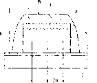
Fig. 3 shows the embodiment (C) of the organic electroluminescent device (bottom emissive type) of single heterojunction structure.It is by the transparent substrate (substrate) 1, transparent anode 2, organic layer 5a (being made of hole transmission layer 6 and electron transfer layer 7) and the negative electrode 3 that are laminated to according to the order of sequence on another.Form with sealing ply 4 sealing ply laminated structures.
Organic electroluminescent device shown in Figure 3 does not have emission layer; It is from the light of launching predetermined wavelength at the interface 20 between hole transmission layer 6 and the electron transfer layer 7.This light is visible by substrate 1.
Fig. 4 shows the embodiment (D) of the organic electroluminescent device (bottom emissive type) of double-heterostructure.It is made up of the transparent substrate 1, transparent anode 2, organic layer 5b (being made of hole transmission layer 10, emission layer 11 and electron transfer layer 12) and the negative electrode 3 that are laminated to according to the order of sequence on another.With sealing ply 4 sealing ply laminated structures.
The mode of operation of organic electroluminescent device shown in Figure 4 is to make the direct current that applies between anode 2 and negative electrode 3 inject electronics by anode 2 injected holes with by negative electrode 3, arrives emission layer 11 thereby make injected holes arrive emission layer 11 by hole transmission layer 10 and make injected electrons pass through electron transfer layer 12 equally.As a result, at emission layer 11 reorganization in electronics and hole takes place, thus the exciton of emission predetermined wavelength light.
At the embodiment of above-mentioned organic electroluminescent device (C) with (D), following material can be used as the hole mobile material with charge transport ability.
The p-diaminodiphenyl of monomer, oligopolymer (oligomer) or polymer form, styrylamine, tritane, porphyrin, triazole, imidazoles, oxadiazole, polyaryl alkane, phenylenediamine, arylamine, oxazole, anthracene, Fluorenone, hydrazone and Stilbene and derivative thereof; The heterocycle conjugated compound, as polysilane-based compound, vinylcarbazole-based compound, thiophene-based compound, and aniline-based compound is (hereinafter suitable equally.)
Their representative instance comprises Alpha-Naphthyl phenylenediamine, porphyrin, metal tetraphenylporphyrin, metal naphthalene cyanines (naphthalocyanine), 4,4 ', 4 " trimethylammonium triphenylamine, 4; 4 '; 4 "-three (3-methyl phenyl phenyl amino) triphenylamine, N, N, N ', N '-four (p-methylphenyl) Ursol D, N, N, N`, N`-tetraphenyl-4, the amino Stilbene of 4`-benzidine, N-phenyl carbazole, 4-di-p-tolyl, poly-(to phenylene vinylidene (paraphenylenevinylene)), poly-(thiophene vinylidene) and gather (2,2 '-thienyl pyrroles).They only exemplify.
In addition, following material can be used as the electron transport material with charge transport ability.Quinoline, perylene, distyryl (bisstyryl) and pyrazine and derivative thereof are (hereinafter suitable equally.)
Their representative instance comprises oxine aluminium (Alq
3), anthracene, naphthalene, phenanthrene, pyrene, bend (chrysene), perylene, divinyl, tonka bean camphor, acridine and Stilbene and derivative thereof.
Under the situation of the embodiment of organic electroluminescent device (C), organic layer 5a is the laminate layers that is made of hole transmission layer 6 and electron transfer layer 7.They one or both of can be the mixture layer that contains above-mentioned compound of styryl come luminous so that make them.Under the situation of the embodiment of organic electroluminescent device (D), organic layer 5b is by hole transmission layer 10, the emission layer 11 of mixture that contains above-mentioned compound of styryl and the laminate layers that electron transfer layer 12 constitutes.Can be in many ways that layer is structurally-modified, so that for example, make hole transmission layer and electron transfer layer one or both of and come luminous.
Can form hole transmission layer by laminated two or more hole mobile materials on another layer, to improve the hole transport performance.
Under the situation of the embodiment of organic electroluminescent device (C), electron transfer layer 7 serves as emission layer; Yet, depend on by the voltage of power supply 8 supplies, can launch at the interface at hole transmission layer 6 or its.And under the situation of the embodiment of organic electroluminescent device (D), emission layer can also be electron transfer layer 12 or hole transmission layer 10 except being the emission layer 11.The required layer structure of improving the light emission performance is that emission layer 11 (containing at least a fluorescent material material) is placed between hole transmission layer and the electron transfer layer.Perhaps, this fluorescent material can mix in hole transmission layer and electron transfer layer one or both of.In the case, layer structure can have extra thin layer (it is that hole blocking layer or exciton generate layer), with control hole transport or electric transmission.
Sealing ply 4 (it serves as sealing membrane) all covers organic electroluminescent device, so that improve electric charge injection efficiency and luminous efficiency.It can be by keeping bubble-tight metal (as aluminium, Jin Hege), its alloy, silicon compound (as silicon oxide and silicon nitride), organic compound etc. to form.
Fig. 5 shows the embodiment (E) of the organic electroluminescent device (top emission structure) of single heterojunction structure.This element is made of the substrate 1, anode 2, organic layer 5c (being made up of hole transmission layer 6 and electron transfer layer 7) and the transparent or semitransparent negative electrode 3 that are laminated to according to the order of sequence on the another kind.With sealing ply 4 sealing ply laminated structures.In the case, from the light of launching predetermined wavelength at the interface 20 between hole transmission layer 6 and the electron transfer layer 7.This light is visible by negative electrode 3 or sealing ply 4.
Fig. 6 shows the embodiment (F) of organic electroluminescent device (top emission structure).It is made of the substrate 1, anode 2, organic layer 5d (being made of hole injection layer 9, hole transmission layer 10, emission layer 11 and electron transfer layer 12) and the transparent or semitransparent negative electrode 3 that are laminated to according to the order of sequence on the another kind.With sealing ply 4 sealing ply laminated structures.As organic electroluminescent device shown in Figure 4, the reorganization in electronics and hole takes place in emission layer 11, thereby produce the exciton of emission predetermined wavelength light.
At the embodiment of organic electroluminescent device (E) with (F), can be by any reflecting material such as Ag, Au, Al, Cr, In or its alloy form substrate 1.Usually can use a kind of substrate to be used for the element of arranging at matrix (laminar structure as illustrated in Figures 5 and 6).And, can on identical substrate, arrange organic electroluminescent device and other element.
As shown in Figure 6, hole injection layer 9 (being made by inorganic or organic compound or organometallic compound) can randomly place between anode 2 and the hole transmission layer 10, so that improve the electric charge injection efficiency.And in Fig. 5, hole injection layer 9 (not shown) can place between anode 2 and the hole transmission layer 6.Incidentally, forming under the situation of sealing ply 4, can on the horizontal plane of anode 2, form insulation layer and be used for insulation by electro-conductive material (as metal).
In the embodiment of organic electroluminescent device (E), organic layer 5c is the lamination organic layer that is made of hole transmission layer 6 and electron transfer layer 7.Hole transmission layer 6 and electron transfer layer 7 one or both of can be the mixture layers that contains above-mentioned compound of styryl, come luminous so that make them.In the embodiment of organic electroluminescent device (F), organic layer 5d is by hole transmission layer 10, the emission layer 11 of mixture that contains above-mentioned compound of styryl and the lamination organic layer that electron transfer layer 12 constitutes.Can be in many ways that layer is structurally-modified, so that for example, make hole transmission layer and electron transfer layer one or both of and come luminous.
Can form hole transmission layer by laminated two or more hole mobile materials on another layer, to improve the hole transport performance.
In the embodiment of organic electroluminescent device (E), electron transfer layer 7 serves as emission layer; Yet, depend on by the voltage of power supply 8 supplies, can launch at the interface at hole transmission layer 6 or its.And under the situation of the embodiment of organic electroluminescent device (F), emission layer can also be electron transfer layer 12 or hole transmission layer 10 except being the emission layer 11.The required layer structure of improving the light emission performance makes emission layer 11 (containing at least a fluorescent material material) place between hole transmission layer and the electron transfer layer.Perhaps, this fluorescent material can mix in hole transmission layer and electron transfer layer one or both of.In the case, layer structure can have extra thin layer (it is that hole blocking layer or exciton generate layer), with control hole transport or electric transmission.
Sealing ply 4 (it serves as sealing membrane) all covers organic electroluminescent device, so that improve electric charge injection efficiency and luminous efficiency.It can be by keeping bubble-tight metal (as aluminium, Jin Hege), its alloy, silicon compound (as silicon oxide and silicon nitride) etc. to form.
At the embodiment of organic electroluminescent device (E) with (F), emission layer is fixed between anode and the negative electrode, and therefore, the light of being launched is disturbed by multi-beam between anode and negative electrode.If anode and negative electrode have suitably the optical property of (adequate) (as reflectivity and transmissivity) and between them the fixed organic layer have suitable thickness, might pro utilize the multi-beam effects of jamming.Therefore, might control from organic electroluminescent device (E) or the light wavelength of sending (F).In such a way, might improve the colourity of the light of being launched.Incidentally, J.Yamada etc. are at AM-LCDDigest of Technical Papers, and OD-2 has mentioned multi-beam interferential mechanism in the 77-80 page or leaf (2002).
Usually drive above-mentioned organic electroluminescent device by applying direct current.Yet, also can use pulsed current or alternating-current.Any ampere and voltage number are admissible, remove NOT element and are broken up.Yet in view of the life-span of watt consumption and organic electroluminescent device, the effective light emission with minimum electric energy is required.
Fig. 7 is the synoptic diagram that shows the flat panel display configuration with organic electroluminescent device of the present invention.As shown in the figure, for example, panchromatic flat-panel monitor is made of anode 2 and negative electrode 3 and the organic layer 5 that is fixed between them.Organic layer 5 is to launch three kinds of main colors, any organic layer 5a, 5b, 5c and the 5d of red (R), green (G) and blue (B).Anode 2 and negative electrode 3 are cross one another fillets.Select them by luminance signal circuit 14 and the pilot circuit 15 that contains stepping register, so that the electrode of selecting provides signal voltage.Therefore, organic layer is gone up the emission bright dipping in the position (or pixel) of anode of selecting 2 and negative electrode 3 intersections.
Flat-panel monitor shown in Figure 7 belongs to simple matrix type (8 * 3RGB).Its structure makes organic layer 5 be fixed between anode 2 and the negative electrode 3, and described organic layer 5 is any at least of hole transmission layer, emission layer and electron transfer layer.(with reference to figure 3 or 4, and Fig. 5 or 6) composition anode and negative electrode in fillet, wherein the former intersects with the right angle and the latter, forms matrix.They receive according to the order of sequence from luminance signal circuit 14 and the signal voltage that contains the pilot circuit 15 of stepping register, so that luminous at the intersection point place.Gou Zao EL element not only can be used as letter and code indicating meter as mentioned above, and can be used as the reproduction of image device.A kind of replacement scheme is the polychrome or the panchromatic flat-panel monitor of all solids (solid) type, and wherein anode in bar paten 2 and negative electrode 3 are given redness (R), green (G) and blue (B) separately.EL element can drive and the active-matrix driving by simple matrix.
Now, describe the present invention, wherein do not plan to limit its scope with described embodiment with reference to following embodiment.
This embodiment has illustrated the organic electroluminescent device (bottom emissive type) of single heterojunction structure, wherein amino-benzene vinyl compound (it is one of compound of styryl of the above general formula that provides [I] expression) and the mixture of α-NPD (Alpha-Naphthyl phenylenediamine) by following structural formula (17)-11 expression forms hole transmission layer, and described hole transmission layer also serves as emission layer (hole transport and emission layer).
At first, (size is 30mm * 30mm) to place glass substrate in vacuum deposition apparatus.This glass substrate has the ITO film anode (100nm is thick) that forms on one surface.Glass substrate is 10
-4Pa or lower experience vacuum moulding machine, it has the metal mask (mask) near its arrangement, and described metal mask has a plurality of openings, and size is 2.0mm * 2.0mm separately.Vacuum moulding machine produces the thick hole transmission layer (it also serves as emission layer) of 50nm, and described hole transmission layer is made of as the weight ratio of hole mobile material with 1: 1 compound of styryl and the α-NPD of the above structural formula that provides (17)-11 expression.For each component, the adjusting sedimentation velocity is 0.1nm/s.
Then, by vacuum moulding machine, the Alq that represents by following structural formula
3(three (oxine) aluminium) forms the thick electron transfer layer of 50nm on hole transmission layer.The adjusting sedimentation velocity is 0.2nm/s.

By vacuum moulding machine, form the thick negative electrode of 200nm by the Mg and the Ag of 1: 3 ratio of mixture.In such a way, obtain the organic electroluminescent device of embodiment 1 shown in Figure 3.
Under nitrogen atmosphere, by applying forward bias direct current (forwardd bias direct current), the luminescence feature of the organic electroluminescent device of the embodiment 1 that test so obtains.Its red-emitting finds that by spectrometry it has the peak value of about 620nm.Be furnished with the spectroscope (by Otsuka Electronics Co., Ltd. make) of photodiode array detector by use, carry out spectrometry.It produces 1500cd/m under 8V
2Brightness.
After leaving standstill 1 month in nitrogen atmosphere, sample does not demonstrate the sign of degraded (degradeation).Accelerated degradation test (in this test, keeps producing 300cd/m
2The electric current of initial brightness) shows the brightness needs cost 2500 hours that reduces by half.
This embodiment has illustrated the organic electroluminescent device (bottom emissive type) of single heterojunction structure, wherein by the compound of styryl (it is one of compound of styryl of the above general formula that provides [I] expression) of the above structural formula that provides (17)-11 expression and more than the Alq that represents of the structural formula that provides
3Mixture form electron transfer layer, described electron transfer layer also serves as emission layer (electric transmission and emission layer).
At first, (size is 30mm * 30mm) to place glass substrate in vacuum deposition apparatus.This glass substrate has the ITO film anode (100nm is thick) that forms on one surface.Glass substrate is 10
-4Pa or lower experience vacuum moulding machine, it has the metal mask near its arrangement, and described metal mask has a plurality of openings, and size is 2.0mm * 2.0mm separately.α-NPD layer that the structural formula that provides more than vacuum moulding machine generation 50nm is thick is represented.The adjusting sedimentation velocity is 0.1nm/s.
Then, by vacuum moulding machine, by the amino-benzene vinyl compound and the Alq of the above structural formula that provides (17)-11 expression
3Mixture as the weight blending ratio of electron transport material with 1: 1, on hole transmission layer, form thick electric transmission and the emission layer of 50nm.For each component, the adjusting sedimentation velocity is 0.2nm/s.
By vacuum moulding machine, form the thick negative electrode of 200nm by the Mg and the Ag of 1: 3 ratio of mixture.In such a way, obtain the organic electroluminescent device of embodiment 2 shown in Figure 3.
Under nitrogen atmosphere, by applying the forward bias direct current, the luminescence feature of the organic electroluminescent device that test so obtains.Its red-emitting finds that by spectrometry (as embodiment 1) it has the peak value of about 620nm.It produces 2600cd/m under 8V
2Brightness.
After leaving standstill 1 month in nitrogen atmosphere, sample does not demonstrate the sign of degraded.Accelerated degradation test (in this test, keeps producing 300cd/m
2The electric current of initial brightness) shows the brightness needs cost 2700 hours that reduces by half.
This embodiment has illustrated the organic electroluminescent device (bottom emissive type) of double-heterostructure, wherein by the compound of styryl (it is one of compound of styryl of the above general formula that provides [I] expression) of the above structural formula that provides (17)-11 expression and more than the Alq that represents of the structural formula that provides
3Mixture form electric transmission and emission layer.
At first, (size is 30mm * 30mm) to place glass substrate in vacuum deposition apparatus.This glass substrate has the ITO film anode (100nm is thick) that forms on one surface.Glass substrate is 10
-4Pa or lower experience vacuum moulding machine, it has the metal mask near its arrangement, and described metal mask has a plurality of openings, and size is 2.0mm * 2.0mm separately.α-NPD layer that the structural formula that provides more than vacuum moulding machine generation 30nm is thick is represented.The adjusting sedimentation velocity is 0.2nm/s.
Then, deposit emissive material on hole transmission layer, described emissive material is the compound of styryl and the Alq of the above structural formula that provides (17)-11 expression
3Mixture with 1: 1 weight blending ratio formation.Thereby form compound of styryl and Alq by the above structural formula that provides (17)-11 expression
3The thick emission layer of 30nm that constitutes.For each component, the adjusting sedimentation velocity is 0.2nm/s.
The Alq that the structural formula that provides more than the use is represented
3As electron transport material, on emission layer, carry out vacuum moulding machine.Form the thick Alq of 30nm
3Film.The adjusting sedimentation velocity is 0.2nm/s.
By vacuum moulding machine, form the thick negative electrode of 200nm by the Mg and the Ag of 1: 3 ratio of mixture.In such a way, obtain the organic electroluminescent device of embodiment 3 shown in Figure 4.
Under nitrogen atmosphere, by applying the forward bias direct current, the luminescence feature of the organic electroluminescent device that test so obtains.Its red-emitting finds that by spectrometry (as embodiment 1) it has the peak value of about 620nm.It produces 3200cd/m under 8V
2Brightness.
After leaving standstill 1 month in nitrogen atmosphere, sample does not demonstrate the sign of degraded.Accelerated degradation test (in this test, keeps producing 300cd/m
2The electric current of initial brightness) shows the brightness needs cost 3500 hours that reduces by half.
This embodiment has illustrated the organic electroluminescent device (bottom emissive type) of double-heterostructure, wherein the mixture by the compound of styryl of the compound of styryl of the above structural formula that provides (17)-11 expression and the following structural formula that provides (17)-1 expression forms emission layer, and wherein these two kinds of compound of styryl are the members in the compound of styryl represented of the above general formula that provides [I].
(17)-1:

At first, (size is 30mm * 30mm) to place glass substrate in vacuum deposition apparatus.This glass substrate has the ITO film anode (100nm is thick) that forms on one surface.Glass substrate is 10
-4Pa or lower experience vacuum moulding machine, it has the metal mask near its arrangement, and described metal mask has a plurality of openings, and size is 2.0mm * 2.0mm separately.α-NPD layer that the structural formula that provides more than vacuum moulding machine generation 30nm is thick is represented.The adjusting sedimentation velocity is 0.2nm/s.
Then, codeposition emissive material on hole transmission layer, described emissive material are the mixtures that the compound of styryl of the compound of styryl of the above structural formula that provides (17)-11 expression and the above structural formula that provides (17)-1 expression constitutes with 1: 3 weight blending ratio.So form the thick emission layer of 30nm of the compound of styryl formation of representing by the compound of styryl and the above structural formula that provides (17)-1 of the above structural formula that provides (17)-11 expression.For first kind of component, the adjusting sedimentation velocity is 0.1nm/s, and for second kind of component, the adjusting sedimentation velocity is 0.3nm/s.
The Alq that the structural formula that provides more than the use is represented
3As electron transport material, on emission layer, carry out vacuum moulding machine.Form the thick Alq of 30nm
3Film.The adjusting sedimentation velocity is 0.2nm/s.
By vacuum moulding machine, form the thick negative electrode of 200nm by the Mg and the Ag of 1: 3 ratio of mixture.In such a way, obtain the organic electroluminescent device of embodiment 4 shown in Figure 4.
Under nitrogen atmosphere, by applying the forward bias direct current, the luminescence feature of the organic electroluminescent device of the embodiment 4 that test so obtains.It launches bisque light, finds that by spectrometry (as embodiment 1) it has peak value at the 610nm place.It produces 2200cd/m under 8V
2Brightness.
After leaving standstill 1 month in nitrogen atmosphere, sample does not demonstrate the sign of degraded.Accelerated degradation test (in this test, keeps producing 300cd/m
2The electric current of initial brightness) shows the brightness needs cost 1000 hours that reduces by half.
This embodiment has illustrated the organic electroluminescent device (bottom emissive type) of single heterojunction structure, wherein by the compound of styryl (it is one of compound of styryl of the above general formula that provides [I] expression) of the above structural formula that provides (17)-1 expression and more than the Alq that represents of the structural formula that provides
3Mixture form electric transmission and emission layer.
This organic electroluminescent device is consistent with layer structure and film formation method that embodiment 2 mentions.
Under nitrogen atmosphere, by applying the forward bias direct current, the luminescence feature of the organic electroluminescent device of the embodiment 5 that test so obtains.It launches bisque light, finds that by spectrometry (as embodiment 1) it has peak value at about 608nm place.It produces 1000cd/m under 8V
2Brightness.
After leaving standstill 1 month in nitrogen atmosphere, sample does not demonstrate the sign of degraded.Accelerated degradation test (in this test, keeps producing 300cd/m
2The electric current of initial brightness) shows the brightness needs cost 800 hours that reduces by half.
Embodiment 6
This embodiment has illustrated the organic electroluminescent device (bottom emissive type) of single heterojunction structure, wherein by the compound of styryl (it is one of compound of styryl of the above general formula that provides [I] expression) of following structural formula (17)-2 expression and more than the Alq that represents of the structural formula that provides
3Mixture form electric transmission and emission layer.
This organic electroluminescent device is consistent with layer structure and film formation method that embodiment 2 mentions.
Under nitrogen atmosphere, by applying the forward bias direct current, the luminescence feature of the organic electroluminescent device of the embodiment 6 that test so obtains.It launches bisque light, finds that by spectrometry (as embodiment 1) it has peak value at about 610nm place.It produces 500cd/m under 8V
2Brightness.
After leaving standstill 1 month in nitrogen atmosphere, sample does not demonstrate the sign of degraded.Accelerated degradation test (in this test, keeps producing 300cd/m
2The electric current of initial brightness) shows the brightness needs cost 700 hours that reduces by half.
This embodiment has illustrated the organic electroluminescent device (bottom emissive type) of single heterojunction structure, wherein by the compound of styryl (it is one of compound of styryl of the above general formula that provides [I] expression) of following structural formula (17)-3 expression and more than the Alq that represents of the structural formula that provides
3Mixture form electric transmission and emission layer.
This organic electroluminescent device is consistent with layer structure and film formation method that embodiment 2 mentions.
Under nitrogen atmosphere, by applying the forward bias direct current, the luminescence feature of the organic electroluminescent device of the embodiment 7 that test so obtains.It launches bisque light, finds that by spectrometry (as embodiment 1) it has peak value at about 605nm place.It produces 1200cd/m under 8V
2Brightness.
After leaving standstill 1 month in nitrogen atmosphere, sample does not demonstrate the sign of degraded.Accelerated degradation test (in this test, keeps producing 300cd/m
2The electric current of initial brightness) shows the brightness needs cost 1100 hours that reduces by half.
Embodiment 8
This embodiment has illustrated the organic electroluminescent device (bottom emissive type) of single heterojunction structure, wherein by the compound of styryl (it is one of compound of styryl of the above general formula that provides [I] expression) of following structural formula (17)-4 expression and more than the Alq that represents of the structural formula that provides
3Mixture form electric transmission and emission layer.

This organic electroluminescent device is consistent with layer structure and film formation method that embodiment 2 mentions.
Under nitrogen atmosphere, by applying the forward bias direct current, the luminescence feature of the organic electroluminescent device of the embodiment 8 that test so obtains.It launches bisque light, finds that by spectrometry (as embodiment 1) it has peak value at about 600nm place.It produces 1000cd/m under 8V
2Brightness.
After leaving standstill 1 month in nitrogen atmosphere, sample does not demonstrate the sign of degraded.Accelerated degradation test (in this test, keeps producing 300cd/m
2The electric current of initial brightness) shows the brightness needs cost 1400 hours that reduces by half.
This embodiment has illustrated the organic electroluminescent device (bottom emissive type) of single heterojunction structure, wherein by the compound of styryl (it is one of compound of styryl of the above general formula that provides [I] expression) of following structural formula (17)-5 expression and more than the Alq that represents of the structural formula that provides
3Mixture form electric transmission and emission layer.

This organic electroluminescent device is consistent with layer structure and film formation method that embodiment 2 mentions.
Under nitrogen atmosphere, by applying the forward bias direct current, the luminescence feature of the organic electroluminescent device of the embodiment 9 that test so obtains.It launches bisque light, finds that by spectrometry (as embodiment 1) it has peak value at about 615nm place.It produces 900cd/m under 8V
2Brightness.
After leaving standstill 1 month in nitrogen atmosphere, sample does not demonstrate the sign of degraded.Accelerated degradation test (in this test, keeps producing 300cd/m
2The electric current of initial brightness) shows the brightness needs cost 850 hours that reduces by half.
This embodiment has illustrated the organic electroluminescent device (bottom emissive type) of single heterojunction structure, wherein by the compound of styryl (it is one of compound of styryl of the above general formula that provides [I] expression) of following structural formula (17)-6 expression and more than the Alq that represents of the structural formula that provides
3Mixture form electric transmission and emission layer.
This organic electroluminescent device is consistent with layer structure and film formation method that embodiment 2 mentions.
Under nitrogen atmosphere, by applying the forward bias direct current, the luminescence feature of the organic electroluminescent device of the embodiment 10 that test so obtains.Its red-emitting finds that by spectrometry (as embodiment 1) it has peak value at about 620nm place.It produces 800cd/m under 8V
2Brightness.
After leaving standstill 1 month in nitrogen atmosphere, sample does not demonstrate the sign of degraded.Accelerated degradation test (in this test, keeps producing 300cd/m
2The electric current of initial brightness) shows the brightness needs cost 700 hours that reduces by half.
This embodiment has illustrated the organic electroluminescent device (bottom emissive type) of single heterojunction structure, wherein by the compound of styryl (it is one of compound of styryl of the above general formula that provides [I] expression) of following structural formula (17)-7 expression and more than the Alq that represents of the structural formula that provides
3Mixture form electric transmission and emission layer.
This organic electroluminescent device is consistent with layer structure and film formation method that embodiment 2 mentions.
Under nitrogen atmosphere, by applying the forward bias direct current, the luminescence feature of the organic electroluminescent device of the embodiment 11 that test so obtains.It launches bisque light, finds that by spectrometry (as embodiment 1) it has peak value at about 615nm place.It produces 1100cd/m under 8V
2Brightness.
After leaving standstill 1 month in nitrogen atmosphere, sample does not demonstrate the sign of degraded.Accelerated degradation test (in this test, keeps producing 300cd/m
2The electric current of initial brightness) shows the brightness needs cost 1000 hours that reduces by half.
This embodiment has illustrated the organic electroluminescent device (bottom emissive type) of single heterojunction structure, wherein by the compound of styryl (it is one of compound of styryl of the above general formula that provides [I] expression) of following structural formula (17)-8 expression and more than the Alq that represents of the structural formula that provides
3Mixture form electric transmission and emission layer.
This organic electroluminescent device is consistent with layer structure and film formation method that embodiment 2 mentions.
Under nitrogen atmosphere, by applying the forward bias direct current, the luminescence feature of the organic electroluminescent device of the embodiment 12 that test so obtains.It launches bisque light, finds that by spectrometry (as embodiment 1) it has peak value at about 610nm place.It produces 950cd/m under 8V
2Brightness.
After leaving standstill 1 month in nitrogen atmosphere, sample does not demonstrate the sign of degraded.Accelerated degradation test (in this test, keeps producing 300cd/m
2The electric current of initial brightness) shows the brightness needs cost 1300 hours that reduces by half.
Embodiment 13
This embodiment has illustrated the organic electroluminescent device (bottom emissive type) of single heterojunction structure, wherein by the compound of styryl (it is one of compound of styryl of the above general formula that provides [I] expression) of following structural formula (17)-9 expression and more than the Alq that represents of the structural formula that provides
3Mixture form electric transmission and emission layer.
This organic electroluminescent device is consistent with layer structure and film formation method that embodiment 2 mentions.
Under nitrogen atmosphere, by applying the forward bias direct current, the luminescence feature of the organic electroluminescent device of the embodiment 13 that test so obtains.It launches bisque light, finds that by spectrometry (as embodiment 1) it has peak value at about 605nm place.It produces 850cd/m under 8V
2Brightness.
After leaving standstill 1 month in nitrogen atmosphere, sample does not demonstrate the sign of degraded.Accelerated degradation test (in this test, keeps producing 300cd/m
2The electric current of initial brightness) shows the brightness needs cost 650 hours that reduces by half.
Embodiment 14
This embodiment has illustrated the organic electroluminescent device (bottom emissive type) of single heterojunction structure, wherein by the compound of styryl (it is one of compound of styryl of the above general formula that provides [I] expression) of following structural formula (17)-10 expression and more than the Alq that represents of the structural formula that provides
3Mixture form electric transmission and emission layer.

This organic electroluminescent device is consistent with layer structure and film formation method that embodiment 2 mentions.
Under nitrogen atmosphere, by applying the forward bias direct current, the luminescence feature of the organic electroluminescent device of the embodiment 14 that test so obtains.It launches bisque light, finds that by spectrometry (as embodiment 1) it has peak value at about 610nm place.It produces 750cd/m under 8V
2Brightness.
After leaving standstill 1 month in nitrogen atmosphere, sample does not demonstrate the sign of degraded.Accelerated degradation test (in this test, keeps producing 300cd/m
2The electric current of initial brightness) shows the brightness needs cost 500 hours that reduces by half.
Embodiment 15
This embodiment has illustrated the organic electroluminescent device (bottom emissive type) of single heterojunction structure, wherein by the compound of styryl (it is one of compound of styryl of the above general formula that provides [I] expression) of following structural formula (17)-12 expression and more than the Alq that represents of the structural formula that provides
3Mixture form electric transmission and emission layer.
This organic electroluminescent device is consistent with layer structure and film formation method that embodiment 2 mentions.
Under nitrogen atmosphere, by applying the forward bias direct current, the luminescence feature of the organic electroluminescent device of the embodiment 15 that test so obtains.Its red-emitting finds that by spectrometry (as embodiment 1) it has peak value at about 625nm place.It produces 1000cd/m under 8V
2Brightness.
After leaving standstill 1 month in nitrogen atmosphere, sample does not demonstrate the sign of degraded.Accelerated degradation test (in this test, keeps producing 300cd/m
2The electric current of initial brightness) shows the brightness needs cost 1500 hours that reduces by half.
Embodiment 16
This embodiment has illustrated the organic electroluminescent device (bottom emissive type) of single heterojunction structure, wherein by the compound of styryl (it is one of compound of styryl of the above general formula that provides [I] expression) of following structural formula (17)-13 expression and more than the Alq that represents of the structural formula that provides
3Mixture form electric transmission and emission layer.
This organic electroluminescent device is consistent with layer structure and film formation method that embodiment 2 mentions.
Under nitrogen atmosphere, by applying the forward bias direct current, the luminescence feature of the organic electroluminescent device of the embodiment 16 that test so obtains.It launches bisque light, finds that by spectrometry (as embodiment 1) it has peak value at about 610nm place.It produces 2000cd/m under 8V
2Brightness.
After leaving standstill 1 month in nitrogen atmosphere, sample does not demonstrate the sign of degraded.Accelerated degradation test (in this test, keeps producing 300cd/m
2The electric current of initial brightness) shows the brightness needs cost 2800 hours that reduces by half.
Embodiment 17
This embodiment has illustrated the organic electroluminescent device (bottom emissive type) of single heterojunction structure, wherein by the compound of styryl (it is one of compound of styryl of the above general formula that provides [I] expression) of following structural formula (17)-14 expression and more than the Alq that represents of the structural formula that provides
3Mixture form electric transmission and emission layer.
This organic electroluminescent device is consistent with layer structure and film formation method that embodiment 2 mentions.
Under nitrogen atmosphere, by applying the forward bias direct current, the luminescence feature of the organic electroluminescent device of the embodiment 17 that test so obtains.It launches bisque light, finds that by spectrometry (as embodiment 1) it has peak value at about 605nm place.It produces 1800cd/m under 8V
2Brightness.
After leaving standstill 1 month in nitrogen atmosphere, sample does not demonstrate the sign of degraded.Accelerated degradation test (in this test, keeps producing 300cd/m
2The electric current of initial brightness) shows the brightness needs cost 3300 hours that reduces by half.
Embodiment 18
This embodiment has illustrated the organic electroluminescent device (bottom emissive type) of single heterojunction structure, wherein by the compound of styryl (it is one of compound of styryl of the above general formula that provides [I] expression) of following structural formula (17)-15 expression and more than the Alq that represents of the structural formula that provides
3Mixture form electric transmission and emission layer.
This organic electroluminescent device is consistent with layer structure and film formation method that embodiment 2 mentions.
Under nitrogen atmosphere, by applying the forward bias direct current, the luminescence feature of the organic electroluminescent device of the embodiment 18 that test so obtains.It launches bisque light, finds that by spectrometry (as embodiment 1) it has peak value at about 605nm place.It produces 880cd/m under 8V
2Brightness.
After leaving standstill 1 month in nitrogen atmosphere, sample does not demonstrate the sign of degraded.Accelerated degradation test (in this test, keeps producing 300cd/m
2The electric current of initial brightness) shows the brightness needs cost 700 hours that reduces by half.
Embodiment 19
This embodiment has illustrated the organic electroluminescent device (bottom emissive type) of single heterojunction structure, wherein by the compound of styryl (it is one of compound of styryl of the above general formula that provides [I] expression) of following structural formula (17)-16 expression and more than the Alq that represents of the structural formula that provides
3Mixture form electric transmission and emission layer.
This organic electroluminescent device is consistent with layer structure and film formation method that embodiment 2 mentions.
Under nitrogen atmosphere, by applying the forward bias direct current, the luminescence feature of the organic electroluminescent device of the embodiment 19 that test so obtains.It launches bisque light, finds that by spectrometry (as embodiment 1) it has peak value at about 605nm place.It produces 900cd/m under 8V
2Brightness.
After leaving standstill 1 month in nitrogen atmosphere, sample does not demonstrate the sign of degraded.Accelerated degradation test (in this test, keeps producing 300cd/m
2The electric current of initial brightness) shows the brightness needs cost 850 hours that reduces by half.
This embodiment has illustrated the organic electroluminescent device (bottom emissive type) of single heterojunction structure, wherein by the compound of styryl (it is one of compound of styryl of the above general formula that provides [I] expression) of following structural formula (17)-17 expression and more than the Alq that represents of the structural formula that provides
3Mixture form electric transmission and emission layer.
This organic electroluminescent device is consistent with layer structure and film formation method that embodiment 2 mentions.
Under nitrogen atmosphere, by applying the forward bias direct current, the luminescence feature of the organic electroluminescent device of the embodiment 20 that test so obtains.Its red-emitting finds that by spectrometry (as embodiment 1) it has peak value at about 700nm place.It produces 250cd/m under 8V
2Brightness.
After leaving standstill 1 month in nitrogen atmosphere, sample does not demonstrate the sign of degraded.Accelerated degradation test (in this test, keeps producing 300cd/m
2The electric current of initial brightness) shows the brightness needs cost 350 hours that reduces by half.
Embodiment 21
This embodiment has illustrated the organic electroluminescent device (bottom emissive type) of single heterojunction structure, wherein by the compound of styryl (it is one of compound of styryl of the above general formula that provides [I] expression) of following structural formula (17)-18 expression and more than the Alq that represents of the structural formula that provides
3Mixture form electric transmission and emission layer.

This organic electroluminescent device is consistent with layer structure and film formation method that embodiment 2 mentions.
Under nitrogen atmosphere, by applying the forward bias direct current, the luminescence feature of the organic electroluminescent device of the embodiment 21 that test so obtains.Its red-emitting finds that by spectrometry (as embodiment 1) it has peak value at about 690nm place.It produces 180cd/m under 8V
2Brightness.
After leaving standstill 1 month in nitrogen atmosphere, sample does not demonstrate the sign of degraded.Accelerated degradation test (in this test, keeps producing 300cd/m
2The electric current of initial brightness) shows the brightness needs cost 450 hours that reduces by half.
Embodiment 22
This embodiment has illustrated the organic electroluminescent device (bottom emissive type) of single heterojunction structure, wherein by the compound of styryl (it is one of compound of styryl of the above general formula that provides [I] expression) of following structural formula (17)-19 expression and more than the Alq that represents of the structural formula that provides
3Mixture form electric transmission and emission layer.
This organic electroluminescent device is consistent with layer structure and film formation method that embodiment 2 mentions.
Under nitrogen atmosphere, by applying the forward bias direct current, the luminescence feature of the organic electroluminescent device of the embodiment 22 that test so obtains.Its red-emitting finds that by spectrometry (as embodiment 1) it has peak value at about 690nm place.It produces 330cd/m under 8V
2Brightness.
After leaving standstill 1 month in nitrogen atmosphere, sample does not demonstrate the sign of degraded.Accelerated degradation test (in this test, keeps producing 300cd/m
2The electric current of initial brightness) shows the brightness needs cost 390 hours that reduces by half.
Embodiment 23
This embodiment has illustrated the organic electroluminescent device (bottom emissive type) of single heterojunction structure, wherein by the compound of styryl (it is one of compound of styryl of the above general formula that provides [I] expression) of following structural formula (17)-20 expression and more than the Alq that represents of the structural formula that provides
3Mixture form electric transmission and emission layer.
This organic electroluminescent device is consistent with layer structure and film formation method that embodiment 2 mentions.
Under nitrogen atmosphere, by applying the forward bias direct current, the luminescence feature of the organic electroluminescent device of the embodiment 23 that test so obtains.Its red-emitting finds that by spectrometry (as embodiment 1) it has peak value at about 680nm place.It produces 280cd/m under 8V
2Brightness.
After leaving standstill 1 month in nitrogen atmosphere, sample does not demonstrate the sign of degraded.Accelerated degradation test (in this test, keeps producing 300cd/m
2The electric current of initial brightness) shows the brightness needs cost 500 hours that reduces by half.
Embodiment 24
This embodiment has illustrated the organic electroluminescent device (bottom emissive type) of single heterojunction structure, wherein by the compound of styryl (it is one of compound of styryl of the above general formula that provides [I] expression) of following structural formula (17)-21 expression and more than the Alq that represents of the structural formula that provides
3Mixture form electric transmission and emission layer.

This organic electroluminescent device is consistent with layer structure and film formation method that embodiment 2 mentions.
Under nitrogen atmosphere, by applying the forward bias direct current, the luminescence feature of the organic electroluminescent device of the embodiment 24 that test so obtains.Its red-emitting finds that by spectrometry (as embodiment 1) it has peak value at about 680nm place.It produces 220cd/m under 8V
2Brightness.
After leaving standstill 1 month in nitrogen atmosphere, sample does not demonstrate the sign of degraded.Accelerated degradation test (in this test, keeps producing 300cd/m
2The electric current of initial brightness) shows the brightness needs cost 210 hours that reduces by half.
Embodiment 25
This embodiment has illustrated the organic electroluminescent device (bottom emissive type) of single heterojunction structure, wherein by the compound of styryl (it is one of compound of styryl of the above general formula that provides [I] expression) of following structural formula (17)-22 expression and more than the Alq that represents of the structural formula that provides
3Mixture form electric transmission and emission layer.

This organic electroluminescent device is consistent with layer structure and film formation method that embodiment 2 mentions.
Under nitrogen atmosphere, by applying the forward bias direct current, the luminescence feature of the organic electroluminescent device of the embodiment 25 that test so obtains.Its red-emitting finds that by spectrometry (as embodiment 1) it has peak value at about 675nm place.It produces 240cd/m under 8V
2Brightness.
After leaving standstill 1 month in nitrogen atmosphere, sample does not demonstrate the sign of degraded.Accelerated degradation test (in this test, keeps producing 300cd/m
2The electric current of initial brightness) shows the brightness needs cost 240 hours that reduces by half.
Embodiment 26
This embodiment has illustrated the organic electroluminescent device (bottom emissive type) of single heterojunction structure, wherein by the compound of styryl (it is one of compound of styryl of the above general formula that provides [I] expression) of following structural formula (17)-23 expression and more than the Alq that represents of the structural formula that provides
3Mixture form electric transmission and emission layer.

This organic electroluminescent device is consistent with layer structure and film formation method that embodiment 2 mentions.
Under nitrogen atmosphere, by applying the forward bias direct current, the luminescence feature of the organic electroluminescent device of the embodiment 26 that test so obtains.Its red-emitting finds that by spectrometry (as embodiment 1) it has peak value at about 680nm place.It produces 260cd/m under 8V
2Brightness.
After leaving standstill 1 month in nitrogen atmosphere, sample does not demonstrate the sign of degraded.Accelerated degradation test (in this test, keeps producing 300cd/m
2The electric current of initial brightness) shows the brightness needs cost 320 hours that reduces by half.
Embodiment 27
This embodiment has illustrated the organic electroluminescent device (bottom emissive type) of single heterojunction structure, wherein by the compound of styryl (it is one of compound of styryl of the above general formula that provides [I] expression) of following structural formula (17)-24 expression and more than the Alq that represents of the structural formula that provides
3Mixture form electric transmission and emission layer.
This organic electroluminescent device is consistent with layer structure and film formation method that embodiment 2 mentions.
Under nitrogen atmosphere, by applying the forward bias direct current, the luminescence feature of the organic electroluminescent device of the embodiment 27 that test so obtains.Its red-emitting finds that by spectrometry (as embodiment 1) it has peak value at about 680nm place.It produces 180cd/m under 8V
2Brightness.
After leaving standstill 1 month in nitrogen atmosphere, sample does not demonstrate the sign of degraded.Accelerated degradation test (in this test, keeps producing 300cd/m
2The electric current of initial brightness) shows the brightness needs cost 280 hours that reduces by half.
Embodiment 28
This embodiment has illustrated the organic electroluminescent device (bottom emissive type) of single heterojunction structure, wherein by the compound of styryl (it is one of compound of styryl of the above general formula that provides [I] expression) of following structural formula (17)-25 expression and more than the Alq that represents of the structural formula that provides
3Mixture form electric transmission and emission layer.
This organic electroluminescent device is consistent with layer structure and film formation method that embodiment 2 mentions.
Under nitrogen atmosphere, by applying the forward bias direct current, the luminescence feature of the organic electroluminescent device of the embodiment 28 that test so obtains.Its red-emitting finds that by spectrometry (as embodiment 1) it has peak value at about 675nm place.It produces 340cd/m under 8V
2Brightness.
After leaving standstill 1 month in nitrogen atmosphere, sample does not demonstrate the sign of degraded.Accelerated degradation test (in this test, keeps producing 300cd/m
2The electric current of initial brightness) shows the brightness needs cost 600 hours that reduces by half.
Embodiment 29
This embodiment has illustrated the organic electroluminescent device (bottom emissive type) of single heterojunction structure, wherein by the compound of styryl (it is one of compound of styryl of the above general formula that provides [I] expression) of following structural formula (1 7)-26 expression and more than the Alq that represents of the structural formula that provides
3Mixture form electric transmission and emission layer.
This organic electroluminescent device is consistent with layer structure and film formation method that embodiment 2 mentions.
Under nitrogen atmosphere, by applying the forward bias direct current, the luminescence feature of the organic electroluminescent device of the embodiment 29 that test so obtains.Its red-emitting finds that by spectrometry (as embodiment 1) it has peak value at about 630nm place.It produces 550cd/m under 8V
2Brightness.
After leaving standstill 1 month in nitrogen atmosphere, sample does not demonstrate the sign of degraded.Accelerated degradation test (in this test, keeps producing 300cd/m
2The electric current of initial brightness) shows the brightness needs cost 780 hours that reduces by half.
Embodiment 30
This embodiment has illustrated the organic electroluminescent device (bottom emissive type) of single heterojunction structure, wherein by the compound of styryl (it is one of compound of styryl of the above general formula that provides [I] expression) of following structural formula (17)-27 expression and more than the Alq that represents of the structural formula that provides
3Mixture form electric transmission and emission layer.
This organic electroluminescent device is consistent with layer structure and film formation method that embodiment 2 mentions.
Under nitrogen atmosphere, by applying the forward bias direct current, the luminescence feature of the organic electroluminescent device of the embodiment 30 that test so obtains.Its red-emitting finds that by spectrometry (as embodiment 1) it has peak value at about 640nm place.It produces 700cd/m under 8V
2Brightness.
After leaving standstill 1 month in nitrogen atmosphere, sample does not demonstrate the sign of degraded.Accelerated degradation test (in this test, keeps producing 300cd/m
2The electric current of initial brightness) shows the brightness needs cost 1500 hours that reduces by half.
Embodiment 31
This embodiment has illustrated the organic electroluminescent device (bottom emissive type) of single heterojunction structure, wherein by the compound of styryl (it is one of compound of styryl of the above general formula that provides [I] expression) of following structural formula (17)-28 expression and more than the Alq that represents of the structural formula that provides
3Mixture form electric transmission and emission layer.
This organic electroluminescent device is consistent with layer structure and film formation method that embodiment 2 mentions.
Under nitrogen atmosphere, by applying the forward bias direct current, the luminescence feature of the organic electroluminescent device of the embodiment 31 that test so obtains.Its red-emitting finds that by spectrometry (as embodiment 1) it has peak value at about 645nm place.It produces 720cd/m under 8V
2Brightness.
After leaving standstill 1 month in nitrogen atmosphere, sample does not demonstrate the sign of degraded.Accelerated degradation test (in this test, keeps producing 300cd/m
2The electric current of initial brightness) shows the brightness needs cost 2200 hours that reduces by half.
Embodiment 32
This embodiment has illustrated the organic electroluminescent device (bottom emissive type) of single heterojunction structure, wherein by the compound of styryl (it is one of compound of styryl of the above general formula that provides [I] expression) of following structural formula (17)-29 expression and more than the Alq that represents of the structural formula that provides
3Mixture form electric transmission and emission layer.

This organic electroluminescent device is consistent with layer structure and film formation method that embodiment 2 mentions.
Under nitrogen atmosphere, by applying the forward bias direct current, the luminescence feature of the organic electroluminescent device of the embodiment 32 that test so obtains.Its red-emitting finds that by spectrometry (as embodiment 1) it has peak value at about 648nm place.It produces 750cd/m under 8V
2Brightness.
After leaving standstill 1 month in nitrogen atmosphere, sample does not demonstrate the sign of degraded.Accelerated degradation test (in this test, keeps producing 300cd/m
2The electric current of initial brightness) shows the brightness needs cost 3200 hours that reduces by half.
Embodiment 33
This embodiment has illustrated the organic electroluminescent device (bottom emissive type) of single heterojunction structure, wherein by the compound of styryl (it is one of compound of styryl of the above general formula that provides [I] expression) of following structural formula (17)-30 expression and more than the Alq that represents of the structural formula that provides
3Mixture form electric transmission and emission layer.

This organic electroluminescent device is consistent with layer structure and film formation method that embodiment 2 mentions.
Under nitrogen atmosphere, by applying the forward bias direct current, the luminescence feature of the organic electroluminescent device of the embodiment 33 that test so obtains.Its red-emitting finds that by spectrometry (as embodiment 1) it has peak value at about 665nm place.It produces 850cd/m under 8V
2Brightness.
After leaving standstill 1 month in nitrogen atmosphere, sample does not demonstrate the sign of degraded.Accelerated degradation test (in this test, keeps producing 300cd/m
2The electric current of initial brightness) shows the brightness needs cost 2500 hours that reduces by half.
Embodiment 34
This embodiment has illustrated the organic electroluminescent device (bottom emissive type) of single heterojunction structure, wherein by the compound of styryl (it is one of compound of styryl of the above general formula that provides [I] expression) of following structural formula (17)-31 expression and more than the Alq that represents of the structural formula that provides
3Mixture form electric transmission and emission layer.
This organic electroluminescent device is consistent with layer structure and film formation method that embodiment 2 mentions.
Under nitrogen atmosphere, by applying the forward bias direct current, the luminescence feature of the organic electroluminescent device of the embodiment 34 that test so obtains.Its red-emitting finds that by spectrometry (as embodiment 1) it has peak value at about 638nm place.It produces 1200cd/m under 8V
2Brightness.
After leaving standstill 1 month in nitrogen atmosphere, sample does not demonstrate the sign of degraded.Accelerated degradation test (in this test, keeps producing 300cd/m
2The electric current of initial brightness) shows the brightness needs cost 5000 hours that reduces by half.
Embodiment 35
This embodiment has illustrated the organic electroluminescent device (bottom emissive type) of single heterojunction structure, wherein by the compound of styryl (it is one of compound of styryl of the above general formula that provides [I] expression) of following structural formula (17)-32 expression and more than the Alq that represents of the structural formula that provides
3Mixture form electric transmission and emission layer.

This organic electroluminescent device is consistent with layer structure and film formation method that embodiment 2 mentions.
Under nitrogen atmosphere, by applying the forward bias direct current, the luminescence feature of the organic electroluminescent device of the embodiment 35 that test so obtains.Its red-emitting finds that by spectrometry (as embodiment 1) it has peak value at about 640nm place.It produces 1150cd/m under 8V
2Brightness.
After leaving standstill 1 month in nitrogen atmosphere, sample does not demonstrate the sign of degraded.Accelerated degradation test (in this test, keeps producing 300cd/m
2The electric current of initial brightness) shows the brightness needs cost 5500 hours that reduces by half.
Embodiment 36
This embodiment has illustrated the organic electroluminescent device (bottom emissive type) of single heterojunction structure, wherein by the compound of styryl (it is one of compound of styryl of the above general formula that provides [I] expression) of following structural formula (17)-33 expression and more than the Alq that represents of the structural formula that provides
3Mixture form electric transmission and emission layer.
This organic electroluminescent device is consistent with layer structure and film formation method that embodiment 2 mentions.
Under nitrogen atmosphere, by applying the forward bias direct current, the luminescence feature of the organic electroluminescent device of the embodiment 36 that test so obtains.Its red-emitting finds that by spectrometry (as embodiment 1) it has peak value at about 645nm place.It produces 1180cd/m under 8V
2Brightness.
After leaving standstill 1 month in nitrogen atmosphere, sample does not demonstrate the sign of degraded.Accelerated degradation test (in this test, keeps producing 300cd/m
2The electric current of initial brightness) shows the brightness needs cost 4800 hours that reduces by half.
Embodiment 37
This embodiment has illustrated the organic electroluminescent device (bottom emissive type) of single heterojunction structure, wherein by the compound of styryl (it is one of compound of styryl of the above general formula that provides [I] expression) of following structural formula (17)-34 expression and more than the Alq that represents of the structural formula that provides
3Mixture form electric transmission and emission layer.
This organic electroluminescent device is consistent with layer structure and film formation method that embodiment 2 mentions.
Under nitrogen atmosphere, by applying the forward bias direct current, the luminescence feature of the organic electroluminescent device of the embodiment 37 that test so obtains.Its red-emitting finds that by spectrometry (as embodiment 1) it has peak value at about 647nm place.It produces 950cd/m under 8V
2Brightness.
After leaving standstill 1 month in nitrogen atmosphere, sample does not demonstrate the sign of degraded.Accelerated degradation test (in this test, keeps producing 300cd/m
2The electric current of initial brightness) shows the brightness needs cost 5100 hours that reduces by half.
Embodiment 38
This embodiment has illustrated the organic electroluminescent device (bottom emissive type) of single heterojunction structure, wherein by the compound of styryl (it is one of compound of styryl of the above general formula that provides [I] expression) of following structural formula (17)-35 expression and more than the Alq that represents of the structural formula that provides
3Mixture form electric transmission and emission layer.
This organic electroluminescent device is consistent with layer structure and film formation method that embodiment 2 mentions.
Under nitrogen atmosphere, by applying the forward bias direct current, the luminescence feature of the organic electroluminescent device of the embodiment 38 that test so obtains.Its red-emitting finds that by spectrometry (as embodiment 1) it has peak value at about 632nm place.It produces 890cd/m under 8V
2Brightness.
After leaving standstill 1 month in nitrogen atmosphere, sample does not demonstrate the sign of degraded.Accelerated degradation test (in this test, keeps producing 300cd/m
2The electric current of initial brightness) shows the brightness needs cost 1500 hours that reduces by half.
Embodiment 39
This embodiment has illustrated the organic electroluminescent device (bottom emissive type) of single heterojunction structure, wherein by the compound of styryl (it is one of compound of styryl of the above general formula that provides [I] expression) of following structural formula (17)-36 expression and more than the Alq that represents of the structural formula that provides
3Mixture form electric transmission and emission layer.

This organic electroluminescent device is consistent with layer structure and film formation method that embodiment 2 mentions.
Under nitrogen atmosphere, by applying the forward bias direct current, the luminescence feature of the organic electroluminescent device of the embodiment 39 that test so obtains.It launches bisque light, finds that by spectrometry (as embodiment 1) it has peak value at about 585nm place.It produces 300cd/m under 8V
2Brightness.
After leaving standstill 1 month in nitrogen atmosphere, sample does not demonstrate the sign of degraded.Accelerated degradation test (in this test, keeps producing 300cd/m
2The electric current of initial brightness) shows the brightness needs cost 850 hours that reduces by half.
Embodiment 40
This embodiment has illustrated the organic electroluminescent device (bottom emissive type) of single heterojunction structure, wherein by the compound of styryl (it is one of compound of styryl of the above general formula that provides [I] expression) of following structural formula (17)-37 expression and more than the Alq that represents of the structural formula that provides
3Mixture form electric transmission and emission layer.
This organic electroluminescent device is consistent with layer structure and film formation method that embodiment 2 mentions.
Under nitrogen atmosphere, by applying the forward bias direct current, the luminescence feature of the organic electroluminescent device of the embodiment 40 that test so obtains.It launches bisque light, finds that by spectrometry (as embodiment 1) it has peak value at about 580nm place.It produces 580cd/m under 8V
2Brightness.
After leaving standstill 1 month in nitrogen atmosphere, sample does not demonstrate the sign of degraded.Accelerated degradation test (in this test, keeps producing 300cd/m
2The electric current of initial brightness) shows the brightness needs cost 1200 hours that reduces by half.
Embodiment 41
This embodiment has illustrated the organic electroluminescent device (bottom emissive type) of single heterojunction structure, wherein by the compound of styryl (it is one of compound of styryl of the above general formula that provides [I] expression) of following structural formula (17)-38 expression and more than the Alq that represents of the structural formula that provides
3Mixture form electric transmission and emission layer.
This organic electroluminescent device is consistent with layer structure and film formation method that embodiment 2 mentions.
Under nitrogen atmosphere, by applying the forward bias direct current, the luminescence feature of the organic electroluminescent device of the embodiment 41 that test so obtains.Its red-emitting finds that by spectrometry (as embodiment 1) it has peak value at about 650nm place.It produces 620cd/m under 8V
2Brightness.
After leaving standstill 1 month in nitrogen atmosphere, sample does not demonstrate the sign of degraded.Accelerated degradation test (in this test, keeps producing 300cd/m
2The electric current of initial brightness) shows the brightness needs cost 1500 hours that reduces by half.
Embodiment 42
This embodiment has illustrated the organic electroluminescent device (bottom emissive type) of single heterojunction structure, wherein by the compound of styryl (it is one of compound of styryl of the above general formula that provides [I] expression) of following structural formula (17)-39 expression and more than the Alq that represents of the structural formula that provides
3Mixture form electric transmission and emission layer.

This organic electroluminescent device is consistent with layer structure and film formation method that embodiment 2 mentions.
Under nitrogen atmosphere, by applying the forward bias direct current, the luminescence feature of the organic electroluminescent device of the embodiment 42 that test so obtains.Its red-emitting finds that by spectrometry (as embodiment 1) it has peak value at about 660nm place.It produces 520cd/m under 8V
2Brightness.
After leaving standstill 1 month in nitrogen atmosphere, sample does not demonstrate the sign of degraded.Accelerated degradation test (in this test, keeps producing 300cd/m
2The electric current of initial brightness) shows the brightness needs cost 850 hours that reduces by half.
Embodiment 43
This embodiment has illustrated the organic electroluminescent device (bottom emissive type) of single heterojunction structure, wherein by the compound of styryl (it is one of compound of styryl of the above general formula that provides [I] expression) of following structural formula (17)-40 expression and more than the Alq that represents of the structural formula that provides
3Mixture form electric transmission and emission layer.
This organic electroluminescent device is consistent with layer structure and film formation method that embodiment 2 mentions.
Under nitrogen atmosphere, by applying the forward bias direct current, the luminescence feature of the organic electroluminescent device of the embodiment 43 that test so obtains.Its red-emitting finds that by spectrometry (as embodiment 1) it has peak value at about 665nm place.It produces 750cd/m under 8V
2Brightness.
After leaving standstill 1 month in nitrogen atmosphere, sample does not demonstrate the sign of degraded.Accelerated degradation test (in this test, keeps producing 300cd/m
2The electric current of initial brightness) shows the brightness needs cost 720 hours that reduces by half.
Embodiment 44
This embodiment has illustrated the organic electroluminescent device (bottom emissive type) of single heterojunction structure, wherein by the compound of styryl (it is one of compound of styryl of the above general formula that provides [I] expression) of following structural formula (17)-41 expression and more than the Alq that represents of the structural formula that provides
3Mixture form electric transmission and emission layer.
This organic electroluminescent device is consistent with layer structure and film formation method that embodiment 2 mentions.
Under nitrogen atmosphere, by applying the forward bias direct current, the luminescence feature of the organic electroluminescent device of the embodiment 44 that test so obtains.Its red-emitting finds that by spectrometry (as embodiment 1) it has peak value at about 645nm place.It produces 950cd/m under 8V
2Brightness.
After leaving standstill 1 month in nitrogen atmosphere, sample does not demonstrate the sign of degraded.Accelerated degradation test (in this test, keeps producing 300cd/m
2The electric current of initial brightness) shows the brightness needs cost 1200 hours that reduces by half.
Embodiment 45
This embodiment has illustrated the organic electroluminescent device (bottom emissive type) of single heterojunction structure, wherein by the compound of styryl (it is one of compound of styryl of the above general formula that provides [I] expression) of following structural formula (17)-42 expression and more than the Alq that represents of the structural formula that provides
3Mixture form electric transmission and emission layer.

This organic electroluminescent device is consistent with layer structure and film formation method that embodiment 2 mentions.
Under nitrogen atmosphere, by applying the forward bias direct current, the luminescence feature of the organic electroluminescent device of the embodiment 45 that test so obtains.Its red-emitting finds that by spectrometry (as embodiment 1) it has peak value at about 650nm place.It produces 900cd/m under 8V
2Brightness.
After leaving standstill 1 month in nitrogen atmosphere, sample does not demonstrate the sign of degraded.Accelerated degradation test (in this test, keeps producing 300cd/m
2The electric current of initial brightness) shows the brightness needs cost 1550 hours that reduces by half.
Embodiment 46
This embodiment has illustrated the organic electroluminescent device (bottom emissive type) of single heterojunction structure, wherein by the compound of styryl (it is one of compound of styryl of the above general formula that provides [I] expression) of following structural formula (17)-43 expression and more than the Alq that represents of the structural formula that provides
3Mixture form electric transmission and emission layer.
This organic electroluminescent device is consistent with layer structure and film formation method that embodiment 2 mentions.
Under nitrogen atmosphere, by applying the forward bias direct current, the luminescence feature of the organic electroluminescent device of the embodiment 46 that test so obtains.Its red-emitting finds that by spectrometry (as embodiment 1) it has peak value at about 655nm place.It produces 1000cd/m under 8V
2Brightness.
After leaving standstill 1 month in nitrogen atmosphere, sample does not demonstrate the sign of degraded.Accelerated degradation test (in this test, keeps producing 300cd/m
2The electric current of initial brightness) shows the brightness needs cost 1300 hours that reduces by half.
Embodiment 47
This embodiment has illustrated the organic electroluminescent device (bottom emissive type) of single heterojunction structure, wherein by the compound of styryl (it is one of compound of styryl of the above general formula that provides [I] expression) of following structural formula (17)-44 expression and more than the Alq that represents of the structural formula that provides
3Mixture form electric transmission and emission layer.

This organic electroluminescent device is consistent with layer structure and film formation method that embodiment 2 mentions.
Under nitrogen atmosphere, by applying the forward bias direct current, the luminescence feature of the organic electroluminescent device of the embodiment 47 that test so obtains.Its red-emitting finds that by spectrometry (as embodiment 1) it has peak value at about 655nm place.It produces 1100cd/m under 8V
2Brightness.
After leaving standstill 1 month in nitrogen atmosphere, sample does not demonstrate the sign of degraded.Accelerated degradation test (in this test, keeps producing 300cd/m
2The electric current of initial brightness) shows the brightness needs cost 1100 hours that reduces by half.
Embodiment 48
This embodiment has illustrated the organic electroluminescent device (bottom emissive type) of single heterojunction structure, wherein by the compound of styryl (it is one of compound of styryl of the above general formula that provides [I] expression) of following structural formula (17)-45 expression and more than the Alq that represents of the structural formula that provides
3Mixture form electric transmission and emission layer.

This organic electroluminescent device is consistent with layer structure and film formation method that embodiment 2 mentions.
Under nitrogen atmosphere, by applying the forward bias direct current, the luminescence feature of the organic electroluminescent device of the embodiment 48 that test so obtains.Its red-emitting finds that by spectrometry (as embodiment 1) it has peak value at about 642nm place.It produces 350cd/m under 8V
2Brightness.
After leaving standstill 1 month in nitrogen atmosphere, sample does not demonstrate the sign of degraded.Accelerated degradation test (in this test, keeps producing 300cd/m
2The electric current of initial brightness) shows the brightness needs cost 250 hours that reduces by half.
Embodiment 49
This embodiment has illustrated the organic electroluminescent device (bottom emissive type) of single heterojunction structure, wherein by the compound of styryl (it is one of compound of styryl of the above general formula that provides [I] expression) of following structural formula (17)-46 expression and more than the Alq that represents of the structural formula that provides
3Mixture form electric transmission and emission layer.
This organic electroluminescent device is consistent with layer structure and film formation method that embodiment 2 mentions.
Under nitrogen atmosphere, by applying the forward bias direct current, the luminescence feature of the organic electroluminescent device of the embodiment 49 that test so obtains.Its red-emitting finds that by spectrometry (as embodiment 1) it has peak value at about 640nm place.It produces 250cd/m under 8V
2Brightness.
After leaving standstill 1 month in nitrogen atmosphere, sample does not demonstrate the sign of degraded.Accelerated degradation test (in this test, keeps producing 300cd/m
2The electric current of initial brightness) shows the brightness needs cost 180 hours that reduces by half.
Embodiment 50
This embodiment has illustrated the organic electroluminescent device (bottom emissive type) of single heterojunction structure, wherein by the compound of styryl (it is one of compound of styryl of the above general formula that provides [I] expression) of following structural formula (17)-47 expression and more than the Alq that represents of the structural formula that provides
3Mixture form electric transmission and emission layer.

This organic electroluminescent device is consistent with layer structure and film formation method that embodiment 2 mentions.
Under nitrogen atmosphere, by applying the forward bias direct current, the luminescence feature of the organic electroluminescent device of the embodiment 50 that test so obtains.Its red-emitting finds that by spectrometry (as embodiment 1) it has peak value at about 625nm place.It produces 280cd/m under 8V
2Brightness.
After leaving standstill 1 month in nitrogen atmosphere, sample does not demonstrate the sign of degraded.Accelerated degradation test (in this test, keeps producing 300cd/m
2The electric current of initial brightness) shows the brightness needs cost 240 hours that reduces by half.
Embodiment 51
This embodiment has illustrated the organic electroluminescent device (bottom emissive type) of single heterojunction structure, wherein by the compound of styryl (it is one of compound of styryl of the above general formula that provides [I] expression) of following structural formula (17)-48 expression and more than the Alq that represents of the structural formula that provides
3Mixture form electric transmission and emission layer.

This organic electroluminescent device is consistent with layer structure and film formation method that embodiment 2 mentions.
Under nitrogen atmosphere, by applying the forward bias direct current, the luminescence feature of the organic electroluminescent device of the embodiment 51 that test so obtains.Its red-emitting finds that by spectrometry (as embodiment 1) it has peak value at about 635nm place.It produces 350cd/m under 8V
2Brightness.
After leaving standstill 1 month in nitrogen atmosphere, sample does not demonstrate the sign of degraded.Accelerated degradation test (in this test, keeps producing 300cd/m
2The electric current of initial brightness) shows the brightness needs cost 750 hours that reduces by half.
Embodiment 52
This embodiment has illustrated the organic electroluminescent device (bottom emissive type) of single heterojunction structure, wherein by the compound of styryl (it is one of compound of styryl of the above general formula that provides [I] expression) of following structural formula (17)-49 expression and more than the Alq that represents of the structural formula that provides
3Mixture form electric transmission and emission layer.

This organic electroluminescent device is consistent with layer structure and film formation method that embodiment 2 mentions.
Under nitrogen atmosphere, by applying the forward bias direct current, the luminescence feature of the organic electroluminescent device of the embodiment 52 that test so obtains.Its red-emitting finds that by spectrometry (as embodiment 1) it has peak value at about 640nm place.It produces 300cd/m under 8V
2Brightness.
After leaving standstill 1 month in nitrogen atmosphere, sample does not demonstrate the sign of degraded.Accelerated degradation test (in this test, keeps producing 300cd/m
2The electric current of initial brightness) shows the brightness needs cost 600 hours that reduces by half.
Embodiment 53
This embodiment has illustrated the organic electroluminescent device (bottom emissive type) of single heterojunction structure, wherein by the compound of styryl (it is one of compound of styryl of the above general formula that provides [I] expression) of following structural formula (17)-50 expression and more than the Alq that represents of the structural formula that provides
3Mixture form electric transmission and emission layer.
This organic electroluminescent device is consistent with layer structure and film formation method that embodiment 2 mentions.
Under nitrogen atmosphere, by applying the forward bias direct current, the luminescence feature of the organic electroluminescent device of the embodiment 53 that test so obtains.Its red-emitting finds that by spectrometry (as embodiment 1) it has peak value at about 650nm place.It produces 400cd/m under 8V
2Brightness.
After leaving standstill 1 month in nitrogen atmosphere, sample does not demonstrate the sign of degraded.Accelerated degradation test (in this test, keeps producing 300cd/m
2The electric current of initial brightness) shows the brightness needs cost 300 hours that reduces by half.
Embodiment 54
This embodiment has illustrated the organic electroluminescent device (bottom emissive type) of single heterojunction structure, wherein by the compound of styryl (it is one of compound of styryl of the above general formula that provides [I] expression) of following structural formula (17)-51 expression and more than the Alq that represents of the structural formula that provides
3Mixture form electric transmission and emission layer.

This organic electroluminescent device is consistent with layer structure and film formation method that embodiment 2 mentions.
Under nitrogen atmosphere, by applying the forward bias direct current, the luminescence feature of the organic electroluminescent device of the embodiment 54 that test so obtains.Its red-emitting finds that by spectrometry (as embodiment 1) it has peak value at about 645nm place.It produces 520cd/m under 8V
2Brightness.
After leaving standstill 1 month in nitrogen atmosphere, sample does not demonstrate the sign of degraded.Accelerated degradation test (in this test, keeps producing 300cd/m
2The electric current of initial brightness) shows the brightness needs cost 1050 hours that reduces by half.
Embodiment 55
This embodiment has illustrated the organic electroluminescent device (bottom emissive type) of single heterojunction structure, wherein by the compound of styryl (it is one of compound of styryl of the above general formula that provides [I] expression) of following structural formula (17)-52 expression and more than the Alq that represents of the structural formula that provides
3Mixture form electric transmission and emission layer.

This organic electroluminescent device is consistent with layer structure and film formation method that embodiment 2 mentions.
Under nitrogen atmosphere, by applying the forward bias direct current, the luminescence feature of the organic electroluminescent device of the embodiment 55 that test so obtains.Its red-emitting finds that by spectrometry (as embodiment 1) it has peak value at about 647nm place.It produces 500cd/m under 8V
2Brightness.
After leaving standstill 1 month in nitrogen atmosphere, sample does not demonstrate the sign of degraded.Accelerated degradation test (in this test, keeps producing 300cd/m
2The electric current of initial brightness) shows the brightness needs cost 1200 hours that reduces by half.
Embodiment 56
This embodiment has illustrated the organic electroluminescent device (bottom emissive type) of single heterojunction structure, wherein by the compound of styryl (it is one of compound of styryl of the above general formula that provides [I] expression) of following structural formula (17)-53 expression and more than the Alq that represents of the structural formula that provides
3Mixture form electric transmission and emission layer.
This organic electroluminescent device is consistent with layer structure and film formation method that embodiment 2 mentions.
Under nitrogen atmosphere, by applying the forward bias direct current, the luminescence feature of the organic electroluminescent device of the embodiment 56 that test so obtains.Its red-emitting finds that by spectrometry (as embodiment 1) it has peak value at about 633nm place.It produces 220cd/m under 8V
2Brightness.
After leaving standstill 1 month in nitrogen atmosphere, sample does not demonstrate the sign of degraded.Accelerated degradation test (in this test, keeps producing 300cd/m
2The electric current of initial brightness) shows the brightness needs cost 230 hours that reduces by half.
Embodiment 57
This embodiment has illustrated the organic electroluminescent device (bottom emissive type) of single heterojunction structure, wherein by the compound of styryl (it is one of compound of styryl of the above general formula that provides [I] expression) of following structural formula (17)-54 expression and more than the Alq that represents of the structural formula that provides
3Mixture form electric transmission and emission layer.
This organic electroluminescent device is consistent with layer structure and film formation method that embodiment 2 mentions.
Under nitrogen atmosphere, by applying the forward bias direct current, the luminescence feature of the organic electroluminescent device of the embodiment 57 that test so obtains.It launches bisque light, finds that by spectrometry (as embodiment 1) it has peak value at about 595nm place.It produces 380cd/m under 8V
2Brightness.
After leaving standstill 1 month in nitrogen atmosphere, sample does not demonstrate the sign of degraded.Accelerated degradation test (in this test, keeps producing 300cd/m
2The electric current of initial brightness) shows the brightness needs cost 180 hours that reduces by half.
Embodiment 58
This embodiment has illustrated the organic electroluminescent device (bottom emissive type) of single heterojunction structure, wherein by the compound of styryl (it is one of compound of styryl of the above general formula that provides [I] expression) of following structural formula (17)-55 expression and more than the Alq that represents of the structural formula that provides
3Mixture form electric transmission and emission layer.

This organic electroluminescent device is consistent with layer structure and film formation method that embodiment 2 mentions.
Under nitrogen atmosphere, by applying the forward bias direct current, the luminescence feature of the organic electroluminescent device of the embodiment 58 that test so obtains.It launches bisque light, finds that by spectrometry (as embodiment 1) it has peak value at about 590nm place.It produces 320cd/m under 8V
2Brightness.
After leaving standstill 1 month in nitrogen atmosphere, sample does not demonstrate the sign of degraded.Accelerated degradation test (in this test, keeps producing 300cd/m
2The electric current of initial brightness) shows the brightness needs cost 250 hours that reduces by half.
Embodiment 59
This embodiment has illustrated the organic electroluminescent device (bottom emissive type) of single heterojunction structure, wherein by the compound of styryl (it is one of compound of styryl of the above general formula that provides [I] expression) of following structural formula (17)-56 expression and more than the Alq that represents of the structural formula that provides
3Mixture form electric transmission and emission layer.
This organic electroluminescent device is consistent with layer structure and film formation method that embodiment 2 mentions.
Under nitrogen atmosphere, by applying the forward bias direct current, the luminescence feature of the organic electroluminescent device of the embodiment 59 that test so obtains.It launches bisque light, finds that by spectrometry (as embodiment 1) it has peak value at about 588nm place.It produces 210cd/m under 8V
2Brightness.
After leaving standstill 1 month in nitrogen atmosphere, sample does not demonstrate the sign of degraded.Accelerated degradation test (in this test, keeps producing 300cd/m
2The electric current of initial brightness) shows the brightness needs cost 150 hours that reduces by half.
Embodiment 60
This embodiment has illustrated the organic electroluminescent device (bottom emissive type) of single heterojunction structure, wherein by the compound of styryl (it is one of compound of styryl of the above general formula that provides [I] expression) of following structural formula (17)-63 expression and more than the Alq that represents of the structural formula that provides
3Mixture form electric transmission and emission layer.
This organic electroluminescent device is consistent with layer structure and film formation method that embodiment 2 mentions.
Under nitrogen atmosphere, by applying the forward bias direct current, the luminescence feature of the organic electroluminescent device of the embodiment 60 that test so obtains.It launches bisque light, finds that by spectrometry (as embodiment 1) it has peak value at about 605nm place.It produces 1000cd/m under 8V
2Brightness.
After leaving standstill 1 month in nitrogen atmosphere, sample does not demonstrate the sign of degraded.Accelerated degradation test (in this test, keeps producing 300cd/m
2The electric current of initial brightness) shows the brightness needs cost 1350 hours that reduces by half.
Embodiment 61
This embodiment has illustrated the organic electroluminescent device (bottom emissive type) of single heterojunction structure, wherein by the compound of styryl (it is one of compound of styryl of the above general formula that provides [I] expression) of following structural formula (17)-64 expression and more than the Alq that represents of the structural formula that provides
3Mixture form electric transmission and emission layer.
This organic electroluminescent device is consistent with layer structure and film formation method that embodiment 2 mentions.
Under nitrogen atmosphere, by applying the forward bias direct current, the luminescence feature of the organic electroluminescent device of the embodiment 61 that test so obtains.It launches bisque light, finds that by spectrometry (as embodiment 1) it has peak value at about 600nm place.It produces 1950cd/m under 8V
2Brightness.
After leaving standstill 1 month in nitrogen atmosphere, sample does not demonstrate the sign of degraded.Accelerated degradation test (in this test, keeps producing 300cd/m
2The electric current of initial brightness) shows the brightness needs cost 3500 hours that reduces by half.
Embodiment 62
This embodiment has illustrated the organic electroluminescent device (bottom emissive type) of single heterojunction structure, wherein by the compound of styryl (it is one of compound of styryl of the above general formula that provides [I] expression) of following structural formula (17)-65 expression and more than the Alq that represents of the structural formula that provides
3Mixture form electric transmission and emission layer.

This organic electroluminescent device is consistent with layer structure and film formation method that embodiment 2 mentions.
Under nitrogen atmosphere, by applying the forward bias direct current, the luminescence feature of the organic electroluminescent device of the embodiment 62 that test so obtains.Its red-emitting finds that by spectrometry (as embodiment 1) it has peak value at about 670nm place.It produces 290cd/m under 8V
2Brightness.
After leaving standstill 1 month in nitrogen atmosphere, sample does not demonstrate the sign of degraded.Accelerated degradation test (in this test, keeps producing 300cd/m
2The electric current of initial brightness) shows the brightness needs cost 520 hours that reduces by half.
Embodiment 63
This embodiment has illustrated the organic electroluminescent device (bottom emissive type) of single heterojunction structure, wherein by the compound of styryl (it is one of compound of styryl of the above general formula that provides [I] expression) of following structural formula (17)-66 expression and more than the Alq that represents of the structural formula that provides
3Mixture form electric transmission and emission layer.
This organic electroluminescent device is consistent with layer structure and film formation method that embodiment 2 mentions.
Under nitrogen atmosphere, by applying the forward bias direct current, the luminescence feature of the organic electroluminescent device of the embodiment 63 that test so obtains.Its red-emitting finds that by spectrometry (as embodiment 1) it has peak value at about 625nm place.It produces 620cd/m under 8V
2Brightness.
After leaving standstill 1 month in nitrogen atmosphere, sample does not demonstrate the sign of degraded.Accelerated degradation test (in this test, keeps producing 300cd/m
2The electric current of initial brightness) shows the brightness needs cost 770 hours that reduces by half.
Embodiment 64
This embodiment has illustrated the organic electroluminescent device (bottom emissive type) of single heterojunction structure, wherein by the compound of styryl (it is one of compound of styryl of the above general formula that provides [I] expression) of following structural formula (17)-67 expression and more than the Alq that represents of the structural formula that provides
3Mixture form electric transmission and emission layer.
This organic electroluminescent device is consistent with layer structure and film formation method that embodiment 2 mentions.
Under nitrogen atmosphere, by applying the forward bias direct current, the luminescence feature of the organic electroluminescent device of the embodiment 64 that test so obtains.Its red-emitting finds that by spectrometry (as embodiment 1) it has peak value at about 635nm place.It produces 1260cd/m under 8V
2Brightness.
After leaving standstill 1 month in nitrogen atmosphere, sample does not demonstrate the sign of degraded.Accelerated degradation test (in this test, keeps producing 300cd/m
2The electric current of initial brightness) shows the brightness needs cost 5400 hours that reduces by half.
Embodiment 65
This embodiment has illustrated the organic electroluminescent device (bottom emissive type) of single heterojunction structure, wherein by the compound of styryl (it is one of compound of styryl of the above general formula that provides [I] expression) of following structural formula (17)-68 expression and more than the Alq that represents of the structural formula that provides
3Mixture form electric transmission and emission layer.
This organic electroluminescent device is consistent with layer structure and film formation method that embodiment 2 mentions.
Under nitrogen atmosphere, by applying the forward bias direct current, the luminescence feature of the organic electroluminescent device of the embodiment 65 that test so obtains.Its red-emitting finds that by spectrometry (as embodiment 1) it has peak value at about 645nm place.It produces 950cd/m under 8V
2Brightness.
After leaving standstill 1 month in nitrogen atmosphere, sample does not demonstrate the sign of degraded.Accelerated degradation test (in this test, keeps producing 300cd/m
2The electric current of initial brightness) shows the brightness needs cost 1600 hours that reduces by half.
Embodiment 66
This embodiment has illustrated the organic electroluminescent device (bottom emissive type) of single heterojunction structure, wherein by the compound of styryl (it is one of compound of styryl of the above general formula that provides [I] expression) of following structural formula (17)-69 expression and more than the Alq that represents of the structural formula that provides
3Mixture form electric transmission and emission layer.
This organic electroluminescent device is consistent with layer structure and film formation method that embodiment 2 mentions.
Under nitrogen atmosphere, by applying the forward bias direct current, the luminescence feature of the organic electroluminescent device of the embodiment 66 that test so obtains.Its red-emitting finds that by spectrometry (as embodiment 1) it has peak value at about 640nm place.It produces 550cd/m under 8V
2Brightness.
After leaving standstill 1 month in nitrogen atmosphere, sample does not demonstrate the sign of degraded.Accelerated degradation test (in this test, keeps producing 300cd/m
2The electric current of initial brightness) shows the brightness needs cost 1000 hours that reduces by half.
Embodiment 67
This embodiment has illustrated the organic electroluminescent device (bottom emissive type) of single heterojunction structure, wherein by the compound of styryl (it is one of compound of styryl of the above general formula that provides [I] expression) of following structural formula (17)-70 expression and more than the Alq that represents of the structural formula that provides
3Mixture form electric transmission and emission layer.

This organic electroluminescent device is consistent with layer structure and film formation method that embodiment 2 mentions.
Under nitrogen atmosphere, by applying the forward bias direct current, the luminescence feature of the organic electroluminescent device of the embodiment 67 that test so obtains.Its red-emitting finds that by spectrometry (as embodiment 1) it has peak value at about 587nm place.It produces 360cd/m under 8V
2Brightness.
After leaving standstill 1 month in nitrogen atmosphere, sample does not demonstrate the sign of degraded.Accelerated degradation test (in this test, keeps producing 300cd/m
2The electric current of initial brightness) shows the brightness needs cost 270 hours that reduces by half.
Embodiment 68
This embodiment has illustrated the organic electroluminescent device (bottom emissive type) of single heterojunction structure, wherein the mixture by the compound of styryl of the compound of styryl of the above structural formula that provides (17)-4 expression and the above structural formula that provides (17)-20 expression forms electric transmission and emission layer, and wherein these two kinds of compound of styryl are compound of styryl that the above general formula that provides [I] is represented.
At first, (size is 30mm * 30mm) to place glass substrate in vacuum deposition apparatus.This glass substrate has the ITO film anode (100nm is thick) that forms on one surface.Glass substrate is 10
-4Pa or lower experience vacuum moulding machine, it has the metal mask near its arrangement, and described metal mask has a plurality of openings, and size is 2.0mm * 2.0mm separately.Vacuum moulding machine produce 50nm thick more than α-NPD layer of representing of the structural formula that provides.The adjusting sedimentation velocity is 0.1nm/s.
Then, the mixture layer of the compound of styryl of structural formula (17)-4 that more than deposition on the hole transmission layer, provides and (17)-20 expression.Change (weight) ratio of the compound of styryl of structural formula (17)-4 expression.The thickness of the compound layer of compound of styryl is 50nm.
By vacuum moulding machine, form the thick negative electrode of 200nm by the Mg and the Ag of 1: 3 ratio of mixture.In such a way, obtain several samples of organic electroluminescent device.
Under nitrogen atmosphere, by applying the forward bias direct current, the luminescence feature of the sample that test so obtains.The feature of emmission spectrum changes with the variation of the ratio of mixture of two kinds of compound of styryl.Might range of choice be the required peak wavelength of 600nm-680nm, and electrical feature (for example voltage-to-current feature) have noticeable change.
Embodiment 69
In this embodiment, several samples of the organic electroluminescent device (bottom emissive type) of preparation single heterojunction structure, the wherein Alq that represents by the compound of styryl and the above structural formula that provides of the above structural formula that provides (17)-13 expression
3Mixture form electric transmission and emission layer.How specimen influences life-span of color, energizing voltage (driving voltage) and the element of the light of being launched in the concentration of the compound of styryl of emission layer inner structure formula (17)-13 expression.The results are shown in following table 1.
This organic electroluminescent device is consistent with layer structure and film formation method that embodiment 2 mentions.
The characteristic performance of element among table 1 embodiment 69
| The concentration (wt.%) of the compound of styryl of (17)-13 in the emission layer | At 300cd/m 2The colourity at place | At 300cd/m 2The energizing voltage (V) at place | Initial brightness=300cd/m 2The time transformation period (hour) |
| 0 | ?0.348,0.523 | ?6.5 | ?- |
| 5 | ?0.588,0.411 | ?8.5 | ?3500 |
| 10 | ?0.595,0.404 | ?8.1 | ?3300 |
| 20 | ?0.602,0.397 | ?7.7 | ?3200 |
| 30 | ?0.608,0.391 | ?7.2 | ?3000 |
| 50 | ?0.612,0.387 | ?7.0 | ?2800 |
| 75 | ?0.611,0.388 | ?6.8 | ?2700 |
| 90 | ?0.612,0.387 | ?6.6 | ?2600 |
| 100 | ?0.613,0.386 | ?6.5 | ?400 |
According to table 1, it is evident that along with compound of styryl concentration in the emission layer increases, the color of being launched presents darker redness, and the energizing voltage reduction, but the decline of the life-span of element.This relation in the emission layer between the characteristic performance of the concentration of compound of styryl and element hinted for required colourity, energizing voltage and transformation period, had actual best concentration.The concentration that result in this embodiment has hinted compound of styryl is 30-90wt% preferably, although scope can be 5-90wt%.
Embodiment 70
In this embodiment, several samples of the organic electroluminescent device (bottom emissive type) of preparation single heterojunction structure, the wherein Alq that represents of compound of styryl of representing by the compound of styryl or the following structural formula A-1 that provides of the above structural formula that provides (17)-32 expression and the above structural formula that provides
3Mixture form electric transmission and emission layer.The compound of styryl of A-1 is in the above general formula that provides [I], removes a kind of compound of styryl of specified substituent from the aryl moiety that X represents.This organic electroluminescent device is consistent with layer structure and film formation method that embodiment 2 mentions.

The structure of element:
The comparison of table 2 element characteristics performance
| EL maximum (nm) | Brightness (cd/m under 8V 2) | Initial brightness=300cd/m 2The time transformation period (hour) | |
| |
?640 | ?1150 | ?5500 |
| |
?640 | ?1000 | ?4700 |
Find out that according to table 2 transformation period of element 1, this was because the former has compound of styryl and Alq by structural formula (17)-32 greater than element 2 (luminous following continuously)
3The emission layer that forms of mixture.This compound of styryl has cyano group and/or methyl at the aryl moiety of molecule, and it is amorphous to make emission layer become.
Embodiment 71
This embodiment has illustrated the organic electroluminescent device (bottom emissive type) of single heterojunction structure, wherein by the compound of styryl (it is one of compound of styryl of the above general formula that provides [I] expression) of following structural formula (17)-71 expression and more than the Alq that represents of the structural formula that provides
3Mixture form electric transmission and emission layer.

This organic electroluminescent device is consistent with layer structure and film formation method that embodiment 2 mentions.
Under nitrogen atmosphere, by applying the forward bias direct current, the luminescence feature of the organic electroluminescent device of the embodiment 71 that test so obtains.It launches bisque light, finds that by spectrometry (as embodiment 1) it has peak value at about 595nm place.It produces 1500cd/m under 8V
2Brightness.
After leaving standstill 1 month in nitrogen atmosphere, sample does not demonstrate the sign of degraded.Accelerated degradation test (in this test, keeps producing 300cd/m
2The electric current of initial brightness) shows the brightness needs cost 1600 hours that reduces by half.
Embodiment 72
This embodiment has illustrated the organic electroluminescent device (bottom emissive type) of single heterojunction structure, wherein by the compound of styryl (it is one of compound of styryl of the above general formula that provides [I] expression) of following structural formula (17)-72 expression and more than the Alq that represents of the structural formula that provides
3Mixture form electric transmission and emission layer.

This organic electroluminescent device is consistent with layer structure and film formation method that embodiment 2 mentions.
Under nitrogen atmosphere, by applying the forward bias direct current, the luminescence feature of the organic electroluminescent device of the embodiment 72 that test so obtains.It launches bisque light, finds that by spectrometry (as embodiment 1) it has peak value at about 605nm place.It produces 1100cd/m under 8V
2Brightness.
After leaving standstill 1 month in nitrogen atmosphere, sample does not demonstrate the sign of degraded.Accelerated degradation test (in this test, keeps producing 300cd/m
2The electric current of initial brightness) shows the brightness needs cost 950 hours that reduces by half.
Embodiment 73
This embodiment has illustrated the organic electroluminescent device (bottom emissive type) of double-heterostructure, wherein emission layer be by the compound of styryl (it is one of compound of styryl of the above general formula that provides [I] expression) of the above structural formula that provides (17)-32 expression and more than α-NPD of representing of the structural formula that provides mixture layer and more than the Alq that represents of the compound of styryl represented of the structural formula (17)-32 that provides and the above structural formula that provides
3The laminating material that constitutes of mixture layer.
At first, the vacuum moulding machine of glass substrate (its size is 30mm * 30mm and has the ITO film anode (100nm is thick) that forms on one surface) experience, form 25nm thick more than α-NPD film of representing of the structural formula that provides.On hole transmission layer, form emission layer by the compound of styryl of structural formula (17)-32 expression that provides more than 1: 1 weight ratio and the mixture of α-NPD.The thickness of emission layer is 25nm.Compound of styryl and Alq by structural formula (17)-32 expression that provides more than 1: 1 weight ratio
3Mixture form another emission layer.The thickness of this emission layer is similarly 25nm.
On emission layer, by vacuum moulding machine, by Alq
3Form electron transfer layer.Alq
3The thickness of layer is 25nm.
By vacuum moulding machine, form the thick negative electrode of 200nm by the Mg and the Ag of 1: 3 ratio of mixture.In such a way, optionally obtain organic electroluminescent device.
Under nitrogen atmosphere, by applying the forward bias direct current, the luminescence feature of the organic electroluminescent device of the embodiment 73 that test so obtains.Its red-emitting finds that by spectrometry (as embodiment 1) it has peak value at the 640nm place.It produces 900cd/m under 8V
2Brightness.
After leaving standstill 1 month in nitrogen atmosphere, sample does not demonstrate the sign of degraded.Accelerated degradation test (in this test, keeps producing 300cd/m
2The electric current of initial brightness) shows the brightness needs cost 3900 hours that reduces by half.
Embodiment 74
This embodiment has illustrated the organic electroluminescent device (bottom emissive type) of double-heterostructure, wherein by the compound of styryl (it is one of compound of styryl of the above general formula that provides [I] expression) of the above structural formula that provides (17)-32 expression, more than the Alq that represents of the structural formula that provides
3The mixture that the α that represents with the above structural formula that provides-NPD constitutes forms emission layer.
At first, the vacuum moulding machine of glass substrate (its size is 30mm * 30mm and has the ITO film anode (100nm is thick) that forms on one surface) experience, form 30nm thick more than α-NPD film of representing of the structural formula that provides.On hole transmission layer, by compound of styryl, the Alq of structural formula (17)-32 expression that provides more than 2: 1: 1 mixed weight ratios
3And the mixture of α-NPD forms emission layer.The thickness of emission layer (mixture layer) is 25nm.
On emission layer, by vacuum moulding machine, the Alq that represents by the above structural formula that provides
3Form electron transfer layer.Alq
3The thickness of layer is 30nm.
By vacuum moulding machine, form the thick negative electrode of 200nm by the Mg and the Ag of 1: 3 ratio of mixture.In such a way, optionally obtain organic electroluminescent device.
Under nitrogen atmosphere, by applying the forward bias direct current, the luminescence feature of the organic electroluminescent device of the embodiment 74 that test so obtains.Its red-emitting finds that by spectrometry (as embodiment 1) it has peak value at the 640nm place.It produces 1000cd/m under 8V
2Brightness.
After leaving standstill 1 month in nitrogen atmosphere, sample does not demonstrate the sign of degraded.Accelerated degradation test (in this test, keeps producing 300cd/m
2The electric current of initial brightness) shows the brightness needs cost 4100 hours that reduces by half.
Embodiment 75
This embodiment has illustrated the organic electroluminescent device (bottom emissive type) of single heterojunction structure, wherein by the compound of styryl (it is one of compound of styryl of the above general formula that provides [I] expression) of following structural formula (17)-73 expression and more than the Alq that represents of the structural formula that provides
3Mixture form electric transmission and emission layer.
This organic electroluminescent device is consistent with layer structure and film formation method that embodiment 2 mentions.
Under nitrogen atmosphere, by applying the forward bias direct current, the luminescence feature of the organic electroluminescent device of the embodiment 75 that test so obtains.It launches bisque light, finds that by spectrometry (as embodiment 1) it has peak value at about 605nm place.It produces 900cd/m under 8V
2Brightness.
After leaving standstill 1 month in nitrogen atmosphere, sample does not demonstrate the sign of degraded.Accelerated degradation test (in this test, keeps producing 300cd/m
2The electric current of initial brightness) shows the brightness needs cost 1000 hours that reduces by half.
Embodiment 76
This embodiment has illustrated the organic electroluminescent device (bottom emissive type) of single heterojunction structure, wherein by the compound of styryl (it is one of compound of styryl of the above general formula that provides [I] expression) of following structural formula (17)-74 expression and more than the Alq that represents of the structural formula that provides
3Mixture form electric transmission and emission layer.
This organic electroluminescent device is consistent with layer structure and film formation method that embodiment 2 mentions.
Under nitrogen atmosphere, by applying the forward bias direct current, the luminescence feature of the organic electroluminescent device of the embodiment 76 that test so obtains.It launches bisque light, finds that by spectrometry (as embodiment 1) it has peak value at about 600nm place.It produces 1700cd/m under 8V
2Brightness.
After leaving standstill 1 month in nitrogen atmosphere, sample does not demonstrate the sign of degraded.Accelerated degradation test (in this test, keeps producing 300cd/m
2The electric current of initial brightness) shows the brightness needs cost 3200 hours that reduces by half.
Embodiment 77
This embodiment has illustrated the organic electroluminescent device (bottom emissive type) of single heterojunction structure, wherein by the compound of styryl (it is one of compound of styryl of the above general formula that provides [I] expression) of following structural formula (17)-75 expression and more than the Alq that represents of the structural formula that provides
3Mixture form electric transmission and emission layer.
This organic electroluminescent device is consistent with layer structure and film formation method that embodiment 2 mentions.
Under nitrogen atmosphere, by applying the forward bias direct current, the luminescence feature of the organic electroluminescent device of the embodiment 77 that test so obtains.Its red-emitting finds that by spectrometry (as embodiment 1) it has peak value at about 670nm place.It produces 280cd/m under 8V
2Brightness.
After leaving standstill 1 month in nitrogen atmosphere, sample does not demonstrate the sign of degraded.Accelerated degradation test (in this test, keeps producing 300cd/m
2The electric current of initial brightness) shows the brightness needs cost 500 hours that reduces by half.
Embodiment 78
This embodiment has illustrated the organic electroluminescent device (bottom emissive type) of single heterojunction structure, wherein by the compound of styryl (it is one of compound of styryl of the above general formula that provides [I] expression) of following structural formula (17)-76 expression and more than the Alq that represents of the structural formula that provides
3Mixture form electric transmission and emission layer.
This organic electroluminescent device is consistent with layer structure and film formation method that embodiment 2 mentions.
Under nitrogen atmosphere, by applying the forward bias direct current, the luminescence feature of the organic electroluminescent device of the embodiment 78 that test so obtains.Its red-emitting finds that by spectrometry (as embodiment 1) it has peak value at about 625nm place.It produces 630cd/m under 8V
2Brightness.
After leaving standstill 1 month in nitrogen atmosphere, sample does not demonstrate the sign of degraded.Accelerated degradation test (in this test, keeps producing 300cd/m
2The electric current of initial brightness) shows the brightness needs cost 700 hours that reduces by half.
Embodiment 79
This embodiment has illustrated the organic electroluminescent device (bottom emissive type) of single heterojunction structure, wherein by the compound of styryl (it is one of compound of styryl of the above general formula that provides [I] expression) of following structural formula (17)-77 expression and more than the Alq that represents of the structural formula that provides
3Mixture form electric transmission and emission layer.
This organic electroluminescent device is consistent with layer structure and film formation method that embodiment 2 mentions.
Under nitrogen atmosphere, by applying the forward bias direct current, the luminescence feature of the organic electroluminescent device of the embodiment 79 that test so obtains.Its red-emitting finds that by spectrometry (as embodiment 1) it has peak value at about 635nm place.It produces 1220cd/m under 8V
2Brightness.
After leaving standstill 1 month in nitrogen atmosphere, sample does not demonstrate the sign of degraded.Accelerated degradation test (in this test, keeps producing 300cd/m
2The electric current of initial brightness) shows the brightness needs cost 5200 hours that reduces by half.
Embodiment 80
This embodiment has illustrated the organic electroluminescent device (bottom emissive type) of single heterojunction structure, wherein by the compound of styryl (it is one of compound of styryl of the above general formula that provides [I] expression) of following structural formula (17)-78 expression and more than the Alq that represents of the structural formula that provides
3Mixture form electric transmission and emission layer.

This organic electroluminescent device is consistent with layer structure and film formation method that embodiment 2 mentions.
Under nitrogen atmosphere, by applying the forward bias direct current, the luminescence feature of the organic electroluminescent device of the embodiment 80 that test so obtains.Its red-emitting finds that by spectrometry (as embodiment 1) it has peak value at about 645nm place.It produces 1000cd/m under 8V
2Brightness.
After leaving standstill 1 month in nitrogen atmosphere, sample does not demonstrate the sign of degraded.Accelerated degradation test (in this test, keeps producing 300cd/m
2The electric current of initial brightness) shows the brightness needs cost 1500 hours that reduces by half.
Embodiment 81
This embodiment has illustrated the organic electroluminescent device (bottom emissive type) of single heterojunction structure, wherein by the compound of styryl (it is one of compound of styryl of the above general formula that provides [I] expression) of following structural formula (17)-81 expression and more than the Alq that represents of the structural formula that provides
3Mixture form electric transmission and emission layer.
This organic electroluminescent device is consistent with layer structure and film formation method that embodiment 2 mentions.
Under nitrogen atmosphere, by applying the forward bias direct current, the luminescence feature of the organic electroluminescent device of the embodiment 81 that test so obtains.It launches bisque light, finds that by spectrometry (as embodiment 1) it has peak value at about 610nm place.It produces 950cd/m under 8V
2Brightness.
After leaving standstill 1 month in nitrogen atmosphere, sample does not demonstrate the sign of degraded.Accelerated degradation test (in this test, keeps producing 300cd/m
2The electric current of initial brightness) shows the brightness needs cost 750 hours that reduces by half.
Embodiment 82
This embodiment has illustrated the organic electroluminescent device (bottom emissive type) of single heterojunction structure, wherein by the compound of styryl (it is one of compound of styryl of the above general formula that provides [I] expression) of following structural formula (17)-82 expression and more than the Alq that represents of the structural formula that provides
3Mixture form electric transmission and emission layer.

This organic electroluminescent device is consistent with layer structure and film formation method that embodiment 2 mentions.
Under nitrogen atmosphere, by applying the forward bias direct current, the luminescence feature of the organic electroluminescent device of the embodiment 82 that test so obtains.It launches bisque light, finds that by spectrometry (as embodiment 1) it has peak value at about 610nm place.It produces 2000cd/m under 8V
2Brightness.
After leaving standstill 1 month in nitrogen atmosphere, sample does not demonstrate the sign of degraded.Accelerated degradation test (in this test, keeps producing 300cd/m
2The electric current of initial brightness) shows the brightness needs cost 2700 hours that reduces by half.
Embodiment 83
This embodiment has illustrated the organic electroluminescent device (bottom emissive type) of single heterojunction structure, wherein by the compound of styryl (it is one of compound of styryl of the above general formula that provides [I] expression) of following structural formula (17)-83 expression and more than the Alq that represents of the structural formula that provides
3Mixture form electric transmission and emission layer.

This organic electroluminescent device is consistent with layer structure and film formation method that embodiment 2 mentions.
Under nitrogen atmosphere, by applying the forward bias direct current, the luminescence feature of the organic electroluminescent device of the embodiment 83 that test so obtains.It launches bisque light, finds that by spectrometry (as embodiment 1) it has peak value at about 595nm place.It produces 1400cd/m under 8V
2Brightness.
After leaving standstill 1 month in nitrogen atmosphere, sample does not demonstrate the sign of degraded.Accelerated degradation test (in this test, keeps producing 300cd/m
2The electric current of initial brightness) shows the brightness needs cost 1500 hours that reduces by half.
Embodiment 84
This embodiment has illustrated the organic electroluminescent device (bottom emissive type) of single heterojunction structure, wherein by the compound of styryl (it is one of compound of styryl of the above general formula that provides [I] expression) of following structural formula (17)-84 expression and more than the Alq that represents of the structural formula that provides
3Mixture form electric transmission and emission layer.

This organic electroluminescent device is consistent with layer structure and film formation method that embodiment 2 mentions.
Under nitrogen atmosphere, by applying the forward bias direct current, the luminescence feature of the organic electroluminescent device of the embodiment 84 that test so obtains.Its red-emitting finds that by spectrometry (as embodiment 1) it has peak value at about 690nm place.It produces 170cd/m under 8V
2Brightness.
After leaving standstill 1 month in nitrogen atmosphere, sample does not demonstrate the sign of degraded.Accelerated degradation test (in this test, keeps producing 300cd/m
2The electric current of initial brightness) shows the brightness needs cost 450 hours that reduces by half.
Embodiment 85
This embodiment has illustrated the organic electroluminescent device (bottom emissive type) of single heterojunction structure, wherein by the compound of styryl (it is one of compound of styryl of the above general formula that provides [I] expression) of following structural formula (17)-85 expression and more than the Alq that represents of the structural formula that provides
3Mixture form electric transmission and emission layer.

This organic electroluminescent device is consistent with layer structure and film formation method that embodiment 2 mentions.
Under nitrogen atmosphere, by applying the forward bias direct current, the luminescence feature of the organic electroluminescent device of the embodiment 85 that test so obtains.Its red-emitting finds that by spectrometry (as embodiment 1) it has peak value at about 640nm place.It produces 1100cd/m under 8V
2Brightness.
After leaving standstill 1 month in nitrogen atmosphere, sample does not demonstrate the sign of degraded.Accelerated degradation test (in this test, keeps producing 300cd/m
2The electric current of initial brightness) shows the brightness needs cost 5300 hours that reduces by half.
Embodiment 86
This embodiment has illustrated the organic electroluminescent device (bottom emissive type) of single heterojunction structure, wherein by the compound of styryl (it is one of compound of styryl of the above general formula that provides [I] expression) of following structural formula (17)-86 expression and more than the Alq that represents of the structural formula that provides
3Mixture form electric transmission and emission layer.
This organic electroluminescent device is consistent with layer structure and film formation method that embodiment 2 mentions.
Under nitrogen atmosphere, by applying the forward bias direct current, the luminescence feature of the organic electroluminescent device of the embodiment 86 that test so obtains.Its red-emitting finds that by spectrometry (as embodiment 1) it has peak value at about 650nm place.It produces 900cd/m under 8V
2Brightness.
After leaving standstill 1 month in nitrogen atmosphere, sample does not demonstrate the sign of degraded.Accelerated degradation test (in this test, keeps producing 300cd/m
2The electric current of initial brightness) shows the brightness needs cost 1600 hours that reduces by half.
Comparative Examples 1
This Comparative Examples plan is compared their characteristic performance to two kinds of organic electroluminescent devices, and a kind of element has the Alq that is represented by the compound of styryl of the above structural formula that provides (17)-8 expression and the above structural formula that provides
3The electron transfer layer (emission layer) that forms of mixture, another kind of element only has the electron transfer layer (emission layer) that the compound of styryl by the above structural formula that provides (17)-8 expression forms.
This organic electroluminescent device is consistent with layer structure and film formation method that embodiment 2 mentions.
The structure of element:
Element 3:(embodiment 12) compound of styryl+Alq of ITO/ α-NPD (50nm)/structural formula (17)-8
3(50nm)/Mg: Ag (200nm)
Element 4:(Comparative Examples 1) ITO/ α-NPD (50nm)/compound (17)-8 (50nm)/Mg: Ag (200nm)
These element experience accelerated degradation tests (in this test, keep producing 300cd/m
2The electric current of initial brightness).The result shows the brightness of the element 3 needs cost 1300 hours that reduces by half, and the brightness that only forms the element 4 of emission layer by compound of styryl reduces by half and needs to spend 350 hours.
Comparative Examples 2
This Comparative Examples plan is compared their characteristic performance to two kinds of organic electroluminescent devices, and a kind of element has the Alq that is represented by the compound of styryl of the above structural formula that provides (17)-14 expression and the above structural formula that provides
3The electron transfer layer (emission layer) that forms of mixture, another kind of element only has the electron transfer layer (emission layer) that the compound of styryl by the above structural formula that provides (17)-14 expression forms.
This organic electroluminescent device is consistent with layer structure and film formation method that embodiment 2 mentions.
The structure of element:
Element 5:(embodiment 17) compound of styryl+Alq of ITO/ α-NPD (50nm)/structural formula (17)-14
3(50nm)/Mg: Ag (200nm)
Element 6:(Comparative Examples 2) compound of styryl (50nm) of ITO/ α-NPD (50nm)/structural formula (17)-14/Mg: Ag (200nm)
These element experience accelerated degradation tests (in this test, keep producing 300cd/m
2The electric current of initial brightness).The result shows the brightness of the element 5 needs cost 3300 hours that reduces by half, and the brightness that only forms the element 6 of emission layer by compound of styryl reduces by half and needs to spend 600 hours.
Comparative Examples 3
This Comparative Examples plan is compared their characteristic performance to two kinds of organic electroluminescent devices, and a kind of element has the Alq that is represented by the compound of styryl of the above structural formula that provides (17)-20 expression and the above structural formula that provides
3The electron transfer layer (emission layer) that forms of mixture, another kind of element only has the electron transfer layer (emission layer) that the compound of styryl by the above structural formula that provides (17)-20 expression forms.
This organic electroluminescent device is consistent with layer structure and film formation method that embodiment 2 mentions.
The structure of element:
Element 7:(embodiment 23) compound of styryl+Alq of ITO/ α-NPD (50nm)/structural formula (17)-20
3(50nm)/Mg: Ag (200nm)
Element 8:(Comparative Examples 3) compound of styryl (50nm) of ITO/ α-NPD (50nm)/structural formula (17)-20/Mg: Ag (200nm)
These element experience accelerated degradation tests (in this test, keep producing 300cd/m
2The electric current of initial brightness).The result shows the brightness of the element 7 needs cost 500 hours that reduces by half, and the brightness that only forms the element 8 of emission layer by compound of styryl reduces by half and needs to spend 120 hours.
Comparative Examples 4
This Comparative Examples plan is compared their characteristic performance to two kinds of organic electroluminescent devices, and a kind of element has the Alq that is represented by the compound of styryl of the above structural formula that provides (17)-26 expression and the above structural formula that provides
3The electron transfer layer (emission layer) that forms of mixture, another kind of element only has the electron transfer layer (emission layer) that the compound of styryl by the above structural formula that provides (17)-26 expression forms.
This organic electroluminescent device is consistent with layer structure and film formation method that embodiment 2 mentions.
The structure of element:
Element 9:(embodiment 29) compound of styryl+Alq of ITO/ α-NPD (50nm)/structural formula (17)-26
3(50nm)/Mg: Ag (200nm)
Element 10:(Comparative Examples 4) compound of styryl (50nm) of ITO/ α-NPD (50nm)/structural formula (17)-26/Mg: Ag (200nm)
These element experience accelerated degradation tests (in this test, keep producing 300cd/m
2The electric current of initial brightness).The result shows the brightness of the element 9 needs cost 780 hours that reduces by half, and the brightness that only forms the element 10 of emission layer by compound of styryl reduces by half and needs to spend 170 hours.
Comparative Examples 5
This Comparative Examples plan is compared their characteristic performance to two kinds of organic electroluminescent devices, and a kind of element has the Alq that is represented by the compound of styryl of the above structural formula that provides (17)-32 expression and the above structural formula that provides
3The electron transfer layer (emission layer) that forms of mixture, another kind of element only has the electron transfer layer (emission layer) that the compound of styryl by the above structural formula that provides (17)-32 expression forms.
This organic electroluminescent device is consistent with layer structure and film formation method that embodiment 2 mentions.
The structure of element:
Element 11:(embodiment 35) compound of styryl+Alq of ITO/ α-NPD (50nm)/structural formula (17)-32
3(50nm)/Mg: Ag (200nm)
Element 12:(Comparative Examples 5) compound of styryl (50nm) of ITO/ α-NPD (50nm)/structural formula (17)-32/Mg: Ag (200nm)
These element experience accelerated degradation tests (in this test, keep producing 300cd/m
2The electric current of initial brightness).The result shows the brightness of the element 11 needs cost 5500 hours that reduces by half, and the brightness that only forms the element 12 of emission layer by compound of styryl reduces by half and needs to spend 800 hours.
Comparative Examples 6
This Comparative Examples plan is compared their characteristic performance to two kinds of organic electroluminescent devices, and a kind of element has the Alq that is represented by the compound of styryl of the above structural formula that provides (17)-42 expression and the above structural formula that provides
3The electron transfer layer (emission layer) that forms of mixture, another kind of element only has the electron transfer layer (emission layer) that the compound of styryl by the above structural formula that provides (17)-42 expression forms.
This organic electroluminescent device is consistent with layer structure and film formation method that embodiment 2 mentions.
The structure of element:
Element 13:(embodiment 45) compound of styryl+Alq of ITO/ α-NPD (50nm)/structural formula (17)-42
3(50nm)/Mg: Ag (200nm)
Element 14:(Comparative Examples 6) compound of styryl (50nm) of ITO/ α-NPD (50nm)/structural formula (17)-42/Mg: Ag (200nm)
Element 13 and element 14 equal red-emittings find that by spectrometry (as embodiment 1) it has peak value at about 650nm place.
These element experience accelerated degradation tests (in this test, keep producing 300cd/m
2The electric current of initial brightness).The result shows the brightness of the element 13 needs cost 1550 hours that reduces by half, and the brightness that only forms the element 14 of emission layer by compound of styryl reduces by half and needs to spend 280 hours.
Comparative Examples 7
This Comparative Examples plan is compared their characteristic performance to two kinds of organic electroluminescent devices, and a kind of element has the Alq that is represented by the compound of styryl of the above structural formula that provides (17)-51 expression and the above structural formula that provides
3The electron transfer layer (emission layer) that forms of mixture, another kind of element only has the electron transfer layer (emission layer) that the compound of styryl by the above structural formula that provides (17)-51 expression forms.
This organic electroluminescent device is consistent with layer structure and film formation method that embodiment 2 mentions.
The structure of element:
Element 15:(embodiment 54) compound of styryl+Alq of ITO/ α-NPD (50nm)/structural formula (17)-51
3(50nm)/Mg: Ag (200nm)
Element 16:(Comparative Examples 7) compound of styryl (50nm) of ITO/ α-NPD (50nm)/structural formula (17)-51/Mg: Ag (200nm)
Element 15 and element 16 equal red-emittings find that by spectrometry (as embodiment 1) it has peak value at about 645nm place.
These element experience accelerated degradation tests (in this test, keep producing 300cd/m
2The electric current of initial brightness).The result shows the brightness of the element 15 needs cost 1050 hours that reduces by half, and the brightness that only forms the element 16 of emission layer by compound of styryl reduces by half and needs to spend 180 hours.
Comparative Examples 8
This Comparative Examples plan is compared their characteristic performance to two kinds of organic electroluminescent devices, and a kind of element has the Alq that is represented by the compound of styryl of the above structural formula that provides (17)-55 expression and the above structural formula that provides
3The electron transfer layer (emission layer) that forms of mixture, another kind of element only has the electron transfer layer (emission layer) that the compound of styryl by the above structural formula that provides (17)-55 expression forms.
This organic electroluminescent device is consistent with layer structure and film formation method that embodiment 2 mentions.
The structure of element:
Element 17:(embodiment 58) compound of styryl+Alq of ITO/ α-NPD (50nm)/structural formula (17)-55
3(50nm)/Mg: Ag (200nm)
Element 18:(Comparative Examples 8) compound of styryl (50nm) of ITO/ α-NPD (50nm)/structural formula (17)-55/Mg: Ag (200nm)
Element 17 and element 18 are all launched bisque light, find that by spectrometry (as embodiment 1) it has peak value at about 590nm place.
These element experience accelerated degradation tests (in this test, keep producing 300cd/m
2The electric current of initial brightness).The result shows the brightness of the element 17 needs cost 250 hours that reduces by half, and the brightness that only forms the element 18 of emission layer by compound of styryl reduces by half and needs to spend 70 hours.
Embodiment 87
This embodiment has illustrated the organic electroluminescent device of top emission structure, wherein by the compound of styryl (it is one of compound of styryl of the above general formula that provides [I] expression) of the above structural formula that provides (17)-32 expression and more than the Alq that represents of the structural formula that provides
3The mixture that constitutes forms electric transmission (emission layer).
At first, (size is 30mm * 30mm) to place glass substrate in vacuum deposition apparatus.This glass substrate has the anode that is made of thick silver alloy film of 100nm and the thick ITO film (they form) of 10nm on another film.Glass substrate is 10
-4Pa or lower experience vacuum moulding machine, it has the metal mask near its arrangement, and described metal mask has a plurality of openings, and size is 2.0mm * 2.0mm separately.Vacuum moulding machine produces the 2-TNATA that structural formula that 20nm provides below thick is represented, be then the thick α-NPD of 43nm layer by layer.For each component, the adjusting sedimentation velocity is 0.1nm/s.

On hole transmission layer, by the compound of styryl and the Alq of the above structural formula that provides (17)-32 expression
3The mixture that constitutes with 1: 1 weight blending ratio forms electric transmission and emission layer.The thickness of emission layer (mixture layer) is 30nm.For each component, the adjusting sedimentation velocity is 0.2nm/s.
On emission layer, by vacuum moulding machine, by Alq
3Form electron transfer layer.Alq
3The thickness of layer is 36nm.
By vacuum moulding machine, form the thick negative electrode of 12nm by the Mg and the Ag of 5: 1 ratio of mixture.In such a way, obtain organic electroluminescent device shown in Figure 6.
Under nitrogen atmosphere, by applying the forward bias direct current, the luminescence feature of the organic electroluminescent device that test so obtains.Its red-emitting finds that by spectrometry (as embodiment 1) it has peak value at about 640nm place.It produces 850cd/m under 8V
2Brightness.
After leaving standstill 1 month in nitrogen atmosphere, sample does not demonstrate the sign of degraded.Accelerated degradation test (in this test, keeps producing 300cd/m
2The electric current of initial brightness) shows the brightness needs cost 8300 hours that reduces by half.
Embodiment 88
This embodiment has illustrated the top emission structure organic electroluminescent device, wherein by the compound of styryl (it is one of compound of styryl of the above general formula that provides [I] expression) of the above structural formula that provides (17)-33 expression and more than the Alq that represents of the structural formula that provides
3Mixture form electric transmission and emission layer.
This organic electroluminescent device is consistent with layer structure and film formation method that embodiment 87 mentions.
Under nitrogen atmosphere, by applying the forward bias direct current, the luminescence feature of the organic electroluminescent device of the embodiment 88 that test so obtains.Its red-emitting finds that by spectrometry (as embodiment 1) it has peak value at about 640nm place.It produces 900cd/m under 8V
2Brightness.
After leaving standstill 1 month in nitrogen atmosphere, sample does not demonstrate the sign of degraded.Accelerated degradation test (in this test, keeps producing 300cd/m
2The electric current of initial brightness) shows the brightness needs cost 7000 hours that reduces by half.
Embodiment 89
This embodiment has illustrated the top emission structure organic electroluminescent device, wherein by the compound of styryl (it is one of compound of styryl of the above general formula that provides [I] expression) of the above structural formula that provides (17)-34 expression and more than the Alq that represents of the structural formula that provides
3Mixture form electric transmission and emission layer.
This organic electroluminescent device is consistent with layer structure and film formation method that embodiment 87 mentions.
Under nitrogen atmosphere, by applying the forward bias direct current, the luminescence feature of the organic electroluminescent device of the embodiment 89 that test so obtains.Its red-emitting finds that by spectrometry (as embodiment 1) it has peak value at about 643nm place.It produces 800cd/m under 8V
2Brightness.
After leaving standstill 1 month in nitrogen atmosphere, sample does not demonstrate the sign of degraded.Accelerated degradation test (in this test, keeps producing 300cd/m
2The electric current of initial brightness) shows the brightness needs cost 6000 hours that reduces by half.
Embodiment 90
This embodiment has illustrated the top emission structure organic electroluminescent device, wherein by the compound of styryl (it is one of compound of styryl of the above general formula that provides [I] expression) of the above structural formula that provides (17)-27 expression and more than the Alq that represents of the structural formula that provides
3Mixture form electric transmission and emission layer.
This organic electroluminescent device is consistent with layer structure and film formation method that embodiment 87 mentions.
Under nitrogen atmosphere, by applying the forward bias direct current, the luminescence feature of the organic electroluminescent device of the embodiment 90 that test so obtains.Its red-emitting finds that by spectrometry (as embodiment 1) it has peak value at about 640nm place.It produces 650cd/m under 8V
2Brightness.
After leaving standstill 1 month in nitrogen atmosphere, sample does not demonstrate the sign of degraded.Accelerated degradation test (in this test, keeps producing 300cd/m
2The electric current of initial brightness) shows the brightness needs cost 2200 hours that reduces by half.
Embodiment 91
This embodiment has illustrated the top emission structure organic electroluminescent device, wherein by the compound of styryl (it is one of compound of styryl of the above general formula that provides [I] expression) of the above structural formula that provides (17)-28 expression and more than the Alq that represents of the structural formula that provides
3Mixture form electric transmission and emission layer.
This organic electroluminescent device is consistent with layer structure and film formation method that embodiment 87 mentions.
Under nitrogen atmosphere, by applying the forward bias direct current, the luminescence feature of the organic electroluminescent device of the embodiment 91 that test so obtains.Its red-emitting finds that by spectrometry (as embodiment 1) it has peak value at about 642nm place.It produces 680cd/m under 8V
2Brightness.
After leaving standstill 1 month in nitrogen atmosphere, sample does not demonstrate the sign of degraded.Accelerated degradation test (in this test, keeps producing 300cd/m
2The electric current of initial brightness) shows the brightness needs cost 3500 hours that reduces by half.
Embodiment 92
This embodiment has illustrated the top emission structure organic electroluminescent device, wherein by the compound of styryl (it is one of compound of styryl of the above general formula that provides [I] expression) of the above structural formula that provides (17)-29 expression and more than the Alq that represents of the structural formula that provides
3Mixture form electric transmission and emission layer.
This organic electroluminescent device is consistent with layer structure and film formation method that embodiment 87 mentions.
Under nitrogen atmosphere, by applying the forward bias direct current, the luminescence feature of the organic electroluminescent device of the embodiment 92 that test so obtains.Its red-emitting finds that by spectrometry (as embodiment 1) it has peak value at about 645nm place.It produces 660cd/m under 8V
2Brightness.
After leaving standstill 1 month in nitrogen atmosphere, sample does not demonstrate the sign of degraded.Accelerated degradation test (in this test, keeps producing 300cd/m
2The electric current of initial brightness) shows the brightness needs cost 3800 hours that reduces by half.
Embodiment 93
This embodiment has illustrated the top emission structure organic electroluminescent device, wherein by the compound of styryl (it is one of compound of styryl of the above general formula that provides [I] expression) of the above structural formula that provides (17)-30 expression and more than the Alq that represents of the structural formula that provides
3Mixture form electric transmission and emission layer.
This organic electroluminescent device is consistent with layer structure and film formation method that embodiment 87 mentions.
Under nitrogen atmosphere, by applying the forward bias direct current, the luminescence feature of the organic electroluminescent device of the embodiment 93 that test so obtains.Its red-emitting finds that by spectrometry (as embodiment 1) it has peak value at about 650nm place.It produces 700cd/m under 8V
2Brightness.
After leaving standstill 1 month in nitrogen atmosphere, sample does not demonstrate the sign of degraded.Accelerated degradation test (in this test, keeps producing 300cd/m
2The electric current of initial brightness) shows the brightness needs cost 3300 hours that reduces by half.
Embodiment 94
This embodiment has illustrated the top emission structure organic electroluminescent device, wherein by the compound of styryl (it is one of compound of styryl of the above general formula that provides [I] expression) of the above structural formula that provides (17)-31 expression and more than the Alq that represents of the structural formula that provides
3Mixture form electric transmission and emission layer.
This organic electroluminescent device is consistent with layer structure and film formation method that embodiment 87 mentions.
Under nitrogen atmosphere, by applying the forward bias direct current, the luminescence feature of the organic electroluminescent device of the embodiment 94 that test so obtains.Its red-emitting finds that by spectrometry (as embodiment 1) it has peak value at about 640nm place.It produces 1100cd/m under 8V
2Brightness.
After leaving standstill 1 month in nitrogen atmosphere, sample does not demonstrate the sign of degraded.Accelerated degradation test (in this test, keeps producing 300cd/m
2The electric current of initial brightness) shows the brightness needs cost 6000 hours that reduces by half.
Embodiment 95
This embodiment has illustrated the top emission structure organic electroluminescent device, wherein by the compound of styryl (it is one of compound of styryl of the above general formula that provides [I] expression) of the above structural formula that provides (17)-20 expression and more than the Alq that represents of the structural formula that provides
3Mixture form electric transmission and emission layer.
This organic electroluminescent device is consistent with layer structure and film formation method that embodiment 87 mentions.
Under nitrogen atmosphere, by applying the forward bias direct current, the luminescence feature of the organic electroluminescent device of the embodiment 95 that test so obtains.Its red-emitting finds that by spectrometry (as embodiment 1) it has peak value at about 655nm place.It produces 200cd/m under 8V
2Brightness.
After leaving standstill 1 month in nitrogen atmosphere, sample does not demonstrate the sign of degraded.Accelerated degradation test (in this test, keeps producing 300cd/m
2The electric current of initial brightness) shows the brightness needs cost 500 hours that reduces by half.
Embodiment 96
This embodiment has illustrated the top emission structure organic electroluminescent device, wherein by the compound of styryl (it is one of compound of styryl of the above general formula that provides [I] expression) of the above structural formula that provides (17)-23 expression and more than the Alq that represents of the structural formula that provides
3Mixture form electric transmission and emission layer.
This organic electroluminescent device is consistent with layer structure and film formation method that embodiment 87 mentions.
Under nitrogen atmosphere, by applying the forward bias direct current, the luminescence feature of the organic electroluminescent device of the embodiment 96 that test so obtains.Its red-emitting finds that by spectrometry (as embodiment 1) it has peak value at about 655nm place.It produces 210cd/m under 8V
2Brightness.
After leaving standstill 1 month in nitrogen atmosphere, sample does not demonstrate the sign of degraded.Accelerated degradation test (in this test, keeps producing 300cd/m
2The electric current of initial brightness) shows the brightness needs cost 350 hours that reduces by half.
Embodiment 97
This embodiment has illustrated the top emission structure organic electroluminescent device, wherein by the compound of styryl (it is one of compound of styryl of the above general formula that provides [I] expression) of the above structural formula that provides (17)-13 expression and more than the Alq that represents of the structural formula that provides
3Mixture form electric transmission and emission layer.
This organic electroluminescent device is consistent with layer structure and film formation method that embodiment 87 mentions.
Under nitrogen atmosphere, by applying the forward bias direct current, the luminescence feature of the organic electroluminescent device of the embodiment 97 that test so obtains.Its red-emitting finds that by spectrometry (as embodiment 1) it has peak value at about 630nm place.It produces 1800cd/m under 8V
2Brightness.
After leaving standstill 1 month in nitrogen atmosphere, sample does not demonstrate the sign of degraded.Accelerated degradation test (in this test, keeps producing 300cd/m
2The electric current of initial brightness) shows the brightness needs cost 2500 hours that reduces by half.
The invention provides organic electroluminescent device and the luminescent device of this element that mixes.This organic electroluminescent device has and contains the organic layer that is clipped in the emitting area between anode and the negative electrode.This organic layer comprises one deck at least that compound of styryl of being represented by the above general formula that provides [I] and the mixtures of material with charge transport ability form.Because this structure, organic electroluminescent device is excellence aspect brightness, reliability and thermostability.It is selectively launched has the light of relative long wavelength as red and good color purity.
Claims (18)
1. organic electroluminescent device, wherein between anode and negative electrode, form organic layer, it is characterized in that the one deck at least in the organic layer is formed by at least a compound of styryl material of the following general formula that provides [I] expression and the mixture of the material formation with charge transport ability with light-emitting zone:
General formula [I]
Y-CH=CH-X
[wherein, in general formula [I], X represents any group by general formula shown below (1)-(13) expression,
(wherein, in general formula (1), R
1-R
5Can be identical or different, at least one in them is the group that is selected from halogen atom, nitro, cyano group, trifluoromethyl, alkyl (the optional replacement) and the alkoxyl group (the optional replacement); In general formula (2)-(13), each R
6-R
109Can be identical or different, expression is selected from the group in hydrogen atom, halogen atom, nitro, cyano group, trifluoromethyl, alkyl (the optional replacement), aryl (the optional replacement) and the alkoxyl group (optional replacement));
And in general formula [I], Y represents any group by general formula shown below (14)-(16) expression:

(wherein, in above general formula (14), each Z
1-Z
2Can be identical or different, be the group that is selected from hydrogen atom, alkyl (the optional replacement) and the aryl (the optional replacement); In above general formula (15) and (16), each R
110-R
126Can be identical or different, expression is selected from the group in hydrogen atom, alkyl (the optional replacement), aryl (the optional replacement), alkoxyl group (optional replace), halogen atom, nitro, cyano group and the trifluoromethyl.)]
2. the organic electroluminescent device of claim 1, wherein organic layer is the laminate layers that is made of hole transmission layer and electron transfer layer, in the organic layer in the laminar structure to be electron transfer layer at least formed by the mixture of at least a compound of styryl material that contains the above general formula that provides [I] expression.
3. the organic electroluminescent device of claim 1, wherein organic layer is the laminate layers that is made of hole transmission layer and electron transfer layer, in the organic layer in the laminar structure to be hole transmission layer at least formed by the mixture of at least a compound of styryl material that contains the above general formula that provides [I] expression.
4. the organic electroluminescent device of claim 1, wherein organic layer is the laminate layers that is made of hole transmission layer and electron transfer layer, hole transmission layer is formed by the mixture of at least a compound of styryl material that contains the above general formula that provides [I] expression, and electron transfer layer is formed by the mixture that contains at least a compound of styryl material that the above general formula that provides [I] represents.
5. the organic electroluminescent device of claim 1, wherein organic layer is the laminate layers that is made of hole transmission layer, emission layer and electron transfer layer, in the organic layer in the laminar structure to be emission layer at least formed by the mixture of at least a compound of styryl material that contains the above general formula that provides [I] expression.
6. the organic electroluminescent device of claim 1, wherein in mixture layer, at least a compound of styryl material of the general formula that more than provides [I] expression is with 5-90wt% concentration range and the material mixing with charge transport ability.
7. the organic electroluminescent device of claim 1, wherein mixture contains at least a compound of styryl material of the above general formula that provides [I] expression and redness or orange emission dyestuff that the emission maximum scope is 600nm-700nm.
8. be doped with each the luminescent device or the display device of organic electroluminescent device of claim 1-7.
9. the luminescent device of claim 8 or display device, it has the pixel that is made of this organic electroluminescent device to small part.
10. organic electroluminescent device, wherein between anode and negative electrode, form organic layer, it is characterized in that the one deck at least in the organic layer is formed with the mixture that the material with charge transport ability constitutes by at least a compound of styryl material of the following structural formula that provides (17)-1 to (17)-86 expression with light-emitting zone


11. the organic electroluminescent device of claim 10, wherein organic layer is the laminate layers that is made of hole transmission layer and electron transfer layer, and in the organic layer in the laminar structure is that electron transfer layer forms by containing the mixture of the above structural formula that provides (17)-1 at least a compound of styryl material of (17)-86 expression at least.
12. the organic electroluminescent device of claim 10, wherein organic layer is the laminate layers that is made of hole transmission layer and electron transfer layer, and in the organic layer in the laminar structure is that hole transmission layer forms by containing the mixture of the above structural formula that provides (17)-1 at least a compound of styryl material of (17)-86 expression at least.
13. the organic electroluminescent device of claim 10, wherein organic layer is the laminate layers that is made of hole transmission layer and electron transfer layer, hole transmission layer forms by containing the mixture of the above structural formula that provides (17)-1 at least a compound of styryl material of (17)-86 expression, and electron transfer layer forms by containing the mixture of the above structural formula that provides (17)-1 at least a compound of styryl material of (17)-86 expression.
14. the organic electroluminescent device of claim 10, wherein organic layer is the laminate layers that is made of hole transmission layer, emission layer and electron transfer layer, and in the organic layer in the laminar structure is that emission layer forms by containing the mixture of the above structural formula that provides (17)-1 at least a compound of styryl material of (17)-86 expression at least.
15. the organic electroluminescent device of claim 10, wherein in mixture layer, at least a compound of styryl material that the structural formula that more than provides (17)-1 is represented to (17)-86 is with 5-90wt% concentration range and the material mixing with charge transport ability.
16. the organic electroluminescent device of claim 10, wherein mixture contains above redness or the orange emission dyestuff that structural formula (17)-1 at least a compound of styryl material and the emission maximum scope of the expression of (17)-86 is 600nm-700nm that provide.
17. be doped with each the luminescent device or the display device of organic electroluminescent device of claim 10-16.
18. the luminescent device of claim 17 or display device, it has to the pixel of small part by this organic electroluminescent device structure.
Applications Claiming Priority (4)
| Application Number | Priority Date | Filing Date | Title |
|---|---|---|---|
| JP185675/2002 | 2002-06-26 | ||
| JP2002185675 | 2002-06-26 | ||
| JP165852/2003 | 2003-06-11 | ||
| JP2003165852A JP4161262B2 (en) | 2002-06-26 | 2003-06-11 | ORGANIC ELECTROLUMINESCENT ELEMENT AND LIGHT EMITTING OR DISPLAY DEVICE USING THE SAME |
Publications (1)
| Publication Number | Publication Date |
|---|---|
| CN1564857A true CN1564857A (en) | 2005-01-12 |
Family
ID=30002282
Family Applications (1)
| Application Number | Title | Priority Date | Filing Date |
|---|---|---|---|
| CN03801209.XA Pending CN1564857A (en) | 2002-06-26 | 2003-06-25 | Organic electroluminescent element, electroluminescent device and display including the same |
Country Status (6)
| Country | Link |
|---|---|
| US (1) | US8025986B2 (en) |
| EP (1) | EP1516902A4 (en) |
| JP (1) | JP4161262B2 (en) |
| CN (1) | CN1564857A (en) |
| TW (1) | TWI242384B (en) |
| WO (1) | WO2004003104A1 (en) |
Cited By (1)
| Publication number | Priority date | Publication date | Assignee | Title |
|---|---|---|---|---|
| CN101365270B (en) * | 2007-08-07 | 2011-02-02 | 富士施乐株式会社 | Organic electroluminescence element and display device |
Families Citing this family (62)
| Publication number | Priority date | Publication date | Assignee | Title |
|---|---|---|---|---|
| JP4001118B2 (en) * | 2003-03-24 | 2007-10-31 | ソニー株式会社 | Organic electroluminescent device and amino monostyryl naphthalene compound |
| US20070194308A1 (en) * | 2005-06-27 | 2007-08-23 | Wintek Corporation | Organic light emitting display capable of showing images on double sides thereof |
| DE102005037734B4 (en) * | 2005-08-10 | 2018-02-08 | Merck Patent Gmbh | Electroluminescent polymers, their use and bifunctional monomeric compounds |
| US20070176539A1 (en) * | 2006-02-01 | 2007-08-02 | Osram Opto Semiconductors Gmbh | OLED with area defined multicolor emission within a single lighting element |
| US8115378B2 (en) * | 2006-12-28 | 2012-02-14 | E. I. Du Pont De Nemours And Company | Tetra-substituted chrysenes for luminescent applications |
| US8257836B2 (en) | 2006-12-29 | 2012-09-04 | E I Du Pont De Nemours And Company | Di-substituted pyrenes for luminescent applications |
| US8541111B2 (en) * | 2007-05-21 | 2013-09-24 | Sony Corporation | Organic electroluminescent device and display apparatus |
| US20080303428A1 (en) * | 2007-06-01 | 2008-12-11 | Vsevolod Rostovtsev | Chrysenes for green luminescent applications |
| JP5292394B2 (en) * | 2007-06-01 | 2013-09-18 | イー・アイ・デュポン・ドウ・ヌムール・アンド・カンパニー | Blue light emitting material |
| EP2197981B1 (en) | 2007-06-01 | 2013-04-03 | E. I. Du Pont de Nemours and Company | Green luminescent materials |
| KR101554750B1 (en) | 2007-06-01 | 2015-09-22 | 이 아이 듀폰 디 네모아 앤드 캄파니 | Chrysenes for deep blue luminescent applications |
| US8192848B2 (en) | 2008-01-11 | 2012-06-05 | E I Du Pont De Nemours And Company | Substituted pyrenes and associated production methods for luminescent applications |
| EP2304823A4 (en) * | 2008-06-26 | 2011-08-10 | Du Pont | Organic light-emitting diode luminaires |
| TW201008374A (en) | 2008-06-26 | 2010-02-16 | Du Pont | Organic light-emitting diode luminaires |
| JP4623166B2 (en) | 2008-08-25 | 2011-02-02 | ソニー株式会社 | Labeled compound and detection method using the same |
| WO2010059837A2 (en) * | 2008-11-19 | 2010-05-27 | E. I. Du Pont De Nemours And Company | Chrysene compounds for blue or green luminescent applications |
| US8932733B2 (en) * | 2008-12-19 | 2015-01-13 | E I Du Pont De Nemours And Company | Chrysene derivative host materials |
| TW201038532A (en) * | 2008-12-19 | 2010-11-01 | Du Pont | Anthracene compounds for luminescent applications |
| JP2012513680A (en) * | 2008-12-22 | 2012-06-14 | イー・アイ・デュポン・ドウ・ヌムール・アンド・カンパニー | Photoactive composition and electronic device formed with the composition |
| US8531100B2 (en) | 2008-12-22 | 2013-09-10 | E I Du Pont De Nemours And Company | Deuterated compounds for luminescent applications |
| US8759818B2 (en) * | 2009-02-27 | 2014-06-24 | E I Du Pont De Nemours And Company | Deuterated compounds for electronic applications |
| CN102369255B (en) * | 2009-04-03 | 2014-08-20 | E.I.内穆尔杜邦公司 | Electroactive materials |
| KR20120036312A (en) | 2009-05-19 | 2012-04-17 | 이 아이 듀폰 디 네모아 앤드 캄파니 | Chrysene compounds for luminescent applications |
| WO2011002870A2 (en) | 2009-07-01 | 2011-01-06 | E. I. Du Pont De Nemours And Company | Chrysene compounds for luminescent applications |
| CN102834483B (en) * | 2009-08-13 | 2015-07-15 | E.I.内穆尔杜邦公司 | Chrysene derivative materials |
| EP2471118A2 (en) * | 2009-08-24 | 2012-07-04 | E. I. du Pont de Nemours and Company | Organic light-emitting diode luminaires |
| TW201121117A (en) * | 2009-08-24 | 2011-06-16 | Du Pont | Organic light-emitting diode luminaires |
| WO2011028471A2 (en) * | 2009-08-24 | 2011-03-10 | E. I. Du Pont De Nemours And Company | Organic light-emitting diode luminaires |
| EP2471121A4 (en) * | 2009-08-24 | 2013-10-30 | Du Pont | Organic light-emitting diode luminaires |
| EP2471122A4 (en) * | 2009-08-24 | 2013-11-06 | Du Pont | Organic light-emitting diode luminaires |
| CN102484218A (en) * | 2009-08-24 | 2012-05-30 | E.I.内穆尔杜邦公司 | Organic light-emitting diode luminaires |
| KR101790854B1 (en) | 2009-09-29 | 2017-10-26 | 이 아이 듀폰 디 네모아 앤드 캄파니 | Deuterated compounds for luminescent applications |
| US8937300B2 (en) | 2009-10-19 | 2015-01-20 | E I Du Pont De Nemours And Company | Triarylamine compounds for use in organic light-emitting diodes |
| JP2013508380A (en) | 2009-10-19 | 2013-03-07 | イー・アイ・デュポン・ドウ・ヌムール・アンド・カンパニー | Triarylamine compounds for electronic applications |
| CN102596950A (en) | 2009-10-29 | 2012-07-18 | E.I.内穆尔杜邦公司 | Deuterated compounds for electronic applications |
| US8674343B2 (en) | 2009-10-29 | 2014-03-18 | E I Du Pont De Nemours And Company | Organic light-emitting diodes having white light emission |
| CN102639671B (en) * | 2009-12-09 | 2015-12-02 | E·I·内穆尔杜邦公司 | As the deuterated compound of a part for the compound combination for electronic application |
| US8465849B2 (en) * | 2009-12-21 | 2013-06-18 | E I Du Pont De Nemours And Company | Deuterated zirconium compound for electronic applications |
| US8617720B2 (en) | 2009-12-21 | 2013-12-31 | E I Du Pont De Nemours And Company | Electroactive composition and electronic device made with the composition |
| US20120187383A1 (en) | 2010-08-11 | 2012-07-26 | E.I. Du Pont De Nemours And Company | Electroactive compound and composition and electronic device made with the composition |
| WO2012027427A1 (en) | 2010-08-24 | 2012-03-01 | E. I. Du Pont De Nemours And Company | Photoactive composition and electronic device made with the composition |
| KR101539156B1 (en) | 2010-12-15 | 2015-07-23 | 이 아이 듀폰 디 네모아 앤드 캄파니 | Electroactive 1,7- and 4,10- diazachrysene derivatives and devices made with such materials |
| US20130248843A1 (en) | 2010-12-17 | 2013-09-26 | E I Du Pont De Nemours And Company | Anthracene derivative compounds for electronic applications |
| TW201229204A (en) | 2010-12-17 | 2012-07-16 | Du Pont | Anthracene derivative compounds for electronic applications |
| TW201229003A (en) | 2010-12-17 | 2012-07-16 | Du Pont | Anthracene derivative compounds for electronic applications |
| KR20130130788A (en) | 2010-12-20 | 2013-12-02 | 이 아이 듀폰 디 네모아 앤드 캄파니 | Triazine derivatives for electronic applications |
| US9293716B2 (en) | 2010-12-20 | 2016-03-22 | Ei Du Pont De Nemours And Company | Compositions for electronic applications |
| TW201231459A (en) | 2010-12-20 | 2012-08-01 | Du Pont | Electroactive compositions for electronic applications |
| KR101802008B1 (en) | 2010-12-21 | 2017-11-27 | 이 아이 듀폰 디 네모아 앤드 캄파니 | Electronic device including a pyrimidine compound |
| WO2013059718A1 (en) | 2011-10-19 | 2013-04-25 | E. I. Du Pont De Nemours And Company | Organic electronic device for lighting |
| WO2013142633A1 (en) | 2012-03-23 | 2013-09-26 | E. I. Du Pont De Nemours And Company | Green luminescent materials |
| CN104203960A (en) | 2012-04-02 | 2014-12-10 | E.I.内穆尔杜邦公司 | Blue luminescent compounds |
| CN104245715A (en) | 2012-04-23 | 2014-12-24 | E.I.内穆尔杜邦公司 | Blue luminescent compounds |
| US9062993B2 (en) | 2012-05-22 | 2015-06-23 | E I Du Pont De Nemours And Company | Method and apparatus for liquid flow calibration check |
| EP2958917A1 (en) | 2013-02-25 | 2015-12-30 | E. I. du Pont de Nemours and Company | Electronic device including a diazachrysene derivative |
| KR102216743B1 (en) | 2013-12-13 | 2021-02-16 | 주식회사 엘지화학 | System for forming an electroactive layer |
| WO2015112561A1 (en) | 2014-01-23 | 2015-07-30 | E. I. Du Pont De Nemours And Company | Electroactive metal complexes |
| US9843001B2 (en) | 2014-08-18 | 2017-12-12 | E I Du Pont De Nemours And Company | Blue luminescent compounds |
| US9944846B2 (en) | 2014-08-28 | 2018-04-17 | E I Du Pont De Nemours And Company | Compositions for electronic applications |
| US9972783B2 (en) | 2015-03-25 | 2018-05-15 | E I Du Pont De Nemours And Company | High energy triarylamine compounds for hole transport materials |
| US10804473B2 (en) | 2015-05-21 | 2020-10-13 | Lg Chem, Ltd. | Electron transport materials for electronic applications |
| US9966542B2 (en) | 2016-06-02 | 2018-05-08 | E I Du Pont De Nemours And Company | Electroactive materials |
Family Cites Families (9)
| Publication number | Priority date | Publication date | Assignee | Title |
|---|---|---|---|---|
| JP3820752B2 (en) * | 1998-06-26 | 2006-09-13 | ソニー株式会社 | Organic electroluminescence device |
| TW480896B (en) * | 1999-07-30 | 2002-03-21 | Sony Corp | Organic electroluminescent device |
| EP1074601B1 (en) * | 1999-08-02 | 2014-11-05 | Samsung Display Co., Ltd. | Organic electroluminescent material and electroluminescent device using the same |
| ATE360892T1 (en) * | 1999-09-21 | 2007-05-15 | Idemitsu Kosan Co | ORGANIC ELECTROLUMINESCENCE AND ORGANIC LUMINESCENT MEDIUM |
| US6528940B1 (en) * | 1999-09-28 | 2003-03-04 | Canon Kabushiki Kaisha | Conductive liquid crystal device, and organic electroluminescence device |
| JP4164718B2 (en) * | 1999-10-06 | 2008-10-15 | ソニー株式会社 | Bis (aminostyryl) naphthalene compound and synthetic intermediate thereof, production method thereof, and organic electroluminescent device |
| JP4255610B2 (en) | 1999-12-28 | 2009-04-15 | 出光興産株式会社 | White organic electroluminescence device |
| JP4094203B2 (en) * | 2000-03-30 | 2008-06-04 | 出光興産株式会社 | Organic electroluminescence device and organic light emitting medium |
| JP2002134276A (en) * | 2000-10-30 | 2002-05-10 | Sony Corp | Organic electric field light emitting device |
-
2003
- 2003-06-11 JP JP2003165852A patent/JP4161262B2/en not_active Expired - Fee Related
- 2003-06-20 TW TW092116881A patent/TWI242384B/en not_active IP Right Cessation
- 2003-06-25 US US10/487,584 patent/US8025986B2/en not_active Expired - Fee Related
- 2003-06-25 CN CN03801209.XA patent/CN1564857A/en active Pending
- 2003-06-25 EP EP03761798A patent/EP1516902A4/en not_active Withdrawn
- 2003-06-25 WO PCT/JP2003/008043 patent/WO2004003104A1/en active Application Filing
Cited By (1)
| Publication number | Priority date | Publication date | Assignee | Title |
|---|---|---|---|---|
| CN101365270B (en) * | 2007-08-07 | 2011-02-02 | 富士施乐株式会社 | Organic electroluminescence element and display device |
Also Published As
| Publication number | Publication date |
|---|---|
| TWI242384B (en) | 2005-10-21 |
| EP1516902A1 (en) | 2005-03-23 |
| US20050158577A1 (en) | 2005-07-21 |
| US8025986B2 (en) | 2011-09-27 |
| TW200415934A (en) | 2004-08-16 |
| WO2004003104A1 (en) | 2004-01-08 |
| JP4161262B2 (en) | 2008-10-08 |
| JP2004087463A (en) | 2004-03-18 |
| EP1516902A4 (en) | 2012-06-27 |
Similar Documents
| Publication | Publication Date | Title |
|---|---|---|
| CN1564857A (en) | Organic electroluminescent element, electroluminescent device and display including the same | |
| CN1678712A (en) | Organometallic complexes, organic EL devices, and organic EL displays | |
| CN1893144A (en) | Composite material and light emitting device and electronic device | |
| CN1213127C (en) | Organic electroluminescent device and phenylenediamine derivative | |
| CN1837324A (en) | Composite materials, light emitting element and device using same | |
| CN1303184C (en) | High efficiency electroluminous device | |
| CN1744786A (en) | Organic electroluminescent element and display device thereof | |
| CN1255882C (en) | Light-emitting device | |
| CN1769290A (en) | Organometallic complex, light-emitting solid, organic electroluminescent element and organic electroluminescent display | |
| CN1943277A (en) | Display element | |
| CN1722919A (en) | Luminescence unit, luminescence device with luminescence unit, and method for manufacturing luminescence cell | |
| CN101041633A (en) | Aromatic amine compound, and light-emitting element, light-emitting device, and electronic appliance using the aromatic amine compound | |
| CN1239446C (en) | Condensed octocyclic aromatic compound, organic electroluminescent element and organic electroluminescent display | |
| CN1300521A (en) | Organic electroluminescent device and method for manufacturing the same | |
| CN1855579A (en) | Luminous component, luminous device and method for manufacturing luminous component | |
| CN1438828A (en) | Organic electroluminescent device of electroluminescent unit with lamina | |
| CN101034736A (en) | Light emitting element, light emitting device, and electronic device | |
| CN1748017A (en) | Carbazole compounds and use of such compounds in organic electroluminescent devices | |
| CN1526002A (en) | Composition for organic electroluminescence element and organic electroluminescence element using the same | |
| CN1777663A (en) | Organic electroluminescent devices and metal complex compounds | |
| CN1505450A (en) | Organic electroluminescent device | |
| CN1447629A (en) | Organic electroluminescent cell | |
| CN1781925A (en) | Luminescence device and display apparatus | |
| CN1708475A (en) | Aromatic amine derivative and organic electroluminescent element using same | |
| CN1659931A (en) | Electroluminescent device |
Legal Events
| Date | Code | Title | Description |
|---|---|---|---|
| C06 | Publication | ||
| PB01 | Publication | ||
| C10 | Entry into substantive examination | ||
| SE01 | Entry into force of request for substantive examination | ||
| C12 | Rejection of a patent application after its publication | ||
| RJ01 | Rejection of invention patent application after publication |