US9913367B2 - Wiring board and method of manufacturing the same - Google Patents

Wiring board and method of manufacturing the same Download PDF

Info

Publication number
US9913367B2
US9913367B2 US14/585,657 US201414585657A US9913367B2 US 9913367 B2 US9913367 B2 US 9913367B2 US 201414585657 A US201414585657 A US 201414585657A US 9913367 B2 US9913367 B2 US 9913367B2
Authority
US
United States
Prior art keywords
insulating film
wiring board
film
film thickness
relative permittivity
Prior art date
Legal status (The legal status is an assumption and is not a legal conclusion. Google has not performed a legal analysis and makes no representation as to the accuracy of the status listed.)
Active, expires
Application number
US14/585,657
Other versions
US20150201488A1 (en
Inventor
Nobuto Managaki
Tadahiro Sasaki
Atsuko Iida
Yutaka Onozuka
Hiroshi Yamada
Current Assignee (The listed assignees may be inaccurate. Google has not performed a legal analysis and makes no representation or warranty as to the accuracy of the list.)
Toshiba Corp
Original Assignee
Toshiba Corp
Priority date (The priority date is an assumption and is not a legal conclusion. Google has not performed a legal analysis and makes no representation as to the accuracy of the date listed.)
Filing date
Publication date
Application filed by Toshiba Corp filed Critical Toshiba Corp
Assigned to KABUSHIKI KAISHA TOSHIBA reassignment KABUSHIKI KAISHA TOSHIBA ASSIGNMENT OF ASSIGNORS INTEREST (SEE DOCUMENT FOR DETAILS). Assignors: SASAKI, TADAHIRO, MANAGAKI, NOBUTO, YAMADA, HIROSHI, IIDA, ATSUKO, ONOZUKA, YUTAKA
Publication of US20150201488A1 publication Critical patent/US20150201488A1/en
Application granted granted Critical
Publication of US9913367B2 publication Critical patent/US9913367B2/en
Active legal-status Critical Current
Adjusted expiration legal-status Critical

Links

Images

Classifications

    • HELECTRICITY
    • H05ELECTRIC TECHNIQUES NOT OTHERWISE PROVIDED FOR
    • H05KPRINTED CIRCUITS; CASINGS OR CONSTRUCTIONAL DETAILS OF ELECTRIC APPARATUS; MANUFACTURE OF ASSEMBLAGES OF ELECTRICAL COMPONENTS
    • H05K1/00Printed circuits
    • H05K1/02Details
    • H05K1/0213Electrical arrangements not otherwise provided for
    • H05K1/0216Reduction of cross-talk, noise or electromagnetic interference
    • H05K1/0218Reduction of cross-talk, noise or electromagnetic interference by printed shielding conductors, ground planes or power plane
    • H05K1/0219Printed shielding conductors for shielding around or between signal conductors, e.g. coplanar or coaxial printed shielding conductors
    • H05K1/0222Printed shielding conductors for shielding around or between signal conductors, e.g. coplanar or coaxial printed shielding conductors for shielding around a single via or around a group of vias, e.g. coaxial vias or vias surrounded by a grounded via fence
    • HELECTRICITY
    • H05ELECTRIC TECHNIQUES NOT OTHERWISE PROVIDED FOR
    • H05KPRINTED CIRCUITS; CASINGS OR CONSTRUCTIONAL DETAILS OF ELECTRIC APPARATUS; MANUFACTURE OF ASSEMBLAGES OF ELECTRICAL COMPONENTS
    • H05K1/00Printed circuits
    • H05K1/16Printed circuits incorporating printed electric components, e.g. printed resistor, capacitor, inductor
    • H05K1/162Printed circuits incorporating printed electric components, e.g. printed resistor, capacitor, inductor incorporating printed capacitors
    • HELECTRICITY
    • H05ELECTRIC TECHNIQUES NOT OTHERWISE PROVIDED FOR
    • H05KPRINTED CIRCUITS; CASINGS OR CONSTRUCTIONAL DETAILS OF ELECTRIC APPARATUS; MANUFACTURE OF ASSEMBLAGES OF ELECTRICAL COMPONENTS
    • H05K1/00Printed circuits
    • H05K1/16Printed circuits incorporating printed electric components, e.g. printed resistor, capacitor, inductor
    • H05K1/165Printed circuits incorporating printed electric components, e.g. printed resistor, capacitor, inductor incorporating printed inductors
    • HELECTRICITY
    • H05ELECTRIC TECHNIQUES NOT OTHERWISE PROVIDED FOR
    • H05KPRINTED CIRCUITS; CASINGS OR CONSTRUCTIONAL DETAILS OF ELECTRIC APPARATUS; MANUFACTURE OF ASSEMBLAGES OF ELECTRICAL COMPONENTS
    • H05K1/00Printed circuits
    • H05K1/16Printed circuits incorporating printed electric components, e.g. printed resistor, capacitor, inductor
    • H05K1/167Printed circuits incorporating printed electric components, e.g. printed resistor, capacitor, inductor incorporating printed resistors
    • HELECTRICITY
    • H05ELECTRIC TECHNIQUES NOT OTHERWISE PROVIDED FOR
    • H05KPRINTED CIRCUITS; CASINGS OR CONSTRUCTIONAL DETAILS OF ELECTRIC APPARATUS; MANUFACTURE OF ASSEMBLAGES OF ELECTRICAL COMPONENTS
    • H05K2201/00Indexing scheme relating to printed circuits covered by H05K1/00
    • H05K2201/01Dielectrics
    • H05K2201/0183Dielectric layers
    • H05K2201/0187Dielectric layers with regions of different dielectrics in the same layer, e.g. in a printed capacitor for locally changing the dielectric properties
    • HELECTRICITY
    • H05ELECTRIC TECHNIQUES NOT OTHERWISE PROVIDED FOR
    • H05KPRINTED CIRCUITS; CASINGS OR CONSTRUCTIONAL DETAILS OF ELECTRIC APPARATUS; MANUFACTURE OF ASSEMBLAGES OF ELECTRICAL COMPONENTS
    • H05K2201/00Indexing scheme relating to printed circuits covered by H05K1/00
    • H05K2201/01Dielectrics
    • H05K2201/0183Dielectric layers
    • H05K2201/0195Dielectric or adhesive layers comprising a plurality of layers, e.g. in a multilayer structure

Definitions

  • Embodiments described herein relate generally to a wiring board and a method of manufacturing the wiring board.
  • SoC System on Chip
  • SiP System in Package
  • a development race is becoming active in view of downsizing, high integration, multifunctionality, low cost, and the like.
  • a plurality of semiconductor chips having different functions constitutes a single package or module.
  • a technique of interlayer moving wiring such as through vias, bump electrodes, or direct joining of substrates.
  • PoP Package on Package
  • a wiring board having a semiconductor chip sealed thereon has another wiring board mounted thereon.
  • a semiconductor chip is mounted on one of the main surfaces of a substrate of a wiring board; many internal connection electrodes coupled via a coupling substrate are connected to the wiring board to make electrode wirings; and another wiring board is further mounted thereon.
  • the through mold via has a structure in which a through hole in a filler-containing resin is filled with conductor.
  • the filler-containing resin is often made to include 80% or more of inorganic filler to make a coefficient of thermal expansion of the resin close to that of an electronic component made of Si. Further, the inorganic filler generally has a permittivity much different from that of the molding resin.
  • the through mold via formed in the filler-containing resin is connected to the electronic component, and the frequency of a signal passing through the through mold via is 1 GHz or higher. Insertion loss of the signal in that frequency is greatly affected by the permittivity around the through via.
  • the permittivity of the inorganic filler is, for example, approximately 4, and the permittivity of the molding resin is, for example, approximately 3. In this case, since substances having different permittivities exist inhomogeneously in the resin, the insertion loss is increased.
  • FIG. 1 a schematic cross-sectional view of a wiring board of a first embodiment
  • FIG. 2 is schematic top view of the wiring board of the first embodiment
  • FIG. 3 is a schematic cross-sectional view of the wiring board of the first embodiment taken along line A-A′;
  • FIG. 4 is a schematic cross-sectional view showing a method of manufacturing the wiring board of the first embodiment
  • FIG. 5 is a schematic cross-sectional view showing the method of manufacturing the wiring board of the first embodiment
  • FIG. 6 is a schematic cross-sectional view showing the method of manufacturing the wiring board of the first embodiment
  • FIG. 7 is a schematic cross-sectional view showing the method of manufacturing the wiring board of the first embodiment
  • FIG. 8 is a schematic cross-sectional view showing the method of manufacturing the wiring board of the first embodiment
  • FIG. 9 is a schematic cross-sectional view showing the method of manufacturing the wiring board of the first embodiment.
  • FIG. 10 is a schematic cross-sectional view showing the method of manufacturing the wiring board of the first embodiment
  • FIG. 11 is a schematic cross-sectional view showing the method of manufacturing the wiring board of the first embodiment
  • FIG. 12 is a schematic cross-sectional view showing the method of manufacturing the wiring board of the first embodiment
  • FIG. 13 is a schematic cross-sectional view showing the method of manufacturing the wiring board of the first embodiment
  • FIG. 14 is a schematic cross-sectional view showing the method of manufacturing the wiring board of the first embodiment
  • FIG. 15 is a schematic cross-sectional view showing the method of manufacturing the wiring board of the first embodiment
  • FIG. 16 is a schematic cross-sectional view of a wiring board of a second embodiment
  • FIG. 17 is a schematic top view of the wiring board of the second embodiment.
  • FIG. 18 is a schematic cross-sectional view of the wiring board of the second embodiment taken along line A-A′;
  • FIG. 19 is a schematic cross-sectional view of a wiring board of a third embodiment.
  • FIG. 20 is a schematic top view of the wiring board of the third embodiment.
  • FIG. 21 is a schematic cross-sectional view of a wiring board of a fourth embodiment
  • FIG. 22 is a schematic top view of the wiring board of the fourth embodiment.
  • FIG. 23 is a schematic cross-sectional view of a wiring board of a fifth embodiment
  • FIG. 24 is a schematic cross-sectional view of a wiring board of a sixth embodiment
  • FIG. 25 is a schematic top view of the wiring board of the sixth embodiment.
  • FIG. 26 is a schematic cross-sectional view of a wiring board of a seventh embodiment
  • FIG. 27 is a schematic top view of the wiring board of the seventh embodiment.
  • FIG. 28 is a schematic cross-sectional view of a wiring board of an eighth embodiment
  • FIG. 29 is a schematic top view of the wiring board of the eighth embodiment.
  • FIG. 30 is a schematic cross-sectional view of a wiring board 200 used in a ninth embodiment.
  • FIG. 31 is a schematic cross-sectional view of a semiconductor device 300 of the ninth embodiment.
  • FIG. 32 is a schematic cross-sectional view of a wiring board of Comparative Example 1;
  • FIG. 33 is a schematic cross-sectional view of the wiring board of Comparative Example 1 taken along line A-A′;
  • FIG. 34 is a schematic cross-sectional view of a wiring board of Comparative Example 2.
  • FIG. 35 is a schematic cross-sectional view of the wiring board of Comparative Example 2 taken along line A-A′;
  • FIG. 36 is a schematic cross-sectional view of a wiring board of Comparative Example 3.
  • FIG. 37 is a schematic cross-sectional view of the wiring board of Comparative Example 3 taken along line A-A′;
  • FIG. 38 is a diagram showing frequency dependencies of a scattering parameter S 21 of the through via of the wiring boards of Example 1, Comparative Example 1, Comparative Example 2, and Comparative Example 3;
  • FIG. 39 is a diagram showing relationships between loss and a film thickness of an insulating film around the through via.
  • FIG. 40 is a diagram showing a relationship between loss and a distance from a surface of the through via to the center of a second insulating film.
  • a wiring board of an embodiment includes: a through via; a first insulating film disposed around the through via; a second insulating film disposed around the first insulating film, the second insulating film having a relative permittivity lower than a relative permittivity of the first insulating film; a third insulating film disposed around the second insulating film, the third insulating film having a relative permittivity higher than the relative permittivity of the second insulating film; and a resin disposed around the third insulating film, the resin including fillers.
  • a wiring board of the present embodiment includes: a through via; a first insulating film disposed around the through via; a second insulating film disposed around the first insulating film, the second insulating film having a relative permittivity lower than a relative permittivity of the first insulating film; a third insulating film disposed around the second insulating film, the third insulating film having a relative permittivity higher than the relative permittivity of the second insulating film; and a resin disposed around the third insulating film, the resin including fillers.
  • FIG. 1 is a schematic cross-sectional view of the wiring board 100 of the present embodiment.
  • FIG. 2 is a schematic top view of the wiring board 100 of the present embodiment, and
  • FIG. 3 is a schematic cross-sectional view of the wiring board 100 of the present embodiment taken along line A-A′.
  • material of the through via 10 includes at least one type of conductor selected from the group consisting of gold (Au), silver (Ag), cupper (Cu), nickel (Ni), tungsten (W), tin (Sn), and a conductive organic substance in order to attain high conductivity.
  • Specifically preferable material of the through via 10 is metal such as Au, Ag, and Cu, which are generally used for electric wiring.
  • Other materials also can be preferably used such as Li, Be, Na, Mg, Al, K, Ca, Sc, Ti, V, Cr, Mn, Fe, Co, Zn, Ga, Rb, Sr, Y, Zr, Nb, Mo, Tc, Ru, Rh, Pd, Cd, Sn, Cs, Ba, La, Ce, Pr, Pm, Nd, Sm, Eu, Gd, Tb, Dy, Ho, Er, Tm, Yb, and Lu and an alloy of the above metals.
  • organic substance such as polyacetylene, poly (p-phenylene), poly (p-phenylenevinylene), polypyrrole, polythiophene, polyaniline, polythiophene, polyacene, and graphene is preferably used.
  • a first insulating film 12 is disposed around the through via 10
  • a second insulating film 14 having a relative permittivity lower than a relative permittivity of the first insulating film 12 is disposed around the first insulating film 12
  • a third insulating film 16 having a relative permittivity higher than the relative permittivity of the second insulating film 14 is disposed around the second insulating film 14 , respectively.
  • polyethylene PE
  • polypropylene PP
  • polytetrafluoroethylene PVC
  • polyvinyl alcohol PVA
  • polyvinyl phenol polyvinyl pyrrolidone
  • PVP polystyrene
  • polyimide (PI) and SOG Spin-On-Glass
  • the filler-containing resin 20 includes filler 22 and resin 24 .
  • the filler 22 is a filler generally used to control thermal expansion or the like, and inorganic oxide particles such as silica, alumina, aluminum nitride, boron nitride, zinc oxide, magnesium oxide, and zinc oxide and dielectric particles such as barium titanate, strontium titanate, barium strontium titanate, strontium zirconate, and bismuth zirconate are preferably used, for example.
  • inorganic oxide particles such as silica, alumina, aluminum nitride, boron nitride, zinc oxide, magnesium oxide, and zinc oxide and dielectric particles such as barium titanate, strontium titanate, barium strontium titanate, strontium zirconate, and bismuth zirconate are preferably used, for example.
  • silica is specifically preferably used.
  • the resin 24 it is possible to preferably use, for example, a phenol resin, a polyester resin, an epoxy resin, a polyimide resin, a fluorine resin, and the like.
  • an epoxy resin is specifically preferably used.
  • paper or glass cloth can be preferably used.
  • the wiring board of the present embodiment may be further provided with an electrode wiring.
  • the electrode wiring is used for transmission of a signal or the like.
  • the electrode wiring is disposed in contact with the surface of the through via 10 as an electrode wiring 30 or is disposed on the surface of the filler-containing resin 20 as an electrode wiring 32 , for example.
  • the electrode wiring may be also disposed inside the filler-containing resin 20 .
  • FIGS. 4 to 12 are schematic cross-sectional views showing the method of manufacturing the wiring board of the present embodiment, respectively.
  • an adhesive layer 42 is formed on a support substrate 40 .
  • a seed layer 44 is formed on the adhesive layer 42 .
  • known materials can be preferably used, and Ti, Cu, Sn, Ni, Ta, and Ag are specifically preferably used.
  • the seed layer preferably has a film thickness of not less than 1 ⁇ m.
  • the seed layer is preferably formed by a known method such as a sputtering method, a vacuum vapor deposition method, an electroless plating method, and a sputtering method can be specifically preferably used.
  • a resist 46 is applied on the surface of the seed layer 44 and is patterned by exposure to form an opening 48 .
  • the through via 10 is formed in the opening 48 .
  • the through via 10 is preferably formed by an electroplating method, for example.
  • the resist 46 is peeled off by organic cleaning or the like.
  • the electrode wiring 30 and the electrode wiring 32 may be formed by using the seed layer 44 , by wet etching or the like.
  • the first insulating film 12 is formed around the through via 10 .
  • the second insulating film 14 is formed around the first insulating film 12 .
  • the third insulating film 16 is formed around the second insulating film 14 . It is preferable that the first insulating film 12 , the second insulating film 14 , and the third insulating film 16 are formed by coating by using a spin coating method.
  • the periphery is filled with the filler-containing resin 20 . It is preferable that the filler-containing resin 20 is filled by a resin printing device.
  • the filled filler-containing resin 20 is planarized by resin polishing.
  • the electrode wiring 30 is formed.
  • the wiring board 100 of the present embodiment is manufactured.
  • the insulating films which are the first insulating film 12 and the second insulating film 14 .
  • a high effect can be obtained even if the film thickness of the entire insulating films is made thin.
  • the effect is about the same as in the case that the filler is not contained, even if the film thickness is made thicker.
  • the wiring board of the present embodiment includes: a through via; a first insulating film disposed around the through via; a second insulating film disposed around the first insulating film, the second insulating film having a relative permittivity lower than a relative permittivity of the first insulating film; a third insulating film disposed around the second insulating film, the third insulating film having a relative permittivity higher than the relative permittivity of the second insulating film; and a resin disposed around the third insulating film, the resin including fillers.
  • the effect of suppression of the increase of the insertion loss is greater than the case of a through mold via containing no filler. It is noted that relative permittivities of insulating films can be evaluated by spectroscopic ellipsometry or a network analyzer.
  • the permittivity of the first insulating film 12 is same as the permittivity of the third insulating film 16 so that the radio wave is trapped similarly in both sides of the second insulating film 14 .
  • the permittivity of the first insulating film 12 may be different from the permittivity of the third insulating film 16 .
  • the first insulating film 12 , the second insulating film 14 , and the third insulating film 16 each has a ring structure having the central axis in a direction perpendicular to the principal surface of the wiring board.
  • the first insulating film 12 , the second insulating film 14 , and the third insulating film 16 have cylindrical shapes having through holes passing through in the direction perpendicular to the bottom surfaces of the cylindrical shapes. With this arrangement, the radio wave passing through the through via can be uniformly trapped in the direction perpendicular to the bottom surface.
  • the relative permittivity of the first insulating film and the relative permittivity of the third insulating film are not less than 2.4 and not more than 9.
  • an insulating film with a relative permittivity lower than 2.4 is used for the first insulating film and the third insulating film
  • the difference from the relative permittivity of the second insulating film is too small to successfully trap the radio wave in the second insulating film.
  • there is a negative correlation between the relative permittivity and a band gap of an insulating film thus, a material with too high relative permittivity has a narrow band gap, whereby an insulation property of the insulating film deteriorates. As a result, the insertion loss can be increased.
  • the film thickness of the second insulating film is not less than 2.7% and not more than 20% of the sum of the film thickness of the first insulating film and the film thickness of the third insulating film. If the film thickness is too thin, it is not possible to trap the radio wave successfully; thus, the radio wave leaks into the first insulating film and the third insulating film. On the other hand, if the second insulating film is too thick, the radio wave spreads too much in the second insulating film, whereby the insertion loss can increase, on the contrary.
  • a ratio of (i) a difference between a distance from the inside surface of the first insulating film to the center of the film thickness of the second insulating film and a half of a distance from the inside surface of the first insulating film to the outside surface of the third insulating film to (ii) a distance from the inside surface of the first insulating film to the outside surface of the third insulating film is not more than 0.2.
  • a sum of the film thickness of the first insulating film and the film thickness of the third insulating film is not less than 89% of a sum of the film thickness of the first insulating film, the film thickness of the second insulating film, and the film thickness of the third insulating film.
  • the first insulating film and the third insulating film have certain film thicknesses.
  • the film thickness of the insulating film represents the film thickness in a cross-section parallel to the main surface of the wiring board in the present specification.
  • the film thickness of the first insulating film 12 is denoted by d 1 .
  • the film thickness of the second insulating film is denoted by d 2 .
  • the film thickness of the third insulating film is denoted by d 3 .
  • the wiring board 100 of the present embodiment with the above-described configuration, it is possible to reduce the loss in the through via and to provide a wiring board provided with a low-loss through via.
  • the manufacturing method of the present embodiment it is possible to manufacture a wiring board provided with such low-loss through via.
  • a wiring board of the present embodiment is a wiring board of the first embodiment in which an electrode wiring is further provided, and the electrode wiring includes a strip-line.
  • the same points as in the first embodiment will be omitted.
  • FIG. 16 is a schematic cross-sectional view of a wiring board 100 of the present embodiment.
  • FIG. 17 is a schematic top view of the wiring board 100 of the present embodiment, and
  • FIG. 18 is a schematic cross-sectional view of the wiring board 100 of the present embodiment taken along line A-A′.
  • a strip-line 60 includes two electrode wirings 36 disposed on the surfaces of the wiring board 100 and an electrode wiring 34 disposed inside the wiring board 100 , for example.
  • the two electrode wirings 36 are used as ground lines, and the electrode wiring 34 is used as a signal line.
  • the stub 38 functions as a capacitor or an inductor, depending on the size thereof.
  • a form of the strip-line 60 preferably used in the present embodiment is not limited to the above-described form, and any known strip-line can be preferably used.
  • the wiring board 100 of the present embodiment with the above-described configuration, it is possible to provide a wiring board provided with a low-loss through via 10 and the strip-line 60 .
  • a wiring board of the present embodiment is a wiring board of the first embodiment in which an electrode wiring is further provided, and the electrode wiring includes a micro strip-line.
  • the same points as in the first embodiment will be omitted.
  • FIG. 19 is a schematic cross-sectional view of a wiring board 100 of the present embodiment.
  • FIG. 20 is a schematic top view of the wiring board 100 of the present embodiment.
  • a micro strip-line 62 includes an electrode wiring 36 disposed on one surface of the wiring board 100 and an electrode wiring 34 disposed on the other surface of the wiring board 100 , for example.
  • the electrode wiring 36 is used as a ground line, and the electrode wiring 34 is used as a signal line.
  • the electrode wiring 34 may be also provided with a stub 38 .
  • the stub 38 functions as a capacitor or an inductor, depending on the size thereof.
  • micro strip-line 62 preferably used in the present embodiment is not limited to the above-described form, and any known micro strip-line can be preferably used.
  • the wiring board 100 of the present embodiment with the above-described configuration, it is possible to provide a wiring board 100 provided with a low-loss through via 10 and the micro strip-line 62 .
  • a wiring board of the present embodiment is a wiring board of the first embodiment in which an electrode wiring is further provided, and the electrode wiring includes a coplanar line.
  • the same pints as in the first embodiment will be omitted.
  • FIG. 21 is a schematic cross-sectional view of a wiring board 100 of the present embodiment.
  • FIG. 22 is a schematic top view of the wiring board 100 of the present embodiment.
  • a coplanar line 64 for example, includes two parallel electrode wirings 36 disposed on the surface of the wiring board 100 and an electrode wiring 34 disposed between the two parallel electrode wirings 36 .
  • the two parallel electrode wirings 36 are used as ground lines, and the electrode wiring 34 is used as a signal line.
  • the stub 38 functions as a capacitor or an inductor, depending on the size thereof.
  • a form of the coplanar line 64 preferably used in the present embodiment is not limited to the above-described form, and any known coplanar line can be preferably used.
  • the wiring board 100 of the present embodiment with the above-described configuration, it is possible to provide the wiring board 100 provided with a low-loss through via 10 and the coplanar line 64 .
  • a wiring board of the present embodiment is a wiring board of the first embodiment in which an electrode wiring is further provided, and the electrode wiring includes a coaxial line.
  • the same points as in the first embodiment will be omitted.
  • FIG. 23 is a schematic cross-sectional view of a wiring board 100 of the present embodiment.
  • a coaxial line 65 includes at least a coaxial signal line 69 .
  • the coaxial signal line 69 transmits a signal having passed through the through via 10 to another device such as a semiconductor chip.
  • the coaxial line 65 may further include a coaxial line insulating film 68 disposed around the coaxial signal line 69 , a coaxial line ground line 67 disposed around the coaxial line insulating film 68 , and a covering 66 disposed around the coaxial line ground line 67 .
  • the coaxial line ground line 67 functions as a ground for a signal passing through the coaxial signal line 69 .
  • the coaxial line insulating film 68 electrically insulates the coaxial signal line 69 from the coaxial line ground line 67 .
  • the covering 66 is preferably disposed so that the coaxial line ground line 67 is prevented from being in electric contact with other electric components and the like.
  • an electrode wiring 36 to function as the ground and to be in electrically contact with the coaxial line ground line 67 .
  • the wiring board 100 of the present embodiment with the above-described configuration, it is possible to provide the wiring board 100 provided with the low-loss through via 10 and the coaxial line 65 .
  • a wiring board of the present embodiment is a wiring board of the first embodiment in which an electrode wiring is further provided, and at least one selected from the group consisting of the electrode wiring, a first insulating film, a second insulating film, and a third insulating film includes a capacitor.
  • the electrode wiring is further provided, and at least one selected from the group consisting of the electrode wiring, a first insulating film, a second insulating film, and a third insulating film includes a capacitor.
  • FIG. 24 is a schematic cross-sectional view of a wiring board 100 of the present embodiment.
  • FIG. 25 is a schematic top view of the wiring board 100 of the present embodiment.
  • a capacitor 50 for example, includes a plurality of electrode wirings 30 and a dielectric film 58 disposed between the electrode wirings 30 , for example. It is noted that a form of the capacitor 50 preferably used in the present embodiment is not limited to the above-described form, and any known capacitor can be preferably used.
  • the wiring board 100 of the present embodiment with the above-described configuration, it is possible to provide the wiring board 100 provided with through via 10 having small insertion loss and the capacitor 50 .
  • a wiring board of the present embodiment is a wiring board of the first embodiment in which an electrode wiring is further provided, and at least one selected from the group consisting of the electrode wiring, a first insulating film, a second insulating film, and a third insulating film includes a resistor.
  • the electrode wiring is further provided, and at least one selected from the group consisting of the electrode wiring, a first insulating film, a second insulating film, and a third insulating film includes a resistor.
  • FIG. 26 is a schematic cross-sectional view of a wiring board 100 of the present embodiment.
  • FIG. 27 is a schematic top view of the wiring board 100 of the present embodiment.
  • a resistor 52 for example, includes an electrode wiring 30 having a plurality of bent portions. It is noted that a form of the resistor 52 preferably used in the present embodiment is not limited to the above-described form, and any known resistor can be preferably used.
  • the wiring board 100 of the present embodiment with the above-described configuration, it is possible to provide the wiring board 100 provided with a through via 10 having small insertion loss and the resistor 52 .
  • a wiring board of the present embodiment is a wiring board of the first embodiment in which an electrode wiring is further provided, and at least one selected from the group consisting of the electrode wiring, a first insulating film, a second insulating film, and a third insulating film includes an inductor.
  • an electrode wiring is further provided, and at least one selected from the group consisting of the electrode wiring, a first insulating film, a second insulating film, and a third insulating film includes an inductor.
  • FIG. 28 is a schematic cross-sectional view of a wiring board 100 of the present embodiment.
  • FIG. 29 is a schematic top view of the wiring board 100 of the present embodiment.
  • An inductor 54 includes, as shown in FIG. 29 , an electrode wiring having a plurality of bent portions disposed on the surface of the wiring board and an electrode wiring disposed in the wiring board and used to take out electricity from the inner part of an electrode wiring, for example. It is noted that a form of the inductor 54 preferably used in the present embodiment is not limited to the above-described form, and any known inductor can be preferably used.
  • the wiring board 100 of the present embodiment with the above-described configuration, it is possible to provide the wiring board 100 provided with a through via 10 having small insertion loss and the inductor 54 .
  • a semiconductor device of the present embodiment is provided with (i) a chip-scale package provided with the wiring board of any one of the first to eighth embodiments and a semiconductor chip, (ii) a package substrate, and (iii) solder balls disposed between the chip-scale package and the package substrate.
  • a chip-scale package provided with the wiring board of any one of the first to eighth embodiments and a semiconductor chip
  • a package substrate disposed between the chip-scale package and the package substrate.
  • FIG. 30 is a schematic cross-sectional view of a wiring board 200 used in the present embodiment.
  • FIG. 31 is a schematic cross-sectional view of a semiconductor device 300 of the present embodiment.
  • the chip-scale package is also called a chip-size package and is generally a package provided with a chip such as a semiconductor chip.
  • a chip-scale package in which a part of a semiconductor substrate is exposed is sometimes called a wafer-level chip-scale package or simply called a wafer-level package.
  • the semiconductor device 300 may be provided with a rewiring layer 78 as shown in FIG. 31 .
  • a method of manufacturing the semiconductor device 300 of the present embodiment will be described below.
  • a semiconductor chip 70 is mounted on an adhesive layer (not shown) by using a flip chip bonder or the like.
  • the rewiring layer 78 is formed by performing the following steps in order: applying polyimide; patterning by exposure, setting by curing, surface cleaning by ashing, and forming a wiring layer.
  • a material for wiring titanium (Ti), nickel (Ni), aluminum (Al), silver (Ag), gold (Au), cupper (Cu), tungsten (W), and the like are preferably used.
  • a component 80 is mounted by a flip bonder or the like after the rewiring layer 78 is formed.
  • the package substrate 72 and the chip-scale package 250 are made to face each other, and a first conductive junction structure is formed on the surface of the chip-scale package 250 facing the package substrate 72 .
  • a second conductive junction structure is joined on the surface of the package substrate 72 facing the chip-scale package 250 .
  • the first conductive junction structure includes a solder ball 74
  • the second conductive junction structure includes a pad electrode 76
  • the first conductive junction structure may include a pad electrode 76
  • the second conductive junction structure may include a solder ball 74 , for example.
  • solder for the solder ball 74 used known solders can be used, such as Pb-based solder, Sn-based solder, or the like.
  • Sn—Ag—Cu-based solder is easy to use and since it is cheap, and can thus be specifically preferably used.
  • the surface of the chip-scale package 250 facing the package substrate 72 and the surface of the package substrate 72 facing the chip-scale package 250 are joined. This joining is performed by a flip chip bonder or the like by using the solder ball 74 and the like.
  • the total layer number of the stacked package substrates 72 and chip-scale package 250 is preferably three.
  • the order of the manufacturing method is not limited to the above process.
  • the component 80 is mounted on the chip-scale package 250 as a mounting step before the package substrate 72 is bonded; however, the order is not limited thereto.
  • a wiring board 100 shown in FIG. 1 was manufactured.
  • the through via 10 , the electrode wiring 30 , and the electrode wiring 32 were made of Cu, and the first insulating film 12 , the second insulating film 14 , and the third insulating film 16 were made of SOG.
  • As the filler 22 silica was used, and as the resin 24 , an epoxy resin was used.
  • the film thickness of the substrate was 400 ⁇ m.
  • a wiring board 100 was manufactured similarly as the wiring board 100 of Example 1.
  • FIG. 32 is a schematic cross-sectional view of the wiring board 100 of this comparative example.
  • FIG. 33 is a schematic cross-sectional view of the wiring board 100 of this comparative example taken along line A-A′.
  • the filler-containing resin 20 was in direct contact with the periphery of the through via 10 .
  • the film thickness of the substrate was 400 ⁇ m.
  • a wiring board 100 was manufactured similarly to that of the wiring board 100 of Example 1.
  • FIG. 34 is a schematic cross-sectional view of the wiring board 100 of this comparative example.
  • FIG. 35 is a schematic cross-sectional view of the wiring board of this comparative example taken along line A-A′.
  • the first insulating film 12 is disposed around the through via 10
  • the filler-containing resin 20 is dispose around the first insulating film 12 .
  • the film thickness of the substrate was 400 ⁇ m.
  • a wiring board 100 was manufactured similarly to that of the wiring board 100 of Example 1.
  • FIG. 36 is a schematic cross-sectional view of the wiring board 100 of this comparative example.
  • FIG. 37 is a schematic cross-sectional view of the wiring board of this comparative example taken along line A-A′.
  • the first insulating film 12 is disposed around the through via 10
  • the second insulating film 14 is disposed around the first insulating film 12
  • the filler-containing resin 20 is disposed around the second insulating film 14 .
  • the film thickness of the substrate was 400 ⁇ m.
  • Example 1 the film thickness of the first insulating film was 10 ⁇ m, the film thickness of the second insulating film was 2 ⁇ m, and the film thickness of the third insulating film was 10 ⁇ m. Further, the relative permittivity of the first insulating film and the relative permittivity of the third insulating film were both 3.5, and the relative permittivity of the second insulating film was 2.4. Regarding the through via of Example 1, the insertion loss is lowest especially in the signal frequency band of 10 GHz to 30 GHz.
  • the radio wave spreads around the through via in the same way as in the case of the through via of the wiring board of Comparative Example 1.
  • the first insulating film having a uniform permittivity is disposed around the through via, the scattering loss due to filler is reduced.
  • the advantageous effect of the thicker film thickness is at most the same as in the case that an effect of the increase in the scattering due to the filler contained in the resin is not included.
  • the radio wave can be trapped in the second insulating film.
  • the film thickness of the insulating film is made thin, sufficiently advantageous effect can be obtained compared with the wiring board of Comparative Example 2.
  • the advantageous effect is about the same as in the case that no filler is contained.
  • the radio wave generated when an electric signal is transmitted to the through via can be trapped in the insulating ring having a lower permittivity.
  • scattering due to filler can be prevented, whereby insertion loss can be lower.
  • the advantageous effect can realize a lower loss compared with the through mold via containing no filler.
  • FIG. 39 is a diagram showing a relationship between the film thickness of the insulating film covering the periphery of the through via and the loss.
  • the frequency is 10 GHz.
  • the graph shows the loss (scattering parameter S 21 ) in relation to the film thickness of the first insulating film.
  • the graph shows the loss (scattering parameter S 21 ) in relation to the sum of the film thickness of the first insulating film and the film thickness of the third insulating film.
  • Example 1 the film thickness of the first insulating film and the film thickness of the third insulating film are equal to each other, which means that the second insulating film is disposed at the center of the first insulating film and the third insulating film.
  • the film thicknesses of the second insulating films of Comparative Example 3 and Example 1 are 2 ⁇ m.
  • Comparative Example 2 it can be seen that the loss tends to decrease with increase in the thickness of the first insulating film. The effect is saturated when the film thickness is approximately 30 ⁇ m or more. Also regarding Comparative Example 3, the loss decreases with increase in the thickness of the first insulating film. Comparative Example 3 is also effective when the film thickness of the insulating film is thinner than that of Comparative Example 2.
  • Example 1 When the sum of the film thicknesses of the first insulating film and the third insulating film is not more than 5 ⁇ m, Example 1 is less effective than Comparative Example 2 and Comparative Example 3; however, when the sum is greater than 10 ⁇ m, the loss is smaller than those of the former two structures, and when the thickness is 16 ⁇ m or more, the loss is saturated.
  • a sum of the film thickness of the first insulating film, the film thickness of the second insulating film, and the film thickness of the third insulating film is not less than 18 ⁇ m at this time, it is preferable that the sum of the film thickness of the first insulating film and the film thickness of the third insulating film is not less than 89% of the sum of the film thickness of the first insulating film, the film thickness of the second insulating film, and the film thickness of the third insulating film. Further, this advantageous effect is obtained when the second insulating film is disposed at the center of the entire insulating films.
  • FIG. 40 shows the relationship between the distance from the surface of the through via to the center of the second insulating film and the loss.
  • the frequency is 10 GHz.
  • the film thickness of the entire insulating films is made 30 ⁇ m, and the center is thus 15 ⁇ m. From this result, it can be understood that the advantageous effects is greater when the second insulating film is located closer to the center of the entire insulating films.
  • the center of the film thickness of the second insulating film is located within ⁇ 5 ⁇ m of approximately the center of the film thickness (30 ⁇ m) of the entire insulating films; thus, a ratio of (i) a difference between a distance from the inside surface of the first insulating film to the center of the film thickness of the second insulating film and a half of a distance from the inside surface of the first insulating film to the outside surface of the third insulating film to (ii) a distance from the inside surface of the first insulating film to the outside surface of the third insulating film is not more than 0.2.
  • the wiring board of at least one of the above-described embodiments includes: a through via; a first insulating film disposed around the through via; a second insulating film disposed around the first insulating film, the second insulating film having a relative permittivity lower than a relative permittivity of the first insulating film; a third insulating film disposed around the second insulating film, the third insulating film having a relative permittivity higher than the relative permittivity of the second insulating film; and a resin disposed around the third insulating film, the resin including fillers, and thus it is possible to reduce the loss in the through via and to provide a wiring board provided with a low-loss through via.

Abstract

A wiring board of an embodiment includes a through via, a first insulating film disposed around the through via, a second insulating film disposed around the first insulating film, a third insulating film disposed around the second insulating film and a resin disposed around the third insulating film. The resin includes fillers. The second insulating film has a relative permittivity lower than a relative permittivity of the first insulating film. The third insulating film has a relative permittivity higher than a relative permittivity of the second insulating film.

Description

CROSS-REFERENCE TO RELATED APPLICATION
This application is based upon and claims the benefit of priority from Japanese Patent Application No. 2014-003365, filed on Jan. 10, 2014, the entire contents of which are incorporated herein by reference.
FIELD
Embodiments described herein relate generally to a wiring board and a method of manufacturing the wiring board.
BACKGROUND
In recent years, as a high-density packing technology, System on Chip (SoC) and System in Package (SiP) are proposed, and a development race is becoming active in view of downsizing, high integration, multifunctionality, low cost, and the like. In these techniques, a plurality of semiconductor chips having different functions constitutes a single package or module. As a joining technique of those chips, there is used, other than a wire bonding method, a technique of interlayer moving wiring such as through vias, bump electrodes, or direct joining of substrates.
In addition, as an packing technology using those techniques of interlayer moving wiring, a three dimensional packing technology which is called Package on Package (PoP) is proposed. In PoP, a wiring board having a semiconductor chip sealed thereon has another wiring board mounted thereon. For example, in one form of PoP, a semiconductor chip is mounted on one of the main surfaces of a substrate of a wiring board; many internal connection electrodes coupled via a coupling substrate are connected to the wiring board to make electrode wirings; and another wiring board is further mounted thereon.
In PoP, as internal connection electrodes, through mold vias are widely used. One form of the through mold via has a structure in which a through hole in a filler-containing resin is filled with conductor. The filler-containing resin is often made to include 80% or more of inorganic filler to make a coefficient of thermal expansion of the resin close to that of an electronic component made of Si. Further, the inorganic filler generally has a permittivity much different from that of the molding resin.
The through mold via formed in the filler-containing resin is connected to the electronic component, and the frequency of a signal passing through the through mold via is 1 GHz or higher. Insertion loss of the signal in that frequency is greatly affected by the permittivity around the through via. The permittivity of the inorganic filler is, for example, approximately 4, and the permittivity of the molding resin is, for example, approximately 3. In this case, since substances having different permittivities exist inhomogeneously in the resin, the insertion loss is increased.
BRIEF DESCRIPTION OF THE DRAWINGS
FIG. 1 a schematic cross-sectional view of a wiring board of a first embodiment;
FIG. 2 is schematic top view of the wiring board of the first embodiment;
FIG. 3 is a schematic cross-sectional view of the wiring board of the first embodiment taken along line A-A′;
FIG. 4 is a schematic cross-sectional view showing a method of manufacturing the wiring board of the first embodiment;
FIG. 5 is a schematic cross-sectional view showing the method of manufacturing the wiring board of the first embodiment;
FIG. 6 is a schematic cross-sectional view showing the method of manufacturing the wiring board of the first embodiment;
FIG. 7 is a schematic cross-sectional view showing the method of manufacturing the wiring board of the first embodiment;
FIG. 8 is a schematic cross-sectional view showing the method of manufacturing the wiring board of the first embodiment;
FIG. 9 is a schematic cross-sectional view showing the method of manufacturing the wiring board of the first embodiment;
FIG. 10 is a schematic cross-sectional view showing the method of manufacturing the wiring board of the first embodiment;
FIG. 11 is a schematic cross-sectional view showing the method of manufacturing the wiring board of the first embodiment;
FIG. 12 is a schematic cross-sectional view showing the method of manufacturing the wiring board of the first embodiment;
FIG. 13 is a schematic cross-sectional view showing the method of manufacturing the wiring board of the first embodiment;
FIG. 14 is a schematic cross-sectional view showing the method of manufacturing the wiring board of the first embodiment;
FIG. 15 is a schematic cross-sectional view showing the method of manufacturing the wiring board of the first embodiment;
FIG. 16 is a schematic cross-sectional view of a wiring board of a second embodiment;
FIG. 17 is a schematic top view of the wiring board of the second embodiment;
FIG. 18 is a schematic cross-sectional view of the wiring board of the second embodiment taken along line A-A′;
FIG. 19 is a schematic cross-sectional view of a wiring board of a third embodiment;
FIG. 20 is a schematic top view of the wiring board of the third embodiment;
FIG. 21 is a schematic cross-sectional view of a wiring board of a fourth embodiment;
FIG. 22 is a schematic top view of the wiring board of the fourth embodiment;
FIG. 23 is a schematic cross-sectional view of a wiring board of a fifth embodiment;
FIG. 24 is a schematic cross-sectional view of a wiring board of a sixth embodiment;
FIG. 25 is a schematic top view of the wiring board of the sixth embodiment;
FIG. 26 is a schematic cross-sectional view of a wiring board of a seventh embodiment;
FIG. 27 is a schematic top view of the wiring board of the seventh embodiment;
FIG. 28 is a schematic cross-sectional view of a wiring board of an eighth embodiment;
FIG. 29 is a schematic top view of the wiring board of the eighth embodiment;
FIG. 30 is a schematic cross-sectional view of a wiring board 200 used in a ninth embodiment;
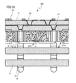
FIG. 31 is a schematic cross-sectional view of a semiconductor device 300 of the ninth embodiment;
FIG. 32 is a schematic cross-sectional view of a wiring board of Comparative Example 1;
FIG. 33 is a schematic cross-sectional view of the wiring board of Comparative Example 1 taken along line A-A′;
FIG. 34 is a schematic cross-sectional view of a wiring board of Comparative Example 2;
FIG. 35 is a schematic cross-sectional view of the wiring board of Comparative Example 2 taken along line A-A′;
FIG. 36 is a schematic cross-sectional view of a wiring board of Comparative Example 3;
FIG. 37 is a schematic cross-sectional view of the wiring board of Comparative Example 3 taken along line A-A′;
FIG. 38 is a diagram showing frequency dependencies of a scattering parameter S21 of the through via of the wiring boards of Example 1, Comparative Example 1, Comparative Example 2, and Comparative Example 3;
FIG. 39 is a diagram showing relationships between loss and a film thickness of an insulating film around the through via; and
FIG. 40 is a diagram showing a relationship between loss and a distance from a surface of the through via to the center of a second insulating film.
DETAILED DESCRIPTION
A wiring board of an embodiment includes: a through via; a first insulating film disposed around the through via; a second insulating film disposed around the first insulating film, the second insulating film having a relative permittivity lower than a relative permittivity of the first insulating film; a third insulating film disposed around the second insulating film, the third insulating film having a relative permittivity higher than the relative permittivity of the second insulating film; and a resin disposed around the third insulating film, the resin including fillers.
First Embodiment
A wiring board of the present embodiment includes: a through via; a first insulating film disposed around the through via; a second insulating film disposed around the first insulating film, the second insulating film having a relative permittivity lower than a relative permittivity of the first insulating film; a third insulating film disposed around the second insulating film, the third insulating film having a relative permittivity higher than the relative permittivity of the second insulating film; and a resin disposed around the third insulating film, the resin including fillers.
FIG. 1 is a schematic cross-sectional view of the wiring board 100 of the present embodiment. FIG. 2 is a schematic top view of the wiring board 100 of the present embodiment, and FIG. 3 is a schematic cross-sectional view of the wiring board 100 of the present embodiment taken along line A-A′.
Through a through via 10 an electric signal passes, which is sent to or from a semiconductor chip and the like disposed on the wiring board, for example. It is preferable that material of the through via 10 includes at least one type of conductor selected from the group consisting of gold (Au), silver (Ag), cupper (Cu), nickel (Ni), tungsten (W), tin (Sn), and a conductive organic substance in order to attain high conductivity.
Specifically preferable material of the through via 10 is metal such as Au, Ag, and Cu, which are generally used for electric wiring.
Other materials also can be preferably used such as Li, Be, Na, Mg, Al, K, Ca, Sc, Ti, V, Cr, Mn, Fe, Co, Zn, Ga, Rb, Sr, Y, Zr, Nb, Mo, Tc, Ru, Rh, Pd, Cd, Sn, Cs, Ba, La, Ce, Pr, Pm, Nd, Sm, Eu, Gd, Tb, Dy, Ho, Er, Tm, Yb, and Lu and an alloy of the above metals.
As conductive organic substances used for the through via 10, organic substance such as polyacetylene, poly (p-phenylene), poly (p-phenylenevinylene), polypyrrole, polythiophene, polyaniline, polythiophene, polyacene, and graphene is preferably used.
A first insulating film 12 is disposed around the through via 10, a second insulating film 14 having a relative permittivity lower than a relative permittivity of the first insulating film 12 is disposed around the first insulating film 12, and a third insulating film 16 having a relative permittivity higher than the relative permittivity of the second insulating film 14 is disposed around the second insulating film 14, respectively.
As materials for the first insulating film 12, the second insulating film 14, and the third insulating film 16, polyethylene (PE), polypropylene (PP), polytetrafluoroethylene (PTFE), polyvinyl chloride (PVC), polyvinyl alcohol (PVA), polyvinyl phenol, polyvinyl pyrrolidone (PVP), polystyrene (PS), polyacrylate, polymethylmethacrylate (PMMA), polyacrylonitrile (PAN), polycarbonate (PC), polyterephthalate ethylene (PET), parylene, polyphenylene sulfide (PPS), polyimide (PI), benzocyclobutene (BCB), cyclopentene (CyPe), polysilsesquioxane (PSQ), and SOG (Spin-On-Glass) are preferably used. Among the above materials, polyimide (PI) and SOG (Spin-On-Glass) are specifically preferably used.
It is possible to control the permittivities of the first insulating film 12, the second insulating film 14, and the third insulating film 16 by appropriately mixing a plurality of substances from the above group of substances by using a known technique, or by appropriately changing synthesis conditions by using a known technique, or the like.
Around the third insulating film 16, a filler-containing resin 20 is disposed. The filler-containing resin 20 includes filler 22 and resin 24.
The filler 22 is a filler generally used to control thermal expansion or the like, and inorganic oxide particles such as silica, alumina, aluminum nitride, boron nitride, zinc oxide, magnesium oxide, and zinc oxide and dielectric particles such as barium titanate, strontium titanate, barium strontium titanate, strontium zirconate, and bismuth zirconate are preferably used, for example. Among the above materials, silica is specifically preferably used.
As the resin 24, it is possible to preferably use, for example, a phenol resin, a polyester resin, an epoxy resin, a polyimide resin, a fluorine resin, and the like. Among the above resins, an epoxy resin is specifically preferably used. Further, when a base material to be a core of the wiring board is used, paper or glass cloth can be preferably used.
The wiring board of the present embodiment may be further provided with an electrode wiring. The electrode wiring is used for transmission of a signal or the like. The electrode wiring is disposed in contact with the surface of the through via 10 as an electrode wiring 30 or is disposed on the surface of the filler-containing resin 20 as an electrode wiring 32, for example. The electrode wiring may be also disposed inside the filler-containing resin 20.
A method of manufacturing the wiring board of the present embodiment will be described below. FIGS. 4 to 12 are schematic cross-sectional views showing the method of manufacturing the wiring board of the present embodiment, respectively. Firstly, as shown in FIG. 4, an adhesive layer 42 is formed on a support substrate 40. Next, as shown in FIG. 5, a seed layer 44 is formed on the adhesive layer 42. As the material of the seed layer, known materials can be preferably used, and Ti, Cu, Sn, Ni, Ta, and Ag are specifically preferably used. The seed layer preferably has a film thickness of not less than 1 μm. The seed layer is preferably formed by a known method such as a sputtering method, a vacuum vapor deposition method, an electroless plating method, and a sputtering method can be specifically preferably used.
Next, as shown FIG. 6, a resist 46 is applied on the surface of the seed layer 44 and is patterned by exposure to form an opening 48. Then, as shown in FIG. 7, the through via 10 is formed in the opening 48. The through via 10 is preferably formed by an electroplating method, for example.
Next, as shown in FIG. 8, the resist 46 is peeled off by organic cleaning or the like. At this time, the electrode wiring 30 and the electrode wiring 32 may be formed by using the seed layer 44, by wet etching or the like.
Next, as shown in FIG. 9, the first insulating film 12 is formed around the through via 10. Next, as shown in FIG. 10, the second insulating film 14 is formed around the first insulating film 12. Next, as shown in FIG. 11, the third insulating film 16 is formed around the second insulating film 14. It is preferable that the first insulating film 12, the second insulating film 14, and the third insulating film 16 are formed by coating by using a spin coating method.
Next, as shown in FIG. 12, the periphery is filled with the filler-containing resin 20. It is preferable that the filler-containing resin 20 is filled by a resin printing device.
Next, as shown in FIG. 13, the filled filler-containing resin 20 is planarized by resin polishing. Next, as shown in FIG. 14, on the planarized surface, the electrode wiring 30 is formed. Finally, as shown in FIG. 15, by removing the adhesive layer 42, the wiring board 100 of the present embodiment is manufactured.
For example, when a signal in a frequency band of about 1 GHz to 30 GHz passes through the through via 10, electricity flows through the through via 10, and at the same time, an electric field spreads on the surface of the through via 10 due to the skin effect of radio wave. The permittivity of the filler and the permittivity of the resin are generally different. Thus, there is a problem that, in the case that the filler-containing resin 20 is in direct contact with the periphery of the through via 10, substances having different permittivities are distributed in an area in which the radio wave spreads, whereby the radio wave is scattered and insertion loss is accordingly increased.
For example, when only one type of insulating film, which is the first insulating film 12, is disposed, it is necessary to make the film thickness of the insulating film around the through via thicker according to the expansion of the radio wave associated with an increase in power passing through. In this case, there is a problem that an advantageous effect of the thicker film thickness is about the same as that of the case in which the filler is not included even if the film thickness is made thicker.
For example, in the case that two types of the insulating films, which are the first insulating film 12 and the second insulating film 14, are disposed, it is possible to trap the radio wave in the first insulating film. As a result, compared with the case that one type of the insulating film, which is the first insulating film 12, is disposed, a high effect can be obtained even if the film thickness of the entire insulating films is made thin. However, there is a problem also in this case that the effect is about the same as in the case that the filler is not contained, even if the film thickness is made thicker.
The wiring board of the present embodiment includes: a through via; a first insulating film disposed around the through via; a second insulating film disposed around the first insulating film, the second insulating film having a relative permittivity lower than a relative permittivity of the first insulating film; a third insulating film disposed around the second insulating film, the third insulating film having a relative permittivity higher than the relative permittivity of the second insulating film; and a resin disposed around the third insulating film, the resin including fillers. With this arrangement, when an electric signal is transmitted through the through via 10, the radio wave spreading around the through via 10 is trapped in the second insulating film, whereby the insertion loss can be suppressed.
Here, the effect of suppression of the increase of the insertion loss is greater than the case of a through mold via containing no filler. It is noted that relative permittivities of insulating films can be evaluated by spectroscopic ellipsometry or a network analyzer.
In addition, it is preferable that the permittivity of the first insulating film 12 is same as the permittivity of the third insulating film 16 so that the radio wave is trapped similarly in both sides of the second insulating film 14. However, the permittivity of the first insulating film 12 may be different from the permittivity of the third insulating film 16.
It is preferable that the first insulating film 12, the second insulating film 14, and the third insulating film 16 each has a ring structure having the central axis in a direction perpendicular to the principal surface of the wiring board. In other words, it is preferable that the first insulating film 12, the second insulating film 14, and the third insulating film 16 have cylindrical shapes having through holes passing through in the direction perpendicular to the bottom surfaces of the cylindrical shapes. With this arrangement, the radio wave passing through the through via can be uniformly trapped in the direction perpendicular to the bottom surface.
It is preferable that the relative permittivity of the first insulating film and the relative permittivity of the third insulating film are not less than 2.4 and not more than 9. When an insulating film with a relative permittivity lower than 2.4 is used for the first insulating film and the third insulating film, the difference from the relative permittivity of the second insulating film is too small to successfully trap the radio wave in the second insulating film. On the other hand, generally, there is a negative correlation between the relative permittivity and a band gap of an insulating film; thus, a material with too high relative permittivity has a narrow band gap, whereby an insulation property of the insulating film deteriorates. As a result, the insertion loss can be increased.
It is preferable that the film thickness of the second insulating film is not less than 2.7% and not more than 20% of the sum of the film thickness of the first insulating film and the film thickness of the third insulating film. If the film thickness is too thin, it is not possible to trap the radio wave successfully; thus, the radio wave leaks into the first insulating film and the third insulating film. On the other hand, if the second insulating film is too thick, the radio wave spreads too much in the second insulating film, whereby the insertion loss can increase, on the contrary.
It is preferable that a ratio of (i) a difference between a distance from the inside surface of the first insulating film to the center of the film thickness of the second insulating film and a half of a distance from the inside surface of the first insulating film to the outside surface of the third insulating film to (ii) a distance from the inside surface of the first insulating film to the outside surface of the third insulating film is not more than 0.2. With this arrangement, the second insulating film is disposed approximately at the center of the entire insulating films including the first insulating film, the second insulating film, and the third insulating film, and the insertion loss due to filler can be effectively prevented further from increasing.
It is preferable that a sum of the film thickness of the first insulating film and the film thickness of the third insulating film is not less than 89% of a sum of the film thickness of the first insulating film, the film thickness of the second insulating film, and the film thickness of the third insulating film. In order to prevent the scattering of the radio wave by the filler, it is preferable that the first insulating film and the third insulating film have certain film thicknesses.
It is noted that the film thickness of the insulating film represents the film thickness in a cross-section parallel to the main surface of the wiring board in the present specification. For example, in the case of the wiring board of FIG. 1, the film thickness of the first insulating film 12 is denoted by d1. The film thickness of the second insulating film is denoted by d2. The film thickness of the third insulating film is denoted by d3.
According to the wiring board 100 of the present embodiment, with the above-described configuration, it is possible to reduce the loss in the through via and to provide a wiring board provided with a low-loss through via. In addition, by the manufacturing method of the present embodiment, it is possible to manufacture a wiring board provided with such low-loss through via.
Second Embodiment
A wiring board of the present embodiment is a wiring board of the first embodiment in which an electrode wiring is further provided, and the electrode wiring includes a strip-line. In the following description, the same points as in the first embodiment will be omitted.
FIG. 16 is a schematic cross-sectional view of a wiring board 100 of the present embodiment. FIG. 17 is a schematic top view of the wiring board 100 of the present embodiment, and FIG. 18 is a schematic cross-sectional view of the wiring board 100 of the present embodiment taken along line A-A′.
A strip-line 60 includes two electrode wirings 36 disposed on the surfaces of the wiring board 100 and an electrode wiring 34 disposed inside the wiring board 100, for example. The two electrode wirings 36 are used as ground lines, and the electrode wiring 34 is used as a signal line.
On the electrode wiring 34, there may be disposed a stub 38. The stub 38 functions as a capacitor or an inductor, depending on the size thereof.
It is noted that a form of the strip-line 60 preferably used in the present embodiment is not limited to the above-described form, and any known strip-line can be preferably used.
According to the wiring board 100 of the present embodiment, with the above-described configuration, it is possible to provide a wiring board provided with a low-loss through via 10 and the strip-line 60.
Third Embodiment
A wiring board of the present embodiment is a wiring board of the first embodiment in which an electrode wiring is further provided, and the electrode wiring includes a micro strip-line. In the following description, the same points as in the first embodiment will be omitted.
FIG. 19 is a schematic cross-sectional view of a wiring board 100 of the present embodiment. FIG. 20 is a schematic top view of the wiring board 100 of the present embodiment.
A micro strip-line 62 includes an electrode wiring 36 disposed on one surface of the wiring board 100 and an electrode wiring 34 disposed on the other surface of the wiring board 100, for example. The electrode wiring 36 is used as a ground line, and the electrode wiring 34 is used as a signal line.
The electrode wiring 34 may be also provided with a stub 38. The stub 38 functions as a capacitor or an inductor, depending on the size thereof.
It is noted that a form of the micro strip-line 62 preferably used in the present embodiment is not limited to the above-described form, and any known micro strip-line can be preferably used.
According to the wiring board 100 of the present embodiment, with the above-described configuration, it is possible to provide a wiring board 100 provided with a low-loss through via 10 and the micro strip-line 62.
Fourth Embodiment
A wiring board of the present embodiment is a wiring board of the first embodiment in which an electrode wiring is further provided, and the electrode wiring includes a coplanar line. In the following description, the same pints as in the first embodiment will be omitted.
FIG. 21 is a schematic cross-sectional view of a wiring board 100 of the present embodiment. FIG. 22 is a schematic top view of the wiring board 100 of the present embodiment.
A coplanar line 64, for example, includes two parallel electrode wirings 36 disposed on the surface of the wiring board 100 and an electrode wiring 34 disposed between the two parallel electrode wirings 36. The two parallel electrode wirings 36 are used as ground lines, and the electrode wiring 34 is used as a signal line.
On the electrode wiring 34, there may be disposed a stub 38. The stub 38 functions as a capacitor or an inductor, depending on the size thereof.
It is noted that a form of the coplanar line 64 preferably used in the present embodiment is not limited to the above-described form, and any known coplanar line can be preferably used.
According to the wiring board 100 of the present embodiment, with the above-described configuration, it is possible to provide the wiring board 100 provided with a low-loss through via 10 and the coplanar line 64.
Fifth Embodiment
A wiring board of the present embodiment is a wiring board of the first embodiment in which an electrode wiring is further provided, and the electrode wiring includes a coaxial line. In the following description, the same points as in the first embodiment will be omitted.
FIG. 23 is a schematic cross-sectional view of a wiring board 100 of the present embodiment.
A coaxial line 65 includes at least a coaxial signal line 69. The coaxial signal line 69 transmits a signal having passed through the through via 10 to another device such as a semiconductor chip.
The coaxial line 65 may further include a coaxial line insulating film 68 disposed around the coaxial signal line 69, a coaxial line ground line 67 disposed around the coaxial line insulating film 68, and a covering 66 disposed around the coaxial line ground line 67.
The coaxial line ground line 67 functions as a ground for a signal passing through the coaxial signal line 69. The coaxial line insulating film 68 electrically insulates the coaxial signal line 69 from the coaxial line ground line 67. The covering 66 is preferably disposed so that the coaxial line ground line 67 is prevented from being in electric contact with other electric components and the like.
Further, on the wiring board 100, there may be disposed an electrode wiring 36 to function as the ground and to be in electrically contact with the coaxial line ground line 67.
According to the wiring board 100 of the present embodiment, with the above-described configuration, it is possible to provide the wiring board 100 provided with the low-loss through via 10 and the coaxial line 65.
Sixth Embodiment
A wiring board of the present embodiment is a wiring board of the first embodiment in which an electrode wiring is further provided, and at least one selected from the group consisting of the electrode wiring, a first insulating film, a second insulating film, and a third insulating film includes a capacitor. In the following description, overlapped parts as in the first embodiment will be omitted.
FIG. 24 is a schematic cross-sectional view of a wiring board 100 of the present embodiment. FIG. 25 is a schematic top view of the wiring board 100 of the present embodiment.
A capacitor 50, for example, includes a plurality of electrode wirings 30 and a dielectric film 58 disposed between the electrode wirings 30, for example. It is noted that a form of the capacitor 50 preferably used in the present embodiment is not limited to the above-described form, and any known capacitor can be preferably used.
According to the wiring board 100 of the present embodiment, with the above-described configuration, it is possible to provide the wiring board 100 provided with through via 10 having small insertion loss and the capacitor 50.
Seventh Embodiment
A wiring board of the present embodiment is a wiring board of the first embodiment in which an electrode wiring is further provided, and at least one selected from the group consisting of the electrode wiring, a first insulating film, a second insulating film, and a third insulating film includes a resistor. In the following description, overlapped parts as in the first embodiment will be omitted.
FIG. 26 is a schematic cross-sectional view of a wiring board 100 of the present embodiment. FIG. 27 is a schematic top view of the wiring board 100 of the present embodiment.
A resistor 52, for example, includes an electrode wiring 30 having a plurality of bent portions. It is noted that a form of the resistor 52 preferably used in the present embodiment is not limited to the above-described form, and any known resistor can be preferably used.
According to the wiring board 100 of the present embodiment, with the above-described configuration, it is possible to provide the wiring board 100 provided with a through via 10 having small insertion loss and the resistor 52.
Eighth Embodiment
A wiring board of the present embodiment is a wiring board of the first embodiment in which an electrode wiring is further provided, and at least one selected from the group consisting of the electrode wiring, a first insulating film, a second insulating film, and a third insulating film includes an inductor. In the following description, overlapped parts as in the first embodiment will be omitted.
FIG. 28 is a schematic cross-sectional view of a wiring board 100 of the present embodiment. FIG. 29 is a schematic top view of the wiring board 100 of the present embodiment.
An inductor 54, for example, includes, as shown in FIG. 29, an electrode wiring having a plurality of bent portions disposed on the surface of the wiring board and an electrode wiring disposed in the wiring board and used to take out electricity from the inner part of an electrode wiring, for example. It is noted that a form of the inductor 54 preferably used in the present embodiment is not limited to the above-described form, and any known inductor can be preferably used.
According to the wiring board 100 of the present embodiment, with the above-described configuration, it is possible to provide the wiring board 100 provided with a through via 10 having small insertion loss and the inductor 54.
Ninth Embodiment
A semiconductor device of the present embodiment is provided with (i) a chip-scale package provided with the wiring board of any one of the first to eighth embodiments and a semiconductor chip, (ii) a package substrate, and (iii) solder balls disposed between the chip-scale package and the package substrate. In the following description, overlapped parts as in the first to eighth embodiments will be omitted.
FIG. 30 is a schematic cross-sectional view of a wiring board 200 used in the present embodiment. FIG. 31 is a schematic cross-sectional view of a semiconductor device 300 of the present embodiment.
The chip-scale package is also called a chip-size package and is generally a package provided with a chip such as a semiconductor chip. In particular, a chip-scale package in which a part of a semiconductor substrate is exposed is sometimes called a wafer-level chip-scale package or simply called a wafer-level package.
The semiconductor device 300 may be provided with a rewiring layer 78 as shown in FIG. 31.
A method of manufacturing the semiconductor device 300 of the present embodiment will be described below. A semiconductor chip 70 is mounted on an adhesive layer (not shown) by using a flip chip bonder or the like.
The rewiring layer 78 is formed by performing the following steps in order: applying polyimide; patterning by exposure, setting by curing, surface cleaning by ashing, and forming a wiring layer. As a material for wiring, titanium (Ti), nickel (Ni), aluminum (Al), silver (Ag), gold (Au), cupper (Cu), tungsten (W), and the like are preferably used. A component 80 is mounted by a flip bonder or the like after the rewiring layer 78 is formed.
Next, the package substrate 72 and the chip-scale package 250 are made to face each other, and a first conductive junction structure is formed on the surface of the chip-scale package 250 facing the package substrate 72. In addition, a second conductive junction structure is joined on the surface of the package substrate 72 facing the chip-scale package 250.
For example, the first conductive junction structure includes a solder ball 74, and the second conductive junction structure includes a pad electrode 76. To the contrary, of course, the first conductive junction structure may include a pad electrode 76, and the second conductive junction structure may include a solder ball 74, for example.
As a solder for the solder ball 74, used known solders can be used, such as Pb-based solder, Sn-based solder, or the like. Sn—Ag—Cu-based solder is easy to use and since it is cheap, and can thus be specifically preferably used.
Finally, the surface of the chip-scale package 250 facing the package substrate 72 and the surface of the package substrate 72 facing the chip-scale package 250 are joined. This joining is performed by a flip chip bonder or the like by using the solder ball 74 and the like.
The total layer number of the stacked package substrates 72 and chip-scale package 250 is preferably three. However, the order of the manufacturing method is not limited to the above process. For example, in the present embodiment, the component 80 is mounted on the chip-scale package 250 as a mounting step before the package substrate 72 is bonded; however, the order is not limited thereto.
EXAMPLES
An example will be described below in detail while comparing with comparative examples.
Example 1
A wiring board 100 shown in FIG. 1 was manufactured. The through via 10, the electrode wiring 30, and the electrode wiring 32 were made of Cu, and the first insulating film 12, the second insulating film 14, and the third insulating film 16 were made of SOG. As the filler 22, silica was used, and as the resin 24, an epoxy resin was used. The film thickness of the substrate was 400 μm.
Comparative Example 1
A wiring board 100 was manufactured similarly as the wiring board 100 of Example 1. FIG. 32 is a schematic cross-sectional view of the wiring board 100 of this comparative example. FIG. 33 is a schematic cross-sectional view of the wiring board 100 of this comparative example taken along line A-A′. In this wiring board 100, the filler-containing resin 20 was in direct contact with the periphery of the through via 10. The film thickness of the substrate was 400 μm.
Comparative Example 2
A wiring board 100 was manufactured similarly to that of the wiring board 100 of Example 1. FIG. 34 is a schematic cross-sectional view of the wiring board 100 of this comparative example. FIG. 35 is a schematic cross-sectional view of the wiring board of this comparative example taken along line A-A′. In this wiring board 100, the first insulating film 12 is disposed around the through via 10, and the filler-containing resin 20 is dispose around the first insulating film 12. The film thickness of the substrate was 400 μm.
Comparative Example 3
A wiring board 100 was manufactured similarly to that of the wiring board 100 of Example 1. FIG. 36 is a schematic cross-sectional view of the wiring board 100 of this comparative example. FIG. 37 is a schematic cross-sectional view of the wiring board of this comparative example taken along line A-A′. In this wiring board 100, the first insulating film 12 is disposed around the through via 10, and the second insulating film 14 is disposed around the first insulating film 12, and the filler-containing resin 20 is disposed around the second insulating film 14. The film thickness of the substrate was 400 μm.
FIG. 38 is a diagram showing the frequency dependencies of scattering parameters S21 of the through vias of the wiring boards of Example 1, Comparative Example 1, Comparative Example 2, and Comparative Example 3. Assuming the case that the effects of Comparative Example 1, Comparative Example 2, and Comparative Example 3 were maximized, the results were estimated. The estimated results are denoted by Coaxial TMV (∈=2.0) and Coaxial TMV (∈=3.6) in the graph. Each of the diameters of the through vias here was 20 μm. In Comparative Example 2, the film thickness of the first insulating film was 8 μm. In Comparative Example 3, the film thickness of the first insulating film was 8 μm, and the film thickness of the second insulating film was 1.5 μm. In Example 1, the film thickness of the first insulating film was 10 μm, the film thickness of the second insulating film was 2 μm, and the film thickness of the third insulating film was 10 μm. Further, the relative permittivity of the first insulating film and the relative permittivity of the third insulating film were both 3.5, and the relative permittivity of the second insulating film was 2.4. Regarding the through via of Example 1, the insertion loss is lowest especially in the signal frequency band of 10 GHz to 30 GHz.
In the wiring board of Comparative Example 1, an electric field spreads on the surface of the through via due to the skin effect of radio wave while electricity is flowing through the through via. Thus, since the two types of substances, the filler 22 and the resin 24, having different permittivities are distributed in the area in which the radio wave spreads, the radio wave is scattered, whereby the insertion loss is large.
In the wiring board of Comparative Example 2, the radio wave spreads around the through via in the same way as in the case of the through via of the wiring board of Comparative Example 1. However, because the first insulating film having a uniform permittivity is disposed around the through via, the scattering loss due to filler is reduced. However, in order to achieve sufficient effect, it is preferable to make the film thickness of the insulating film thicker depending on how much the radio wave spreads. However, there is a problem that, even if the film thickness is made thicker, the advantageous effect of the thicker film thickness is at most the same as in the case that an effect of the increase in the scattering due to the filler contained in the resin is not included.
In the wiring board of Comparative Example 3, the radio wave can be trapped in the second insulating film. Thus, when the film thickness of the insulating film is made thin, sufficiently advantageous effect can be obtained compared with the wiring board of Comparative Example 2. However, even in the case of Comparative Example 3, there is a problem that, even if the film thickness is made thicker, the advantageous effect is about the same as in the case that no filler is contained.
In the wiring board of Example 1, the radio wave generated when an electric signal is transmitted to the through via can be trapped in the insulating ring having a lower permittivity. As a result, scattering due to filler can be prevented, whereby insertion loss can be lower. Further, the advantageous effect can realize a lower loss compared with the through mold via containing no filler.
FIG. 39 is a diagram showing a relationship between the film thickness of the insulating film covering the periphery of the through via and the loss. The frequency is 10 GHz. Here, regarding Comparative Example 2 and Comparative Example 3, the graph shows the loss (scattering parameter S21) in relation to the film thickness of the first insulating film. Regarding Example 1, the graph shows the loss (scattering parameter S21) in relation to the sum of the film thickness of the first insulating film and the film thickness of the third insulating film.
In Example 1, the film thickness of the first insulating film and the film thickness of the third insulating film are equal to each other, which means that the second insulating film is disposed at the center of the first insulating film and the third insulating film. In addition, the film thicknesses of the second insulating films of Comparative Example 3 and Example 1 are 2 μm.
Regarding Comparative Example 2, it can be seen that the loss tends to decrease with increase in the thickness of the first insulating film. The effect is saturated when the film thickness is approximately 30 μm or more. Also regarding Comparative Example 3, the loss decreases with increase in the thickness of the first insulating film. Comparative Example 3 is also effective when the film thickness of the insulating film is thinner than that of Comparative Example 2.
When the sum of the film thicknesses of the first insulating film and the third insulating film is not more than 5 μm, Example 1 is less effective than Comparative Example 2 and Comparative Example 3; however, when the sum is greater than 10 μm, the loss is smaller than those of the former two structures, and when the thickness is 16 μm or more, the loss is saturated. Thus, because a sum of the film thickness of the first insulating film, the film thickness of the second insulating film, and the film thickness of the third insulating film is not less than 18 μm at this time, it is preferable that the sum of the film thickness of the first insulating film and the film thickness of the third insulating film is not less than 89% of the sum of the film thickness of the first insulating film, the film thickness of the second insulating film, and the film thickness of the third insulating film. Further, this advantageous effect is obtained when the second insulating film is disposed at the center of the entire insulating films.
FIG. 40 shows the relationship between the distance from the surface of the through via to the center of the second insulating film and the loss. The frequency is 10 GHz. The film thickness of the entire insulating films is made 30 μm, and the center is thus 15 μm. From this result, it can be understood that the advantageous effects is greater when the second insulating film is located closer to the center of the entire insulating films.
For this reason, it is preferable that the center of the film thickness of the second insulating film is located within ±5 μm of approximately the center of the film thickness (30 μm) of the entire insulating films; thus, a ratio of (i) a difference between a distance from the inside surface of the first insulating film to the center of the film thickness of the second insulating film and a half of a distance from the inside surface of the first insulating film to the outside surface of the third insulating film to (ii) a distance from the inside surface of the first insulating film to the outside surface of the third insulating film is not more than 0.2.
The wiring board of at least one of the above-described embodiments includes: a through via; a first insulating film disposed around the through via; a second insulating film disposed around the first insulating film, the second insulating film having a relative permittivity lower than a relative permittivity of the first insulating film; a third insulating film disposed around the second insulating film, the third insulating film having a relative permittivity higher than the relative permittivity of the second insulating film; and a resin disposed around the third insulating film, the resin including fillers, and thus it is possible to reduce the loss in the through via and to provide a wiring board provided with a low-loss through via.
While certain embodiments have been described, these embodiments have been presented by way of example only, and are not intended to limit the scope of the inventions. Indeed, the wiring board and the method of manufacturing the same described herein may be embodied in a variety of other forms; furthermore, various omissions, substitutions and changes in the form of the devices and methods described herein may be made without departing from the spirit of the inventions. The accompanying claims and their equivalents are intended to cover such forms or modifications as would fall within the scope and spirit of the inventions.

Claims (15)

What is claimed is:
1. A wiring board comprising:
a through via;
a first insulating film disposed around the through via;
a second insulating film disposed around the first insulating film, the second insulating film having a relative permittivity lower than a relative permittivity of the first insulating film;
a third insulating film disposed around the second insulating film, the third insulating film having a relative permittivity higher than the relative permittivity of the second insulating film; and
a resin disposed around the third insulating film, the resin including fillers.
2. The wiring board according to claim 1, wherein the relative permittivity of the first insulating film and the relative permittivity of the third insulating film are not less than 2.4 and not more than 9.
3. The wiring board according to claim 1, wherein a film thickness of the second insulating film is not less than 2.7% and not more than 20% of a sum of a film thickness of the first insulating film and a film thickness of the third insulating film.
4. The wiring board according to claim 1, wherein a ratio of (i) a difference between a distance from an inside surface of the first insulating film to a center of the film thickness of the second insulating film and a half of a distance from the inside surface of the first insulating film to an outside surface of the third insulating film to (ii) the distance from the inside surface of the first insulating film to the outside surface of the third insulating film is not more than 0.2.
5. The wiring board according to claim 1, wherein a sum of the film thickness of the first insulating film and the film thickness of the third insulating film is not less than 89% of a sum of the film thickness of the first insulating film, a film thickness of the second insulating film, and the film thickness of the third insulating film.
6. The wiring board according to claim 1, wherein the through via includes at least one type of conductor selected from a group consisting of Au, Ag, Cu, Ni, W, Sn, and a conductive organic substance.
7. The wiring board according to claim 1, further comprising an electrode wiring disposed on or inside the resin.
8. The wiring board according to claim 7, wherein the electrode wiring includes at least one type of transmission line selected from a group consisting of a strip-line, a micro strip-line, a coplanar line, and a coaxial line.
9. The wiring board according to claim 7, wherein at least one selected from the electrode wiring, the first insulating film, the second insulating film, and the third insulating film constitutes at least one type of electric component selected from a group consisting of a capacitor, a resistor, and an inductor.
10. A method of manufacturing a wiring board, the method comprising:
forming a through via;
forming a first insulating film around the through via;
forming, around the first insulating film, a second insulating film having a relative permittivity lower than a relative permittivity of the first insulating film;
forming, around the second insulating film, a third insulating film having a relative permittivity higher than the relative permittivity of the second insulating film; and
forming a resin around the third insulating film, the resin including fillers.
11. The method according to claim 10, wherein the relative permittivity of the first insulating film and the relative permittivity of the third insulating film are not less than 2.4 and not more than 9.
12. The method according to claim 10, wherein a film thickness of the second insulating film is not less than 2.7% and not more than 20% of a sum of a film thickness of the first insulating film and a film thickness of the third insulating film.
13. The method according to claim 10, wherein a ratio of (i) a difference between a distance from an inside surface of the first insulating film to a center of the film thickness of the second insulating film and a half of a distance from the inside surface of the first insulating film to an outside surface of the third insulating film to (ii) the distance from the inside surface of the first insulating film to the outside surface of the third insulating film is not more than 0.2.
14. The method according to claim 10, wherein a sum of the film thickness of the first insulating film and the film thickness of the third insulating film is not less than 89% of a sum of the film thickness of the first insulating film, a film thickness of the second insulating film, and the film thickness of the third insulating film.
15. The method according to claim 10, wherein the through via includes at least one type of conductor selected from a group consisting of Au, Ag, Cu, Ni, W, Sn, and a conductive organic substance.
US14/585,657 2014-01-10 2014-12-30 Wiring board and method of manufacturing the same Active 2036-12-11 US9913367B2 (en)

Applications Claiming Priority (2)

Application Number Priority Date Filing Date Title
JP2014-003365 2014-01-10
JP2014003365A JP6165640B2 (en) 2014-01-10 2014-01-10 Wiring board and manufacturing method thereof

Publications (2)

Publication Number Publication Date
US20150201488A1 US20150201488A1 (en) 2015-07-16
US9913367B2 true US9913367B2 (en) 2018-03-06

Family

ID=53522584

Family Applications (1)

Application Number Title Priority Date Filing Date
US14/585,657 Active 2036-12-11 US9913367B2 (en) 2014-01-10 2014-12-30 Wiring board and method of manufacturing the same

Country Status (2)

Country Link
US (1) US9913367B2 (en)
JP (1) JP6165640B2 (en)

Families Citing this family (2)

* Cited by examiner, † Cited by third party
Publication number Priority date Publication date Assignee Title
KR102013884B1 (en) * 2017-12-20 2019-08-23 전자부품연구원 Semiconductor package and manufacturing method thereof
CN111010797A (en) 2018-10-08 2020-04-14 中兴通讯股份有限公司 Circuit board, equipment and via hole forming method

Citations (18)

* Cited by examiner, † Cited by third party
Publication number Priority date Publication date Assignee Title
US4985600A (en) * 1988-09-30 1991-01-15 Siemens Aktiengesellschaft Printed circuit board having an injection molded substrate
JPH0897525A (en) 1994-07-13 1996-04-12 Hitachi Ltd Wiring structure and it manufacture
JPH11204945A (en) 1998-01-12 1999-07-30 Nec Niigata Ltd Multilayer wiring board
JP2003060115A (en) 2001-08-20 2003-02-28 Fujitsu Ltd Circuit board with built-in capacitor and method for manufacturing the same
US6884313B2 (en) 2001-01-08 2005-04-26 Fujitsu Limited Method and system for joining and an ultra-high density interconnect
JP2005159268A (en) 2003-10-29 2005-06-16 Kyocera Corp Wiring substrate and its manufacturing method
JP2007234715A (en) 2006-02-28 2007-09-13 Nec Corp Multilayer printed circuit board
JP2009239147A (en) 2008-03-28 2009-10-15 Toshiba Corp Integrated semiconductor device, and integrated three-dimensional semiconductor device
JP2010040721A (en) 2008-08-04 2010-02-18 Sanyo Electric Co Ltd Semiconductor module, semiconductor device, portable apparatus, and manufacturing method of semiconductor module, and manufacturing method of semiconductor device
JP2010067623A (en) 2008-09-08 2010-03-25 Shinko Electric Ind Co Ltd Board with built-in chip and method for manufacturing the same
US20100244059A1 (en) 2009-03-30 2010-09-30 Kabushiki Kaisha Toshiba Semiconductor device and manufacturing method thereof
US8164920B2 (en) * 2005-06-13 2012-04-24 Ibiden Co., Ltd. Printed wiring board
US8174840B2 (en) * 2006-01-13 2012-05-08 Industrial Technology Research Institute Multi-functional composite substrate structure
US20120228755A1 (en) 2011-03-08 2012-09-13 Kabushiki Kaisha Toshiba Semiconductor module and manufacturing method thereof
JP2012216601A (en) 2011-03-31 2012-11-08 Fujitsu Ltd Electronic device manufacturing method and electronic device
JP2013058545A (en) 2011-09-07 2013-03-28 Fujitsu Ltd Electronic device and manufacturing method of the same
US8730429B2 (en) * 2009-11-23 2014-05-20 Lg Display Co., Ltd. Multi-layer printed circuit board and liquid crystal display device having the same
US8766101B2 (en) * 2011-09-07 2014-07-01 Shinko Electric Industries Co., Ltd. Wiring substrate, method for manufacturing wiring substrate, and semiconductor package including wiring substrate

Patent Citations (20)

* Cited by examiner, † Cited by third party
Publication number Priority date Publication date Assignee Title
US4985600A (en) * 1988-09-30 1991-01-15 Siemens Aktiengesellschaft Printed circuit board having an injection molded substrate
JPH0897525A (en) 1994-07-13 1996-04-12 Hitachi Ltd Wiring structure and it manufacture
JPH11204945A (en) 1998-01-12 1999-07-30 Nec Niigata Ltd Multilayer wiring board
US6884313B2 (en) 2001-01-08 2005-04-26 Fujitsu Limited Method and system for joining and an ultra-high density interconnect
JP2003060115A (en) 2001-08-20 2003-02-28 Fujitsu Ltd Circuit board with built-in capacitor and method for manufacturing the same
JP2005159268A (en) 2003-10-29 2005-06-16 Kyocera Corp Wiring substrate and its manufacturing method
US8164920B2 (en) * 2005-06-13 2012-04-24 Ibiden Co., Ltd. Printed wiring board
US8174840B2 (en) * 2006-01-13 2012-05-08 Industrial Technology Research Institute Multi-functional composite substrate structure
JP2007234715A (en) 2006-02-28 2007-09-13 Nec Corp Multilayer printed circuit board
JP2009239147A (en) 2008-03-28 2009-10-15 Toshiba Corp Integrated semiconductor device, and integrated three-dimensional semiconductor device
JP2010040721A (en) 2008-08-04 2010-02-18 Sanyo Electric Co Ltd Semiconductor module, semiconductor device, portable apparatus, and manufacturing method of semiconductor module, and manufacturing method of semiconductor device
JP2010067623A (en) 2008-09-08 2010-03-25 Shinko Electric Ind Co Ltd Board with built-in chip and method for manufacturing the same
US20100244059A1 (en) 2009-03-30 2010-09-30 Kabushiki Kaisha Toshiba Semiconductor device and manufacturing method thereof
JP2010232577A (en) 2009-03-30 2010-10-14 Toshiba Corp Semiconductor device and method of manufacturing the same
US8730429B2 (en) * 2009-11-23 2014-05-20 Lg Display Co., Ltd. Multi-layer printed circuit board and liquid crystal display device having the same
US20120228755A1 (en) 2011-03-08 2012-09-13 Kabushiki Kaisha Toshiba Semiconductor module and manufacturing method thereof
JP2012190855A (en) 2011-03-08 2012-10-04 Toshiba Corp Semiconductor module and method of manufacturing the same
JP2012216601A (en) 2011-03-31 2012-11-08 Fujitsu Ltd Electronic device manufacturing method and electronic device
JP2013058545A (en) 2011-09-07 2013-03-28 Fujitsu Ltd Electronic device and manufacturing method of the same
US8766101B2 (en) * 2011-09-07 2014-07-01 Shinko Electric Industries Co., Ltd. Wiring substrate, method for manufacturing wiring substrate, and semiconductor package including wiring substrate

Also Published As

Publication number Publication date
JP2015133379A (en) 2015-07-23
US20150201488A1 (en) 2015-07-16
JP6165640B2 (en) 2017-07-19

Similar Documents

Publication Publication Date Title
US20220384958A1 (en) Antenna device
KR101568875B1 (en) Semiconductor Device and Method of Forming Integrated Passive Device Module
US10130302B2 (en) Via and trench filling using injection molded soldering
TWI489606B (en) System-in-package having integrated passive devices and method therefor
US8476115B2 (en) Semiconductor device and method of mounting cover to semiconductor die and interposer with adhesive material
US9591767B2 (en) Component built-in board and method of manufacturing the same, and component built-in board mounting body
US20170033026A1 (en) Semiconductor Device and Method of Forming Small Z Semiconductor Package
US10403567B2 (en) Fabrication method of electronic package
US8997344B2 (en) Method for manufacturing interposer
CN102208384A (en) A semiconductor structure and a forming method for a semiconductor device
US9913367B2 (en) Wiring board and method of manufacturing the same
Ostmann et al. Realization of a stackable package using chip in polymer technology
US11342267B2 (en) Semiconductor package structure and method for forming the same
JP4380551B2 (en) Semiconductor device and manufacturing method thereof
JP2006216767A (en) Semiconductor device and its manufacturing method
US20230062499A1 (en) Method forming a semiconductor package device
US11018040B2 (en) Carrier assisted substrate method of manufacturing an electronic device and electronic device produced thereby
US20240136268A1 (en) Composite component
JP2011171498A (en) Flip-chip mounting device and method of manufacturing the same

Legal Events

Date Code Title Description
AS Assignment

Owner name: KABUSHIKI KAISHA TOSHIBA, JAPAN

Free format text: ASSIGNMENT OF ASSIGNORS INTEREST;ASSIGNORS:MANAGAKI, NOBUTO;SASAKI, TADAHIRO;IIDA, ATSUKO;AND OTHERS;SIGNING DATES FROM 20141215 TO 20141226;REEL/FRAME:034993/0305

STCF Information on status: patent grant

Free format text: PATENTED CASE

MAFP Maintenance fee payment

Free format text: PAYMENT OF MAINTENANCE FEE, 4TH YEAR, LARGE ENTITY (ORIGINAL EVENT CODE: M1551); ENTITY STATUS OF PATENT OWNER: LARGE ENTITY

Year of fee payment: 4