US9842836B2 - Diode - Google Patents
Diode Download PDFInfo
- Publication number
- US9842836B2 US9842836B2 US15/097,933 US201615097933A US9842836B2 US 9842836 B2 US9842836 B2 US 9842836B2 US 201615097933 A US201615097933 A US 201615097933A US 9842836 B2 US9842836 B2 US 9842836B2
- Authority
- US
- United States
- Prior art keywords
- semiconductor layer
- layer
- conductivity type
- diode
- schottky
- Prior art date
- Legal status (The legal status is an assumption and is not a legal conclusion. Google has not performed a legal analysis and makes no representation as to the accuracy of the status listed.)
- Active
Links
Images


Classifications
-
- H01L27/0814—
-
- H—ELECTRICITY
- H10—SEMICONDUCTOR DEVICES; ELECTRIC SOLID-STATE DEVICES NOT OTHERWISE PROVIDED FOR
- H10D—INORGANIC ELECTRIC SEMICONDUCTOR DEVICES
- H10D84/00—Integrated devices formed in or on semiconductor substrates that comprise only semiconducting layers, e.g. on Si wafers or on GaAs-on-Si wafers
- H10D84/201—Integrated devices formed in or on semiconductor substrates that comprise only semiconducting layers, e.g. on Si wafers or on GaAs-on-Si wafers characterised by the integration of only components covered by H10D1/00 or H10D8/00, e.g. RLC circuits
- H10D84/204—Integrated devices formed in or on semiconductor substrates that comprise only semiconducting layers, e.g. on Si wafers or on GaAs-on-Si wafers characterised by the integration of only components covered by H10D1/00 or H10D8/00, e.g. RLC circuits of combinations of diodes or capacitors or resistors
- H10D84/221—Integrated devices formed in or on semiconductor substrates that comprise only semiconducting layers, e.g. on Si wafers or on GaAs-on-Si wafers characterised by the integration of only components covered by H10D1/00 or H10D8/00, e.g. RLC circuits of combinations of diodes or capacitors or resistors of only diodes
-
- H01L29/36—
-
- H01L29/866—
-
- H01L29/872—
-
- H—ELECTRICITY
- H10—SEMICONDUCTOR DEVICES; ELECTRIC SOLID-STATE DEVICES NOT OTHERWISE PROVIDED FOR
- H10D—INORGANIC ELECTRIC SEMICONDUCTOR DEVICES
- H10D62/00—Semiconductor bodies, or regions thereof, of devices having potential barriers
- H10D62/10—Shapes, relative sizes or dispositions of the regions of the semiconductor bodies; Shapes of the semiconductor bodies
- H10D62/129—Cathode regions of diodes
-
- H—ELECTRICITY
- H10—SEMICONDUCTOR DEVICES; ELECTRIC SOLID-STATE DEVICES NOT OTHERWISE PROVIDED FOR
- H10D—INORGANIC ELECTRIC SEMICONDUCTOR DEVICES
- H10D62/00—Semiconductor bodies, or regions thereof, of devices having potential barriers
- H10D62/60—Impurity distributions or concentrations
-
- H—ELECTRICITY
- H10—SEMICONDUCTOR DEVICES; ELECTRIC SOLID-STATE DEVICES NOT OTHERWISE PROVIDED FOR
- H10D—INORGANIC ELECTRIC SEMICONDUCTOR DEVICES
- H10D8/00—Diodes
- H10D8/20—Breakdown diodes, e.g. avalanche diodes
- H10D8/25—Zener diodes
-
- H—ELECTRICITY
- H10—SEMICONDUCTOR DEVICES; ELECTRIC SOLID-STATE DEVICES NOT OTHERWISE PROVIDED FOR
- H10D—INORGANIC ELECTRIC SEMICONDUCTOR DEVICES
- H10D8/00—Diodes
- H10D8/60—Schottky-barrier diodes
-
- H01L29/0619—
-
- H01L29/47—
-
- H—ELECTRICITY
- H10—SEMICONDUCTOR DEVICES; ELECTRIC SOLID-STATE DEVICES NOT OTHERWISE PROVIDED FOR
- H10D—INORGANIC ELECTRIC SEMICONDUCTOR DEVICES
- H10D62/00—Semiconductor bodies, or regions thereof, of devices having potential barriers
- H10D62/10—Shapes, relative sizes or dispositions of the regions of the semiconductor bodies; Shapes of the semiconductor bodies
- H10D62/102—Constructional design considerations for preventing surface leakage or controlling electric field concentration
- H10D62/103—Constructional design considerations for preventing surface leakage or controlling electric field concentration for increasing or controlling the breakdown voltage of reverse-biased devices
- H10D62/105—Constructional design considerations for preventing surface leakage or controlling electric field concentration for increasing or controlling the breakdown voltage of reverse-biased devices by having particular doping profiles, shapes or arrangements of PN junctions; by having supplementary regions, e.g. junction termination extension [JTE]
- H10D62/106—Constructional design considerations for preventing surface leakage or controlling electric field concentration for increasing or controlling the breakdown voltage of reverse-biased devices by having particular doping profiles, shapes or arrangements of PN junctions; by having supplementary regions, e.g. junction termination extension [JTE] having supplementary regions doped oppositely to or in rectifying contact with regions of the semiconductor bodies, e.g. guard rings with PN or Schottky junctions
-
- H—ELECTRICITY
- H10—SEMICONDUCTOR DEVICES; ELECTRIC SOLID-STATE DEVICES NOT OTHERWISE PROVIDED FOR
- H10D—INORGANIC ELECTRIC SEMICONDUCTOR DEVICES
- H10D64/00—Electrodes of devices having potential barriers
- H10D64/60—Electrodes characterised by their materials
- H10D64/64—Electrodes comprising a Schottky barrier to a semiconductor
Definitions
- the present invention relates to a Schottky barrier diode having a Zener diode incorporated therein.
- an alternator AC generator
- an alternating current generated in a coil is rectified by a diode and taken out as a direct current.
- a Zener diode, Schottky barrier diode, etc. are known as examples of the rectifying element used (for example, Patent Document 1 (Japanese Patent Application Publication No. 2011-234614)).
- a embodiment of the present invention provides a diode, which, while having a sufficient load dump tolerance due to including a Zener diode region, is capable of realizing a low forward voltage (low VF) and a low reverse leakage current (low IR) in comparison to conventional arts.
- FIG. 1 is a circuit diagram of an alternator.
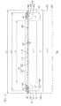
- FIG. 2 is a schematic sectional view of a diode having a JBS structure according to the present invention.
- FIG. 3 is a plan view for describing a positional configuration of p + type regions of the diode of FIG. 2 .
- FIG. 4 is a graph showing simulation results of VF-IF characteristics of the diode of FIG. 2 according to epi thickness.
- FIG. 5 is a graph showing simulation results (with epi thickness fixed) of VF-IF characteristics of the diode of FIG. 2 according to distance (distance between Xj) between mutually adjacent p + type regions.
- FIG. 6 is a graph showing a relationship of epi thickness with VF of the diode of FIG. 2 according to cell pitch.
- FIG. 7 is a graph showing a relationship of epi thickness with IR of the diode of FIG. 2 according to cell pitch.
- FIG. 8 is a graph showing a relationship of cell pitch with VF of the diode of FIG. 2 according to epi thickness.
- FIG. 9 is a graph showing a relationship of cell pitch with IR of the diode of FIG. 2 according to epi thickness.
- FIG. 10 is a graph showing a relationship of specific resistance with BV of the diode of FIG. 2 according to epi thickness.
- FIG. 11 is a graph showing a relationship of VF with IR of the diode of FIG. 2 according to cell pitch.
- FIG. 12 is a graph showing a relationship of ambient temperature with IR of the diode of FIG. 2 according to epi thickness.
- FIG. 13 is a schematic sectional view of a diode having a double epitaxial structure.
- FIG. 14 is a graph showing the VF-IF characteristics of an experimental example (Sample 1) of the diode.
- FIG. 15 is a graph showing VR-IR characteristics of Sample 1.
- FIG. 16 is a graph showing temperature characteristics of VF-IF of Sample 1.
- FIG. 17 is a graph showing temperature characteristics of VR-IR of Sample 1.
- FIG. 18 is a table showing evaluation results of Sample 1.
- FIG. 19 is a diagram for describing serial resistances inside an epitaxial layer of Sample 1.
- FIG. 20 is a concentration profile of an n type layer of Sample 1.
- FIG. 21 is a concentration profile of a p type layer of Sample 1.
- FIG. 22 is a graph showing VF-IF characteristics (simulation) of Sample 1.
- FIG. 23 is a graph showing a relationship of VF with epi thickness prepared based on the simulation.
- FIG. 24 is a graph showing VR-IR characteristics (simulation) of Sample 1.
- FIG. 25 is a table showing evaluation results of the simulation.
- a embodiment of the present invention provides a diode that includes a semiconductor layer of a first conductivity type having an impurity concentration of 1 ⁇ 10 16 cm ⁇ 3 to 2.4 ⁇ 10 17 cm ⁇ 3 , a Zener diode region of a second conductivity type formed selectively in the semiconductor layer and forming a pn junction with the semiconductor layer, a Schottky metal disposed on the semiconductor layer, forming a Schottky junction with the semiconductor layer, and having a work function of 3 eV to 6 eV, and a JBS (junction barrier Schottky) structure including a plurality of second conductivity type regions formed selectively in the Schottky junction region of the semiconductor layer.
- a semiconductor layer of a first conductivity type having an impurity concentration of 1 ⁇ 10 16 cm ⁇ 3 to 2.4 ⁇ 10 17 cm ⁇ 3
- a Zener diode region of a second conductivity type formed selectively in the semiconductor layer and forming a pn junction with the semiconductor layer
- a embodiment of the present invention provides a diode that includes a semiconductor layer of a first conductivity type having a specific resistance of 50 m ⁇ cm to 500 m ⁇ cm, a Zener diode region of a second conductivity type formed selectively in the semiconductor layer and forming a pn junction with the semiconductor layer, a Schottky metal disposed on the semiconductor layer, forming a Schottky junction with the semiconductor layer, and having a work function of 3 eV to 6 eV, and a JBS (junction barrier Schottky) structure including a plurality of second conductivity type regions formed selectively in the Schottky junction region of the semiconductor layer.
- a JBS junction barrier Schottky
- the impurity concentration of the semiconductor layer is, for example, 1 ⁇ 10 16 cm ⁇ 3 to 2.4 ⁇ 10 17 cm ⁇ 3 , more preferably 1.8 ⁇ 10 16 cm 3 to 2.4 ⁇ 10 17 cm ⁇ 3 , and even more preferably 1.8 ⁇ 10 16 cm ⁇ 3 to 8.0 ⁇ 10 16 cm ⁇ 3 .
- the specific resistance of the semiconductor layer is, for example, 50 m ⁇ cm to 500 m ⁇ cm, more preferably 50 m ⁇ cm to 300 m ⁇ cm, and even more preferably 100 m ⁇ cm to 300 m ⁇ cm.
- the work function of the Schottky metal is, for example, 3 eV to 6 eV, more preferably 4 eV to 6 eV, even more preferably 5 eV to 6 eV, and especially preferably 5.3 eV to 6 eV.
- the Schottky metal includes of Pt or Mo.
- the semiconductor layer has a thickness, for example, of 2 ⁇ m to 10 ⁇ m, more preferably 2 ⁇ m to 6 ⁇ m, and even more preferably 2.5 ⁇ m to 5 ⁇ m.
- each of the second conductivity type regions has a width W 1 of, for example, 0.1 ⁇ m to 10 ⁇ m, more preferably 1 ⁇ m to 5 ⁇ m, and even more preferably 1 ⁇ m to 2 ⁇ m.
- the plurality of second conductivity type regions are arrayed at a pitch P 1 of, for example, 2 ⁇ m to 5 ⁇ m, more preferably 2.5 ⁇ m to 4.5 ⁇ m, and even more preferably 3 ⁇ m to 4 ⁇ m.
- the plurality of second conductivity type regions are arrayed so that there is a distance D 1 of 0.1 ⁇ m to 6 ⁇ m between mutually adjacent second conductivity type regions.
- the plurality of second conductivity type regions have a regularity of a regular hexagonal array.
- the plurality of second conductivity type regions have the same depth as the Zener diode region.
- the Zener diode region has an impurity concentration of 1 ⁇ 10 16 cm ⁇ 3 to 1 ⁇ 10 20 cm ⁇ 3 .
- the Schottky metal includes Pt.
- the Schottky metal includes a Pt silicide layer or a Pt silicide layer and a Pt layer on the Pt silicide layer.
- a embodiment of the present invention further includes a contact metal disposed on the Schottky metal.
- a embodiment of the present invention further includes an intermediate metal layer disposed between the Schottky metal and the contact metal and including Mo, Ti, V, Cr, Zr, or Ta.
- FIG. 1 is a circuit diagram of an alternator 1 .
- the invention according to the present application may be used as each of diodes Di of the circuit of the alternator 1 in FIG. 1 .
- the six diodes Di are connected to the respective stator coils I to III of the alternator 1 and perform full wave rectification of a three-phase alternating current generated in the stator coils I to III.
- VF low forward voltage
- IR low reverse leakage current
- IR low reverse leakage current
- IR low reverse leakage current
- HIR high-temperature reverse leakage current
- FIG. 2 is a schematic sectional view for describing the arrangement of a diode 2 according to a embodiment of the present invention.
- the diode 2 has, for example, a shape of a chip that is square in plan view.
- the diode 2 has an n ++ type silicon substrate 3 and an epitaxial layer 4 , constituted of silicon, as an example of a semiconductor layer laminated on the n ++ type silicon substrate 3 .
- a cathode electrode 5 is formed so as to cover its entirety.
- the cathode electrode 5 is constituted of a metal (for example, Al, Au, Ni, Ti, Pd, etc.) that is capable of being in ohmic contact with n ++ type silicon.
- the n ++ type silicon substrate 3 has an impurity concentration of, for example, 1 ⁇ 10 19 cm ⁇ 3 to 1 ⁇ 10 21 cm ⁇ 3 . Also, the n ++ type silicon substrate 3 has a thickness of, for example, 50 ⁇ m to 300 ⁇ m.
- the epitaxial layer 4 includes an n ⁇ type layer 6 formed on a front surface of the n ++ type silicon substrate 3 .
- the epitaxial layer 4 is constituted of the n ⁇ type layer 6 and the n ⁇ type layer 6 forms a front surface of the epitaxial layer 4 .
- An impurity concentration of the n ⁇ type layer 6 is, for example, 1 ⁇ 10 6 cm ⁇ 3 to 2.4 ⁇ 10 17 cm ⁇ 3 . More preferably, it is 1.8 ⁇ 10 16 cm ⁇ 3 to 2.4 ⁇ 10 17 cm ⁇ 3 and even more preferably, it is 1.8 ⁇ 10 16 cm ⁇ 3 to 8.0 ⁇ 10 16 cm ⁇ 3 . As a specific value, the impurity concentration of the n ⁇ type layer 6 may, for example, be approximately 3.0 ⁇ 10 16 cm ⁇ 3 .
- a specific resistance of the n ⁇ type layer 6 is, for example, 50 m ⁇ cm to 500 m ⁇ cm, more preferably 50 m ⁇ cm to 300 m ⁇ cm, and even more preferably 100 m ⁇ cm to 300 m ⁇ cm.
- the specific resistance of the n ⁇ type layer 6 may, for example, be approximately 300 m ⁇ cm.
- a thickness of the n ⁇ type layer 6 is, for example, 2 ⁇ m to 10 ⁇ m, more preferably 2 ⁇ m to 6 ⁇ m, and even more preferably 2.5 ⁇ m to 5 ⁇ m. Specifically, it may be approximately 4 ⁇ m.
- a silicon oxide (SiO 2 ) field insulating film 8 is formed on the front surface of the epitaxial layer 4 .
- the field insulating film 8 has a thickness of, for example, 1000 ⁇ to 10000 ⁇ .
- the field insulating film 8 may be constituted of another insulating material, such as silicon nitride (SiN), etc.
- An opening 9 exposing a central portion of the epitaxial layer 4 is formed in the field insulating film 8 .
- An anode electrode 10 is formed on the field insulating film 8 .
- the anode electrode 10 fills the interior of the opening 9 in the field insulating film 8 completely and protrudes flange-like to an outer side of the opening 9 so as to cover from above, a peripheral edge portion 11 of the field insulating film 8 along the opening 9 . That is, the peripheral edge portion 11 of the field insulating film 8 is sandwiched, along its entire periphery, from the respective upper and lower sides by the epitaxial layer 4 and the anode electrode 10 .
- the anode electrode 10 has a two-layer structure of a Schottky metal 12 , joined to the epitaxial layer 4 (n ⁇ type layer 6 ) inside the opening 9 in the field insulating film 8 , and a contact metal 13 laminated on the Schottky metal 12 .
- the Schottky metal 12 is a metal that forms a Schottky junction by being joined to the n ⁇ type layer 6 and it is further preferable to use a barrier metal material of greater Schottky barrier height ( ⁇ b: work function) than the conventionally used Mo or Ni.
- the Schottky metal 12 may be constituted of a metal having a work function of 3 eV to 6 eV.
- the work function of the Schottky metal 12 is more preferably 4 eV to 6 eV, even more preferably 5 eV to 6 eV, and especially preferably 5.3 eV to 6 eV.
- the above work functions are obtained, for example, by the Kelvin method (vibrating capacitance method) or by measuring the energy of thermionic emission or photoelectric emission.
- the specific metal used in the Schottky metal 12 although, for example, Ir (5.3 eV) or Pt (5.65 eV) is preferable, Mo (4.45 eV) may also be used. That is, if an epitaxial layer 4 having an impurity concentration of 1 ⁇ 10 16 cm ⁇ 3 to 2.4 ⁇ 10 17 cm ⁇ 3 is adopted as in the present embodiment, it is preferable to use a metal of high work function, such as Ir or Pt, as the Schottky metal.
- the Schottky metal 12 may be formed entirely as a Pt layer or a Pt silicide layer or, for example as defined by broken lines in FIG. 2 , may be in a state where a Pt layer 122 remains on top of a Pt silicide layer 121 . If the Schottky metal 12 is formed as a Pt silicide layer, a Pt layer is not present as a metal film and therefore, there are no problems in terms of close adhesion, etc., and an effect of preventing peeling of the Schottky metal 12 can be anticipated.
- An intermediate metal layer 19 constituted of Mo, Ti, V, Cr, Zr, or Ta, may be included on the Schottky metal 12 . If a Pt or Pt silicide layer is used in the Schottky metal 12 , Mo is preferably used in the intermediate metal layer 19 . In this case, a thickness of the intermediate metal layer 19 may be made comparatively thin, for example, approximately 350 ⁇ .
- the contact metal 13 is the portion of the anode electrode 10 that is exposed at the frontmost surface of the diode 2 and to which a bonding wire, etc., is bonded.
- the contact metal 13 is constituted, for example, of metals including Al, Ag, etc. Specifically, it may be constituted of Mo/Ti/Al/Ti/Ni/Ag (with Mo being at the Schottky metal 12 side), etc.
- the contact metal 13 is greater in thickness than the Schottky metal 12 .
- the contact metal 13 is constituted of an Ag-based solder material and can be used favorably in a case where the diode 2 is mounted inside a package.
- a passivation film may be formed on the frontmost surface of the diode 2 and an opening exposing the contact metal 13 may be formed in a central portion of the passivation film.
- a bonding wire, etc., is bonded to the contact metal 13 via the opening.
- a p + type Zener diode region 14 is formed in the epitaxial layer 4 so as to be in contact with the Schottky metal 12 .
- the p + type Zener diode region 14 is formed to an annular shape along a contour of the opening 9 in the field insulating film 8 and extends between the inside and the outside of the opening 9 .
- the p + type Zener diode region 14 thus includes an inner portion 15 , protruding to the inside of the opening 9 and contacting a terminal portion of the Schottky metal 12 inside the opening 9 , and an outer portion 16 , protruding to the outside of the opening 9 and facing the Schottky metal 12 across the peripheral edge portion 11 of the field insulating film 8 .
- An outer edge of the outer portion 16 is set to be further inward than an outer edge of the Schottky metal 12 .
- L 1 of the size (L 1 ⁇ L 1 ) of the diode 2 is 4.84 mm
- an outer diameter L 2 of the p + type Zener diode region 14 is, for example, 4.76 mm
- an inner diameter L 3 is, for example, 4.60 mm.
- a structure such as the p + type Zener diode region 14 may be formed, for example, by epitaxially growing the n type layer 6 on the n ++ type silicon substrate 3 and thereafter implanting and diffusing a p type impurity at a comparatively high energy in the epitaxial layer 4 .
- a depth of the p + type Zener diode region 14 is, for example, 0.5 ⁇ m to 10 ⁇ m, more preferably 0.5 to 5 ⁇ m, and even more preferably 1 ⁇ m to 3.5 ⁇ m. Specifically, it may be approximately 1 ⁇ m.
- an impurity concentration of the p + type Zener diode region 14 is, for example, 1 ⁇ 10 16 cm ⁇ 3 to 1 ⁇ 10 20 cm ⁇ 3 .
- a Schottky barrier is formed between the Schottky metal 12 and the n ⁇ type layer 6 to arrange a Schottky barrier diode 17 (Schottky Diode).
- a pn junction is formed between the p + type Zener diode region 14 and the n ⁇ type layer 6 to arrange a Zener diode 18 (Zener Di).
- a plurality of p + type regions 34 are discretely disposed in a central region of the n ⁇ type layer 6 (epitaxial layer 4 ) surrounded by the p + type Zener diode region 14 .
- a JBS structure 33 is thereby arranged.
- FIG. 3 is a plan view for describing a positional configuration of the p + type regions 34 . Elements mutually corresponding to those of FIG. 2 are indicated with the same reference symbols.
- the plurality of p + type regions 34 may have a regularity of a regular hexagonal array as shown in FIG. 3 or may have a regularity of a matrix array.
- An array configuration of the plurality of p + type regions 34 is not restricted to the above and may be a regular staggered array or does not have to have regularity.
- the plurality of p + type regions 34 may be formed shallower than or may be formed deeper than the p + type Zener diode region 14 . Also as shown in FIG. 2 , the plurality of p + type regions 34 and the p + type Zener diode region 14 may be the same in depth. If the regions 14 and 34 are the same in depth, the regions 14 and 34 can be formed in the same process and manufacturing efficiency is good.
- each p + type region 34 has a width (diameter) W 1 of, for example, 0.1 ⁇ m to 10 ⁇ m, more preferably 1 ⁇ m to 5 ⁇ m, and even more preferably 1 ⁇ m to 2 ⁇ m. Specifically, it may be approximately 1.0 ⁇ m.
- a pitch P 1 of the plurality of p + type regions 34 is an interval (cell interval) between centers of mutually adjacent cells when each p + type regions 34 is regard to be a single cell and is, for example, 2 ⁇ m to 5 ⁇ m, more preferably 2.5 ⁇ m to 4.5 ⁇ m, and even more preferably 3 ⁇ m to 4 ⁇ m. Specifically, it may be approximately 3.6 ⁇ m.
- a mutual distance D 1 (distance between Xj) between peripheral edges of mutually adjacent p + type regions 34 that are set after the p type impurity have been implanted and diffused in the epitaxial layer 4 may, for example, be 0.1 ⁇ m to 6 ⁇ m.
- the n ⁇ type layer 6 of the diode 2 has a resistance value (specific resistance) that is not 0 and therefore, between the anode electrode 10 and the cathode electrode 5 , it is a current carrying medium and at the same time constitutes mutually serially connected resistances R. Therefore, it is considered that the resistances R can be reduced by thinning the n ⁇ type layer 6 .
- the inventors of the present application thus evaluated by simulation what influence the thinning of the n type layer 6 may have on the characteristics of the diode 2 .
- the thickness of the n ⁇ type layer 6 was set to 5 ⁇ m, 10 ⁇ m, 15 ⁇ m, 20 ⁇ m, and 25 ⁇ m. Also in the simulation, the JBS structure 33 was not taken into consideration.
- FIG. 4 is a graph showing simulation results of VF-IF characteristics of the diode 2 (without the JBS structure) of FIG. 2 according to epi thickness.
- the VF-IF characteristics (actual measurement values) of a sample (Sample) with n ⁇ type layer 6 : specific resistance 200 m ⁇ cm, thickness 25 ⁇ m and Schottky metal 12 : Pt are also shown for reference.
- the thickness of 25 ⁇ m is the thickness of the n ⁇ type layer 6 of an actual sample (not a simulation) and therefore the difference between the actual measurement value (0.92V typ.) and the simulation value (0.82V typ.) of the VF for the thickness of 25 ⁇ m is determined as 0.10V typ.
- FIG. 5 is a graph showing simulation results (with epi thickness fixed) of the VF-IF characteristics of the diode 2 (with the JBS structure) of FIG. 2 according to the distance D 1 (distance between Xj) between mutually adjacent p + type regions 34 .
- the VF-IF characteristics of the simulation results (SIM) and the sample (actual measurement values) for the epi thickness of 5 ⁇ m in FIG. 4 are shown for reference.
- n ⁇ type layer 6 specific resistance 200 m ⁇ cm, thickness 5.0 ⁇ m, Schottky metal 12 : uses Pt
- Respective characteristics of a specific experimental example of the diode 2 shall now be described. That is, a plurality of samples were prepared in accordance with the arrangement (with the JBS structure) of the diode 2 and the characteristics of the samples (Nos. 1 to 12) were evaluated. The following are the main conditions of the samples.
- the cell pitches P 1 and the distances D 1 between Xj indicate dimensions of the regions after implanting a p type impurity using a mask with an aperture dimension of 1.2 ⁇ m and thereafter diffusing the impurity by an annealing processing.
- the BV does not have a regular relationship with respect to the epi thickness or the cell interval and can rather be said to depend on the specific resistance of the epitaxial layer 4 .
- the samples (submitted samples) of Nos. 10 to 12 are all the same in specific resistance and exhibited similar values of BV.
- the samples of Nos. 6 and 9 differ mutually in epi thickness, the samples are substantially the same in specific resistance and therefore exhibit similar BV values.
- the present embodiment also includes the p + type Zener diode region 14 and can thus realize a sufficient load dump tolerance as well.
- target values set in the embodiment described above are merely one example of the characteristics of the diode desired by the inventors and the scope of the matters set forth in the claims is not restricted by the target values.
- a embodiment of a reference invention provides a diode capable of realizing a low forward voltage (low VF) and a low reverse leakage current (low IR) in comparison to conventional arts.
- a embodiment of the reference invention provides a diode that includes a semiconductor layer of a first conductivity type in turn including a first layer and a second layer with an impurity concentration lower than the first layer, a Zener diode region of a second conductivity type extending across the second layer from a front surface of the semiconductor layer to the first layer, and a Schottky metal disposed on the semiconductor layer and forming a Schottky junction with the second layer, and where the first layer has an impurity concentration of 1.0 ⁇ 10 16 cm ⁇ 3 to 2.4 ⁇ 10 17 cm ⁇ 3 and the second layer has an impurity concentration of 3.1 ⁇ 10 15 cm ⁇ 3 to 1.0 ⁇ 10 16 cm ⁇ 3 .
- the Schottky metal has a work function of 3 eV to 6 eV.
- the Zener diode region provides a Zener effect together with the first layer.
- the Zener diode region has an impurity concentration 1 ⁇ 10 16 cm ⁇ 3 to 1 ⁇ 10 20 cm ⁇ 3 .
- the Schottky metal includes Pt.
- the first layer has a thickness of 2 ⁇ m to 10 ⁇ m and the second layer has a thickness of 5 ⁇ m to 20 ⁇ m.
- the first layer has a specific resistance of 50 m ⁇ cm to 500 m ⁇ cm.
- the second layer has a specific resistance of 500 m ⁇ cm to 1.5 ⁇ cm.
- the embodiment of the reference invention further includes a contact metal disposed on the Schottky metal.
- FIG. 13 is a schematic sectional view for describing the arrangement of a diode 52 having a double epitaxial structure.
- the diode 52 has, for example, a shape of a chip that is square in plan view.
- the diode 52 has an n ++ type silicon substrate 53 and an epitaxial layer 54 , constituted of silicon, as an example of a semiconductor layer laminated on the n ++ type silicon substrate 53 .
- a cathode electrode 55 is formed so as to cover its entirety.
- the cathode electrode 55 is constituted of a metal (for example, Al, Au, Ni, Ti, Pd, etc.) that is capable of being in ohmic contact with n ++ type silicon.
- the n ++ type silicon substrate 53 has an impurity concentration of, for example, 1 ⁇ 10 19 cm ⁇ 3 to 1 ⁇ 10 21 cm ⁇ 3 . Also, the n ++ type silicon substrate 53 has a thickness of, for example, 50 ⁇ m to 300 ⁇ m.
- An impurity concentration of the n ⁇ type layer 56 is, for example, 1.0 ⁇ 10 16 cm ⁇ 3 to 2.4 ⁇ 10 17 cm ⁇ 3 .
- An impurity concentration of the n ⁇ type layer 57 is less than that of the n ⁇ type layer 56 and is, for example, 3.1 ⁇ 10 15 cm ⁇ 3 to 1.0 ⁇ 10 16 cm ⁇ 3 .
- the n ⁇ type layer 56 and the n ⁇ type layer 57 thereby have specific resistances of, for example, 50 m ⁇ cm to 500 m ⁇ cm and 500 m ⁇ cm to 1.5 ⁇ cm, respectively.
- specific values of the specific resistances for example, that of the n ⁇ type layer 56 may be approximately 60 m ⁇ cm and that of the n ⁇ type layer 57 may be approximately 1.0 ⁇ cm.
- a thickness of the n ⁇ type layer 56 is, for example, 2 ⁇ m to 20 ⁇ m, and a thickness of the n ⁇ type layer 57 is, for example, 5 ⁇ m to 20 ⁇ m.
- the thickness of the n ⁇ type layer 56 may be approximately 15.0 ⁇ m, and the thickness of the n ⁇ type layer 57 may be approximately 5.0 ⁇ m.
- the abovementioned thicknesses of the n ⁇ type layer 56 and the n ⁇ type layer 57 are design values.
- the design values are thicknesses after epitaxial growth of the n ⁇ type layer 56 and the n ⁇ type layer 57 but before the n type impurity inside the layers 56 and 57 is diffused by an annealing processing. Therefore, if, for example, in the process of diffusion of the impurity, the impurity diffuses beyond an interface immediately after epitaxial growth and diffuses from the n ⁇ type layer 56 to the n ⁇ type layer 57 , the n ⁇ type layer 57 may become thinner than the design value and the n ⁇ type layer 56 may become thicker than the design value due to the diffusion.
- a field insulating film 58 constituted of silicon oxide (SiO 2 ) is formed on the front surface of the epitaxial layer 54 .
- the field insulating film 58 has a thickness of, for example, 1000 ⁇ to 10000 ⁇ .
- the field insulating film 58 may be constituted of another insulating material, such as silicon nitride (SiN), etc.
- An opening 59 exposing a central portion of the epitaxial layer 54 is formed in the field insulating film 58 .
- An anode electrode 60 is formed on the field insulating film 58 .
- the anode electrode 60 fills the interior of the opening 59 in the field insulating film 58 completely and protrudes flange-like to an outer side of the opening 59 so as to cover from above, a peripheral edge portion 61 of the field insulating film 58 along the opening 59 . That is, the peripheral edge portion 61 of the field insulating film 58 is sandwiched, along its entire periphery, from the respective upper and lower sides by the epitaxial layer 54 and the anode electrode 60 .
- the anode electrode 60 has a two-layer structure of a Schottky metal 62 , joined to the epitaxial layer 54 (n ⁇ type layer 57 ) inside the opening 59 in the field insulating film 58 , and a contact metal 63 laminated on the Schottky metal 62 .
- the Schottky metal 62 is a metal that forms a Schottky junction by being joined to the n ⁇ type layer 57 and it is further preferable to use a barrier metal material of greater Schottky barrier height ( ⁇ b: work function) than the conventionally used Mo or Ni.
- the Schottky metal 62 may be constituted of a metal having a work function of 3 eV to 6 eV.
- the work function of the Schottky metal 62 is more preferably 4 eV to 6 eV, even more preferably 5 eV to 6 eV, and especially preferably 5.3 eV to 6 eV.
- the above work functions are obtained, for example, by the Kelvin method (vibrating capacitance method) or by measuring the energy of thermionic emission or photoelectric emission.
- the specific metal used in the Schottky metal 62 although, for example, Ir (5.3 eV) or Pt (5.65 eV) is preferable, Mo (4.45 eV) may also be used.
- the Schottky metal 62 may be formed entirely as a Pt layer or a Pt silicide layer or, for example as defined by broken lines in FIG. 13 , may be in a state where a Pt layer 172 remains on top of a Pt silicide layer 171 . If the Schottky metal 62 is formed as a Pt silicide layer, a Pt layer is not present as a metal film and therefore, there are no problems in terms of close adhesion, etc., and an effect of preventing peeling of the Schottky metal 62 can be anticipated.
- An intermediate metal layer 69 constituted of Mo, Ti, V, Cr, Zr, or Ta, may be included on the Schottky metal 62 . If a Pt or Pt silicide layer is used in the Schottky metal 62 , Mo is preferably used in the intermediate metal layer 69 . In this case, a thickness of the intermediate metal layer 69 may be made comparatively thin, for example, approximately 350 ⁇ .
- a p + type Zener diode region 64 is formed in the epitaxial layer 54 so as to be in contact with the Schottky metal 62 .
- the p + type Zener diode region 64 is formed to an annular shape along a contour of the opening 59 in the field insulating film 58 and extends between the inside and the outside of the opening 59 .
- the p + type Zener diode region 64 thus includes an inner portion 65 , protruding to the inside of the opening 59 and contacting a terminal portion of the Schottky metal 62 inside the opening 59 , and an outer portion 66 , protruding to the outside of the opening 59 and facing the Schottky metal 62 across the peripheral edge portion 61 of the field insulating film 58 .
- An outer edge of the outer portion 66 is set to be further inward than an outer edge of the Schottky metal 62 .
- the p + type Zener diode region 64 extends across (penetrates through) the n ⁇ type layer 57 from the front surface of the epitaxial layer 54 to an intermediate portion in a thickness direction of the n ⁇ type layer 56 .
- the p + type Zener diode region 64 thus contacts the n ⁇ type layer 56 and the n ⁇ type layer 57 at its side portions and contacts the n type layer 56 at its bottom portion.
- Such a structure may be formed, for example, by epitaxially growing the n ⁇ type layer 56 and the n ⁇ type layer 57 successively on the n ++ type silicon substrate 53 and thereafter implanting and diffusing a p type impurity at a comparatively high energy in the epitaxial layer 54 .
- a depth of the p + type Zener diode region 64 may specifically be, for example, 2 ⁇ m to 10 ⁇ m. Also, an impurity concentration of the p + type Zener diode region 64 is, for example, 1 ⁇ 10 16 cm ⁇ 3 to 1 ⁇ 10 20 cm ⁇ 3 .
- a Schottky barrier is formed between the Schottky metal 62 and the n ⁇ type layer 57 to arrange a Schottky barrier diode 67 (Schottky Diode).
- a pn junction is formed between the p + type Zener diode region 64 and the n ⁇ type layer 56 and the n ⁇ type layer 57 to arrange a Zener diode 68 (Zener Di).
- Sample 1 (1st Sample) was prepared in accordance with the arrangement of the diode 52 and the characteristics of Sample 1 were evaluated. The following are the main conditions of Sample 1 (all are design values).
- n ⁇ type layer 56 concentration 1.7 ⁇ 10 7 cm ⁇ 3 , specific resistance 60 m ⁇ cm, thickness 15.0 ⁇ m
- n ⁇ type layer 57 concentration 4.8 ⁇ 10 5 cm ⁇ 3 , specific resistance 1.0 ⁇ cm, thickness 5.0 ⁇ m
- Schottky metal 62 uses Pt
- Chip size 5 mm square
- FIG. 14 and FIG. 15 are graphs showing VF-IF characteristics and VR-IR characteristics, respectively, of Sample 1. Also, FIG. 16 and FIG. 17 are graphs showing temperature characteristics of the VF-IF of FIG. 14 and the VR-IR of FIG. 15 , respectively.
- FIG. 18 is a table showing the evaluation results of Sample 1. In FIG. 14 to FIG. 17 , Ta expresses an ambient temperature of Sample 1.
- FIG. 19 is a diagram for describing serial resistances inside the epitaxial layer 54 of the diode 52 .
- FIG. 20 and FIG. 21 are concentration profiles of an n type layer and a p type layer, respectively, of Sample 1 .
- a y-axis at a left end of the paper surface indicates the front surface position of the epitaxial layer 54 and the further to the right a position is from the y-axis, the deeper it is from the front surface of the epitaxial layer 54 .
- a solid line indicates a concentration (CD) of an n type or a p type impurity.
- the diffusion of impurity from the n ⁇ type layer 56 to the n ⁇ type layer 57 caused the concentration of the n ⁇ type layer 57 to increase near the interface with the n ⁇ type layer 56 and a portion of the n ⁇ type layer 57 (the portion corresponding to a thickness of 3 ⁇ m in FIG. 20 ) became an n ⁇ type and the actual interface moved further toward the front surface side than the design interface.
- the n ⁇ type layer 57 is designed to be thinner than 5 ⁇ m, the entire region of the n ⁇ type layer 57 may become an n ⁇ type in the diffusion process and the Schottky interface may become an n ⁇ type silicon. With such a Schottky interface, the height of the Schottky barrier will be low and even if the serial resistance R 1 can be reduced, the IR at the Schottky barrier diode 67 may oppositely increase. That is, with an arrangement such as the diode 52 in which a p type region is not formed selectively at the Schottky interface, at least the n type layer at the Schottky interface must be made comparatively low in concentration. Therefore, with Sample 1, it is difficult to make the n ⁇ type layer 57 any thinner (less than 5 ⁇ m).
- the serial resistance R 2 of the diode 52 can be reduced without influencing whatsoever the junction relationships of the Schottky metal 62 and the p + type Zener diode region 64 with the n type layers.
- the thickness of 15 ⁇ m is the thickness of the n ⁇ type layer 56 of the actual Sample 1 (not a simulation) and therefore the difference between the actual measurement value (0.81V typ.) and the simulation value (0.74V typ.) of the VF for the thickness of 15 ⁇ m is determined as 0.07V typ.
- FIG. 24 is a graph showing the VR-IR characteristics (simulation) of Sample 1. From FIG. 24 , it can be understood that the IR of Sample 1 does not change even if the n ⁇ type layer 56 is thinned.
Landscapes
- Electrodes Of Semiconductors (AREA)
Abstract
Description
Thickness of the n − type layer 6=5 μm→VF=0.54V typ.
Thickness of the n − type layer 6=10 μm→VF=0.61V typ.
Thickness of the n − type layer 6=15 μm→VF=0.68V typ.
Thickness of the n − type layer 6=20 μm→VF=0.75V typ.
Thickness of the n − type layer 6=25 μm→VF=0.82V typ.
Thickness of the n − type layer 6=5 μm→VF=0.64V typ. (prediction value)
Thickness of the n − type layer 6=10 μm→VF=0.71V typ. (prediction value)
Thickness of the n − type layer 6=15 μm→VF=0.78V typ. (prediction value)
Thickness of the n − type layer 6=20 μm→VF=0.85V typ. (prediction value)
Thickness of the n − type layer 6=25 μm→VF=0.92V typ. (actual measurement value)
Distance D1 between Xj=0.5 μm→VF=0.71V typ.
Distance D1 between Xj=1.0 μm→VF=0.63V typ.
Distance D1 between Xj=1.5 μm→VF=0.60V typ.
Distance D1 between Xj=0.5 μm→VF=0.81V typ. (prediction value)
Distance D1 between Xj=1.0 μm→VF=0.73V typ. (prediction value)
Distance D1 between Xj=1.5 μm→VF=0.70V typ. (prediction value)
Thickness of the n − type layer 56=5 μm→VF=0.69V typ.
Thickness of the n − type layer 56=10 μm→VF=0.71V typ.
Thickness of the n − type layer 56=15 μm→VF=0.74V typ.
Claims (28)
Priority Applications (1)
| Application Number | Priority Date | Filing Date | Title |
|---|---|---|---|
| US15/816,387 US10629594B2 (en) | 2015-04-14 | 2017-11-17 | Diode including a Zener diode region |
Applications Claiming Priority (6)
| Application Number | Priority Date | Filing Date | Title |
|---|---|---|---|
| JP2015082797 | 2015-04-14 | ||
| JP2015-082797 | 2015-04-14 | ||
| JP2015-138030 | 2015-07-09 | ||
| JP2015138030 | 2015-07-09 | ||
| JP2016-064131 | 2016-03-28 | ||
| JP2016064131A JP2017017309A (en) | 2015-04-14 | 2016-03-28 | diode |
Related Child Applications (1)
| Application Number | Title | Priority Date | Filing Date |
|---|---|---|---|
| US15/816,387 Continuation US10629594B2 (en) | 2015-04-14 | 2017-11-17 | Diode including a Zener diode region |
Publications (2)
| Publication Number | Publication Date |
|---|---|
| US20160307893A1 US20160307893A1 (en) | 2016-10-20 |
| US9842836B2 true US9842836B2 (en) | 2017-12-12 |
Family
ID=57128562
Family Applications (2)
| Application Number | Title | Priority Date | Filing Date |
|---|---|---|---|
| US15/097,933 Active US9842836B2 (en) | 2015-04-14 | 2016-04-13 | Diode |
| US15/816,387 Active US10629594B2 (en) | 2015-04-14 | 2017-11-17 | Diode including a Zener diode region |
Family Applications After (1)
| Application Number | Title | Priority Date | Filing Date |
|---|---|---|---|
| US15/816,387 Active US10629594B2 (en) | 2015-04-14 | 2017-11-17 | Diode including a Zener diode region |
Country Status (1)
| Country | Link |
|---|---|
| US (2) | US9842836B2 (en) |
Families Citing this family (1)
| Publication number | Priority date | Publication date | Assignee | Title |
|---|---|---|---|---|
| US10957759B2 (en) * | 2018-12-21 | 2021-03-23 | General Electric Company | Systems and methods for termination in silicon carbide charge balance power devices |
Citations (7)
| Publication number | Priority date | Publication date | Assignee | Title |
|---|---|---|---|---|
| US4484206A (en) * | 1978-03-30 | 1984-11-20 | Hitachi, Ltd. | Zener diode with protective PN junction portions |
| US5338964A (en) * | 1992-03-26 | 1994-08-16 | Sgs-Thomson Microelectronics S.A. | Integrated circuit comprising a protection diode array |
| US20010042862A1 (en) * | 2000-03-30 | 2001-11-22 | Thomas Epke | Schottky diode |
| JP2011234614A (en) | 2010-04-26 | 2011-11-17 | Robert Bosch Gmbh | Rectifier bridge circuit |
| US20130140584A1 (en) * | 2010-06-02 | 2013-06-06 | Norifumi Kameshiro | Semiconductor device |
| US20140117487A1 (en) * | 2010-07-14 | 2014-05-01 | Rohm Co., Ltd. | Schottky barrier diode |
| US20150137135A1 (en) * | 2013-11-19 | 2015-05-21 | Bruce M. Green | Semiconductor devices with integrated schotky diodes and methods of fabrication |
Family Cites Families (5)
| Publication number | Priority date | Publication date | Assignee | Title |
|---|---|---|---|---|
| JP2007134384A (en) * | 2005-11-08 | 2007-05-31 | Renesas Technology Corp | Constant voltage diode |
| US9202938B2 (en) * | 2006-11-30 | 2015-12-01 | Alpha And Omega Semiconductor Incorporated | Latch-up free vertical TVS diode array structure using trench isolation |
| JP5558901B2 (en) * | 2010-04-28 | 2014-07-23 | 株式会社東芝 | Diode and manufacturing method thereof |
| JP6287377B2 (en) * | 2014-03-11 | 2018-03-07 | 住友電気工業株式会社 | Wide band gap semiconductor device |
| US9735291B1 (en) * | 2016-03-10 | 2017-08-15 | Macronix International Co., Ltd. | Semiconductor device and Zener diode |
-
2016
- 2016-04-13 US US15/097,933 patent/US9842836B2/en active Active
-
2017
- 2017-11-17 US US15/816,387 patent/US10629594B2/en active Active
Patent Citations (8)
| Publication number | Priority date | Publication date | Assignee | Title |
|---|---|---|---|---|
| US4484206A (en) * | 1978-03-30 | 1984-11-20 | Hitachi, Ltd. | Zener diode with protective PN junction portions |
| US5338964A (en) * | 1992-03-26 | 1994-08-16 | Sgs-Thomson Microelectronics S.A. | Integrated circuit comprising a protection diode array |
| US20010042862A1 (en) * | 2000-03-30 | 2001-11-22 | Thomas Epke | Schottky diode |
| US6583485B2 (en) * | 2000-03-30 | 2003-06-24 | Koninklijke Philips Electronics N.V. | Schottky diode |
| JP2011234614A (en) | 2010-04-26 | 2011-11-17 | Robert Bosch Gmbh | Rectifier bridge circuit |
| US20130140584A1 (en) * | 2010-06-02 | 2013-06-06 | Norifumi Kameshiro | Semiconductor device |
| US20140117487A1 (en) * | 2010-07-14 | 2014-05-01 | Rohm Co., Ltd. | Schottky barrier diode |
| US20150137135A1 (en) * | 2013-11-19 | 2015-05-21 | Bruce M. Green | Semiconductor devices with integrated schotky diodes and methods of fabrication |
Also Published As
| Publication number | Publication date |
|---|---|
| US10629594B2 (en) | 2020-04-21 |
| US20180076196A1 (en) | 2018-03-15 |
| US20160307893A1 (en) | 2016-10-20 |
Similar Documents
| Publication | Publication Date | Title |
|---|---|---|
| JP2023027415A (en) | diode | |
| US8937319B2 (en) | Schottky barrier diode | |
| US20120212164A1 (en) | Semiconductor device and device with use of it | |
| US7772669B2 (en) | Semiconductor device having an improved structure for high withstand voltage | |
| US10854760B2 (en) | Stacked III-V semiconductor diode | |
| CN112002767B (en) | Zener diode and method of manufacturing the same | |
| JP6056299B2 (en) | Semiconductor device and wire open defect detection method | |
| US10629594B2 (en) | Diode including a Zener diode region | |
| US20180182874A1 (en) | Igbt semiconductor structure | |
| EP4694625A1 (en) | Solar cell and photovoltaic module | |
| JP2019186549A (en) | Stacked iii-v semiconductor module | |
| CN109341880B (en) | a ring temperature sensor | |
| JP4825026B2 (en) | Schottky barrier diode and manufacturing method thereof | |
| JPH1022322A (en) | Semiconductor device | |
| US7671379B2 (en) | Semiconductor system for voltage limitation | |
| WO2014092089A1 (en) | Power semiconductor device, rectifier device, and power source device | |
| KR102258073B1 (en) | Rectifier device, rectifier, generator device, and powertrain for vehicle | |
| JP2006319040A (en) | Semiconductor device | |
| US8975661B2 (en) | Asymmetrical bidirectional protection component | |
| CN100446276C (en) | Punch-through diode and method for manufacturing the same | |
| US10586877B2 (en) | Semiconductor device and method of manufacturing the same | |
| US9048278B2 (en) | Semiconductor device | |
| TWI703736B (en) | Rectifier device, rectifier, generator device, and powertrain for vehicle | |
| US20100224953A1 (en) | Rectifier applicable in high temperature condition | |
| CN120751755A (en) | Power device |
Legal Events
| Date | Code | Title | Description |
|---|---|---|---|
| AS | Assignment |
Owner name: ROHM CO., LTD., KOREA, REPUBLIC OF Free format text: ASSIGNMENT OF ASSIGNORS INTEREST;ASSIGNORS:MAKITA, KOHEI;KOSHIBA, TERUHIRO;REEL/FRAME:038271/0425 Effective date: 20160404 |
|
| AS | Assignment |
Owner name: ROHM CO., LTD., JAPAN Free format text: CORRECTIVE ASSIGNMENT TO CORRECT THE THE COUNTRY OF THE ASSIGNEE (FROM: KOREA TO JAPAN). PREVIOUSLY RECORDED ON REEL 038271 FRAME 0425. ASSIGNOR(S) HEREBY CONFIRMS THE ASSIGNMENT;ASSIGNORS:MAKITA, KOHEI;KOSHIBA, TERUHIRO;REEL/FRAME:038528/0525 Effective date: 20160404 |
|
| STCF | Information on status: patent grant |
Free format text: PATENTED CASE |
|
| MAFP | Maintenance fee payment |
Free format text: PAYMENT OF MAINTENANCE FEE, 4TH YEAR, LARGE ENTITY (ORIGINAL EVENT CODE: M1551); ENTITY STATUS OF PATENT OWNER: LARGE ENTITY Year of fee payment: 4 |
|
| MAFP | Maintenance fee payment |
Free format text: PAYMENT OF MAINTENANCE FEE, 8TH YEAR, LARGE ENTITY (ORIGINAL EVENT CODE: M1552); ENTITY STATUS OF PATENT OWNER: LARGE ENTITY Year of fee payment: 8 |