US9818897B2 - Device for generating solar power and method for manufacturing same - Google Patents
Device for generating solar power and method for manufacturing same Download PDFInfo
- Publication number
- US9818897B2 US9818897B2 US13/639,704 US201113639704A US9818897B2 US 9818897 B2 US9818897 B2 US 9818897B2 US 201113639704 A US201113639704 A US 201113639704A US 9818897 B2 US9818897 B2 US 9818897B2
- Authority
- US
- United States
- Prior art keywords
- layer
- hole
- window
- light absorbing
- buffer
- Prior art date
- Legal status (The legal status is an assumption and is not a legal conclusion. Google has not performed a legal analysis and makes no representation as to the accuracy of the status listed.)
- Active, expires
Links
Images


Classifications
-
- H—ELECTRICITY
- H10—SEMICONDUCTOR DEVICES; ELECTRIC SOLID-STATE DEVICES NOT OTHERWISE PROVIDED FOR
- H10F—INORGANIC SEMICONDUCTOR DEVICES SENSITIVE TO INFRARED RADIATION, LIGHT, ELECTROMAGNETIC RADIATION OF SHORTER WAVELENGTH OR CORPUSCULAR RADIATION
- H10F77/00—Constructional details of devices covered by this subclass
- H10F77/10—Semiconductor bodies
- H10F77/16—Material structures, e.g. crystalline structures, film structures or crystal plane orientations
- H10F77/169—Thin semiconductor films on metallic or insulating substrates
- H10F77/1698—Thin semiconductor films on metallic or insulating substrates the metallic or insulating substrates being flexible
- H10F77/1699—Thin semiconductor films on metallic or insulating substrates the metallic or insulating substrates being flexible the films including Group I-III-VI materials, e.g. CIS or CIGS on metal foils or polymer foils
-
- H01L31/03928—
-
- H01L31/03923—
-
- H01L31/0465—
-
- H—ELECTRICITY
- H10—SEMICONDUCTOR DEVICES; ELECTRIC SOLID-STATE DEVICES NOT OTHERWISE PROVIDED FOR
- H10F—INORGANIC SEMICONDUCTOR DEVICES SENSITIVE TO INFRARED RADIATION, LIGHT, ELECTROMAGNETIC RADIATION OF SHORTER WAVELENGTH OR CORPUSCULAR RADIATION
- H10F19/00—Integrated devices, or assemblies of multiple devices, comprising at least one photovoltaic cell covered by group H10F10/00, e.g. photovoltaic modules
- H10F19/30—Integrated devices, or assemblies of multiple devices, comprising at least one photovoltaic cell covered by group H10F10/00, e.g. photovoltaic modules comprising thin-film photovoltaic cells
- H10F19/31—Integrated devices, or assemblies of multiple devices, comprising at least one photovoltaic cell covered by group H10F10/00, e.g. photovoltaic modules comprising thin-film photovoltaic cells having multiple laterally adjacent thin-film photovoltaic cells deposited on the same substrate
- H10F19/35—Structures for the connecting of adjacent photovoltaic cells, e.g. interconnections or insulating spacers
-
- H—ELECTRICITY
- H10—SEMICONDUCTOR DEVICES; ELECTRIC SOLID-STATE DEVICES NOT OTHERWISE PROVIDED FOR
- H10F—INORGANIC SEMICONDUCTOR DEVICES SENSITIVE TO INFRARED RADIATION, LIGHT, ELECTROMAGNETIC RADIATION OF SHORTER WAVELENGTH OR CORPUSCULAR RADIATION
- H10F77/00—Constructional details of devices covered by this subclass
- H10F77/10—Semiconductor bodies
- H10F77/16—Material structures, e.g. crystalline structures, film structures or crystal plane orientations
- H10F77/169—Thin semiconductor films on metallic or insulating substrates
- H10F77/1694—Thin semiconductor films on metallic or insulating substrates the films including Group I-III-VI materials, e.g. CIS or CIGS
-
- Y—GENERAL TAGGING OF NEW TECHNOLOGICAL DEVELOPMENTS; GENERAL TAGGING OF CROSS-SECTIONAL TECHNOLOGIES SPANNING OVER SEVERAL SECTIONS OF THE IPC; TECHNICAL SUBJECTS COVERED BY FORMER USPC CROSS-REFERENCE ART COLLECTIONS [XRACs] AND DIGESTS
- Y02—TECHNOLOGIES OR APPLICATIONS FOR MITIGATION OR ADAPTATION AGAINST CLIMATE CHANGE
- Y02E—REDUCTION OF GREENHOUSE GAS [GHG] EMISSIONS, RELATED TO ENERGY GENERATION, TRANSMISSION OR DISTRIBUTION
- Y02E10/00—Energy generation through renewable energy sources
- Y02E10/50—Photovoltaic [PV] energy
- Y02E10/541—CuInSe2 material PV cells
-
- Y—GENERAL TAGGING OF NEW TECHNOLOGICAL DEVELOPMENTS; GENERAL TAGGING OF CROSS-SECTIONAL TECHNOLOGIES SPANNING OVER SEVERAL SECTIONS OF THE IPC; TECHNICAL SUBJECTS COVERED BY FORMER USPC CROSS-REFERENCE ART COLLECTIONS [XRACs] AND DIGESTS
- Y02—TECHNOLOGIES OR APPLICATIONS FOR MITIGATION OR ADAPTATION AGAINST CLIMATE CHANGE
- Y02P—CLIMATE CHANGE MITIGATION TECHNOLOGIES IN THE PRODUCTION OR PROCESSING OF GOODS
- Y02P70/00—Climate change mitigation technologies in the production process for final industrial or consumer products
- Y02P70/50—Manufacturing or production processes characterised by the final manufactured product
-
- Y02P70/521—
Definitions
- the embodiment relates to a solar cell apparatus and a method of fabricating the same.
- a CIGS-based solar cell apparatus which is a PN hetero junction apparatus having a substrate structure including a glass substrate, a metallic back electrode layer, a P type CIGS-based light absorbing layer, a high-resistance buffer layer, and an N type window layer, has been extensively used.
- the embodiment provides a solar cell apparatus capable of preventing the short and improving the photoelectric conversion efficiency and a method of fabricating the same.
- a solar cell apparatus includes a substrate; a back electrode layer on the substrate; a light absorbing layer on the back electrode layer; and a window layer on the light absorbing layer, wherein the light absorbing layer is formed with a third through hole having a first width, and the window layer is formed with a fourth through hole having a second width larger than the first width, and the fourth through hole corresponds to the third through hole.
- a solar cell apparatus includes a back electrode; a light absorbing part on the back electrode; and a window formed on the light absorbing part such that a step different is formed between the window and the light absorbing part.
- a method of fabricating a solar cell apparatus includes the steps of forming a back electrode layer on the substrate; forming a light absorbing layer on the back electrode layer; forming a window layer on the light absorbing layer; forming a mask pattern on the window layer; and forming a third through hole having a first width in the light absorbing layer and forming a fourth through hole having a second width larger than the first width in the window layer by etching the window layer and the light absorbing layer.
- the solar cell apparatus includes the third and fourth through holes. At this time, the fourth through holes have a relatively large width and the third through holes have a relatively small width.
- the fourth through holes divide the window layer having relatively low resistance and the third through holes divide the light absorbing layer having relatively high resistance.
- the third and fourth through holes can effectively divide the light absorbing layer and the window layer, respectively.
- the third and fourth through holes can divide each cell, so that the short between the cells can be effectively prevented.
- the solar cell apparatus can prevent the short between the cells and improve the photoelectric conversion efficiency.
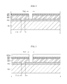
- FIG. 1 is a plan view showing a solar cell panel according to the embodiment
- FIG. 2 is a sectional view taken along line A-A′ of FIG. 1 ;
- FIGS. 3 to 10 are sectional views showing a method of fabricating a solar cell panel according to the embodiment.
- FIG. 1 is a plan view showing a solar cell panel according to the embodiment
- FIG. 2 is a sectional view taken along line A-A′ of FIG. 1 .
- the solar cell panel includes a support substrate 100 , a back electrode layer 200 , a light absorbing layer 300 , a buffer layer 400 , a high-resistance buffer layer 500 , a window layer 600 and a plurality of connection parts 700 .
- the support substrate 10 has a plate shape and supports the back electrode layer 200 , the light absorbing layer 300 , the buffer layer 400 , the high-resistance layer 500 , the window layer 600 and the connection parts 700 .
- the support substrate 100 may be an insulator.
- the support substrate 100 may be a glass substrate, a plastic substrate or a metallic substrate.
- the support substrate 100 may be a soda lime glass substrate.
- the support substrate 100 may be transparent.
- the support substrate 100 may be flexible or rigid.
- the back electrode layer 200 is provided on the support substrate 100 .
- the back electrode layer 200 is a conductive layer.
- the back electrode layer 200 may include a metal, such as molybdenum (Mo).
- the back electrode layer 200 may include at least two layers.
- the layers may be formed by using the same metal or different metals.
- First through holes TH 1 are formed in the back electrode layer 200 .
- the first through holes TH 1 serve as an open region to expose the top surface of the support substrate 100 . When viewed from the top, the first through holes TH 1 extend in the first direction.
- the first through holes TH 1 may have a width in the range of about 80 ⁇ m to about 200 ⁇ m.
- the back electrode layer 200 is divided into a plurality of back electrodes by the first through holes TH 1 . That is, the back electrodes are defined by the first through TH 1 .
- the back electrodes are spaced apart from each other by the first through holes TH 1 .
- the back electrodes are arranged in the form of a stripe.
- the back electrodes can be arranged in the form of a matrix.
- the first through holes TH 1 can be arranged in the form of a lattice.
- the light absorbing layer 300 is disposed on the back electrode layer 200 .
- materials included in the light absorbing layer 300 are filled in the first through holes TH 1 .
- the light absorbing layer 300 may include group I-III-VI compounds.
- the light absorbing layer 300 may include the Cu(In,Ga)Se 2 (CIGS) crystal structure, the Cu(In)Se 2 crystal structure, or the Cu(Ga)Se 2 crystal structure.
- the light absorbing layer 300 has an energy bandgap in the range of about 1 eV to about 1.8 eV.
- the buffer layer 400 is disposed on the light absorbing layer 300 .
- the buffer layer 400 may include CdS and have an energy bandgap in the range of about 2.2 eV to 2.4 eV.
- the high-resistance buffer layer 500 is disposed on the buffer layer 400 .
- the high-resistance buffer layer 500 may include i-ZnO, which is not doped with impurities.
- the high-resistance buffer layer 500 may have an energy bandgap in the range of about 3.1 eV to about 3.3 eV.
- Second through holes TH 2 are formed in the light absorbing layer 300 , the buffer layer 400 and the high-resistance buffer layer 500 .
- the second through holes TH 2 are formed through the light absorbing layer 300 .
- the second through holes TH 2 serve as an open region to expose the top surface of the back electrode layer 200 .
- the second through holes TH 2 are adjacent to the first through holes TH 1 . That is, when viewed from the top, a part of the second through holes TH 2 is located besides the first through holes TH 1 .
- the second through holes TH 2 extend in the first direction.
- the second through holes TH 2 may have a width in the range of about 80 ⁇ m to about 200 ⁇ m.
- Third through holes TH 3 are formed in the light absorbing layer 300 , and the buffer layer 400 .
- the third through holes TH 3 are formed through the light absorbing layer 300 and the buffer layer 400 .
- the third through holes TH 3 serve as an open region to expose the top surface of the back electrode layer 200 .
- the third through holes TH 3 are adjacent to the second through holes TH 2 , respectively. That is, the second through holes TH 2 are interposed between the first through holes TH 1 and the third through holes TH 3 , respectively.
- the third through holes TH 3 extend in the first direction.
- the third through holes TH 3 may have a width in the range of about 30 ⁇ m to about 100 ⁇ m. Inner surfaces of the third through holes TH 3 may be inclined or perpendicular to the top surface of the light absorbing layer 300 .
- a plurality of light absorbing parts may be defined in the light absorbing layer 300 by the second and third through holes TH 2 and TH 3 . That is, the light absorbing layer 300 is divided into the light absorbing parts by the second and third through holes TH 2 and TH 3 .
- a plurality of buffers may be defined in the buffer layer 400 by the second and third through holes TH 2 and TH 3 . That is, the buffer layer 400 is divided into the buffers by the second and third through holes TH 2 and TH 3 .
- the window layer 600 is formed on the high-resistance buffer layer 500 .
- the window layer 600 is a transparent conductive layer.
- the window layer 600 has resistance higher than that of the back electrode layer 200 .
- the window layer 600 may include oxide.
- the window layer 600 may include Al-doped zinc oxide (AZO) or Ga-doped zinc oxide (GZO).
- AZO Al-doped zinc oxide
- GZO Ga-doped zinc oxide
- Fourth through holes TH 4 are formed in the high-resistance buffer layer 500 and the window layer 600 .
- the fourth through holes TH 4 are formed through the high-resistance buffer layer 500 and the window layer 600 .
- the fourth through holes TH 4 are adjacent to the second through holes TH 2 , respectively.
- the fourth through holes TH 4 are disposed next to the second through holes TH 2 , respectively.
- the fourth through holes TH 4 are disposed next to the second through holes TH 2 in parallel to the second through holes TH 2 , respectively.
- the fourth through holes TH 4 extend in the first direction.
- the fourth through holes TH 4 may correspond to the third through holes TH 3 , respectively.
- the fourth through holes TH 4 are connected to the third through holes TH 3 , respectively.
- the fourth through holes TH 4 may overlap with the third through holes TH 3 , respectively.
- the fourth through holes TH 4 may have a width W 4 larger than that of the third through holes TH 3 .
- the fourth through holes TH 4 may have the width W 4 in the range of about 80 ⁇ m to about 120 ⁇ m.
- the inner surfaces 601 of the fourth through holes TH 4 may be inclined with respect to the top surface of the window layer 600 .
- the inner surfaces 601 of the fourth through holes TH 4 may be inclined at an angle of about 0° to about 30° with respect to the plane perpendicular to the top surface of the window layer 600 .
- a plurality of high-resistance buffers may be defined in the high-resistance buffer layer 500 by the second and fourth through holes TH 2 and TH 4 . That is, the high-resistance buffer layer 500 is divided into the high-resistance buffers by the second and fourth through holes TH 2 and TH 4 .
- the window layer 600 is divided into a plurality of windows by the fourth through hole TH 4 . That is, the windows are defined by the fourth through hole TH 4 .
- the windows may have shape corresponding to the shape of the back electrodes. That is, the windows are arranged in the form of a stripe. In addition, the windows can be arranged in the form of a matrix.
- a plurality of cells C 1 , C 2 . . . and Cn are defined by the third and fourth through holes TH 3 and TH 4 .
- the cells C 1 , C 2 . . . and Cn are defined by the second, third and fourth through holes TH 2 , TH 3 and TH 4 . That is, the solar cell apparatus according to the embodiment may be divided into the cells C 1 , C 2 . . . and Cn by the second, third and fourth through holes TH 2 , TH 3 and TH 4 .
- the cells C 1 , C 2 . . . and Cn are connected with each other in the second direction crossing the first direction. That is, current may flow in the second direction through the cells C 1 , C 2 . . . and Cn.
- Each of the cells C 1 , C 2 . . . and Cn may include the back electrode, the light absorbing part, the buffer, the high-resistance buffer and the window.
- each of the cells C 1 , C 2 . . . and Cn may have a stack structure of the back electrode, the light absorbing part, the buffer, the high-resistance buffer and the window. At this time, a step difference is formed between the window and the light absorbing part.
- the second cell C 2 may include the back electrode 210 , the light absorbing part 310 , the buffer 410 , the high-resistance buffer 510 and the window 610 .
- the window 610 is formed on the light absorbing part 310 .
- a step difference is formed between the window 610 and the light absorbing part 310 .
- a lateral side 311 of the light absorbing part 310 protrudes in the lateral direction more than the lateral side 611 of the window 610 . That is, the lateral side 311 of the light absorbing part 310 may be disposed in the plane different from the plane of the lateral side 611 of the window 610 . At this time, the lateral side 611 of the window 610 may be inclined with respect to the top surface of the back electrode layer 200 .
- the lateral side 311 of the light absorbing part 310 may be an inner surface of the third through hole TH 3 .
- the lateral side 611 of the window 610 may be an inner surface of the fourth through hole TH 4 .
- a step difference may be formed between the high-resistance buffer 510 and the buffer 410 .
- the buffer 410 may have a planar shape corresponding to the light absorbing part 310 .
- one outer peripheral portion of the high-resistance buffer 510 may match with one outer peripheral portion of the window 610 .
- connection parts 700 are disposed in the second through holes TH 2 .
- the connection parts 700 extend downward from the window layer 600 and are connected to the back electrode layer 200 .
- the connection parts 700 extend from the window of the first cell C 1 and are connected to the back electrode of the second cell C 2 .
- connection parts 700 connect adjacent cells with each other.
- the connection parts 700 connect windows with the back electrodes included in adjacent cells C 1 , C 2 . . . and Cn.
- connection parts 700 are integrally formed with the window layer 600 . That is, the material used to form the connection parts 700 may be equal to the material used to form the window layer 600 .
- the solar cell panel according to the embodiment includes the third through holes TH 3 having the relatively small width W 1 and the fourth through holes TH 4 having the relatively large width W 2 .
- the fourth through holes TH 4 divide the window layer 600 having the relatively low resistance and the third through holes TH 3 divide the light absorbing layer 300 having the relatively high resistance.
- the third and fourth through holes TH 3 and TH 4 can effectively divide the light absorbing layer 300 and the window layer 600 , respectively.
- the third and fourth through holes TH 3 and TH 4 can divide the cells C 1 , C 2 . . . and Cn such that the short between adjacent cells can be effectively prevented.
- the step difference SC is formed between the light absorbing layer 300 and the window layer 600 . That is, the window layer 600 is laminated on the light absorbing layer 300 in the form of a stair. Due to the step difference SC, external impurities can be prevented from penetrating into the third through holes TH 3 . That is, the external impurities are blocked by the step difference SC.
- the solar cell panel according to the embodiment can prevent the short between adjacent cells C 1 , C 2 . . . and Cn and can improve the photoelectric efficiency.
- the solar cell panel according to the embodiment can effectively protect a portion of the light absorbing layer 300 , which corresponds to an active layer where the solar light is converted into the electric energy.
- the third through holes TH 3 divide the light absorbing layer 300 having the high resistance, the portion of the light absorbing layer 300 disposed in the active layer with the small width W 1 and the back electrode layer 200 can be effectively protected.
- the solar cell apparatus according to the embodiment may have the improved durability and reliability.
- FIGS. 3 to 10 are sectional views showing the method of fabricating the solar cell apparatus according to the embodiment.
- the description about the method of fabricating the solar cell according to the embodiment will be made with reference to the above description about the solar cell apparatus.
- the above description about the solar cell apparatus will be basically incorporated in the description about the method of fabricating the solar cell.
- the back electrode layer 200 is formed on the support substrate 100 .
- the back electrode layer 200 is patterned to form the first through holes TH 1 .
- a plurality of back electrodes are formed on the support substrate 100 .
- the back electrode layer 200 is patterned by a laser.
- the back electrode layer 200 may include Mo and may have at least two layers formed based on process conditions different from each other.
- the first through holes TH 1 expose the top surface of the support substrate 100 and have a width in the range of about 80 ⁇ m to about 200 ⁇ m.
- an additional layer such as a diffusion barrier layer, may be interposed between the support substrate 100 and the back electrode layer 200 .
- the first through holes TH 1 expose the top surface of the additional layer.
- the light absorbing layer 300 , the buffer layer 400 and the high-resistance buffer layer 500 are formed on the back electrode layer 200 .
- the light absorbing layer 300 can be formed through the sputtering scheme or the evaporation scheme.
- the light absorbing layer 300 may be formed through various schemes such as a scheme of forming a Cu(In,Ga)Se 2 (CIGS) based light absorbing layer 300 by simultaneously or separately evaporating Cu, In, Ga, and Se and a scheme of performing a selenization process after a metallic precursor layer has been formed
- CIGS Cu(In,Ga)Se 2
- the metallic precursor layer is formed on the back electrode layer 200 through a sputtering process employing a Cu target, an In target, or a Ga target.
- the metallic precursor layer is subject to the selenization process so that the Cu (In, Ga) Se 2 (CIGS) based light absorbing layer 300 is formed.
- the sputtering process employing the Cu target, the In target, and the Ga target and the selenization process may be simultaneously performed.
- a CIS or a CIG based light absorbing layer 300 may be formed through the sputtering process employing only Cu and In targets or only Cu and Ga targets and the selenization process.
- CdS is deposited through the sputtering process or the chemical bath deposition (CBD) process to form the buffer layer 400 .
- ZnO is deposited on the buffer layer 400 through the sputtering process to form the high-resistance buffer layer 500 .
- the buffer layer 400 and the high-resistance buffer layer 500 may have the shallow thickness.
- the buffer layer 400 and the high-resistance buffer layer 500 may have the thickness in the range of about 1 nm to about 80 nm.
- the light absorbing layer 300 , the buffer layer 400 and the high-resistance buffer layer 500 are partially removed to form the second through holes TH 2 .
- the second through holes TH 2 can be formed by a mechanical device, such as a tip, or a laser device.
- the light absorbing layer 300 and the buffer layer 400 may be patterned by using the tip having a width in the range of about 40 ⁇ m to about 180 ⁇ m.
- the second through hole TH 2 may have the width in the range of about 100 ⁇ m to about 200 ⁇ m. In addition, the second through hole TH 2 may expose a part of the top surface of the back electrode layer 200 .
- a transparent conductive layer 600 a is formed on the light absorbing layer 300 and in the second through holes TH 2 . That is, the transparent conductive layer 600 a can be formed by depositing transparent conductive materials on the high-resistance buffer layer 500 and in the second through holes TH 2 .
- the transparent conductive layer 600 a can be formed by depositing Al-doped zinc oxide (AZO) on the top surface of the high-resistance buffer layer and in the second through holes TH 2 through the sputtering process.
- AZO Al-doped zinc oxide
- the transparent conductive material is filled in the second through holes TH 2 and the transparent conductive layer 600 a directly makes contact with the back electrode layer 200 .
- a mask pattern 800 is formed on the transparent conductive layer 600 a .
- the mask pattern 800 may include exposure holes 801 to expose the top surface of the transparent conductive layer 600 a .
- the exposure holes 801 are adjacent to the second through holes TH 2 , respectively.
- the exposure holes 801 extend in the first direction.
- the mask pattern 800 includes a first mask part 810 and a second mask part 820 .
- the first mask part 810 is adjacent to the exposure holes 801 . That is, the exposure holes 801 are formed through the first mask part 810 .
- the first mask part 810 has a thickness T 1 thinner than a thickness of the second mask part 820 .
- the first mask part 810 may have the thickness T 1 in the range of about 20 ⁇ m to about 40 ⁇ m.
- the second mask part 820 has a thickness T 2 thicker than the thickness T 1 of the first mask part 810 .
- the second mask part 820 may have the thickness T 2 in the range of about 50 ⁇ m to about 90 ⁇ m.
- a material used to form the mask pattern 800 may include a photoresist film.
- the light absorbing layer 300 , the buffer layer 400 , the high-resistance buffer layer 500 , and the transparent conductive layer are etched by using the mask pattern 800 as an etching mask.
- the mask pattern 800 as an etching mask.
- a plurality of third through holes TH 3 are formed in the light absorbing layer 300 and the buffer layer 400 .
- the third through holes TH 3 may correspond to the exposure holes 801 , respectively.
- the third through holes TH 3 match with the exposure holes 801 , respectively.
- a wet etching process or a dry etching process may be performed to form the third through holes TH 3 .
- etching solutions can be used to form the third through holes TH 3 through the wet etching process.
- various etching gases can be used to form the third through holes TH 3 through the dry etching process.
- the first mask part 810 is removed and the thickness of the second mask part 820 is reduced.
- O 2 plasma may be sprayed toward the mask pattern 800 in order to remove the first mask part 810 .
- the high-resistance buffer layer 500 and the window layer 600 are patterned by using a mask pattern 821 where the first mask part 810 has been removed.
- the fourth through holes TH 4 are formed in the high-resistance buffer layer 500 and the window layer 600 .
- the fourth through holes TH 4 can be formed by selectively etching the high-resistance buffer layer 500 and the window layer 600 using the etching solution.
- the fourth through holes TH 4 can be formed corresponding to the region where the first mask part 810 has been removed.
- the mask pattern 821 is removed, so that the solar cell panel capable of preventing the short and improving the reliability and the durability can be obtained.
- the solar cell panel according to the embodiment corresponds to the solar cell apparatus that receives solar light to convert the solar light into the electric energy.
- the embodiment may be applied to the solar cell apparatus as well as the solar cell panel.
- the solar cell apparatus according to the embodiment can be applied in the field of solar light generation.
Landscapes
- Photovoltaic Devices (AREA)
Applications Claiming Priority (3)
| Application Number | Priority Date | Filing Date | Title |
|---|---|---|---|
| KR1020100089133A KR101262455B1 (ko) | 2010-09-10 | 2010-09-10 | 태양광 발전장치 및 이의 제조방법 |
| KR10-2010-0089133 | 2010-09-10 | ||
| PCT/KR2011/003120 WO2012033274A1 (ko) | 2010-09-10 | 2011-04-27 | 태양광 발전장치 및 이의 제조방법 |
Publications (2)
| Publication Number | Publication Date |
|---|---|
| US20130037099A1 US20130037099A1 (en) | 2013-02-14 |
| US9818897B2 true US9818897B2 (en) | 2017-11-14 |
Family
ID=45810845
Family Applications (1)
| Application Number | Title | Priority Date | Filing Date |
|---|---|---|---|
| US13/639,704 Active 2033-08-01 US9818897B2 (en) | 2010-09-10 | 2011-04-27 | Device for generating solar power and method for manufacturing same |
Country Status (6)
| Country | Link |
|---|---|
| US (1) | US9818897B2 (enExample) |
| EP (1) | EP2538454A1 (enExample) |
| JP (1) | JP2013537364A (enExample) |
| KR (1) | KR101262455B1 (enExample) |
| CN (1) | CN103081123A (enExample) |
| WO (1) | WO2012033274A1 (enExample) |
Cited By (1)
| Publication number | Priority date | Publication date | Assignee | Title |
|---|---|---|---|---|
| US20170373262A1 (en) * | 2014-12-23 | 2017-12-28 | Stichting Energieonderzoek Centrum Nederland | Method of making a current collecting grid for solar cells |
Families Citing this family (7)
| Publication number | Priority date | Publication date | Assignee | Title |
|---|---|---|---|---|
| US20090293955A1 (en) * | 2007-11-07 | 2009-12-03 | Qualcomm Incorporated | Photovoltaics with interferometric masks |
| US20100096006A1 (en) * | 2008-10-16 | 2010-04-22 | Qualcomm Mems Technologies, Inc. | Monolithic imod color enhanced photovoltaic cell |
| KR20140142416A (ko) * | 2013-06-03 | 2014-12-12 | 삼성에스디아이 주식회사 | 태양 전지 및 이의 제조 방법 |
| KR102042026B1 (ko) * | 2013-06-20 | 2019-11-27 | 엘지이노텍 주식회사 | 태양전지 |
| KR20150041929A (ko) * | 2013-10-10 | 2015-04-20 | 엘지이노텍 주식회사 | 태양광 발전장치 |
| CN108183088B (zh) * | 2017-12-27 | 2020-06-12 | 武汉华星光电技术有限公司 | 一种膜层套孔及阵列基板制备方法 |
| JP2022085070A (ja) * | 2020-11-27 | 2022-06-08 | 株式会社リコー | 光電変換モジュール、電子機器、及び電源モジュール |
Citations (14)
| Publication number | Priority date | Publication date | Assignee | Title |
|---|---|---|---|---|
| US5538902A (en) * | 1993-06-29 | 1996-07-23 | Sanyo Electric Co., Ltd. | Method of fabricating a photovoltaic device having a three-dimensional shape |
| US6455347B1 (en) * | 1999-06-14 | 2002-09-24 | Kaneka Corporation | Method of fabricating thin-film photovoltaic module |
| US20050056312A1 (en) * | 2003-03-14 | 2005-03-17 | Young David L. | Bifacial structure for tandem solar cells |
| KR20070047787A (ko) | 2004-08-13 | 2007-05-07 | 쓰리엠 이노베이티브 프로퍼티즈 캄파니 | 성형 전면 팻치 |
| US20070193622A1 (en) | 2004-03-31 | 2007-08-23 | Hironobu Sai | Laminate Type Thin-Film Solar Cell And Method For Manufacturing The Same |
| US20070209700A1 (en) * | 2004-04-28 | 2007-09-13 | Honda Motor Co., Ltd. | Chalcopyrite Type Solar Cell |
| US20080110491A1 (en) * | 2006-03-18 | 2008-05-15 | Solyndra, Inc., | Monolithic integration of non-planar solar cells |
| JP2008140920A (ja) | 2006-11-30 | 2008-06-19 | Sanyo Electric Co Ltd | 太陽電池モジュール及び太陽電池モジュールの製造方法 |
| US20090084425A1 (en) * | 2007-09-28 | 2009-04-02 | Erel Milshtein | Scribing Methods for Photovoltaic Modules Including a Mechanical Scribe |
| WO2009150654A2 (en) | 2008-06-12 | 2009-12-17 | Yissum Research Development Company | Solar volumetric structure |
| WO2010044738A1 (en) * | 2008-10-13 | 2010-04-22 | Solibro Research Ab | A method for manufacturing a thin film solar cell module |
| JP2010177463A (ja) * | 2009-01-29 | 2010-08-12 | Mitsubishi Electric Corp | 薄膜太陽電池およびその製造方法並びに溝形成装置 |
| KR20100112826A (ko) | 2009-04-10 | 2010-10-20 | 주성엔지니어링(주) | 박막형 태양전지의 제조방법 및 제조장치 |
| KR20110001808A (ko) | 2009-06-30 | 2011-01-06 | 엘지이노텍 주식회사 | 태양전지 및 이의 제조방법 |
Family Cites Families (3)
| Publication number | Priority date | Publication date | Assignee | Title |
|---|---|---|---|---|
| JP2009135337A (ja) * | 2007-11-30 | 2009-06-18 | Showa Shell Sekiyu Kk | Cis系太陽電池の積層構造、cis系薄膜太陽電池の集積構造及び製造方法 |
| KR101460580B1 (ko) * | 2008-02-20 | 2014-11-12 | 주성엔지니어링(주) | 박막형 태양전지 및 그 제조방법 |
| KR20100030944A (ko) * | 2008-09-11 | 2010-03-19 | 엘지이노텍 주식회사 | 태양전지의 제조방법 |
-
2010
- 2010-09-10 KR KR1020100089133A patent/KR101262455B1/ko not_active Expired - Fee Related
-
2011
- 2011-04-27 WO PCT/KR2011/003120 patent/WO2012033274A1/ko not_active Ceased
- 2011-04-27 EP EP11823707A patent/EP2538454A1/en not_active Withdrawn
- 2011-04-27 CN CN2011800412097A patent/CN103081123A/zh active Pending
- 2011-04-27 US US13/639,704 patent/US9818897B2/en active Active
- 2011-04-27 JP JP2013528101A patent/JP2013537364A/ja not_active Withdrawn
Patent Citations (15)
| Publication number | Priority date | Publication date | Assignee | Title |
|---|---|---|---|---|
| US5538902A (en) * | 1993-06-29 | 1996-07-23 | Sanyo Electric Co., Ltd. | Method of fabricating a photovoltaic device having a three-dimensional shape |
| US6455347B1 (en) * | 1999-06-14 | 2002-09-24 | Kaneka Corporation | Method of fabricating thin-film photovoltaic module |
| US20050056312A1 (en) * | 2003-03-14 | 2005-03-17 | Young David L. | Bifacial structure for tandem solar cells |
| US20070193622A1 (en) | 2004-03-31 | 2007-08-23 | Hironobu Sai | Laminate Type Thin-Film Solar Cell And Method For Manufacturing The Same |
| US20070209700A1 (en) * | 2004-04-28 | 2007-09-13 | Honda Motor Co., Ltd. | Chalcopyrite Type Solar Cell |
| KR20070047787A (ko) | 2004-08-13 | 2007-05-07 | 쓰리엠 이노베이티브 프로퍼티즈 캄파니 | 성형 전면 팻치 |
| US20080110491A1 (en) * | 2006-03-18 | 2008-05-15 | Solyndra, Inc., | Monolithic integration of non-planar solar cells |
| JP2008140920A (ja) | 2006-11-30 | 2008-06-19 | Sanyo Electric Co Ltd | 太陽電池モジュール及び太陽電池モジュールの製造方法 |
| US20100065115A1 (en) | 2006-11-30 | 2010-03-18 | Sanyo Electric Co., Ltd. | Solar cell module and solar cell module manufacturing method |
| US20090084425A1 (en) * | 2007-09-28 | 2009-04-02 | Erel Milshtein | Scribing Methods for Photovoltaic Modules Including a Mechanical Scribe |
| WO2009150654A2 (en) | 2008-06-12 | 2009-12-17 | Yissum Research Development Company | Solar volumetric structure |
| WO2010044738A1 (en) * | 2008-10-13 | 2010-04-22 | Solibro Research Ab | A method for manufacturing a thin film solar cell module |
| JP2010177463A (ja) * | 2009-01-29 | 2010-08-12 | Mitsubishi Electric Corp | 薄膜太陽電池およびその製造方法並びに溝形成装置 |
| KR20100112826A (ko) | 2009-04-10 | 2010-10-20 | 주성엔지니어링(주) | 박막형 태양전지의 제조방법 및 제조장치 |
| KR20110001808A (ko) | 2009-06-30 | 2011-01-06 | 엘지이노텍 주식회사 | 태양전지 및 이의 제조방법 |
Non-Patent Citations (4)
| Title |
|---|
| English machine translation of Suehiro et al. (JP 2010-177463) published on Aug. 12, 2010. * |
| International Search Report in International Application No. PCT/KR2011/003120, filed Apr. 27, 2011. |
| Notice of Allowance dated Feb. 13, 2013 in Korean Application No. 10-2010-0089133, filed Sep. 10, 2010. |
| Office Action dated Nov. 28, 2011 in Korean Application No. 10-2010-0089133, filed Sep. 10, 2010. |
Cited By (2)
| Publication number | Priority date | Publication date | Assignee | Title |
|---|---|---|---|---|
| US20170373262A1 (en) * | 2014-12-23 | 2017-12-28 | Stichting Energieonderzoek Centrum Nederland | Method of making a current collecting grid for solar cells |
| US11581502B2 (en) * | 2014-12-23 | 2023-02-14 | Nederlandse Organisatie Voortoegepast-Natuurwetenschappelijk Onderzoek Tno | Method of making a current collecting grid for solar cells |
Also Published As
| Publication number | Publication date |
|---|---|
| US20130037099A1 (en) | 2013-02-14 |
| JP2013537364A (ja) | 2013-09-30 |
| EP2538454A1 (en) | 2012-12-26 |
| KR20120026925A (ko) | 2012-03-20 |
| KR101262455B1 (ko) | 2013-05-08 |
| CN103081123A (zh) | 2013-05-01 |
| WO2012033274A1 (ko) | 2012-03-15 |
Similar Documents
| Publication | Publication Date | Title |
|---|---|---|
| KR101210168B1 (ko) | 태양광 발전장치 및 이의 제조방법 | |
| US9818897B2 (en) | Device for generating solar power and method for manufacturing same | |
| CN102449780B (zh) | 太阳能电池装置及其制造方法 | |
| US20120273039A1 (en) | Solar Cell Apparatus and Method for Manufacturing the Same | |
| KR100999797B1 (ko) | 태양광 발전장치 및 이의 제조방법 | |
| US8779282B2 (en) | Solar cell apparatus and method for manufacturing the same | |
| US20130133740A1 (en) | Photovoltaic device and method for manufacturing same | |
| KR101114079B1 (ko) | 태양광 발전장치 및 이의 제조방법 | |
| US9954122B2 (en) | Solar cell apparatus and method of fabricating the same | |
| CN106876510A (zh) | 太阳能电池装置 | |
| KR101349429B1 (ko) | 태양광 발전장치 | |
| KR101055019B1 (ko) | 태양광 발전장치 및 이의 제조방법 | |
| US20130019943A1 (en) | Solar power generating device, and method for manufacturing same | |
| KR101144447B1 (ko) | 태양광 발전장치 및 이의 제조방법 | |
| KR101210104B1 (ko) | 태양광 발전장치 | |
| KR101081222B1 (ko) | 태양광 발전장치 | |
| KR20140047258A (ko) | 태양전지 및 이의 제조 방법 | |
| KR20120129108A (ko) | 태양광 발전장치 및 이의 제조방법 |
Legal Events
| Date | Code | Title | Description |
|---|---|---|---|
| AS | Assignment |
Owner name: LG INNOTEK CO., LTD., KOREA, REPUBLIC OF Free format text: ASSIGNMENT OF ASSIGNORS INTEREST;ASSIGNOR:LEE, JIN WOO;REEL/FRAME:029088/0622 Effective date: 20120927 |
|
| STCF | Information on status: patent grant |
Free format text: PATENTED CASE |
|
| MAFP | Maintenance fee payment |
Free format text: PAYMENT OF MAINTENANCE FEE, 4TH YEAR, LARGE ENTITY (ORIGINAL EVENT CODE: M1551); ENTITY STATUS OF PATENT OWNER: LARGE ENTITY Year of fee payment: 4 |
|
| MAFP | Maintenance fee payment |
Free format text: PAYMENT OF MAINTENANCE FEE, 8TH YEAR, LARGE ENTITY (ORIGINAL EVENT CODE: M1552); ENTITY STATUS OF PATENT OWNER: LARGE ENTITY Year of fee payment: 8 |