US9818641B1 - Apparatus and method of forming self-aligned cuts in mandrel and a non-mandrel lines of an array of metal lines - Google Patents
Apparatus and method of forming self-aligned cuts in mandrel and a non-mandrel lines of an array of metal lines Download PDFInfo
- Publication number
- US9818641B1 US9818641B1 US15/271,497 US201615271497A US9818641B1 US 9818641 B1 US9818641 B1 US 9818641B1 US 201615271497 A US201615271497 A US 201615271497A US 9818641 B1 US9818641 B1 US 9818641B1
- Authority
- US
- United States
- Prior art keywords
- mandrel
- trench
- cuts
- hardmask layer
- beta
- Prior art date
- Legal status (The legal status is an assumption and is not a legal conclusion. Google has not performed a legal analysis and makes no representation as to the accuracy of the status listed.)
- Expired - Fee Related
Links
Images


Classifications
-
- H—ELECTRICITY
- H01—ELECTRIC ELEMENTS
- H01L—SEMICONDUCTOR DEVICES NOT COVERED BY CLASS H10
- H01L21/00—Processes or apparatus adapted for the manufacture or treatment of semiconductor or solid state devices or of parts thereof
- H01L21/67—Apparatus specially adapted for handling semiconductor or electric solid state devices during manufacture or treatment thereof; Apparatus specially adapted for handling wafers during manufacture or treatment of semiconductor or electric solid state devices or components ; Apparatus not specifically provided for elsewhere
- H01L21/67005—Apparatus not specifically provided for elsewhere
- H01L21/67011—Apparatus for manufacture or treatment
- H01L21/67138—Apparatus for wiring semiconductor or solid state device
-
- H—ELECTRICITY
- H01—ELECTRIC ELEMENTS
- H01L—SEMICONDUCTOR DEVICES NOT COVERED BY CLASS H10
- H01L21/00—Processes or apparatus adapted for the manufacture or treatment of semiconductor or solid state devices or of parts thereof
- H01L21/70—Manufacture or treatment of devices consisting of a plurality of solid state components formed in or on a common substrate or of parts thereof; Manufacture of integrated circuit devices or of parts thereof
- H01L21/71—Manufacture of specific parts of devices defined in group H01L21/70
- H01L21/768—Applying interconnections to be used for carrying current between separate components within a device comprising conductors and dielectrics
- H01L21/76801—Applying interconnections to be used for carrying current between separate components within a device comprising conductors and dielectrics characterised by the formation and the after-treatment of the dielectrics, e.g. smoothing
- H01L21/76802—Applying interconnections to be used for carrying current between separate components within a device comprising conductors and dielectrics characterised by the formation and the after-treatment of the dielectrics, e.g. smoothing by forming openings in dielectrics
- H01L21/76816—Aspects relating to the layout of the pattern or to the size of vias or trenches
-
- H—ELECTRICITY
- H01—ELECTRIC ELEMENTS
- H01L—SEMICONDUCTOR DEVICES NOT COVERED BY CLASS H10
- H01L21/00—Processes or apparatus adapted for the manufacture or treatment of semiconductor or solid state devices or of parts thereof
- H01L21/02—Manufacture or treatment of semiconductor devices or of parts thereof
- H01L21/04—Manufacture or treatment of semiconductor devices or of parts thereof the devices having at least one potential-jump barrier or surface barrier, e.g. PN junction, depletion layer or carrier concentration layer
- H01L21/18—Manufacture or treatment of semiconductor devices or of parts thereof the devices having at least one potential-jump barrier or surface barrier, e.g. PN junction, depletion layer or carrier concentration layer the devices having semiconductor bodies comprising elements of Group IV of the Periodic System or AIIIBV compounds with or without impurities, e.g. doping materials
- H01L21/30—Treatment of semiconductor bodies using processes or apparatus not provided for in groups H01L21/20 - H01L21/26
- H01L21/31—Treatment of semiconductor bodies using processes or apparatus not provided for in groups H01L21/20 - H01L21/26 to form insulating layers thereon, e.g. for masking or by using photolithographic techniques; After treatment of these layers; Selection of materials for these layers
- H01L21/3105—After-treatment
- H01L21/311—Etching the insulating layers by chemical or physical means
- H01L21/31144—Etching the insulating layers by chemical or physical means using masks
-
- H—ELECTRICITY
- H01—ELECTRIC ELEMENTS
- H01L—SEMICONDUCTOR DEVICES NOT COVERED BY CLASS H10
- H01L21/00—Processes or apparatus adapted for the manufacture or treatment of semiconductor or solid state devices or of parts thereof
- H01L21/67—Apparatus specially adapted for handling semiconductor or electric solid state devices during manufacture or treatment thereof; Apparatus specially adapted for handling wafers during manufacture or treatment of semiconductor or electric solid state devices or components ; Apparatus not specifically provided for elsewhere
- H01L21/68—Apparatus specially adapted for handling semiconductor or electric solid state devices during manufacture or treatment thereof; Apparatus specially adapted for handling wafers during manufacture or treatment of semiconductor or electric solid state devices or components ; Apparatus not specifically provided for elsewhere for positioning, orientation or alignment
- H01L21/682—Mask-wafer alignment
-
- H—ELECTRICITY
- H01—ELECTRIC ELEMENTS
- H01L—SEMICONDUCTOR DEVICES NOT COVERED BY CLASS H10
- H01L21/00—Processes or apparatus adapted for the manufacture or treatment of semiconductor or solid state devices or of parts thereof
- H01L21/70—Manufacture or treatment of devices consisting of a plurality of solid state components formed in or on a common substrate or of parts thereof; Manufacture of integrated circuit devices or of parts thereof
- H01L21/71—Manufacture of specific parts of devices defined in group H01L21/70
- H01L21/768—Applying interconnections to be used for carrying current between separate components within a device comprising conductors and dielectrics
- H01L21/76897—Formation of self-aligned vias or contact plugs, i.e. involving a lithographically uncritical step
-
- H—ELECTRICITY
- H01—ELECTRIC ELEMENTS
- H01L—SEMICONDUCTOR DEVICES NOT COVERED BY CLASS H10
- H01L23/00—Details of semiconductor or other solid state devices
- H01L23/52—Arrangements for conducting electric current within the device in operation from one component to another, i.e. interconnections, e.g. wires, lead frames
- H01L23/522—Arrangements for conducting electric current within the device in operation from one component to another, i.e. interconnections, e.g. wires, lead frames including external interconnections consisting of a multilayer structure of conductive and insulating layers inseparably formed on the semiconductor body
- H01L23/528—Geometry or layout of the interconnection structure
-
- H01L27/11—
-
- H—ELECTRICITY
- H10—SEMICONDUCTOR DEVICES; ELECTRIC SOLID-STATE DEVICES NOT OTHERWISE PROVIDED FOR
- H10B—ELECTRONIC MEMORY DEVICES
- H10B10/00—Static random access memory [SRAM] devices
Definitions
- the present invention relates to semiconductor devices and methods of making the same. More specifically, the invention relates to methods of making multiple closely located cuts on a single metal line of an integrated circuit through the use of a single cut mask.
- SADP Self-aligned double patterning
- Such SADP techniques typically involve the use of a lithographic mask (designated herein as a “mandrel mask”) to pattern and print an array of longitudinally extending parallel mandrels onto a top surface of a hardmask layer.
- the longitudinal direction of the mandrels defines the Y direction of the array.
- Spacers are then formed on both sidewalls of each mandrel.
- the spacers are considered to be self-aligned in the X direction (perpendicular to the Y direction) because the spacing between the spacers in the X direction was defined by the sidewalls of the existing mandrels.
- each combination of mandrel and associated spacer pair is separated by exposed parallel portions of the hardmask layer, which are absent any overlaying mandrels or spacers.
- the mandrels are patterned down into a dielectric layer of the integrated circuit to form mandrel metal lines.
- the exposed portions of the hardmask layer are also patterned down into the dielectric layer to form non-mandrel metal lines. Therefore, each array of parallel metal lines in an interconnection system formed using an SADP process will include alternating mandrel and non-mandrel metal lines, which are separated by a distance equal to the width of the self-aligned spacers.
- a plurality of cuts must be lithographically patterned into the mandrel and non-mandrel metal lines of an array at specific locations to direct current flow between the dielectric layers and the devices.
- another lithographic mask (designated herein as a “mandrel line cut mask”) is used to pattern such mandrel cuts into the mandrel metal lines.
- non-mandrel line cut mask is used to pattern such non-mandrel cuts into the non-mandrel metal lines.
- a typical SADP process for patterning arrays of metal lines in a complex interconnection system for an integrated circuit requires at least three masks: a mandrel mask, a mandrel line cut mask, and a non-mandrel line cut mask.
- Development and use of such masks requires complex, state of the art technology, especially when lithographically printing aggressively small features in such technology class sizes as the 14 nanometer (nm) class and beyond. Therefore it is desirable to keep the number of masks to a minimum due to the large costs associated with the development and use of such masks.
- the present invention offers advantages and alternatives over the prior art by providing an apparatus and method of forming pairs of cuts in a mandrel or non-mandrel metal line, or both, for an integrated circuit.
- the metal lines extend longitudinally in a Y direction and are self-aligned in a perpendicular X direction.
- the cuts of a pair of cuts are formed closer than 100 nm apart in the Y direction on any single metal line through the use of a single mandrel line cut mask and/or a single non-mandrel line cut mask. Additionally the cuts of any pair of cuts on any single metal line are self-aligned in the Y direction.
- a method in accordance with one or more aspects of the present invention includes providing a structure having a first hardmask layer, second hardmask layer, third hardmask layer and mandrel layer disposed respectively over a dielectric stack.
- An array of mandrels is then patterned into the mandrel layer.
- a beta trench is patterned into the mandrels.
- a gamma trench is patterned into the second hardmask layer.
- Self-aligned first inner spacers are formed on sidewalls of the beta trench.
- Self-aligned second inner spaces are formed on sidewalls of the gamma trench. The first and second inner spaces form a portion of a pattern.
- the pattern is etched into the dielectric stack to form an array of alternating mandrel and non-mandrel metal lines extending longitudinally in a Y direction and being self-aligned in a perpendicular X direction.
- the portion of the pattern formed by the first and second inner spaces forms a first pair of mandrel line cuts in a mandrel line and a second pair of non-mandrel line cuts in a non-mandrel line respectively.
- the first and second pair of line cuts are self-aligned in the Y direction.
- the method includes providing a structure having a first hardmask layer, second hardmask layer, third hardmask layer and mandrel layer disposed respectively over a dielectric stack.
- An array of mandrels is patterned into the mandrel layer.
- One of a gamma trench into the mandrels and a beta trench into the second hardmask layer is then patterned.
- Self-aligned first inner spacers are formed on sidewalls of the one of the gamma trench and the beta trench. The first inner spacers form a portion of a pattern.
- the pattern is etched into the dielectric stack to form an array of alternating mandrel and non-mandrel metal lines extending longitudinally in a Y direction and being self-aligned in a perpendicular X direction.
- the portion of the pattern formed by the first inner spacers forms a first pair of line cuts in one of a mandrel line and a non-mandrel line.
- the cuts in the first pair of line cuts are separated by a center-to-center distance of less than 100 nm and are self-aligned in the Y direction.
- a structure for an integrated circuit in another aspect of the present invention, includes a dielectric layer.
- An array of metal lines is disposed in the dielectric layer.
- the array includes alternating parallel mandrel and non-mandrel metal lines extending longitudinally in a Y direction and being self-aligned in a perpendicular X direction.
- the array also includes one of a pair of mandrel line cuts disposed in a mandrel line of the array and a pair of non-mandrel line cuts disposed in a non-mandrel line of the array.
- the cuts in the one of the pair of mandrel line cuts and the pair of non-mandrel line cuts are separated by a center-to center distance of less than 100 nm and are self-aligned in the Y direction.
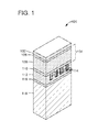
- FIG. 1 is simplified perspective view of an exemplary embodiment of a structure for an integrated circuit device at an intermediate stage of manufacturing having a first hardmask layer disposed over a dielectric stack in accordance with the present invention
- FIG. 2 is a perspective view of an exemplary embodiment of the structure of FIG. 1 having a mandrel layer and a second hardmask layer and a third hardmask layer disposed respectively on the first hardmask layer in accordance with the present invention
- FIG. 3 is perspective view of an exemplary embodiment of the structure of FIG. 2 having a first mandrel lithographic stack with mandrels patterned thereon in accordance with the present invention
- FIG. 4 is a perspective view of an exemplary embodiment of the structure of FIG. 3 having the mandrels patterned into the mandrel layer;
- FIG. 5 is a perspective view of an exemplary embodiment of the structure of FIG. 4 having the mandrels patterned into the third hardmask layer;
- FIG. 6 is a perspective view of an exemplary embodiment of the structure of FIG. 5 having a second beta lithographic stack with a beta opening patterned therein in accordance with the present invention
- FIG. 7A is a perspective view of an exemplary embodiment of the structure of FIG. 6 having a beta trench in a mandrel in accordance with the present invention
- FIG. 7B is a perspective top view of FIG. 7A ;
- FIG. 8 is a perspective view of an exemplary embodiment of the structure of FIG. 7A having a third gamma lithographic stack with a gamma opening patterned therein in accordance with the present invention
- FIG. 9A is a perspective view of an exemplary embodiment of the structure of FIG. 8 having a gamma trench in the second hardmask layer in accordance with the present invention.
- FIG. 9B is a perspective top view of FIG. 9A ;
- FIG. 10 is a perspective view of the structure of FIG. 9A having a spacer layer disposed thereon in accordance with the present invention.
- FIG. 11A is a perspective view of the structure of FIG. 10 having the spacer layer anisotropically etched in accordance with the present invention
- FIG. 11B is a perspective top view of FIG. 11A ;
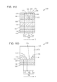
- FIG. 11C is an expanded cross-sectional side view of a beta trench along a Y direction of FIG. 11B taken along the cross-sectional line 11 C- 11 C;
- FIG. 11D is an expanded cross-sectional side view of a gamma trench along an Y direction of FIG. 11B taken along the cross-sectional line 11 D- 11 D;
- FIG. 12A is a perspective view of the structure of FIG. 11A having the mandrels anisotropically etched away to form a pattern in accordance with the present invention
- FIG. 12B is a top perspective view of FIG. 12A ;
- FIG. 13A is a perspective view of the structure of FIG. 12A having the exposed portion of the third hardmask layer anisotropically etched away in accordance with the present invention
- FIG. 13B is a top perspective view of FIG. 13A ;
- FIG. 14A is a perspective view of the structure of FIG. 13A having the exposed portion of the second hardmask layer anisotropically etched away in accordance with the present invention
- FIG. 14B is a top perspective view of FIG. 14A ;
- FIG. 15A is a perspective view of the structure of FIG. 14A having the exposed portion of the first hardmask layer anisotropically etched away in accordance with the present invention
- FIG. 15B is a top perspective view of FIG. 15A ;
- FIG. 16 is a top view of the structure of FIG. 15A having the pattern etched into a dielectric layer of the dielectric stack to form an array of alternating mandrel and non-mandrel metal lines in accordance with the present invention.
- FIGS. 1-16 illustrate various exemplary embodiments of methods of forming cuts in mandrel and/or non-mandrel metal lines through the use of a single mandrel line cut mask and/or a single non-mandrel line cut mask respectively in accordance with the present invention.
- Structure 100 includes a titanium nitride (TiN) first hardmask layer 102 disposed over a dielectric stack 104 .
- the dielectric stack 104 may include many different combinations of layers depending on such factors as application requirements, cost, design preferences and the like.
- the dielectric stack 104 includes a first silicon oxynitride dielectric layer (first SiON dielectric layer) 106 disposed over a low dielectric constant (k) layer 108 , such as a dielectric layer composed of various combinations of silicon, carbon, oxygen and hydrogen (an SiCOH layer).
- the low k dielectric layer 108 is disposed over an etch-stop layer 110 , such as a silicon nitride (SiN) layer, which is also included in the dielectric stack 104 .
- the dielectric stack 104 is disposed over a metallization layer 112 , which contains a plurality of interconnect lines 114 that make up a portion of an electrical interconnection system for structure 100 .
- Metallization layer 112 is disposed over a second SiN etch stop layer 116 .
- the second etch stop layer 116 is disposed over a complex stack of buried layers 118 from the substrate (not shown) upwards.
- a second hardmask layer 122 composed of SiN, is disposed over first hardmask layer 102 .
- a third hardmask layer 124 composed of a material such as TiN, is disposed over the second hardmask layer 122 .
- a mandrel layer 120 composed of an amorphous silicon (a-Si), is disposed over the third hardmask layer 124 .
- the combination of the three hardmask layers 102 , 122 and 124 provides the ability to etch both beta trenches 154 and gamma trenches 164 (best seen in FIG. 9 ) that will ultimately be used to form self-aligned mandrel line cuts 210 , 213 and non-mandrel line cuts 214 , 216 respectively (best seen in FIG. 16 ). It is important to note that the first hardmask layer 102 and the third hardmask layer 124 must be different enough from the second hardmask layer 122 to be etch selective relative to such second hardmask layer 122 .
- first and third hardmask layers 102 , 124 have been selected for the first and third hardmask layers 102 , 124 and SiN has been selected for the second (middle) hardmask layer 122 .
- first and third hardmask layers 102 , 124 do not have to be the same material and that many other combinations of materials for the hardmask layers 102 , 122 and 124 will work for this invention.
- the first mandrel lithographic stack 134 can be composed of several different kinds of layers, depending on such parameters as the application requirements, design or proprietary preferences or the like.
- One such stack of layers includes a stack of four thin films which includes (from top to bottom) a resist layer 136 , a bottom antireflective coating (BARC) layer 138 , a second SiON dielectric layer 140 and a spin-on hardmask (SOH) layer 142 .
- This SOH layer 142 is typically made of amorphous carbon.
- a mandrel mask (not shown) is used to pattern and print a parallel array 144 of mandrels 146 into the resist layer 136 of the mandrel lithographic stack 134 through well-known lithographic techniques.
- a pitch 147 i.e., the center to center distance between repetitive features on an integrated circuit
- the mandrels 146 are then etched and trimmed, by a variety of well-known processes, to reduce the width (indicated by arrow 148 ) of the mandrels 146 to, in this example, substantially 20 nm and to extend the mandrels down into the mandrel layer 120 .
- the width 148 of the mandrels 146 has been reduced to 20 nm, the pitch 147 of 80 nm has not changed.
- mandrels 146 will ultimately be utilized to form an array 200 of alternating mandrel metal lines 204 , 208 and non-mandrel metal lines 202 , 206 (best seen in FIG. 16 ) in the low-k dielectric layer 108 .
- the mandrel layer 120 (and therefore the mandrels 146 ), the second hardmask layer 122 and third hardmask layer 124 have different material compositions in order to be able to selectively etch features into each layer 120 , 122 , 124 in the remaining steps.
- silicon nitride (SiN) was chosen for the material of the second hardmask layer 122
- titanium nitride (TiN) was chosen for the material of the third hardmask layer
- a-Si amorphous silicon
- the mandrels 146 of the array of mandrels 144 , are next patterned into the third hardmask layer 124 to expose the second hardmask layer 122 between the mandrels. This can be done by selectively anisotropically etching the TiN of the third hardmask layer 124 but not the amorphous silicon of the mandrel layer 120 . Additionally, even though FIGS. 4 and 5 are shown as two separate steps, the same process can often do both.
- RIE Reactive Ion Etch
- Etching the mandrels 146 into the third hardmask layer 124 and exposing the second hardmask layer 122 creates two different levels for the formation of beta (mandrel) trenches 154 and gamma (non-mandrel) trenches 164 (best seen in FIG. 9 ).
- the beta and gamma trenches 154 , 164 will ultimately be used to form self-aligned mandrel line cuts 210 , 211 and non-mandrel line cuts 214 , 216 respectively in the dielectric layer 108 of the dielectric stack 104 (best seen in FIG. 16 ).
- a second beta lithographic stack 149 is disposed over the structure 100 .
- a first mandrel line cut mask (not shown) is used to pattern and print a beta opening 150 into a predetermined location of resist layer 152 of stack 149 .
- first mandrel line cut 210 and a second mandrel line cut 211 which are collectively referred to herein as a first pair of mandrel line cuts 210 , 211 (best seen in FIG. 16 ).
- the first pair of mandrel line cuts 210 , 211 will be disposed in a selected mandrel line 204 of the array 200 of metal lines 202 , 204 , 206 and 208 (herein 202 - 208 ).
- the first pair of mandrel line cuts 210 , 211 will be self-aligned in the Y direction 203 (best seen in FIG.
- the width 153 of the beta opening 150 must be substantially equal to the combined width 228 (best seen in FIG. 16 ) of the width 212 of the first mandrel line cut 210 plus the width 213 of the second mandrel line cut 211 plus the edge-to-edge distance 225 between the cuts 210 , 211 . Assuming that the mandrel line cut widths 212 and 213 are substantially equal, then it can be said that the width 153 of the beta opening 150 (as well as the combined width 228 as illustrated in FIG.
- the beta opening 150 is positioned such that it is located directly above the selected mandrel line 204 and extends laterally in the X direction 201 (best seen in FIG. 16 ) across the entire width of the selected mandrel line 204 .
- an anisotropic etch process such as a reactive ion etch (RIE) is utilized to selectively etch a beta trench 154 entirely in a mandrel 146 of the array 144 .
- RIE reactive ion etch
- the etching process which formed beta trench 154 can be selected such that it affects only the a-Si mandrels 146 and not the TiN third hardmask layer 124 or the SiN second hardmask layer 122 . Because the pitch is still 80 nm, the overlay control of the lithographic process, which was used to size and locate the beta trench 154 , is accurate enough to prevent the etching process from over extending in the X direction past the entire width (as indicated by width arrow 156 ) of the exposed second hardmask layer 122 between mandrels 146 , making this etch self-aligned.
- a third gamma lithographic stack 158 is disposed over the structure 100 .
- a second non-mandrel line cut mask (not shown) is used to pattern and print a gamma opening 160 into a predetermined location of resist layer 162 of the stack 158 .
- the gamma opening 160 will ultimately be utilized to pattern a first non-mandrel line cut 214 and a second non-mandrel line cut 216 , which are collectively referred to herein as a second pair of non-mandrel cut lines 214 , 216 (best seen in FIG. 16 ).
- the second pair of non-mandrel line cuts 214 , 216 will be disposed in a selected non-mandrel line 206 of the metal line array 200 .
- the pair of cuts 214 , 216 will be self-aligned in the Y direction 203 (best seen in FIG. 16 ) and spaced apart by a center-to-center distance 218 in the Y direction that is less than 100 nm.
- the width 161 of the gamma opening 160 must be substantially equal to the combined width 226 (best seen in FIG. 16 ) of the width 220 of the first non-mandrel line cut 214 plus the width 222 of the second non-mandrel line cut 216 plus the edge-to-edge distance 224 between the cuts 214 , 216 .
- the width 161 of the gamma opening 160 (as well as the combined width 226 as illustrated in FIG. 16 ) is substantially equal to the width of a non-mandrel line cut ( 220 or 222 ) plus the center-to-center distance 218 between the cuts 214 , 216 .
- another anisotropic etch process such as a RIE, is utilized to selectively etch a gamma trench 164 entirely into and through the second hardmask layer 122 to expose the top surface of the first hardmask layer 102 (best seen in FIG. 9B ). More precisely the gamma trench 164 is etched in the exposed area of second hardmask layer 122 between the mandrels 146 and extends down to the top surface of the first hardmask layer 102 . The gamma trench 164 is substantially equal in width 165 to the width 156 of exposed second hardmask layer. The shape of the gamma trench 164 will eventually be further altered and patterned down to the low k dielectric layer 108 to form the self-aligned second pair of non-mandrel line cuts 214 and 216 discussed earlier.
- a RIE anisotropic etch process
- the etching process which formed gamma trench 164 can be selected such that it affects only the SiN second hardmask layer 122 and not the a-Si mandrels 146 or the TiN third hardmask layer 124 . Because the pitch is still 80 nm, the overlay control of the lithographic process, which was used to size and locate the gamma trench 164 , is accurate enough to prevent the etching process from over extending in the X direction past the entire width 156 of the exposed second hardmask layer 122 between mandrels 146 plus the width 148 of the two adjacent mandrels 146 .
- the spacer layer 166 is a silicon dioxide (SiO2) thin film, which is conformally coated over the mandrels 146 , exposed third hardmask layer 124 within the beta trench 154 , exposed second hardmask layer 122 and exposed first hardmask layer 102 within the gamma trench 164 .
- the SiO2 material composition of the spacer layer 166 was chosen to be different from that of the mandrel layer 120 , third hardmask layer 124 and second hardmask layer 122 . Other materials for the spacer layer 166 may also be used.
- the material composition of the spacer layer 166 be different enough to enable selective etching between any combination of the mandrel layer 120 (and therefore the mandrels 146 ), the third hardmask layer 124 , the second hardmask layer 122 and the spacer layer 166 .
- the spacer layer 166 does not fill and plug the beta trench 154 and gamma trench 164 . Rather the spacer layer 166 conformally coats the floor of the gamma trench 164 (i.e., the top surface of the first hardmask layer 102 within the gamma trench 164 ) without completely plugging the gamma trench 164 . Additionally, the spacer layer 166 conformally coats the floor of the beta trench 154 (i.e., the top surface of the third hardmask layer 124 within the beta trench 154 ) without completely plugging the beta trench 154 .
- the spacer layer 166 can be applied by a deposition process, such as an atomic layer deposition (ALD) process, which can precisely control the spacer layer thickness 167 . In this embodiment, the spacer layer thickness is controlled to substantially 20 nm.
- ALD atomic layer deposition
- FIGS. 11A , B, C and D wherein: FIG. 11A is a perspective view of the structure 100 of FIG. 10 after being anisotropically etched and FIG. 11B is a perspective top view of FIG. 11A .
- FIG. 11C is an expanded cross-sectional side view of beta trench 154 along the Y direction of FIG. 11B taken along the cross-sectional line 11 C- 11 C.
- FIG. 11D is an expanded cross-sectional side view of gamma trench 164 along the Y direction of FIG. 11B taken along the cross-sectional line 11 D- 11 D.
- the spacer layer 166 is anisotropically etched, such as by a RIE process, to expose a portions of the top surface of the second hardmask layer 122 and to expose the upper surface of the mandrels 146 .
- the anisotropic etch also exposes a portion 168 of the top surface of the third hardmask layer 124 within the beta trench 154 (best seen in FIG. 11C ).
- the anisotropic etching process also exposes a portion 179 of the top surface of the first hardmask layer 102 within the gamma trench 164 (best seen in FIG. 11D ).
- the anisotropic etching process forms an array of first spacers 172 disposed on sidewalls of the mandrels 146 and extending longitudinally in the Y direction (best seen in FIG. 11B ). Since the anisotropic etching process etches in the vertical direction only, the remaining first spacers have a spacer width 174 (best seen in FIG. 11B ) that is substantially equal to the original spacer layer thickness 167 of 20 nm. Additionally, since the spacing between the spacers 172 is defined by the existing structure of the sidewalls of the mandrels 146 (best seen in FIG. 11B ), the spacers 172 are considered to be self-aligned in the X direction.
- the anisotropic etching process forms a pair of first inner spacers 175 disposed on the inner sidewalls 177 of beta trench 154 (best seen in FIG. 11C ). Because the spacing between the first inner spacers 175 is defined by the existing structure of the sidewalls 177 of beta trench 154 , the first inner spacers 175 are considered to be self-aligned in the Y direction.
- the exposed portion 168 of the top surface of the third hardmask 124 separates the first inner spacers 175 by a predetermined edge-to-edge distance 181 in the Y direction. Accordingly, the exposed portion 168 of the third hardmask layer 124 within beta trench 154 forms the floor of beta trench 154 .
- the first inner spacers 175 have the same spacer width 174 as the first spacers 172 , which is substantially equal to the original spacer layer thickness 167 of 20 nm.
- the anisotropic etching process also forms a pair of second inner spacers 176 disposed on inner sidewalls 178 of gamma trench 164 (best seen in FIG. 11D ). Because the spacing between the inner spacers 176 is defined by the existing structure of the sidewalls 178 of gamma trench 164 , the inner spacers 176 are considered to be self-aligned in the Y direction.
- the exposed portion 179 of the top surface of the first hardmask 102 separates the inner spacers 176 by a predetermined edge-to-edge distance 180 in the Y direction. Accordingly, the exposed portion 179 of top mask layer 102 within gamma trench 164 forms the floor of gamma trench 164 .
- the second inner spacers 176 have the same spacer width 174 as the first spacers 172 , which is substantially equal to the original spacer layer thickness 167 of 20 nm.
- the first inner spacers 175 will be used as blocks when patterning down to form the first and second mandrel line cuts 210 and 211 , wherein the spacer width 174 will determine the mandrel line cut widths 212 , 213 and the predetermined distance 181 between the first inner spacers 175 will determine the edge-to-edge distance 225 between the mandrel line cuts 210 and 211 .
- the inner spacers 176 will be used as blocks when patterning down to form the first and second non-mandrel line cuts 214 and 216 , wherein the spacer width 174 will determine the non-mandrel line cut widths 220 , 222 and the predetermined distance 180 between the inner spacers 176 will determine the edge-to-edge distance 224 between the non-mandrel line cuts 214 and 216 .
- the center-to-center distance 219 between the mandrel line cuts 210 , 211 , as well as the center-to-center distance 218 between the non-mandrel line cuts 214 , 216 can be made much smaller than 100 nm. More specifically the center-to-center distances 219 and 218 between cuts 210 , 211 and between cuts 214 , 216 can be smaller than 50 nm or even smaller than 25 nm.
- the a-Si mandrels 146 are selectively etched away, leaving the first spacers 172 , the first inner spacers 175 and the second inner spacers 176 .
- the result of the etching process is that a pattern 182 of array 200 (best seen in FIG. 16 ) has emerged over the structure 100 .
- the exposed portions of the second and third hardmask layers 122 , 124 of pattern 182 will define the alternating mandrel metal lines 204 , 208 and non-mandrel metal lines 202 , 206 of array 200 .
- the first spacers 172 of pattern 182 will define the distance between the metal lines 200 - 208 .
- the first inner spacers 175 of pattern 182 will define the self-aligned mandrel line cuts 210 and 211 .
- the edge-to-edge distance 181 of the exposed portion 168 of the third hardmask layer 124 of pattern 182 will define the edge-to-edge distance 225 between the mandrel line cuts 210 , 211 .
- the second inner spacers 176 of pattern 182 will define the self-aligned non-mandrel line cuts 214 and 216 .
- the edge-to-edge distance 180 of the exposed portion 179 of the first hardmask layer 102 of pattern 182 will define the edge-to-edge distance 225 between the non-mandrel line cuts 214 , 216 .
- the pitch of the array of first spacers 172 on structure 100 is now half the pitch of that of the array of mandrels 146 . That is, the pitch has been halved from 80 nm to 40 nm on the structure 100 .
- this example shows a mandrel pitch of 80 nm and a spacer pitch of 40 nm, one skilled in the art would recognize that this method of forming a pattern may be used with other pitches.
- the mandrel array may have a pitch of 100 nm or less
- the spacer array may have a pitch of 50 nm or less.
- the exposed portions of the TiN third hardmask layer 124 , and the exposed TiN portion 179 of the first hardmask layer 102 within the gamma trench 164 are anisotropically etched away so that the pattern 182 now is primarily over the second hardmask layer 122 .
- the exposed portions of second hardmask layer 122 are now anisotropically etched away so that the pattern 182 now is over the first hardmask layer 102 .
- the exposed portions of the first hardmask layer 102 are anisotropically etched away to form the pattern 182 directly over the first SION dielectric layer 106 of the dielectric stack 104 .
- An added benefit to this method of forming the pattern 182 is that the sequential selective etching to remove the a-Si mandrels 146 , the exposed portions of the SiN second hardmask layer 122 and the exposed portions of the TiN first and third hardmask layers 102 , 124 may be accomplished in a single integrated etch process. That is, through well-known RIE techniques, the composition of the reactive plasma of the RIE process can be changed as it penetrates through the mandrels 146 , the third hardmask layer 124 , the second hardmask layer 122 and the first hardmask layer 102 to stop at the first dielectric layer 106 at the top of the dielectric stack 104 .
- the first hardmask layer 102 is composed of TiN and is, therefore, very etch selective from that of the other materials above and below the hardmask layer 102 . Therefore all other materials above the first hardmask layer 102 can be readily stripped away using well-known techniques to expose the pattern 182 in the TiN first hardmask layer. At this point in the process we are ready to etch the pattern 182 to form trenches (not shown) in the low k dielectric layer 108 . The trenches will then be metalized to form the metal array 200 of FIG. 16 .
- the metal line array 200 is a typical SRAM cell that is now formed into low k dielectric layer 108 .
- the array includes the alternating mandrel metal lines 204 , 208 and non-mandrel metal lines 202 , 206 , which are self-aligned in the X direction.
- each metal line 202 - 208 is 20 nm thick and spaced apart a distance of 20 nm, therefore the repetitive pitch is 40 nm.
- Mandrel line 204 now includes the two mandrel line cuts 210 and 211 (collectively, the first pair of mandrel line cuts), which have cut widths 212 , 213 respectively that are substantially equal to the spacer layer width 167 and, therefore the spacer width 174 .
- the cut widths 212 , 213 are substantially 20 nm.
- the first pair of mandrel line cuts 210 and 211 are advantageously self-aligned in the Y direction since they were formed from the previously self-aligned first inner spacers 175 . Also advantageously, because the mandrel line cuts 210 , 211 were formed from the self-aligned first inner spacers 175 , their formation process was not limited by lithographic resolution.
- the center-to-center distance 219 between the mandrel line cuts 210 , 211 can be made much smaller than 100 nm. More specifically the center-to-center distance 219 between the first pair of mandrel line cuts 210 , 211 can be smaller than 50 nm or even smaller than 25 nm.
- Non-mandrel line 206 now includes the two non-mandrel line cuts 214 and 216 (collectively, the second pair of non-mandrel line cuts), which have cut widths 220 , 222 respectively that are substantially equal to the spacer layer width 167 and, therefore the spacer width 174 .
- the cut widths 220 , 222 are substantially 20 nm.
- the cuts 214 and 216 are advantageously self-aligned in the Y direction since they were formed from the previously self-aligned second inner spacers 176 . Also advantageously, because the non-mandrel line cuts 214 , 216 were formed from the self-aligned inner spacers 176 , their formation process was not limited by lithographic resolution.
- the center-to-center distance 218 between the non-mandrel line cuts 214 , 216 can be made much smaller than 100 nm. More specifically the center-to-center distance 218 between cuts 214 , 216 can be smaller than 50 nm or even smaller than 25 nm.
- non-mandrel line cuts were formed through the use of a single non-mandrel line cut mask and the mandrel line cuts were formed through the use of a single mandrel line cut mask. No additional cut masks were used to make the separate non-mandrel line cuts or the separate mandrel line cuts. As a result, costs of additional cut masks were avoided as well as the associated lithographic overlay problems associated with the use of additional cut masks.
- this method of forming self-aligned line cuts provides the flexibility of forming either self-aligned mandrel line cuts, non-mandrel line cuts or both. More specifically, a beta trench 154 may be patterned into the mandrels 146 to form a first pair of mandrel line cuts 210 , 211 and/or a gamma trench 164 may be patterned into the second hardmask layer 122 to form a second pair of non-mandrel line cuts 214 , 216 .
Abstract
Description
Claims (16)
Priority Applications (3)
| Application Number | Priority Date | Filing Date | Title |
|---|---|---|---|
| US15/271,497 US9818641B1 (en) | 2016-09-21 | 2016-09-21 | Apparatus and method of forming self-aligned cuts in mandrel and a non-mandrel lines of an array of metal lines |
| TW106115283A TWI657503B (en) | 2016-09-21 | 2017-05-09 | Apparatus and method of forming self-aligned cuts in mandrel and a non-mandrel lines of an array of metal lines |
| CN201710858640.XA CN107863308B (en) | 2016-09-21 | 2017-09-21 | Apparatus and method for forming self-aligned cuts in mandrels and non-mandrel axes of an array of metal wires |
Applications Claiming Priority (1)
| Application Number | Priority Date | Filing Date | Title |
|---|---|---|---|
| US15/271,497 US9818641B1 (en) | 2016-09-21 | 2016-09-21 | Apparatus and method of forming self-aligned cuts in mandrel and a non-mandrel lines of an array of metal lines |
Publications (1)
| Publication Number | Publication Date |
|---|---|
| US9818641B1 true US9818641B1 (en) | 2017-11-14 |
Family
ID=60255657
Family Applications (1)
| Application Number | Title | Priority Date | Filing Date |
|---|---|---|---|
| US15/271,497 Expired - Fee Related US9818641B1 (en) | 2016-09-21 | 2016-09-21 | Apparatus and method of forming self-aligned cuts in mandrel and a non-mandrel lines of an array of metal lines |
Country Status (3)
| Country | Link |
|---|---|
| US (1) | US9818641B1 (en) |
| CN (1) | CN107863308B (en) |
| TW (1) | TWI657503B (en) |
Cited By (20)
| Publication number | Priority date | Publication date | Assignee | Title |
|---|---|---|---|---|
| US20180247862A1 (en) * | 2017-02-27 | 2018-08-30 | Imec Vzw | Method for Defining Patterns for Conductive Paths in Dielectric Layer |
| US20180308753A1 (en) * | 2017-04-19 | 2018-10-25 | Tokyo Electron Limited | Process Integration Techniques Using A Carbon Layer To Form Self-Aligned Structures |
| US10199270B2 (en) * | 2017-05-25 | 2019-02-05 | Globalfoundries Inc. | Multi-directional self-aligned multiple patterning |
| US10347583B1 (en) | 2018-01-02 | 2019-07-09 | Globalfoundries Inc. | Methods of patterning dielectric layers for metallization and related structures |
| US10366917B2 (en) * | 2018-01-04 | 2019-07-30 | Globalfoundries Inc. | Methods of patterning variable width metallization lines |
| CN110391209A (en) * | 2018-04-23 | 2019-10-29 | 格芯公司 | Electric fuse during multiple Patternized technique is formed |
| US10651046B2 (en) | 2018-10-08 | 2020-05-12 | Globalfoundries Inc. | Multiple patterning with late lithographically-defined mandrel cuts |
| US10784119B2 (en) | 2018-10-08 | 2020-09-22 | Globalfoundries Inc. | Multiple patterning with lithographically-defined cuts |
| EP3840034A1 (en) * | 2019-12-19 | 2021-06-23 | Imec VZW | A semiconductor fabrication method for producing nanoscaled electrically conductive lines |
| US11127627B2 (en) | 2018-11-27 | 2021-09-21 | Imec Vzw | Method for forming an interconnection structure |
| US11152261B2 (en) | 2019-10-26 | 2021-10-19 | International Business Machines Corporation | Self-aligned top via formation at line ends |
| US11158536B2 (en) | 2020-01-07 | 2021-10-26 | International Business Machines Corporation | Patterning line cuts before line patterning using sacrificial fill material |
| EP3901986A1 (en) * | 2020-04-23 | 2021-10-27 | IMEC vzw | A patterning method |
| EP3901987A1 (en) * | 2020-04-23 | 2021-10-27 | IMEC vzw | A patterning method |
| US11195795B1 (en) | 2020-06-03 | 2021-12-07 | International Business Machines Corporation | Well-controlled edge-to-edge spacing between adjacent interconnects |
| US11276639B2 (en) | 2020-01-22 | 2022-03-15 | International Business Machines Corporation | Conductive lines with subtractive cuts |
| US11373880B2 (en) | 2020-09-22 | 2022-06-28 | International Business Machines Corporation | Creating different width lines and spaces in a metal layer |
| US11417525B2 (en) | 2018-10-08 | 2022-08-16 | Globalfoundries U.S. Inc. | Multiple patterning with mandrel cuts defined by block masks |
| US11527434B2 (en) | 2020-02-20 | 2022-12-13 | International Business Machines Corporation | Line cut patterning using sacrificial material |
| US20240096627A1 (en) * | 2017-01-11 | 2024-03-21 | Tessera Llc | Self aligned pattern formation post spacer etchback in tight pitch configurations |
Citations (44)
| Publication number | Priority date | Publication date | Assignee | Title |
|---|---|---|---|---|
| US6455436B1 (en) | 1999-01-08 | 2002-09-24 | Matsushita Electric Industrial Co., Ltd. | Method of fabricating semiconductor device |
| US20050215040A1 (en) | 2000-03-01 | 2005-09-29 | Brian Doyle | Quantum wire gate device and method of making same |
| US20060055045A1 (en) | 2004-09-10 | 2006-03-16 | Chul-Woo Park | Semiconductor memory device and arrangement method thereof |
| US7183142B2 (en) | 2005-01-13 | 2007-02-27 | International Business Machines Corporation | FinFETs with long gate length at high density |
| US20080193658A1 (en) | 2007-02-08 | 2008-08-14 | Micron Technology, Inc. | Methods using block copolymer self-assembly for sub-lithographic patterning |
| US20080227298A1 (en) | 2007-03-15 | 2008-09-18 | Elpida Memory, Inc. | Semiconductor device manufacturing method |
| US20110256723A1 (en) | 2010-04-15 | 2011-10-20 | Hynix Semiconductor Inc. | Method for forming semiconductor device |
| US20110316125A1 (en) | 2004-08-19 | 2011-12-29 | Micron Technology, Inc. | Intermediate structures for forming circuits |
| US20120118854A1 (en) | 2010-11-12 | 2012-05-17 | Tela Innovations, Inc. | Methods for linewidth modification and apparatus implementing the same |
| US20120132988A1 (en) | 2010-03-24 | 2012-05-31 | Alpha And Omega Semiconductor Incorporated | Oxide terminated trench mosfet with three or four masks |
| US8298943B1 (en) | 2011-05-27 | 2012-10-30 | International Business Machines Corporation | Self aligning via patterning |
| US20130196517A1 (en) | 2012-01-31 | 2013-08-01 | Canon Kabushiki Kaisha | Drawing method and method of manufacturing article |
| US20130244344A1 (en) | 2008-02-29 | 2013-09-19 | Roger Klas Malmhall | Method for manufacturing high density non-volatile magnetic memory |
| US20130329486A1 (en) | 2008-04-03 | 2013-12-12 | Micron Technology, Inc. | Data Cells with Drivers and Methods of Making and Operating the Same |
| US20140038428A1 (en) | 2012-08-06 | 2014-02-06 | Taiwan Semiconductor Manufacturing Co. Ltd. | Self-Assembled Monolayer for Pattern Formation |
| US20140054534A1 (en) | 2012-08-23 | 2014-02-27 | Micron Technology, Inc. | Self-aligned interconnection for integrated circuits |
| US20140170853A1 (en) | 2012-12-14 | 2014-06-19 | Lam Research Corporation | Image reversal with ahm gap fill for multiple patterning |
| US20140258961A1 (en) | 2013-03-11 | 2014-09-11 | Taiwan Semiconductor Manufacturing Company, Ltd. | Stretch Dummy Cell Insertion in FinFET Process |
| US20140273363A1 (en) * | 2013-03-14 | 2014-09-18 | Taiwan Semiconductor Manufacturing Company, Ltd. | Method of patterning features of a semiconductor device |
| US20140273464A1 (en) * | 2013-03-12 | 2014-09-18 | Taiwan Semiconductor Manufacturing Company, Ltd. | Method of Fabricating a FinFET Device |
| US20150056800A1 (en) | 2013-08-20 | 2015-02-26 | Bencherki Mebarki | Self-aligned interconnects formed using substractive techniques |
| US20150072527A1 (en) | 2012-02-09 | 2015-03-12 | Taiwan Semiconductor Manufacturing Company, Ltd. | Method for patterning a plurality of features for fin-like field-effect transistor (finfet) devices |
| US20150087149A1 (en) | 2013-09-26 | 2015-03-26 | GlobalFoundries, Inc. | Methods for fabricating integrated circuits using improved masks |
| US8999848B2 (en) | 2012-07-12 | 2015-04-07 | SK Hynix Inc. | Method for forming fine pattern of semiconductor device using double spacer patterning technology |
| US9012287B2 (en) | 2012-11-14 | 2015-04-21 | Taiwan Semiconductor Manufacturing Company, Ltd. | Cell layout for SRAM FinFET transistors |
| US20150108087A1 (en) | 2013-10-20 | 2015-04-23 | Tokyo Electron Limited | Use of grapho-epitaxial directed self-assembly to precisely cut lines |
| US20150140811A1 (en) | 2013-11-20 | 2015-05-21 | Taiwan Semiconductor Manufacturing Company, Ltd. | Spacer-Damage-Free Etching |
| US20150147882A1 (en) | 2013-11-22 | 2015-05-28 | Taiwan Semiconductor Manufacturing Company, Ltd. | Integrated Circuits with Reduced Pitch and Line Spacing and Methods of Forming the Same |
| US20150179652A1 (en) * | 2012-03-11 | 2015-06-25 | United Microelectronics Corp. | Patterned structure of semiconductor device |
| US20150243654A1 (en) | 2012-08-28 | 2015-08-27 | Institute of Microelectronics, Chinese Academy of Sciences | Semiconductor structure and method for manufacturing the same |
| US9123656B1 (en) | 2014-05-13 | 2015-09-01 | Taiwan Semiconductor Manufacturing Co., Ltd. | Organosilicate polymer mandrel for self-aligned double patterning process |
| US9136106B2 (en) | 2013-12-19 | 2015-09-15 | Taiwan Semiconductor Manufacturing Company, Ltd. | Method for integrated circuit patterning |
| US20150318173A1 (en) | 2014-05-02 | 2015-11-05 | Taiwan Semiconductor Manufacturing Company, Ltd. | Method of Semiconductor Integrated Circuit Fabrication |
| US20150339422A1 (en) | 2014-05-23 | 2015-11-26 | International Business Machines Corporation | Stitch-derived via structures and methods of generating the same |
| US9209279B1 (en) | 2014-09-12 | 2015-12-08 | Applied Materials, Inc. | Self aligned replacement fin formation |
| US20160049307A1 (en) | 2014-08-15 | 2016-02-18 | Yijian Chen | Patterning method for IC fabrication using 2-D layout decomposition and synthesis techniques |
| US20160056104A1 (en) | 2014-08-20 | 2016-02-25 | Globalfoundries Inc. | Self-aligned back end of line cut |
| US20160056075A1 (en) | 2014-08-20 | 2016-02-25 | Globalfoundries Inc. | Precut metal lines |
| US20160064248A1 (en) | 2013-03-14 | 2016-03-03 | Taiwan Semiconductor Manufacturing Co., Ltd. | Double patterning method |
| US20160086841A1 (en) | 2014-09-19 | 2016-03-24 | Samsung Electronics Co., Ltd. | Method for forming pattern of semiconductor device and semiconductor device formed using the same |
| US20160099178A1 (en) | 2014-10-05 | 2016-04-07 | Applied Materials, Inc. | Fin structure formation by selective etching |
| US9406775B1 (en) | 2015-04-27 | 2016-08-02 | Globalfoundries Inc. | Method for creating self-aligned compact contacts in an IC device meeting fabrication spacing constraints |
| US20160225634A1 (en) | 2015-02-04 | 2016-08-04 | International Business Machines Corporation | Method for quadruple frequency finfets with single-fin removal |
| US20160254191A1 (en) | 2015-02-26 | 2016-09-01 | Taiwan Semiconductor Manufacturing Company, Ltd. | Fin patterning methods for increased process margin |
Family Cites Families (7)
| Publication number | Priority date | Publication date | Assignee | Title |
|---|---|---|---|---|
| JP2009231372A (en) * | 2008-03-19 | 2009-10-08 | Toshiba Corp | Pattern formation method |
| US8513129B2 (en) * | 2010-05-28 | 2013-08-20 | Applied Materials, Inc. | Planarizing etch hardmask to increase pattern density and aspect ratio |
| US9111857B2 (en) * | 2012-09-21 | 2015-08-18 | Micron Technology, Inc. | Method, system and device for recessed contact in memory array |
| CN102881648B (en) * | 2012-10-17 | 2016-09-14 | 上海华虹宏力半导体制造有限公司 | The manufacture method of metal interconnection structure |
| KR102377372B1 (en) * | 2014-04-02 | 2022-03-21 | 어플라이드 머티어리얼스, 인코포레이티드 | Method for forming interconnects |
| CN106575650B (en) * | 2014-05-08 | 2019-10-18 | 英特尔公司 | Constriction for integrated circuit interconnects fuse-wires structure |
| KR102323456B1 (en) * | 2014-12-26 | 2021-11-10 | 삼성전자주식회사 | A semiconductor device and method for fabricating the semiconductor device |
-
2016
- 2016-09-21 US US15/271,497 patent/US9818641B1/en not_active Expired - Fee Related
-
2017
- 2017-05-09 TW TW106115283A patent/TWI657503B/en active
- 2017-09-21 CN CN201710858640.XA patent/CN107863308B/en active Active
Patent Citations (47)
| Publication number | Priority date | Publication date | Assignee | Title |
|---|---|---|---|---|
| US6455436B1 (en) | 1999-01-08 | 2002-09-24 | Matsushita Electric Industrial Co., Ltd. | Method of fabricating semiconductor device |
| US20050215040A1 (en) | 2000-03-01 | 2005-09-29 | Brian Doyle | Quantum wire gate device and method of making same |
| US20110316125A1 (en) | 2004-08-19 | 2011-12-29 | Micron Technology, Inc. | Intermediate structures for forming circuits |
| US20060055045A1 (en) | 2004-09-10 | 2006-03-16 | Chul-Woo Park | Semiconductor memory device and arrangement method thereof |
| US7183142B2 (en) | 2005-01-13 | 2007-02-27 | International Business Machines Corporation | FinFETs with long gate length at high density |
| US20080193658A1 (en) | 2007-02-08 | 2008-08-14 | Micron Technology, Inc. | Methods using block copolymer self-assembly for sub-lithographic patterning |
| US20110240596A1 (en) | 2007-02-08 | 2011-10-06 | Micron Technology, Inc. | Methods Using Block Co-Polymer Self-Assembly for Sub-Lithographic Patterning |
| US20080227298A1 (en) | 2007-03-15 | 2008-09-18 | Elpida Memory, Inc. | Semiconductor device manufacturing method |
| US20130244344A1 (en) | 2008-02-29 | 2013-09-19 | Roger Klas Malmhall | Method for manufacturing high density non-volatile magnetic memory |
| US20130329486A1 (en) | 2008-04-03 | 2013-12-12 | Micron Technology, Inc. | Data Cells with Drivers and Methods of Making and Operating the Same |
| US20120132988A1 (en) | 2010-03-24 | 2012-05-31 | Alpha And Omega Semiconductor Incorporated | Oxide terminated trench mosfet with three or four masks |
| US20110256723A1 (en) | 2010-04-15 | 2011-10-20 | Hynix Semiconductor Inc. | Method for forming semiconductor device |
| US20120118854A1 (en) | 2010-11-12 | 2012-05-17 | Tela Innovations, Inc. | Methods for linewidth modification and apparatus implementing the same |
| US8518824B2 (en) * | 2011-05-27 | 2013-08-27 | International Business Machines Corporation | Self aligning via patterning |
| US8298943B1 (en) | 2011-05-27 | 2012-10-30 | International Business Machines Corporation | Self aligning via patterning |
| US20130196517A1 (en) | 2012-01-31 | 2013-08-01 | Canon Kabushiki Kaisha | Drawing method and method of manufacturing article |
| US20150072527A1 (en) | 2012-02-09 | 2015-03-12 | Taiwan Semiconductor Manufacturing Company, Ltd. | Method for patterning a plurality of features for fin-like field-effect transistor (finfet) devices |
| US20150179652A1 (en) * | 2012-03-11 | 2015-06-25 | United Microelectronics Corp. | Patterned structure of semiconductor device |
| US8999848B2 (en) | 2012-07-12 | 2015-04-07 | SK Hynix Inc. | Method for forming fine pattern of semiconductor device using double spacer patterning technology |
| US20140038428A1 (en) | 2012-08-06 | 2014-02-06 | Taiwan Semiconductor Manufacturing Co. Ltd. | Self-Assembled Monolayer for Pattern Formation |
| US20140054534A1 (en) | 2012-08-23 | 2014-02-27 | Micron Technology, Inc. | Self-aligned interconnection for integrated circuits |
| US20150243654A1 (en) | 2012-08-28 | 2015-08-27 | Institute of Microelectronics, Chinese Academy of Sciences | Semiconductor structure and method for manufacturing the same |
| US9012287B2 (en) | 2012-11-14 | 2015-04-21 | Taiwan Semiconductor Manufacturing Company, Ltd. | Cell layout for SRAM FinFET transistors |
| US20140170853A1 (en) | 2012-12-14 | 2014-06-19 | Lam Research Corporation | Image reversal with ahm gap fill for multiple patterning |
| US20140258961A1 (en) | 2013-03-11 | 2014-09-11 | Taiwan Semiconductor Manufacturing Company, Ltd. | Stretch Dummy Cell Insertion in FinFET Process |
| US20140273464A1 (en) * | 2013-03-12 | 2014-09-18 | Taiwan Semiconductor Manufacturing Company, Ltd. | Method of Fabricating a FinFET Device |
| US20140273363A1 (en) * | 2013-03-14 | 2014-09-18 | Taiwan Semiconductor Manufacturing Company, Ltd. | Method of patterning features of a semiconductor device |
| US20160064248A1 (en) | 2013-03-14 | 2016-03-03 | Taiwan Semiconductor Manufacturing Co., Ltd. | Double patterning method |
| US20150056800A1 (en) | 2013-08-20 | 2015-02-26 | Bencherki Mebarki | Self-aligned interconnects formed using substractive techniques |
| US20150087149A1 (en) | 2013-09-26 | 2015-03-26 | GlobalFoundries, Inc. | Methods for fabricating integrated circuits using improved masks |
| US20150108087A1 (en) | 2013-10-20 | 2015-04-23 | Tokyo Electron Limited | Use of grapho-epitaxial directed self-assembly to precisely cut lines |
| US20150140811A1 (en) | 2013-11-20 | 2015-05-21 | Taiwan Semiconductor Manufacturing Company, Ltd. | Spacer-Damage-Free Etching |
| US20170221702A1 (en) | 2013-11-22 | 2017-08-03 | Taiwan Semiconductor Manufacturing Company, Ltd. | Method of Double Patterning Lithography Process Using Plurality of Mandrels for Integrated Circuit Applications |
| US20150147882A1 (en) | 2013-11-22 | 2015-05-28 | Taiwan Semiconductor Manufacturing Company, Ltd. | Integrated Circuits with Reduced Pitch and Line Spacing and Methods of Forming the Same |
| US9136106B2 (en) | 2013-12-19 | 2015-09-15 | Taiwan Semiconductor Manufacturing Company, Ltd. | Method for integrated circuit patterning |
| US20150318173A1 (en) | 2014-05-02 | 2015-11-05 | Taiwan Semiconductor Manufacturing Company, Ltd. | Method of Semiconductor Integrated Circuit Fabrication |
| US9123656B1 (en) | 2014-05-13 | 2015-09-01 | Taiwan Semiconductor Manufacturing Co., Ltd. | Organosilicate polymer mandrel for self-aligned double patterning process |
| US20150339422A1 (en) | 2014-05-23 | 2015-11-26 | International Business Machines Corporation | Stitch-derived via structures and methods of generating the same |
| US20160049307A1 (en) | 2014-08-15 | 2016-02-18 | Yijian Chen | Patterning method for IC fabrication using 2-D layout decomposition and synthesis techniques |
| US20160056075A1 (en) | 2014-08-20 | 2016-02-25 | Globalfoundries Inc. | Precut metal lines |
| US20160056104A1 (en) | 2014-08-20 | 2016-02-25 | Globalfoundries Inc. | Self-aligned back end of line cut |
| US9209279B1 (en) | 2014-09-12 | 2015-12-08 | Applied Materials, Inc. | Self aligned replacement fin formation |
| US20160086841A1 (en) | 2014-09-19 | 2016-03-24 | Samsung Electronics Co., Ltd. | Method for forming pattern of semiconductor device and semiconductor device formed using the same |
| US20160099178A1 (en) | 2014-10-05 | 2016-04-07 | Applied Materials, Inc. | Fin structure formation by selective etching |
| US20160225634A1 (en) | 2015-02-04 | 2016-08-04 | International Business Machines Corporation | Method for quadruple frequency finfets with single-fin removal |
| US20160254191A1 (en) | 2015-02-26 | 2016-09-01 | Taiwan Semiconductor Manufacturing Company, Ltd. | Fin patterning methods for increased process margin |
| US9406775B1 (en) | 2015-04-27 | 2016-08-02 | Globalfoundries Inc. | Method for creating self-aligned compact contacts in an IC device meeting fabrication spacing constraints |
Non-Patent Citations (12)
| Title |
|---|
| U.S. Appl. No. 15/053,818, filed Feb. 25, 2016. |
| U.S. Appl. No. 15/077,384, filed Mar. 22, 2016. |
| U.S. Appl. No. 15/077,480, filed Mar. 22, 2016. |
| U.S. Appl. No. 15/077,564, filed Mar. 22, 2016. |
| U.S. Appl. No. 15/141,087, filed Apr. 28, 2016. |
| U.S. Appl. No. 15/271,475, filed Sep. 21, 2016. |
| U.S. Appl. No. 15/271,519, filed Sep. 21, 2016. |
| U.S. Appl. No. 15/362,035, filed Nov. 28, 2016. |
| U.S. Appl. No. 15/379,605, filed Dec. 15, 2016. |
| U.S. Appl. No. 15/379,645, filed Dec. 15, 2016. |
| U.S. Appl. No. 15/379,707, filed Dec. 15, 2016. |
| U.S. Appl. No. 15/379,740, filed Dec. 15, 2016. |
Cited By (28)
| Publication number | Priority date | Publication date | Assignee | Title |
|---|---|---|---|---|
| US20240096627A1 (en) * | 2017-01-11 | 2024-03-21 | Tessera Llc | Self aligned pattern formation post spacer etchback in tight pitch configurations |
| US20180247862A1 (en) * | 2017-02-27 | 2018-08-30 | Imec Vzw | Method for Defining Patterns for Conductive Paths in Dielectric Layer |
| US10651076B2 (en) * | 2017-02-27 | 2020-05-12 | Imec Vzw | Method for defining patterns for conductive paths in dielectric layer |
| US20180308753A1 (en) * | 2017-04-19 | 2018-10-25 | Tokyo Electron Limited | Process Integration Techniques Using A Carbon Layer To Form Self-Aligned Structures |
| US10600687B2 (en) * | 2017-04-19 | 2020-03-24 | Tokyo Electron Limited | Process integration techniques using a carbon layer to form self-aligned structures |
| US10199270B2 (en) * | 2017-05-25 | 2019-02-05 | Globalfoundries Inc. | Multi-directional self-aligned multiple patterning |
| US10347583B1 (en) | 2018-01-02 | 2019-07-09 | Globalfoundries Inc. | Methods of patterning dielectric layers for metallization and related structures |
| US10366917B2 (en) * | 2018-01-04 | 2019-07-30 | Globalfoundries Inc. | Methods of patterning variable width metallization lines |
| TWI684244B (en) * | 2018-01-04 | 2020-02-01 | 美商格芯(美國)集成電路科技有限公司 | Methods of patterning variable width metallization lines |
| CN110391209A (en) * | 2018-04-23 | 2019-10-29 | 格芯公司 | Electric fuse during multiple Patternized technique is formed |
| CN110391209B (en) * | 2018-04-23 | 2023-08-29 | 格芯(美国)集成电路科技有限公司 | Electric fuse formation during multiple patterning process |
| US11417525B2 (en) | 2018-10-08 | 2022-08-16 | Globalfoundries U.S. Inc. | Multiple patterning with mandrel cuts defined by block masks |
| US10651046B2 (en) | 2018-10-08 | 2020-05-12 | Globalfoundries Inc. | Multiple patterning with late lithographically-defined mandrel cuts |
| US10784119B2 (en) | 2018-10-08 | 2020-09-22 | Globalfoundries Inc. | Multiple patterning with lithographically-defined cuts |
| US11127627B2 (en) | 2018-11-27 | 2021-09-21 | Imec Vzw | Method for forming an interconnection structure |
| US11152261B2 (en) | 2019-10-26 | 2021-10-19 | International Business Machines Corporation | Self-aligned top via formation at line ends |
| US11264271B2 (en) | 2019-12-19 | 2022-03-01 | Imec Vzw | Semiconductor fabrication method for producing nano-scaled electrically conductive lines |
| EP3840034A1 (en) * | 2019-12-19 | 2021-06-23 | Imec VZW | A semiconductor fabrication method for producing nanoscaled electrically conductive lines |
| US11158536B2 (en) | 2020-01-07 | 2021-10-26 | International Business Machines Corporation | Patterning line cuts before line patterning using sacrificial fill material |
| US11791258B2 (en) | 2020-01-22 | 2023-10-17 | International Business Machines Corporation | Conductive lines with subtractive cuts |
| US11276639B2 (en) | 2020-01-22 | 2022-03-15 | International Business Machines Corporation | Conductive lines with subtractive cuts |
| US11527434B2 (en) | 2020-02-20 | 2022-12-13 | International Business Machines Corporation | Line cut patterning using sacrificial material |
| US11710637B2 (en) | 2020-04-23 | 2023-07-25 | Imec Vzw | Patterning method |
| US11476155B2 (en) | 2020-04-23 | 2022-10-18 | Imec Vzw | Patterning method |
| EP3901987A1 (en) * | 2020-04-23 | 2021-10-27 | IMEC vzw | A patterning method |
| EP3901986A1 (en) * | 2020-04-23 | 2021-10-27 | IMEC vzw | A patterning method |
| US11195795B1 (en) | 2020-06-03 | 2021-12-07 | International Business Machines Corporation | Well-controlled edge-to-edge spacing between adjacent interconnects |
| US11373880B2 (en) | 2020-09-22 | 2022-06-28 | International Business Machines Corporation | Creating different width lines and spaces in a metal layer |
Also Published As
| Publication number | Publication date |
|---|---|
| CN107863308A (en) | 2018-03-30 |
| TWI657503B (en) | 2019-04-21 |
| CN107863308B (en) | 2021-09-10 |
| TW201830521A (en) | 2018-08-16 |
Similar Documents
| Publication | Publication Date | Title |
|---|---|---|
| US9818641B1 (en) | Apparatus and method of forming self-aligned cuts in mandrel and a non-mandrel lines of an array of metal lines | |
| US9818640B1 (en) | Apparatus and method of forming self-aligned cuts in a non-mandrel line of an array of metal lines | |
| US9818611B2 (en) | Methods of forming etch masks for sub-resolution substrate patterning | |
| US8012674B2 (en) | Efficient pitch multiplication process | |
| KR101003897B1 (en) | Method of forming pitch multipled contacts | |
| US8697580B2 (en) | Method of forming patterns for semiconductor device | |
| US8003542B2 (en) | Multiple spacer steps for pitch multiplication | |
| US9679809B1 (en) | Method of forming self aligned continuity blocks for mandrel and non-mandrel interconnect lines | |
| US9786545B1 (en) | Method of forming ANA regions in an integrated circuit | |
| US9818623B2 (en) | Method of forming a pattern for interconnection lines and associated continuity blocks in an integrated circuit | |
| US9691626B1 (en) | Method of forming a pattern for interconnection lines in an integrated circuit wherein the pattern includes gamma and beta block mask portions | |
| US11854806B2 (en) | Method for pattern reduction using a staircase spacer |
Legal Events
| Date | Code | Title | Description |
|---|---|---|---|
| AS | Assignment |
Owner name: GLOBALFOUNDRIES INC., CAYMAN ISLANDS Free format text: ASSIGNMENT OF ASSIGNORS INTEREST;ASSIGNORS:BOUCHE, GUILLAUME;STEPHENS, JASON EUGENE;SIGNING DATES FROM 20160609 TO 20160610;REEL/FRAME:039818/0685 |
|
| STCF | Information on status: patent grant |
Free format text: PATENTED CASE |
|
| AS | Assignment |
Owner name: WILMINGTON TRUST, NATIONAL ASSOCIATION, DELAWARE Free format text: SECURITY AGREEMENT;ASSIGNOR:GLOBALFOUNDRIES INC.;REEL/FRAME:049490/0001 Effective date: 20181127 |
|
| AS | Assignment |
Owner name: GLOBALFOUNDRIES U.S. INC., CALIFORNIA Free format text: ASSIGNMENT OF ASSIGNORS INTEREST;ASSIGNOR:GLOBALFOUNDRIES INC.;REEL/FRAME:054633/0001 Effective date: 20201022 |
|
| AS | Assignment |
Owner name: GLOBALFOUNDRIES INC., CAYMAN ISLANDS Free format text: RELEASE BY SECURED PARTY;ASSIGNOR:WILMINGTON TRUST, NATIONAL ASSOCIATION;REEL/FRAME:054636/0001 Effective date: 20201117 |
|
| AS | Assignment |
Owner name: GLOBALFOUNDRIES U.S. INC., NEW YORK Free format text: RELEASE BY SECURED PARTY;ASSIGNOR:WILMINGTON TRUST, NATIONAL ASSOCIATION;REEL/FRAME:056987/0001 Effective date: 20201117 |
|
| FEPP | Fee payment procedure |
Free format text: MAINTENANCE FEE REMINDER MAILED (ORIGINAL EVENT CODE: REM.); ENTITY STATUS OF PATENT OWNER: LARGE ENTITY |
|
| LAPS | Lapse for failure to pay maintenance fees |
Free format text: PATENT EXPIRED FOR FAILURE TO PAY MAINTENANCE FEES (ORIGINAL EVENT CODE: EXP.); ENTITY STATUS OF PATENT OWNER: LARGE ENTITY |
|
| STCH | Information on status: patent discontinuation |
Free format text: PATENT EXPIRED DUE TO NONPAYMENT OF MAINTENANCE FEES UNDER 37 CFR 1.362 |
|
| FP | Lapsed due to failure to pay maintenance fee |
Effective date: 20211114 |