US9818604B2 - Method for depositing insulating film on recessed portion having high aspect ratio - Google Patents
Method for depositing insulating film on recessed portion having high aspect ratio Download PDFInfo
- Publication number
- US9818604B2 US9818604B2 US15/323,295 US201515323295A US9818604B2 US 9818604 B2 US9818604 B2 US 9818604B2 US 201515323295 A US201515323295 A US 201515323295A US 9818604 B2 US9818604 B2 US 9818604B2
- Authority
- US
- United States
- Prior art keywords
- insulation layer
- silicon
- reaction
- trench
- substrate
- Prior art date
- Legal status (The legal status is an assumption and is not a legal conclusion. Google has not performed a legal analysis and makes no representation as to the accuracy of the status listed.)
- Active
Links
Images


Classifications
-
- H—ELECTRICITY
- H01—ELECTRIC ELEMENTS
- H01L—SEMICONDUCTOR DEVICES NOT COVERED BY CLASS H10
- H01L21/00—Processes or apparatus adapted for the manufacture or treatment of semiconductor or solid state devices or of parts thereof
- H01L21/02—Manufacture or treatment of semiconductor devices or of parts thereof
- H01L21/02104—Forming layers
- H01L21/02107—Forming insulating materials on a substrate
- H01L21/02296—Forming insulating materials on a substrate characterised by the treatment performed before or after the formation of the layer
- H01L21/02318—Forming insulating materials on a substrate characterised by the treatment performed before or after the formation of the layer post-treatment
- H01L21/02337—Forming insulating materials on a substrate characterised by the treatment performed before or after the formation of the layer post-treatment treatment by exposure to a gas or vapour
- H01L21/0234—Forming insulating materials on a substrate characterised by the treatment performed before or after the formation of the layer post-treatment treatment by exposure to a gas or vapour treatment by exposure to a plasma
-
- H—ELECTRICITY
- H01—ELECTRIC ELEMENTS
- H01L—SEMICONDUCTOR DEVICES NOT COVERED BY CLASS H10
- H01L21/00—Processes or apparatus adapted for the manufacture or treatment of semiconductor or solid state devices or of parts thereof
- H01L21/02—Manufacture or treatment of semiconductor devices or of parts thereof
- H01L21/02104—Forming layers
- H01L21/02107—Forming insulating materials on a substrate
- H01L21/02109—Forming insulating materials on a substrate characterised by the type of layer, e.g. type of material, porous/non-porous, pre-cursors, mixtures or laminates
- H01L21/02112—Forming insulating materials on a substrate characterised by the type of layer, e.g. type of material, porous/non-porous, pre-cursors, mixtures or laminates characterised by the material of the layer
- H01L21/02123—Forming insulating materials on a substrate characterised by the type of layer, e.g. type of material, porous/non-porous, pre-cursors, mixtures or laminates characterised by the material of the layer the material containing silicon
- H01L21/02164—Forming insulating materials on a substrate characterised by the type of layer, e.g. type of material, porous/non-porous, pre-cursors, mixtures or laminates characterised by the material of the layer the material containing silicon the material being a silicon oxide, e.g. SiO2
-
- H—ELECTRICITY
- H01—ELECTRIC ELEMENTS
- H01L—SEMICONDUCTOR DEVICES NOT COVERED BY CLASS H10
- H01L21/00—Processes or apparatus adapted for the manufacture or treatment of semiconductor or solid state devices or of parts thereof
- H01L21/02—Manufacture or treatment of semiconductor devices or of parts thereof
- H01L21/02104—Forming layers
- H01L21/02107—Forming insulating materials on a substrate
- H01L21/02109—Forming insulating materials on a substrate characterised by the type of layer, e.g. type of material, porous/non-porous, pre-cursors, mixtures or laminates
- H01L21/02112—Forming insulating materials on a substrate characterised by the type of layer, e.g. type of material, porous/non-porous, pre-cursors, mixtures or laminates characterised by the material of the layer
- H01L21/02123—Forming insulating materials on a substrate characterised by the type of layer, e.g. type of material, porous/non-porous, pre-cursors, mixtures or laminates characterised by the material of the layer the material containing silicon
- H01L21/0217—Forming insulating materials on a substrate characterised by the type of layer, e.g. type of material, porous/non-porous, pre-cursors, mixtures or laminates characterised by the material of the layer the material containing silicon the material being a silicon nitride not containing oxygen, e.g. SixNy or SixByNz
-
- H—ELECTRICITY
- H01—ELECTRIC ELEMENTS
- H01L—SEMICONDUCTOR DEVICES NOT COVERED BY CLASS H10
- H01L21/00—Processes or apparatus adapted for the manufacture or treatment of semiconductor or solid state devices or of parts thereof
- H01L21/02—Manufacture or treatment of semiconductor devices or of parts thereof
- H01L21/02104—Forming layers
- H01L21/02107—Forming insulating materials on a substrate
- H01L21/02109—Forming insulating materials on a substrate characterised by the type of layer, e.g. type of material, porous/non-porous, pre-cursors, mixtures or laminates
- H01L21/02205—Forming insulating materials on a substrate characterised by the type of layer, e.g. type of material, porous/non-porous, pre-cursors, mixtures or laminates the layer being characterised by the precursor material for deposition
- H01L21/02208—Forming insulating materials on a substrate characterised by the type of layer, e.g. type of material, porous/non-porous, pre-cursors, mixtures or laminates the layer being characterised by the precursor material for deposition the precursor containing a compound comprising Si
- H01L21/02211—Forming insulating materials on a substrate characterised by the type of layer, e.g. type of material, porous/non-porous, pre-cursors, mixtures or laminates the layer being characterised by the precursor material for deposition the precursor containing a compound comprising Si the compound being a silane, e.g. disilane, methylsilane or chlorosilane
-
- H—ELECTRICITY
- H01—ELECTRIC ELEMENTS
- H01L—SEMICONDUCTOR DEVICES NOT COVERED BY CLASS H10
- H01L21/00—Processes or apparatus adapted for the manufacture or treatment of semiconductor or solid state devices or of parts thereof
- H01L21/02—Manufacture or treatment of semiconductor devices or of parts thereof
- H01L21/02104—Forming layers
- H01L21/02107—Forming insulating materials on a substrate
- H01L21/02109—Forming insulating materials on a substrate characterised by the type of layer, e.g. type of material, porous/non-porous, pre-cursors, mixtures or laminates
- H01L21/02205—Forming insulating materials on a substrate characterised by the type of layer, e.g. type of material, porous/non-porous, pre-cursors, mixtures or laminates the layer being characterised by the precursor material for deposition
- H01L21/02208—Forming insulating materials on a substrate characterised by the type of layer, e.g. type of material, porous/non-porous, pre-cursors, mixtures or laminates the layer being characterised by the precursor material for deposition the precursor containing a compound comprising Si
- H01L21/02219—Forming insulating materials on a substrate characterised by the type of layer, e.g. type of material, porous/non-porous, pre-cursors, mixtures or laminates the layer being characterised by the precursor material for deposition the precursor containing a compound comprising Si the compound comprising silicon and nitrogen
-
- H—ELECTRICITY
- H01—ELECTRIC ELEMENTS
- H01L—SEMICONDUCTOR DEVICES NOT COVERED BY CLASS H10
- H01L21/00—Processes or apparatus adapted for the manufacture or treatment of semiconductor or solid state devices or of parts thereof
- H01L21/02—Manufacture or treatment of semiconductor devices or of parts thereof
- H01L21/02104—Forming layers
- H01L21/02107—Forming insulating materials on a substrate
- H01L21/02225—Forming insulating materials on a substrate characterised by the process for the formation of the insulating layer
- H01L21/0226—Forming insulating materials on a substrate characterised by the process for the formation of the insulating layer formation by a deposition process
- H01L21/02263—Forming insulating materials on a substrate characterised by the process for the formation of the insulating layer formation by a deposition process deposition from the gas or vapour phase
- H01L21/02271—Forming insulating materials on a substrate characterised by the process for the formation of the insulating layer formation by a deposition process deposition from the gas or vapour phase deposition by decomposition or reaction of gaseous or vapour phase compounds, i.e. chemical vapour deposition
- H01L21/02274—Forming insulating materials on a substrate characterised by the process for the formation of the insulating layer formation by a deposition process deposition from the gas or vapour phase deposition by decomposition or reaction of gaseous or vapour phase compounds, i.e. chemical vapour deposition in the presence of a plasma [PECVD]
-
- H—ELECTRICITY
- H01—ELECTRIC ELEMENTS
- H01L—SEMICONDUCTOR DEVICES NOT COVERED BY CLASS H10
- H01L21/00—Processes or apparatus adapted for the manufacture or treatment of semiconductor or solid state devices or of parts thereof
- H01L21/02—Manufacture or treatment of semiconductor devices or of parts thereof
- H01L21/02104—Forming layers
- H01L21/02107—Forming insulating materials on a substrate
- H01L21/02225—Forming insulating materials on a substrate characterised by the process for the formation of the insulating layer
- H01L21/0226—Forming insulating materials on a substrate characterised by the process for the formation of the insulating layer formation by a deposition process
- H01L21/02263—Forming insulating materials on a substrate characterised by the process for the formation of the insulating layer formation by a deposition process deposition from the gas or vapour phase
- H01L21/02271—Forming insulating materials on a substrate characterised by the process for the formation of the insulating layer formation by a deposition process deposition from the gas or vapour phase deposition by decomposition or reaction of gaseous or vapour phase compounds, i.e. chemical vapour deposition
- H01L21/0228—Forming insulating materials on a substrate characterised by the process for the formation of the insulating layer formation by a deposition process deposition from the gas or vapour phase deposition by decomposition or reaction of gaseous or vapour phase compounds, i.e. chemical vapour deposition deposition by cyclic CVD, e.g. ALD, ALE, pulsed CVD
-
- H—ELECTRICITY
- H01—ELECTRIC ELEMENTS
- H01L—SEMICONDUCTOR DEVICES NOT COVERED BY CLASS H10
- H01L21/00—Processes or apparatus adapted for the manufacture or treatment of semiconductor or solid state devices or of parts thereof
- H01L21/02—Manufacture or treatment of semiconductor devices or of parts thereof
- H01L21/04—Manufacture or treatment of semiconductor devices or of parts thereof the devices having at least one potential-jump barrier or surface barrier, e.g. PN junction, depletion layer or carrier concentration layer
- H01L21/34—Manufacture or treatment of semiconductor devices or of parts thereof the devices having at least one potential-jump barrier or surface barrier, e.g. PN junction, depletion layer or carrier concentration layer the devices having semiconductor bodies not provided for in groups H01L21/0405, H01L21/0445, H01L21/06, H01L21/16 and H01L21/18 with or without impurities, e.g. doping materials
- H01L21/46—Treatment of semiconductor bodies using processes or apparatus not provided for in groups H01L21/428
- H01L21/461—Treatment of semiconductor bodies using processes or apparatus not provided for in groups H01L21/428 to change their surface-physical characteristics or shape, e.g. etching, polishing, cutting
- H01L21/469—Treatment of semiconductor bodies using processes or apparatus not provided for in groups H01L21/428 to change their surface-physical characteristics or shape, e.g. etching, polishing, cutting to form insulating layers thereon, e.g. for masking or by using photolithographic techniques; After-treatment of these layers
- H01L21/471—Inorganic layers
- H01L21/473—Inorganic layers composed of oxides or glassy oxides or oxide based glass
-
- H—ELECTRICITY
- H01—ELECTRIC ELEMENTS
- H01L—SEMICONDUCTOR DEVICES NOT COVERED BY CLASS H10
- H01L21/00—Processes or apparatus adapted for the manufacture or treatment of semiconductor or solid state devices or of parts thereof
- H01L21/70—Manufacture or treatment of devices consisting of a plurality of solid state components formed in or on a common substrate or of parts thereof; Manufacture of integrated circuit devices or of parts thereof
- H01L21/71—Manufacture of specific parts of devices defined in group H01L21/70
- H01L21/76—Making of isolation regions between components
- H01L21/762—Dielectric regions, e.g. EPIC dielectric isolation, LOCOS; Trench refilling techniques, SOI technology, use of channel stoppers
- H01L21/76224—Dielectric regions, e.g. EPIC dielectric isolation, LOCOS; Trench refilling techniques, SOI technology, use of channel stoppers using trench refilling with dielectric materials
-
- H—ELECTRICITY
- H01—ELECTRIC ELEMENTS
- H01L—SEMICONDUCTOR DEVICES NOT COVERED BY CLASS H10
- H01L21/00—Processes or apparatus adapted for the manufacture or treatment of semiconductor or solid state devices or of parts thereof
- H01L21/02—Manufacture or treatment of semiconductor devices or of parts thereof
- H01L21/04—Manufacture or treatment of semiconductor devices or of parts thereof the devices having at least one potential-jump barrier or surface barrier, e.g. PN junction, depletion layer or carrier concentration layer
- H01L21/18—Manufacture or treatment of semiconductor devices or of parts thereof the devices having at least one potential-jump barrier or surface barrier, e.g. PN junction, depletion layer or carrier concentration layer the devices having semiconductor bodies comprising elements of Group IV of the Periodic System or AIIIBV compounds with or without impurities, e.g. doping materials
- H01L21/30—Treatment of semiconductor bodies using processes or apparatus not provided for in groups H01L21/20 - H01L21/26
- H01L21/31—Treatment of semiconductor bodies using processes or apparatus not provided for in groups H01L21/20 - H01L21/26 to form insulating layers thereon, e.g. for masking or by using photolithographic techniques; After treatment of these layers; Selection of materials for these layers
- H01L21/3105—After-treatment
- H01L21/311—Etching the insulating layers by chemical or physical means
- H01L21/31105—Etching inorganic layers
- H01L21/31111—Etching inorganic layers by chemical means
Definitions
- the present invention disclosed herein relates to methods of depositing an insulation layer, and more particularly, to methods of depositing an insulation layer on a trench having a high aspect ratio.
- a thinner insulation layer is required for realizing the microstructure.
- qualities of the layer such as insulating properties, may deteriorate.
- the present invention provides a method capable of depositing an insulation layer having excellent quality and step coverage.
- the present invention also provides a method capable of depositing a high quality insulation layer in a thickness direction of a trench even in a case in which the trench having a high aspect ratio is formed in the surface of a substrate.
- Embodiments of the present invention provide methods of depositing an insulation layer on a trench in a substrate, in which the trench having an aspect ratio of 5:1 or more is formed, including: an insulation layer deposition step of performing an adsorption step of adsorbing silicon to the substrate by injecting a silicon precursor into the inside of a chamber into which the substrate is loaded, a first purge step of removing the unreacted silicon precursor and reaction byproducts from the inside of the chamber, a reaction step of forming the adsorbed silicon as an insulation layer including silicon by supplying a first reaction source to the inside of the chamber, and a second purge step of removing the unreacted first reaction source and reaction byproducts from the inside of the chamber; and a densification step of forming a plasma atmosphere in the inside of the chamber by applying an radio frequency (RF) power and densifying the insulation layer including silicon by using the plasma atmosphere, wherein a frequency of the RF power is in a range of 400 kHz to 2 MHz.
- RF radio frequency
- the densification step may be performed for 10 seconds when the insulation layer has a thickness of 50 ⁇ .
- an output of the RF power may be in a range of 100 W to 3 kW, and the output of the RF power may be adjusted to be proportional to the frequency of the RF power.
- the plasma atmosphere may be formed by a capacitively coupled plasma (CCP) method.
- CCP capacitively coupled plasma
- the first reaction source may be at least one gas selected from the group consisting of O 2 , O 3 , N 2 , and NH 3 .
- the plasma atmosphere may be formed by injecting at least one ignition gas selected from the group consisting of argon (Ar), helium (He), krypton (Kr), and xenon (Xe).
- Ar argon
- He helium
- Kr krypton
- Xe xenon
- At least one second reaction source selected from the group consisting of H 2 , O 2 , O 3 , N 2 , and NH 3 may be further injected with the ignition gas.
- O 2 — (oxygen anion) or O* (oxygen radical) formed by using a plasma in an O 2 atmosphere may be used as the first reaction source.
- an internal pressure of the chamber may be in a range of 0.05 Torr to 10 Torr, and an internal temperature of the chamber may be in a range of 50° C. to 700° C.
- the adsorption step, the first purge step, the reaction step, and the second purge step may be repeated 3 to 50 times before the densification step.
- the insulation deposition step and the plasma treatment step may be repeated.
- a wet etch rate, based on using a 300:1 buffered oxide etchant (BOE) for 150 seconds, of the insulation layer subjected to the densification step may be 4 times or less that of an insulation layer by thermal chemical vapor deposition (CVD).
- BOE buffered oxide etchant
- an insulation layer having excellent quality and step coverage may be formed.
- a high quality insulation layer may be deposited in a thickness direction of a trench even in a case in which the trench having a high aspect ratio is formed in the surface of a substrate.
- FIG. 1 is a flowchart illustrating a method of depositing an insulation layer according to an embodiment of the present invention
- FIG. 2 is a diagram illustrating the progress of the method of depositing an insulation layer according to the embodiment of the present invention
- FIGS. 3A to 3C are cross-sectional views illustrating a step of forming a silicon layer according to an embodiment of the present invention
- FIGS. 4A to 4C are cross-sectional views illustrating a step of forming an insulation layer according to an embodiment of the present invention.
- FIG. 5 is a cross-sectional view illustrating an appearance in which a plurality of insulation layers according to an embodiment of the present invention is formed
- FIGS. 6A and 6B are cross-sectional views illustrating a step of densifying the insulation layer according to the embodiment of the present invention.
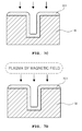
- FIGS. 7A to 7D are cross-sectional views illustrating an appearance in which the insulation layer according to the embodiment of the present invention is deposited on a trench that is formed in the surface of a substrate;
- FIGS. 8 to 10 are graphs which compares wet etch rates of oxide layers deposited on trenches, according to the embodiment of the present invention, depending on the frequency;
- FIG. 11 is a cross-sectional view illustrating a mode in which a plasma moves on the substrate.
- FIG. 12 is a graph illustrating ion energy according to the frequency of RF power applied during the formation of plasma.
- FIGS. 1 to 12 The present invention may, however, be embodied in different forms and should not be constructed as limited to the embodiments set forth herein. Rather, these embodiments are provided so that this disclosure will be thorough and complete, and will fully convey the scope of the present invention to those skilled in the art. Thus, the size of each element may be exaggerated for convenience in description and clarity.
- FIG. 1 is a flowchart illustrating a method of depositing an insulation layer according to an embodiment of the present invention.
- a substrate is loaded into a chamber of a semiconductor manufacturing apparatus (S 100 ).
- An insulation layer is deposited on the substrate loaded into the chamber (S 200 ), and the insulation layer deposition step S 200 includes a silicon layer forming step S 210 , a first purge step S 220 , a reaction step S 230 , and a second purge step S 240 .
- a silicon precursor may be injected into the chamber to allow silicon to be adsorbed on the substrate (S 210 ).
- the silicon layer is formed on the substrate, and the first purge step S 220 of removing the unreacted silicon precursor and reaction byproducts is then performed.
- the reaction step S 230 is performed in which the silicon layer formed on the substrate is reacted with a reaction source to form an insulation layer including silicon.
- a reaction source may be injected into the chamber.
- the first reaction source for example, may be at least one gas selected from the group consisting of O 2 , O 3 , N 2 , and NH 3 .
- the first reaction source may be a gas including oxygen atoms, such as O 2 or O 3 , or O 2 — (oxygen anion) or O* (oxygen radical) formed by using a plasma in an O 2 atmosphere.
- the first reaction source may be a gas including nitrogen atoms such as N 2 or NH 3 .
- the second purge step S 240 of removing reaction byproducts and the reaction source or ignition gas from the inside of the chamber may be performed.
- the silicon layer forming step S 210 , the first purge step S 220 , the reaction step S 230 , and the second purge step S 240 may be repeatedly performed (S 250 ).
- the silicon layer forming step S 210 , the first purge step S 220 , the reaction step S 230 , and the second purge step S 240 may be repeated 3 to 50 times.
- a temperature of the substrate and a pressure in the chamber may be constantly maintained.
- the silicon layer forming step S 210 at least one silicon atom layer may be formed on the substrate.
- the insulation layer including silicon may be formed to have a thickness of a few to a few tens of ⁇ .
- the insulation layer including silicon is formed and a densification step S 300 is then performed.
- a plasma atmosphere may be formed in the chamber to densify the insulation layer including silicon.
- a second reaction source may be further injected.
- the second reaction source may be at least one gas selected from the group consisting of H 2 , O 2 , O 3 , N 2 , and NH 3 .
- the insulation layer deposition step S 200 and the densification step S 300 may be repeatedly performed if necessary (S 400 ).
- the substrate may be unloaded from the chamber (S 900 ).
- FIG. 2 is a diagram illustrating the progress of the method of depositing an insulation layer according to the embodiment of the present invention.
- injection and purge of a silicon (Si) precursor and injection and purge of a first reaction source are repeatedly performed.
- the purge after the injection of the Si precursor and the purge after the injection of the first reaction source are repeatedly performed and a plasma atmosphere is then formed.
- a second reaction source may be injected if necessary.
- the insulation layer including silicon is formed by repeatedly performing the injection and purge of the silicon precursor and the injection and purge of the first reaction source, and the insulation layer including silicon is then plasma-treated by forming the plasma atmosphere.
- the insulation layer including silicon and having a desired thickness may be obtained by repeating all of the above-described processes.
- the injection and purge of the silicon precursor and the injection and purge of the first reaction source may not only be repeatedly performed, but the formation of the insulation layer including silicon and the plasma treatment may also be repeatedly performed.
- FIGS. 3A to 6B Based on the above description and referring to FIGS. 3A to 6B , the method of depositing an insulation layer according to the embodiment of the present invention will be described in detail step-by-step.
- reference numerals in FIGS. 1 and 2 may be used together if necessary.
- FIGS. 3A to 3C are cross-sectional views illustrating a step of forming a silicon layer according to an embodiment of the present invention.
- FIG. 3A is a cross-sectional view illustrating a step of injecting a silicon precursor according to an embodiment of the present invention.
- a silicon precursor 50 is injected into a chamber into which a substrate 100 is loaded.
- the substrate 100 may include a semiconductor substrate such as a silicon or compound semiconductor wafer.
- the substrate 100 may include a substrate material different from a semiconductor, for example, glass, metal, ceramic, or quartz.
- the silicon precursor 50 may be an amino-based silane, such as bisethylmethylaminosilane (BEMAS), bisdimethylaminosilane (BDMAS), bisdiethylaminosilane (BDEAS), tetrakisethylmethylaminosilane (TEMAS), tetrakisdimethylaminosilane (TDMAS), and tetrakisdiethylaminosilane (TDEAS), or a chloride-based silane such as hexachlorinedisilane (HCD).
- a temperature of the substrate 100 may be maintained in a range of 50° C. to 700° C. so as to allow the substrate 100 to react with the silicon precursor 50 .
- a pressure in the chamber into which the substrate 100 is loaded may be maintained in a range of 0.05 Torr to 10 Torr.
- FIG. 3B is a cross-sectional view illustrating an appearance in which a silicon layer is formed on the substrate according to the embodiment of the present invention.
- silicon is adsorbed on the substrate 100 by the reaction of a portion of the silicon precursor 50 with the substrate 50 and thus, a silicon layer 112 may be formed.
- the silicon layer 112 may be composed of at least one silicon atom layer.
- the silicon precursor 50 may form byproducts 52 after the reaction with the substrate 100 . Also, another portion of the silicon precursor 50 may not react with the substrate 100 and may remain in an unreacted state.
- FIG. 3C is a cross-sectional view illustrating an appearance in which a first purge step according to an embodiment of the present invention is performed.
- the silicon layer 112 is formed on the substrate 100 , and a purge for removing the remaining silicon precursor 50 in an unreacted state and the reaction byproducts 52 from the inside of the chamber may then be performed.
- a purge step in which the unreacted silicon precursor 50 and the reaction byproducts 52 are removed from the inside of the chamber, may be referred to as the first purge step.
- the temperature of the substrate 100 may be maintained in a range of 50° C. to 700° C.
- the pressure in the chamber into which the substrate 100 is loaded may be maintained in a range of 0.05 Torr to 10 Torr. That is, the temperature of the substrate 100 and the pressure in the chamber during the step of forming the silicon layer 112 and the first purge step may be constantly maintained.
- FIGS. 4A to 4C are cross-sectional views illustrating a step of forming an insulation layer including silicon according to an embodiment of the present invention.
- FIG. 4A is a cross-sectional view illustrating a step of injecting a reaction source according to an embodiment of the present invention.
- a first reaction source 60 is injected into a chamber into which a substrate 100 is loaded.
- the first reaction source 60 may be at least one gas selected from the group consisting of O 2 , O 3 , N 2 , and NH 3 .
- the first reaction source 60 for example, may be O 2 — (oxygen anion) or O* (oxygen radical) formed by using a plasma in an 02 atmosphere.
- a temperature of the substrate 100 may be maintained in a range of 50° C. to 700° C. so as to allow the substrate 100 to react with the first reaction source 60 . Also, a pressure in the chamber into which the substrate 100 is loaded may be maintained in a range of 0.05 Torr to 10 Torr.
- FIG. 4B is a cross-sectional view illustrating an appearance in which an insulation including silicon is deposited on the substrate according to the embodiment of the present invention.
- an insulation layer 122 a including silicon may be formed on the substrate 100 by the reaction of a portion of the first reaction source 60 with the silicon layer 112 .
- the first reaction source 60 may form reaction byproducts 62 after the reaction with the silicon layer 112 .
- another portion of the first reaction source 60 may not react with the silicon layer 112 and may remain in an unreacted state.
- the silicon layer 112 may be formed as a silicon oxide layer by reacting with the oxygen atoms included in the first reaction source 60 .
- a gas including nitrogen atoms such as N 2 or NH 3 , for example, is used as the first reaction source 60
- the silicon layer 112 may be formed as a silicon nitride layer by reacting with the nitrogen atoms included in the first reaction source 60 .
- FIG. 4C is a cross-sectional view illustrating an appearance in which a second purge step according to an embodiment of the present invention is performed.
- the insulation layer 122 a including silicon is formed on the substrate 100 and a purge for removing the remaining first reaction source 60 in an unreacted state and the reaction byproducts 62 from the inside of the chamber may then be performed.
- a purge step in which the unreacted first reaction source 60 and the reaction byproducts 62 are removed from the inside of the chamber, may be referred to as the second purge step.
- the temperature of the substrate 100 may be maintained in a range of 50° C. to 700° C.
- the pressure in the chamber into which the substrate 100 is loaded may be maintained in a range of 0.05 Torr to 10 Torr.
- FIG. 5 is a cross-sectional view illustrating an appearance in which a plurality of insulation layers including silicon according to an embodiment of the present invention is formed.
- an insulation layer 122 composed of a plurality of insulation layers 122 a , 122 b , and 122 c including silicon is formed by repeating the steps illustrated in FIGS. 3A to 4C .
- the insulation layer 122 may have a thickness of a few to a few tens of A.
- the process of depositing each insulation layer 122 a , 122 b , or 122 c including silicon may be repeated 3 to 50 times so as to allow the insulation layer 122 to include 3 to 10 insulation layers 122 a , 122 b , and 122 c including silicon.
- the insulation layer 122 may have excellent quality and step coverage.
- FIGS. 6A and 6B are cross-sectional views illustrating a step of densifying the insulation layer according to the embodiment of the present invention.
- FIG. 6 is a cross-sectional view illustrating an appearance in which a plasma atmosphere is provided to the insulation layer including silicon according to the embodiment of the present invention.
- a plasma is applied to the substrate 100 having the insulation layer 122 formed thereon. That is, a plasma atmosphere is formed in the chamber into which the substrate 100 is loaded.
- a capacitively coupled plasma (CCP) method may be used to form the plasma atmosphere, and a CCP electrode (e.g., round or square) is connected to a radio frequency (RF) power source through a matcher.
- the RF power source may have a frequency of 400 kHz to 2 MHz and an output power of 100 W to 3 kW. The output power may be adjusted to be proportional to the frequency of the RF power source.
- At least one ignition gas selected from the group consisting of argon (Ar), helium (He), krypton (Kr), and xenon (Xe), for example, may be injected to form the plasma atmosphere.
- the ignition gas may be injected at a flow rate of 50 sccm to 3,000 sccm.
- a second reaction source 64 may be further injected to more densify the insulation layer 122 in the plasma atmosphere.
- the second reaction source 64 may be at least one gas selected from the group consisting of O 2 , O 3 , N 2 , and NH 3 , or O 2 — (oxygen anion) or O* (oxygen radical) formed by using a plasma in an O 2 atmosphere.
- the insulation layer 122 is a silicon oxide layer
- a gas including oxygen atoms such as O 2 or O 3 , O 2 — (oxygen anion) or O* (oxygen radical) formed by using a plasma in an O 2 atmosphere, or H 2 , for example, may be used as the second reaction source 64 .
- a gas including nitrogen atoms such as N 2 or NH 3 , for example, may be used as the second reaction source 64 .
- FIG. 6B is a cross-sectional view illustrating an appearance in which an insulation layer 122 D according to an embodiment of the present invention is formed.
- the densification of the insulation layer 122 is performed in the plasma atmosphere and thus, the densified insulation layer 122 D may be formed.
- the pressure of the chamber into which the substrate 100 is loaded may be maintained in a range of 0.05 Torr to 10 Torr to form the densified insulation layer 122 D.
- the densified insulation layer 122 D obtained by treating the insulation layer 122 in the plasma atmosphere may have excellent quality such as insulating properties.
- the densified insulation layer 122 D may have excellent quality even if the densified insulation layer 122 D is formed to have a small thickness.
- the thin film has a higher etch rate than a thermal oxide layer (oxide layer obtained by an oxidation treatment while heating a silicon substrate).
- ALD atomic layer deposition
- the silicon oxide layer deposited by the ALD method has a lower density than the thermal oxide layer.
- the density of the thin film may be improved by the above-described densification treatment.
- FIGS. 7A to 7D are cross-sectional views illustrating an appearance in which the insulation layer according to the embodiment of the present invention is deposited on a trench that is formed in the surface of a substrate, and the above-described method of depositing an insulation layer may be used.
- the trench may have a depth of 300 nm to 10 ⁇ m and a width of 10 nm to 200 nm.
- a component of a silicon precursor is adsorbed on the surface of the substrate W to form a silicon adsorption layer 300 (see FIG. 7B ), and thereafter, the adsorption layer 300 is oxidized or nitrided by the first reaction source 60 to form a single molecular layer or multiple molecular layers of a silicon oxide layer or silicon nitride layer as a component of a thin film.
- an insulation layer 301 is formed (see FIG. 7C ).
- impurities such as moisture (OH group) or an organic material, may remain due to a residual group included in the silicon precursor.
- high-frequency power is supplied by a RF power source to form an electric field and a magnetic field
- the ignition gas or the second reaction source 64 is activated by the magnetic field to form a plasma containing, for example, ions or radicals. Since the plasma collides against the surface of the substrate W, the impurities, such as moisture or an organic material, may be released from the insulation layer 301 or elements in the insulation layer 301 may be rearranged to densify the insulation layer 301 .
- a degree of densification may change in a depth direction of the trench 10 . That is, in a case in which the trench 10 having a high aspect ratio is formed, it is difficult for the plasma (or ions) to enter into the trench. Thus, in the trench 10 , the degree of densification decreases in a direction toward the bottom. In other words, the densification treatment is well performed on the surface of the insulation layer 301 and the bottom of the trench 10 to form a dense thin film, but a low density (porous) thin film is obtained in the direction toward the bottom of the trench 10 . Thus, there is a need to form a dense thin film along the depth direction of the trench 10 .
- FIGS. 8 to 10 are graphs which compares wet etch rates of the oxide layers deposited on the trenches, according to the embodiment of the present invention, depending on the frequency, wherein the wet etch rate is represented as a ratio to a wet etch rate of the above-described thermal oxide layer.
- FIG. 8 illustrates the wet etch rate of the oxide layer depending on the frequency of the RF power source along the depth of the trench 10 when the aspect ratio of the trench 10 is 10:1.
- the differences in wet etch rates depending on the frequency are clearly observed at points where the aspect ratios are 5:1 and 10:1, and since the densification treatment is not performed in a case in which the frequency is 13.56 MHz, it may be understood that the density of the insulation layer is low. That is, at the points where the aspects ratios are 5:1 and 10:1, in a case in which the frequency of the RF power source is a widely used frequency, i.e., 13.56 MHz, the wet etch rates are about 4.8 times higher (worse) than those of the thermal oxide layers. However, in a case in which the frequency of the RF power source is 2 MHz, it may be understood that the wet etch rates are about 2.4 to 5 times higher (worse) than those of the thermal oxide layers.
- FIG. 9 illustrates the wet etch rate of the oxide layer depending on the frequency of the RF power source along the depth of the trench 10 when the aspect ratio of the trench 10 is 30:1.
- the differences in wet etch rates depending on the frequency are clearly observed at points where the aspect ratios are in a range of 5:1 to 30:1, and since the densification treatment is not performed in a case in which the frequency is 13.56 MHz, it may be understood that the density of the insulation layer is low. That is, at the points where the aspects ratios are in a range of 5:1 to 30:1, in a case in which the frequency of the RF power source is a widely used frequency, i.e., 13.56 MHz, the wet etch rates are about 4.2 to 9 times higher (worse) than those of the thermal oxide layers. However, in a case in which the frequency of the RF power source is 2 MHz, it may be understood that the wet etch rates are about 2.4 to 3.1 times higher (worse) than those of the thermal oxide layers.
- FIG. 10 illustrates the wet etch rate of the oxide layer along the depth of the trench 10 when the aspect ratio of the trench 10 is 30:1 and the frequency of the RF power source is 380 kHz.
- the frequency of the RF power source is 380 kHz, i.e., less than 2 MHz
- the densification treatment is performed so that the insulation layer is densified.
- the differences in wet etch rates depending on the frequency are clearly observed at points excluding the bottom of the trench 10 , and, different from the description of FIG.
- the densification treatment is not performed even at the surface (point where the depth is 0) of the oxide layer and a point where the aspect ratio is 2:1 (inner wall of a point where the depth from the surface is 2 when the depth of the trench is 30), it may be understood that the density of the insulation layer is low.
- FIG. 11 is a cross-sectional view illustrating a mode in which a plasma moves on the substrate
- FIG. 12 is a graph illustrating ion energy according to the frequency of RF power applied during the formation of plasma. The presence of the densification treatment described through FIGS. 8 to 10 will be described below.
- the plasma collides against the surface of the substrate W, impurities, such as moisture or an organic material, may be released from the oxide layer or elements in the insulation layer 301 may be rearranged to densify the oxide layer.
- the trench 10 such as a hole or groove, having a high aspect ratio (e.g., 5:1 or more) is formed in the surface of the substrate, a degree of densification may change in a depth direction of the trench 10 . That is, in a case in which the trench 10 having a high aspect ratio is formed, it is difficult for the plasma (or ions) to enter into the trench.
- the degree of densification decreases in a direction toward the bottom.
- the densification treatment is well performed on the surface of the insulation layer 301 and the bottom of the trench 10 to form a dense thin film, but a low density (porous) thin film is obtained in the direction toward the bottom of the trench 10 .
- a dense thin film along the depth direction of the trench 10 .
- the above-described phenomenon is considered to occur due to the linearity of the plasma. That is, since a movement direction of the plasma is parallel to the inner wall of the trench 10 , the possibility of the plasma colliding with the inner wall of the trench 10 is low. Also, since the bottom of the trench 10 is perpendicular to the movement direction of the plasma, the bottom of the trench 10 may sufficiently collide with the plasma to absorb a significant amount of impact energy. In contrast, since the inner wall of the trench 10 is generally parallel to the movement direction of the plasma, the inner wall of the trench may not sufficiently collide with the plasma even if the plasma collides with the inner wall of the trench and may not absorb a significant amount of impact energy (see FIG. 11( a ) )
- the ions may sufficiently collide with the inner wall of the trench 10 so that the inner wall of the trench 10 may absorb a significant amount of impact energy (see FIG. 11( b ) ).
- the ions may lose a significant amount of energy during the collision between the ions and the neutral atoms, the ions may not have a sufficient energy to induce the densification even if the ions change their directions to collide with the inner wall of the trench 10 as described above. Therefore, the ions of the initially formed plasma may induce the densification of the inner wall of the trench 10 only when the energy of the ions is above a predetermined level.
- the output power of the RF power source may be in a range of 100 W to 3 kW, and the output power may be adjusted to be proportional to the frequency of the RF power source. Since the ions having high energy are distributed as the frequency decreases, a sputtering effect may significantly occur at edge portions of the entrance of the trench 10 when the output power of the RF power source is increased, and thus, the shape of the trench 10 may be damaged or distorted. Therefore, there is a need to adjust the output power of the RF power source to be proportional to the frequency.
- an inductively coupled plasma may be used alternatively.
- the present invention may be applicable to a various apparatus for manufacturing semiconductor or a various method for manufacturing semiconductor.
Abstract
Provided is a method of depositing an insulation layer on a trench in a substrate, in which the trench having an aspect ratio of 5:1 or more is formed, including: an insulation layer deposition step of performing an adsorption step of adsorbing silicon to the substrate by injecting a silicon precursor into the inside of a chamber into which the substrate is loaded, a first purge step of removing the unreacted silicon precursor and reaction byproducts from the inside of the chamber, a reaction step of forming the adsorbed silicon as an insulation layer including silicon by supplying a first reaction source to the inside of the chamber, and a second purge step of removing the unreacted first reaction source and reaction byproducts from the inside of the chamber; and a densification step of forming a plasma atmosphere in the inside of the chamber by applying an radio frequency (RF) power and densifying the insulation layer including silicon by using the plasma atmosphere, wherein a frequency of the RF power is in a range of 400 kHz to 2 MHz.
Description
The present invention disclosed herein relates to methods of depositing an insulation layer, and more particularly, to methods of depositing an insulation layer on a trench having a high aspect ratio.
In line with the recent development of semiconductor industry and requirements of users, electronic devices have been highly integrated with high performance, and accordingly, high integration and high performance of a semiconductor device, as a key component of electronic devices, have been also required. However, there are difficulties in realizing a microstructure for obtaining a highly integrated semiconductor device.
For example, a thinner insulation layer is required for realizing the microstructure. However, when the insulation layer is formed to have a smaller thickness, qualities of the layer, such as insulating properties, may deteriorate. In particular, it becomes difficult to form a uniform, high quality insulation layer on an entire trench having a high aspect ratio while decreasing the thickness of the thin film.
The present invention provides a method capable of depositing an insulation layer having excellent quality and step coverage.
The present invention also provides a method capable of depositing a high quality insulation layer in a thickness direction of a trench even in a case in which the trench having a high aspect ratio is formed in the surface of a substrate.
These and other objects of the present invention will be more apparent from the following detailed description and the accompanying drawings.
Embodiments of the present invention provide methods of depositing an insulation layer on a trench in a substrate, in which the trench having an aspect ratio of 5:1 or more is formed, including: an insulation layer deposition step of performing an adsorption step of adsorbing silicon to the substrate by injecting a silicon precursor into the inside of a chamber into which the substrate is loaded, a first purge step of removing the unreacted silicon precursor and reaction byproducts from the inside of the chamber, a reaction step of forming the adsorbed silicon as an insulation layer including silicon by supplying a first reaction source to the inside of the chamber, and a second purge step of removing the unreacted first reaction source and reaction byproducts from the inside of the chamber; and a densification step of forming a plasma atmosphere in the inside of the chamber by applying an radio frequency (RF) power and densifying the insulation layer including silicon by using the plasma atmosphere, wherein a frequency of the RF power is in a range of 400 kHz to 2 MHz.
In some embodiments, the densification step may be performed for 10 seconds when the insulation layer has a thickness of 50 Å.
In other embodiments, an output of the RF power may be in a range of 100 W to 3 kW, and the output of the RF power may be adjusted to be proportional to the frequency of the RF power.
In still other embodiments, the plasma atmosphere may be formed by a capacitively coupled plasma (CCP) method.
In even other embodiments, the first reaction source may be at least one gas selected from the group consisting of O2, O3, N2, and NH3.
In yet other embodiments, in the densification step, the plasma atmosphere may be formed by injecting at least one ignition gas selected from the group consisting of argon (Ar), helium (He), krypton (Kr), and xenon (Xe).
In further embodiments, in the densification step, at least one second reaction source selected from the group consisting of H2, O2, O3, N2, and NH3 may be further injected with the ignition gas.
In still further embodiments, in the reaction step, O2— (oxygen anion) or O* (oxygen radical) formed by using a plasma in an O2 atmosphere may be used as the first reaction source.
In even further embodiments, in the insulation layer deposition step, an internal pressure of the chamber may be in a range of 0.05 Torr to 10 Torr, and an internal temperature of the chamber may be in a range of 50° C. to 700° C.
In yet further embodiments, the adsorption step, the first purge step, the reaction step, and the second purge step may be repeated 3 to 50 times before the densification step.
In much further embodiments, the insulation deposition step and the plasma treatment step may be repeated.
In still much further embodiments, a wet etch rate, based on using a 300:1 buffered oxide etchant (BOE) for 150 seconds, of the insulation layer subjected to the densification step may be 4 times or less that of an insulation layer by thermal chemical vapor deposition (CVD).
According to an embodiment of the present invention, an insulation layer having excellent quality and step coverage may be formed. In particular, a high quality insulation layer may be deposited in a thickness direction of a trench even in a case in which the trench having a high aspect ratio is formed in the surface of a substrate.
Hereinafter, preferred examples of the present invention will be described in more detail with reference to the accompanying FIGS. 1 to 12 . The present invention may, however, be embodied in different forms and should not be constructed as limited to the embodiments set forth herein. Rather, these embodiments are provided so that this disclosure will be thorough and complete, and will fully convey the scope of the present invention to those skilled in the art. Thus, the size of each element may be exaggerated for convenience in description and clarity.
In order to form the silicon layer, a silicon precursor may be injected into the chamber to allow silicon to be adsorbed on the substrate (S210). The silicon layer is formed on the substrate, and the first purge step S220 of removing the unreacted silicon precursor and reaction byproducts is then performed.
Thereafter, the reaction step S230 is performed in which the silicon layer formed on the substrate is reacted with a reaction source to form an insulation layer including silicon. In order to form the silicon layer as the insulation layer including silicon, a first reaction source may be injected into the chamber. The first reaction source, for example, may be at least one gas selected from the group consisting of O2, O3, N2, and NH3.
In a case in which the insulation layer including silicon is a silicon oxide layer, the first reaction source may be a gas including oxygen atoms, such as O2 or O3, or O2— (oxygen anion) or O* (oxygen radical) formed by using a plasma in an O2 atmosphere. In a case in which the insulation layer including silicon is a silicon nitride layer, the first reaction source may be a gas including nitrogen atoms such as N2 or NH3.
Thereafter, the second purge step S240 of removing reaction byproducts and the reaction source or ignition gas from the inside of the chamber may be performed.
The silicon layer forming step S210, the first purge step S220, the reaction step S230, and the second purge step S240 may be repeatedly performed (S250). The silicon layer forming step S210, the first purge step S220, the reaction step S230, and the second purge step S240, for example, may be repeated 3 to 50 times.
During the insulation layer deposition step S200 including the silicon layer forming step S210, the first purge step S220, the reaction step S230, and the second purge step S240, a temperature of the substrate and a pressure in the chamber may be constantly maintained. In the silicon layer forming step S210, at least one silicon atom layer may be formed on the substrate. For example, the insulation layer including silicon may be formed to have a thickness of a few to a few tens of Å. The insulation layer including silicon is formed and a densification step S300 is then performed.
A plasma atmosphere may be formed in the chamber to densify the insulation layer including silicon. Also, together with the plasma atmosphere, a second reaction source may be further injected. The second reaction source, for example, may be at least one gas selected from the group consisting of H2, O2, O3, N2, and NH3. In order to obtain an insulation layer including silicon and having a desired thickness, the insulation layer deposition step S200 and the densification step S300 may be repeatedly performed if necessary (S400). In a case in which the insulation layer including silicon and having a desired thickness is formed, the substrate may be unloaded from the chamber (S900).
From the step, in which the injection and purge of the silicon precursor and the injection and purge of the first reaction source are repeatedly performed, to the step of forming the plasma atmosphere is performed as one cycle. That is, the insulation layer including silicon is formed by repeatedly performing the injection and purge of the silicon precursor and the injection and purge of the first reaction source, and the insulation layer including silicon is then plasma-treated by forming the plasma atmosphere. Also, the insulation layer including silicon and having a desired thickness may be obtained by repeating all of the above-described processes. Thus, in the method of depositing an insulation layer, the injection and purge of the silicon precursor and the injection and purge of the first reaction source may not only be repeatedly performed, but the formation of the insulation layer including silicon and the plasma treatment may also be repeatedly performed.
Based on the above description and referring to FIGS. 3A to 6B , the method of depositing an insulation layer according to the embodiment of the present invention will be described in detail step-by-step. In descriptions related to FIGS. 3A to 6B , reference numerals in FIGS. 1 and 2 may be used together if necessary.
Referring to FIG. 3A , a silicon precursor 50 is injected into a chamber into which a substrate 100 is loaded. The substrate 100, for example, may include a semiconductor substrate such as a silicon or compound semiconductor wafer. Also, the substrate 100 may include a substrate material different from a semiconductor, for example, glass, metal, ceramic, or quartz. The silicon precursor 50, for example, may be an amino-based silane, such as bisethylmethylaminosilane (BEMAS), bisdimethylaminosilane (BDMAS), bisdiethylaminosilane (BDEAS), tetrakisethylmethylaminosilane (TEMAS), tetrakisdimethylaminosilane (TDMAS), and tetrakisdiethylaminosilane (TDEAS), or a chloride-based silane such as hexachlorinedisilane (HCD). A temperature of the substrate 100 may be maintained in a range of 50° C. to 700° C. so as to allow the substrate 100 to react with the silicon precursor 50. Also, a pressure in the chamber into which the substrate 100 is loaded may be maintained in a range of 0.05 Torr to 10 Torr.
In a case in which a gas including oxygen atoms, such as O2 or O3, or O2— (oxygen anion) or O* (oxygen radical) formed by using a plasma in an O2 atmosphere, for example, is used as the first reaction source 60, the silicon layer 112 may be formed as a silicon oxide layer by reacting with the oxygen atoms included in the first reaction source 60. In a case in which a gas including nitrogen atoms, such as N2 or NH3, for example, is used as the first reaction source 60, the silicon layer 112 may be formed as a silicon nitride layer by reacting with the nitrogen atoms included in the first reaction source 60.
At least one ignition gas selected from the group consisting of argon (Ar), helium (He), krypton (Kr), and xenon (Xe), for example, may be injected to form the plasma atmosphere. In this case, the ignition gas may be injected at a flow rate of 50 sccm to 3,000 sccm. A second reaction source 64 may be further injected to more densify the insulation layer 122 in the plasma atmosphere. The second reaction source 64, for example, may be at least one gas selected from the group consisting of O2, O3, N2, and NH3, or O2— (oxygen anion) or O* (oxygen radical) formed by using a plasma in an O2 atmosphere.
In a case in which the insulation layer 122 is a silicon oxide layer, a gas including oxygen atoms, such as O2 or O3, O2— (oxygen anion) or O* (oxygen radical) formed by using a plasma in an O2 atmosphere, or H2, for example, may be used as the second reaction source 64. In a case in which the insulation layer 122 is a silicon nitride layer, a gas including nitrogen atoms, such as N2 or NH3, for example, may be used as the second reaction source 64.
For example, in a case where an oxidation layer is deposited by using an atomic layer deposition (ALD) method at a relatively low temperature of about 300° C. to about 650° C., the thin film has a higher etch rate than a thermal oxide layer (oxide layer obtained by an oxidation treatment while heating a silicon substrate). Thus, it may be considered that the silicon oxide layer deposited by the ALD method has a lower density than the thermal oxide layer. The density of the thin film may be improved by the above-described densification treatment.
That is, a trench 10 composed of a groove or hole is formed in a surface of a substrate W, and the trench 10 has an aspect ratio (AR=a height h of the trench:a width w of the trench) (see FIG. 7a ). For example, the trench may have a depth of 300 nm to 10 μm and a width of 10 nm to 200 nm.
A component of a silicon precursor is adsorbed on the surface of the substrate W to form a silicon adsorption layer 300 (see FIG. 7B ), and thereafter, the adsorption layer 300 is oxidized or nitrided by the first reaction source 60 to form a single molecular layer or multiple molecular layers of a silicon oxide layer or silicon nitride layer as a component of a thin film. Thus, an insulation layer 301, as a reaction product, is formed (see FIG. 7C ). In the insulation layer 301, for example, there is a case in which impurities, such as moisture (OH group) or an organic material, may remain due to a residual group included in the silicon precursor.
Thereafter, high-frequency power is supplied by a RF power source to form an electric field and a magnetic field, and the ignition gas or the second reaction source 64 is activated by the magnetic field to form a plasma containing, for example, ions or radicals. Since the plasma collides against the surface of the substrate W, the impurities, such as moisture or an organic material, may be released from the insulation layer 301 or elements in the insulation layer 301 may be rearranged to densify the insulation layer 301.
However, in a case in which the trench 10, such as a hole or groove, having a high aspect ratio (e.g., 5:1 or more) is formed in the surface of the substrate, a degree of densification may change in a depth direction of the trench 10. That is, in a case in which the trench 10 having a high aspect ratio is formed, it is difficult for the plasma (or ions) to enter into the trench. Thus, in the trench 10, the degree of densification decreases in a direction toward the bottom. In other words, the densification treatment is well performed on the surface of the insulation layer 301 and the bottom of the trench 10 to form a dense thin film, but a low density (porous) thin film is obtained in the direction toward the bottom of the trench 10. Thus, there is a need to form a dense thin film along the depth direction of the trench 10.
As described above, since the plasma collides against the surface of the substrate W, impurities, such as moisture or an organic material, may be released from the oxide layer or elements in the insulation layer 301 may be rearranged to densify the oxide layer. However, in a case in which the trench 10, such as a hole or groove, having a high aspect ratio (e.g., 5:1 or more) is formed in the surface of the substrate, a degree of densification may change in a depth direction of the trench 10. That is, in a case in which the trench 10 having a high aspect ratio is formed, it is difficult for the plasma (or ions) to enter into the trench. Thus, in the trench 10, the degree of densification decreases in a direction toward the bottom. In other words, the densification treatment is well performed on the surface of the insulation layer 301 and the bottom of the trench 10 to form a dense thin film, but a low density (porous) thin film is obtained in the direction toward the bottom of the trench 10. Thus, there is a need to form a dense thin film along the depth direction of the trench 10.
The above-described phenomenon is considered to occur due to the linearity of the plasma. That is, since a movement direction of the plasma is parallel to the inner wall of the trench 10, the possibility of the plasma colliding with the inner wall of the trench 10 is low. Also, since the bottom of the trench 10 is perpendicular to the movement direction of the plasma, the bottom of the trench 10 may sufficiently collide with the plasma to absorb a significant amount of impact energy. In contrast, since the inner wall of the trench 10 is generally parallel to the movement direction of the plasma, the inner wall of the trench may not sufficiently collide with the plasma even if the plasma collides with the inner wall of the trench and may not absorb a significant amount of impact energy (see FIG. 11(a) )
Thus, only when ions included in the plasma collide at least once with neutral atoms to considerably change their directions, the ions may sufficiently collide with the inner wall of the trench 10 so that the inner wall of the trench 10 may absorb a significant amount of impact energy (see FIG. 11(b) ). However, since the ions may lose a significant amount of energy during the collision between the ions and the neutral atoms, the ions may not have a sufficient energy to induce the densification even if the ions change their directions to collide with the inner wall of the trench 10 as described above. Therefore, the ions of the initially formed plasma may induce the densification of the inner wall of the trench 10 only when the energy of the ions is above a predetermined level.
As illustrated in FIG. 12 , the smaller the frequency of the RF power is, the wider the distribution of the ion energy is and ions having higher energy are distributed. Accordingly, ions having relatively high energy may collide with the inner wall of the trench 10 to induce the densification. However, when the frequency is excessively low, since the number of ions may be decreased even if the ions having higher energy are formed, the densification of the oxide layer may not be induced. Thus, the frequency of the RF power may be in a range of 400 kHz to 2 MHz, and as illustrated in FIGS. 8 to 10 , the density of the oxide layer may be improved by densifying the inner wall of the trench 10.
The output power of the RF power source may be in a range of 100 W to 3 kW, and the output power may be adjusted to be proportional to the frequency of the RF power source. Since the ions having high energy are distributed as the frequency decreases, a sputtering effect may significantly occur at edge portions of the entrance of the trench 10 when the output power of the RF power source is increased, and thus, the shape of the trench 10 may be damaged or distorted. Therefore, there is a need to adjust the output power of the RF power source to be proportional to the frequency.
Although the CCP is used in the present embodiment, an inductively coupled plasma (ICP) may be used alternatively.
While preferred embodiments of the present invention has been particularly shown and described with reference to the accompanying drawings, it will be understood by those of ordinary skill in the art that various changes in form and details may be made therein without departing from the spirit and scope of the present invention as defined by the following claims. Accordingly, it is to be understood that the invention is not to be limited by the disclosed embodiments, but only by the scope of the appended claims.
The present invention may be applicable to a various apparatus for manufacturing semiconductor or a various method for manufacturing semiconductor.
Claims (16)
1. A method of depositing an insulation layer on a trench in a substrate in which the trench having an aspect ratio of 5:1 or more is formed, the method comprising:
an insulation layer deposition step of performing
an adsorption step of adsorbing silicon to the substrate by injecting a silicon precursor into an inside of a chamber into which the substrate is loaded,
a first purge step of removing the unreacted silicon precursor and reaction byproducts from the inside of the chamber,
a reaction step of forming the adsorbed silicon as an insulation layer including silicon by supplying a first reaction source to the inside of the chamber, and
a second purge step of removing the unreacted first reaction source and reaction byproducts from the inside of the chamber; and
a densification step of forming a plasma atmosphere in the inside of the chamber by applying a radio frequency (RF) power and densifying the insulation layer including silicon by using the plasma atmosphere,
wherein a frequency of the RF power in the densification step is 2 MHz.
2. The method of claim 1 , wherein a wet etch rate, based on using a 300:1 buffered oxide etchant (BOE) for 150 seconds, of the insulation layer subjected to the densification step is 4 times or less that of an insulation layer by thermal chemical vapor deposition (CVD).
3. The method of claim 1 , wherein the densification step is performed for 2 seconds to 50 seconds when the insulation layer has a thickness of 50 Å.
4. The method of claim 3 , wherein a wet etch rate, based on using a 300:1 buffered oxide etchant (BOE) for 150 seconds, of the insulation layer subjected to the densification step is 4 times or less that of an insulation layer by thermal chemical vapor deposition (CVD).
5. The method of claim 1 , wherein an output of the RF power is in a range of 100 W to 3 kW, and
the output of the RF power is adjusted to be proportional to the frequency of the RF power.
6. The method of claim 5 , wherein a wet etch rate, based on using a 300:1 buffered oxide etchant (BOE) for 150 seconds, of the insulation layer subjected to the densification step is 4 times or less that of an insulation layer by thermal chemical vapor deposition (CVD).
7. The method of claim 1 , wherein the plasma atmosphere is formed by a capacitively coupled plasma (CCP) method.
8. The method of claim 7 , wherein a wet etch rate, based on using a 300:1 buffered oxide etchant (BOE) for 150 seconds, of the insulation layer subjected to the densification step is 4 times or less that of an insulation layer by thermal chemical vapor deposition (CVD).
9. The method of claim 1 , wherein the first reaction source is at least one gas selected from the group consisting of O2, O3, N2, and NH3.
10. The method of claim 9 , wherein a wet etch rate, based on using a 300:1 buffered oxide etchant (BOE) for 150 seconds, of the insulation layer subjected to the densification step is 4 times or less that of an insulation layer by thermal chemical vapor deposition (CVD).
11. The method of claim 1 , wherein, in the densification step, the plasma atmosphere is formed by injecting at least one ignition gas selected from the group consisting of argon (Ar), helium (He), krypton (Kr), and xenon (Xe).
12. The method of claim 11 , wherein a wet etch rate, based on using a 300:1 buffered oxide etchant (BOE) for 150 seconds, of the insulation layer subjected to the densification step is 4 times or less that of an insulation layer by thermal chemical vapor deposition (CVD).
13. The method of claim 11 , wherein, in the densification step, at least one second reaction source selected from the group consisting of H2, O2, O3, N2, and NH3 is further injected with the ignition gas.
14. The method of claim 13 , wherein a wet etch rate, based on using a 300:1 buffered oxide etchant (BOE) for 150 seconds, of the insulation layer subjected to the densification step is 4 times or less that of an insulation layer by thermal chemical vapor deposition (CVD).
15. The method of claim 1 , wherein, in the reaction step, O2— (oxygen anion) or O* (oxygen radical) formed by using a plasma in an O2 atmosphere is used as the first reaction source.
16. The method of claim 15 , wherein a wet etch rate, based on using a 300:1 buffered oxide etchant (BOE) for 150 seconds, of the insulation layer subjected to the densification step is 4 times or less that of an insulation layer by thermal chemical vapor deposition (CVD).
Applications Claiming Priority (3)
| Application Number | Priority Date | Filing Date | Title |
|---|---|---|---|
| KR1020140089285A KR101576637B1 (en) | 2014-07-15 | 2014-07-15 | Method for depositing on deep trehcn having high aspect ratio |
| KR10-2014-0089285 | 2014-07-15 | ||
| PCT/KR2015/006055 WO2016010267A1 (en) | 2014-07-15 | 2015-06-16 | Method for depositing insulating film on recessed portion having high aspect ratio |
Publications (2)
| Publication Number | Publication Date |
|---|---|
| US20170148625A1 US20170148625A1 (en) | 2017-05-25 |
| US9818604B2 true US9818604B2 (en) | 2017-11-14 |
Family
ID=54979289
Family Applications (1)
| Application Number | Title | Priority Date | Filing Date |
|---|---|---|---|
| US15/323,295 Active US9818604B2 (en) | 2014-07-15 | 2015-06-16 | Method for depositing insulating film on recessed portion having high aspect ratio |
Country Status (6)
| Country | Link |
|---|---|
| US (1) | US9818604B2 (en) |
| JP (1) | JP6371462B2 (en) |
| KR (1) | KR101576637B1 (en) |
| CN (1) | CN106489190B (en) |
| TW (1) | TWI575603B (en) |
| WO (1) | WO2016010267A1 (en) |
Cited By (1)
| Publication number | Priority date | Publication date | Assignee | Title |
|---|---|---|---|---|
| US11798834B2 (en) | 2019-02-20 | 2023-10-24 | Asm Ip Holding B.V. | Cyclical deposition method and apparatus for filling a recess formed within a substrate surface |
Families Citing this family (9)
| Publication number | Priority date | Publication date | Assignee | Title |
|---|---|---|---|---|
| KR102362534B1 (en) * | 2014-12-08 | 2022-02-15 | 주성엔지니어링(주) | Substrate disposition method |
| KR101960763B1 (en) * | 2016-11-03 | 2019-03-21 | 주식회사 유진테크 | Method for manufacturing an epitaxial layer in low temperature |
| JP6767885B2 (en) * | 2017-01-18 | 2020-10-14 | 東京エレクトロン株式会社 | Protective film forming method |
| JP6778144B2 (en) * | 2017-04-25 | 2020-10-28 | 株式会社Kokusai Electric | Semiconductor device manufacturing methods, substrate processing devices and programs |
| JP6903040B2 (en) * | 2018-09-21 | 2021-07-14 | 株式会社Kokusai Electric | Semiconductor device manufacturing methods, substrate processing devices, and programs |
| JP2021143360A (en) * | 2020-03-10 | 2021-09-24 | 株式会社昭和真空 | Vapor deposition source unit, vapor deposition source and vapor deposition source nozzle |
| JP7222946B2 (en) * | 2020-03-24 | 2023-02-15 | 株式会社Kokusai Electric | Semiconductor device manufacturing method, substrate processing apparatus, and program |
| US20220298636A1 (en) * | 2021-03-22 | 2022-09-22 | Applied Materials, Inc. | Methods and apparatus for processing a substrate |
| WO2024006211A1 (en) * | 2022-06-27 | 2024-01-04 | Lam Research Corporation | Deposition and etch of silicon-containing layer |
Citations (5)
| Publication number | Priority date | Publication date | Assignee | Title |
|---|---|---|---|---|
| JPH0729897A (en) | 1993-06-25 | 1995-01-31 | Nec Corp | Manufacture of semiconductor device |
| KR20070028858A (en) | 2005-09-08 | 2007-03-13 | 주식회사 아이피에스 | A method for depositing nitride thin film on wafer by in-situ |
| KR20120012582A (en) | 2010-08-02 | 2012-02-10 | 주식회사 유진테크 | Method of cyclic deposition thin film |
| US8912101B2 (en) * | 2012-03-15 | 2014-12-16 | Asm Ip Holding B.V. | Method for forming Si-containing film using two precursors by ALD |
| US20150235844A1 (en) * | 2014-02-18 | 2015-08-20 | Applied Materials, Inc. | Hermetic cvd-cap with improved step coverage in high aspect ratio structures |
Family Cites Families (9)
| Publication number | Priority date | Publication date | Assignee | Title |
|---|---|---|---|---|
| JPS556291B1 (en) * | 1969-11-26 | 1980-02-15 | ||
| JPS4825480A (en) * | 1971-08-04 | 1973-04-03 | ||
| WO1992012535A1 (en) * | 1991-01-08 | 1992-07-23 | Fujitsu Limited | Process for forming silicon oxide film |
| US8291857B2 (en) * | 2008-07-03 | 2012-10-23 | Applied Materials, Inc. | Apparatuses and methods for atomic layer deposition |
| US8563095B2 (en) * | 2010-03-15 | 2013-10-22 | Applied Materials, Inc. | Silicon nitride passivation layer for covering high aspect ratio features |
| JP2012079762A (en) * | 2010-09-30 | 2012-04-19 | Mitsubishi Heavy Ind Ltd | Insulation film forming apparatus and formation method |
| US8846536B2 (en) * | 2012-03-05 | 2014-09-30 | Novellus Systems, Inc. | Flowable oxide film with tunable wet etch rate |
| JP6040609B2 (en) * | 2012-07-20 | 2016-12-07 | 東京エレクトロン株式会社 | Film forming apparatus and film forming method |
| US9875888B2 (en) * | 2014-10-03 | 2018-01-23 | Applied Materials, Inc. | High temperature silicon oxide atomic layer deposition technology |
-
2014
- 2014-07-15 KR KR1020140089285A patent/KR101576637B1/en active IP Right Grant
-
2015
- 2015-06-16 US US15/323,295 patent/US9818604B2/en active Active
- 2015-06-16 CN CN201580037489.2A patent/CN106489190B/en active Active
- 2015-06-16 JP JP2017500342A patent/JP6371462B2/en active Active
- 2015-06-16 WO PCT/KR2015/006055 patent/WO2016010267A1/en active Application Filing
- 2015-07-03 TW TW104121630A patent/TWI575603B/en active
Patent Citations (7)
| Publication number | Priority date | Publication date | Assignee | Title |
|---|---|---|---|---|
| JPH0729897A (en) | 1993-06-25 | 1995-01-31 | Nec Corp | Manufacture of semiconductor device |
| US5521126A (en) | 1993-06-25 | 1996-05-28 | Nec Corporation | Method of fabricating semiconductor devices |
| KR20070028858A (en) | 2005-09-08 | 2007-03-13 | 주식회사 아이피에스 | A method for depositing nitride thin film on wafer by in-situ |
| KR20120012582A (en) | 2010-08-02 | 2012-02-10 | 주식회사 유진테크 | Method of cyclic deposition thin film |
| US20130101752A1 (en) | 2010-08-02 | 2013-04-25 | Eugene Technology Co., Ltd. | Method for depositing cyclic thin film |
| US8912101B2 (en) * | 2012-03-15 | 2014-12-16 | Asm Ip Holding B.V. | Method for forming Si-containing film using two precursors by ALD |
| US20150235844A1 (en) * | 2014-02-18 | 2015-08-20 | Applied Materials, Inc. | Hermetic cvd-cap with improved step coverage in high aspect ratio structures |
Cited By (1)
| Publication number | Priority date | Publication date | Assignee | Title |
|---|---|---|---|---|
| US11798834B2 (en) | 2019-02-20 | 2023-10-24 | Asm Ip Holding B.V. | Cyclical deposition method and apparatus for filling a recess formed within a substrate surface |
Also Published As
| Publication number | Publication date |
|---|---|
| JP2017521865A (en) | 2017-08-03 |
| KR101576637B1 (en) | 2015-12-10 |
| JP6371462B2 (en) | 2018-08-08 |
| US20170148625A1 (en) | 2017-05-25 |
| TWI575603B (en) | 2017-03-21 |
| WO2016010267A1 (en) | 2016-01-21 |
| CN106489190B (en) | 2019-06-25 |
| CN106489190A (en) | 2017-03-08 |
| TW201614727A (en) | 2016-04-16 |
Similar Documents
| Publication | Publication Date | Title |
|---|---|---|
| US9818604B2 (en) | Method for depositing insulating film on recessed portion having high aspect ratio | |
| US20210035854A1 (en) | Method of forming a structure using fluorine removal | |
| US10950432B2 (en) | Method of depositing thin film and method of manufacturing semiconductor device | |
| US11643724B2 (en) | Method of forming structures using a neutral beam | |
| US11476109B2 (en) | Method of forming an electronic structure using reforming gas, system for performing the method, and structure formed using the method | |
| US10720322B2 (en) | Method for forming silicon nitride film selectively on top surface | |
| KR102385974B1 (en) | Formation of SiN thin films | |
| US8828890B2 (en) | Method for depositing cyclic thin film | |
| TWI474399B (en) | Method of depositing cyclic thin film | |
| TWI553143B (en) | Cyclic deposition method for thin film formation, semiconductor manufacturing method, and semiconductor device | |
| TW202208665A (en) | Method for filling a gap in a three-dimensional structure on a semiconductor substrate | |
| KR102179753B1 (en) | Method of fabricating nitride film and method of controlling compressive stress of the same | |
| US9472392B2 (en) | Step coverage dielectric | |
| KR102125077B1 (en) | Method of fabricating thin film using atomic layer deposition process | |
| KR101576639B1 (en) | Method for depositing insulating film | |
| CN108728825B (en) | Method of depositing thin film and method of manufacturing semiconductor device | |
| KR102125076B1 (en) | Method of fabricating thin film using atomic layer deposition process | |
| JP2023179377A (en) | Base material processing method | |
| TW201606116A (en) | Method for depositing oxide thin film having low etch rate and semiconductor device |
Legal Events
| Date | Code | Title | Description |
|---|---|---|---|
| AS | Assignment |
Owner name: EUGENE TECHNOLOGY CO., LTD., KOREA, REPUBLIC OF Free format text: ASSIGNMENT OF ASSIGNORS INTEREST;ASSIGNORS:KIM, HAI-WON;SHIN, CHANG-HUN;KIM, SEOK-YUN;AND OTHERS;REEL/FRAME:040810/0879 Effective date: 20161207 |
|
| STCF | Information on status: patent grant |
Free format text: PATENTED CASE |
|
| MAFP | Maintenance fee payment |
Free format text: PAYMENT OF MAINTENANCE FEE, 4TH YR, SMALL ENTITY (ORIGINAL EVENT CODE: M2551); ENTITY STATUS OF PATENT OWNER: SMALL ENTITY Year of fee payment: 4 |