US9793488B2 - Compound for organic optoelectronic element, organic light-emitting element comprising same, and display device comprising the organic light-emitting element - Google Patents
Compound for organic optoelectronic element, organic light-emitting element comprising same, and display device comprising the organic light-emitting element Download PDFInfo
- Publication number
- US9793488B2 US9793488B2 US14/359,786 US201214359786A US9793488B2 US 9793488 B2 US9793488 B2 US 9793488B2 US 201214359786 A US201214359786 A US 201214359786A US 9793488 B2 US9793488 B2 US 9793488B2
- Authority
- US
- United States
- Prior art keywords
- substituted
- unsubstituted
- group
- compound
- chemical formula
- Prior art date
- Legal status (The legal status is an assumption and is not a legal conclusion. Google has not performed a legal analysis and makes no representation as to the accuracy of the status listed.)
- Active, expires
Links
- 150000001875 compounds Chemical class 0.000 title claims abstract description 217
- 230000005693 optoelectronics Effects 0.000 title claims abstract description 114
- 239000000126 substance Substances 0.000 claims abstract description 103
- 125000003118 aryl group Chemical group 0.000 claims description 57
- 239000000463 material Substances 0.000 claims description 57
- 125000001072 heteroaryl group Chemical group 0.000 claims description 54
- 125000000008 (C1-C10) alkyl group Chemical group 0.000 claims description 52
- YZCKVEUIGOORGS-OUBTZVSYSA-N Deuterium Chemical compound [2H] YZCKVEUIGOORGS-OUBTZVSYSA-N 0.000 claims description 49
- 229910052805 deuterium Inorganic materials 0.000 claims description 49
- 229910052739 hydrogen Inorganic materials 0.000 claims description 49
- 239000001257 hydrogen Substances 0.000 claims description 49
- 150000002431 hydrogen Chemical class 0.000 claims description 48
- 238000002347 injection Methods 0.000 claims description 36
- 239000007924 injection Substances 0.000 claims description 36
- 125000003277 amino group Chemical group 0.000 claims description 26
- 230000005525 hole transport Effects 0.000 claims description 20
- 125000000732 arylene group Chemical group 0.000 claims description 16
- 125000005549 heteroarylene group Chemical group 0.000 claims description 16
- 125000000609 carbazolyl group Chemical group C1(=CC=CC=2C3=CC=CC=C3NC12)* 0.000 claims description 15
- -1 dibenzofuranyl group Chemical group 0.000 claims description 14
- 125000000843 phenylene group Chemical group C1(=C(C=CC=C1)*)* 0.000 claims description 10
- 125000003960 triphenylenyl group Chemical group C1(=CC=CC=2C3=CC=CC=C3C3=CC=CC=C3C12)* 0.000 claims description 10
- 125000003983 fluorenyl group Chemical group C1(=CC=CC=2C3=CC=CC=C3CC12)* 0.000 claims description 5
- 230000000903 blocking effect Effects 0.000 claims description 4
- 239000004020 conductor Substances 0.000 claims description 4
- 125000004957 naphthylene group Chemical group 0.000 claims description 4
- 125000005509 dibenzothiophenyl group Chemical group 0.000 claims 4
- 239000010410 layer Substances 0.000 description 120
- OKKJLVBELUTLKV-UHFFFAOYSA-N Methanol Chemical compound OC OKKJLVBELUTLKV-UHFFFAOYSA-N 0.000 description 51
- 0 C1=CC=C2S/C(CN3C4=C(C=CC=C4)C4=C3C=CC=C4)=N\C2=C1.[1*]C.[2*]C.[3*]C.[4*]C.[5*]C.[6*]C Chemical compound C1=CC=C2S/C(CN3C4=C(C=CC=C4)C4=C3C=CC=C4)=N\C2=C1.[1*]C.[2*]C.[3*]C.[4*]C.[5*]C.[6*]C 0.000 description 24
- 125000001424 substituent group Chemical group 0.000 description 24
- IJGRMHOSHXDMSA-UHFFFAOYSA-N Atomic nitrogen Chemical compound N#N IJGRMHOSHXDMSA-UHFFFAOYSA-N 0.000 description 18
- 230000015572 biosynthetic process Effects 0.000 description 18
- 238000006243 chemical reaction Methods 0.000 description 18
- 230000000052 comparative effect Effects 0.000 description 18
- 238000003786 synthesis reaction Methods 0.000 description 18
- 238000000034 method Methods 0.000 description 17
- VYPSYNLAJGMNEJ-UHFFFAOYSA-N Silicium dioxide Chemical compound O=[Si]=O VYPSYNLAJGMNEJ-UHFFFAOYSA-N 0.000 description 16
- BWHMMNNQKKPAPP-UHFFFAOYSA-L potassium carbonate Chemical compound [K+].[K+].[O-]C([O-])=O BWHMMNNQKKPAPP-UHFFFAOYSA-L 0.000 description 16
- IAZDPXIOMUYVGZ-UHFFFAOYSA-N Dimethylsulphoxide Chemical compound CS(C)=O IAZDPXIOMUYVGZ-UHFFFAOYSA-N 0.000 description 14
- YXFVVABEGXRONW-UHFFFAOYSA-N Toluene Chemical compound CC1=CC=CC=C1 YXFVVABEGXRONW-UHFFFAOYSA-N 0.000 description 12
- 125000000217 alkyl group Chemical group 0.000 description 11
- 239000002019 doping agent Substances 0.000 description 11
- 239000007787 solid Substances 0.000 description 11
- UJOBWOGCFQCDNV-UHFFFAOYSA-N 9H-carbazole Chemical compound C1=CC=C2C3=CC=CC=C3NC2=C1 UJOBWOGCFQCDNV-UHFFFAOYSA-N 0.000 description 10
- 229910052757 nitrogen Inorganic materials 0.000 description 10
- 239000011368 organic material Substances 0.000 description 10
- 239000000243 solution Substances 0.000 description 10
- IOJUPLGTWVMSFF-UHFFFAOYSA-N benzothiazole Chemical group C1=CC=C2SC=NC2=C1 IOJUPLGTWVMSFF-UHFFFAOYSA-N 0.000 description 9
- 230000008859 change Effects 0.000 description 9
- 239000000203 mixture Substances 0.000 description 9
- WYURNTSHIVDZCO-UHFFFAOYSA-N Tetrahydrofuran Chemical compound C1CCOC1 WYURNTSHIVDZCO-UHFFFAOYSA-N 0.000 description 8
- MVPPADPHJFYWMZ-UHFFFAOYSA-N chlorobenzene Chemical compound ClC1=CC=CC=C1 MVPPADPHJFYWMZ-UHFFFAOYSA-N 0.000 description 8
- 239000003960 organic solvent Substances 0.000 description 8
- 229910000027 potassium carbonate Inorganic materials 0.000 description 8
- 239000000047 product Substances 0.000 description 8
- 239000000741 silica gel Substances 0.000 description 8
- 229910002027 silica gel Inorganic materials 0.000 description 8
- RIOQSEWOXXDEQQ-UHFFFAOYSA-N triphenylphosphine Chemical compound C1=CC=CC=C1P(C=1C=CC=CC=1)C1=CC=CC=C1 RIOQSEWOXXDEQQ-UHFFFAOYSA-N 0.000 description 8
- KFZMGEQAYNKOFK-UHFFFAOYSA-N Isopropanol Chemical compound CC(C)O KFZMGEQAYNKOFK-UHFFFAOYSA-N 0.000 description 6
- 239000000758 substrate Substances 0.000 description 6
- 230000008901 benefit Effects 0.000 description 5
- 230000000694 effects Effects 0.000 description 5
- 125000005842 heteroatom Chemical group 0.000 description 5
- 238000004770 highest occupied molecular orbital Methods 0.000 description 5
- 238000004768 lowest unoccupied molecular orbital Methods 0.000 description 5
- CSCPPACGZOOCGX-UHFFFAOYSA-N Acetone Chemical compound CC(C)=O CSCPPACGZOOCGX-UHFFFAOYSA-N 0.000 description 4
- XLOMVQKBTHCTTD-UHFFFAOYSA-N Zinc monoxide Chemical compound [Zn]=O XLOMVQKBTHCTTD-UHFFFAOYSA-N 0.000 description 4
- DGEZNRSVGBDHLK-UHFFFAOYSA-N [1,10]phenanthroline Chemical compound C1=CN=C2C3=NC=CC=C3C=CC2=C1 DGEZNRSVGBDHLK-UHFFFAOYSA-N 0.000 description 4
- 229910052782 aluminium Inorganic materials 0.000 description 4
- XAGFODPZIPBFFR-UHFFFAOYSA-N aluminium Chemical compound [Al] XAGFODPZIPBFFR-UHFFFAOYSA-N 0.000 description 4
- 239000007864 aqueous solution Substances 0.000 description 4
- UFVXQDWNSAGPHN-UHFFFAOYSA-K bis[(2-methylquinolin-8-yl)oxy]-(4-phenylphenoxy)alumane Chemical compound [Al+3].C1=CC=C([O-])C2=NC(C)=CC=C21.C1=CC=C([O-])C2=NC(C)=CC=C21.C1=CC([O-])=CC=C1C1=CC=CC=C1 UFVXQDWNSAGPHN-UHFFFAOYSA-K 0.000 description 4
- ORTQZVOHEJQUHG-UHFFFAOYSA-L copper(II) chloride Chemical compound Cl[Cu]Cl ORTQZVOHEJQUHG-UHFFFAOYSA-L 0.000 description 4
- 230000007423 decrease Effects 0.000 description 4
- 230000003247 decreasing effect Effects 0.000 description 4
- 125000000524 functional group Chemical group 0.000 description 4
- 238000004519 manufacturing process Methods 0.000 description 4
- 238000005259 measurement Methods 0.000 description 4
- 229910052751 metal Inorganic materials 0.000 description 4
- 239000002184 metal Substances 0.000 description 4
- 230000003287 optical effect Effects 0.000 description 4
- NFHFRUOZVGFOOS-UHFFFAOYSA-N palladium;triphenylphosphane Chemical compound [Pd].C1=CC=CC=C1P(C=1C=CC=CC=1)C1=CC=CC=C1.C1=CC=CC=C1P(C=1C=CC=CC=1)C1=CC=CC=C1.C1=CC=CC=C1P(C=1C=CC=CC=1)C1=CC=CC=C1.C1=CC=CC=C1P(C=1C=CC=CC=1)C1=CC=CC=C1 NFHFRUOZVGFOOS-UHFFFAOYSA-N 0.000 description 4
- YLQBMQCUIZJEEH-UHFFFAOYSA-N tetrahydrofuran Natural products C=1C=COC=1 YLQBMQCUIZJEEH-UHFFFAOYSA-N 0.000 description 4
- TVIVIEFSHFOWTE-UHFFFAOYSA-K tri(quinolin-8-yloxy)alumane Chemical compound [Al+3].C1=CN=C2C([O-])=CC=CC2=C1.C1=CN=C2C([O-])=CC=CC2=C1.C1=CN=C2C([O-])=CC=CC2=C1 TVIVIEFSHFOWTE-UHFFFAOYSA-K 0.000 description 4
- LIPOYCSRKANUQD-UHFFFAOYSA-N C1=CC=C(N(C2=CC=CC=C2)C2=CC=C(C3=CC4=C(C=C3)N(C3=C(/C5=N/C6=C(C=CC=C6)S5)C5=C(C=C3)/C=C\C=C/5)C3=C4C=CC=C3)C=C2)C=C1.C1=CC=C(N(C2=CC=CC=C2)C2=CC=C(C3=CC4=C(C=C3)N(C3=C5C=CC=CC5=C(C5=NC6=CC=CC=C6S5)C=C3)C3=C4C=CC=C3)C=C2)C=C1.C1=CC=C(N(C2=CC=CC=C2)C2=CC=C(C3=CC4=C(C=C3)N(C3=CC(/C5=N/C6=C(C=CC=C6)S5)=C5C=CC=CC5=C3)C3=C4C=CC=C3)C=C2)C=C1 Chemical compound C1=CC=C(N(C2=CC=CC=C2)C2=CC=C(C3=CC4=C(C=C3)N(C3=C(/C5=N/C6=C(C=CC=C6)S5)C5=C(C=C3)/C=C\C=C/5)C3=C4C=CC=C3)C=C2)C=C1.C1=CC=C(N(C2=CC=CC=C2)C2=CC=C(C3=CC4=C(C=C3)N(C3=C5C=CC=CC5=C(C5=NC6=CC=CC=C6S5)C=C3)C3=C4C=CC=C3)C=C2)C=C1.C1=CC=C(N(C2=CC=CC=C2)C2=CC=C(C3=CC4=C(C=C3)N(C3=CC(/C5=N/C6=C(C=CC=C6)S5)=C5C=CC=CC5=C3)C3=C4C=CC=C3)C=C2)C=C1 LIPOYCSRKANUQD-UHFFFAOYSA-N 0.000 description 3
- DDSRCPXRNZQPQA-UHFFFAOYSA-N C1=CC=C(N(C2=CC=CC=C2)C2=CC=C(C3=CC4=C(C=C3)N(C3=C(/C5=N/C6=C(C=CC=C6)S5)C=CC=C3)C3=C4C=CC=C3)C=C2)C=C1.C1=CC=C(N(C2=CC=CC=C2)C2=CC=C(C3=CC4=C(C=C3)N(C3=CC(/C5=N/C6=C(C=CC=C6)S5)=CC=C3)C3=C4C=CC=C3)C=C2)C=C1.C1=CC=C(N(C2=CC=CC=C2)C2=CC=C(C3=CC4=C(C=C3)N(C3=CC=C(C5=NC6=CC=CC=C6S5)C=C3)C3=C4C=CC=C3)C=C2)C=C1 Chemical compound C1=CC=C(N(C2=CC=CC=C2)C2=CC=C(C3=CC4=C(C=C3)N(C3=C(/C5=N/C6=C(C=CC=C6)S5)C=CC=C3)C3=C4C=CC=C3)C=C2)C=C1.C1=CC=C(N(C2=CC=CC=C2)C2=CC=C(C3=CC4=C(C=C3)N(C3=CC(/C5=N/C6=C(C=CC=C6)S5)=CC=C3)C3=C4C=CC=C3)C=C2)C=C1.C1=CC=C(N(C2=CC=CC=C2)C2=CC=C(C3=CC4=C(C=C3)N(C3=CC=C(C5=NC6=CC=CC=C6S5)C=C3)C3=C4C=CC=C3)C=C2)C=C1 DDSRCPXRNZQPQA-UHFFFAOYSA-N 0.000 description 3
- XSVJUTBYOHCLOP-UHFFFAOYSA-N C1=CC=C(N(C2=CC=CC=C2)C2=CC=C(C3=CC4=C(C=C3)N(C3=CC=C(C5=NC6=CC=CC=C6S5)O3)C3=C4C=CC=C3)C=C2)C=C1.C1=CC=C(N(C2=CC=CC=C2)C2=CC=C(C3=CC4=C(C=C3)N(C3=CC=C(C5=NC6=CC=CC=C6S5)S3)C3=C4C=CC=C3)C=C2)C=C1 Chemical compound C1=CC=C(N(C2=CC=CC=C2)C2=CC=C(C3=CC4=C(C=C3)N(C3=CC=C(C5=NC6=CC=CC=C6S5)O3)C3=C4C=CC=C3)C=C2)C=C1.C1=CC=C(N(C2=CC=CC=C2)C2=CC=C(C3=CC4=C(C=C3)N(C3=CC=C(C5=NC6=CC=CC=C6S5)S3)C3=C4C=CC=C3)C=C2)C=C1 XSVJUTBYOHCLOP-UHFFFAOYSA-N 0.000 description 3
- YMWUJEATGCHHMB-UHFFFAOYSA-N Dichloromethane Chemical compound ClCCl YMWUJEATGCHHMB-UHFFFAOYSA-N 0.000 description 3
- YTPLMLYBLZKORZ-UHFFFAOYSA-N Thiophene Chemical group C=1C=CSC=1 YTPLMLYBLZKORZ-UHFFFAOYSA-N 0.000 description 3
- 239000011575 calcium Substances 0.000 description 3
- 238000000576 coating method Methods 0.000 description 3
- 239000003086 colorant Substances 0.000 description 3
- 230000021615 conjugation Effects 0.000 description 3
- 230000005283 ground state Effects 0.000 description 3
- XLYOFNOQVPJJNP-UHFFFAOYSA-N water Substances O XLYOFNOQVPJJNP-UHFFFAOYSA-N 0.000 description 3
- GKTLHQFSIDFAJH-UHFFFAOYSA-N 3-(9h-carbazol-3-yl)-9-phenylcarbazole Chemical group C1=CC=CC=C1N1C2=CC=C(C=3C=C4C5=CC=CC=C5NC4=CC=3)C=C2C2=CC=CC=C21 GKTLHQFSIDFAJH-UHFFFAOYSA-N 0.000 description 2
- FMZUEIOHVDZWIB-UHFFFAOYSA-N C.C1=CC=C(C2=CC=C(N(C3=CC=C(C4=CC5=C(C=C4)N(C4=CC=CC=C4)C4=C5C=CC=C4)C=C3)C3=C/C=C4\C5=C(C=CC=C5)C(C5=CC=CC=C5)(C5=CC=CC=C5)\C4=C\3)C=C2)C=C1.[HH] Chemical compound C.C1=CC=C(C2=CC=C(N(C3=CC=C(C4=CC5=C(C=C4)N(C4=CC=CC=C4)C4=C5C=CC=C4)C=C3)C3=C/C=C4\C5=C(C=CC=C5)C(C5=CC=CC=C5)(C5=CC=CC=C5)\C4=C\3)C=C2)C=C1.[HH] FMZUEIOHVDZWIB-UHFFFAOYSA-N 0.000 description 2
- LLBUOZRXACNXHS-UHFFFAOYSA-N C1=CC(N2C3=C(C=C(/C4=C/C=C\C5=C4SC4=C5C=CC=C4)C=C3)C3=C2/C=C\C(C2=C4/SC5=C(C=CC=C5)/C4=C/C=C/2)=C/3)=CC(/C2=N/C3=C(C=CC=C3)S2)=C1.C1=CC(N2C3=C(C=CC=C3)C3=C2C=CC(/C2=C/C=C\C4=C2SC2=C4C=CC=C2)=C3)=CC(/C2=N/C3=C(C=CC=C3)S2)=C1.C1=CC2=C(C=C1)S/C(C1=C(N3C4=C(C=C(/C5=C/C=C\C6=C5SC5=C6C=CC=C5)C=C4)C4=C3/C=C\C(C3=C5/SC6=C(C=CC=C6)/C5=C/C=C/3)=C/4)C=CC=C1)=N\2.C1=CC2=C(C=C1)S/C(C1=C(N3C4=C(C=CC=C4)C4=C3C=CC(/C3=C/C=C\C5=C3SC3=C5C=CC=C3)=C4)C=CC=C1)=N\2.C1=CC=C2SC(C3=CC=C(N4C5=C(C=C(/C6=C/C=C\C7=C6SC6=C7C=CC=C6)C=C5)C5=C4/C=C\C(C4=C6/SC7=C(C=CC=C7)/C6=C/C=C/4)=C/5)C=C3)=NC2=C1.C1=CC=C2SC(C3=CC=C(N4C5=C(C=C(/C6=C/C=C\C7=C6SC6=C7C=CC=C6)C=C5)C5=C4/C=C\C=C/5)C=C3)=NC2=C1 Chemical compound C1=CC(N2C3=C(C=C(/C4=C/C=C\C5=C4SC4=C5C=CC=C4)C=C3)C3=C2/C=C\C(C2=C4/SC5=C(C=CC=C5)/C4=C/C=C/2)=C/3)=CC(/C2=N/C3=C(C=CC=C3)S2)=C1.C1=CC(N2C3=C(C=CC=C3)C3=C2C=CC(/C2=C/C=C\C4=C2SC2=C4C=CC=C2)=C3)=CC(/C2=N/C3=C(C=CC=C3)S2)=C1.C1=CC2=C(C=C1)S/C(C1=C(N3C4=C(C=C(/C5=C/C=C\C6=C5SC5=C6C=CC=C5)C=C4)C4=C3/C=C\C(C3=C5/SC6=C(C=CC=C6)/C5=C/C=C/3)=C/4)C=CC=C1)=N\2.C1=CC2=C(C=C1)S/C(C1=C(N3C4=C(C=CC=C4)C4=C3C=CC(/C3=C/C=C\C5=C3SC3=C5C=CC=C3)=C4)C=CC=C1)=N\2.C1=CC=C2SC(C3=CC=C(N4C5=C(C=C(/C6=C/C=C\C7=C6SC6=C7C=CC=C6)C=C5)C5=C4/C=C\C(C4=C6/SC7=C(C=CC=C7)/C6=C/C=C/4)=C/5)C=C3)=NC2=C1.C1=CC=C2SC(C3=CC=C(N4C5=C(C=C(/C6=C/C=C\C7=C6SC6=C7C=CC=C6)C=C5)C5=C4/C=C\C=C/5)C=C3)=NC2=C1 LLBUOZRXACNXHS-UHFFFAOYSA-N 0.000 description 2
- FWLPJBLTUDJUFQ-UHFFFAOYSA-N C1=CC(N2C3=C(C=C(C4=CC=C5OC6=C(C=CC=C6)C5=C4)C=C3)C3=C2/C=C\C(C2=C\C4=C(/C=C\2)OC2=C4C=CC=C2)=C/3)=CC(/C2=N/C3=C(C=CC=C3)S2)=C1.C1=CC(N2C3=C(C=C(C4=CC=C5OC6=C(C=CC=C6)C5=C4)C=C3)C3=C2/C=C\C=C/3)=CC(/C2=N/C3=C(C=CC=C3)S2)=C1.C1=CC2=C(C=C1)S/C(C1=C(N3C4=C(C=C(C5=CC=C6OC7=C(C=CC=C7)C6=C5)C=C4)C4=C3/C=C\C(C3=C\C5=C(/C=C\3)OC3=C5C=CC=C3)=C/4)C=CC=C1)=N\2.C1=CC2=C(C=C1)S/C(C1=C(N3C4=C(C=CC=C4)C4=C3C=CC(C3=CC=C5OC6=C(C=CC=C6)C5=C3)=C4)C=CC=C1)=N\2.C1=CC=C2SC(C3=CC=C(N4C5=C(C=C(C6=CC=C7OC8=C(C=CC=C8)C7=C6)C=C5)C5=C4/C=C\C(C4=C\C6=C(/C=C\4)OC4=C6C=CC=C4)=C/5)C=C3)=NC2=C1.C1=CC=C2SC(C3=CC=C(N4C5=C(C=C(C6=CC=C7OC8=C(C=CC=C8)C7=C6)C=C5)C5=C4/C=C\C=C/5)C=C3)=NC2=C1 Chemical compound C1=CC(N2C3=C(C=C(C4=CC=C5OC6=C(C=CC=C6)C5=C4)C=C3)C3=C2/C=C\C(C2=C\C4=C(/C=C\2)OC2=C4C=CC=C2)=C/3)=CC(/C2=N/C3=C(C=CC=C3)S2)=C1.C1=CC(N2C3=C(C=C(C4=CC=C5OC6=C(C=CC=C6)C5=C4)C=C3)C3=C2/C=C\C=C/3)=CC(/C2=N/C3=C(C=CC=C3)S2)=C1.C1=CC2=C(C=C1)S/C(C1=C(N3C4=C(C=C(C5=CC=C6OC7=C(C=CC=C7)C6=C5)C=C4)C4=C3/C=C\C(C3=C\C5=C(/C=C\3)OC3=C5C=CC=C3)=C/4)C=CC=C1)=N\2.C1=CC2=C(C=C1)S/C(C1=C(N3C4=C(C=CC=C4)C4=C3C=CC(C3=CC=C5OC6=C(C=CC=C6)C5=C3)=C4)C=CC=C1)=N\2.C1=CC=C2SC(C3=CC=C(N4C5=C(C=C(C6=CC=C7OC8=C(C=CC=C8)C7=C6)C=C5)C5=C4/C=C\C(C4=C\C6=C(/C=C\4)OC4=C6C=CC=C4)=C/5)C=C3)=NC2=C1.C1=CC=C2SC(C3=CC=C(N4C5=C(C=C(C6=CC=C7OC8=C(C=CC=C8)C7=C6)C=C5)C5=C4/C=C\C=C/5)C=C3)=NC2=C1 FWLPJBLTUDJUFQ-UHFFFAOYSA-N 0.000 description 2
- SARRDRNRRZTEJU-UHFFFAOYSA-N C1=CC(N2C3=C(C=C(N4C5=C(C=CC=C5)C5=C4C=CC=C5)C=C3)C3=C2/C=C\C(N2C4=C(C=CC=C4)C4=C2C=CC=C4)=C/3)=CC(/C2=N/C3=C(C=CC=C3)S2)=C1.C1=CC2=C(C=C1)S/C(C1=C(N3C4=C(C=C(N5C6=C(C=CC=C6)C6=C5C=CC=C6)C=C4)C4=C3/C=C\C(N3C5=C(C=CC=C5)C5=C3C=CC=C5)=C/4)C=CC=C1)=N\2.C1=CC2=C(C=C1)SC(C1=C(N3C4=C(C=CC=C4)C4=C3C=CC(N3C5=C(C=CC=C5)C5=C3C=CC=C5)=C4)C=CC=C1)=N2.C1=CC=C(N2C3=CC=C(C4=CC5=C(C=C4)N(C4=C6C=CC=CC6=C(C6=NC7=CC=CC=C7S6)C=C4)C4=C5C=CC=C4)C=C3C3=C2C=CC=C3)C=C1.C1=CC=C(N2C3=CC=C(C4=CC5=C(C=C4)N(C4=CC(/C6=N/C7=C(C=CC=C7)S6)=C6C=CC=CC6=C4)C4=C5/C=C\C=C/4)C=C3C3=C2C=CC=C3)C=C1.C1=CC=C2SC(C3=CC=C(N4C5=C(C=C(N6C7=C(C=CC=C7)C7=C6C=CC=C7)C=C5)C5=C4C=CC(N4C6=C(C=CC=C6)C6=C4C=CC=C6)=C5)C=C3)=NC2=C1 Chemical compound C1=CC(N2C3=C(C=C(N4C5=C(C=CC=C5)C5=C4C=CC=C5)C=C3)C3=C2/C=C\C(N2C4=C(C=CC=C4)C4=C2C=CC=C4)=C/3)=CC(/C2=N/C3=C(C=CC=C3)S2)=C1.C1=CC2=C(C=C1)S/C(C1=C(N3C4=C(C=C(N5C6=C(C=CC=C6)C6=C5C=CC=C6)C=C4)C4=C3/C=C\C(N3C5=C(C=CC=C5)C5=C3C=CC=C5)=C/4)C=CC=C1)=N\2.C1=CC2=C(C=C1)SC(C1=C(N3C4=C(C=CC=C4)C4=C3C=CC(N3C5=C(C=CC=C5)C5=C3C=CC=C5)=C4)C=CC=C1)=N2.C1=CC=C(N2C3=CC=C(C4=CC5=C(C=C4)N(C4=C6C=CC=CC6=C(C6=NC7=CC=CC=C7S6)C=C4)C4=C5C=CC=C4)C=C3C3=C2C=CC=C3)C=C1.C1=CC=C(N2C3=CC=C(C4=CC5=C(C=C4)N(C4=CC(/C6=N/C7=C(C=CC=C7)S6)=C6C=CC=CC6=C4)C4=C5/C=C\C=C/4)C=C3C3=C2C=CC=C3)C=C1.C1=CC=C2SC(C3=CC=C(N4C5=C(C=C(N6C7=C(C=CC=C7)C7=C6C=CC=C7)C=C5)C5=C4C=CC(N4C6=C(C=CC=C6)C6=C4C=CC=C6)=C5)C=C3)=NC2=C1 SARRDRNRRZTEJU-UHFFFAOYSA-N 0.000 description 2
- HZLAVLGYEJOYPW-UHFFFAOYSA-N C1=CC(N2C3=C(C=CC=C3)C3=C2C=CC(C2=CC=C4C(=C2)C2=C(C=CC=C2)C2=C4C=CC=C2)=C3)=CC(/C2=N/C3=C(C=CC=C3)S2)=C1.C1=CC2=C(C=C1)S/C(C1=C(N3C4=C(C=CC=C4)C4=C3C=CC(C3=CC=C5C(=C3)C3=C(C=CC=C3)C3=C5C=CC=C3)=C4)C=CC=C1)=N\2.C1=CC=C2SC(C3=CC=C(N4C5=C(C=CC=C5)C5=C4C=CC(C4=CC=C6C(=C4)C4=C(C=CC=C4)C4=C6C=CC=C4)=C5)C=C3)=NC2=C1 Chemical compound C1=CC(N2C3=C(C=CC=C3)C3=C2C=CC(C2=CC=C4C(=C2)C2=C(C=CC=C2)C2=C4C=CC=C2)=C3)=CC(/C2=N/C3=C(C=CC=C3)S2)=C1.C1=CC2=C(C=C1)S/C(C1=C(N3C4=C(C=CC=C4)C4=C3C=CC(C3=CC=C5C(=C3)C3=C(C=CC=C3)C3=C5C=CC=C3)=C4)C=CC=C1)=N\2.C1=CC=C2SC(C3=CC=C(N4C5=C(C=CC=C5)C5=C4C=CC(C4=CC=C6C(=C4)C4=C(C=CC=C4)C4=C6C=CC=C4)=C5)C=C3)=NC2=C1 HZLAVLGYEJOYPW-UHFFFAOYSA-N 0.000 description 2
- YNKBJXSXPMFMFA-UHFFFAOYSA-N C1=CC(N2C3=C(C=CC=C3)C3=C2C=CC(N2C4=C(C=CC=C4)C4=C2C=CC=C4)=C3)=CC(/C2=N/C3=C(C=CC=C3)S2)=C1.C1=CC=C(C2=CC(C3=CC=CC=C3)=CC(N3C4=CC=C(C5=CC6=C(C=C5)N(C5=C(/C7=N/C8=C(C=CC=C8)S7)C=CC=C5)C5=C6C=CC=C5)C=C4C4=C3C=CC=C4)=C2)C=C1.C1=CC=C(C2=CC(C3=CC=CC=C3)=CC(N3C4=CC=C(C5=CC6=C(C=C5)N(C5=CC(/C7=N/C8=C(C=CC=C8)S7)=CC=C5)C5=C6C=CC=C5)C=C4C4=C3C=CC=C4)=C2)C=C1.C1=CC=C(C2=CC(C3=CC=CC=C3)=CC(N3C4=CC=C(C5=CC6=C(C=C5)N(C5=CC=C(C7=NC8=CC=CC=C8S7)C=C5)C5=C6C=CC=C5)C=C4C4=C3C=CC=C4)=C2)C=C1.C1=CC=C(C2=CC=CC(N3C4=CC=C(C5=CC6=C(C=C5)N(C5=C(/C7=N/C8=C(C=CC=C8)S7)C=CC=C5)C5=C6C=CC=C5)C=C4C4=C3C=CC=C4)=C2)C=C1.C1=CC=C(C2=CC=CC(N3C4=CC=C(C5=CC6=C(C=C5)N(C5=CC(/C7=N/C8=C(C=CC=C8)S7)=CC=C5)C5=C6C=CC=C5)C=C4C4=C3C=CC=C4)=C2)C=C1.C1=CC=C(C2=CC=CC(N3C4=CC=C(C5=CC6=C(C=C5)N(C5=CC=C(C7=NC8=CC=CC=C8S7)C=C5)C5=C6C=CC=C5)C=C4C4=C3C=CC=C4)=C2)C=C1.C1=CC=C2SC(C3=CC=C(N4C5=C(C=CC=C5)C5=C4C=CC(N4C6=C(C=CC=C6)C6=C4C=CC=C6)=C5)C=C3)=NC2=C1 Chemical compound C1=CC(N2C3=C(C=CC=C3)C3=C2C=CC(N2C4=C(C=CC=C4)C4=C2C=CC=C4)=C3)=CC(/C2=N/C3=C(C=CC=C3)S2)=C1.C1=CC=C(C2=CC(C3=CC=CC=C3)=CC(N3C4=CC=C(C5=CC6=C(C=C5)N(C5=C(/C7=N/C8=C(C=CC=C8)S7)C=CC=C5)C5=C6C=CC=C5)C=C4C4=C3C=CC=C4)=C2)C=C1.C1=CC=C(C2=CC(C3=CC=CC=C3)=CC(N3C4=CC=C(C5=CC6=C(C=C5)N(C5=CC(/C7=N/C8=C(C=CC=C8)S7)=CC=C5)C5=C6C=CC=C5)C=C4C4=C3C=CC=C4)=C2)C=C1.C1=CC=C(C2=CC(C3=CC=CC=C3)=CC(N3C4=CC=C(C5=CC6=C(C=C5)N(C5=CC=C(C7=NC8=CC=CC=C8S7)C=C5)C5=C6C=CC=C5)C=C4C4=C3C=CC=C4)=C2)C=C1.C1=CC=C(C2=CC=CC(N3C4=CC=C(C5=CC6=C(C=C5)N(C5=C(/C7=N/C8=C(C=CC=C8)S7)C=CC=C5)C5=C6C=CC=C5)C=C4C4=C3C=CC=C4)=C2)C=C1.C1=CC=C(C2=CC=CC(N3C4=CC=C(C5=CC6=C(C=C5)N(C5=CC(/C7=N/C8=C(C=CC=C8)S7)=CC=C5)C5=C6C=CC=C5)C=C4C4=C3C=CC=C4)=C2)C=C1.C1=CC=C(C2=CC=CC(N3C4=CC=C(C5=CC6=C(C=C5)N(C5=CC=C(C7=NC8=CC=CC=C8S7)C=C5)C5=C6C=CC=C5)C=C4C4=C3C=CC=C4)=C2)C=C1.C1=CC=C2SC(C3=CC=C(N4C5=C(C=CC=C5)C5=C4C=CC(N4C6=C(C=CC=C6)C6=C4C=CC=C6)=C5)C=C3)=NC2=C1 YNKBJXSXPMFMFA-UHFFFAOYSA-N 0.000 description 2
- MRIJPJKVQBCYEE-UHFFFAOYSA-N C1=CC2=C(C=C1)C(/C1=N/C3=C(C=CC=C3)S1)=C(N1C3=C(C=CC=C3)C3=C1C=CC(C1=CC=C4C(=C1)C1=C(C=CC=C1)C1=C4C=CC=C1)=C3)C=C2.C1=CC2=CC(N3C4=C(C=CC=C4)C4=C3C=CC(C3=CC=C5C(=C3)C3=C(C=CC=C3)C3=C5C=CC=C3)=C4)=CC(/C3=N/C4=C(C=CC=C4)S3)=C2C=C1.C1=CC=C2SC(C3=C4C=CC=CC4=C(N4C5=C(C=CC=C5)C5=C4C=CC(C4=CC=C6C(=C4)C4=C(C=CC=C4)C4=C6C=CC=C4)=C5)C=C3)=NC2=C1 Chemical compound C1=CC2=C(C=C1)C(/C1=N/C3=C(C=CC=C3)S1)=C(N1C3=C(C=CC=C3)C3=C1C=CC(C1=CC=C4C(=C1)C1=C(C=CC=C1)C1=C4C=CC=C1)=C3)C=C2.C1=CC2=CC(N3C4=C(C=CC=C4)C4=C3C=CC(C3=CC=C5C(=C3)C3=C(C=CC=C3)C3=C5C=CC=C3)=C4)=CC(/C3=N/C4=C(C=CC=C4)S3)=C2C=C1.C1=CC=C2SC(C3=C4C=CC=CC4=C(N4C5=C(C=CC=C5)C5=C4C=CC(C4=CC=C6C(=C4)C4=C(C=CC=C4)C4=C6C=CC=C4)=C5)C=C3)=NC2=C1 MRIJPJKVQBCYEE-UHFFFAOYSA-N 0.000 description 2
- OKMBJUDTGAEVPE-UHFFFAOYSA-K C1=CC2=C3/C(=C\C=C/2)O[AlH]N3=C1.CC1=N2C3=C(C=C1)/C=C\C=C/3O[Al]2OC1=CC=C(C2=CC=CC=C2)C=C1 Chemical compound C1=CC2=C3/C(=C\C=C/2)O[AlH]N3=C1.CC1=N2C3=C(C=C1)/C=C\C=C/3O[Al]2OC1=CC=C(C2=CC=CC=C2)C=C1 OKMBJUDTGAEVPE-UHFFFAOYSA-K 0.000 description 2
- BWMGFTGRJDPDKD-UHFFFAOYSA-N C1=CC=C(C2(C3=CC=CC=C3)C3=CC4=C(C=C3C3=C2C=CC=C3)N(C2=C(C3=NC5=C(C=CC=C5)S3)C3=C(C=C2)/C=C\C=C/3)C2=C4C=CC=C2)C=C1.C1=CC=C(C2(C3=CC=CC=C3)C3=CC4=C(C=C3C3=C2C=CC=C3)N(C2=C(C3=NC5=C(C=CC=C5)S3)C=CC=C2)C2=C4C=CC=C2)C=C1.C1=CC=C(C2(C3=CC=CC=C3)C3=CC4=C(C=C3C3=C2C=CC=C3)N(C2=C3C=CC=CC3=C(C3=NC5=CC=CC=C5S3)C=C2)C2=C4C=CC=C2)C=C1.C1=CC=C(C2(C3=CC=CC=C3)C3=CC4=C(C=C3C3=C2C=CC=C3)N(C2=CC(/C3=N/C5=C(C=CC=C5)S3)=C3C=CC=CC3=C2)C2=C4C=CC=C2)C=C1 Chemical compound C1=CC=C(C2(C3=CC=CC=C3)C3=CC4=C(C=C3C3=C2C=CC=C3)N(C2=C(C3=NC5=C(C=CC=C5)S3)C3=C(C=C2)/C=C\C=C/3)C2=C4C=CC=C2)C=C1.C1=CC=C(C2(C3=CC=CC=C3)C3=CC4=C(C=C3C3=C2C=CC=C3)N(C2=C(C3=NC5=C(C=CC=C5)S3)C=CC=C2)C2=C4C=CC=C2)C=C1.C1=CC=C(C2(C3=CC=CC=C3)C3=CC4=C(C=C3C3=C2C=CC=C3)N(C2=C3C=CC=CC3=C(C3=NC5=CC=CC=C5S3)C=C2)C2=C4C=CC=C2)C=C1.C1=CC=C(C2(C3=CC=CC=C3)C3=CC4=C(C=C3C3=C2C=CC=C3)N(C2=CC(/C3=N/C5=C(C=CC=C5)S3)=C3C=CC=CC3=C2)C2=C4C=CC=C2)C=C1 BWMGFTGRJDPDKD-UHFFFAOYSA-N 0.000 description 2
- OHUPBKNEXXGBBT-UHFFFAOYSA-N C1=CC=C(C2(C3=CC=CC=C3)C3=CC4=C(C=C3C3=C2C=CC=C3)N(C2=CC(/C3=N/C5=C(C=CC=C5)S3)=CC=C2)C2=C4C=CC=C2)C=C1.C1=CC=C(C2(C3=CC=CC=C3)C3=CC4=C(C=C3C3=C2C=CC=C3)N(C2=CC=C(C3=NC5=CC=CC=C5S3)C=C2)C2=C4C=CC=C2)C=C1.CC1(C)C2=CC3=C(C=C2C2=C1C=CC=C2)N(C1=C(C2=NC4=C(C=CC=C4)S2)C2=C(C=C1)/C=C\C=C/2)C1=C3C=CC=C1.CC1(C)C2=CC3=C(C=C2C2=C1C=CC=C2)N(C1=CC(/C2=N/C4=C(C=CC=C4)S2)=C2C=CC=CC2=C1)C1=C3C=CC=C1 Chemical compound C1=CC=C(C2(C3=CC=CC=C3)C3=CC4=C(C=C3C3=C2C=CC=C3)N(C2=CC(/C3=N/C5=C(C=CC=C5)S3)=CC=C2)C2=C4C=CC=C2)C=C1.C1=CC=C(C2(C3=CC=CC=C3)C3=CC4=C(C=C3C3=C2C=CC=C3)N(C2=CC=C(C3=NC5=CC=CC=C5S3)C=C2)C2=C4C=CC=C2)C=C1.CC1(C)C2=CC3=C(C=C2C2=C1C=CC=C2)N(C1=C(C2=NC4=C(C=CC=C4)S2)C2=C(C=C1)/C=C\C=C/2)C1=C3C=CC=C1.CC1(C)C2=CC3=C(C=C2C2=C1C=CC=C2)N(C1=CC(/C2=N/C4=C(C=CC=C4)S2)=C2C=CC=CC2=C1)C1=C3C=CC=C1 OHUPBKNEXXGBBT-UHFFFAOYSA-N 0.000 description 2
- UZJPBMLJOONAGC-UHFFFAOYSA-N C1=CC=C(C2(C3=CC=CC=C3)C3=CC4=C(C=C3C3=C2C=CC=C3)N(C2=CC=C(C3=NC5=CC=CC=C5S3)O2)C2=C4C=CC=C2)C=C1.C1=CC=C(N2C3=CC4=C(C=C3C3=C2C=CC=C3)N(C2=CC=C(C3=NC5=CC=CC=C5S3)O2)C2=C4C=CC=C2)C=C1.CC1(C)C2=CC3=C(C=C2C2=C1C=CC=C2)N(C1=CC=C(C2=NC4=CC=CC=C4S2)O1)C1=C3C=CC=C1 Chemical compound C1=CC=C(C2(C3=CC=CC=C3)C3=CC4=C(C=C3C3=C2C=CC=C3)N(C2=CC=C(C3=NC5=CC=CC=C5S3)O2)C2=C4C=CC=C2)C=C1.C1=CC=C(N2C3=CC4=C(C=C3C3=C2C=CC=C3)N(C2=CC=C(C3=NC5=CC=CC=C5S3)O2)C2=C4C=CC=C2)C=C1.CC1(C)C2=CC3=C(C=C2C2=C1C=CC=C2)N(C1=CC=C(C2=NC4=CC=CC=C4S2)O1)C1=C3C=CC=C1 UZJPBMLJOONAGC-UHFFFAOYSA-N 0.000 description 2
- XYLMILDGTCKIQZ-UHFFFAOYSA-N C1=CC=C(C2=CC(C3=CC=CC=C3)=CC(N3C4=CC5=C(C=C4C4=C3C=CC=C4)N(C3=C(C4=NC6=C(C=CC=C6)S4)C4=C(C=C3)/C=C\C=C/4)C3=C5C=CC=C3)=C2)C=C1.C1=CC=C(C2=CC(C3=CC=CC=C3)=CC(N3C4=CC5=C(C=C4C4=C3C=CC=C4)N(C3=C4C=CC=CC4=C(C4=NC6=CC=CC=C6S4)C=C3)C3=C5C=CC=C3)=C2)C=C1.C1=CC=C(C2=CC(C3=CC=CC=C3)=CC(N3C4=CC5=C(C=C4C4=C3C=CC=C4)N(C3=CC(/C4=N/C6=C(C=CC=C6)S4)=C4C=CC=CC4=C3)C3=C5C=CC=C3)=C2)C=C1.C1=CC=C(C2=CC=CC(N3C4=CC5=C(C=C4C4=C3C=CC=C4)N(C3=C(C4=NC6=C(C=CC=C6)S4)C4=C(C=C3)/C=C\C=C/4)C3=C5C=CC=C3)=C2)C=C1 Chemical compound C1=CC=C(C2=CC(C3=CC=CC=C3)=CC(N3C4=CC5=C(C=C4C4=C3C=CC=C4)N(C3=C(C4=NC6=C(C=CC=C6)S4)C4=C(C=C3)/C=C\C=C/4)C3=C5C=CC=C3)=C2)C=C1.C1=CC=C(C2=CC(C3=CC=CC=C3)=CC(N3C4=CC5=C(C=C4C4=C3C=CC=C4)N(C3=C4C=CC=CC4=C(C4=NC6=CC=CC=C6S4)C=C3)C3=C5C=CC=C3)=C2)C=C1.C1=CC=C(C2=CC(C3=CC=CC=C3)=CC(N3C4=CC5=C(C=C4C4=C3C=CC=C4)N(C3=CC(/C4=N/C6=C(C=CC=C6)S4)=C4C=CC=CC4=C3)C3=C5C=CC=C3)=C2)C=C1.C1=CC=C(C2=CC=CC(N3C4=CC5=C(C=C4C4=C3C=CC=C4)N(C3=C(C4=NC6=C(C=CC=C6)S4)C4=C(C=C3)/C=C\C=C/4)C3=C5C=CC=C3)=C2)C=C1 XYLMILDGTCKIQZ-UHFFFAOYSA-N 0.000 description 2
- VVHYNFLWVWDRBY-UHFFFAOYSA-N C1=CC=C(C2=CC(C3=CC=CC=C3)=CC(N3C4=CC5=C(C=C4C4=C3C=CC=C4)N(C3=C(C4=NC6=C(C=CC=C6)S4)C=CC=C3)C3=C5C=CC=C3)=C2)C=C1.C1=CC=C(N2C3=CC4=C(C=C3C3=C2C=CC=C3)N(C2=C(C3=NC5=C(C=CC=C5)S3)C3=C(C=C2)/C=C\C=C/3)C2=C4C=CC=C2)C=C1.C1=CC=C(N2C3=CC4=C(C=C3C3=C2C=CC=C3)N(C2=C3C=CC=CC3=C(C3=NC5=CC=CC=C5S3)C=C2)C2=C4C=CC=C2)C=C1.C1=CC=C(N2C3=CC4=C(C=C3C3=C2C=CC=C3)N(C2=CC(/C3=N/C5=C(C=CC=C5)S3)=C3C=CC=CC3=C2)C2=C4C=CC=C2)C=C1 Chemical compound C1=CC=C(C2=CC(C3=CC=CC=C3)=CC(N3C4=CC5=C(C=C4C4=C3C=CC=C4)N(C3=C(C4=NC6=C(C=CC=C6)S4)C=CC=C3)C3=C5C=CC=C3)=C2)C=C1.C1=CC=C(N2C3=CC4=C(C=C3C3=C2C=CC=C3)N(C2=C(C3=NC5=C(C=CC=C5)S3)C3=C(C=C2)/C=C\C=C/3)C2=C4C=CC=C2)C=C1.C1=CC=C(N2C3=CC4=C(C=C3C3=C2C=CC=C3)N(C2=C3C=CC=CC3=C(C3=NC5=CC=CC=C5S3)C=C2)C2=C4C=CC=C2)C=C1.C1=CC=C(N2C3=CC4=C(C=C3C3=C2C=CC=C3)N(C2=CC(/C3=N/C5=C(C=CC=C5)S3)=C3C=CC=CC3=C2)C2=C4C=CC=C2)C=C1 VVHYNFLWVWDRBY-UHFFFAOYSA-N 0.000 description 2
- RQDIELHKHFYVLB-UHFFFAOYSA-N C1=CC=C(C2=CC(C3=CC=CC=C3)=CC(N3C4=CC5=C(C=C4C4=C3C=CC=C4)N(C3=CC(/C4=N/C6=C(C=CC=C6)S4)=CC=C3)C3=C5C=CC=C3)=C2)C=C1.C1=CC=C(C2=CC(C3=CC=CC=C3)=CC(N3C4=CC5=C(C=C4C4=C3C=CC=C4)N(C3=CC=C(C4=NC6=CC=CC=C6S4)C=C3)C3=C5C=CC=C3)=C2)C=C1.C1=CC=C(C2=CC=CC(N3C4=CC5=C(C=C4C4=C3C=CC=C4)N(C3=C(C4=NC6=C(C=CC=C6)S4)C=CC=C3)C3=C5C=CC=C3)=C2)C=C1.C1=CC=C(C2=CC=CC(N3C4=CC5=C(C=C4C4=C3C=CC=C4)N(C3=CC(/C4=N/C6=C(C=CC=C6)S4)=CC=C3)C3=C5C=CC=C3)=C2)C=C1 Chemical compound C1=CC=C(C2=CC(C3=CC=CC=C3)=CC(N3C4=CC5=C(C=C4C4=C3C=CC=C4)N(C3=CC(/C4=N/C6=C(C=CC=C6)S4)=CC=C3)C3=C5C=CC=C3)=C2)C=C1.C1=CC=C(C2=CC(C3=CC=CC=C3)=CC(N3C4=CC5=C(C=C4C4=C3C=CC=C4)N(C3=CC=C(C4=NC6=CC=CC=C6S4)C=C3)C3=C5C=CC=C3)=C2)C=C1.C1=CC=C(C2=CC=CC(N3C4=CC5=C(C=C4C4=C3C=CC=C4)N(C3=C(C4=NC6=C(C=CC=C6)S4)C=CC=C3)C3=C5C=CC=C3)=C2)C=C1.C1=CC=C(C2=CC=CC(N3C4=CC5=C(C=C4C4=C3C=CC=C4)N(C3=CC(/C4=N/C6=C(C=CC=C6)S4)=CC=C3)C3=C5C=CC=C3)=C2)C=C1 RQDIELHKHFYVLB-UHFFFAOYSA-N 0.000 description 2
- QHSMTYNYTJQSBT-UHFFFAOYSA-N C1=CC=C(C2=CC=C(N3C4=CC5=C(C=C4C4=C3C=CC=C4)N(C3=C(C4=NC6=C(C=CC=C6)S4)C4=C(C=C3)/C=C\C=C/4)C3=C5C=CC=C3)C=C2)C=C1.C1=CC=C(C2=CC=C(N3C4=CC5=C(C=C4C4=C3C=CC=C4)N(C3=C4C=CC=CC4=C(C4=NC6=CC=CC=C6S4)C=C3)C3=C5C=CC=C3)C=C2)C=C1.C1=CC=C(C2=CC=C(N3C4=CC5=C(C=C4C4=C3C=CC=C4)N(C3=CC(/C4=N/C6=C(C=CC=C6)S4)=C4C=CC=CC4=C3)C3=C5C=CC=C3)C=C2)C=C1.C1=CC=C(C2=CC=CC(N3C4=CC5=C(C=C4C4=C3C=CC=C4)N(C3=C4C=CC=CC4=C(C4=NC6=CC=CC=C6S4)C=C3)C3=C5C=CC=C3)=C2)C=C1.C1=CC=C(C2=CC=CC(N3C4=CC5=C(C=C4C4=C3C=CC=C4)N(C3=CC(/C4=N/C6=C(C=CC=C6)S4)=C4C=CC=CC4=C3)C3=C5C=CC=C3)=C2)C=C1 Chemical compound C1=CC=C(C2=CC=C(N3C4=CC5=C(C=C4C4=C3C=CC=C4)N(C3=C(C4=NC6=C(C=CC=C6)S4)C4=C(C=C3)/C=C\C=C/4)C3=C5C=CC=C3)C=C2)C=C1.C1=CC=C(C2=CC=C(N3C4=CC5=C(C=C4C4=C3C=CC=C4)N(C3=C4C=CC=CC4=C(C4=NC6=CC=CC=C6S4)C=C3)C3=C5C=CC=C3)C=C2)C=C1.C1=CC=C(C2=CC=C(N3C4=CC5=C(C=C4C4=C3C=CC=C4)N(C3=CC(/C4=N/C6=C(C=CC=C6)S4)=C4C=CC=CC4=C3)C3=C5C=CC=C3)C=C2)C=C1.C1=CC=C(C2=CC=CC(N3C4=CC5=C(C=C4C4=C3C=CC=C4)N(C3=C4C=CC=CC4=C(C4=NC6=CC=CC=C6S4)C=C3)C3=C5C=CC=C3)=C2)C=C1.C1=CC=C(C2=CC=CC(N3C4=CC5=C(C=C4C4=C3C=CC=C4)N(C3=CC(/C4=N/C6=C(C=CC=C6)S4)=C4C=CC=CC4=C3)C3=C5C=CC=C3)=C2)C=C1 QHSMTYNYTJQSBT-UHFFFAOYSA-N 0.000 description 2
- SLLFWPCDKJDWMP-UHFFFAOYSA-N C1=CC=C(C2=CC=C(N3C4=CC5=C(C=C4C4=C3C=CC=C4)N(C3=C(C4=NC6=C(C=CC=C6)S4)C=CC=C3)C3=C5C=CC=C3)C=C2)C=C1.C1=CC=C(C2=CC=C(N3C4=CC5=C(C=C4C4=C3C=CC=C4)N(C3=CC(/C4=N/C6=C(C=CC=C6)S4)=CC=C3)C3=C5C=CC=C3)C=C2)C=C1.C1=CC=C(C2=CC=C(N3C4=CC5=C(C=C4C4=C3C=CC=C4)N(C3=CC=C(C4=NC6=CC=CC=C6S4)C=C3)C3=C5C=CC=C3)C=C2)C=C1.C1=CC=C(C2=CC=CC(N3C4=CC5=C(C=C4C4=C3C=CC=C4)N(C3=CC=C(C4=NC6=CC=CC=C6S4)C=C3)C3=C5C=CC=C3)=C2)C=C1.C1=CC=C(N2C3=CC4=C(C=C3C3=C2C=CC=C3)N(C2=C(C3=NC5=C(C=CC=C5)S3)C=CC=C2)C2=C4C=CC=C2)C=C1 Chemical compound C1=CC=C(C2=CC=C(N3C4=CC5=C(C=C4C4=C3C=CC=C4)N(C3=C(C4=NC6=C(C=CC=C6)S4)C=CC=C3)C3=C5C=CC=C3)C=C2)C=C1.C1=CC=C(C2=CC=C(N3C4=CC5=C(C=C4C4=C3C=CC=C4)N(C3=CC(/C4=N/C6=C(C=CC=C6)S4)=CC=C3)C3=C5C=CC=C3)C=C2)C=C1.C1=CC=C(C2=CC=C(N3C4=CC5=C(C=C4C4=C3C=CC=C4)N(C3=CC=C(C4=NC6=CC=CC=C6S4)C=C3)C3=C5C=CC=C3)C=C2)C=C1.C1=CC=C(C2=CC=CC(N3C4=CC5=C(C=C4C4=C3C=CC=C4)N(C3=CC=C(C4=NC6=CC=CC=C6S4)C=C3)C3=C5C=CC=C3)=C2)C=C1.C1=CC=C(N2C3=CC4=C(C=C3C3=C2C=CC=C3)N(C2=C(C3=NC5=C(C=CC=C5)S3)C=CC=C2)C2=C4C=CC=C2)C=C1 SLLFWPCDKJDWMP-UHFFFAOYSA-N 0.000 description 2
- WQJKBCYRCKHIJZ-UHFFFAOYSA-N C1=CC=C(C2=CC=C(N3C4=CC=C(C5=CC6=C(C=C5)N(C5=C(/C7=N/C8=C(C=CC=C8)S7)C=CC=C5)C5=C6C=CC=C5)C=C4C4=C3C=CC=C4)C=C2)C=C1.C1=CC=C(C2=CC=C(N3C4=CC=C(C5=CC6=C(C=C5)N(C5=CC(/C7=N/C8=C(C=CC=C8)S7)=CC=C5)C5=C6C=CC=C5)C=C4C4=C3C=CC=C4)C=C2)C=C1.C1=CC=C(C2=CC=C(N3C4=CC=C(C5=CC6=C(C=C5)N(C5=CC=C(C7=NC8=CC=CC=C8S7)C=C5)C5=C6C=CC=C5)C=C4C4=C3C=CC=C4)C=C2)C=C1.C1=CC=C(N2C3=CC=C(C4=CC5=C(C=C4)N(C4=C(/C6=N/C7=C(C=CC=C7)S6)C=CC=C4)C4=C5C=CC=C4)C=C3C3=C2C=CC=C3)C=C1.C1=CC=C(N2C3=CC=C(C4=CC5=C(C=C4)N(C4=CC(/C6=N/C7=C(C=CC=C7)S6)=CC=C4)C4=C5C=CC=C4)C=C3C3=C2C=CC=C3)C=C1.C1=CC=C(N2C3=CC=C(C4=CC5=C(C=C4)N(C4=CC=C(C6=NC7=CC=CC=C7S6)C=C4)C4=C5C=CC=C4)C=C3C3=C2C=CC=C3)C=C1 Chemical compound C1=CC=C(C2=CC=C(N3C4=CC=C(C5=CC6=C(C=C5)N(C5=C(/C7=N/C8=C(C=CC=C8)S7)C=CC=C5)C5=C6C=CC=C5)C=C4C4=C3C=CC=C4)C=C2)C=C1.C1=CC=C(C2=CC=C(N3C4=CC=C(C5=CC6=C(C=C5)N(C5=CC(/C7=N/C8=C(C=CC=C8)S7)=CC=C5)C5=C6C=CC=C5)C=C4C4=C3C=CC=C4)C=C2)C=C1.C1=CC=C(C2=CC=C(N3C4=CC=C(C5=CC6=C(C=C5)N(C5=CC=C(C7=NC8=CC=CC=C8S7)C=C5)C5=C6C=CC=C5)C=C4C4=C3C=CC=C4)C=C2)C=C1.C1=CC=C(N2C3=CC=C(C4=CC5=C(C=C4)N(C4=C(/C6=N/C7=C(C=CC=C7)S6)C=CC=C4)C4=C5C=CC=C4)C=C3C3=C2C=CC=C3)C=C1.C1=CC=C(N2C3=CC=C(C4=CC5=C(C=C4)N(C4=CC(/C6=N/C7=C(C=CC=C7)S6)=CC=C4)C4=C5C=CC=C4)C=C3C3=C2C=CC=C3)C=C1.C1=CC=C(N2C3=CC=C(C4=CC5=C(C=C4)N(C4=CC=C(C6=NC7=CC=CC=C7S6)C=C4)C4=C5C=CC=C4)C=C3C3=C2C=CC=C3)C=C1 WQJKBCYRCKHIJZ-UHFFFAOYSA-N 0.000 description 2
- JWYMPGQVDBAPIR-UHFFFAOYSA-N C1=CC=C(N2C3=CC4=C(C=C3C3=C2C=CC=C3)N(C2=CC(/C3=N/C5=C(C=CC=C5)S3)=CC=C2)C2=C4C=CC=C2)C=C1.C1=CC=C(N2C3=CC4=C(C=C3C3=C2C=CC=C3)N(C2=CC=C(C3=NC5=CC=CC=C5S3)C=C2)C2=C4C=CC=C2)C=C1.C1=CC=C2C(=C1)C1=C(C=CC=C1)C21C2=CC3=C(C=C2C2=C1C=CC=C2)N(C1=C(C2=NC4=C(C=CC=C4)S2)C2=C(C=C1)/C=C\C=C/2)C1=C3C=CC=C1.C1=CC=C2C(=C1)C1=C(C=CC=C1)C21C2=CC3=C(C=C2C2=C1C=CC=C2)N(C1=CC(/C2=N/C4=C(C=CC=C4)S2)=C2C=CC=CC2=C1)C1=C3C=CC=C1 Chemical compound C1=CC=C(N2C3=CC4=C(C=C3C3=C2C=CC=C3)N(C2=CC(/C3=N/C5=C(C=CC=C5)S3)=CC=C2)C2=C4C=CC=C2)C=C1.C1=CC=C(N2C3=CC4=C(C=C3C3=C2C=CC=C3)N(C2=CC=C(C3=NC5=CC=CC=C5S3)C=C2)C2=C4C=CC=C2)C=C1.C1=CC=C2C(=C1)C1=C(C=CC=C1)C21C2=CC3=C(C=C2C2=C1C=CC=C2)N(C1=C(C2=NC4=C(C=CC=C4)S2)C2=C(C=C1)/C=C\C=C/2)C1=C3C=CC=C1.C1=CC=C2C(=C1)C1=C(C=CC=C1)C21C2=CC3=C(C=C2C2=C1C=CC=C2)N(C1=CC(/C2=N/C4=C(C=CC=C4)S2)=C2C=CC=CC2=C1)C1=C3C=CC=C1 JWYMPGQVDBAPIR-UHFFFAOYSA-N 0.000 description 2
- LEDDTIBBTLBYNL-UHFFFAOYSA-N C1=CC=C2C(=C1)C1=C(C=CC=C1)C21C2=CC3=C(C=C2C2=C1C=CC=C2)N(C1=C(C2=NC4=C(C=CC=C4)S2)C=CC=C1)C1=C3C=CC=C1.C1=CC=C2C(=C1)C1=C(C=CC=C1)C21C2=CC3=C(C=C2C2=C1C=CC=C2)N(C1=CC(/C2=N/C4=C(C=CC=C4)S2)=CC=C1)C1=C3C=CC=C1.C1=CC=C2SC(C3=C4C=CC=CC4=C(N4C5=C(C=CC=C5)C5=C4C=C4C(=C5)C5(C6=CC=CC=C6C6=C5C=CC=C6)C5=C4C=CC=C5)C=C3)=NC2=C1.C1=CC=C2SC(C3=CC=C(N4C5=C(C=CC=C5)C5=C4C=C4C(=C5)C5(C6=CC=CC=C6C6=C5C=CC=C6)C5=C4C=CC=C5)C=C3)=NC2=C1 Chemical compound C1=CC=C2C(=C1)C1=C(C=CC=C1)C21C2=CC3=C(C=C2C2=C1C=CC=C2)N(C1=C(C2=NC4=C(C=CC=C4)S2)C=CC=C1)C1=C3C=CC=C1.C1=CC=C2C(=C1)C1=C(C=CC=C1)C21C2=CC3=C(C=C2C2=C1C=CC=C2)N(C1=CC(/C2=N/C4=C(C=CC=C4)S2)=CC=C1)C1=C3C=CC=C1.C1=CC=C2SC(C3=C4C=CC=CC4=C(N4C5=C(C=CC=C5)C5=C4C=C4C(=C5)C5(C6=CC=CC=C6C6=C5C=CC=C6)C5=C4C=CC=C5)C=C3)=NC2=C1.C1=CC=C2SC(C3=CC=C(N4C5=C(C=CC=C5)C5=C4C=C4C(=C5)C5(C6=CC=CC=C6C6=C5C=CC=C6)C5=C4C=CC=C5)C=C3)=NC2=C1 LEDDTIBBTLBYNL-UHFFFAOYSA-N 0.000 description 2
- BAFSNPOIBCYVIC-UHFFFAOYSA-N C1=CC=C2SC(C3=CC=C(N4C5=C(C=CC=C5)C5=C4C=CC(C4=CC=C6C(=C4)C4=C(C=CC=C4)C4=C6C=CC=C4)=C5)O3)=NC2=C1.C1=CC=C2SC(C3=CC=C(N4C5=C(C=CC=C5)C5=C4C=CC(C4=CC=C6C(=C4)C4=C(C=CC=C4)C4=C6C=CC=C4)=C5)S3)=NC2=C1 Chemical compound C1=CC=C2SC(C3=CC=C(N4C5=C(C=CC=C5)C5=C4C=CC(C4=CC=C6C(=C4)C4=C(C=CC=C4)C4=C6C=CC=C4)=C5)O3)=NC2=C1.C1=CC=C2SC(C3=CC=C(N4C5=C(C=CC=C5)C5=C4C=CC(C4=CC=C6C(=C4)C4=C(C=CC=C4)C4=C6C=CC=C4)=C5)S3)=NC2=C1 BAFSNPOIBCYVIC-UHFFFAOYSA-N 0.000 description 2
- SMVJUENKOTVDCX-UHFFFAOYSA-N CC1(C)C2=CC3=C(C=C2C2=C1C=CC=C2)N(C1=C(C2=NC4=C(C=CC=C4)S2)C=CC=C1)C1=C3C=CC=C1.CC1(C)C2=CC3=C(C=C2C2=C1C=CC=C2)N(C1=C2C=CC=CC2=C(C2=NC4=CC=CC=C4S2)C=C1)C1=C3C=CC=C1.CC1(C)C2=CC3=C(C=C2C2=C1C=CC=C2)N(C1=CC(/C2=N/C4=C(C=CC=C4)S2)=CC=C1)C1=C3C=CC=C1.CC1(C)C2=CC3=C(C=C2C2=C1C=CC=C2)N(C1=CC=C(C2=NC4=CC=CC=C4S2)C=C1)C1=C3C=CC=C1 Chemical compound CC1(C)C2=CC3=C(C=C2C2=C1C=CC=C2)N(C1=C(C2=NC4=C(C=CC=C4)S2)C=CC=C1)C1=C3C=CC=C1.CC1(C)C2=CC3=C(C=C2C2=C1C=CC=C2)N(C1=C2C=CC=CC2=C(C2=NC4=CC=CC=C4S2)C=C1)C1=C3C=CC=C1.CC1(C)C2=CC3=C(C=C2C2=C1C=CC=C2)N(C1=CC(/C2=N/C4=C(C=CC=C4)S2)=CC=C1)C1=C3C=CC=C1.CC1(C)C2=CC3=C(C=C2C2=C1C=CC=C2)N(C1=CC=C(C2=NC4=CC=CC=C4S2)C=C1)C1=C3C=CC=C1 SMVJUENKOTVDCX-UHFFFAOYSA-N 0.000 description 2
- RVICSUOIBUJDOX-UHFFFAOYSA-N CC1=C2C3=C(C=CC=C3)[Ir]N2=CC=C1 Chemical compound CC1=C2C3=C(C=CC=C3)[Ir]N2=CC=C1 RVICSUOIBUJDOX-UHFFFAOYSA-N 0.000 description 2
- OKTJSMMVPCPJKN-UHFFFAOYSA-N Carbon Chemical compound [C] OKTJSMMVPCPJKN-UHFFFAOYSA-N 0.000 description 2
- PXHVJJICTQNCMI-UHFFFAOYSA-N Nickel Chemical compound [Ni] PXHVJJICTQNCMI-UHFFFAOYSA-N 0.000 description 2
- CBENFWSGALASAD-UHFFFAOYSA-N Ozone Chemical compound [O-][O+]=O CBENFWSGALASAD-UHFFFAOYSA-N 0.000 description 2
- 125000005103 alkyl silyl group Chemical group 0.000 description 2
- 229910045601 alloy Inorganic materials 0.000 description 2
- 239000000956 alloy Substances 0.000 description 2
- 239000010405 anode material Substances 0.000 description 2
- 229910052799 carbon Inorganic materials 0.000 description 2
- 125000004432 carbon atom Chemical group C* 0.000 description 2
- 239000011203 carbon fibre reinforced carbon Substances 0.000 description 2
- 239000010406 cathode material Substances 0.000 description 2
- 238000004140 cleaning Methods 0.000 description 2
- 238000005520 cutting process Methods 0.000 description 2
- 125000004093 cyano group Chemical group *C#N 0.000 description 2
- 125000004122 cyclic group Chemical group 0.000 description 2
- 125000000753 cycloalkyl group Chemical group 0.000 description 2
- 238000011161 development Methods 0.000 description 2
- TXCDCPKCNAJMEE-UHFFFAOYSA-N dibenzofuran Chemical compound C1=CC=C2C3=CC=CC=C3OC2=C1 TXCDCPKCNAJMEE-UHFFFAOYSA-N 0.000 description 2
- IYYZUPMFVPLQIF-UHFFFAOYSA-N dibenzothiophene Chemical compound C1=CC=C2C3=CC=CC=C3SC2=C1 IYYZUPMFVPLQIF-UHFFFAOYSA-N 0.000 description 2
- 239000007772 electrode material Substances 0.000 description 2
- 125000001495 ethyl group Chemical group [H]C([H])([H])C([H])([H])* 0.000 description 2
- 239000010408 film Substances 0.000 description 2
- 125000001153 fluoro group Chemical group F* 0.000 description 2
- 125000002541 furyl group Chemical group 0.000 description 2
- 239000011521 glass Substances 0.000 description 2
- 229910052736 halogen Inorganic materials 0.000 description 2
- 150000002367 halogens Chemical class 0.000 description 2
- 125000002887 hydroxy group Chemical group [H]O* 0.000 description 2
- AMGQUBHHOARCQH-UHFFFAOYSA-N indium;oxotin Chemical compound [In].[Sn]=O AMGQUBHHOARCQH-UHFFFAOYSA-N 0.000 description 2
- 239000011229 interlayer Substances 0.000 description 2
- 125000000959 isobutyl group Chemical group [H]C([H])([H])C([H])(C([H])([H])[H])C([H])([H])* 0.000 description 2
- 229960004592 isopropanol Drugs 0.000 description 2
- 125000001449 isopropyl group Chemical group [H]C([H])([H])C([H])(*)C([H])([H])[H] 0.000 description 2
- 125000002496 methyl group Chemical group [H]C([H])([H])* 0.000 description 2
- 125000000449 nitro group Chemical group [O-][N+](*)=O 0.000 description 2
- 229910052760 oxygen Inorganic materials 0.000 description 2
- 229910052698 phosphorus Inorganic materials 0.000 description 2
- BASFCYQUMIYNBI-UHFFFAOYSA-N platinum Chemical compound [Pt] BASFCYQUMIYNBI-UHFFFAOYSA-N 0.000 description 2
- 229920000642 polymer Polymers 0.000 description 2
- 125000001436 propyl group Chemical group [H]C([*])([H])C([H])([H])C([H])([H])[H] 0.000 description 2
- 230000004044 response Effects 0.000 description 2
- 125000003808 silyl group Chemical group [H][Si]([H])([H])[*] 0.000 description 2
- 238000004528 spin coating Methods 0.000 description 2
- 229910052717 sulfur Inorganic materials 0.000 description 2
- 125000000999 tert-butyl group Chemical group [H]C([H])([H])C(*)(C([H])([H])[H])C([H])([H])[H] 0.000 description 2
- XOLBLPGZBRYERU-UHFFFAOYSA-N tin dioxide Chemical compound O=[Sn]=O XOLBLPGZBRYERU-UHFFFAOYSA-N 0.000 description 2
- 125000004950 trifluoroalkyl group Chemical group 0.000 description 2
- 125000002023 trifluoromethyl group Chemical group FC(F)(F)* 0.000 description 2
- 238000001771 vacuum deposition Methods 0.000 description 2
- 238000005406 washing Methods 0.000 description 2
- 239000011787 zinc oxide Substances 0.000 description 2
- 125000004169 (C1-C6) alkyl group Chemical group 0.000 description 1
- MTPJNGHXEUYCIA-UHFFFAOYSA-N *.*.B.BrC1=CC=C(C2=NC3=CC=CC=C3S2)C=C1.C1=CC=C(N2C3=CC=C(C4=C/C5=C(\C=C/4)N(C4=CC=C(C6=NC7=CC=CC=C7S6)C=C4)C4=C5C=CC=C4)C=C3C3=C2/C=C\C=C/3)C=C1.COC1=CC=C(Br)C=C1.NC1=CC=CC=C1S.[Cu].[H]N1C2=C(C=CC=C2)C2=C1/C=C\C(C1=C\C=C3C(=C\1)\C1=C(C=CC=C1)N\3C1=CC=CC=C1)=C/2 Chemical compound *.*.B.BrC1=CC=C(C2=NC3=CC=CC=C3S2)C=C1.C1=CC=C(N2C3=CC=C(C4=C/C5=C(\C=C/4)N(C4=CC=C(C6=NC7=CC=CC=C7S6)C=C4)C4=C5C=CC=C4)C=C3C3=C2/C=C\C=C/3)C=C1.COC1=CC=C(Br)C=C1.NC1=CC=CC=C1S.[Cu].[H]N1C2=C(C=CC=C2)C2=C1/C=C\C(C1=C\C=C3C(=C\1)\C1=C(C=CC=C1)N\3C1=CC=CC=C1)=C/2 MTPJNGHXEUYCIA-UHFFFAOYSA-N 0.000 description 1
- QTDWAQDUINRBIF-UHFFFAOYSA-N *.C.C1=CC=C(C2=CC=C(N3C4=CC=C(C5=C/C6=C(\C=C/5)N(C5=CC=C(C7=NC8=CC=CC=C8S7)C=C5)C5=C6C=CC=C5)C=C4C4=C3/C=C\C=C/4)C=C2)C=C1.[Cu].[H]N1C2=C(C=CC=C2)C2=C1/C=C\C(C1=C\C=C3C(=C\1)\C1=C(C=CC=C1)N\3C1=CC=C(C3=CC=CC=C3)C=C1)=C/2 Chemical compound *.C.C1=CC=C(C2=CC=C(N3C4=CC=C(C5=C/C6=C(\C=C/5)N(C5=CC=C(C7=NC8=CC=CC=C8S7)C=C5)C5=C6C=CC=C5)C=C4C4=C3/C=C\C=C/4)C=C2)C=C1.[Cu].[H]N1C2=C(C=CC=C2)C2=C1/C=C\C(C1=C\C=C3C(=C\1)\C1=C(C=CC=C1)N\3C1=CC=C(C3=CC=CC=C3)C=C1)=C/2 QTDWAQDUINRBIF-UHFFFAOYSA-N 0.000 description 1
- TTXWEBUBISRMLE-UHFFFAOYSA-N *.C1=CC=C2SC(C3=CC=C(N4C5=C(C=CC=C5)C5=C4C=CC=C5)C=C3)=NC2=C1.[1*].[Cu].[H]N1C2=C(C=CC=C2)C2=C1/C=C\C=C/2 Chemical compound *.C1=CC=C2SC(C3=CC=C(N4C5=C(C=CC=C5)C5=C4C=CC=C5)C=C3)=NC2=C1.[1*].[Cu].[H]N1C2=C(C=CC=C2)C2=C1/C=C\C=C/2 TTXWEBUBISRMLE-UHFFFAOYSA-N 0.000 description 1
- YJTKZCDBKVTVBY-UHFFFAOYSA-N 1,3-Diphenylbenzene Chemical group C1=CC=CC=C1C1=CC=CC(C=2C=CC=CC=2)=C1 YJTKZCDBKVTVBY-UHFFFAOYSA-N 0.000 description 1
- XJKSTNDFUHDPQJ-UHFFFAOYSA-N 1,4-diphenylbenzene Chemical group C1=CC=CC=C1C1=CC=C(C=2C=CC=CC=2)C=C1 XJKSTNDFUHDPQJ-UHFFFAOYSA-N 0.000 description 1
- VRVRGVPWCUEOGV-UHFFFAOYSA-N 2-aminothiophenol Chemical compound NC1=CC=CC=C1S VRVRGVPWCUEOGV-UHFFFAOYSA-N 0.000 description 1
- CRJISNQTZDMKQD-UHFFFAOYSA-N 2-bromodibenzofuran Chemical compound C1=CC=C2C3=CC(Br)=CC=C3OC2=C1 CRJISNQTZDMKQD-UHFFFAOYSA-N 0.000 description 1
- ZRYZBQLXDKPBDU-UHFFFAOYSA-N 4-bromobenzaldehyde Chemical compound BrC1=CC=C(C=O)C=C1 ZRYZBQLXDKPBDU-UHFFFAOYSA-N 0.000 description 1
- HZRUZZBSLCVPIQ-CIZYBWJASA-N BrC1=CC(C2=CC3=C(C=C2)N(C2=CC=CC=C2)C2=C3/C=C\C=C/2)=CC=C1.C1=CC=C(N2C3=C(C=CC=C3)C3=C2C=CC(C2=CC=CC(C4=CC5=C(C=C4)N(C4=CC=C(C6=NC7=CC=CC=C7S6)C=C4)C4=C5C=CC=C4)=C2)=C3)C=C1.C1=CC=C(P(C2=CC=CC=C2)C2=CC=CC=C2)C=C1.C1=CC=C(P(C2=CC=CC=C2)C2=CC=CC=C2)C=C1.C1=CC=C(P(C2=CC=CC=C2)C2=CC=CC=C2)C=C1.C1=CC=C(P(C2=CC=CC=C2)C2=CC=CC=C2)C=C1.F.[2HH].[Pd] Chemical compound BrC1=CC(C2=CC3=C(C=C2)N(C2=CC=CC=C2)C2=C3/C=C\C=C/2)=CC=C1.C1=CC=C(N2C3=C(C=CC=C3)C3=C2C=CC(C2=CC=CC(C4=CC5=C(C=C4)N(C4=CC=C(C6=NC7=CC=CC=C7S6)C=C4)C4=C5C=CC=C4)=C2)=C3)C=C1.C1=CC=C(P(C2=CC=CC=C2)C2=CC=CC=C2)C=C1.C1=CC=C(P(C2=CC=CC=C2)C2=CC=CC=C2)C=C1.C1=CC=C(P(C2=CC=CC=C2)C2=CC=CC=C2)C=C1.C1=CC=C(P(C2=CC=CC=C2)C2=CC=CC=C2)C=C1.F.[2HH].[Pd] HZRUZZBSLCVPIQ-CIZYBWJASA-N 0.000 description 1
- SAYCFIFHZBUZFF-MXGYIUITSA-N BrC1=CC2=C(C=C1)C1=C(C=CC=C1)C1=C2C=CC=C1.C1=CC=C(P(C2=CC=CC=C2)C2=CC=CC=C2)C=C1.C1=CC=C(P(C2=CC=CC=C2)C2=CC=CC=C2)C=C1.C1=CC=C(P(C2=CC=CC=C2)C2=CC=CC=C2)C=C1.C1=CC=C(P(C2=CC=CC=C2)C2=CC=CC=C2)C=C1.C1=CC=C2SC(C3=CC=C(N4C5=C(C=CC=C5)C5=C4C=CC(C4=CC=C6C(=C4)C4=C(C=CC=C4)C4=C6C=CC=C4)=C5)C=C3)=NC2=C1.[2HH].[Pd] Chemical compound BrC1=CC2=C(C=C1)C1=C(C=CC=C1)C1=C2C=CC=C1.C1=CC=C(P(C2=CC=CC=C2)C2=CC=CC=C2)C=C1.C1=CC=C(P(C2=CC=CC=C2)C2=CC=CC=C2)C=C1.C1=CC=C(P(C2=CC=CC=C2)C2=CC=CC=C2)C=C1.C1=CC=C(P(C2=CC=CC=C2)C2=CC=CC=C2)C=C1.C1=CC=C2SC(C3=CC=C(N4C5=C(C=CC=C5)C5=C4C=CC(C4=CC=C6C(=C4)C4=C(C=CC=C4)C4=C6C=CC=C4)=C5)C=C3)=NC2=C1.[2HH].[Pd] SAYCFIFHZBUZFF-MXGYIUITSA-N 0.000 description 1
- VZAMZHXWYCPNOC-CIZYBWJASA-N BrC1=CC2=C(C=C1)OC1=C2/C=C\C=C/1.C1=CC=C(P(C2=CC=CC=C2)C2=CC=CC=C2)C=C1.C1=CC=C(P(C2=CC=CC=C2)C2=CC=CC=C2)C=C1.C1=CC=C(P(C2=CC=CC=C2)C2=CC=CC=C2)C=C1.C1=CC=C(P(C2=CC=CC=C2)C2=CC=CC=C2)C=C1.C1=CC=C2SC(C3=CC=C(N4C5=C(C=CC=C5)C5=C4C=CC(C4=CC=C6OC7=C(C=CC=C7)C6=C4)=C5)C=C3)=NC2=C1.CC1(C)OB(C2=CC3=C(C=C2)N(C2=CC=C(C4=NC5=CC=CC=C5S4)C=C2)C2=C3C=CC=C2)OC1(C)C.[2HH].[Pd] Chemical compound BrC1=CC2=C(C=C1)OC1=C2/C=C\C=C/1.C1=CC=C(P(C2=CC=CC=C2)C2=CC=CC=C2)C=C1.C1=CC=C(P(C2=CC=CC=C2)C2=CC=CC=C2)C=C1.C1=CC=C(P(C2=CC=CC=C2)C2=CC=CC=C2)C=C1.C1=CC=C(P(C2=CC=CC=C2)C2=CC=CC=C2)C=C1.C1=CC=C2SC(C3=CC=C(N4C5=C(C=CC=C5)C5=C4C=CC(C4=CC=C6OC7=C(C=CC=C7)C6=C4)=C5)C=C3)=NC2=C1.CC1(C)OB(C2=CC3=C(C=C2)N(C2=CC=C(C4=NC5=CC=CC=C5S4)C=C2)C2=C3C=CC=C2)OC1(C)C.[2HH].[Pd] VZAMZHXWYCPNOC-CIZYBWJASA-N 0.000 description 1
- IKPXSFCPPIGTCA-UHFFFAOYSA-N BrC1=CC=C(C2=NC3=CC=CC=C3O2)C=C1.C1=CC=C2OC(C3=CC=C(N4C5=C(C=CC=C5)C5=C4C=CC=C5)C=C3)=NC2=C1.[2*].[Cu].[HH].[H]N1C2=C(C=CC=C2)C2=C1/C=C\C=C/2 Chemical compound BrC1=CC=C(C2=NC3=CC=CC=C3O2)C=C1.C1=CC=C2OC(C3=CC=C(N4C5=C(C=CC=C5)C5=C4C=CC=C5)C=C3)=NC2=C1.[2*].[Cu].[HH].[H]N1C2=C(C=CC=C2)C2=C1/C=C\C=C/2 IKPXSFCPPIGTCA-UHFFFAOYSA-N 0.000 description 1
- MXAGZIBENYBWIE-MXGYIUITSA-N BrC1=CC=C(N(C2=CC=CC=C2)C2=CC=CC=C2)C=C1.C1=CC=C(N(C2=CC=CC=C2)C2=CC=C(C3=CC4=C(C=C3)N(C3=CC=C(C5=NC6=CC=CC=C6S5)C=C3)C3=C4C=CC=C3)C=C2)C=C1.C1=CC=C(P(C2=CC=CC=C2)C2=CC=CC=C2)C=C1.C1=CC=C(P(C2=CC=CC=C2)C2=CC=CC=C2)C=C1.C1=CC=C(P(C2=CC=CC=C2)C2=CC=CC=C2)C=C1.C1=CC=C(P(C2=CC=CC=C2)C2=CC=CC=C2)C=C1.[2HH].[Pd] Chemical compound BrC1=CC=C(N(C2=CC=CC=C2)C2=CC=CC=C2)C=C1.C1=CC=C(N(C2=CC=CC=C2)C2=CC=C(C3=CC4=C(C=C3)N(C3=CC=C(C5=NC6=CC=CC=C6S5)C=C3)C3=C4C=CC=C3)C=C2)C=C1.C1=CC=C(P(C2=CC=CC=C2)C2=CC=CC=C2)C=C1.C1=CC=C(P(C2=CC=CC=C2)C2=CC=CC=C2)C=C1.C1=CC=C(P(C2=CC=CC=C2)C2=CC=CC=C2)C=C1.C1=CC=C(P(C2=CC=CC=C2)C2=CC=CC=C2)C=C1.[2HH].[Pd] MXAGZIBENYBWIE-MXGYIUITSA-N 0.000 description 1
- ZSDCAKOLCOJQGL-UHFFFAOYSA-N C1=CC(N2C3=C(C=C(/C4=C/C=C\C5=C4OC4=C5C=CC=C4)C=C3)C3=C2/C=C\C(C2=C4/OC5=C(C=CC=C5)/C4=C\C=C/2)=C/3)=CC(/C2=N/C3=C(C=CC=C3)S2)=C1.C1=CC(N2C3=C(C=CC=C3)C3=C2C=CC(/C2=C/C=C\C4=C2OC2=C4C=CC=C2)=C3)=CC(/C2=N/C3=C(C=CC=C3)S2)=C1.C1=CC2=C(C=C1)S/C(C1=C(N3C4=C(C=C(/C5=C/C=C\C6=C5OC5=C6C=CC=C5)C=C4)C4=C3/C=C\C(C3=C5/OC6=C(C=CC=C6)/C5=C\C=C/3)=C/4)C=CC=C1)=N\2.C1=CC2=C(C=C1)S/C(C1=C(N3C4=C(C=CC=C4)C4=C3C=CC(/C3=C/C=C\C5=C3OC3=C5C=CC=C3)=C4)C=CC=C1)=N\2.C1=CC=C2SC(C3=CC=C(N4C5=C(C=C(/C6=C/C=C\C7=C6OC6=C7C=CC=C6)C=C5)C5=C4/C=C\C(C4=C6/OC7=C(C=CC=C7)/C6=C\C=C/4)=C/5)C=C3)=NC2=C1.C1=CC=C2SC(C3=CC=C(N4C5=C(C=C(/C6=C/C=C\C7=C6OC6=C7C=CC=C6)C=C5)C5=C4/C=C\C=C/5)C=C3)=NC2=C1 Chemical compound C1=CC(N2C3=C(C=C(/C4=C/C=C\C5=C4OC4=C5C=CC=C4)C=C3)C3=C2/C=C\C(C2=C4/OC5=C(C=CC=C5)/C4=C\C=C/2)=C/3)=CC(/C2=N/C3=C(C=CC=C3)S2)=C1.C1=CC(N2C3=C(C=CC=C3)C3=C2C=CC(/C2=C/C=C\C4=C2OC2=C4C=CC=C2)=C3)=CC(/C2=N/C3=C(C=CC=C3)S2)=C1.C1=CC2=C(C=C1)S/C(C1=C(N3C4=C(C=C(/C5=C/C=C\C6=C5OC5=C6C=CC=C5)C=C4)C4=C3/C=C\C(C3=C5/OC6=C(C=CC=C6)/C5=C\C=C/3)=C/4)C=CC=C1)=N\2.C1=CC2=C(C=C1)S/C(C1=C(N3C4=C(C=CC=C4)C4=C3C=CC(/C3=C/C=C\C5=C3OC3=C5C=CC=C3)=C4)C=CC=C1)=N\2.C1=CC=C2SC(C3=CC=C(N4C5=C(C=C(/C6=C/C=C\C7=C6OC6=C7C=CC=C6)C=C5)C5=C4/C=C\C(C4=C6/OC7=C(C=CC=C7)/C6=C\C=C/4)=C/5)C=C3)=NC2=C1.C1=CC=C2SC(C3=CC=C(N4C5=C(C=C(/C6=C/C=C\C7=C6OC6=C7C=CC=C6)C=C5)C5=C4/C=C\C=C/5)C=C3)=NC2=C1 ZSDCAKOLCOJQGL-UHFFFAOYSA-N 0.000 description 1
- ZXDNEQILGDXMQL-UHFFFAOYSA-N C1=CC(N2C3=C(C=C(/C4=C/C=C\C5=C4OC4=C5C=CC=C4)C=C3)C3=C2C=CC(C2=C4\SC5=C(C=CC=C5)\C4=C/C=C\2)=C3)=CC(/C2=N/C3=C(C=CC=C3)S2)=C1.C1=CC(N2C3=C(C=CC=C3)C3=C2C=CC(/C2=C/C=C\C4=C2OC2=C4C=CC=C2)=C3)=CC(/C2=N/C3=C(C=CC=C3)S2)=C1.C1=CC2=C(C=C1)S/C(C1=C(N3C4=C(C=C(/C5=C/C=C\C6=C5OC5=C6C=CC=C5)C=C4)C4=C3C=CC(C3=C5\SC6=C(C=CC=C6)\C5=C/C=C\3)=C4)C=CC=C1)=N\2.C1=CC2=C(C=C1)S/C(C1=C(N3C4=C(C=CC=C4)C4=C3C=CC(/C3=C/C=C\C5=C3OC3=C5C=CC=C3)=C4)C=CC=C1)=N\2.C1=CC=C2SC(C3=CC=C(N4C5=C(C=C(/C6=C/C=C\C7=C6OC6=C7C=CC=C6)C=C5)C5=C4C=CC(C4=C6\OC7=C(C=CC=C7)\C6=C/C=C\4)=C5)C=C3)=NC2=C1.C1=CC=C2SC(C3=CC=C(N4C5=C(C=CC=C5)C5=C4C=CC(/C4=C/C=C\C6=C4OC4=C6C=CC=C4)=C5)C=C3)=NC2=C1 Chemical compound C1=CC(N2C3=C(C=C(/C4=C/C=C\C5=C4OC4=C5C=CC=C4)C=C3)C3=C2C=CC(C2=C4\SC5=C(C=CC=C5)\C4=C/C=C\2)=C3)=CC(/C2=N/C3=C(C=CC=C3)S2)=C1.C1=CC(N2C3=C(C=CC=C3)C3=C2C=CC(/C2=C/C=C\C4=C2OC2=C4C=CC=C2)=C3)=CC(/C2=N/C3=C(C=CC=C3)S2)=C1.C1=CC2=C(C=C1)S/C(C1=C(N3C4=C(C=C(/C5=C/C=C\C6=C5OC5=C6C=CC=C5)C=C4)C4=C3C=CC(C3=C5\SC6=C(C=CC=C6)\C5=C/C=C\3)=C4)C=CC=C1)=N\2.C1=CC2=C(C=C1)S/C(C1=C(N3C4=C(C=CC=C4)C4=C3C=CC(/C3=C/C=C\C5=C3OC3=C5C=CC=C3)=C4)C=CC=C1)=N\2.C1=CC=C2SC(C3=CC=C(N4C5=C(C=C(/C6=C/C=C\C7=C6OC6=C7C=CC=C6)C=C5)C5=C4C=CC(C4=C6\OC7=C(C=CC=C7)\C6=C/C=C\4)=C5)C=C3)=NC2=C1.C1=CC=C2SC(C3=CC=C(N4C5=C(C=CC=C5)C5=C4C=CC(/C4=C/C=C\C6=C4OC4=C6C=CC=C4)=C5)C=C3)=NC2=C1 ZXDNEQILGDXMQL-UHFFFAOYSA-N 0.000 description 1
- FXHMFJWWIOMLBT-UHFFFAOYSA-N C1=CC(N2C3=C(C=C(C4=CC=C5OC6=C(C=CC=C6)C5=C4)C=C3)C3=C2C=CC(C2=C/C4=C(\C=C/2)OC2=C4C=CC=C2)=C3)=CC(/C2=N/C3=C(C=CC=C3)S2)=C1.C1=CC(N2C3=C(C=CC=C3)C3=C2C=CC(C2=CC=CC4=C2SC2=C4C=CC=C2)=C3)=CC(/C2=N/C3=C(C=CC=C3)S2)=C1.C1=CC2=C(C=C1)S/C(C1=C(N3C4=C(C=C(C5=CC=C6OC7=C(C=CC=C7)C6=C5)C=C4)C4=C3C=CC(C3=C/C5=C(\C=C/3)OC3=C5C=CC=C3)=C4)C=CC=C1)=N\2.C1=CC2=C(C=C1)S/C(C1=C(N3C4=C(C=CC=C4)C4=C3C=CC(C3=CC=CC5=C3SC3=C5C=CC=C3)=C4)C=CC=C1)=N\2.C1=CC=C2SC(C3=CC=C(N4C5=C(C=C(C6=CC=CC7=C6SC6=C7C=CC=C6)C=C5)C5=C4C=CC(C4=C6SC7=C(C=CC=C7)C6=CC=C4)=C5)C=C3)=NC2=C1.C1=CC=C2SC(C3=CC=C(N4C5=C(C=CC=C5)C5=C4C=CC(C4=CC=CC6=C4SC4=C6C=CC=C4)=C5)C=C3)=NC2=C1 Chemical compound C1=CC(N2C3=C(C=C(C4=CC=C5OC6=C(C=CC=C6)C5=C4)C=C3)C3=C2C=CC(C2=C/C4=C(\C=C/2)OC2=C4C=CC=C2)=C3)=CC(/C2=N/C3=C(C=CC=C3)S2)=C1.C1=CC(N2C3=C(C=CC=C3)C3=C2C=CC(C2=CC=CC4=C2SC2=C4C=CC=C2)=C3)=CC(/C2=N/C3=C(C=CC=C3)S2)=C1.C1=CC2=C(C=C1)S/C(C1=C(N3C4=C(C=C(C5=CC=C6OC7=C(C=CC=C7)C6=C5)C=C4)C4=C3C=CC(C3=C/C5=C(\C=C/3)OC3=C5C=CC=C3)=C4)C=CC=C1)=N\2.C1=CC2=C(C=C1)S/C(C1=C(N3C4=C(C=CC=C4)C4=C3C=CC(C3=CC=CC5=C3SC3=C5C=CC=C3)=C4)C=CC=C1)=N\2.C1=CC=C2SC(C3=CC=C(N4C5=C(C=C(C6=CC=CC7=C6SC6=C7C=CC=C6)C=C5)C5=C4C=CC(C4=C6SC7=C(C=CC=C7)C6=CC=C4)=C5)C=C3)=NC2=C1.C1=CC=C2SC(C3=CC=C(N4C5=C(C=CC=C5)C5=C4C=CC(C4=CC=CC6=C4SC4=C6C=CC=C4)=C5)C=C3)=NC2=C1 FXHMFJWWIOMLBT-UHFFFAOYSA-N 0.000 description 1
- CMULZPGMGZXXBQ-UHFFFAOYSA-N C1=CC(N2C3=C(C=C(C4=CC=C5SC6=C(C=CC=C6)C5=C4)C=C3)C3=C2/C=C\C(C2=C\C4=C(/C=C\2)SC2=C4C=CC=C2)=C/3)=CC(/C2=N/C3=C(C=CC=C3)S2)=C1.C1=CC2=C(C=C1)S/C(C1=C(N3C4=C(C=C(C5=CC=C6SC7=C(C=CC=C7)C6=C5)C=C4)C4=C3/C=C\C(C3=C\C5=C(/C=C\3)SC3=C5C=CC=C3)=C/4)C=CC=C1)=N\2.C1=CC2=C(C=C1)S/C(C1=C(N3C4=C(C=C(C5=CC=C6SC7=C(C=CC=C7)C6=C5)C=C4)C4=C3/C=C\C=C/4)C=CC=C1)=N\2.C1=CC=C2SC(C3=CC=C(N4C5=C(C=C(C6=CC=C7SC8=C(C=CC=C8)C7=C6)C=C5)C5=C4/C=C\C(C4=C\C6=C(/C=C\4)SC4=C6C=CC=C4)=C/5)C=C3)=NC2=C1 Chemical compound C1=CC(N2C3=C(C=C(C4=CC=C5SC6=C(C=CC=C6)C5=C4)C=C3)C3=C2/C=C\C(C2=C\C4=C(/C=C\2)SC2=C4C=CC=C2)=C/3)=CC(/C2=N/C3=C(C=CC=C3)S2)=C1.C1=CC2=C(C=C1)S/C(C1=C(N3C4=C(C=C(C5=CC=C6SC7=C(C=CC=C7)C6=C5)C=C4)C4=C3/C=C\C(C3=C\C5=C(/C=C\3)SC3=C5C=CC=C3)=C/4)C=CC=C1)=N\2.C1=CC2=C(C=C1)S/C(C1=C(N3C4=C(C=C(C5=CC=C6SC7=C(C=CC=C7)C6=C5)C=C4)C4=C3/C=C\C=C/4)C=CC=C1)=N\2.C1=CC=C2SC(C3=CC=C(N4C5=C(C=C(C6=CC=C7SC8=C(C=CC=C8)C7=C6)C=C5)C5=C4/C=C\C(C4=C\C6=C(/C=C\4)SC4=C6C=CC=C4)=C/5)C=C3)=NC2=C1 CMULZPGMGZXXBQ-UHFFFAOYSA-N 0.000 description 1
- NWGHUBDNJFJLEE-UHFFFAOYSA-N C1=CC(N2C3=C(C=C(C4=CC=C5SC6=C(C=CC=C6)C5=C4)C=C3)C3=C2/C=C\C=C/3)=CC(/C2=N/C3=C(C=CC=C3)S2)=C1.C1=CC2=C(C=C1)C(/C1=N/C3=C(C=CC=C3)S1)=C(N1C3=C(C=C(N4C5=C(C=CC=C5)C5=C4C=CC=C5)C=C3)C3=C1/C=C\C(N1C4=C(C=CC=C4)C4=C1C=CC=C4)=C/3)C=C2.C1=CC2=C(C=C1)C(/C1=N/C3=C(C=CC=C3)S1)=C(N1C3=C(C=C(N4C5=C(C=CC=C5)C5=C4C=CC=C5)C=C3)C3=C1/C=C\C=C/3)C=C2.C1=CC2=CC(N3C4=C(C=C(N5C6=C(C=CC=C6)C6=C5C=CC=C6)C=C4)C4=C3/C=C\C(N3C5=C(C=CC=C5)C5=C3C=CC=C5)=C/4)=CC(/C3=N/C4=C(C=CC=C4)S3)=C2C=C1.C1=CC=C2SC(C3=C4C=CC=CC4=C(N4C5=C(C=C(N6C7=C(C=CC=C7)C7=C6C=CC=C7)C=C5)C5=C4/C=C\C(N4C6=C(C=CC=C6)C6=C4C=CC=C6)=C/5)C=C3)=NC2=C1.C1=CC=C2SC(C3=CC=C(N4C5=C(C=C(C6=CC=C7SC8=C(C=CC=C8)C7=C6)C=C5)C5=C4/C=C\C=C/5)C=C3)=NC2=C1 Chemical compound C1=CC(N2C3=C(C=C(C4=CC=C5SC6=C(C=CC=C6)C5=C4)C=C3)C3=C2/C=C\C=C/3)=CC(/C2=N/C3=C(C=CC=C3)S2)=C1.C1=CC2=C(C=C1)C(/C1=N/C3=C(C=CC=C3)S1)=C(N1C3=C(C=C(N4C5=C(C=CC=C5)C5=C4C=CC=C5)C=C3)C3=C1/C=C\C(N1C4=C(C=CC=C4)C4=C1C=CC=C4)=C/3)C=C2.C1=CC2=C(C=C1)C(/C1=N/C3=C(C=CC=C3)S1)=C(N1C3=C(C=C(N4C5=C(C=CC=C5)C5=C4C=CC=C5)C=C3)C3=C1/C=C\C=C/3)C=C2.C1=CC2=CC(N3C4=C(C=C(N5C6=C(C=CC=C6)C6=C5C=CC=C6)C=C4)C4=C3/C=C\C(N3C5=C(C=CC=C5)C5=C3C=CC=C5)=C/4)=CC(/C3=N/C4=C(C=CC=C4)S3)=C2C=C1.C1=CC=C2SC(C3=C4C=CC=CC4=C(N4C5=C(C=C(N6C7=C(C=CC=C7)C7=C6C=CC=C7)C=C5)C5=C4/C=C\C(N4C6=C(C=CC=C6)C6=C4C=CC=C6)=C/5)C=C3)=NC2=C1.C1=CC=C2SC(C3=CC=C(N4C5=C(C=C(C6=CC=C7SC8=C(C=CC=C8)C7=C6)C=C5)C5=C4/C=C\C=C/5)C=C3)=NC2=C1 NWGHUBDNJFJLEE-UHFFFAOYSA-N 0.000 description 1
- FBHDDQUXPRVDRL-UHFFFAOYSA-N C1=CC(N2C3=C(C=C(C4=CC=C5SC6=C(C=CC=C6)C5=C4)C=C3)C3=C2C=CC(C2=C/C4=C(\C=C/2)SC2=C4C=CC=C2)=C3)=CC(/C2=N/C3=C(C=CC=C3)S2)=C1.C1=CC(N2C3=C(C=CC=C3)C3=C2C=CC(C2=CC=C4OC5=C(C=CC=C5)C4=C2)=C3)=CC(/C2=N/C3=C(C=CC=C3)S2)=C1.C1=CC2=C(C=C1)S/C(C1=C(N3C4=C(C=C(C5=CC=C6SC7=C(C=CC=C7)C6=C5)C=C4)C4=C3C=CC(C3=C/C5=C(\C=C/3)SC3=C5C=CC=C3)=C4)C=CC=C1)=N\2.C1=CC2=C(C=C1)S/C(C1=C(N3C4=C(C=CC=C4)C4=C3C=CC(C3=CC=C5OC6=C(C=CC=C6)C5=C3)=C4)C=CC=C1)=N\2.C1=CC=C2SC(C3=CC=C(N4C5=C(C=C(C6=CC=C7OC8=C(C=CC=C8)C7=C6)C=C5)C5=C4C=CC(C4=C/C6=C(\C=C/4)OC4=C6C=CC=C4)=C5)C=C3)=NC2=C1.C1=CC=C2SC(C3=CC=C(N4C5=C(C=CC=C5)C5=C4C=CC(C4=CC=C6OC7=C(C=CC=C7)C6=C4)=C5)C=C3)=NC2=C1 Chemical compound C1=CC(N2C3=C(C=C(C4=CC=C5SC6=C(C=CC=C6)C5=C4)C=C3)C3=C2C=CC(C2=C/C4=C(\C=C/2)SC2=C4C=CC=C2)=C3)=CC(/C2=N/C3=C(C=CC=C3)S2)=C1.C1=CC(N2C3=C(C=CC=C3)C3=C2C=CC(C2=CC=C4OC5=C(C=CC=C5)C4=C2)=C3)=CC(/C2=N/C3=C(C=CC=C3)S2)=C1.C1=CC2=C(C=C1)S/C(C1=C(N3C4=C(C=C(C5=CC=C6SC7=C(C=CC=C7)C6=C5)C=C4)C4=C3C=CC(C3=C/C5=C(\C=C/3)SC3=C5C=CC=C3)=C4)C=CC=C1)=N\2.C1=CC2=C(C=C1)S/C(C1=C(N3C4=C(C=CC=C4)C4=C3C=CC(C3=CC=C5OC6=C(C=CC=C6)C5=C3)=C4)C=CC=C1)=N\2.C1=CC=C2SC(C3=CC=C(N4C5=C(C=C(C6=CC=C7OC8=C(C=CC=C8)C7=C6)C=C5)C5=C4C=CC(C4=C/C6=C(\C=C/4)OC4=C6C=CC=C4)=C5)C=C3)=NC2=C1.C1=CC=C2SC(C3=CC=C(N4C5=C(C=CC=C5)C5=C4C=CC(C4=CC=C6OC7=C(C=CC=C7)C6=C4)=C5)C=C3)=NC2=C1 FBHDDQUXPRVDRL-UHFFFAOYSA-N 0.000 description 1
- FLNYSVMSPVDSPW-UHFFFAOYSA-N C1=CC(N2C3=C(C=C(C4=CC=C5SC6=C(C=CC=C6)C5=C4)C=C3)C3=C2C=CC(C2=C/C4=C(\C=C/2)SC2=C4C=CC=C2)=C3)=CC(/C2=N/C3=C(C=CC=C3)S2)=C1.C1=CC(N2C3=C(C=CC=C3)C3=C2C=CC(C2=CC=C4SC5=C(C=CC=C5)C4=C2)=C3)=CC(/C2=N/C3=C(C=CC=C3)S2)=C1.C1=CC2=C(C=C1)S/C(C1=C(N3C4=C(C=C(C5=CC=C6SC7=C(C=CC=C7)C6=C5)C=C4)C4=C3C=CC(C3=C/C5=C(\C=C/3)SC3=C5C=CC=C3)=C4)C=CC=C1)=N\2.C1=CC2=C(C=C1)S/C(C1=C(N3C4=C(C=CC=C4)C4=C3C=CC(C3=CC=C5SC6=C(C=CC=C6)C5=C3)=C4)C=CC=C1)=N\2.C1=CC=C2SC(C3=CC=C(N4C5=C(C=C(C6=CC=C7SC8=C(C=CC=C8)C7=C6)C=C5)C5=C4C=CC(C4=C/C6=C(\C=C/4)SC4=C6C=CC=C4)=C5)C=C3)=NC2=C1.C1=CC=C2SC(C3=CC=C(N4C5=C(C=CC=C5)C5=C4C=CC(C4=CC=C6SC7=C(C=CC=C7)C6=C4)=C5)C=C3)=NC2=C1 Chemical compound C1=CC(N2C3=C(C=C(C4=CC=C5SC6=C(C=CC=C6)C5=C4)C=C3)C3=C2C=CC(C2=C/C4=C(\C=C/2)SC2=C4C=CC=C2)=C3)=CC(/C2=N/C3=C(C=CC=C3)S2)=C1.C1=CC(N2C3=C(C=CC=C3)C3=C2C=CC(C2=CC=C4SC5=C(C=CC=C5)C4=C2)=C3)=CC(/C2=N/C3=C(C=CC=C3)S2)=C1.C1=CC2=C(C=C1)S/C(C1=C(N3C4=C(C=C(C5=CC=C6SC7=C(C=CC=C7)C6=C5)C=C4)C4=C3C=CC(C3=C/C5=C(\C=C/3)SC3=C5C=CC=C3)=C4)C=CC=C1)=N\2.C1=CC2=C(C=C1)S/C(C1=C(N3C4=C(C=CC=C4)C4=C3C=CC(C3=CC=C5SC6=C(C=CC=C6)C5=C3)=C4)C=CC=C1)=N\2.C1=CC=C2SC(C3=CC=C(N4C5=C(C=C(C6=CC=C7SC8=C(C=CC=C8)C7=C6)C=C5)C5=C4C=CC(C4=C/C6=C(\C=C/4)SC4=C6C=CC=C4)=C5)C=C3)=NC2=C1.C1=CC=C2SC(C3=CC=C(N4C5=C(C=CC=C5)C5=C4C=CC(C4=CC=C6SC7=C(C=CC=C7)C6=C4)=C5)C=C3)=NC2=C1 FLNYSVMSPVDSPW-UHFFFAOYSA-N 0.000 description 1
- ATDMMFYSLQPRCK-UHFFFAOYSA-N C1=CC(N2C3=C(C=C(C4=CC=CC5=C4OC4=C5C=CC=C4)C=C3)C3=C2C=CC(C2=C4OC5=C(C=CC=C5)C4=CC=C2)=C3)=CC(/C2=N/C3=C(C=CC=C3)S2)=C1.C1=CC=C(C2=CC(C3=CC=CC=C3)=CC(N3C4=CC=C(C5=CC6=C(C=C5)N(C5=CC=C(C7=NC8=CC=CC=C8S7)S5)C5=C6C=CC=C5)C=C4C4=C3C=CC=C4)=C2)C=C1.C1=CC=C(C2=CC=C(N3C4=CC=C(C5=CC6=C(C=C5)N(C5=CC=C(C7=NC8=CC=CC=C8S7)S5)C5=C6C=CC=C5)C=C4C4=C3C=CC=C4)C=C2)C=C1.C1=CC=C(N2C3=C(C=C(C4=CC=CC5=C4OC4=C5C=CC=C4)C=C3)C3=C2C=CC(C2=C4OC5=C(C=CC=C5)C4=CC=C2)=C3)C(/C2=N/C3=C(C=CC=C3)S2)=C1.C1=CC=C(N2C3=CC=C(C4=CC5=C(C=C4)N(C4=CC=C(C6=NC7=CC=CC=C7S6)O4)C4=C5C=CC=C4)C=C3C3=C2C=CC=C3)C=C1.C1=CC=C(N2C3=CC=C(C4=CC5=C(C=C4)N(C4=CC=C(C6=NC7=CC=CC=C7S6)S4)C4=C5C=CC=C4)C=C3C3=C2C=CC=C3)C=C1 Chemical compound C1=CC(N2C3=C(C=C(C4=CC=CC5=C4OC4=C5C=CC=C4)C=C3)C3=C2C=CC(C2=C4OC5=C(C=CC=C5)C4=CC=C2)=C3)=CC(/C2=N/C3=C(C=CC=C3)S2)=C1.C1=CC=C(C2=CC(C3=CC=CC=C3)=CC(N3C4=CC=C(C5=CC6=C(C=C5)N(C5=CC=C(C7=NC8=CC=CC=C8S7)S5)C5=C6C=CC=C5)C=C4C4=C3C=CC=C4)=C2)C=C1.C1=CC=C(C2=CC=C(N3C4=CC=C(C5=CC6=C(C=C5)N(C5=CC=C(C7=NC8=CC=CC=C8S7)S5)C5=C6C=CC=C5)C=C4C4=C3C=CC=C4)C=C2)C=C1.C1=CC=C(N2C3=C(C=C(C4=CC=CC5=C4OC4=C5C=CC=C4)C=C3)C3=C2C=CC(C2=C4OC5=C(C=CC=C5)C4=CC=C2)=C3)C(/C2=N/C3=C(C=CC=C3)S2)=C1.C1=CC=C(N2C3=CC=C(C4=CC5=C(C=C4)N(C4=CC=C(C6=NC7=CC=CC=C7S6)O4)C4=C5C=CC=C4)C=C3C3=C2C=CC=C3)C=C1.C1=CC=C(N2C3=CC=C(C4=CC5=C(C=C4)N(C4=CC=C(C6=NC7=CC=CC=C7S6)S4)C4=C5C=CC=C4)C=C3C3=C2C=CC=C3)C=C1 ATDMMFYSLQPRCK-UHFFFAOYSA-N 0.000 description 1
- ZQXRLVZXJBGSPX-UHFFFAOYSA-N C1=CC(N2C3=C(C=C(C4=CC=CC5=C4SC4=C5C=CC=C4)C=C3)C3=C2C=CC(C2=C4SC5=C(C=CC=C5)C4=CC=C2)=C3)=CC(/C2=N/C3=C(C=CC=C3)S2)=C1.C1=CC(N2C3=C(C=CC=C3)C3=C2C=CC(C2=CC=CC4=C2OC2=C4C=CC=C2)=C3)=CC(/C2=N/C3=C(C=CC=C3)S2)=C1.C1=CC2=C(C=C1)S/C(C1=C(N3C4=C(C=C(C5=CC=CC6=C5SC5=C6C=CC=C5)C=C4)C4=C3C=CC(C3=C5SC6=C(C=CC=C6)C5=CC=C3)=C4)C=CC=C1)=N\2.C1=CC2=C(C=C1)S/C(C1=C(N3C4=C(C=CC=C4)C4=C3C=CC(C3=CC=CC5=C3OC3=C5C=CC=C3)=C4)C=CC=C1)=N\2.C1=CC=C2SC(C3=CC=C(N4C5=C(C=C(C6=CC=CC7=C6OC6=C7C=CC=C6)C=C5)C5=C4C=CC(C4=C6OC7=C(C=CC=C7)C6=CC=C4)=C5)C=C3)=NC2=C1.C1=CC=C2SC(C3=CC=C(N4C5=C(C=CC=C5)C5=C4C=CC(C4=CC=CC6=C4OC4=C6C=CC=C4)=C5)C=C3)=NC2=C1 Chemical compound C1=CC(N2C3=C(C=C(C4=CC=CC5=C4SC4=C5C=CC=C4)C=C3)C3=C2C=CC(C2=C4SC5=C(C=CC=C5)C4=CC=C2)=C3)=CC(/C2=N/C3=C(C=CC=C3)S2)=C1.C1=CC(N2C3=C(C=CC=C3)C3=C2C=CC(C2=CC=CC4=C2OC2=C4C=CC=C2)=C3)=CC(/C2=N/C3=C(C=CC=C3)S2)=C1.C1=CC2=C(C=C1)S/C(C1=C(N3C4=C(C=C(C5=CC=CC6=C5SC5=C6C=CC=C5)C=C4)C4=C3C=CC(C3=C5SC6=C(C=CC=C6)C5=CC=C3)=C4)C=CC=C1)=N\2.C1=CC2=C(C=C1)S/C(C1=C(N3C4=C(C=CC=C4)C4=C3C=CC(C3=CC=CC5=C3OC3=C5C=CC=C3)=C4)C=CC=C1)=N\2.C1=CC=C2SC(C3=CC=C(N4C5=C(C=C(C6=CC=CC7=C6OC6=C7C=CC=C6)C=C5)C5=C4C=CC(C4=C6OC7=C(C=CC=C7)C6=CC=C4)=C5)C=C3)=NC2=C1.C1=CC=C2SC(C3=CC=C(N4C5=C(C=CC=C5)C5=C4C=CC(C4=CC=CC6=C4OC4=C6C=CC=C4)=C5)C=C3)=NC2=C1 ZQXRLVZXJBGSPX-UHFFFAOYSA-N 0.000 description 1
- RQLYBSQRCFEAKB-UHFFFAOYSA-N C1=CC(N2C3=C(C=C(N4C5=C(C=CC=C5)C5=C4C=CC=C5)C=C3)C3=C2C=CC(N2C4=C(C=CC=C4)C4=C2C=CC=C4)=C3)=CC(/C2=N/C3=C(C=CC=C3)S2)=C1.C1=CC(N2C3=C(C=CC=C3)C3=C2C=CC(N2C4=C(C=CC=C4)C4=C2C=CC=C4)=C3)=CC(/C2=N/C3=C(C=CC=C3)S2)=C1.C1=CC2=C(C=C1)S/C(C1=C(N3C4=C(C=C(N5C6=C(C=CC=C6)C6=C5C=CC=C6)C=C4)C4=C3C=CC(N3C5=C(C=CC=C5)C5=C3C=CC=C5)=C4)C=CC=C1)=N\2.C1=CC2=C(C=C1)S/C(C1=C(N3C4=C(C=CC=C4)C4=C3C=CC(N3C5=C(C=CC=C5)C5=C3C=CC=C5)=C4)C=CC=C1)=N\2.C1=CC=C2SC(C3=CC=C(N4C5=C(C=C(N6C7=C(C=CC=C7)C7=C6C=CC=C7)C=C5)C5=C4C=CC(N4C6=C(C=CC=C6)C6=C4C=CC=C6)=C5)C=C3)=NC2=C1.C1=CC=C2SC(C3=CC=C(N4C5=C(C=CC=C5)C5=C4C=CC(N4C6=C(C=CC=C6)C6=C4C=CC=C6)=C5)C=C3)=NC2=C1 Chemical compound C1=CC(N2C3=C(C=C(N4C5=C(C=CC=C5)C5=C4C=CC=C5)C=C3)C3=C2C=CC(N2C4=C(C=CC=C4)C4=C2C=CC=C4)=C3)=CC(/C2=N/C3=C(C=CC=C3)S2)=C1.C1=CC(N2C3=C(C=CC=C3)C3=C2C=CC(N2C4=C(C=CC=C4)C4=C2C=CC=C4)=C3)=CC(/C2=N/C3=C(C=CC=C3)S2)=C1.C1=CC2=C(C=C1)S/C(C1=C(N3C4=C(C=C(N5C6=C(C=CC=C6)C6=C5C=CC=C6)C=C4)C4=C3C=CC(N3C5=C(C=CC=C5)C5=C3C=CC=C5)=C4)C=CC=C1)=N\2.C1=CC2=C(C=C1)S/C(C1=C(N3C4=C(C=CC=C4)C4=C3C=CC(N3C5=C(C=CC=C5)C5=C3C=CC=C5)=C4)C=CC=C1)=N\2.C1=CC=C2SC(C3=CC=C(N4C5=C(C=C(N6C7=C(C=CC=C7)C7=C6C=CC=C7)C=C5)C5=C4C=CC(N4C6=C(C=CC=C6)C6=C4C=CC=C6)=C5)C=C3)=NC2=C1.C1=CC=C2SC(C3=CC=C(N4C5=C(C=CC=C5)C5=C4C=CC(N4C6=C(C=CC=C6)C6=C4C=CC=C6)=C5)C=C3)=NC2=C1 RQLYBSQRCFEAKB-UHFFFAOYSA-N 0.000 description 1
- FGUXMJKVDPQTJI-UHFFFAOYSA-N C1=CC(N2C3=C(C=CC=C3)C3=C2C=CC(C2=CC=C4C(=C2)C2=C(C=CC=C2)C2=C4C=CC=C2)=C3)=CC(/C2=N/C3=C(C=CC=C3)S2)=C1.C1=CC2=C(C=C1)S/C(C1=C(N3C4=C(C=CC=C4)C4=C3C=CC(C3=CC=C5C(=C3)C3=C(C=CC=C3)C3=C5C=CC=C3)=C4)C=CC=C1)=N\2.C1=CC=C2SC(C3=C4C=CC=CC4=C(N4C5=C(C=CC=C5)C5=C4C=CC(C4=CC=C6C(=C4)C4=C(C=CC=C4)C4=C6C=CC=C4)=C5)C=C3)=NC2=C1.C1=CC=C2SC(C3=CC=C(N4C5=C(C=CC=C5)C5=C4C=CC(C4=CC=C6C(=C4)C4=C(C=CC=C4)C4=C6C=CC=C4)=C5)C=C3)=NC2=C1 Chemical compound C1=CC(N2C3=C(C=CC=C3)C3=C2C=CC(C2=CC=C4C(=C2)C2=C(C=CC=C2)C2=C4C=CC=C2)=C3)=CC(/C2=N/C3=C(C=CC=C3)S2)=C1.C1=CC2=C(C=C1)S/C(C1=C(N3C4=C(C=CC=C4)C4=C3C=CC(C3=CC=C5C(=C3)C3=C(C=CC=C3)C3=C5C=CC=C3)=C4)C=CC=C1)=N\2.C1=CC=C2SC(C3=C4C=CC=CC4=C(N4C5=C(C=CC=C5)C5=C4C=CC(C4=CC=C6C(=C4)C4=C(C=CC=C4)C4=C6C=CC=C4)=C5)C=C3)=NC2=C1.C1=CC=C2SC(C3=CC=C(N4C5=C(C=CC=C5)C5=C4C=CC(C4=CC=C6C(=C4)C4=C(C=CC=C4)C4=C6C=CC=C4)=C5)C=C3)=NC2=C1 FGUXMJKVDPQTJI-UHFFFAOYSA-N 0.000 description 1
- OMHDWOGMSCWDFT-UHFFFAOYSA-N C1=CC(N2C3=C(C=CC=C3)C3=C2C=CC(C2=CC=C4SC5=C(C=CC=C5)C4=C2)=C3)=CC(/C2=N/C3=C(C=CC=C3)S2)=C1.C1=CC2=C(C=C1)S/C(C1=C(N3C4=C(C=C(N5C6=C(C=CC=C6)C6=C5C=CC=C6)C=C4)C4=C3C=CC(N3C5=C(C=CC=C5)C5=C3C=CC=C5)=C4)C=CC3=C1/C=C\C=C/3)=N\2.C1=CC2=C(C=C1)S/C(C1=C(N3C4=C(C=CC=C4)C4=C3C=CC(C3=CC=C5SC6=C(C=CC=C6)C5=C3)=C4)C=CC=C1)=N\2.C1=CC2=CC(N3C4=C(C=C(N5C6=C(C=CC=C6)C6=C5C=CC=C6)C=C4)C4=C3C=CC(N3C5=C(C=CC=C5)C5=C3C=CC=C5)=C4)=CC(/C3=N/C4=C(C=CC=C4)S3)=C2C=C1.C1=CC=C2SC(C3=CC=C(N4C5=C(C=C(C6=CC=C7SC8=C(C=CC=C8)C7=C6)C=C5)C5=C4C=CC(C4=C/C6=C(\C=C/4)SC4=C6C=CC=C4)=C5)C=C3)=NC2=C1.C1=CC=C2SC(C3=CC=C(N4C5=C(C=CC=C5)C5=C4C=CC(C4=CC=C6SC7=C(C=CC=C7)C6=C4)=C5)C=C3)=NC2=C1 Chemical compound C1=CC(N2C3=C(C=CC=C3)C3=C2C=CC(C2=CC=C4SC5=C(C=CC=C5)C4=C2)=C3)=CC(/C2=N/C3=C(C=CC=C3)S2)=C1.C1=CC2=C(C=C1)S/C(C1=C(N3C4=C(C=C(N5C6=C(C=CC=C6)C6=C5C=CC=C6)C=C4)C4=C3C=CC(N3C5=C(C=CC=C5)C5=C3C=CC=C5)=C4)C=CC3=C1/C=C\C=C/3)=N\2.C1=CC2=C(C=C1)S/C(C1=C(N3C4=C(C=CC=C4)C4=C3C=CC(C3=CC=C5SC6=C(C=CC=C6)C5=C3)=C4)C=CC=C1)=N\2.C1=CC2=CC(N3C4=C(C=C(N5C6=C(C=CC=C6)C6=C5C=CC=C6)C=C4)C4=C3C=CC(N3C5=C(C=CC=C5)C5=C3C=CC=C5)=C4)=CC(/C3=N/C4=C(C=CC=C4)S3)=C2C=C1.C1=CC=C2SC(C3=CC=C(N4C5=C(C=C(C6=CC=C7SC8=C(C=CC=C8)C7=C6)C=C5)C5=C4C=CC(C4=C/C6=C(\C=C/4)SC4=C6C=CC=C4)=C5)C=C3)=NC2=C1.C1=CC=C2SC(C3=CC=C(N4C5=C(C=CC=C5)C5=C4C=CC(C4=CC=C6SC7=C(C=CC=C7)C6=C4)=C5)C=C3)=NC2=C1 OMHDWOGMSCWDFT-UHFFFAOYSA-N 0.000 description 1
- VWPQDPCETRIELQ-UHFFFAOYSA-N C1=CC2=C(C=C1)S/C(C1=C(N3C4=C(C=C(N5C6=C(C=CC=C6)C6=C5C=CC=C6)C=C4)C4=C3C=CC(N3C5=C(C=CC=C5)C5=C3C=CC=C5)=C4)C=CC3=C1/C=C\C=C/3)=N\2.C1=CC2=C(C=C1)S/C(C1=C(N3C4=C(C=CC=C4)C4=C3C=CC(N3C5=C(C=CC=C5)C5=C3C=CC=C5)=C4)C=CC3=C1/C=C\C=C/3)=N\2.C1=CC2=CC(N3C4=C(C=C(N5C6=C(C=CC=C6)C6=C5C=CC=C6)C=C4)C4=C3C=CC(N3C5=C(C=CC=C5)C5=C3C=CC=C5)=C4)=CC(/C3=N/C4=C(C=CC=C4)S3)=C2C=C1.C1=CC2=CC(N3C4=C(C=CC=C4)C4=C3C=CC(N3C5=C(C=CC=C5)C5=C3C=CC=C5)=C4)=CC(/C3=N/C4=C(C=CC=C4)S3)=C2C=C1.C1=CC=C2SC(C3=C4C=CC=CC4=C(N4C5=C(C=C(N6C7=C(C=CC=C7)C7=C6C=CC=C7)C=C5)C5=C4C=CC(N4C6=C(C=CC=C6)C6=C4C=CC=C6)=C5)C=C3)=NC2=C1.C1=CC=C2SC(C3=C4C=CC=CC4=C(N4C5=C(C=CC=C5)C5=C4C=CC(N4C6=C(C=CC=C6)C6=C4C=CC=C6)=C5)C=C3)=NC2=C1 Chemical compound C1=CC2=C(C=C1)S/C(C1=C(N3C4=C(C=C(N5C6=C(C=CC=C6)C6=C5C=CC=C6)C=C4)C4=C3C=CC(N3C5=C(C=CC=C5)C5=C3C=CC=C5)=C4)C=CC3=C1/C=C\C=C/3)=N\2.C1=CC2=C(C=C1)S/C(C1=C(N3C4=C(C=CC=C4)C4=C3C=CC(N3C5=C(C=CC=C5)C5=C3C=CC=C5)=C4)C=CC3=C1/C=C\C=C/3)=N\2.C1=CC2=CC(N3C4=C(C=C(N5C6=C(C=CC=C6)C6=C5C=CC=C6)C=C4)C4=C3C=CC(N3C5=C(C=CC=C5)C5=C3C=CC=C5)=C4)=CC(/C3=N/C4=C(C=CC=C4)S3)=C2C=C1.C1=CC2=CC(N3C4=C(C=CC=C4)C4=C3C=CC(N3C5=C(C=CC=C5)C5=C3C=CC=C5)=C4)=CC(/C3=N/C4=C(C=CC=C4)S3)=C2C=C1.C1=CC=C2SC(C3=C4C=CC=CC4=C(N4C5=C(C=C(N6C7=C(C=CC=C7)C7=C6C=CC=C7)C=C5)C5=C4C=CC(N4C6=C(C=CC=C6)C6=C4C=CC=C6)=C5)C=C3)=NC2=C1.C1=CC=C2SC(C3=C4C=CC=CC4=C(N4C5=C(C=CC=C5)C5=C4C=CC(N4C6=C(C=CC=C6)C6=C4C=CC=C6)=C5)C=C3)=NC2=C1 VWPQDPCETRIELQ-UHFFFAOYSA-N 0.000 description 1
- RABATTXIXUSTSG-UHFFFAOYSA-N C1=CC2=C(C=C1)S/C(C1=C(N3C4=C(C=CC=C4)C4=C3C=CC(C3=CC=C5C(=C3)C3=C(C=CC=C3)C3=C5C=CC=C3)=C4)C=CC3=C1/C=C\C=C/3)=N\2.C1=CC2=CC(N3C4=C(C=CC=C4)C4=C3C=CC(C3=CC=C5C(=C3)C3=C(C=CC=C3)C3=C5C=CC=C3)=C4)=CC(/C3=N/C4=C(C=CC=C4)S3)=C2C=C1.C1=CC=C2SC(C3=CC=C(N4C5=C(C=CC=C5)C5=C4C=CC(C4=CC=C6C(=C4)C4=C(C=CC=C4)C4=C6C=CC=C4)=C5)O3)=NC2=C1.C1=CC=C2SC(C3=CC=C(N4C5=C(C=CC=C5)C5=C4C=CC(C4=CC=C6C(=C4)C4=C(C=CC=C4)C4=C6C=CC=C4)=C5)S3)=NC2=C1 Chemical compound C1=CC2=C(C=C1)S/C(C1=C(N3C4=C(C=CC=C4)C4=C3C=CC(C3=CC=C5C(=C3)C3=C(C=CC=C3)C3=C5C=CC=C3)=C4)C=CC3=C1/C=C\C=C/3)=N\2.C1=CC2=CC(N3C4=C(C=CC=C4)C4=C3C=CC(C3=CC=C5C(=C3)C3=C(C=CC=C3)C3=C5C=CC=C3)=C4)=CC(/C3=N/C4=C(C=CC=C4)S3)=C2C=C1.C1=CC=C2SC(C3=CC=C(N4C5=C(C=CC=C5)C5=C4C=CC(C4=CC=C6C(=C4)C4=C(C=CC=C4)C4=C6C=CC=C4)=C5)O3)=NC2=C1.C1=CC=C2SC(C3=CC=C(N4C5=C(C=CC=C5)C5=C4C=CC(C4=CC=C6C(=C4)C4=C(C=CC=C4)C4=C6C=CC=C4)=C5)S3)=NC2=C1 RABATTXIXUSTSG-UHFFFAOYSA-N 0.000 description 1
- QOORSCCFEQKILK-UHFFFAOYSA-N C1=CC2=C(C=C1)S/C(C1=C(N3C4=C(C=CC=C4)C4=C3C=CC(N3C5=C(C=CC=C5)C5=C3C=CC=C5)=C4)C=CC3=C1/C=C\C=C/3)=N\2.C1=CC2=CC(N3C4=C(C=CC=C4)C4=C3C=CC(N3C5=C(C=CC=C5)C5=C3C=CC=C5)=C4)=CC(/C3=N/C4=C(C=CC=C4)S3)=C2C=C1.C1=CC=C(C2=CC(C3=CC=CC=C3)=CC(N3C4=CC=C(C5=CC6=C(C=C5)N(C5=C(/C7=N/C8=C(C=CC=C8)S7)C7=C(C=C5)/C=C\C=C/7)C5=C6C=CC=C5)C=C4C4=C3C=CC=C4)=C2)C=C1.C1=CC=C(C2=CC(C3=CC=CC=C3)=CC(N3C4=CC=C(C5=CC6=C(C=C5)N(C5=C7C=CC=CC7=C(C7=NC8=CC=CC=C8S7)C=C5)C5=C6C=CC=C5)C=C4C4=C3C=CC=C4)=C2)C=C1.C1=CC=C(C2=CC(C3=CC=CC=C3)=CC(N3C4=CC=C(C5=CC6=C(C=C5)N(C5=CC(/C7=N/C8=C(C=CC=C8)S7)=C7C=CC=CC7=C5)C5=C6C=CC=C5)C=C4C4=C3C=CC=C4)=C2)C=C1.C1=CC=C(C2=CC=CC(N3C4=CC=C(C5=CC6=C(C=C5)N(C5=C(/C7=N/C8=C(C=CC=C8)S7)C7=C(C=C5)/C=C\C=C/7)C5=C6C=CC=C5)C=C4C4=C3C=CC=C4)=C2)C=C1.C1=CC=C2SC(C3=C4C=CC=CC4=C(N4C5=C(C=C(N6C7=C(C=CC=C7)C7=C6C=CC=C7)C=C5)C5=C4C=CC(N4C6=C(C=CC=C6)C6=C4C=CC=C6)=C5)C=C3)=NC2=C1.C1=CC=C2SC(C3=C4C=CC=CC4=C(N4C5=C(C=CC=C5)C5=C4C=CC(N4C6=C(C=CC=C6)C6=C4C=CC=C6)=C5)C=C3)=NC2=C1 Chemical compound C1=CC2=C(C=C1)S/C(C1=C(N3C4=C(C=CC=C4)C4=C3C=CC(N3C5=C(C=CC=C5)C5=C3C=CC=C5)=C4)C=CC3=C1/C=C\C=C/3)=N\2.C1=CC2=CC(N3C4=C(C=CC=C4)C4=C3C=CC(N3C5=C(C=CC=C5)C5=C3C=CC=C5)=C4)=CC(/C3=N/C4=C(C=CC=C4)S3)=C2C=C1.C1=CC=C(C2=CC(C3=CC=CC=C3)=CC(N3C4=CC=C(C5=CC6=C(C=C5)N(C5=C(/C7=N/C8=C(C=CC=C8)S7)C7=C(C=C5)/C=C\C=C/7)C5=C6C=CC=C5)C=C4C4=C3C=CC=C4)=C2)C=C1.C1=CC=C(C2=CC(C3=CC=CC=C3)=CC(N3C4=CC=C(C5=CC6=C(C=C5)N(C5=C7C=CC=CC7=C(C7=NC8=CC=CC=C8S7)C=C5)C5=C6C=CC=C5)C=C4C4=C3C=CC=C4)=C2)C=C1.C1=CC=C(C2=CC(C3=CC=CC=C3)=CC(N3C4=CC=C(C5=CC6=C(C=C5)N(C5=CC(/C7=N/C8=C(C=CC=C8)S7)=C7C=CC=CC7=C5)C5=C6C=CC=C5)C=C4C4=C3C=CC=C4)=C2)C=C1.C1=CC=C(C2=CC=CC(N3C4=CC=C(C5=CC6=C(C=C5)N(C5=C(/C7=N/C8=C(C=CC=C8)S7)C7=C(C=C5)/C=C\C=C/7)C5=C6C=CC=C5)C=C4C4=C3C=CC=C4)=C2)C=C1.C1=CC=C2SC(C3=C4C=CC=CC4=C(N4C5=C(C=C(N6C7=C(C=CC=C7)C7=C6C=CC=C7)C=C5)C5=C4C=CC(N4C6=C(C=CC=C6)C6=C4C=CC=C6)=C5)C=C3)=NC2=C1.C1=CC=C2SC(C3=C4C=CC=CC4=C(N4C5=C(C=CC=C5)C5=C4C=CC(N4C6=C(C=CC=C6)C6=C4C=CC=C6)=C5)C=C3)=NC2=C1 QOORSCCFEQKILK-UHFFFAOYSA-N 0.000 description 1
- QLMYDRSSTUDOCN-UHFFFAOYSA-N C1=CC2=CC(N3C4=C(C=CC=C4)C4=C3C=CC(N3C5=C(C=CC=C5)C5=C3C=CC=C5)=C4)=CC(/C3=N/C4=C(C=CC=C4)S3)=C2C=C1.C1=CC=C(C2=CC(C3=CC=CC=C3)=CC(N3C4=CC=C(C5=CC6=C(C=C5)N(C5=C(/C7=N/C8=C(C=CC=C8)S7)C7=C(C=CC=C7)C=C5)C5=C6/C=C\C=C/5)C=C4C4=C3C=CC=C4)=C2)C=C1.C1=CC=C(C2=CC(C3=CC=CC=C3)=CC(N3C4=CC=C(C5=CC6=C(C=C5)N(C5=C7C=CC=CC7=C(C7=NC8=CC=CC=C8S7)C=C5)C5=C6C=CC=C5)C=C4C4=C3C=CC=C4)=C2)C=C1.C1=CC=C(C2=CC(C3=CC=CC=C3)=CC(N3C4=CC=C(C5=CC6=C(C=C5)N(C5=CC(/C7=N/C8=C(C=CC=C8)S7)=C7C=CC=CC7=C5)C5=C6/C=C\C=C/5)C=C4C4=C3C=CC=C4)=C2)C=C1.C1=CC=C(C2=CC=CC(N3C4=CC=C(C5=CC6=C(C=C5)N(C5=C(/C7=N/C8=C(C=CC=C8)S7)C7=C(C=CC=C7)C=C5)C5=C6/C=C\C=C/5)C=C4C4=C3C=CC=C4)=C2)C=C1.C1=CC=C(C2=CC=CC(N3C4=CC=C(C5=CC6=C(C=C5)N(C5=C7C=CC=CC7=C(C7=NC8=CC=CC=C8S7)C=C5)C5=C6C=CC=C5)C=C4C4=C3C=CC=C4)=C2)C=C1.C1=CC=C(C2=CC=CC(N3C4=CC=C(C5=CC6=C(C=C5)N(C5=CC(/C7=N/C8=C(C=CC=C8)S7)=C7C=CC=CC7=C5)C5=C6/C=C\C=C/5)C=C4C4=C3C=CC=C4)=C2)C=C1.C1=CC=C2SC(C3=C4C=CC=CC4=C(N4C5=C(C=CC=C5)C5=C4C=CC(N4C6=C(C=CC=C6)C6=C4C=CC=C6)=C5)C=C3)=NC2=C1 Chemical compound C1=CC2=CC(N3C4=C(C=CC=C4)C4=C3C=CC(N3C5=C(C=CC=C5)C5=C3C=CC=C5)=C4)=CC(/C3=N/C4=C(C=CC=C4)S3)=C2C=C1.C1=CC=C(C2=CC(C3=CC=CC=C3)=CC(N3C4=CC=C(C5=CC6=C(C=C5)N(C5=C(/C7=N/C8=C(C=CC=C8)S7)C7=C(C=CC=C7)C=C5)C5=C6/C=C\C=C/5)C=C4C4=C3C=CC=C4)=C2)C=C1.C1=CC=C(C2=CC(C3=CC=CC=C3)=CC(N3C4=CC=C(C5=CC6=C(C=C5)N(C5=C7C=CC=CC7=C(C7=NC8=CC=CC=C8S7)C=C5)C5=C6C=CC=C5)C=C4C4=C3C=CC=C4)=C2)C=C1.C1=CC=C(C2=CC(C3=CC=CC=C3)=CC(N3C4=CC=C(C5=CC6=C(C=C5)N(C5=CC(/C7=N/C8=C(C=CC=C8)S7)=C7C=CC=CC7=C5)C5=C6/C=C\C=C/5)C=C4C4=C3C=CC=C4)=C2)C=C1.C1=CC=C(C2=CC=CC(N3C4=CC=C(C5=CC6=C(C=C5)N(C5=C(/C7=N/C8=C(C=CC=C8)S7)C7=C(C=CC=C7)C=C5)C5=C6/C=C\C=C/5)C=C4C4=C3C=CC=C4)=C2)C=C1.C1=CC=C(C2=CC=CC(N3C4=CC=C(C5=CC6=C(C=C5)N(C5=C7C=CC=CC7=C(C7=NC8=CC=CC=C8S7)C=C5)C5=C6C=CC=C5)C=C4C4=C3C=CC=C4)=C2)C=C1.C1=CC=C(C2=CC=CC(N3C4=CC=C(C5=CC6=C(C=C5)N(C5=CC(/C7=N/C8=C(C=CC=C8)S7)=C7C=CC=CC7=C5)C5=C6/C=C\C=C/5)C=C4C4=C3C=CC=C4)=C2)C=C1.C1=CC=C2SC(C3=C4C=CC=CC4=C(N4C5=C(C=CC=C5)C5=C4C=CC(N4C6=C(C=CC=C6)C6=C4C=CC=C6)=C5)C=C3)=NC2=C1 QLMYDRSSTUDOCN-UHFFFAOYSA-N 0.000 description 1
- AJEPJGYPOJCACD-UHFFFAOYSA-N C1=CC=C(C2(C3=CC=CC=C3)C3=CC4=C(C=C3C3=C2C=CC=C3)N(C2=CC=C(C3=NC5=CC=CC=C5S3)O2)C2=C4C=CC=C2)C=C1 Chemical compound C1=CC=C(C2(C3=CC=CC=C3)C3=CC4=C(C=C3C3=C2C=CC=C3)N(C2=CC=C(C3=NC5=CC=CC=C5S3)O2)C2=C4C=CC=C2)C=C1 AJEPJGYPOJCACD-UHFFFAOYSA-N 0.000 description 1
- WAIFYOXUQWKOGE-UHFFFAOYSA-N C1=CC=C(C2=CC(C3=CC=CC=C3)=CC(N3C4=C(C=CC=C4)C4=C/C(C5=CC6=C(C=C5)N(C5=CC=C(C7=NC8=CC=CC=C8S7)O5)C5=C6C=CC=C5)=C\C=C\43)=C2)C=C1.C1=CC=C(C2=CC=C(N3C4=C(C=CC=C4)C4=C/C(C5=CC6=C(C=C5)N(C5=CC=C(C7=NC8=CC=CC=C8S7)O5)C5=C6C=CC=C5)=C\C=C\43)C=C2)C=C1.C1=CC=C(N2C3=C(C=CC=C3)C3=C/C(C4=CC5=C(C=C4)N(C4=CC=C(C6=NC7=CC=CC=C7S6)O4)C4=C5C=CC=C4)=C\C=C\32)C=C1 Chemical compound C1=CC=C(C2=CC(C3=CC=CC=C3)=CC(N3C4=C(C=CC=C4)C4=C/C(C5=CC6=C(C=C5)N(C5=CC=C(C7=NC8=CC=CC=C8S7)O5)C5=C6C=CC=C5)=C\C=C\43)=C2)C=C1.C1=CC=C(C2=CC=C(N3C4=C(C=CC=C4)C4=C/C(C5=CC6=C(C=C5)N(C5=CC=C(C7=NC8=CC=CC=C8S7)O5)C5=C6C=CC=C5)=C\C=C\43)C=C2)C=C1.C1=CC=C(N2C3=C(C=CC=C3)C3=C/C(C4=CC5=C(C=C4)N(C4=CC=C(C6=NC7=CC=CC=C7S6)O4)C4=C5C=CC=C4)=C\C=C\32)C=C1 WAIFYOXUQWKOGE-UHFFFAOYSA-N 0.000 description 1
- YZNXDGNSFOZXCE-UHFFFAOYSA-N C1=CC=C(C2=CC(C3=CC=CC=C3)=CC(N3C4=C(C=CC=C4)C4=C/C(C5=CC6=C(C=C5)N(C5=CC=C(C7=NC8=CC=CC=C8S7)S5)C5=C6C=CC=C5)=C\C=C\43)=C2)C=C1.C1=CC=C(C2=CC=C(N3C4=C(C=CC=C4)C4=C/C(C5=CC6=C(C=C5)N(C5=CC=C(C7=NC8=CC=CC=C8S7)S5)C5=C6C=CC=C5)=C\C=C\43)C=C2)C=C1.C1=CC=C(N2C3=C(C=CC=C3)C3=C/C(C4=CC5=C(C=C4)N(C4=CC=C(C6=NC7=CC=CC=C7S6)S4)C4=C5C=CC=C4)=C\C=C\32)C=C1 Chemical compound C1=CC=C(C2=CC(C3=CC=CC=C3)=CC(N3C4=C(C=CC=C4)C4=C/C(C5=CC6=C(C=C5)N(C5=CC=C(C7=NC8=CC=CC=C8S7)S5)C5=C6C=CC=C5)=C\C=C\43)=C2)C=C1.C1=CC=C(C2=CC=C(N3C4=C(C=CC=C4)C4=C/C(C5=CC6=C(C=C5)N(C5=CC=C(C7=NC8=CC=CC=C8S7)S5)C5=C6C=CC=C5)=C\C=C\43)C=C2)C=C1.C1=CC=C(N2C3=C(C=CC=C3)C3=C/C(C4=CC5=C(C=C4)N(C4=CC=C(C6=NC7=CC=CC=C7S6)S4)C4=C5C=CC=C4)=C\C=C\32)C=C1 YZNXDGNSFOZXCE-UHFFFAOYSA-N 0.000 description 1
- MRLNTNNFSXAVHP-UHFFFAOYSA-N C1=CC=C(C2=CC(C3=CC=CC=C3)=CC(N3C4=C(C=CC=C4)C4=C\C(C5=CC6=C(C=C5)N(C5=CC=C(C7=NC8=CC=CC=C8S7)O5)C5=C6/C=C\C=C/5)=C/C=C\43)=C2)C=C1.C1=CC=C(C2=CC(C3=CC=CC=C3)=CC(N3C4=C(C=CC=C4)C4=C\C(C5=CC6=C(C=C5)N(C5=CC=C(C7=NC8=CC=CC=C8S7)S5)C5=C6/C=C\C=C/5)=C/C=C\43)=C2)C=C1.C1=CC=C(C2=CC=C(N3C4=C(C=CC=C4)C4=C\C(C5=CC6=C(C=C5)N(C5=CC=C(C7=NC8=CC=CC=C8S7)O5)C5=C6/C=C\C=C/5)=C/C=C\43)C=C2)C=C1.C1=CC=C(C2=CC=C(N3C4=C(C=CC=C4)C4=C\C(C5=CC6=C(C=C5)N(C5=CC=C(C7=NC8=CC=CC=C8S7)S5)C5=C6/C=C\C=C/5)=C/C=C\43)C=C2)C=C1.C1=CC=C(N2C3=C(C=CC=C3)C3=C\C(C4=CC5=C(C=C4)N(C4=CC=C(C6=NC7=CC=CC=C7S6)O4)C4=C5/C=C\C=C/4)=C/C=C\32)C=C1.C1=CC=C(N2C3=C(C=CC=C3)C3=C\C(C4=CC5=C(C=C4)N(C4=CC=C(C6=NC7=CC=CC=C7S6)S4)C4=C5/C=C\C=C/4)=C/C=C\32)C=C1.C1=CC=C2SC(C3=CC=C(N4C5=C(C=C(N6C7=C(C=CC=C7)C7=C6C=CC=C7)C=C5)C5=C4/C=C\C(N4C6=C(C=CC=C6)C6=C4C=CC=C6)=C/5)O3)=NC2=C1.C1=CC=C2SC(C3=CC=C(N4C5=C(C=C(N6C7=C(C=CC=C7)C7=C6C=CC=C7)C=C5)C5=C4/C=C\C(N4C6=C(C=CC=C6)C6=C4C=CC=C6)=C/5)S3)=NC2=C1 Chemical compound C1=CC=C(C2=CC(C3=CC=CC=C3)=CC(N3C4=C(C=CC=C4)C4=C\C(C5=CC6=C(C=C5)N(C5=CC=C(C7=NC8=CC=CC=C8S7)O5)C5=C6/C=C\C=C/5)=C/C=C\43)=C2)C=C1.C1=CC=C(C2=CC(C3=CC=CC=C3)=CC(N3C4=C(C=CC=C4)C4=C\C(C5=CC6=C(C=C5)N(C5=CC=C(C7=NC8=CC=CC=C8S7)S5)C5=C6/C=C\C=C/5)=C/C=C\43)=C2)C=C1.C1=CC=C(C2=CC=C(N3C4=C(C=CC=C4)C4=C\C(C5=CC6=C(C=C5)N(C5=CC=C(C7=NC8=CC=CC=C8S7)O5)C5=C6/C=C\C=C/5)=C/C=C\43)C=C2)C=C1.C1=CC=C(C2=CC=C(N3C4=C(C=CC=C4)C4=C\C(C5=CC6=C(C=C5)N(C5=CC=C(C7=NC8=CC=CC=C8S7)S5)C5=C6/C=C\C=C/5)=C/C=C\43)C=C2)C=C1.C1=CC=C(N2C3=C(C=CC=C3)C3=C\C(C4=CC5=C(C=C4)N(C4=CC=C(C6=NC7=CC=CC=C7S6)O4)C4=C5/C=C\C=C/4)=C/C=C\32)C=C1.C1=CC=C(N2C3=C(C=CC=C3)C3=C\C(C4=CC5=C(C=C4)N(C4=CC=C(C6=NC7=CC=CC=C7S6)S4)C4=C5/C=C\C=C/4)=C/C=C\32)C=C1.C1=CC=C2SC(C3=CC=C(N4C5=C(C=C(N6C7=C(C=CC=C7)C7=C6C=CC=C7)C=C5)C5=C4/C=C\C(N4C6=C(C=CC=C6)C6=C4C=CC=C6)=C/5)O3)=NC2=C1.C1=CC=C2SC(C3=CC=C(N4C5=C(C=C(N6C7=C(C=CC=C7)C7=C6C=CC=C7)C=C5)C5=C4/C=C\C(N4C6=C(C=CC=C6)C6=C4C=CC=C6)=C/5)S3)=NC2=C1 MRLNTNNFSXAVHP-UHFFFAOYSA-N 0.000 description 1
- CQQLCNFVZPMFSY-UHFFFAOYSA-N C1=CC=C(C2=CC(C3=CC=CC=C3)=CC(N3C4=CC5=C(C=C4C4=C3C=CC=C4)N(C3=C(/C4=N/C6=C(C=CC=C6)S4)C4=C(C=CC=C4)C=C3)C3=C5C=CC=C3)=C2)C=C1.C1=CC=C(C2=CC(C3=CC=CC=C3)=CC(N3C4=CC5=C(C=C4C4=C3C=CC=C4)N(C3=CC(/C4=N/C6=C(C=CC=C6)S4)=C4C=CC=CC4=C3)C3=C5C=CC=C3)=C2)C=C1.C1=CC=C(N2C3=CC4=C(C=C3C3=C2C=CC=C3)N(C2=CC=C(C3=NC5=CC=CC=C5S3)O2)C2=C4C=CC=C2)C=C1.CC1(C)C2=CC3=C(C=C2C2=C1C=CC=C2)N(C1=CC=C(C2=NC4=CC=CC=C4S2)O1)C1=C3C=CC=C1 Chemical compound C1=CC=C(C2=CC(C3=CC=CC=C3)=CC(N3C4=CC5=C(C=C4C4=C3C=CC=C4)N(C3=C(/C4=N/C6=C(C=CC=C6)S4)C4=C(C=CC=C4)C=C3)C3=C5C=CC=C3)=C2)C=C1.C1=CC=C(C2=CC(C3=CC=CC=C3)=CC(N3C4=CC5=C(C=C4C4=C3C=CC=C4)N(C3=CC(/C4=N/C6=C(C=CC=C6)S4)=C4C=CC=CC4=C3)C3=C5C=CC=C3)=C2)C=C1.C1=CC=C(N2C3=CC4=C(C=C3C3=C2C=CC=C3)N(C2=CC=C(C3=NC5=CC=CC=C5S3)O2)C2=C4C=CC=C2)C=C1.CC1(C)C2=CC3=C(C=C2C2=C1C=CC=C2)N(C1=CC=C(C2=NC4=CC=CC=C4S2)O1)C1=C3C=CC=C1 CQQLCNFVZPMFSY-UHFFFAOYSA-N 0.000 description 1
- RGKBSYWLRXKLOP-UHFFFAOYSA-N C1=CC=C(C2=CC(C3=CC=CC=C3)=CC(N3C4=CC5=C(C=C4C4=C3C=CC=C4)N(C3=C(/C4=N/C6=C(C=CC=C6)S4)C=CC=C3)C3=C5C=CC=C3)=C2)C=C1.C1=CC=C(C2=CC(C3=CC=CC=C3)=CC(N3C4=CC5=C(C=C4C4=C3C=CC=C4)N(C3=CC(/C4=N/C6=C(C=CC=C6)S4)=CC=C3)C3=C5C=CC=C3)=C2)C=C1.C1=CC=C(N2C3=CC4=C(C=C3C3=C2C=CC=C3)N(C2=C3C=CC=CC3=C(C3=NC5=CC=CC=C5S3)C=C2)C2=C4C=CC=C2)C=C1.C1=CC=C(N2C3=CC4=C(C=C3C3=C2C=CC=C3)N(C2=CC(/C3=N/C5=C(C=CC=C5)S3)=C3C=CC=CC3=C2)C2=C4C=CC=C2)C=C1 Chemical compound C1=CC=C(C2=CC(C3=CC=CC=C3)=CC(N3C4=CC5=C(C=C4C4=C3C=CC=C4)N(C3=C(/C4=N/C6=C(C=CC=C6)S4)C=CC=C3)C3=C5C=CC=C3)=C2)C=C1.C1=CC=C(C2=CC(C3=CC=CC=C3)=CC(N3C4=CC5=C(C=C4C4=C3C=CC=C4)N(C3=CC(/C4=N/C6=C(C=CC=C6)S4)=CC=C3)C3=C5C=CC=C3)=C2)C=C1.C1=CC=C(N2C3=CC4=C(C=C3C3=C2C=CC=C3)N(C2=C3C=CC=CC3=C(C3=NC5=CC=CC=C5S3)C=C2)C2=C4C=CC=C2)C=C1.C1=CC=C(N2C3=CC4=C(C=C3C3=C2C=CC=C3)N(C2=CC(/C3=N/C5=C(C=CC=C5)S3)=C3C=CC=CC3=C2)C2=C4C=CC=C2)C=C1 RGKBSYWLRXKLOP-UHFFFAOYSA-N 0.000 description 1
- ICSCPIJAENBCFW-UHFFFAOYSA-N C1=CC=C(C2=CC(C3=CC=CC=C3)=CC(N3C4=CC5=C(C=C4C4=C3C=CC=C4)N(C3=C4C=CC=CC4=C(C4=NC6=CC=CC=C6S4)C=C3)C3=C5C=CC=C3)=C2)C=C1.C1=CC=C(C2=CC=CC(N3C4=CC5=C(C=C4C4=C3C=CC=C4)N(C3=C(/C4=N/C6=C(C=CC=C6)S4)C4=C(C=CC=C4)C=C3)C3=C5C=CC=C3)=C2)C=C1.C1=CC=C(C2=CC=CC(N3C4=CC5=C(C=C4C4=C3C=CC=C4)N(C3=C4C=CC=CC4=C(C4=NC6=CC=CC=C6S4)C=C3)C3=C5C=CC=C3)=C2)C=C1.C1=CC=C(C2=CC=CC(N3C4=CC5=C(C=C4C4=C3C=CC=C4)N(C3=CC(/C4=N/C6=C(C=CC=C6)S4)=C4C=CC=CC4=C3)C3=C5C=CC=C3)=C2)C=C1 Chemical compound C1=CC=C(C2=CC(C3=CC=CC=C3)=CC(N3C4=CC5=C(C=C4C4=C3C=CC=C4)N(C3=C4C=CC=CC4=C(C4=NC6=CC=CC=C6S4)C=C3)C3=C5C=CC=C3)=C2)C=C1.C1=CC=C(C2=CC=CC(N3C4=CC5=C(C=C4C4=C3C=CC=C4)N(C3=C(/C4=N/C6=C(C=CC=C6)S4)C4=C(C=CC=C4)C=C3)C3=C5C=CC=C3)=C2)C=C1.C1=CC=C(C2=CC=CC(N3C4=CC5=C(C=C4C4=C3C=CC=C4)N(C3=C4C=CC=CC4=C(C4=NC6=CC=CC=C6S4)C=C3)C3=C5C=CC=C3)=C2)C=C1.C1=CC=C(C2=CC=CC(N3C4=CC5=C(C=C4C4=C3C=CC=C4)N(C3=CC(/C4=N/C6=C(C=CC=C6)S4)=C4C=CC=CC4=C3)C3=C5C=CC=C3)=C2)C=C1 ICSCPIJAENBCFW-UHFFFAOYSA-N 0.000 description 1
- ASBOALQYMRIICL-UHFFFAOYSA-N C1=CC=C(C2=CC(C3=CC=CC=C3)=CC(N3C4=CC5=C(C=C4C4=C3C=CC=C4)N(C3=CC=C(C4=NC6=CC=CC=C6S4)C=C3)C3=C5C=CC=C3)=C2)C=C1.C1=CC=C(C2=CC=CC(N3C4=CC5=C(C=C4C4=C3C=CC=C4)N(C3=C(/C4=N/C6=C(C=CC=C6)S4)C=CC=C3)C3=C5C=CC=C3)=C2)C=C1.C1=CC=C(C2=CC=CC(N3C4=CC5=C(C=C4C4=C3C=CC=C4)N(C3=CC(/C4=N/C6=C(C=CC=C6)S4)=CC=C3)C3=C5C=CC=C3)=C2)C=C1.C1=CC=C(C2=CC=CC(N3C4=CC5=C(C=C4C4=C3C=CC=C4)N(C3=CC=C(C4=NC6=CC=CC=C6S4)C=C3)C3=C5C=CC=C3)=C2)C=C1 Chemical compound C1=CC=C(C2=CC(C3=CC=CC=C3)=CC(N3C4=CC5=C(C=C4C4=C3C=CC=C4)N(C3=CC=C(C4=NC6=CC=CC=C6S4)C=C3)C3=C5C=CC=C3)=C2)C=C1.C1=CC=C(C2=CC=CC(N3C4=CC5=C(C=C4C4=C3C=CC=C4)N(C3=C(/C4=N/C6=C(C=CC=C6)S4)C=CC=C3)C3=C5C=CC=C3)=C2)C=C1.C1=CC=C(C2=CC=CC(N3C4=CC5=C(C=C4C4=C3C=CC=C4)N(C3=CC(/C4=N/C6=C(C=CC=C6)S4)=CC=C3)C3=C5C=CC=C3)=C2)C=C1.C1=CC=C(C2=CC=CC(N3C4=CC5=C(C=C4C4=C3C=CC=C4)N(C3=CC=C(C4=NC6=CC=CC=C6S4)C=C3)C3=C5C=CC=C3)=C2)C=C1 ASBOALQYMRIICL-UHFFFAOYSA-N 0.000 description 1
- HSZWKQTWVWLFPB-UHFFFAOYSA-N C1=CC=C(C2=CC(C3=CC=CC=C3)=CC(N3C4=CC=C(C5=CC6=C(C=C5)N(C5=C(/C7=N/C8=C(C=CC=C8)S7)C7=C(C=C5)/C=C\C=C/7)C5=C6C=CC=C5)C=C4C4=C3C=CC=C4)=C2)C=C1.C1=CC=C(C2=CC(C3=CC=CC=C3)=CC(N3C4=CC=C(C5=CC6=C(C=C5)N(C5=C7C=CC=CC7=C(C7=NC8=CC=CC=C8S7)C=C5)C5=C6C=CC=C5)C=C4C4=C3C=CC=C4)=C2)C=C1.C1=CC=C(C2=CC(C3=CC=CC=C3)=CC(N3C4=CC=C(C5=CC6=C(C=C5)N(C5=CC(/C7=N/C8=C(C=CC=C8)S7)=C7C=CC=CC7=C5)C5=C6C=CC=C5)C=C4C4=C3C=CC=C4)=C2)C=C1.C1=CC=C(C2=CC=C(N3C4=CC=C(C5=CC6=C(C=C5)N(C5=C(/C7=N/C8=C(C=CC=C8)S7)C7=C(C=C5)/C=C\C=C/7)C5=C6C=CC=C5)C=C4C4=C3C=CC=C4)C=C2)C=C1.C1=CC=C(C2=CC=CC(N3C4=CC=C(C5=CC6=C(C=C5)N(C5=C(/C7=N/C8=C(C=CC=C8)S7)C7=C(C=C5)/C=C\C=C/7)C5=C6C=CC=C5)C=C4C4=C3C=CC=C4)=C2)C=C1.C1=CC=C(C2=CC=CC(N3C4=CC=C(C5=CC6=C(C=C5)N(C5=C7C=CC=CC7=C(C7=NC8=CC=CC=C8S7)C=C5)C5=C6C=CC=C5)C=C4C4=C3C=CC=C4)=C2)C=C1.C1=CC=C(C2=CC=CC(N3C4=CC=C(C5=CC6=C(C=C5)N(C5=CC(/C7=N/C8=C(C=CC=C8)S7)=C7C=CC=CC7=C5)C5=C6C=CC=C5)C=C4C4=C3C=CC=C4)=C2)C=C1 Chemical compound C1=CC=C(C2=CC(C3=CC=CC=C3)=CC(N3C4=CC=C(C5=CC6=C(C=C5)N(C5=C(/C7=N/C8=C(C=CC=C8)S7)C7=C(C=C5)/C=C\C=C/7)C5=C6C=CC=C5)C=C4C4=C3C=CC=C4)=C2)C=C1.C1=CC=C(C2=CC(C3=CC=CC=C3)=CC(N3C4=CC=C(C5=CC6=C(C=C5)N(C5=C7C=CC=CC7=C(C7=NC8=CC=CC=C8S7)C=C5)C5=C6C=CC=C5)C=C4C4=C3C=CC=C4)=C2)C=C1.C1=CC=C(C2=CC(C3=CC=CC=C3)=CC(N3C4=CC=C(C5=CC6=C(C=C5)N(C5=CC(/C7=N/C8=C(C=CC=C8)S7)=C7C=CC=CC7=C5)C5=C6C=CC=C5)C=C4C4=C3C=CC=C4)=C2)C=C1.C1=CC=C(C2=CC=C(N3C4=CC=C(C5=CC6=C(C=C5)N(C5=C(/C7=N/C8=C(C=CC=C8)S7)C7=C(C=C5)/C=C\C=C/7)C5=C6C=CC=C5)C=C4C4=C3C=CC=C4)C=C2)C=C1.C1=CC=C(C2=CC=CC(N3C4=CC=C(C5=CC6=C(C=C5)N(C5=C(/C7=N/C8=C(C=CC=C8)S7)C7=C(C=C5)/C=C\C=C/7)C5=C6C=CC=C5)C=C4C4=C3C=CC=C4)=C2)C=C1.C1=CC=C(C2=CC=CC(N3C4=CC=C(C5=CC6=C(C=C5)N(C5=C7C=CC=CC7=C(C7=NC8=CC=CC=C8S7)C=C5)C5=C6C=CC=C5)C=C4C4=C3C=CC=C4)=C2)C=C1.C1=CC=C(C2=CC=CC(N3C4=CC=C(C5=CC6=C(C=C5)N(C5=CC(/C7=N/C8=C(C=CC=C8)S7)=C7C=CC=CC7=C5)C5=C6C=CC=C5)C=C4C4=C3C=CC=C4)=C2)C=C1 HSZWKQTWVWLFPB-UHFFFAOYSA-N 0.000 description 1
- DWNMKFJDVCGVPG-UHFFFAOYSA-N C1=CC=C(C2=CC(C3=CC=CC=C3)=CC(N3C4=CC=C(C5=CC6=C(C=C5)N(C5=C(/C7=N/C8=C(C=CC=C8)S7)C=CC=C5)C5=C6C=CC=C5)C=C4C4=C3C=CC=C4)=C2)C=C1.C1=CC=C(C2=CC(C3=CC=CC=C3)=CC(N3C4=CC=C(C5=CC6=C(C=C5)N(C5=CC(/C7=N/C8=C(C=CC=C8)S7)=CC=C5)C5=C6C=CC=C5)C=C4C4=C3C=CC=C4)=C2)C=C1.C1=CC=C(C2=CC(C3=CC=CC=C3)=CC(N3C4=CC=C(C5=CC6=C(C=C5)N(C5=CC=C(C7=NC8=CC=CC=C8S7)C=C5)C5=C6C=CC=C5)C=C4C4=C3C=CC=C4)=C2)C=C1.C1=CC=C(C2=CC=C(N3C4=CC=C(C5=CC6=C(C=C5)N(C5=C(/C7=N/C8=C(C=CC=C8)S7)C=CC=C5)C5=C6C=CC=C5)C=C4C4=C3C=CC=C4)C=C2)C=C1.C1=CC=C(C2=CC=CC(N3C4=CC=C(C5=CC6=C(C=C5)N(C5=C(/C7=N/C8=C(C=CC=C8)S7)C=CC=C5)C5=C6C=CC=C5)C=C4C4=C3C=CC=C4)=C2)C=C1.C1=CC=C(C2=CC=CC(N3C4=CC=C(C5=CC6=C(C=C5)N(C5=CC(/C7=N/C8=C(C=CC=C8)S7)=CC=C5)C5=C6C=CC=C5)C=C4C4=C3C=CC=C4)=C2)C=C1.C1=CC=C(C2=CC=CC(N3C4=CC=C(C5=CC6=C(C=C5)N(C5=CC=C(C7=NC8=CC=CC=C8S7)C=C5)C5=C6C=CC=C5)C=C4C4=C3C=CC=C4)=C2)C=C1 Chemical compound C1=CC=C(C2=CC(C3=CC=CC=C3)=CC(N3C4=CC=C(C5=CC6=C(C=C5)N(C5=C(/C7=N/C8=C(C=CC=C8)S7)C=CC=C5)C5=C6C=CC=C5)C=C4C4=C3C=CC=C4)=C2)C=C1.C1=CC=C(C2=CC(C3=CC=CC=C3)=CC(N3C4=CC=C(C5=CC6=C(C=C5)N(C5=CC(/C7=N/C8=C(C=CC=C8)S7)=CC=C5)C5=C6C=CC=C5)C=C4C4=C3C=CC=C4)=C2)C=C1.C1=CC=C(C2=CC(C3=CC=CC=C3)=CC(N3C4=CC=C(C5=CC6=C(C=C5)N(C5=CC=C(C7=NC8=CC=CC=C8S7)C=C5)C5=C6C=CC=C5)C=C4C4=C3C=CC=C4)=C2)C=C1.C1=CC=C(C2=CC=C(N3C4=CC=C(C5=CC6=C(C=C5)N(C5=C(/C7=N/C8=C(C=CC=C8)S7)C=CC=C5)C5=C6C=CC=C5)C=C4C4=C3C=CC=C4)C=C2)C=C1.C1=CC=C(C2=CC=CC(N3C4=CC=C(C5=CC6=C(C=C5)N(C5=C(/C7=N/C8=C(C=CC=C8)S7)C=CC=C5)C5=C6C=CC=C5)C=C4C4=C3C=CC=C4)=C2)C=C1.C1=CC=C(C2=CC=CC(N3C4=CC=C(C5=CC6=C(C=C5)N(C5=CC(/C7=N/C8=C(C=CC=C8)S7)=CC=C5)C5=C6C=CC=C5)C=C4C4=C3C=CC=C4)=C2)C=C1.C1=CC=C(C2=CC=CC(N3C4=CC=C(C5=CC6=C(C=C5)N(C5=CC=C(C7=NC8=CC=CC=C8S7)C=C5)C5=C6C=CC=C5)C=C4C4=C3C=CC=C4)=C2)C=C1 DWNMKFJDVCGVPG-UHFFFAOYSA-N 0.000 description 1
- NJFHKUKNRDJIME-UHFFFAOYSA-N C1=CC=C(C2=CC(C3=CC=CC=C3)=CC(N3C4=CC=C(C5=CC6=C(C=C5)N(C5=CC=C(C7=NC8=CC=CC=C8S7)O5)C5=C6C=CC=C5)C=C4C4=C3C=CC=C4)=C2)C=C1.C1=CC=C(C2=CC=C(N3C4=CC=C(C5=CC6=C(C=C5)N(C5=CC=C(C7=NC8=CC=CC=C8S7)O5)C5=C6C=CC=C5)C=C4C4=C3C=CC=C4)C=C2)C=C1.C1=CC=C(N2C3=C(C=CC=C3)C3=C/C(C4=CC=C(C5=CC6=C(C=C5)N(C5=CC=C(C7=NC8=CC=CC=C8S7)C=C5)C5=C6C=CC=C5)C=C4)=C\C=C\32)C=C1.C1=CC=C(N2C3=C(C=CC=C3)C3=C/C(C4=CC=C(C5=CC6=C(C=C5)N(C5=CC=CC(/C7=N/C8=C(C=CC=C8)S7)=C5)C5=C6C=CC=C5)C=C4)=C\C=C\32)C=C1.C1=CC=C2SC(C3=CC=C(N4C5=C(C=C(N6C7=C(C=CC=C7)C7=C6C=CC=C7)C=C5)C5=C4C=CC(N4C6=C(C=CC=C6)C6=C4C=CC=C6)=C5)O3)=NC2=C1.C1=CC=C2SC(C3=CC=C(N4C5=C(C=C(N6C7=C(C=CC=C7)C7=C6C=CC=C7)C=C5)C5=C4C=CC(N4C6=C(C=CC=C6)C6=C4C=CC=C6)=C5)S3)=NC2=C1 Chemical compound C1=CC=C(C2=CC(C3=CC=CC=C3)=CC(N3C4=CC=C(C5=CC6=C(C=C5)N(C5=CC=C(C7=NC8=CC=CC=C8S7)O5)C5=C6C=CC=C5)C=C4C4=C3C=CC=C4)=C2)C=C1.C1=CC=C(C2=CC=C(N3C4=CC=C(C5=CC6=C(C=C5)N(C5=CC=C(C7=NC8=CC=CC=C8S7)O5)C5=C6C=CC=C5)C=C4C4=C3C=CC=C4)C=C2)C=C1.C1=CC=C(N2C3=C(C=CC=C3)C3=C/C(C4=CC=C(C5=CC6=C(C=C5)N(C5=CC=C(C7=NC8=CC=CC=C8S7)C=C5)C5=C6C=CC=C5)C=C4)=C\C=C\32)C=C1.C1=CC=C(N2C3=C(C=CC=C3)C3=C/C(C4=CC=C(C5=CC6=C(C=C5)N(C5=CC=CC(/C7=N/C8=C(C=CC=C8)S7)=C5)C5=C6C=CC=C5)C=C4)=C\C=C\32)C=C1.C1=CC=C2SC(C3=CC=C(N4C5=C(C=C(N6C7=C(C=CC=C7)C7=C6C=CC=C7)C=C5)C5=C4C=CC(N4C6=C(C=CC=C6)C6=C4C=CC=C6)=C5)O3)=NC2=C1.C1=CC=C2SC(C3=CC=C(N4C5=C(C=C(N6C7=C(C=CC=C7)C7=C6C=CC=C7)C=C5)C5=C4C=CC(N4C6=C(C=CC=C6)C6=C4C=CC=C6)=C5)S3)=NC2=C1 NJFHKUKNRDJIME-UHFFFAOYSA-N 0.000 description 1
- VRKIZGJKQOWSKM-UHFFFAOYSA-N C1=CC=C(C2=CC=C(N3C4=CC5=C(C=C4C4=C3C=CC=C4)N(C3=C(/C4=N/C6=C(C=CC=C6)S4)C4=C(C=CC=C4)C=C3)C3=C5C=CC=C3)C=C2)C=C1.C1=CC=C(C2=CC=C(N3C4=CC5=C(C=C4C4=C3C=CC=C4)N(C3=C4C=CC=CC4=C(C4=NC6=CC=CC=C6S4)C=C3)C3=C5C=CC=C3)C=C2)C=C1.C1=CC=C(C2=CC=C(N3C4=CC5=C(C=C4C4=C3C=CC=C4)N(C3=CC(/C4=N/C6=C(C=CC=C6)S4)=C4C=CC=CC4=C3)C3=C5C=CC=C3)C=C2)C=C1.C1=CC=C(N2C3=CC4=C(C=C3C3=C2C=CC=C3)N(C2=C(/C3=N/C5=C(C=CC=C5)S3)C3=C(C=CC=C3)C=C2)C2=C4C=CC=C2)C=C1 Chemical compound C1=CC=C(C2=CC=C(N3C4=CC5=C(C=C4C4=C3C=CC=C4)N(C3=C(/C4=N/C6=C(C=CC=C6)S4)C4=C(C=CC=C4)C=C3)C3=C5C=CC=C3)C=C2)C=C1.C1=CC=C(C2=CC=C(N3C4=CC5=C(C=C4C4=C3C=CC=C4)N(C3=C4C=CC=CC4=C(C4=NC6=CC=CC=C6S4)C=C3)C3=C5C=CC=C3)C=C2)C=C1.C1=CC=C(C2=CC=C(N3C4=CC5=C(C=C4C4=C3C=CC=C4)N(C3=CC(/C4=N/C6=C(C=CC=C6)S4)=C4C=CC=CC4=C3)C3=C5C=CC=C3)C=C2)C=C1.C1=CC=C(N2C3=CC4=C(C=C3C3=C2C=CC=C3)N(C2=C(/C3=N/C5=C(C=CC=C5)S3)C3=C(C=CC=C3)C=C2)C2=C4C=CC=C2)C=C1 VRKIZGJKQOWSKM-UHFFFAOYSA-N 0.000 description 1
- NHWUAVCVPDXHIU-UHFFFAOYSA-N C1=CC=C(C2=CC=C(N3C4=CC5=C(C=C4C4=C3C=CC=C4)N(C3=C(/C4=N/C6=C(C=CC=C6)S4)C=CC=C3)C3=C5C=CC=C3)C=C2)C=C1.C1=CC=C(C2=CC=C(N3C4=CC5=C(C=C4C4=C3C=CC=C4)N(C3=CC(/C4=N/C6=C(C=CC=C6)S4)=CC=C3)C3=C5C=CC=C3)C=C2)C=C1.C1=CC=C(C2=CC=C(N3C4=CC5=C(C=C4C4=C3C=CC=C4)N(C3=CC=C(C4=NC6=CC=CC=C6S4)C=C3)C3=C5C=CC=C3)C=C2)C=C1.C1=CC=C(N2C3=CC4=C(C=C3C3=C2C=CC=C3)N(C2=C(/C3=N/C5=C(C=CC=C5)S3)C=CC=C2)C2=C4C=CC=C2)C=C1 Chemical compound C1=CC=C(C2=CC=C(N3C4=CC5=C(C=C4C4=C3C=CC=C4)N(C3=C(/C4=N/C6=C(C=CC=C6)S4)C=CC=C3)C3=C5C=CC=C3)C=C2)C=C1.C1=CC=C(C2=CC=C(N3C4=CC5=C(C=C4C4=C3C=CC=C4)N(C3=CC(/C4=N/C6=C(C=CC=C6)S4)=CC=C3)C3=C5C=CC=C3)C=C2)C=C1.C1=CC=C(C2=CC=C(N3C4=CC5=C(C=C4C4=C3C=CC=C4)N(C3=CC=C(C4=NC6=CC=CC=C6S4)C=C3)C3=C5C=CC=C3)C=C2)C=C1.C1=CC=C(N2C3=CC4=C(C=C3C3=C2C=CC=C3)N(C2=C(/C3=N/C5=C(C=CC=C5)S3)C=CC=C2)C2=C4C=CC=C2)C=C1 NHWUAVCVPDXHIU-UHFFFAOYSA-N 0.000 description 1
- NFGXBWLMRYIZJY-UHFFFAOYSA-N C1=CC=C(C2=CC=C(N3C4=CC=C(C5=CC6=C(C=C5)N(C5=C(/C7=N/C8=C(C=CC=C8)S7)C7=C(C=C5)/C=C\C=C/7)C5=C6C=CC=C5)C=C4C4=C3C=CC=C4)C=C2)C=C1.C1=CC=C(C2=CC=C(N3C4=CC=C(C5=CC6=C(C=C5)N(C5=C7C=CC=CC7=C(C7=NC8=CC=CC=C8S7)C=C5)C5=C6C=CC=C5)C=C4C4=C3C=CC=C4)C=C2)C=C1.C1=CC=C(C2=CC=C(N3C4=CC=C(C5=CC6=C(C=C5)N(C5=CC(/C7=N/C8=C(C=CC=C8)S7)=C7C=CC=CC7=C5)C5=C6C=CC=C5)C=C4C4=C3C=CC=C4)C=C2)C=C1.C1=CC=C(C2=CC=CC(N3C4=CC=C(C5=CC6=C(C=C5)N(C5=C7C=CC=CC7=C(C7=NC8=CC=CC=C8S7)C=C5)C5=C6C=CC=C5)C=C4C4=C3C=CC=C4)=C2)C=C1.C1=CC=C(C2=CC=CC(N3C4=CC=C(C5=CC6=C(C=C5)N(C5=CC(/C7=N/C8=C(C=CC=C8)S7)=C7C=CC=CC7=C5)C5=C6C=CC=C5)C=C4C4=C3C=CC=C4)=C2)C=C1.C1=CC=C(N2C3=CC=C(C4=CC5=C(C=C4)N(C4=C(/C6=N/C7=C(C=CC=C7)S6)C6=C(C=C4)/C=C\C=C/6)C4=C5C=CC=C4)C=C3C3=C2C=CC=C3)C=C1 Chemical compound C1=CC=C(C2=CC=C(N3C4=CC=C(C5=CC6=C(C=C5)N(C5=C(/C7=N/C8=C(C=CC=C8)S7)C7=C(C=C5)/C=C\C=C/7)C5=C6C=CC=C5)C=C4C4=C3C=CC=C4)C=C2)C=C1.C1=CC=C(C2=CC=C(N3C4=CC=C(C5=CC6=C(C=C5)N(C5=C7C=CC=CC7=C(C7=NC8=CC=CC=C8S7)C=C5)C5=C6C=CC=C5)C=C4C4=C3C=CC=C4)C=C2)C=C1.C1=CC=C(C2=CC=C(N3C4=CC=C(C5=CC6=C(C=C5)N(C5=CC(/C7=N/C8=C(C=CC=C8)S7)=C7C=CC=CC7=C5)C5=C6C=CC=C5)C=C4C4=C3C=CC=C4)C=C2)C=C1.C1=CC=C(C2=CC=CC(N3C4=CC=C(C5=CC6=C(C=C5)N(C5=C7C=CC=CC7=C(C7=NC8=CC=CC=C8S7)C=C5)C5=C6C=CC=C5)C=C4C4=C3C=CC=C4)=C2)C=C1.C1=CC=C(C2=CC=CC(N3C4=CC=C(C5=CC6=C(C=C5)N(C5=CC(/C7=N/C8=C(C=CC=C8)S7)=C7C=CC=CC7=C5)C5=C6C=CC=C5)C=C4C4=C3C=CC=C4)=C2)C=C1.C1=CC=C(N2C3=CC=C(C4=CC5=C(C=C4)N(C4=C(/C6=N/C7=C(C=CC=C7)S6)C6=C(C=C4)/C=C\C=C/6)C4=C5C=CC=C4)C=C3C3=C2C=CC=C3)C=C1 NFGXBWLMRYIZJY-UHFFFAOYSA-N 0.000 description 1
- KIMMYPBUAYCCFT-UHFFFAOYSA-N C1=CC=C(C2=CC=C(N3C4=CC=C(C5=CC6=C(C=C5)N(C5=C(/C7=N/C8=C(C=CC=C8)S7)C7=C(C=CC=C7)C=C5)C5=C6/C=C\C=C/5)C=C4C4=C3C=CC=C4)C=C2)C=C1.C1=CC=C(C2=CC=C(N3C4=CC=C(C5=CC6=C(C=C5)N(C5=C7C=CC=CC7=C(C7=NC8=CC=CC=C8S7)C=C5)C5=C6C=CC=C5)C=C4C4=C3C=CC=C4)C=C2)C=C1.C1=CC=C(C2=CC=C(N3C4=CC=C(C5=CC6=C(C=C5)N(C5=CC(/C7=N/C8=C(C=CC=C8)S7)=C7C=CC=CC7=C5)C5=C6/C=C\C=C/5)C=C4C4=C3C=CC=C4)C=C2)C=C1.C1=CC=C(N2C3=CC=C(C4=CC5=C(C=C4)N(C4=C(/C6=N/C7=C(C=CC=C7)S6)C6=C(C=CC=C6)C=C4)C4=C5/C=C\C=C/4)C=C3C3=C2C=CC=C3)C=C1 Chemical compound C1=CC=C(C2=CC=C(N3C4=CC=C(C5=CC6=C(C=C5)N(C5=C(/C7=N/C8=C(C=CC=C8)S7)C7=C(C=CC=C7)C=C5)C5=C6/C=C\C=C/5)C=C4C4=C3C=CC=C4)C=C2)C=C1.C1=CC=C(C2=CC=C(N3C4=CC=C(C5=CC6=C(C=C5)N(C5=C7C=CC=CC7=C(C7=NC8=CC=CC=C8S7)C=C5)C5=C6C=CC=C5)C=C4C4=C3C=CC=C4)C=C2)C=C1.C1=CC=C(C2=CC=C(N3C4=CC=C(C5=CC6=C(C=C5)N(C5=CC(/C7=N/C8=C(C=CC=C8)S7)=C7C=CC=CC7=C5)C5=C6/C=C\C=C/5)C=C4C4=C3C=CC=C4)C=C2)C=C1.C1=CC=C(N2C3=CC=C(C4=CC5=C(C=C4)N(C4=C(/C6=N/C7=C(C=CC=C7)S6)C6=C(C=CC=C6)C=C4)C4=C5/C=C\C=C/4)C=C3C3=C2C=CC=C3)C=C1 KIMMYPBUAYCCFT-UHFFFAOYSA-N 0.000 description 1
- XZPRGRAJFPOWKV-UHFFFAOYSA-N C1=CC=C(C2=CC=C(N3C4=CC=C(C5=CC6=C(C=C5)N(C5=C7C=CC=CC7=C(C7=NC8=CC=CC=C8S7)C=C5)C5=C6C=CC=C5)C=C4C4=C3C=CC=C4)C=C2)C=C1.C1=CC=C(C2=CC=C(N3C4=CC=C(C5=CC6=C(C=C5)N(C5=CC(/C7=N/C8=C(C=CC=C8)S7)=C7C=CC=CC7=C5)C5=C6C=CC=C5)C=C4C4=C3C=CC=C4)C=C2)C=C1.C1=CC=C(N2C3=CC=C(C4=CC5=C(C=C4)N(C4=C(/C6=N/C7=C(C=CC=C7)S6)C6=C(C=C4)/C=C\C=C/6)C4=C5C=CC=C4)C=C3C3=C2C=CC=C3)C=C1.C1=CC=C(N2C3=CC=C(C4=CC5=C(C=C4)N(C4=C6C=CC=CC6=C(C6=NC7=CC=CC=C7S6)C=C4)C4=C5C=CC=C4)C=C3C3=C2C=CC=C3)C=C1.C1=CC=C(N2C3=CC=C(C4=CC5=C(C=C4)N(C4=CC(/C6=N/C7=C(C=CC=C7)S6)=C6C=CC=CC6=C4)C4=C5C=CC=C4)C=C3C3=C2C=CC=C3)C=C1 Chemical compound C1=CC=C(C2=CC=C(N3C4=CC=C(C5=CC6=C(C=C5)N(C5=C7C=CC=CC7=C(C7=NC8=CC=CC=C8S7)C=C5)C5=C6C=CC=C5)C=C4C4=C3C=CC=C4)C=C2)C=C1.C1=CC=C(C2=CC=C(N3C4=CC=C(C5=CC6=C(C=C5)N(C5=CC(/C7=N/C8=C(C=CC=C8)S7)=C7C=CC=CC7=C5)C5=C6C=CC=C5)C=C4C4=C3C=CC=C4)C=C2)C=C1.C1=CC=C(N2C3=CC=C(C4=CC5=C(C=C4)N(C4=C(/C6=N/C7=C(C=CC=C7)S6)C6=C(C=C4)/C=C\C=C/6)C4=C5C=CC=C4)C=C3C3=C2C=CC=C3)C=C1.C1=CC=C(N2C3=CC=C(C4=CC5=C(C=C4)N(C4=C6C=CC=CC6=C(C6=NC7=CC=CC=C7S6)C=C4)C4=C5C=CC=C4)C=C3C3=C2C=CC=C3)C=C1.C1=CC=C(N2C3=CC=C(C4=CC5=C(C=C4)N(C4=CC(/C6=N/C7=C(C=CC=C7)S6)=C6C=CC=CC6=C4)C4=C5C=CC=C4)C=C3C3=C2C=CC=C3)C=C1 XZPRGRAJFPOWKV-UHFFFAOYSA-N 0.000 description 1
- GGCILTVITPKVJR-UHFFFAOYSA-N C1=CC=C(C2=CC=C(N3C4=CC=C(C5=CC6=C(C=C5)N(C5=CC(/C7=N/C8=C(C=CC=C8)S7)=CC=C5)C5=C6C=CC=C5)C=C4C4=C3C=CC=C4)C=C2)C=C1.C1=CC=C(C2=CC=C(N3C4=CC=C(C5=CC6=C(C=C5)N(C5=CC=C(C7=NC8=CC=CC=C8S7)C=C5)C5=C6C=CC=C5)C=C4C4=C3C=CC=C4)C=C2)C=C1.C1=CC=C(N2C3=CC=C(C4=CC5=C(C=C4)N(C4=C(/C6=N/C7=C(C=CC=C7)S6)C=CC=C4)C4=C5C=CC=C4)C=C3C3=C2C=CC=C3)C=C1.C1=CC=C(N2C3=CC=C(C4=CC5=C(C=C4)N(C4=CC(/C6=N/C7=C(C=CC=C7)S6)=CC=C4)C4=C5C=CC=C4)C=C3C3=C2C=CC=C3)C=C1.C1=CC=C(N2C3=CC=C(C4=CC5=C(C=C4)N(C4=CC=C(C6=NC7=CC=CC=C7S6)C=C4)C4=C5C=CC=C4)C=C3C3=C2C=CC=C3)C=C1 Chemical compound C1=CC=C(C2=CC=C(N3C4=CC=C(C5=CC6=C(C=C5)N(C5=CC(/C7=N/C8=C(C=CC=C8)S7)=CC=C5)C5=C6C=CC=C5)C=C4C4=C3C=CC=C4)C=C2)C=C1.C1=CC=C(C2=CC=C(N3C4=CC=C(C5=CC6=C(C=C5)N(C5=CC=C(C7=NC8=CC=CC=C8S7)C=C5)C5=C6C=CC=C5)C=C4C4=C3C=CC=C4)C=C2)C=C1.C1=CC=C(N2C3=CC=C(C4=CC5=C(C=C4)N(C4=C(/C6=N/C7=C(C=CC=C7)S6)C=CC=C4)C4=C5C=CC=C4)C=C3C3=C2C=CC=C3)C=C1.C1=CC=C(N2C3=CC=C(C4=CC5=C(C=C4)N(C4=CC(/C6=N/C7=C(C=CC=C7)S6)=CC=C4)C4=C5C=CC=C4)C=C3C3=C2C=CC=C3)C=C1.C1=CC=C(N2C3=CC=C(C4=CC5=C(C=C4)N(C4=CC=C(C6=NC7=CC=CC=C7S6)C=C4)C4=C5C=CC=C4)C=C3C3=C2C=CC=C3)C=C1 GGCILTVITPKVJR-UHFFFAOYSA-N 0.000 description 1
- QTYCFPWKUGJXNW-UHFFFAOYSA-N C1=CC=C(N2C3=C(C=CC=C3)C3=C/C(C4=CC=C(C5=CC6=C(C=C5)N(C5=CC=C(C7=NC8=CC=CC=C8S7)C=C5)C5=C6C=CC=C5)C=C4)=C\C=C\32)C=C1.C1=CC=C(N2C3=C(C=CC=C3)C3=C/C(C4=CC=C(C5=CC6=C(C=C5)N(C5=CC=CC(/C7=N/C8=C(C=CC=C8)S7)=C5)C5=C6C=CC=C5)C=C4)=C\C=C\32)C=C1.C1=CC=C(N2C3=C(C=CC=C3)C3=C/C(C4=CC=C(C5=CC6=C(C=C5)N(C5=CC=CC=C5/C5=N/C7=C(C=CC=C7)S5)C5=C6C=CC=C5)C=C4)=C\C=C\32)C=C1.C1=CC=C2SC(C3=CC=C(N4C5=C(C=C(N6C7=C(C=CC=C7)C7=C6C=CC=C7)C=C5)C5=C4C=CC(N4C6=C(C=CC=C6)C6=C4C=CC=C6)=C5)O3)=NC2=C1.C1=CC=C2SC(C3=CC=C(N4C5=C(C=C(N6C7=C(C=CC=C7)C7=C6C=CC=C7)C=C5)C5=C4C=CC(N4C6=C(C=CC=C6)C6=C4C=CC=C6)=C5)S3)=NC2=C1 Chemical compound C1=CC=C(N2C3=C(C=CC=C3)C3=C/C(C4=CC=C(C5=CC6=C(C=C5)N(C5=CC=C(C7=NC8=CC=CC=C8S7)C=C5)C5=C6C=CC=C5)C=C4)=C\C=C\32)C=C1.C1=CC=C(N2C3=C(C=CC=C3)C3=C/C(C4=CC=C(C5=CC6=C(C=C5)N(C5=CC=CC(/C7=N/C8=C(C=CC=C8)S7)=C5)C5=C6C=CC=C5)C=C4)=C\C=C\32)C=C1.C1=CC=C(N2C3=C(C=CC=C3)C3=C/C(C4=CC=C(C5=CC6=C(C=C5)N(C5=CC=CC=C5/C5=N/C7=C(C=CC=C7)S5)C5=C6C=CC=C5)C=C4)=C\C=C\32)C=C1.C1=CC=C2SC(C3=CC=C(N4C5=C(C=C(N6C7=C(C=CC=C7)C7=C6C=CC=C7)C=C5)C5=C4C=CC(N4C6=C(C=CC=C6)C6=C4C=CC=C6)=C5)O3)=NC2=C1.C1=CC=C2SC(C3=CC=C(N4C5=C(C=C(N6C7=C(C=CC=C7)C7=C6C=CC=C7)C=C5)C5=C4C=CC(N4C6=C(C=CC=C6)C6=C4C=CC=C6)=C5)S3)=NC2=C1 QTYCFPWKUGJXNW-UHFFFAOYSA-N 0.000 description 1
- LLBQIHZDARYSOX-UHFFFAOYSA-N C1=CC=C(N2C3=C(C=CC=C3)C3=C/C(C4=CC=C(C5=CC6=C(C=C5)N(C5=CC=CC=C5/C5=N/C7=C(C=CC=C7)S5)C5=C6C=CC=C5)C=C4)=C\C=C\32)C=C1.C1=CC=C(N2C3=C(C=CC=C3)C3=C2C=CC(C2=CC=CC(C4=CC5=C(C=C4)N(C4=CC=C(C6=NC7=CC=CC=C7S6)C=C4)C4=C5C=CC=C4)=C2)=C3)C=C1.C1=CC=C(N2C3=C(C=CC=C3)C3=C2C=CC(C2=CC=CC(C4=CC5=C(C=C4)N(C4=CC=CC(/C6=N/C7=C(C=CC=C7)S6)=C4)C4=C5C=CC=C4)=C2)=C3)C=C1.C1=CC=C(N2C3=C(C=CC=C3)C3=C2C=CC(C2=CC=CC(C4=CC5=C(C=C4)N(C4=CC=CC=C4/C4=N/C6=C(C=CC=C6)S4)C4=C5C=CC=C4)=C2)=C3)C=C1 Chemical compound C1=CC=C(N2C3=C(C=CC=C3)C3=C/C(C4=CC=C(C5=CC6=C(C=C5)N(C5=CC=CC=C5/C5=N/C7=C(C=CC=C7)S5)C5=C6C=CC=C5)C=C4)=C\C=C\32)C=C1.C1=CC=C(N2C3=C(C=CC=C3)C3=C2C=CC(C2=CC=CC(C4=CC5=C(C=C4)N(C4=CC=C(C6=NC7=CC=CC=C7S6)C=C4)C4=C5C=CC=C4)=C2)=C3)C=C1.C1=CC=C(N2C3=C(C=CC=C3)C3=C2C=CC(C2=CC=CC(C4=CC5=C(C=C4)N(C4=CC=CC(/C6=N/C7=C(C=CC=C7)S6)=C4)C4=C5C=CC=C4)=C2)=C3)C=C1.C1=CC=C(N2C3=C(C=CC=C3)C3=C2C=CC(C2=CC=CC(C4=CC5=C(C=C4)N(C4=CC=CC=C4/C4=N/C6=C(C=CC=C6)S4)C4=C5C=CC=C4)=C2)=C3)C=C1 LLBQIHZDARYSOX-UHFFFAOYSA-N 0.000 description 1
- SOZFAHPRLYYMKC-UHFFFAOYSA-N C1=CC=C(N2C3=C(C=CC=C3)C3=C2/C=C\C(C2=CC=CC(C4=CC5=C(C=C4)N(C4=CC=C(C6=NC7=CC=CC=C7S6)C=C4)C4=C5/C=C\C=C/4)=C2)=C/3)C=C1.C1=CC=C(N2C3=C(C=CC=C3)C3=C2/C=C\C(C2=CC=CC(C4=CC5=C(C=C4)N(C4=CC=CC(/C6=N/C7=C(C=CC=C7)S6)=C4)C4=C5/C=C\C=C/4)=C2)=C/3)C=C1.C1=CC=C(N2C3=C(C=CC=C3)C3=C2/C=C\C(C2=CC=CC(C4=CC5=C(C=C4)N(C4=CC=CC=C4/C4=N/C6=C(C=CC=C6)S4)C4=C5/C=C\C=C/4)=C2)=C/3)C=C1.C1=CC=C(N2C3=C(C=CC=C3)C3=C\C(C4=CC=C(C5=CC6=C(C=C5)N(C5=CC=C(C7=NC8=CC=CC=C8S7)C=C5)C5=C6/C=C\C=C/5)C=C4)=C/C=C\32)C=C1.C1=CC=C(N2C3=C(C=CC=C3)C3=C\C(C4=CC=C(C5=CC6=C(C=C5)N(C5=CC=CC(/C7=N/C8=C(C=CC=C8)S7)=C5)C5=C6/C=C\C=C/5)C=C4)=C/C=C\32)C=C1.C1=CC=C(N2C3=C(C=CC=C3)C3=C\C(C4=CC=C(C5=CC6=C(C=C5)N(C5=CC=CC=C5/C5=N/C7=C(C=CC=C7)S5)C5=C6/C=C\C=C/5)C=C4)=C/C=C\32)C=C1 Chemical compound C1=CC=C(N2C3=C(C=CC=C3)C3=C2/C=C\C(C2=CC=CC(C4=CC5=C(C=C4)N(C4=CC=C(C6=NC7=CC=CC=C7S6)C=C4)C4=C5/C=C\C=C/4)=C2)=C/3)C=C1.C1=CC=C(N2C3=C(C=CC=C3)C3=C2/C=C\C(C2=CC=CC(C4=CC5=C(C=C4)N(C4=CC=CC(/C6=N/C7=C(C=CC=C7)S6)=C4)C4=C5/C=C\C=C/4)=C2)=C/3)C=C1.C1=CC=C(N2C3=C(C=CC=C3)C3=C2/C=C\C(C2=CC=CC(C4=CC5=C(C=C4)N(C4=CC=CC=C4/C4=N/C6=C(C=CC=C6)S4)C4=C5/C=C\C=C/4)=C2)=C/3)C=C1.C1=CC=C(N2C3=C(C=CC=C3)C3=C\C(C4=CC=C(C5=CC6=C(C=C5)N(C5=CC=C(C7=NC8=CC=CC=C8S7)C=C5)C5=C6/C=C\C=C/5)C=C4)=C/C=C\32)C=C1.C1=CC=C(N2C3=C(C=CC=C3)C3=C\C(C4=CC=C(C5=CC6=C(C=C5)N(C5=CC=CC(/C7=N/C8=C(C=CC=C8)S7)=C5)C5=C6/C=C\C=C/5)C=C4)=C/C=C\32)C=C1.C1=CC=C(N2C3=C(C=CC=C3)C3=C\C(C4=CC=C(C5=CC6=C(C=C5)N(C5=CC=CC=C5/C5=N/C7=C(C=CC=C7)S5)C5=C6/C=C\C=C/5)C=C4)=C/C=C\32)C=C1 SOZFAHPRLYYMKC-UHFFFAOYSA-N 0.000 description 1
- MTSCRESONRDKCW-UHFFFAOYSA-N C1=CC=C(N2C3=C(C=CC=C3)C3=C2/C=C\C(C2=CC=CC(C4=CC5=C(C=C4)N(C4=CC=C(C6=NC7=CC=CC=C7S6)C=C4)C4=C5C=CC=C4)=C2)=C\3)C=C1.C1=CC=C(N2C3=C(C=CC=C3)C3=C2/C=C\C(C2=CC=CC(C4=CC5=C(C=C4)N(C4=CC=CC(/C6=N/C7=C(C=CC=C7)S6)=C4)C4=C5C=CC=C4)=C2)=C\3)C=C1.C1=CC=C(N2C3=C(C=CC=C3)C3=C2/C=C\C(C2=CC=CC(C4=CC5=C(C=C4)N(C4=CC=CC=C4/C4=N/C6=C(C=CC=C6)S4)C4=C5C=CC=C4)=C2)=C\3)C=C1 Chemical compound C1=CC=C(N2C3=C(C=CC=C3)C3=C2/C=C\C(C2=CC=CC(C4=CC5=C(C=C4)N(C4=CC=C(C6=NC7=CC=CC=C7S6)C=C4)C4=C5C=CC=C4)=C2)=C\3)C=C1.C1=CC=C(N2C3=C(C=CC=C3)C3=C2/C=C\C(C2=CC=CC(C4=CC5=C(C=C4)N(C4=CC=CC(/C6=N/C7=C(C=CC=C7)S6)=C4)C4=C5C=CC=C4)=C2)=C\3)C=C1.C1=CC=C(N2C3=C(C=CC=C3)C3=C2/C=C\C(C2=CC=CC(C4=CC5=C(C=C4)N(C4=CC=CC=C4/C4=N/C6=C(C=CC=C6)S4)C4=C5C=CC=C4)=C2)=C\3)C=C1 MTSCRESONRDKCW-UHFFFAOYSA-N 0.000 description 1
- LVBIULHEHVPTOJ-UHFFFAOYSA-N C1=CC=C(N2C3=CC4=C(C=C3C3=C2C=CC=C3)N(C2=CC(/C3=N/C5=C(C=CC=C5)S3)=CC=C2)C2=C4C=CC=C2)C=C1.C1=CC=C(N2C3=CC4=C(C=C3C3=C2C=CC=C3)N(C2=CC=C(C3=NC5=CC=CC=C5S3)C=C2)C2=C4C=CC=C2)C=C1 Chemical compound C1=CC=C(N2C3=CC4=C(C=C3C3=C2C=CC=C3)N(C2=CC(/C3=N/C5=C(C=CC=C5)S3)=CC=C2)C2=C4C=CC=C2)C=C1.C1=CC=C(N2C3=CC4=C(C=C3C3=C2C=CC=C3)N(C2=CC=C(C3=NC5=CC=CC=C5S3)C=C2)C2=C4C=CC=C2)C=C1 LVBIULHEHVPTOJ-UHFFFAOYSA-N 0.000 description 1
- OYPRJOBELJOOCE-UHFFFAOYSA-N Calcium Chemical compound [Ca] OYPRJOBELJOOCE-UHFFFAOYSA-N 0.000 description 1
- VYZAMTAEIAYCRO-UHFFFAOYSA-N Chromium Chemical compound [Cr] VYZAMTAEIAYCRO-UHFFFAOYSA-N 0.000 description 1
- RYGMFSIKBFXOCR-UHFFFAOYSA-N Copper Chemical compound [Cu] RYGMFSIKBFXOCR-UHFFFAOYSA-N 0.000 description 1
- PXGOKWXKJXAPGV-UHFFFAOYSA-N Fluorine Chemical compound FF PXGOKWXKJXAPGV-UHFFFAOYSA-N 0.000 description 1
- 229910052688 Gadolinium Inorganic materials 0.000 description 1
- UFHFLCQGNIYNRP-UHFFFAOYSA-N Hydrogen Chemical compound [H][H] UFHFLCQGNIYNRP-UHFFFAOYSA-N 0.000 description 1
- DGAQECJNVWCQMB-PUAWFVPOSA-M Ilexoside XXIX Chemical compound C[C@@H]1CC[C@@]2(CC[C@@]3(C(=CC[C@H]4[C@]3(CC[C@@H]5[C@@]4(CC[C@@H](C5(C)C)OS(=O)(=O)[O-])C)C)[C@@H]2[C@]1(C)O)C)C(=O)O[C@H]6[C@@H]([C@H]([C@@H]([C@H](O6)CO)O)O)O.[Na+] DGAQECJNVWCQMB-PUAWFVPOSA-M 0.000 description 1
- WHXSMMKQMYFTQS-UHFFFAOYSA-N Lithium Chemical compound [Li] WHXSMMKQMYFTQS-UHFFFAOYSA-N 0.000 description 1
- FYYHWMGAXLPEAU-UHFFFAOYSA-N Magnesium Chemical compound [Mg] FYYHWMGAXLPEAU-UHFFFAOYSA-N 0.000 description 1
- CSNNHWWHGAXBCP-UHFFFAOYSA-L Magnesium sulfate Chemical compound [Mg+2].[O-][S+2]([O-])([O-])[O-] CSNNHWWHGAXBCP-UHFFFAOYSA-L 0.000 description 1
- 241001061036 Otho Species 0.000 description 1
- ZLMJMSJWJFRBEC-UHFFFAOYSA-N Potassium Chemical compound [K] ZLMJMSJWJFRBEC-UHFFFAOYSA-N 0.000 description 1
- BQCADISMDOOEFD-UHFFFAOYSA-N Silver Chemical compound [Ag] BQCADISMDOOEFD-UHFFFAOYSA-N 0.000 description 1
- ATJFFYVFTNAWJD-UHFFFAOYSA-N Tin Chemical compound [Sn] ATJFFYVFTNAWJD-UHFFFAOYSA-N 0.000 description 1
- RTAQQCXQSZGOHL-UHFFFAOYSA-N Titanium Chemical compound [Ti] RTAQQCXQSZGOHL-UHFFFAOYSA-N 0.000 description 1
- 206010047571 Visual impairment Diseases 0.000 description 1
- HCHKCACWOHOZIP-UHFFFAOYSA-N Zinc Chemical compound [Zn] HCHKCACWOHOZIP-UHFFFAOYSA-N 0.000 description 1
- 239000011358 absorbing material Substances 0.000 description 1
- 125000000641 acridinyl group Chemical group C1(=CC=CC2=NC3=CC=CC=C3C=C12)* 0.000 description 1
- 125000001931 aliphatic group Chemical group 0.000 description 1
- 125000004450 alkenylene group Chemical group 0.000 description 1
- 125000004419 alkynylene group Chemical group 0.000 description 1
- 125000002178 anthracenyl group Chemical group C1(=CC=CC2=CC3=CC=CC=C3C=C12)* 0.000 description 1
- 125000004653 anthracenylene group Chemical group 0.000 description 1
- 229910001632 barium fluoride Inorganic materials 0.000 description 1
- 125000003785 benzimidazolyl group Chemical group N1=C(NC2=C1C=CC=C2)* 0.000 description 1
- 125000000499 benzofuranyl group Chemical group O1C(=CC2=C1C=CC=C2)* 0.000 description 1
- 125000004196 benzothienyl group Chemical group S1C(=CC2=C1C=CC=C2)* 0.000 description 1
- 125000004622 benzoxazinyl group Chemical group O1NC(=CC2=C1C=CC=C2)* 0.000 description 1
- 125000002529 biphenylenyl group Chemical group C1(=CC=CC=2C3=CC=CC=C3C12)* 0.000 description 1
- 239000000872 buffer Substances 0.000 description 1
- 125000000484 butyl group Chemical group [H]C([*])([H])C([H])([H])C([H])([H])C([H])([H])[H] 0.000 description 1
- 229910052791 calcium Inorganic materials 0.000 description 1
- 229910052804 chromium Inorganic materials 0.000 description 1
- 239000011651 chromium Substances 0.000 description 1
- 125000002676 chrysenyl group Chemical group C1(=CC=CC=2C3=CC=C4C=CC=CC4=C3C=CC12)* 0.000 description 1
- 239000011248 coating agent Substances 0.000 description 1
- 229920001940 conductive polymer Polymers 0.000 description 1
- 229910052802 copper Inorganic materials 0.000 description 1
- 239000010949 copper Substances 0.000 description 1
- 238000002425 crystallisation Methods 0.000 description 1
- 230000008025 crystallization Effects 0.000 description 1
- 125000001995 cyclobutyl group Chemical group [H]C1([H])C([H])([H])C([H])(*)C1([H])[H] 0.000 description 1
- 125000000113 cyclohexyl group Chemical group [H]C1([H])C([H])([H])C([H])([H])C([H])(*)C([H])([H])C1([H])[H] 0.000 description 1
- 125000001511 cyclopentyl group Chemical group [H]C1([H])C([H])([H])C([H])([H])C([H])(*)C1([H])[H] 0.000 description 1
- 125000001559 cyclopropyl group Chemical group [H]C1([H])C([H])([H])C1([H])* 0.000 description 1
- 238000000151 deposition Methods 0.000 description 1
- 239000003989 dielectric material Substances 0.000 description 1
- 238000007598 dipping method Methods 0.000 description 1
- 238000009826 distribution Methods 0.000 description 1
- 238000001704 evaporation Methods 0.000 description 1
- 230000008020 evaporation Effects 0.000 description 1
- 125000005567 fluorenylene group Chemical group 0.000 description 1
- 229910052731 fluorine Inorganic materials 0.000 description 1
- 239000011737 fluorine Substances 0.000 description 1
- UIWYJDYFSGRHKR-UHFFFAOYSA-N gadolinium atom Chemical compound [Gd] UIWYJDYFSGRHKR-UHFFFAOYSA-N 0.000 description 1
- 230000009477 glass transition Effects 0.000 description 1
- PCHJSUWPFVWCPO-UHFFFAOYSA-N gold Chemical compound [Au] PCHJSUWPFVWCPO-UHFFFAOYSA-N 0.000 description 1
- 229910052737 gold Inorganic materials 0.000 description 1
- 239000010931 gold Substances 0.000 description 1
- 125000004051 hexyl group Chemical group [H]C([H])([H])C([H])([H])C([H])([H])C([H])([H])C([H])([H])C([H])([H])* 0.000 description 1
- 125000002883 imidazolyl group Chemical group 0.000 description 1
- 125000003454 indenyl group Chemical group C1(C=CC2=CC=CC=C12)* 0.000 description 1
- 229910052738 indium Inorganic materials 0.000 description 1
- APFVFJFRJDLVQX-UHFFFAOYSA-N indium atom Chemical compound [In] APFVFJFRJDLVQX-UHFFFAOYSA-N 0.000 description 1
- 229910003437 indium oxide Inorganic materials 0.000 description 1
- PJXISJQVUVHSOJ-UHFFFAOYSA-N indium(iii) oxide Chemical compound [O-2].[O-2].[O-2].[In+3].[In+3] PJXISJQVUVHSOJ-UHFFFAOYSA-N 0.000 description 1
- 125000001041 indolyl group Chemical group 0.000 description 1
- 238000007641 inkjet printing Methods 0.000 description 1
- 230000003993 interaction Effects 0.000 description 1
- 238000007733 ion plating Methods 0.000 description 1
- 125000002183 isoquinolinyl group Chemical group C1(=NC=CC2=CC=CC=C12)* 0.000 description 1
- 239000011133 lead Substances 0.000 description 1
- 125000005647 linker group Chemical group 0.000 description 1
- 239000004973 liquid crystal related substance Substances 0.000 description 1
- 229910052744 lithium Inorganic materials 0.000 description 1
- 239000011777 magnesium Substances 0.000 description 1
- 229910052749 magnesium Inorganic materials 0.000 description 1
- 238000000691 measurement method Methods 0.000 description 1
- 239000012528 membrane Substances 0.000 description 1
- 229910044991 metal oxide Inorganic materials 0.000 description 1
- 150000004706 metal oxides Chemical class 0.000 description 1
- 238000012986 modification Methods 0.000 description 1
- 230000004048 modification Effects 0.000 description 1
- 125000002950 monocyclic group Chemical group 0.000 description 1
- 125000004108 n-butyl group Chemical group [H]C([H])([H])C([H])([H])C([H])([H])C([H])([H])* 0.000 description 1
- 125000001624 naphthyl group Chemical group 0.000 description 1
- 125000004593 naphthyridinyl group Chemical group N1=C(C=CC2=CC=CN=C12)* 0.000 description 1
- 229910052759 nickel Inorganic materials 0.000 description 1
- 125000004433 nitrogen atom Chemical group N* 0.000 description 1
- 150000002894 organic compounds Chemical class 0.000 description 1
- 125000001715 oxadiazolyl group Chemical group 0.000 description 1
- 125000002971 oxazolyl group Chemical group 0.000 description 1
- 125000001147 pentyl group Chemical group C(CCCC)* 0.000 description 1
- 125000002080 perylenyl group Chemical group C1(=CC=C2C=CC=C3C4=CC=CC5=CC=CC(C1=C23)=C45)* 0.000 description 1
- 125000005561 phenanthryl group Chemical group 0.000 description 1
- 125000005562 phenanthrylene group Chemical group 0.000 description 1
- 125000001791 phenazinyl group Chemical group C1(=CC=CC2=NC3=CC=CC=C3N=C12)* 0.000 description 1
- 125000001484 phenothiazinyl group Chemical group C1(=CC=CC=2SC3=CC=CC=C3NC12)* 0.000 description 1
- 125000001644 phenoxazinyl group Chemical group C1(=CC=CC=2OC3=CC=CC=C3NC12)* 0.000 description 1
- 125000001997 phenyl group Chemical group [H]C1=C([H])C([H])=C(*)C([H])=C1[H] 0.000 description 1
- 238000007747 plating Methods 0.000 description 1
- 229910052697 platinum Inorganic materials 0.000 description 1
- 229920000767 polyaniline Polymers 0.000 description 1
- 125000003367 polycyclic group Chemical group 0.000 description 1
- 229920000128 polypyrrole Polymers 0.000 description 1
- 229910052700 potassium Inorganic materials 0.000 description 1
- 239000011591 potassium Substances 0.000 description 1
- 239000002244 precipitate Substances 0.000 description 1
- 238000002360 preparation method Methods 0.000 description 1
- 125000003373 pyrazinyl group Chemical group 0.000 description 1
- 125000003226 pyrazolyl group Chemical group 0.000 description 1
- 125000001725 pyrenyl group Chemical group 0.000 description 1
- 125000005548 pyrenylene group Chemical group 0.000 description 1
- 125000004076 pyridyl group Chemical group 0.000 description 1
- 125000000714 pyrimidinyl group Chemical group 0.000 description 1
- 125000000168 pyrrolyl group Chemical group 0.000 description 1
- 230000000171 quenching effect Effects 0.000 description 1
- 125000002294 quinazolinyl group Chemical group N1=C(N=CC2=CC=CC=C12)* 0.000 description 1
- 125000002943 quinolinyl group Chemical group N1=C(C=CC2=CC=CC=C12)* 0.000 description 1
- 125000001567 quinoxalinyl group Chemical group N1=C(C=NC2=CC=CC=C12)* 0.000 description 1
- 238000010992 reflux Methods 0.000 description 1
- 125000002914 sec-butyl group Chemical group [H]C([H])([H])C([H])([H])C([H])(*)C([H])([H])[H] 0.000 description 1
- 239000004065 semiconductor Substances 0.000 description 1
- 238000000926 separation method Methods 0.000 description 1
- 238000007086 side reaction Methods 0.000 description 1
- 229910052709 silver Inorganic materials 0.000 description 1
- 239000004332 silver Substances 0.000 description 1
- 229910052708 sodium Inorganic materials 0.000 description 1
- 239000011734 sodium Substances 0.000 description 1
- 239000002904 solvent Substances 0.000 description 1
- 238000004544 sputter deposition Methods 0.000 description 1
- 125000006836 terphenylene group Chemical group 0.000 description 1
- 125000001935 tetracenyl group Chemical group C1(=CC=CC2=CC3=CC4=CC=CC=C4C=C3C=C12)* 0.000 description 1
- 238000005979 thermal decomposition reaction Methods 0.000 description 1
- 125000001113 thiadiazolyl group Chemical group 0.000 description 1
- 125000000335 thiazolyl group Chemical group 0.000 description 1
- 125000001544 thienyl group Chemical group 0.000 description 1
- 239000010409 thin film Substances 0.000 description 1
- 229930192474 thiophene Natural products 0.000 description 1
- 229910052718 tin Inorganic materials 0.000 description 1
- 239000011135 tin Substances 0.000 description 1
- 239000010936 titanium Substances 0.000 description 1
- 229910052719 titanium Inorganic materials 0.000 description 1
- 238000012546 transfer Methods 0.000 description 1
- 125000004306 triazinyl group Chemical group 0.000 description 1
- 125000001425 triazolyl group Chemical group 0.000 description 1
- 229910052720 vanadium Inorganic materials 0.000 description 1
- GPPXJZIENCGNKB-UHFFFAOYSA-N vanadium Chemical compound [V]#[V] GPPXJZIENCGNKB-UHFFFAOYSA-N 0.000 description 1
- 229910052727 yttrium Inorganic materials 0.000 description 1
- VWQVUPCCIRVNHF-UHFFFAOYSA-N yttrium atom Chemical compound [Y] VWQVUPCCIRVNHF-UHFFFAOYSA-N 0.000 description 1
- 229910052725 zinc Inorganic materials 0.000 description 1
- 239000011701 zinc Substances 0.000 description 1
- YVTHLONGBIQYBO-UHFFFAOYSA-N zinc indium(3+) oxygen(2-) Chemical compound [O--].[Zn++].[In+3] YVTHLONGBIQYBO-UHFFFAOYSA-N 0.000 description 1
Images


Classifications
-
- H—ELECTRICITY
- H10—SEMICONDUCTOR DEVICES; ELECTRIC SOLID-STATE DEVICES NOT OTHERWISE PROVIDED FOR
- H10K—ORGANIC ELECTRIC SOLID-STATE DEVICES
- H10K85/00—Organic materials used in the body or electrodes of devices covered by this subclass
- H10K85/60—Organic compounds having low molecular weight
- H10K85/649—Aromatic compounds comprising a hetero atom
- H10K85/657—Polycyclic condensed heteroaromatic hydrocarbons
-
- H01L51/0054—
-
- C—CHEMISTRY; METALLURGY
- C07—ORGANIC CHEMISTRY
- C07D—HETEROCYCLIC COMPOUNDS
- C07D417/00—Heterocyclic compounds containing two or more hetero rings, at least one ring having nitrogen and sulfur atoms as the only ring hetero atoms, not provided for by group C07D415/00
- C07D417/02—Heterocyclic compounds containing two or more hetero rings, at least one ring having nitrogen and sulfur atoms as the only ring hetero atoms, not provided for by group C07D415/00 containing two hetero rings
- C07D417/10—Heterocyclic compounds containing two or more hetero rings, at least one ring having nitrogen and sulfur atoms as the only ring hetero atoms, not provided for by group C07D415/00 containing two hetero rings linked by a carbon chain containing aromatic rings
-
- C—CHEMISTRY; METALLURGY
- C07—ORGANIC CHEMISTRY
- C07D—HETEROCYCLIC COMPOUNDS
- C07D417/00—Heterocyclic compounds containing two or more hetero rings, at least one ring having nitrogen and sulfur atoms as the only ring hetero atoms, not provided for by group C07D415/00
- C07D417/02—Heterocyclic compounds containing two or more hetero rings, at least one ring having nitrogen and sulfur atoms as the only ring hetero atoms, not provided for by group C07D415/00 containing two hetero rings
- C07D417/12—Heterocyclic compounds containing two or more hetero rings, at least one ring having nitrogen and sulfur atoms as the only ring hetero atoms, not provided for by group C07D415/00 containing two hetero rings linked by a chain containing hetero atoms as chain links
-
- C—CHEMISTRY; METALLURGY
- C07—ORGANIC CHEMISTRY
- C07D—HETEROCYCLIC COMPOUNDS
- C07D417/00—Heterocyclic compounds containing two or more hetero rings, at least one ring having nitrogen and sulfur atoms as the only ring hetero atoms, not provided for by group C07D415/00
- C07D417/14—Heterocyclic compounds containing two or more hetero rings, at least one ring having nitrogen and sulfur atoms as the only ring hetero atoms, not provided for by group C07D415/00 containing three or more hetero rings
-
- C—CHEMISTRY; METALLURGY
- C07—ORGANIC CHEMISTRY
- C07D—HETEROCYCLIC COMPOUNDS
- C07D487/00—Heterocyclic compounds containing nitrogen atoms as the only ring hetero atoms in the condensed system, not provided for by groups C07D451/00 - C07D477/00
- C07D487/02—Heterocyclic compounds containing nitrogen atoms as the only ring hetero atoms in the condensed system, not provided for by groups C07D451/00 - C07D477/00 in which the condensed system contains two hetero rings
- C07D487/04—Ortho-condensed systems
-
- C—CHEMISTRY; METALLURGY
- C09—DYES; PAINTS; POLISHES; NATURAL RESINS; ADHESIVES; COMPOSITIONS NOT OTHERWISE PROVIDED FOR; APPLICATIONS OF MATERIALS NOT OTHERWISE PROVIDED FOR
- C09K—MATERIALS FOR MISCELLANEOUS APPLICATIONS, NOT PROVIDED FOR ELSEWHERE
- C09K11/00—Luminescent, e.g. electroluminescent, chemiluminescent materials
- C09K11/06—Luminescent, e.g. electroluminescent, chemiluminescent materials containing organic luminescent materials
-
- H01L51/0061—
-
- H01L51/0071—
-
- H01L51/0072—
-
- H01L51/0073—
-
- H—ELECTRICITY
- H10—SEMICONDUCTOR DEVICES; ELECTRIC SOLID-STATE DEVICES NOT OTHERWISE PROVIDED FOR
- H10K—ORGANIC ELECTRIC SOLID-STATE DEVICES
- H10K50/00—Organic light-emitting devices
- H10K50/10—OLEDs or polymer light-emitting diodes [PLED]
- H10K50/11—OLEDs or polymer light-emitting diodes [PLED] characterised by the electroluminescent [EL] layers
-
- H—ELECTRICITY
- H10—SEMICONDUCTOR DEVICES; ELECTRIC SOLID-STATE DEVICES NOT OTHERWISE PROVIDED FOR
- H10K—ORGANIC ELECTRIC SOLID-STATE DEVICES
- H10K50/00—Organic light-emitting devices
- H10K50/10—OLEDs or polymer light-emitting diodes [PLED]
- H10K50/14—Carrier transporting layers
- H10K50/15—Hole transporting layers
-
- H—ELECTRICITY
- H10—SEMICONDUCTOR DEVICES; ELECTRIC SOLID-STATE DEVICES NOT OTHERWISE PROVIDED FOR
- H10K—ORGANIC ELECTRIC SOLID-STATE DEVICES
- H10K50/00—Organic light-emitting devices
- H10K50/10—OLEDs or polymer light-emitting diodes [PLED]
- H10K50/14—Carrier transporting layers
- H10K50/16—Electron transporting layers
-
- H—ELECTRICITY
- H10—SEMICONDUCTOR DEVICES; ELECTRIC SOLID-STATE DEVICES NOT OTHERWISE PROVIDED FOR
- H10K—ORGANIC ELECTRIC SOLID-STATE DEVICES
- H10K50/00—Organic light-emitting devices
- H10K50/10—OLEDs or polymer light-emitting diodes [PLED]
- H10K50/17—Carrier injection layers
- H10K50/171—Electron injection layers
-
- H—ELECTRICITY
- H10—SEMICONDUCTOR DEVICES; ELECTRIC SOLID-STATE DEVICES NOT OTHERWISE PROVIDED FOR
- H10K—ORGANIC ELECTRIC SOLID-STATE DEVICES
- H10K85/00—Organic materials used in the body or electrodes of devices covered by this subclass
- H10K85/60—Organic compounds having low molecular weight
- H10K85/615—Polycyclic condensed aromatic hydrocarbons, e.g. anthracene
- H10K85/622—Polycyclic condensed aromatic hydrocarbons, e.g. anthracene containing four rings, e.g. pyrene
-
- H—ELECTRICITY
- H10—SEMICONDUCTOR DEVICES; ELECTRIC SOLID-STATE DEVICES NOT OTHERWISE PROVIDED FOR
- H10K—ORGANIC ELECTRIC SOLID-STATE DEVICES
- H10K85/00—Organic materials used in the body or electrodes of devices covered by this subclass
- H10K85/60—Organic compounds having low molecular weight
- H10K85/631—Amine compounds having at least two aryl rest on at least one amine-nitrogen atom, e.g. triphenylamine
- H10K85/636—Amine compounds having at least two aryl rest on at least one amine-nitrogen atom, e.g. triphenylamine comprising heteroaromatic hydrocarbons as substituents on the nitrogen atom
-
- H—ELECTRICITY
- H10—SEMICONDUCTOR DEVICES; ELECTRIC SOLID-STATE DEVICES NOT OTHERWISE PROVIDED FOR
- H10K—ORGANIC ELECTRIC SOLID-STATE DEVICES
- H10K85/00—Organic materials used in the body or electrodes of devices covered by this subclass
- H10K85/60—Organic compounds having low molecular weight
- H10K85/649—Aromatic compounds comprising a hetero atom
- H10K85/657—Polycyclic condensed heteroaromatic hydrocarbons
- H10K85/6572—Polycyclic condensed heteroaromatic hydrocarbons comprising only nitrogen in the heteroaromatic polycondensed ring system, e.g. phenanthroline or carbazole
-
- H—ELECTRICITY
- H10—SEMICONDUCTOR DEVICES; ELECTRIC SOLID-STATE DEVICES NOT OTHERWISE PROVIDED FOR
- H10K—ORGANIC ELECTRIC SOLID-STATE DEVICES
- H10K85/00—Organic materials used in the body or electrodes of devices covered by this subclass
- H10K85/60—Organic compounds having low molecular weight
- H10K85/649—Aromatic compounds comprising a hetero atom
- H10K85/657—Polycyclic condensed heteroaromatic hydrocarbons
- H10K85/6574—Polycyclic condensed heteroaromatic hydrocarbons comprising only oxygen in the heteroaromatic polycondensed ring system, e.g. cumarine dyes
-
- C—CHEMISTRY; METALLURGY
- C09—DYES; PAINTS; POLISHES; NATURAL RESINS; ADHESIVES; COMPOSITIONS NOT OTHERWISE PROVIDED FOR; APPLICATIONS OF MATERIALS NOT OTHERWISE PROVIDED FOR
- C09K—MATERIALS FOR MISCELLANEOUS APPLICATIONS, NOT PROVIDED FOR ELSEWHERE
- C09K2211/00—Chemical nature of organic luminescent or tenebrescent compounds
- C09K2211/10—Non-macromolecular compounds
- C09K2211/1003—Carbocyclic compounds
- C09K2211/1007—Non-condensed systems
-
- C—CHEMISTRY; METALLURGY
- C09—DYES; PAINTS; POLISHES; NATURAL RESINS; ADHESIVES; COMPOSITIONS NOT OTHERWISE PROVIDED FOR; APPLICATIONS OF MATERIALS NOT OTHERWISE PROVIDED FOR
- C09K—MATERIALS FOR MISCELLANEOUS APPLICATIONS, NOT PROVIDED FOR ELSEWHERE
- C09K2211/00—Chemical nature of organic luminescent or tenebrescent compounds
- C09K2211/10—Non-macromolecular compounds
- C09K2211/1003—Carbocyclic compounds
- C09K2211/1011—Condensed systems
-
- C—CHEMISTRY; METALLURGY
- C09—DYES; PAINTS; POLISHES; NATURAL RESINS; ADHESIVES; COMPOSITIONS NOT OTHERWISE PROVIDED FOR; APPLICATIONS OF MATERIALS NOT OTHERWISE PROVIDED FOR
- C09K—MATERIALS FOR MISCELLANEOUS APPLICATIONS, NOT PROVIDED FOR ELSEWHERE
- C09K2211/00—Chemical nature of organic luminescent or tenebrescent compounds
- C09K2211/10—Non-macromolecular compounds
- C09K2211/1018—Heterocyclic compounds
- C09K2211/1025—Heterocyclic compounds characterised by ligands
- C09K2211/1029—Heterocyclic compounds characterised by ligands containing one nitrogen atom as the heteroatom
- C09K2211/1037—Heterocyclic compounds characterised by ligands containing one nitrogen atom as the heteroatom with sulfur
-
- C—CHEMISTRY; METALLURGY
- C09—DYES; PAINTS; POLISHES; NATURAL RESINS; ADHESIVES; COMPOSITIONS NOT OTHERWISE PROVIDED FOR; APPLICATIONS OF MATERIALS NOT OTHERWISE PROVIDED FOR
- C09K—MATERIALS FOR MISCELLANEOUS APPLICATIONS, NOT PROVIDED FOR ELSEWHERE
- C09K2211/00—Chemical nature of organic luminescent or tenebrescent compounds
- C09K2211/10—Non-macromolecular compounds
- C09K2211/1018—Heterocyclic compounds
- C09K2211/1025—Heterocyclic compounds characterised by ligands
- C09K2211/1088—Heterocyclic compounds characterised by ligands containing oxygen as the only heteroatom
-
- C—CHEMISTRY; METALLURGY
- C09—DYES; PAINTS; POLISHES; NATURAL RESINS; ADHESIVES; COMPOSITIONS NOT OTHERWISE PROVIDED FOR; APPLICATIONS OF MATERIALS NOT OTHERWISE PROVIDED FOR
- C09K—MATERIALS FOR MISCELLANEOUS APPLICATIONS, NOT PROVIDED FOR ELSEWHERE
- C09K2211/00—Chemical nature of organic luminescent or tenebrescent compounds
- C09K2211/10—Non-macromolecular compounds
- C09K2211/1018—Heterocyclic compounds
- C09K2211/1025—Heterocyclic compounds characterised by ligands
- C09K2211/1092—Heterocyclic compounds characterised by ligands containing sulfur as the only heteroatom
-
- H01L2251/308—
-
- H01L51/0081—
-
- H01L51/0085—
-
- H01L51/5012—
-
- H01L51/5056—
-
- H01L51/5072—
-
- H01L51/5092—
-
- H01L51/5096—
-
- H—ELECTRICITY
- H10—SEMICONDUCTOR DEVICES; ELECTRIC SOLID-STATE DEVICES NOT OTHERWISE PROVIDED FOR
- H10K—ORGANIC ELECTRIC SOLID-STATE DEVICES
- H10K2102/00—Constructional details relating to the organic devices covered by this subclass
- H10K2102/10—Transparent electrodes, e.g. using graphene
- H10K2102/101—Transparent electrodes, e.g. using graphene comprising transparent conductive oxides [TCO]
- H10K2102/103—Transparent electrodes, e.g. using graphene comprising transparent conductive oxides [TCO] comprising indium oxides, e.g. ITO
-
- H—ELECTRICITY
- H10—SEMICONDUCTOR DEVICES; ELECTRIC SOLID-STATE DEVICES NOT OTHERWISE PROVIDED FOR
- H10K—ORGANIC ELECTRIC SOLID-STATE DEVICES
- H10K50/00—Organic light-emitting devices
- H10K50/10—OLEDs or polymer light-emitting diodes [PLED]
- H10K50/18—Carrier blocking layers
-
- H—ELECTRICITY
- H10—SEMICONDUCTOR DEVICES; ELECTRIC SOLID-STATE DEVICES NOT OTHERWISE PROVIDED FOR
- H10K—ORGANIC ELECTRIC SOLID-STATE DEVICES
- H10K85/00—Organic materials used in the body or electrodes of devices covered by this subclass
- H10K85/30—Coordination compounds
- H10K85/321—Metal complexes comprising a group IIIA element, e.g. Tris (8-hydroxyquinoline) gallium [Gaq3]
- H10K85/324—Metal complexes comprising a group IIIA element, e.g. Tris (8-hydroxyquinoline) gallium [Gaq3] comprising aluminium, e.g. Alq3
-
- H—ELECTRICITY
- H10—SEMICONDUCTOR DEVICES; ELECTRIC SOLID-STATE DEVICES NOT OTHERWISE PROVIDED FOR
- H10K—ORGANIC ELECTRIC SOLID-STATE DEVICES
- H10K85/00—Organic materials used in the body or electrodes of devices covered by this subclass
- H10K85/30—Coordination compounds
- H10K85/341—Transition metal complexes, e.g. Ru(II)polypyridine complexes
- H10K85/342—Transition metal complexes, e.g. Ru(II)polypyridine complexes comprising iridium
-
- Y—GENERAL TAGGING OF NEW TECHNOLOGICAL DEVELOPMENTS; GENERAL TAGGING OF CROSS-SECTIONAL TECHNOLOGIES SPANNING OVER SEVERAL SECTIONS OF THE IPC; TECHNICAL SUBJECTS COVERED BY FORMER USPC CROSS-REFERENCE ART COLLECTIONS [XRACs] AND DIGESTS
- Y02—TECHNOLOGIES OR APPLICATIONS FOR MITIGATION OR ADAPTATION AGAINST CLIMATE CHANGE
- Y02E—REDUCTION OF GREENHOUSE GAS [GHG] EMISSIONS, RELATED TO ENERGY GENERATION, TRANSMISSION OR DISTRIBUTION
- Y02E10/00—Energy generation through renewable energy sources
- Y02E10/50—Photovoltaic [PV] energy
- Y02E10/549—Organic PV cells
Definitions
- a compound for an organic optoelectronic device being capable of providing an organic optoelectronic device having excellent life-span, efficiency, electrochemical stability, and thermal stability, an organic light emitting diode including the compound, and a display device including the organic light emitting diode are disclosed.
- An organic optoelectronic device is a device requiring a charge exchange between an electrode and an organic material by using holes or electrons.
- An organic optoelectronic device may be classified as follows in accordance with its driving principles.
- a first organic optoelectronic device is an electronic device driven as follows: excitons are generated in an organic material layer by photons from an external light source; the excitons are separated into electrons and holes; and the electrons and holes are transferred to different electrodes as a current source (a voltage source).
- a second organic optoelectronic device is an electronic device driven as follows: a voltage or a current is applied to at least two electrodes to inject holes and/or electrons into an organic material semiconductor positioned at an interface of the electrodes, and the device is driven by the injected electrons and holes.
- Examples of an organic optoelectronic device include an organic photoelectric device, an organic light emitting diode, an organic solar cell, an organic photo conductor drum, an organic transistor, and the like, which require a hole injecting or transport material, an electron injecting or transport material, or a light emitting material.
- organic light emitting diode has recently drawn attention due to an increase in demand for flat panel displays.
- organic light emission refers to conversion of electrical energy into photo-energy.
- Such an organic light emitting diode converts electrical energy into light by applying current to an organic light emitting material. It has a structure in which a functional organic material layer is interposed between an anode and a cathode.
- the organic material layer includes a multi-layer including different materials, for example a hole injection layer, a hole transport layer, an emission layer, an electron transport layer, and an electron injection layer, in order to improve efficiency and stability of an organic light emitting diode.
- an organic light emitting diode when a voltage is applied between an anode and a cathode, holes from the anode and electrons from the cathode are injected to an organic material layer and recombined to generate excitons having high energy.
- the generated excitons generate light having certain wavelengths while shifting to a ground state.
- a phosphorescent light emitting material may be used for a light emitting material of an organic light emitting diode in addition to the fluorescent light emitting material.
- a phosphorescent material emits lights by transporting the electrons from a ground state to an exited state, non-radiance transiting of a singlet exciton to a triplet exciton through intersystem crossing, and transiting a triplet exciton to a ground state to emit light.
- an organic material layer includes a light emitting material and a charge transport material, for example a hole injection material, a hole transport material, an electron transport material, an electron injection material, and the like.
- the light emitting material is classified as blue, green, and red light emitting materials according to emitted colors, and yellow and orange light emitting materials to emit colors approaching natural colors.
- a maximum light emitting wavelength is shifted to a long wavelength or color purity decreases because of interactions between molecules, or device efficiency decreases because of a light emitting quenching effect. Therefore, a host/dopant system is included as a light emitting material in order to improve color purity and increase luminous efficiency and stability through energy transfer.
- a material constituting an organic material layer for example a hole injection material, a hole transport material, a light emitting material, an electron transport material, an electron injection material, and a light emitting material such as a host and/or a dopant, should be stable and have good efficiency.
- a hole injection material, a hole transport material, a light emitting material, an electron transport material, an electron injection material, and a light emitting material such as a host and/or a dopant
- the low molecular organic light emitting diode is manufactured as a thin film in a vacuum deposition method and can have good efficiency and life-span performance.
- a polymer organic light emitting diode is manufactured in an inkjet or spin coating method has an advantage of low initial cost and being large-sized.
- Both low molecular organic light emitting and polymer organic light emitting diodes have an advantage of self-light emitting, high speed response, wide viewing angle, ultra-thin, high image quality, durability, large driving temperature range, and the like. In particular, they have good visibility due to self-light emitting characteristics compared with a conventional LCD (liquid crystal display) and have an advantage of decreasing thickness and weight of LCD up to a third, because they do not need a backlight.
- a compound for an organic optoelectronic device that may act as a hole injection and transport material or an electron injection and transport material, and also act as a light emitting host along with an appropriate dopant is provided.
- An organic light emitting diode having excellent life-span, efficiency, driving voltage, electrochemical stability, and thermal stability and a display device including the same are provided.
- a compound for an organic optoelectronic device represented by the following Chemical Formula 1 is provided.
- L 1 is a substituted or unsubstituted C6 to C30 arylene group or a substituted or unsubstituted C2 to C30 heteroarylene group
- R 1 and R 2 are independently hydrogen, deuterium, a substituted or unsubstituted C1 to C10 alkyl group, a substituted or unsubstituted C6 to C30 aryl group, a substituted or unsubstituted C2 to C30 heteroaryl group, or a combination thereof
- R 3 to R 6 are independently hydrogen, deuterium, a substituted or unsubstituted amine group, a substituted or unsubstituted C1 to C10 alkyl group, a substituted or unsubstituted C6 to C30 aryl group, a substituted or unsubstituted C2 to C30 heteroaryl group, or a combination thereof
- the R 3 and R 4 are fused to form a ring.
- the compound for an organic optoelectronic device represented by the above Chemical Formula 1 may be represented by the following Chemical Formula 2.
- L 1 and L 2 are independently a substituted or unsubstituted C6 to C30 arylene group or a substituted or unsubstituted C2 to C30 heteroarylene group
- n is an integer ranging from 0 to 3
- R 1 to R 8 are independently hydrogen, deuterium, a substituted or unsubstituted C1 to C10 alkyl group, a substituted or unsubstituted C6 to C30 aryl group, a substituted or unsubstituted C2 to C30 heteroaryl group, or a combination thereof
- X is —NR 9 —, —O—, —S— or —CR 10 R 11 —, wherein the R 9 to R 11 are independently hydrogen, deuterium, a substituted or unsubstituted C1 to C10 alkyl group, a substituted or unsubstituted C6 to C30 aryl group, a substituted or unsubstituted C2 to C30 heteroaryl
- the compound for an organic optoelectronic device represented by the above Chemical Formula 1 may be represented by the following Chemical Formula 3.
- L 1 is a substituted or unsubstituted C6 to C30 arylene group or a substituted or unsubstituted C2 to C30 heteroarylene group
- R 1 to R 6 are independently hydrogen, deuterium, a substituted or unsubstituted C1 to C10 alkyl group, a substituted or unsubstituted C6 to C30 aryl group, a substituted or unsubstituted C2 to C30 heteroaryl group, or a combination thereof
- X is —NR 7 —, —O—, —S— or —CR 8 R 9 —, wherein the R 7 to R 9 are independently hydrogen, deuterium, a substituted or unsubstituted C1 to C10 alkyl group, a substituted or unsubstituted C6 to C30 aryl group, a substituted or unsubstituted C2 to C30 heteroaryl group, or a combination thereof, or R 8 and R 9 are fuse
- the compound for an organic optoelectronic device represented by the above Chemical Formula 1 may be represented by the following Chemical Formula 4.
- L 1 and L 2 are independently a substituted or unsubstituted C6 to C30 arylene group or a substituted or unsubstituted C2 to C30 heteroarylene group
- R 1 to R 5 are independently hydrogen, deuterium, a substituted or unsubstituted C1 to C10 alkyl group, a substituted or unsubstituted C6 to C30 aryl group, a substituted or unsubstituted C2 to C30 heteroaryl group, or a combination thereof
- Ar 1 and Ar 2 are independently a substituted or unsubstituted C1 to C10 alkyl group, a substituted or unsubstituted C6 to C30 aryl group, a substituted or unsubstituted C2 to C30 heteroaryl group, or a combination thereof.
- the compound for an organic optoelectronic device represented by the above Chemical Formula 1 may be represented by the following Chemical Formula 5.
- R 1 and R 2 are independently hydrogen, deuterium, a substituted or unsubstituted C1 to C10 alkyl group, a substituted or unsubstituted C6 to C30 aryl group, a substituted or unsubstituted C2 to C30 heteroaryl group, or a combination thereof
- R 3 to R 6 are independently hydrogen, deuterium, a substituted or unsubstituted amine group, a substituted or unsubstituted C1 to C10 alkyl group, a substituted or unsubstituted C6 to C30 aryl group, a substituted or unsubstituted C2 to C30 heteroaryl group, or a combination thereof, or the R 3 and R 4 are fused to each other to provide a ring.
- the compound for an organic optoelectronic device represented by the above Chemical Formula 1 may be represented by the following Chemical Formula 6.
- R 1 and R 2 are independently hydrogen, deuterium, a substituted or unsubstituted C1 to C10 alkyl group, a substituted or unsubstituted C6 to C30 aryl group, a substituted or unsubstituted C2 to C30 heteroaryl group, or a combination thereof
- R 3 to R 6 are independently hydrogen, deuterium, a substituted or unsubstituted amine group, a substituted or unsubstituted C1 to C10 alkyl group, a substituted or unsubstituted C6 to C30 aryl group, a substituted or unsubstituted C2 to C30 heteroaryl group, or a combination thereof, or the R 3 and R 4 are fused to each other to provide a ring.
- the compound for an organic optoelectronic device represented by the above Chemical Formula 1 may be represented by the following Chemical Formula 7.
- R 1 and R 2 are independently hydrogen, deuterium, a substituted or unsubstituted C1 to C10 alkyl group, a substituted or unsubstituted C6 to C30 aryl group, a substituted or unsubstituted C2 to C30 heteroaryl group, or a combination thereof
- R 3 to R 6 are independently hydrogen, deuterium, a substituted or unsubstituted amine group, a substituted or unsubstituted C1 to C10 alkyl group, a substituted or unsubstituted C6 to C30 aryl group, a substituted or unsubstituted C2 to C30 heteroaryl group, or a combination thereof, or the R 3 and R 4 are fused to each other to provide a ring.
- the L 1 may be a substituted or unsubstituted phenylene group or a substituted or unsubstituted naphthylene group.
- the compound for an organic optoelectronic device may be one of compounds represented by the following Chemical Formulae A-1 to A-74.
- the compound for an organic optoelectronic device may be one of compounds represented by the following Chemical Formulae B-1 to B-8.
- the compound for an organic optoelectronic device may be one of compounds represented by the following Chemical Formulae C-1 to C-45.
- the compound for an organic optoelectronic device may be one of compounds represented by the following Chemical Formulae D-1 to D-8.
- the compound for an organic optoelectronic device may have triplet exciton energy (T1) of greater than or equal to about 2.0 eV.
- the organic optoelectronic device may be selected from an organic photoelectric device, an organic light emitting diode, an organic solar cell, an organic transistor, an organic photo-conductor drum, and an organic memory device.
- an organic light emitting diode including an anode, a cathode, and at least one organic thin layer interposed between the anode and cathode, wherein at least one of the organic thin layers includes the above compound for an organic optoelectronic device.
- the organic thin layer may be selected from an emission layer, a hole transport layer, a hole injection layer, an electron transport layer, an electron injection layer, a hole blocking layer, and a combination thereof.
- the compound for an organic optoelectronic device may be included in a hole transport layer (HTL) or a hole injection layer (HIL).
- HTL hole transport layer
- HIL hole injection layer
- the compound for an organic optoelectronic device may be included in an emission layer.
- the compound for an organic optoelectronic device may be used as a phosphorescent or fluorescent host material in an emission layer.
- a display device including the above organic light emitting diode is provided.
- a compound having high hole or electron transport properties, film stability, thermal stability, and high triplet exciton energy may be provided.
- Such a compound may be used as a hole injection/transport material, host material, or electron injection/transport material of an emission layer.
- An organic optoelectronic device using the same has improved life-span characteristics, and high luminous efficiency at a low driving voltage due to excellent electrochemical and thermal stability.
- FIGS. 1 to 5 are cross-sectional views showing organic light emitting diodes according to various embodiments of the present invention including the compound for an organic optoelectronic device according to one embodiment of the present invention.
- organic light emitting diode 110 cathode 120: anode 105: organic thin layer 130: emission layer 140: hole transport layer (HTL) 150: electron transport layer (ETL) 160: electron injection layer (EIL) 170: hole injection layer (HIL) 230: emission layer + electron transport layer (ETL)
- substituted refers to one substituted with a substituent selected from deuterium, a halogen, a hydroxy group, an amino group, a substituted or unsubstituted C1 to C30 amine group, a nitro group, a substituted or unsubstituted C3 to C40 silyl group, a C1 to C30 alkyl group, a C1 to C10 alkylsilyl group, a C3 to C30 cycloalkyl group, a C6 to C30 aryl group, a C1 to C20 alkoxy group, a fluoro group, a C1 to C10 trifluoroalkyl group such as a trifluoromethyl group and the like, or a cyano group, instead of at least one hydrogen of a substituent or a compound.
- a substituent selected from deuterium, a halogen, a hydroxy group, an amino group, a substituted or unsubstituted C1 to C30 amine
- the two adjacent substituent selected from the substituted a halogen, hydroxy group, amino group, substituted or unsubstituted C1 to C20 amine group, nitro group, substituted or unsubstituted C3 to C40 silyl group, C1 to C30 alkyl group, C1 to C10 alkylsilyl group, C3 to C30 cycloalkyl group, C6 to C30 aryl group, C1 to C20 alkoxy group, fluoro group, C1 to C10 trifluoroalkyl group such as trifluoromethyl group and the like, or cyano group may be fused to form a ring.
- hetero refers to one including 1 to 3 hetero atoms selected from N, O, S, and P, and remaining carbons in one compound or substituent.
- the term “combination thereof” refers to at least two substituents bound to each other by a linker, or at least two substituents condensed to each other.
- alkyl group refers to an aliphatic hydrocarbon group.
- the alkyl group may be “a saturated alkyl group” without any double bond or triple bond.
- the alkyl group may be branched, linear or cyclic.
- alkenylene group refers to a functional group of at least one carbon-carbon double bond of at least two carbons
- alkynylene group refers to a functional group of at least one carbon-carbon triple bond of at least two carbons.
- the alkyl group may be a C1 to C20 alkyl group. More specifically, the alkyl group may be a C1 to C10 alkyl group or a C1 to C6 alkyl group.
- a C1 to C4 alkyl group may have 1 to 4 carbon atoms in an alkyl chain which may be selected from methyl, ethyl, propyl, iso-propyl, n-butyl, iso-butyl, sec-butyl, and t-butyl.
- alkyl group may be a methyl group, an ethyl group, a propyl group, an isopropyl group, a butyl group, an isobutyl group, a t-butyl group, a pentyl group, a hexyl group, a cyclopropyl group, a cyclobutyl group, a cyclopentyl group, a cyclohexyl group, and the like.
- “Aromatic group” refers to a cyclic functional group where all elements have p-orbitals, and these p-orbitals forms conjugation. Specific examples are aryl group and a heteroaryl group.
- Aryl group includes monocyclic or fused ring polycyclic (i.e., rings sharing adjacent pairs of carbon atoms) groups.
- Heteroaryl group refers to aryl group including 1 to 3 hetero atoms selected from N, O, S, and P, and remaining carbons. When the heteroaryl group is a fused ring, each ring may include 1 to 3 hetero atoms.
- the carbazole-based derivative may refer to a substituted structure where a nitrogen atom of a substituted or unsubstituted carbazolyl group is substituted with a hetero atom or carbon except nitrogen.
- Specific examples may be dibenzofuran (a dibenzofuranyl group), dibenzothiophene (a dibenzothiopheneyl group), fluorine (a fluorenyl group) and the like.
- hole characteristics refer to characteristics that holes formed in the anode is easily injected into the emission layer and transported in the emission layer due to conductive characteristics according to HOMO level.
- Electron characteristics refer to characteristics that electron formed in the cathode is easily injected into the emission layer and transported in the emission layer due to conductive characteristics according to LUMO level.
- a compound for an organic optoelectronic device may have a core including a substituted or unsubstituted benzthiazole group and a substituted or unsubstituted carbazolyl group.
- the substituted or unsubstituted benzthiazole group is a substituent having excellent electron characteristics.
- the benzthiazole group having excellent electron characteristics may be combined with a carbazolyl group having excellent hole characteristics to adjust electron and hole characteristics of the entire compound.
- the core structure may be used as a light emitting material, a hole injection material, or a hole transport material for an organic optoelectronic device.
- the core structure may be appropriately used as a light emitting material.
- At least one of the substituents combined with the core may have hole characteristics. Accordingly, the compound may satisfy a condition required of an emission layer by complementing hole characteristics to the core structure including benzthiazole having excellent electron characteristics. Specifically, the compound may be used as a host material for the emission layer.
- the compound for an organic optoelectronic device includes a core part and various substituents for a substituent for substituting the core part and thus may have various energy bandgaps.
- the compound having an appropriate energy level depending on a substituent when used for an organic optoelectronic device, the compound may reinforce hole transport capability or electron transport capability of the organic optoelectronic device, have excellent effects on efficiency and a driving voltage, and also, have excellent electrochemical and thermal stability and thus, improve life-span characteristics during operation of the organic optoelectronic device.
- the compound for an organic optoelectronic device may be a compound for an organic optoelectronic device represented by the following Chemical Formula 1.
- L 1 is a substituted or unsubstituted C6 to C30 arylene group or a substituted or unsubstituted C2 to C30 heteroarylene group
- R 1 and R 2 are independently hydrogen, deuterium, a substituted or unsubstituted C1 to C10 alkyl group, a substituted or unsubstituted C6 to C30 aryl group, a substituted or unsubstituted C2 to C30 heteroaryl group, or a combination thereof
- R 3 to R 6 are independently hydrogen, deuterium, a substituted or unsubstituted amine group, a substituted or unsubstituted C1 to C10 alkyl group, a substituted or unsubstituted C6 to C30 aryl group, a substituted or unsubstituted C2 to C30 heteroaryl group, or a combination thereof
- the R 3 and R 4 are fused to each other to provide a ring.
- the compound for an organic optoelectronic device represented by the above Chemical Formula 1 necessarily includes a benzthiazole group, and herein, the substituent may increase relatively lower electron mobility than hole mobility. Accordingly, the compound may have bipolar characteristics.
- luminous efficiency of the organic optoelectronic device may be improved due to easy movement of holes and electrons.
- the R 1 and R 2 are independently hydrogen, deuterium, a substituted or unsubstituted C1 to C10 alkyl group, a substituted or unsubstituted C6 to C30 aryl group, a substituted or unsubstituted C2 to C30 heteroaryl group, or a combination thereof
- the R 3 to R 6 are independently hydrogen, deuterium, a substituted or unsubstituted amine group, a substituted or unsubstituted C1 to C10 alkyl group, a substituted or unsubstituted C6 to C30 aryl group, a substituted or unsubstituted C2 to C30 heteroaryl group, or a combination thereof
- the compound for an organic optoelectronic device may have light emission, hole or electron characteristics; film stability; thermal stability, and high triplet exciton energy (T1) due to the substituent.
- L 1 may be a substituted or unsubstituted C6 to C30 arylene group or a substituted or unsubstituted C2 to C30 heteroarylene group.
- the L 1 may be selectively adjusted to determine the entire conjugation length of the compound, and accordingly, a HOMO or LUMO energy level may be variously adjusted by using the L 1 , and mobility of electrons or holes may be easily adjusted.
- L 1 may be a substituted or unsubstituted phenylene group, a substituted or unsubstituted biphenylene group, a substituted or unsubstituted terphenylene group, a substituted or unsubstituted naphthylene group, a substituted or unsubstituted anthracenylene group, a substituted or unsubstituted phenanthrylene group, a substituted or unsubstituted pyrenylene group, a substituted or unsubstituted fluorenylene group, a substituted or unsubstituted thiophene group, a substituted or unsubstituted furanyl group, and the like.
- the R 3 to R 6 may be independently hydrogen, deuterium, a substituted or unsubstituted amine group, a substituted or unsubstituted C1 to C10 alkyl group, a substituted or unsubstituted C6 to C30 aryl group, a substituted or unsubstituted C2 to C30 heteroaryl group, or a combination thereof. More specifically, one of the R 3 to R 6 may be a substituent having hole characteristics.
- substituent having hole characteristics may be a carbazolyl-based derivative, a substituted or unsubstituted amine group, and the like.
- At least one out of the R 3 to R 6 may be a substituted or unsubstituted triphenylenyl group.
- the substituted or unsubstituted triphenylenyl group has a bulky structure and causes a resonance effect and thus, may suppress a side reaction in a solid state and increase performance of an organic light emitting diode.
- substituted or unsubstituted triphenylenyl group may make the compound bulky and thus, have an effect on lowering crystallinity and increasing life-span.
- the triphenylenyl group has a wider bandgap and higher triplet exciton energy than other substituents and thus, may decrease bandgap or triplet exciton energy of the compound when the triphenylenyl group is combined with carbazole.
- R 3 and R 4 may be fused to each other to provide a ring. Specific examples of the fused R 3 and R 4 are post-illustrated.
- the compound for an organic optoelectronic device represented by the above Chemical Formula 1 may be represented by the following Chemical Formula 2.
- L 1 and L 2 are independently a substituted or unsubstituted C6 to C30 arylene group or a substituted or unsubstituted C2 to C30 heteroarylene group
- n is an integer ranging from 0 to 3
- R 1 to R 9 are independently hydrogen, deuterium, a substituted or unsubstituted C1 to C10 alkyl group, a substituted or unsubstituted C6 to C30 aryl group, a substituted or unsubstituted C2 to C30 heteroaryl group, or a combination thereof
- X is —NR 9 —, —O—, —S— or —CR 10 R 11 —, wherein the R 9 to R 11 are independently hydrogen, deuterium, a substituted or unsubstituted C1 to C10 alkyl group, a substituted or unsubstituted C6 to C30 aryl group, a substituted or unsubstituted C2 to C30 heteroaryl
- a compound represented by the above Chemical Formula 2 has a structure that a carbazolyl-based derivative substituent is necessarily combined with the core structure of a compound represented by the above Chemical Formula 1.
- carbazolyl-based derivative substituent has hole characteristics as described above, electron and hole characteristic of the entire compound may be appropriately adjusted.
- carbazolyl group included in the core and the carbazolyl-based derivative substituent may be combined at the 3-position of each carbon. At this position, the synthesis may easily be performed.
- the compound may have an appropriate energy level, and various substituents may be easily introduced into the carbazole.
- the compound for an organic optoelectronic device represented by the above Chemical Formula 1 may be represented by the following Chemical Formula 3.
- L 1 is a substituted or unsubstituted C6 to C30 arylene group or a substituted or unsubstituted C2 to C30 heteroarylene group
- R 1 to R 6 are independently hydrogen, deuterium, a substituted or unsubstituted C1 to C10 alkyl group, a substituted or unsubstituted C6 to C30 aryl group, a substituted or unsubstituted C2 to C30 heteroaryl group, or a combination thereof
- X is —NR 7 —, —O—, —S— or —CR 8 R 9 —, wherein the R 7 to R 9 are independently hydrogen, deuterium, a substituted or unsubstituted C1 to C10 alkyl group, a substituted or unsubstituted C6 to C30 aryl group, a substituted or unsubstituted C2 to C30 heteroaryl group, or a combination thereof, or the R 8 and R 9 are
- the compound represented by the above Chemical Formula 3 for example has a structure that R 3 and R 4 in the above Chemical Formula 1 are fused to each other and form a ring.
- a compound represented by the above Chemical Formula 3 has a structure that a carbazolyl group derivative having a fused ring shape is combined with a substituted or unsubstituted benzthiazole.
- the entire compound may have a bulky structure, and thus, crystallinity of the compound may be decreased.
- a device may have longer life-span.
- the compound for an organic optoelectronic device represented by the above Chemical Formula 1 may be represented by the following Chemical Formula 4.
- L 1 and L 2 are independently a substituted or unsubstituted C6 to C30 arylene group or a substituted or unsubstituted C2 to C30 heteroarylene group
- R 1 to R 5 are independently hydrogen, deuterium, a substituted or unsubstituted C1 to C10 alkyl group, a substituted or unsubstituted C6 to C30 aryl group, a substituted or unsubstituted C2 to C30 heteroaryl group, or a combination thereof
- Ar 1 and Ar 2 are independently a substituted or unsubstituted C1 to C10 alkyl group, a substituted or unsubstituted C6 to C30 aryl group, a substituted or unsubstituted C2 to C30 heteroaryl group, or a combination thereof.
- a compound represented by the above Chemical Formula 4 has a structure that a substituted or unsubstituted amine group is combined with a core structure where a substituted or unsubstituted benzthiazole group and a substituted or unsubstituted carbazolyl group are combined.
- the amine group is a substituent having excellent hole characteristics.
- the amine group may reinforce hole characteristics of the compound for an organic optoelectronic device.
- the Ar 1 and Ar 2 may be independently a substituted or unsubstituted phenyl group, a substituted or unsubstituted naphthyl group, a substituted or unsubstituted anthracenyl group, a substituted or unsubstituted phenanthryl group, a substituted or unsubstituted naphthacenyl group, a substituted or unsubstituted pyrenyl group, a substituted or unsubstituted biphenylyl group, a substituted or unsubstituted p-terphenyl group, a substituted or unsubstituted m-terphenyl group, a substituted or unsubstituted chrysenyl group, a substituted or unsubstituted triphenylenyl group, a substituted or unsubstituted perylenyl group, a substituted or unsubstituted indenyl group, a
- the L 1 may be a substituted or unsubstituted phenylene group or a substituted or unsubstituted naphthylene group.
- the compound for an organic optoelectronic device represented by the above Chemical Formula 1 may be represented by the following Chemical Formula 5.
- R 1 and R 2 are independently hydrogen, deuterium, a substituted or unsubstituted C1 to C10 alkyl group, a substituted or unsubstituted C6 to C30 aryl group, a substituted or unsubstituted C2 to C30 heteroaryl group, or a combination thereof
- R 3 to R 6 are independently hydrogen, deuterium, a substituted or unsubstituted amine group, a substituted or unsubstituted C1 to C10 alkyl group, a substituted or unsubstituted C6 to C30 aryl group, a substituted or unsubstituted C2 to C30 heteroaryl group, or a combination thereof, or the R 3 and R 4 are fused to each other to provide a ring.
- the compound represented by the above Chemical Formula 5 may be a compound represented by the above Chemical Formula 1 where L 1 is a phenylene. More specifically, in the compound, both substituents are positioned in an ortho position relative to phenylene.
- the compound may have an asymmetric bipolar characteristic structure, and the asymmetric bipolar characteristic structure may improve capability of transporting holes and electrons and thus, luminous efficiency and performance of a device.
- the compound may have independent HOMO and LUMO energy distributions of carbazole and a substituted material, since conjugation of the carbazole with the substituted material is broken.
- the carbazole unit appears strong in terms of the HOMO
- the substituted structure appears strong in terms of the LUMO.
- the compound for an organic optoelectronic device represented by the above Chemical Formula 1 may be represented by the following Chemical Formula 6.
- R 1 and R 2 are independently hydrogen, deuterium, a substituted or unsubstituted C1 to C10 alkyl group, a substituted or unsubstituted C6 to C30 aryl group, a substituted or unsubstituted C2 to C30 heteroaryl group, or a combination thereof
- R 3 to R 6 are independently hydrogen, deuterium, a substituted or unsubstituted amine group, a substituted or unsubstituted C1 to C10 alkyl group, a substituted or unsubstituted C6 to C30 aryl group, a substituted or unsubstituted C2 to C30 heteroaryl group, or a combination thereof, or the R 3 and R 4 are fused to each other to provide a ring.
- the compound represented by the above Chemical Formula 6 is a compound represented by the above Chemical Formula 1 where L 1 is phenylene. More specifically, in the compound, both substituents are positioned in a meta position relative to phenylene.
- middle characteristics between para and otho may be shown.
- the compound for an organic optoelectronic device represented by the above Chemical Formula 1 may be represented by the following Chemical Formula 7.
- R 1 and R 2 are independently hydrogen, deuterium, a substituted or unsubstituted C1 to C10 alkyl group, a substituted or unsubstituted C6 to C30 aryl group, a substituted or unsubstituted C2 to C30 heteroaryl group, or a combination thereof
- R 3 to R 6 are independently hydrogen, deuterium, a substituted or unsubstituted amine group, a substituted or unsubstituted C1 to C10 alkyl group, a substituted or unsubstituted C6 to C30 aryl group, a substituted or unsubstituted C2 to C30 heteroaryl group, or a combination thereof, or the R 3 and R 4 are fused to each other to provide a ring.
- the compound represented by the above Chemical Formula 7 may be a compound represented by the above Chemical Formula 1 where L 1 is a phenylene. More specifically, in the compound, both substituents are positioned in a para position relative to phenylene.
- bipolar characteristics may be distributed over the compound.
- hole and electron characteristics are not biased toward one side, holes and electrons may be appropriately injected.
- the compound for an organic optoelectronic device according to one embodiment of the present invention may be one of compounds represented by the following Chemical Formulae A-1 to A-74.
- the compound for an organic optoelectronic device according to one embodiment of the present invention may be one of compounds represented by the following Chemical Formulae B-1 to B-8.
- the compound for an organic optoelectronic device according to one embodiment of the present invention may be one of compounds represented by the following Chemical Formulae C-1 to C-45.
- the compound for an organic optoelectronic device according to one embodiment of the present invention may be one of compounds represented by the following Chemical Formulae D-1 to D-8.
- the functional group having electron characteristics may be introduced to effectively improve life-span of an organic light emitting diode and decreasing its driving voltage.
- the above compound for an organic optoelectronic device shows a maximum light emitting wavelength in a range of about 320 to about 500 nm, high triplet exciton energy (T1) of greater than equal to about 2.0 eV and specifically, about 2.0 to about 4.0 eV and thus, has an advantage of increasing luminous efficiency of a to dopant by well transporting charges of a host having high triplet exciton energy to the dopant and decreasing a driving voltage by freely adjusting HOMO and LUMO energy levels of a material and accordingly, may be used as a host material or a charge transport material.
- T1 high triplet exciton energy
- the compound for an organic optoelectronic device has optical and electrical activity and thus, may be used as a non-linear optical material, an electrode material, an electrochromic material, an optical switch, a sensor, a module, a wave guide, an organic transistor, a laser, an optical absorbing material, a dielectric material, and a material for a separation membrane and the like.
- the compound for an organic optoelectronic device including the above compounds has a glass transition temperature of greater than or equal to about 90° C. and a thermal decomposition temperature of greater than or equal to about 400° C., indicating improved thermal stability. Thereby, it is possible to produce an organic optoelectronic device having a high efficiency.
- the compound for an organic optoelectronic device including the above compounds may play a role for emitting light or injecting and/or transporting electrons, and also act as a light emitting host with an appropriate dopant.
- the compound for an organic optoelectronic device may be used as a phosphorescent or fluorescent host material, a blue light emitting dopant material, or an electron transport material.
- the compound for an organic optoelectronic device according to one embodiment of the present invention is used for an organic thin layer, and it may improve the life-span characteristics, efficiency characteristics, electrochemical stability, and thermal stability of an organic optoelectronic device and decrease the driving voltage.
- an organic optoelectronic device that includes the compound for an organic optoelectronic device.
- the organic optoelectronic device may include an organic photoelectric device, an organic light emitting diode, an organic solar cell, an organic transistor, an organic photo-conductor drum, an organic memory device, and the like.
- the compound for an organic optoelectronic device according to one embodiment may be included in an electrode or an electrode buffer layer in the organic solar cell to improve the quantum efficiency, and it may be used as an electrode material for a gate, a source-drain electrode, or the like in the organic transistor.
- An organic light emitting diode includes an anode, a cathode, and at least one or more organic thin layer between the anode and the cathode, and at least one of the organic thin layers may include the compound for an organic optoelectronic device according to one embodiment of the present invention.
- the organic thin layer including the compound for an organic optoelectronic device may include a layer selected from an emission layer, a hole transport layer, a hole injection layer, an electron transport layer, an electron injection layer, a hole blocking layer, and a combination thereof.
- the at least one layer includes the compound for an organic optoelectronic device according to one embodiment.
- the compound for an organic optoelectronic device according to one embodiment may be included in an electron transport layer or electron injection layer.
- the compound for an organic optoelectronic device when the compound for an organic optoelectronic device is included in the emission layer, the compound for an organic optoelectronic device may be included as a phosphorescent or fluorescent host, and particularly, as a fluorescent blue dopant material.
- FIGS. 1 to 5 are cross-sectional views showing organic light emitting diodes including the compound for an organic optoelectronic device according to one embodiment of the present invention.
- organic light emitting diodes 100 , 200 , 300 , 400 , and 500 include at least one organic thin layer 105 interposed between an anode 120 and a cathode 110 .
- the anode 120 includes an anode material having a large work function to help hole injection into an organic thin layer.
- the anode material include: a metal such as nickel, platinum, vanadium, chromium, copper, zinc, and gold, or alloys thereof; a metal oxide such as zinc oxide, indium oxide, indium tin oxide (ITO), and indium zinc oxide (IZO); a combined metal and oxide such as ZnO:Al or SnO 2 :Sb; or a conductive polymer such as poly(3-methylthiophene), poly[3,4-(ethylene-1,2-dioxy)thiophene] (PEDT), polypyrrole, and polyaniline, but is not limited thereto. It is preferable to include a transparent electrode including indium tin oxide (ITO) as an anode.
- ITO indium tin oxide
- the cathode 110 includes a cathode material having a small work function to help electron injection into an organic thin layer.
- the cathode material include: a metal such as magnesium, calcium, sodium, potassium, titanium, indium, yttrium, lithium, gadolinium, aluminum, silver, tin, and lead, or alloys thereof; or a multi-layered material such as LiF/Al, Liq/Al, LiO 2 /Al, LiF/Ca, LiF/Al, and BaF 2 /Ca, but is not limited thereto. It is preferable to include a metal electrode including aluminum as a cathode.
- the organic light emitting diode 100 includes an organic thin layer 105 including only an emission layer 130 .
- a double-layered organic light emitting diode 200 includes an organic thin layer 105 including an emission layer 230 including an electron transport layer (ETL), and a hole transport layer (HTL) 140 .
- the organic thin layer 105 includes a double layer of the emission layer 230 and hole transport layer (HTL) 140 .
- the emission layer 130 also functions as an electron transport layer (ETL), and the hole transport layer (HTL) 140 layer has an excellent binding property with a transparent electrode such as ITO or an excellent hole transport capability.
- a three-layered organic light emitting diode 300 includes an organic thin layer 105 including an electron transport layer (ETL) 150 , an emission layer 130 , and a hole transport layer (HTL) 140 .
- the emission layer 130 is independently installed, and layers having an excellent electron transport capability or an excellent hole transport capability are separately stacked.
- a four-layered organic light emitting diode 400 includes an organic thin layer 105 including an electron injection layer (EIL) 160 , an emission layer 130 , a hole transport layer (HTL) 140 , and a hole injection layer (HIL) 170 for adherence with the cathode of ITO.
- EIL electron injection layer
- HTL hole transport layer
- HIL hole injection layer
- a five-layered organic light emitting diode 500 includes an organic thin layer 105 including an electron transport layer (ETL) 150 , an emission layer 130 , a hole transport layer (HTL) 140 , and a hole injection layer (HIL) 170 , and further includes an electron injection layer (EIL) 160 to achieve a low voltage.
- ETL electron transport layer
- HTL hole transport layer
- HIL hole injection layer
- EIL electron injection layer
- the organic thin layer 105 including at least one selected from the group consisting of an electron transport layer (ETL) 150 , an electron injection layer (EIL) 160 , emission layers 130 and 230 , a hole transport layer (HTL) 140 , a hole injection layer (HIL) 170 , and combinations thereof includes the compound for an organic optoelectronic device.
- the compound for an organic optoelectronic device may be used for an electron transport layer (ETL) 150 including the electron transport layer (ETL) 150 or electron injection layer (EIL) 160 .
- ETL electron transport layer
- the compound for an organic optoelectronic device when included in the emission layers 130 and 230 , the compound for an organic optoelectronic device may be included as a phosphorescent or fluorescent host or a fluorescent blue dopant.
- the organic light emitting diode may be manufactured by: forming an anode on a substrate; forming an organic thin layer in accordance with a dry coating method such as evaporation, sputtering, plasma plating, and ion plating or a wet coating method such as spin coating, dipping, and flow coating; and providing a cathode thereon.
- a dry coating method such as evaporation, sputtering, plasma plating, and ion plating
- a wet coating method such as spin coating, dipping, and flow coating
- Another embodiment of the present invention provides a display device including the light emitting diode according to the above embodiment.
- a compound represented by the above formula A-1 as specific examples of a compound for an organic optoelectronic device according to the present invention was synthesized in a method of the following reaction scheme 1.
- the obtained compound (A) was element-analyzed, and the result is provided as follows.
- the obtained compound A-1 was element-analyzed, and the result is provided as follows.
- a compound represented by the above formula A-4 as specific examples of a compound for an organic optoelectronic device according to the present invention was synthesized in a method according to the following reaction scheme 2.
- the obtained compound A-4 was element-analyzed, and the result is provided as follows.
- a compound represented by the above formula A-43 as specific examples of a compound for an organic optoelectronic device according to the present invention was synthesized in a method of the following reaction scheme 3.
- the obtained compound A-43 was element-analyzed, and the result is provided as follows.
- a compound represented by the above formula A-72 as specific examples of a compound for an organic optoelectronic device according to the present invention was synthesized in a method of the following reaction scheme 4.
- the obtained compound A-72 was element-analyzed, and the result is provided as follows.
- a compound of the above formula B-1 as specific examples of compound for an organic optoelectronic device according to the present invention was synthesized in a method of the following reaction scheme 5.
- the obtained compound B-1 was element-analyzed, and the result is provided as follows.
- a compound of the above formula D-1 was synthesized as specific examples of a compound for an organic optoelectronic device according to the present invention in a method of the following reaction scheme 6.
- the obtained compound D-1 was element-analyzed, and the result is provided as follows.
- a compound represented by the above formula R-1 as specific Comparative Examples of a compound for an organic optoelectronic device according to the present invention was synthesized in a method of the following reaction scheme 7.
- the obtained compound R-1 was element-analyzed, and the result is provided as follows.
- a compound represented by the above formula R-2 as specific Comparative Examples of a compound for an organic optoelectronic device according to the present invention was synthesized in a method of the following reaction scheme 8.
- the obtained compound R-2 was element-analyzed, and the result is provided as follows.
- a anode is manufactured by cutting an ITO glass substrate having sheet resistance of 15 ⁇ /cm 2 into a size of 50 mm ⁇ 50 mm ⁇ 0.7 mm, respectively washing the cut substrate with an ultrasonic wave in acetone, isopropylalcohol, and pure water for 15 minutes, and then, cleaning it with an UV ozone for 30 minutes.
- HTM compound was vacuum-deposited to form a 1200 ⁇ -thick hole injection layer on this ITO transparent electrode as a anode.
- the compound synthesized according to Example 1 was used as a host and doped with 7 wt % of the following PhGD compound as a green phosphorescence dopant and then, vacuum-deposited to form a 300 ⁇ -thick emission layer.
- a 1000 ⁇ -thick ITO was used as for the anode
- a 1000 ⁇ -thick aluminum (Al) was used as for a negative electrode.
- BAlq (Bis(2-methyl-8-quinolinolato-N1,O8)-(1,1′-Biphenyl-4-olato)aluminum] was laminated to be 50 ⁇ -thick, and Alq3 [Tris(8-hydroxyquinolinato)aluminium] was sequentially laminated to be 250 ⁇ thick to form an electron transport layer on the emission layer.
- LiF and Al were sequentially vacuum-deposition to respectively be 5 ⁇ thick and 1000 ⁇ thick to form a cathode, manufacturing an organic light-emitting device.
- An organic light-emitting device was manufactured according to the same method as Example 7 except for using the compound according to Example 2 instead of the compound according to Example 1 in Example 7.
- An organic light-emitting device was manufactured according to the same method as Example 7 except for using the compound according to Example 4 instead of the compound according to Example 1 in Example 7.
- an organic light-emitting device was manufactured by cutting an ITO glass substrate having sheet resistance of 15 ⁇ /cm 2 into a size of 50 mm ⁇ 50 mm ⁇ 0.7 mm, washing the cut substrate with an ultrasonic wave in acetone, isopropylalcohol, and pure water for 15 minutes respectively and then, cleaning it with an UV ozone for 30 minutes.
- This ITO transparent electrode was used as a anode, and a hole injection layer was formed to be 1200 ⁇ thick thereon by vacuum-depositing the following HTM compound and the compound according to Example 1 on the ITO substrate.
- a 300 ⁇ -thick emission layer was formed by using 4,4-N,N-dicarbazolebiphenyl (CBP) as a host and doping it with 7 wt % of the following PhGD compound as a green phosphorescence dopant.
- CBP 4,4-N,N-dicarbazolebiphenyl
- PhGD compound 7 wt % of the following PhGD compound as a green phosphorescence dopant.
- a 1000 ⁇ -thick ITO was used as for an anode
- a 1000 ⁇ -thick aluminum (Al) was used as for a negative electrode.
- An organic light-emitting device was manufactured according to the same method as Example 10 except for using the compound of Example 2 instead of the compound of Example 1 in Example 10.
- An organic light-emitting device was manufactured according to the same method as Example 10 except for using the compound of Example 4 instead of the compound of Example 1 in Example 10.
- An organic light-emitting device was manufactured according to the same method as Example 7 except for using 4,4-N,N-dicarbazolebiphenyl (CBP) instead of the compound synthesized according to Example 1 as a host for an emission layer in Example 1.
- CBP 4,4-N,N-dicarbazolebiphenyl
- An organic light-emitting device was manufactured according to the same method as Example 7 except for using the compound R1 synthesized according to Comparative Example 1 as a host for an emission layer instead of 4,4-N,N-dicarbazolebiphenyl (CBP) in Comparative Example 3.
- CBP 4,4-N,N-dicarbazolebiphenyl
- An organic light-emitting device was manufactured according to the same method as Example 7 except for using the compound R 2 synthesized according to Comparative Example 2 as a host for an emission layer instead of 4,4-N,N-dicarbazolebiphenyl (CBP) in Comparative Example 3.
- CBP 4,4-N,N-dicarbazolebiphenyl
- the obtained organic light emitting diodes were measured for current value flowing in the unit device while increasing the voltage from 0 V to 10 V using a current-voltage meter (Keithley 2400), and the measured current value was divided by area to provide the result.
- Luminance was measured by using a luminance meter (Minolta Cs-1000A), while the voltage of the organic light emitting diodes was increased from 0 V to 10 V.
- the luminance, current density, and voltage obtained from the (1) and (2) were used to calculate current efficiency (cd/A) and power efficiency (lm/W).
- the devices according to Examples 8 and 9 showed excellent characteristics compared with the devices according to Comparative Examples 3 to 5.
- the devices including an interlayer according to Examples 10 to 12 showed improved efficiency compared with a device manufactured by applying CBP as a single host for an emission layer according to Comparative Example 3.
Abstract
Disclosed are a compound for an organic optoelectronic device, an organic light emitting diode including the same, and a display device including the organic light emitting diode. The compound for an organic optoelectronic device represented by the following Chemical Formula 1 provides an organic light emitting diode having life-span characteristics due to excellent electrochemical and thermal stability, and high luminous efficiency at a low driving voltage.
Description
A compound for an organic optoelectronic device being capable of providing an organic optoelectronic device having excellent life-span, efficiency, electrochemical stability, and thermal stability, an organic light emitting diode including the compound, and a display device including the organic light emitting diode are disclosed.
An organic optoelectronic device is a device requiring a charge exchange between an electrode and an organic material by using holes or electrons.
An organic optoelectronic device may be classified as follows in accordance with its driving principles. A first organic optoelectronic device is an electronic device driven as follows: excitons are generated in an organic material layer by photons from an external light source; the excitons are separated into electrons and holes; and the electrons and holes are transferred to different electrodes as a current source (a voltage source).
A second organic optoelectronic device is an electronic device driven as follows: a voltage or a current is applied to at least two electrodes to inject holes and/or electrons into an organic material semiconductor positioned at an interface of the electrodes, and the device is driven by the injected electrons and holes.
Examples of an organic optoelectronic device include an organic photoelectric device, an organic light emitting diode, an organic solar cell, an organic photo conductor drum, an organic transistor, and the like, which require a hole injecting or transport material, an electron injecting or transport material, or a light emitting material.
Particularly, an organic light emitting diode (OLED) has recently drawn attention due to an increase in demand for flat panel displays. In general, organic light emission refers to conversion of electrical energy into photo-energy.
Such an organic light emitting diode converts electrical energy into light by applying current to an organic light emitting material. It has a structure in which a functional organic material layer is interposed between an anode and a cathode. The organic material layer includes a multi-layer including different materials, for example a hole injection layer, a hole transport layer, an emission layer, an electron transport layer, and an electron injection layer, in order to improve efficiency and stability of an organic light emitting diode.
In such an organic light emitting diode, when a voltage is applied between an anode and a cathode, holes from the anode and electrons from the cathode are injected to an organic material layer and recombined to generate excitons having high energy. The generated excitons generate light having certain wavelengths while shifting to a ground state.
Recently, it has become known that a phosphorescent light emitting material may be used for a light emitting material of an organic light emitting diode in addition to the fluorescent light emitting material. Such a phosphorescent material emits lights by transporting the electrons from a ground state to an exited state, non-radiance transiting of a singlet exciton to a triplet exciton through intersystem crossing, and transiting a triplet exciton to a ground state to emit light.
As described above, in an organic light emitting diode, an organic material layer includes a light emitting material and a charge transport material, for example a hole injection material, a hole transport material, an electron transport material, an electron injection material, and the like.
The light emitting material is classified as blue, green, and red light emitting materials according to emitted colors, and yellow and orange light emitting materials to emit colors approaching natural colors.
When one material is used as a light emitting material, a maximum light emitting wavelength is shifted to a long wavelength or color purity decreases because of interactions between molecules, or device efficiency decreases because of a light emitting quenching effect. Therefore, a host/dopant system is included as a light emitting material in order to improve color purity and increase luminous efficiency and stability through energy transfer.
In order to implement excellent performance of an organic light emitting diode, a material constituting an organic material layer, for example a hole injection material, a hole transport material, a light emitting material, an electron transport material, an electron injection material, and a light emitting material such as a host and/or a dopant, should be stable and have good efficiency. However, development of an organic material layer forming material for an organic light emitting diode has thus far not been satisfactory and thus there is a need for a novel material. This material development is also required for other organic optoelectronic devices.
The low molecular organic light emitting diode is manufactured as a thin film in a vacuum deposition method and can have good efficiency and life-span performance. A polymer organic light emitting diode is manufactured in an inkjet or spin coating method has an advantage of low initial cost and being large-sized.
Both low molecular organic light emitting and polymer organic light emitting diodes have an advantage of self-light emitting, high speed response, wide viewing angle, ultra-thin, high image quality, durability, large driving temperature range, and the like. In particular, they have good visibility due to self-light emitting characteristics compared with a conventional LCD (liquid crystal display) and have an advantage of decreasing thickness and weight of LCD up to a third, because they do not need a backlight.
In addition, since they have a response speed 1000 time faster microsecond unit than LCD, they can realize a perfect motion picture without after-image. Based on these advantages, they have been remarkably developed to have 80 times efficiency and more than 100 times life-span since they come out for the first time in the late 1980s. Recently, they keep being rapidly larger such as a 40-inch organic light emitting diode panel.
They are simultaneously required to have improved luminous efficiency and life-span in order to be larger. Herein, their luminous efficiency need smooth combination between holes and electrons in an emission layer. However, since an organic material in general has slower electron mobility than hole mobility, it has a drawback of inefficient combination between holes and electrons. Accordingly, while increasing electron injection and mobility from a cathode and simultaneously preventing movement of holes is required.
In order to improve life-span, a material crystallization caused by Joule heats generated during device operating is required to be prevented. Accordingly, there has been a strong need for an organic compound having excellent electron injection and mobility, and high electrochemical stability.
A compound for an organic optoelectronic device that may act as a hole injection and transport material or an electron injection and transport material, and also act as a light emitting host along with an appropriate dopant is provided.
An organic light emitting diode having excellent life-span, efficiency, driving voltage, electrochemical stability, and thermal stability and a display device including the same are provided.
In one embodiment of the present invention, a compound for an organic optoelectronic device represented by the following Chemical Formula 1 is provided.

In the above Chemical Formula 1, L1 is a substituted or unsubstituted C6 to C30 arylene group or a substituted or unsubstituted C2 to C30 heteroarylene group, R1 and R2 are independently hydrogen, deuterium, a substituted or unsubstituted C1 to C10 alkyl group, a substituted or unsubstituted C6 to C30 aryl group, a substituted or unsubstituted C2 to C30 heteroaryl group, or a combination thereof, R3 to R6 are independently hydrogen, deuterium, a substituted or unsubstituted amine group, a substituted or unsubstituted C1 to C10 alkyl group, a substituted or unsubstituted C6 to C30 aryl group, a substituted or unsubstituted C2 to C30 heteroaryl group, or a combination thereof, and the R3 and R4 are fused to form a ring.
The compound for an organic optoelectronic device represented by the above Chemical Formula 1 may be represented by the following Chemical Formula 2.

In the above Chemical Formula 2, L1 and L2 are independently a substituted or unsubstituted C6 to C30 arylene group or a substituted or unsubstituted C2 to C30 heteroarylene group, n is an integer ranging from 0 to 3, R1 to R8 are independently hydrogen, deuterium, a substituted or unsubstituted C1 to C10 alkyl group, a substituted or unsubstituted C6 to C30 aryl group, a substituted or unsubstituted C2 to C30 heteroaryl group, or a combination thereof, X is —NR9—, —O—, —S— or —CR10R11—, wherein the R9 to R11 are independently hydrogen, deuterium, a substituted or unsubstituted C1 to C10 alkyl group, a substituted or unsubstituted C6 to C30 aryl group, a substituted or unsubstituted C2 to C30 heteroaryl group, or a combination thereof, R10 and R11 are fused to each other to provide a ring.
The compound for an organic optoelectronic device represented by the above Chemical Formula 1 may be represented by the following Chemical Formula 3.

In the above Chemical Formula 3, L1 is a substituted or unsubstituted C6 to C30 arylene group or a substituted or unsubstituted C2 to C30 heteroarylene group, R1 to R6 are independently hydrogen, deuterium, a substituted or unsubstituted C1 to C10 alkyl group, a substituted or unsubstituted C6 to C30 aryl group, a substituted or unsubstituted C2 to C30 heteroaryl group, or a combination thereof, X is —NR7—, —O—, —S— or —CR8R9—, wherein the R7 to R9 are independently hydrogen, deuterium, a substituted or unsubstituted C1 to C10 alkyl group, a substituted or unsubstituted C6 to C30 aryl group, a substituted or unsubstituted C2 to C30 heteroaryl group, or a combination thereof, or R8 and R9 are fused to each other to provide a ring.
The compound for an organic optoelectronic device represented by the above Chemical Formula 1 may be represented by the following Chemical Formula 4.

In the above Chemical Formula 4, L1 and L2 are independently a substituted or unsubstituted C6 to C30 arylene group or a substituted or unsubstituted C2 to C30 heteroarylene group, R1 to R5 are independently hydrogen, deuterium, a substituted or unsubstituted C1 to C10 alkyl group, a substituted or unsubstituted C6 to C30 aryl group, a substituted or unsubstituted C2 to C30 heteroaryl group, or a combination thereof, Ar1 and Ar2 are independently a substituted or unsubstituted C1 to C10 alkyl group, a substituted or unsubstituted C6 to C30 aryl group, a substituted or unsubstituted C2 to C30 heteroaryl group, or a combination thereof.
The compound for an organic optoelectronic device represented by the above Chemical Formula 1 may be represented by the following Chemical Formula 5.

In the above Chemical Formula 5, R1 and R2 are independently hydrogen, deuterium, a substituted or unsubstituted C1 to C10 alkyl group, a substituted or unsubstituted C6 to C30 aryl group, a substituted or unsubstituted C2 to C30 heteroaryl group, or a combination thereof, R3 to R6 are independently hydrogen, deuterium, a substituted or unsubstituted amine group, a substituted or unsubstituted C1 to C10 alkyl group, a substituted or unsubstituted C6 to C30 aryl group, a substituted or unsubstituted C2 to C30 heteroaryl group, or a combination thereof, or the R3 and R4 are fused to each other to provide a ring.
The compound for an organic optoelectronic device represented by the above Chemical Formula 1 may be represented by the following Chemical Formula 6.

In the above Chemical Formula 6, R1 and R2 are independently hydrogen, deuterium, a substituted or unsubstituted C1 to C10 alkyl group, a substituted or unsubstituted C6 to C30 aryl group, a substituted or unsubstituted C2 to C30 heteroaryl group, or a combination thereof, R3 to R6 are independently hydrogen, deuterium, a substituted or unsubstituted amine group, a substituted or unsubstituted C1 to C10 alkyl group, a substituted or unsubstituted C6 to C30 aryl group, a substituted or unsubstituted C2 to C30 heteroaryl group, or a combination thereof, or the R3 and R4 are fused to each other to provide a ring.
The compound for an organic optoelectronic device represented by the above Chemical Formula 1 may be represented by the following Chemical Formula 7.

In the above Chemical Formula 7, R1 and R2 are independently hydrogen, deuterium, a substituted or unsubstituted C1 to C10 alkyl group, a substituted or unsubstituted C6 to C30 aryl group, a substituted or unsubstituted C2 to C30 heteroaryl group, or a combination thereof, R3 to R6 are independently hydrogen, deuterium, a substituted or unsubstituted amine group, a substituted or unsubstituted C1 to C10 alkyl group, a substituted or unsubstituted C6 to C30 aryl group, a substituted or unsubstituted C2 to C30 heteroaryl group, or a combination thereof, or the R3 and R4 are fused to each other to provide a ring.
The L1 may be a substituted or unsubstituted phenylene group or a substituted or unsubstituted naphthylene group.
The compound for an organic optoelectronic device may be one of compounds represented by the following Chemical Formulae A-1 to A-74.


The compound for an organic optoelectronic device may be one of compounds represented by the following Chemical Formulae B-1 to B-8.


The compound for an organic optoelectronic device may be one of compounds represented by the following Chemical Formulae C-1 to C-45.


The compound for an organic optoelectronic device may be one of compounds represented by the following Chemical Formulae D-1 to D-8.


The compound for an organic optoelectronic device may have triplet exciton energy (T1) of greater than or equal to about 2.0 eV.
The organic optoelectronic device may be selected from an organic photoelectric device, an organic light emitting diode, an organic solar cell, an organic transistor, an organic photo-conductor drum, and an organic memory device.
In another embodiment of the present invention, provided is an organic light emitting diode including an anode, a cathode, and at least one organic thin layer interposed between the anode and cathode, wherein at least one of the organic thin layers includes the above compound for an organic optoelectronic device.
The organic thin layer may be selected from an emission layer, a hole transport layer, a hole injection layer, an electron transport layer, an electron injection layer, a hole blocking layer, and a combination thereof.
The compound for an organic optoelectronic device may be included in a hole transport layer (HTL) or a hole injection layer (HIL).
The compound for an organic optoelectronic device may be included in an emission layer.
The compound for an organic optoelectronic device may be used as a phosphorescent or fluorescent host material in an emission layer.
In yet another embodiment of the present invention, a display device including the above organic light emitting diode is provided.
A compound having high hole or electron transport properties, film stability, thermal stability, and high triplet exciton energy may be provided.
Such a compound may be used as a hole injection/transport material, host material, or electron injection/transport material of an emission layer. An organic optoelectronic device using the same has improved life-span characteristics, and high luminous efficiency at a low driving voltage due to excellent electrochemical and thermal stability.
| <Description of Symbols> |
| 100: organic light emitting diode | 110: cathode |
| 120: anode | 105: organic thin layer |
| 130: emission layer | 140: hole transport layer (HTL) |
| 150: electron transport layer (ETL) | 160: electron injection layer (EIL) |
| 170: hole injection layer (HIL) | 230: emission layer + electron |
| transport layer (ETL) | |
Hereinafter, embodiments of the present invention are described in detail. However, these embodiments are exemplary, and this disclosure is not limited thereto.
As used herein, when a definition is not otherwise provided, the term “substituted” refers to one substituted with a substituent selected from deuterium, a halogen, a hydroxy group, an amino group, a substituted or unsubstituted C1 to C30 amine group, a nitro group, a substituted or unsubstituted C3 to C40 silyl group, a C1 to C30 alkyl group, a C1 to C10 alkylsilyl group, a C3 to C30 cycloalkyl group, a C6 to C30 aryl group, a C1 to C20 alkoxy group, a fluoro group, a C1 to C10 trifluoroalkyl group such as a trifluoromethyl group and the like, or a cyano group, instead of at least one hydrogen of a substituent or a compound.
The two adjacent substituent selected from the substituted a halogen, hydroxy group, amino group, substituted or unsubstituted C1 to C20 amine group, nitro group, substituted or unsubstituted C3 to C40 silyl group, C1 to C30 alkyl group, C1 to C10 alkylsilyl group, C3 to C30 cycloalkyl group, C6 to C30 aryl group, C1 to C20 alkoxy group, fluoro group, C1 to C10 trifluoroalkyl group such as trifluoromethyl group and the like, or cyano group may be fused to form a ring.
In the present specification, when specific definition is not otherwise provided, “hetero” refers to one including 1 to 3 hetero atoms selected from N, O, S, and P, and remaining carbons in one compound or substituent.
In the present specification, when a definition is not otherwise provided, the term “combination thereof” refers to at least two substituents bound to each other by a linker, or at least two substituents condensed to each other.
In the present specification, when a definition is not otherwise provided, “alkyl group” refers to an aliphatic hydrocarbon group. The alkyl group may be “a saturated alkyl group” without any double bond or triple bond. The alkyl group may be branched, linear or cyclic.
The “alkenylene group” refers to a functional group of at least one carbon-carbon double bond of at least two carbons, and the “alkynylene group” refers to a functional group of at least one carbon-carbon triple bond of at least two carbons.
The alkyl group may be a C1 to C20 alkyl group. More specifically, the alkyl group may be a C1 to C10 alkyl group or a C1 to C6 alkyl group.
For example, a C1 to C4 alkyl group may have 1 to 4 carbon atoms in an alkyl chain which may be selected from methyl, ethyl, propyl, iso-propyl, n-butyl, iso-butyl, sec-butyl, and t-butyl.
Specific examples of the alkyl group may be a methyl group, an ethyl group, a propyl group, an isopropyl group, a butyl group, an isobutyl group, a t-butyl group, a pentyl group, a hexyl group, a cyclopropyl group, a cyclobutyl group, a cyclopentyl group, a cyclohexyl group, and the like.
“Aromatic group” refers to a cyclic functional group where all elements have p-orbitals, and these p-orbitals forms conjugation. Specific examples are aryl group and a heteroaryl group.
“Aryl group” includes monocyclic or fused ring polycyclic (i.e., rings sharing adjacent pairs of carbon atoms) groups.
“Heteroaryl group” refers to aryl group including 1 to 3 hetero atoms selected from N, O, S, and P, and remaining carbons. When the heteroaryl group is a fused ring, each ring may include 1 to 3 hetero atoms.
As used herein, the carbazole-based derivative may refer to a substituted structure where a nitrogen atom of a substituted or unsubstituted carbazolyl group is substituted with a hetero atom or carbon except nitrogen. Specific examples may be dibenzofuran (a dibenzofuranyl group), dibenzothiophene (a dibenzothiopheneyl group), fluorine (a fluorenyl group) and the like.
In the present specification, hole characteristics refer to characteristics that holes formed in the anode is easily injected into the emission layer and transported in the emission layer due to conductive characteristics according to HOMO level.
Electron characteristics refer to characteristics that electron formed in the cathode is easily injected into the emission layer and transported in the emission layer due to conductive characteristics according to LUMO level.
According to one embodiment of the present invention, a compound for an organic optoelectronic device may have a core including a substituted or unsubstituted benzthiazole group and a substituted or unsubstituted carbazolyl group.
The substituted or unsubstituted benzthiazole group is a substituent having excellent electron characteristics. The benzthiazole group having excellent electron characteristics may be combined with a carbazolyl group having excellent hole characteristics to adjust electron and hole characteristics of the entire compound.
Accordingly, the core structure may be used as a light emitting material, a hole injection material, or a hole transport material for an organic optoelectronic device. In particular, the core structure may be appropriately used as a light emitting material.
At least one of the substituents combined with the core may have hole characteristics. Accordingly, the compound may satisfy a condition required of an emission layer by complementing hole characteristics to the core structure including benzthiazole having excellent electron characteristics. Specifically, the compound may be used as a host material for the emission layer.
The compound for an organic optoelectronic device includes a core part and various substituents for a substituent for substituting the core part and thus may have various energy bandgaps.
When the compound having an appropriate energy level depending on a substituent is used for an organic optoelectronic device, the compound may reinforce hole transport capability or electron transport capability of the organic optoelectronic device, have excellent effects on efficiency and a driving voltage, and also, have excellent electrochemical and thermal stability and thus, improve life-span characteristics during operation of the organic optoelectronic device.
According to the embodiment of the present invention, the compound for an organic optoelectronic device may be a compound for an organic optoelectronic device represented by the following Chemical Formula 1.

In the above Chemical Formula 1, L1 is a substituted or unsubstituted C6 to C30 arylene group or a substituted or unsubstituted C2 to C30 heteroarylene group, R1 and R2 are independently hydrogen, deuterium, a substituted or unsubstituted C1 to C10 alkyl group, a substituted or unsubstituted C6 to C30 aryl group, a substituted or unsubstituted C2 to C30 heteroaryl group, or a combination thereof, R3 to R6 are independently hydrogen, deuterium, a substituted or unsubstituted amine group, a substituted or unsubstituted C1 to C10 alkyl group, a substituted or unsubstituted C6 to C30 aryl group, a substituted or unsubstituted C2 to C30 heteroaryl group, or a combination thereof, or the R3 and R4 are fused to each other to provide a ring.
The compound for an organic optoelectronic device represented by the above Chemical Formula 1 necessarily includes a benzthiazole group, and herein, the substituent may increase relatively lower electron mobility than hole mobility. Accordingly, the compound may have bipolar characteristics.
When the compound having bipolar characteristics is used for an organic optoelectronic device, luminous efficiency of the organic optoelectronic device may be improved due to easy movement of holes and electrons.
The R1 and R2 are independently hydrogen, deuterium, a substituted or unsubstituted C1 to C10 alkyl group, a substituted or unsubstituted C6 to C30 aryl group, a substituted or unsubstituted C2 to C30 heteroaryl group, or a combination thereof, the R3 to R6 are independently hydrogen, deuterium, a substituted or unsubstituted amine group, a substituted or unsubstituted C1 to C10 alkyl group, a substituted or unsubstituted C6 to C30 aryl group, a substituted or unsubstituted C2 to C30 heteroaryl group, or a combination thereof, and the compound for an organic optoelectronic device may have light emission, hole or electron characteristics; film stability; thermal stability, and high triplet exciton energy (T1) due to the substituent.
L1 may be a substituted or unsubstituted C6 to C30 arylene group or a substituted or unsubstituted C2 to C30 heteroarylene group. The L1 may be selectively adjusted to determine the entire conjugation length of the compound, and accordingly, a HOMO or LUMO energy level may be variously adjusted by using the L1, and mobility of electrons or holes may be easily adjusted.
Specific examples of the L1 may be a substituted or unsubstituted phenylene group, a substituted or unsubstituted biphenylene group, a substituted or unsubstituted terphenylene group, a substituted or unsubstituted naphthylene group, a substituted or unsubstituted anthracenylene group, a substituted or unsubstituted phenanthrylene group, a substituted or unsubstituted pyrenylene group, a substituted or unsubstituted fluorenylene group, a substituted or unsubstituted thiophene group, a substituted or unsubstituted furanyl group, and the like.
The R3 to R6 may be independently hydrogen, deuterium, a substituted or unsubstituted amine group, a substituted or unsubstituted C1 to C10 alkyl group, a substituted or unsubstituted C6 to C30 aryl group, a substituted or unsubstituted C2 to C30 heteroaryl group, or a combination thereof. More specifically, one of the R3 to R6 may be a substituent having hole characteristics.
Specific examples of the substituent having hole characteristics may be a carbazolyl-based derivative, a substituted or unsubstituted amine group, and the like.
At least one out of the R3 to R6 may be a substituted or unsubstituted triphenylenyl group. The substituted or unsubstituted triphenylenyl group has a bulky structure and causes a resonance effect and thus, may suppress a side reaction in a solid state and increase performance of an organic light emitting diode.
In addition, the substituted or unsubstituted triphenylenyl group may make the compound bulky and thus, have an effect on lowering crystallinity and increasing life-span.
The triphenylenyl group has a wider bandgap and higher triplet exciton energy than other substituents and thus, may decrease bandgap or triplet exciton energy of the compound when the triphenylenyl group is combined with carbazole.
In addition, the R3 and R4 may be fused to each other to provide a ring. Specific examples of the fused R3 and R4 are post-illustrated.
The compound for an organic optoelectronic device represented by the above Chemical Formula 1 may be represented by the following Chemical Formula 2.

In the above Chemical Formula 2, L1 and L2 are independently a substituted or unsubstituted C6 to C30 arylene group or a substituted or unsubstituted C2 to C30 heteroarylene group, n is an integer ranging from 0 to 3, R1 to R9 are independently hydrogen, deuterium, a substituted or unsubstituted C1 to C10 alkyl group, a substituted or unsubstituted C6 to C30 aryl group, a substituted or unsubstituted C2 to C30 heteroaryl group, or a combination thereof, X is —NR9—, —O—, —S— or —CR10R11—, wherein the R9 to R11 are independently hydrogen, deuterium, a substituted or unsubstituted C1 to C10 alkyl group, a substituted or unsubstituted C6 to C30 aryl group, a substituted or unsubstituted C2 to C30 heteroaryl group, or a combination thereof, or the R10 and R11 are fused to each other to provide a ring.
A compound represented by the above Chemical Formula 2 has a structure that a carbazolyl-based derivative substituent is necessarily combined with the core structure of a compound represented by the above Chemical Formula 1.
Since the carbazolyl-based derivative substituent has hole characteristics as described above, electron and hole characteristic of the entire compound may be appropriately adjusted.
In addition, the carbazolyl group included in the core and the carbazolyl-based derivative substituent may be combined at the 3-position of each carbon. At this position, the synthesis may easily be performed. In addition, the compound may have an appropriate energy level, and various substituents may be easily introduced into the carbazole.
The compound for an organic optoelectronic device represented by the above Chemical Formula 1 may be represented by the following Chemical Formula 3.

In the above Chemical Formula 3, L1 is a substituted or unsubstituted C6 to C30 arylene group or a substituted or unsubstituted C2 to C30 heteroarylene group, R1 to R6 are independently hydrogen, deuterium, a substituted or unsubstituted C1 to C10 alkyl group, a substituted or unsubstituted C6 to C30 aryl group, a substituted or unsubstituted C2 to C30 heteroaryl group, or a combination thereof, X is —NR7—, —O—, —S— or —CR8R9—, wherein the R7 to R9 are independently hydrogen, deuterium, a substituted or unsubstituted C1 to C10 alkyl group, a substituted or unsubstituted C6 to C30 aryl group, a substituted or unsubstituted C2 to C30 heteroaryl group, or a combination thereof, or the R8 and R9 are fused to each other to provide a ring.
The compound represented by the above Chemical Formula 3 for example has a structure that R3 and R4 in the above Chemical Formula 1 are fused to each other and form a ring.
In other words, a compound represented by the above Chemical Formula 3 has a structure that a carbazolyl group derivative having a fused ring shape is combined with a substituted or unsubstituted benzthiazole.
Herein, the entire compound may have a bulky structure, and thus, crystallinity of the compound may be decreased. When the compound has lower crystallinity, a device may have longer life-span.
The compound for an organic optoelectronic device represented by the above Chemical Formula 1 may be represented by the following Chemical Formula 4.

In the above Chemical Formula 4, L1 and L2 are independently a substituted or unsubstituted C6 to C30 arylene group or a substituted or unsubstituted C2 to C30 heteroarylene group, R1 to R5 are independently hydrogen, deuterium, a substituted or unsubstituted C1 to C10 alkyl group, a substituted or unsubstituted C6 to C30 aryl group, a substituted or unsubstituted C2 to C30 heteroaryl group, or a combination thereof, and Ar1 and Ar2 are independently a substituted or unsubstituted C1 to C10 alkyl group, a substituted or unsubstituted C6 to C30 aryl group, a substituted or unsubstituted C2 to C30 heteroaryl group, or a combination thereof.
A compound represented by the above Chemical Formula 4 has a structure that a substituted or unsubstituted amine group is combined with a core structure where a substituted or unsubstituted benzthiazole group and a substituted or unsubstituted carbazolyl group are combined.
The amine group is a substituent having excellent hole characteristics. The amine group may reinforce hole characteristics of the compound for an organic optoelectronic device.
The Ar1 and Ar2 may be independently a substituted or unsubstituted phenyl group, a substituted or unsubstituted naphthyl group, a substituted or unsubstituted anthracenyl group, a substituted or unsubstituted phenanthryl group, a substituted or unsubstituted naphthacenyl group, a substituted or unsubstituted pyrenyl group, a substituted or unsubstituted biphenylyl group, a substituted or unsubstituted p-terphenyl group, a substituted or unsubstituted m-terphenyl group, a substituted or unsubstituted chrysenyl group, a substituted or unsubstituted triphenylenyl group, a substituted or unsubstituted perylenyl group, a substituted or unsubstituted indenyl group, a substituted or unsubstituted furanyl group, a substituted or unsubstituted thiophenyl group, a substituted or unsubstituted pyrrolyl group, a substituted or unsubstituted pyrazolyl group, a substituted or unsubstituted imidazolyl group, a substituted or unsubstituted triazolyl group, a substituted or unsubstituted oxazolyl group, a substituted or unsubstituted thiazolyl group, a substituted or unsubstituted oxadiazolyl group, a substituted or unsubstituted thiadiazolyl group, a substituted or unsubstituted pyridyl group, a substituted or unsubstituted pyrimidinyl group, a substituted or unsubstituted pyrazinyl group, a substituted or unsubstituted triazinyl group, a substituted or unsubstituted benzofuranyl group, a substituted or unsubstituted benzothiophenyl group, a substituted or unsubstituted benzimidazolyl group, a substituted or unsubstituted indolyl group, a substituted or unsubstituted quinolinyl group, a substituted or unsubstituted isoquinolinyl group, a substituted or unsubstituted quinazolinyl group, a substituted or unsubstituted quinoxalinyl group, a substituted or unsubstituted naphthyridinyl group, a substituted or unsubstituted benzoxazinyl group, a substituted or unsubstituted benzthiazinyl group, a substituted or unsubstituted acridinyl group, a substituted or unsubstituted phenazinyl group, a substituted or unsubstituted phenothiazinyl group, a substituted or unsubstituted phenoxazinyl group, or a combination thereof.
The L1 may be a substituted or unsubstituted phenylene group or a substituted or unsubstituted naphthylene group.
More specifically, the compound for an organic optoelectronic device represented by the above Chemical Formula 1 may be represented by the following Chemical Formula 5.

In the above Chemical Formula 5, R1 and R2 are independently hydrogen, deuterium, a substituted or unsubstituted C1 to C10 alkyl group, a substituted or unsubstituted C6 to C30 aryl group, a substituted or unsubstituted C2 to C30 heteroaryl group, or a combination thereof, R3 to R6 are independently hydrogen, deuterium, a substituted or unsubstituted amine group, a substituted or unsubstituted C1 to C10 alkyl group, a substituted or unsubstituted C6 to C30 aryl group, a substituted or unsubstituted C2 to C30 heteroaryl group, or a combination thereof, or the R3 and R4 are fused to each other to provide a ring.
The compound represented by the above Chemical Formula 5 may be a compound represented by the above Chemical Formula 1 where L1 is a phenylene. More specifically, in the compound, both substituents are positioned in an ortho position relative to phenylene.
Herein, the compound may have an asymmetric bipolar characteristic structure, and the asymmetric bipolar characteristic structure may improve capability of transporting holes and electrons and thus, luminous efficiency and performance of a device.
Specifically, the compound may have independent HOMO and LUMO energy distributions of carbazole and a substituted material, since conjugation of the carbazole with the substituted material is broken.
In other words, the carbazole unit appears strong in terms of the HOMO, and the substituted structure (ET characteristics) appears strong in terms of the LUMO.
The compound for an organic optoelectronic device represented by the above Chemical Formula 1 may be represented by the following Chemical Formula 6.

In the above Chemical Formula 6, R1 and R2 are independently hydrogen, deuterium, a substituted or unsubstituted C1 to C10 alkyl group, a substituted or unsubstituted C6 to C30 aryl group, a substituted or unsubstituted C2 to C30 heteroaryl group, or a combination thereof, R3 to R6 are independently hydrogen, deuterium, a substituted or unsubstituted amine group, a substituted or unsubstituted C1 to C10 alkyl group, a substituted or unsubstituted C6 to C30 aryl group, a substituted or unsubstituted C2 to C30 heteroaryl group, or a combination thereof, or the R3 and R4 are fused to each other to provide a ring.
The compound represented by the above Chemical Formula 6 is a compound represented by the above Chemical Formula 1 where L1 is phenylene. More specifically, in the compound, both substituents are positioned in a meta position relative to phenylene.
Herein, middle characteristics between para and otho may be shown.
The compound for an organic optoelectronic device represented by the above Chemical Formula 1 may be represented by the following Chemical Formula 7.

In the above Chemical Formula 7, R1 and R2 are independently hydrogen, deuterium, a substituted or unsubstituted C1 to C10 alkyl group, a substituted or unsubstituted C6 to C30 aryl group, a substituted or unsubstituted C2 to C30 heteroaryl group, or a combination thereof, R3 to R6 are independently hydrogen, deuterium, a substituted or unsubstituted amine group, a substituted or unsubstituted C1 to C10 alkyl group, a substituted or unsubstituted C6 to C30 aryl group, a substituted or unsubstituted C2 to C30 heteroaryl group, or a combination thereof, or the R3 and R4 are fused to each other to provide a ring.
The compound represented by the above Chemical Formula 7 may be a compound represented by the above Chemical Formula 1 where L1 is a phenylene. More specifically, in the compound, both substituents are positioned in a para position relative to phenylene.
Herein, bipolar characteristics may be distributed over the compound. In other words, since hole and electron characteristics are not biased toward one side, holes and electrons may be appropriately injected.
The compound for an organic optoelectronic device according to one embodiment of the present invention may be one of compounds represented by the following Chemical Formulae A-1 to A-74.


The compound for an organic optoelectronic device according to one embodiment of the present invention may be one of compounds represented by the following Chemical Formulae B-1 to B-8.


The compound for an organic optoelectronic device according to one embodiment of the present invention may be one of compounds represented by the following Chemical Formulae C-1 to C-45.

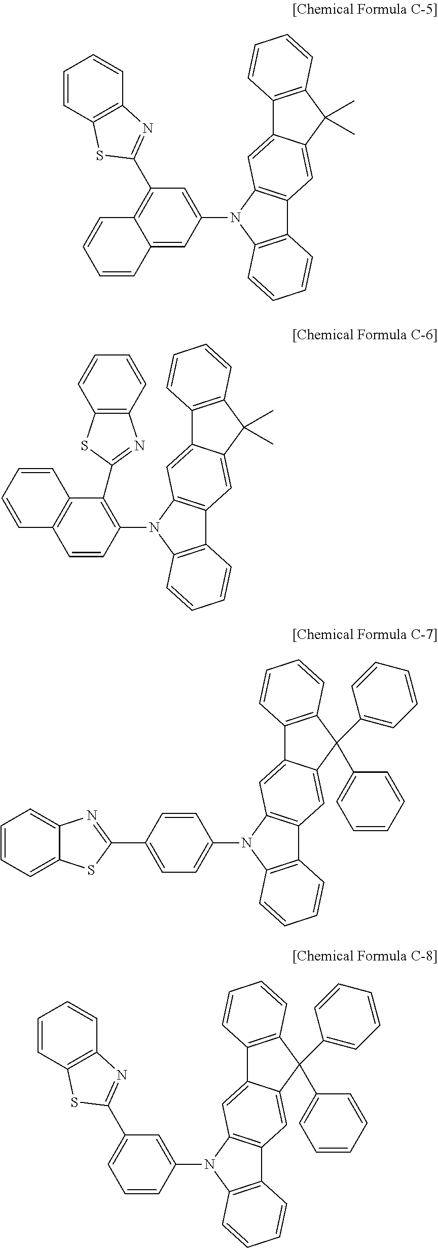


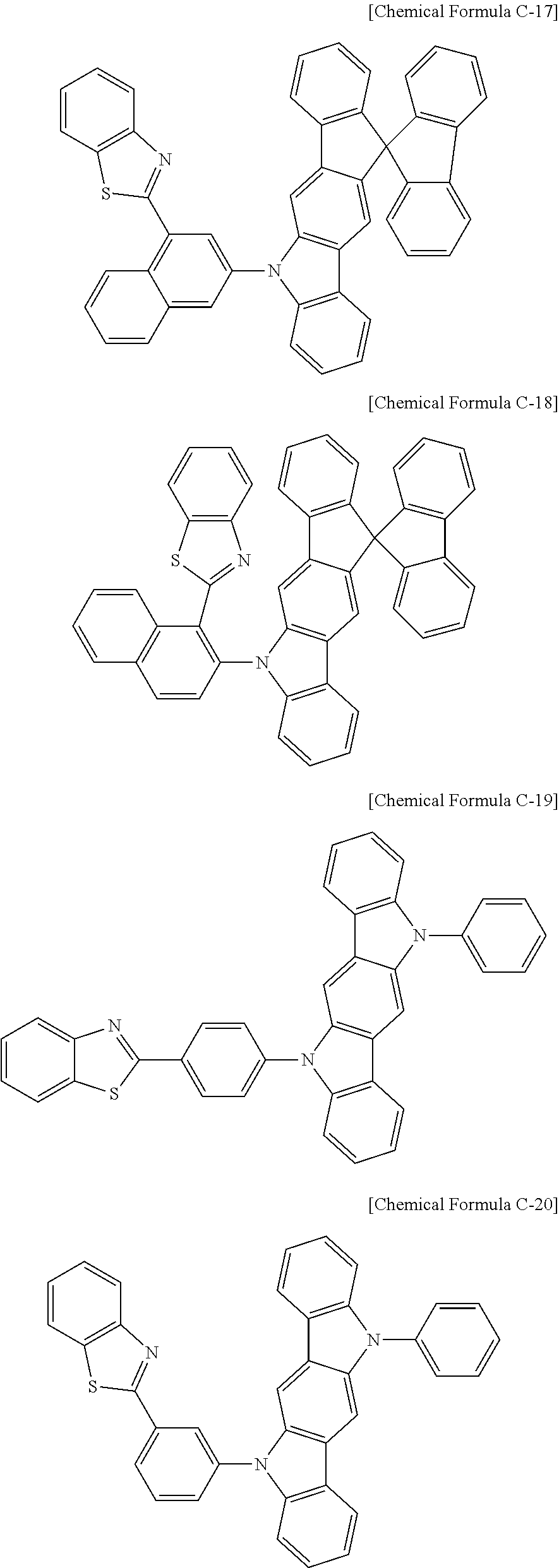


The compound for an organic optoelectronic device according to one embodiment of the present invention may be one of compounds represented by the following Chemical Formulae D-1 to D-8.


When the above compound according to one embodiment of the present invention requires both electron and hole characteristics, the functional group having electron characteristics may be introduced to effectively improve life-span of an organic light emitting diode and decreasing its driving voltage.
The above compound for an organic optoelectronic device according to one embodiment of the present invention shows a maximum light emitting wavelength in a range of about 320 to about 500 nm, high triplet exciton energy (T1) of greater than equal to about 2.0 eV and specifically, about 2.0 to about 4.0 eV and thus, has an advantage of increasing luminous efficiency of a to dopant by well transporting charges of a host having high triplet exciton energy to the dopant and decreasing a driving voltage by freely adjusting HOMO and LUMO energy levels of a material and accordingly, may be used as a host material or a charge transport material.
In addition, the compound for an organic optoelectronic device has optical and electrical activity and thus, may be used as a non-linear optical material, an electrode material, an electrochromic material, an optical switch, a sensor, a module, a wave guide, an organic transistor, a laser, an optical absorbing material, a dielectric material, and a material for a separation membrane and the like.
The compound for an organic optoelectronic device including the above compounds has a glass transition temperature of greater than or equal to about 90° C. and a thermal decomposition temperature of greater than or equal to about 400° C., indicating improved thermal stability. Thereby, it is possible to produce an organic optoelectronic device having a high efficiency.
The compound for an organic optoelectronic device including the above compounds may play a role for emitting light or injecting and/or transporting electrons, and also act as a light emitting host with an appropriate dopant. In other words, the compound for an organic optoelectronic device may be used as a phosphorescent or fluorescent host material, a blue light emitting dopant material, or an electron transport material.
The compound for an organic optoelectronic device according to one embodiment of the present invention is used for an organic thin layer, and it may improve the life-span characteristics, efficiency characteristics, electrochemical stability, and thermal stability of an organic optoelectronic device and decrease the driving voltage.
Therefore, according to another embodiment, an organic optoelectronic device that includes the compound for an organic optoelectronic device is provided. The organic optoelectronic device may include an organic photoelectric device, an organic light emitting diode, an organic solar cell, an organic transistor, an organic photo-conductor drum, an organic memory device, and the like. For example, the compound for an organic optoelectronic device according to one embodiment may be included in an electrode or an electrode buffer layer in the organic solar cell to improve the quantum efficiency, and it may be used as an electrode material for a gate, a source-drain electrode, or the like in the organic transistor.
Hereinafter, an organic light emitting diode is specifically described.
An organic light emitting diode according to another embodiment of the present invention includes an anode, a cathode, and at least one or more organic thin layer between the anode and the cathode, and at least one of the organic thin layers may include the compound for an organic optoelectronic device according to one embodiment of the present invention.
The organic thin layer including the compound for an organic optoelectronic device may include a layer selected from an emission layer, a hole transport layer, a hole injection layer, an electron transport layer, an electron injection layer, a hole blocking layer, and a combination thereof. The at least one layer includes the compound for an organic optoelectronic device according to one embodiment. Particularly, the compound for an organic optoelectronic device according to one embodiment may be included in an electron transport layer or electron injection layer. In addition, when the compound for an organic optoelectronic device is included in the emission layer, the compound for an organic optoelectronic device may be included as a phosphorescent or fluorescent host, and particularly, as a fluorescent blue dopant material.
Referring to FIGS. 1 to 5 , organic light emitting diodes 100, 200, 300, 400, and 500 according to one embodiment include at least one organic thin layer 105 interposed between an anode 120 and a cathode 110.
The anode 120 includes an anode material having a large work function to help hole injection into an organic thin layer. Specific examples of the anode material include: a metal such as nickel, platinum, vanadium, chromium, copper, zinc, and gold, or alloys thereof; a metal oxide such as zinc oxide, indium oxide, indium tin oxide (ITO), and indium zinc oxide (IZO); a combined metal and oxide such as ZnO:Al or SnO2:Sb; or a conductive polymer such as poly(3-methylthiophene), poly[3,4-(ethylene-1,2-dioxy)thiophene] (PEDT), polypyrrole, and polyaniline, but is not limited thereto. It is preferable to include a transparent electrode including indium tin oxide (ITO) as an anode.
The cathode 110 includes a cathode material having a small work function to help electron injection into an organic thin layer. Specific examples of the cathode material include: a metal such as magnesium, calcium, sodium, potassium, titanium, indium, yttrium, lithium, gadolinium, aluminum, silver, tin, and lead, or alloys thereof; or a multi-layered material such as LiF/Al, Liq/Al, LiO2/Al, LiF/Ca, LiF/Al, and BaF2/Ca, but is not limited thereto. It is preferable to include a metal electrode including aluminum as a cathode.
First, referring to FIG. 1 , the organic light emitting diode 100 includes an organic thin layer 105 including only an emission layer 130.
Referring to FIG. 2 , a double-layered organic light emitting diode 200 includes an organic thin layer 105 including an emission layer 230 including an electron transport layer (ETL), and a hole transport layer (HTL) 140. As shown in FIG. 2 , the organic thin layer 105 includes a double layer of the emission layer 230 and hole transport layer (HTL) 140. The emission layer 130 also functions as an electron transport layer (ETL), and the hole transport layer (HTL) 140 layer has an excellent binding property with a transparent electrode such as ITO or an excellent hole transport capability.
Referring to FIG. 3 , a three-layered organic light emitting diode 300 includes an organic thin layer 105 including an electron transport layer (ETL) 150, an emission layer 130, and a hole transport layer (HTL) 140. The emission layer 130 is independently installed, and layers having an excellent electron transport capability or an excellent hole transport capability are separately stacked.
As shown in FIG. 4 , a four-layered organic light emitting diode 400 includes an organic thin layer 105 including an electron injection layer (EIL) 160, an emission layer 130, a hole transport layer (HTL) 140, and a hole injection layer (HIL) 170 for adherence with the cathode of ITO.
As shown in FIG. 5 , a five-layered organic light emitting diode 500 includes an organic thin layer 105 including an electron transport layer (ETL) 150, an emission layer 130, a hole transport layer (HTL) 140, and a hole injection layer (HIL) 170, and further includes an electron injection layer (EIL) 160 to achieve a low voltage.
In FIGS. 1 to 5 , the organic thin layer 105 including at least one selected from the group consisting of an electron transport layer (ETL) 150, an electron injection layer (EIL) 160, emission layers 130 and 230, a hole transport layer (HTL) 140, a hole injection layer (HIL) 170, and combinations thereof includes the compound for an organic optoelectronic device. The compound for an organic optoelectronic device may be used for an electron transport layer (ETL) 150 including the electron transport layer (ETL) 150 or electron injection layer (EIL) 160. When it is used for the electron transport layer (ETL), it is possible to provide an organic light emitting diode having a more simple structure because it does not require an additional hole blocking layer (not shown).
Furthermore, when the compound for an organic optoelectronic device is included in the emission layers 130 and 230, the compound for an organic optoelectronic device may be included as a phosphorescent or fluorescent host or a fluorescent blue dopant.
The organic light emitting diode may be manufactured by: forming an anode on a substrate; forming an organic thin layer in accordance with a dry coating method such as evaporation, sputtering, plasma plating, and ion plating or a wet coating method such as spin coating, dipping, and flow coating; and providing a cathode thereon.
Another embodiment of the present invention provides a display device including the light emitting diode according to the above embodiment.
Hereinafter, the embodiments are illustrated in more detail with reference to examples. These examples, however, should not in any sense be interpreted as limiting the scope of the present invention.
A compound represented by the above formula A-1 as specific examples of a compound for an organic optoelectronic device according to the present invention was synthesized in a method of the following reaction scheme 1.

First Step: Synthesis of Compound (A)
37 g (0.3 mol) of 2-amino thiophenol, 50 g (0.27 mol) of 4-bromo benzaldehyde were agitated with 400 mL of dimethyl sulfoxide in a 1000 mL round flask, while the flask was heated up to a reflux temperature, and then, the mixture was agitated for 25 hours. The reaction solution was treated with water to produce a solid, the solid was dissolved in methylene chloride again, and then, moisture therein was removed by using anhydrous magnesium sulfate. After removing a solvent therein, 50 g of a compound (A) was obtained by holding a precipitate in methanol (a yield: 65%).
The obtained compound (A) was element-analyzed, and the result is provided as follows.
calcd. C13H8BrNS: C, 53.81; H, 2.78; N, 4.83; S, 11.05.
found: C, 53.51; H, 2.82; N, 4.75; S, 11.10.
Second Step: Synthesis of Compound A-1
13.8 g (50 mmol) of the compound (A), 17 g (40 mmol) of 9-phenyl-9H,9′H-[3,3′]bicarbazol-yl (B), and 7.6 g (55 mmol) of potassium carbonate were suspended in 250 ml of DMSO, 1 g (7 mmol) of 1,10-phenanthroline and 1 g (7 mmol) of copper chloride were added thereto, and the mixture was heated and refluxed under a nitrogen stream for 12 hours. The reaction solution was added to 1000 ml of MeOH, a solid crystallized therein was filtered and dissolved in monochlorobenzene and then, filtered with silica gel/Celite. After removing an organic solvent in an appropriate amount therefrom, a product was recrystallized in MeOH, obtaining 15 g of a compound A1 (a yield: 56%).
The obtained compound A-1 was element-analyzed, and the result is provided as follows.
calcd. C43H27N3S: C, 83.60; H, 4.41; N, 6.80; S, 5.19.
found: C, 83.35; H, 4.30; N, 6.78; S, 5.08.
A compound represented by the above formula A-4 as specific examples of a compound for an organic optoelectronic device according to the present invention was synthesized in a method according to the following reaction scheme 2.

First Step: Synthesis of Compound A-4
10.3 g (40 mmol) of the compound (A), 15 g (40 mmol) of 9-phenyl-9H,9′H-[3,3′]bicarbazol-yl (C), and 7.5 g (53 mmol) of potassium carbonate were suspended in 250 ml of DMSO, 1 g (7 mmol) of 1,10-phenanthroline and 1 g (7 mmol) of copper chloride were added thereto, and the mixture was heated and refluxed under a nitrogen stream for 12 hours. The reaction solution was added to 1000 ml of MeOH, a solid crystallized therein was filtered, dissolved in monochlorobenzene, and then, filtered through silica gel/Celite. After removing an organic solvent in an appropriate amount therefrom, a product was recrystallized in MeOH, obtaining 16.5 g of a compound A7 (a yield: 65%).
The obtained compound A-4 was element-analyzed, and the result is provided as follows.
calcd. C49H31N3S: C, 84.82; H, 4.50; N, 6.06; S, 4.62.
found: C, 84.79; H, 4.48; N, 6.01; S, 4.59.
A compound represented by the above formula A-43 as specific examples of a compound for an organic optoelectronic device according to the present invention was synthesized in a method of the following reaction scheme 3.

First Step: Synthesis of Compound A-43
12 g (23.8 mmol) of the compound (D), 6 g (24.8 mmol) of 2-bromo dibenzo furan, and 1.5 g (1 mmol) of tetrakis triphenyl phosphine were suspended in 250 ml of toluene/tetrahydrofuran, 250 ml of a 2M potassium carbonate aqueous solution was added thereto, and the mixture was heated and refluxed under a nitrogen stream for 24 hours. The reaction solution was added to 1000 ml of MeOH, a solid crystallized therein was filtered, dissolved in monochlorobenzene, and then, filtered through silica gel/Celite. After removing an organic solvent in an appropriate amount therefrom, a product therein was recrystallized in MeOH, obtaining 8 g of a compound A-43 (a yield: 62%).
The obtained compound A-43 was element-analyzed, and the result is provided as follows.
calcd. C37H22N2OS: C, 81.89; H, 4.09; N, 5.16; S, 5.91.
found: C, 81.89; H, 4.11; N, 5.15; S, 5.86.
A compound represented by the above formula A-72 as specific examples of a compound for an organic optoelectronic device according to the present invention was synthesized in a method of the following reaction scheme 4.

First Step: Synthesis of Compound A-72
12 g (23.8 mmol) of the compound (D), 9.4 g (23.8 mmol) of the compound (F), and 1.3 g (1 mmol) of tetrakis triphenyl phosphine were suspended in 250 ml of toluene/tetrahydrofuran, 250 ml of a 2M potassium carbonate aqueous solution was added thereto, and the mixture was heated and refluxed under a nitrogen stream for 24 hours. The reaction solution was added to 1000 ml of MeOH, and a solid crystallized therein was filtered, dissolved in monochlorobenzene, and then, filtered through silica gel/Celite. After removing an organic solvent in an appropriate amount therefrom, a product was recrystallized in MeOH, obtaining 10 g of a compound A-72 (a yield: 60%).
The obtained compound A-72 was element-analyzed, and the result is provided as follows.
calcd. C49H31N3S: C, 84.82; H, 4.50; N, 6.06; S, 4.62.
found: C, 84.80; H, 4.52; N, 6.15; S, 4.59.
A compound of the above formula B-1 as specific examples of compound for an organic optoelectronic device according to the present invention was synthesized in a method of the following reaction scheme 5.

First Step: Synthesis of Compound B-1
12 g (23.8 mmol) of the compound (D), 7.7 g (23.8 mmol) of a 4-bromo triphenyl amine compound, and 1.3 g (1 mmol) of tetrakis triphenyl phosphine were suspended in 250 ml of toluene/tetrahydrofuran, 250 ml of a 2M potassium carbonate aqueous solution was added thereto, and the mixture was heated and refluxed under a nitrogen stream for 24 hours. The reaction solution was added to 1000 ml of MeOH, and a solid crystallized therein was filtered, dissolved in monochlorobenzene, and then, filtered through silica gel/Celite. After removing an organic solvent in an appropriate amount therefrom, a product was recrystallized in MeOH, obtaining 8.8 g of a compound B-1 (a yield: 60%).
The obtained compound B-1 was element-analyzed, and the result is provided as follows.
calcd. C43H29N3S: C, 83.33; H, 4.72; N, 6.78; S, 5.17.
found: C, 83.37; H, 4.69; N, 6.71; S, 5.12.
A compound of the above formula D-1 was synthesized as specific examples of a compound for an organic optoelectronic device according to the present invention in a method of the following reaction scheme 6.

First Step: Synthesis of Compound D-1
12 g (23.8 mmol) of the compound (D), 7.3 g (23.8 mmol) of a 2-bromo triphenylene compound, and 1.3 g (1 mmol) of tetrakis triphenyl phosphine were suspended in 250 ml of toluene/tetrahydrofuran, 250 ml of a 2M potassium carbonate aqueous solution was added thereto, and the mixture was heated and refluxed under a nitrogen stream for 24 hours. The reaction solution was added to 1000 ml of MeOH, and a solid crystallized thereon was filtered, dissolved in monochlorobenzene, and then, filtered through silica gel/Celite. After removing an organic solvent in an appropriate amount therefrom, a product was recrystallized in MeOH, obtaining 8.5 g of a compound D-1 (a yield: 60%).
The obtained compound D-1 was element-analyzed, and the result is provided as follows.
calcd. C43H26N2S: C, 85.68; H, 4.35; N, 4.65; S, 5.32.
found: C, 85.67; H, 4.35; N, 4.65; S, 5.30.
A compound represented by the above formula R-1 as specific Comparative Examples of a compound for an organic optoelectronic device according to the present invention was synthesized in a method of the following reaction scheme 7.

First Step: Synthesis of Compound R-1
31.2 g (110 mmol) of the compound (A), 15 g (90 mmol) of N—H-carbazole (G), and 7.5 g (53 mmol) of potassium carbonate were suspended in 250 ml of DMSO, 1 g (7 mmol) of 1,10-phenanthroline and 1 g (7 mmol) of copper chloride were added thereto, and the mixture was heated and refluxed under a nitrogen stream for 24 hours. The reaction solution was added to 1000 ml of MeOH, and a solid crystallized therein was filtered, dissolved in monochlorobenzene, and then, filtered through silica gel/Celite. After removing an organic solvent in an appropriate amount therefrom, a product was recrystallized in MeOH, obtaining 20 g of a compound R-1 (a yield: 60%).
The obtained compound R-1 was element-analyzed, and the result is provided as follows.
calcd. C25H16N2S: C, 79.76; H, 4.28; N, 7.44; S, 8.52.
found: C, 79.69; H, 4.28; N, 7.39; S, 8.55.
A compound represented by the above formula R-2 as specific Comparative Examples of a compound for an organic optoelectronic device according to the present invention was synthesized in a method of the following reaction scheme 8.

First Step: Synthesis of Compound R-2
31.2 g (110 mmol) of the compound (A), 15 g (90 mmol) of N—H-carbazole (G), and 7.5 g (53 mmol) of potassium carbonate were suspended in 250 ml of DMSO, 1 g (7 mmol) of 1,10-phenanthroline and 1 g (7 mmol) of copper chloride were added thereto, and the mixture was heated and refluxed under a nitrogen stream for 24 hours. The reaction solution was added to 1000 ml of MeOH, and a solid crystallized therein was filtered, dissolved in monochlorobenzene, and then, filtered through silica gel/Celite. After removing an organic solvent in an appropriate amount therefrom, a product was recrystallized in MeOH, obtaining 23 g of a compound R-2 (a yield: 63%).
The obtained compound R-2 was element-analyzed, and the result is provided as follows.
calcd. C25H16N20: C, 83.31; H, 4.47; N, 7.77.
found: C, 83.33; H, 4.48; N, 7.73.
Specifically illustrating a method of manufacturing an organic light-emitting device, a anode is manufactured by cutting an ITO glass substrate having sheet resistance of 15 Ω/cm2 into a size of 50 mm×50 mm×0.7 mm, respectively washing the cut substrate with an ultrasonic wave in acetone, isopropylalcohol, and pure water for 15 minutes, and then, cleaning it with an UV ozone for 30 minutes.
Subsequently, the following HTM compound was vacuum-deposited to form a 1200 Å-thick hole injection layer on this ITO transparent electrode as a anode.

The compound synthesized according to Example 1 was used as a host and doped with 7 wt % of the following PhGD compound as a green phosphorescence dopant and then, vacuum-deposited to form a 300 Å-thick emission layer. Herein, a 1000 Å-thick ITO was used as for the anode, and a 1000 Å-thick aluminum (Al) was used as for a negative electrode.

Subsequently, BAlq [Bis(2-methyl-8-quinolinolato-N1,O8)-(1,1′-Biphenyl-4-olato)aluminum] was laminated to be 50 Å-thick, and Alq3 [Tris(8-hydroxyquinolinato)aluminium] was sequentially laminated to be 250 Å thick to form an electron transport layer on the emission layer. On the electron-transport layer, LiF and Al were sequentially vacuum-deposition to respectively be 5 Å thick and 1000 Å thick to form a cathode, manufacturing an organic light-emitting device.

An organic light-emitting device was manufactured according to the same method as Example 7 except for using the compound according to Example 2 instead of the compound according to Example 1 in Example 7.
An organic light-emitting device was manufactured according to the same method as Example 7 except for using the compound according to Example 4 instead of the compound according to Example 1 in Example 7.
Specifically, an organic light-emitting device was manufactured by cutting an ITO glass substrate having sheet resistance of 15 Ω/cm2 into a size of 50 mm×50 mm×0.7 mm, washing the cut substrate with an ultrasonic wave in acetone, isopropylalcohol, and pure water for 15 minutes respectively and then, cleaning it with an UV ozone for 30 minutes.
This ITO transparent electrode was used as a anode, and a hole injection layer was formed to be 1200 Å thick thereon by vacuum-depositing the following HTM compound and the compound according to Example 1 on the ITO substrate.

On the hole injection layer, a 300 Å-thick emission layer was formed by using 4,4-N,N-dicarbazolebiphenyl (CBP) as a host and doping it with 7 wt % of the following PhGD compound as a green phosphorescence dopant. Herein, a 1000 Å-thick ITO was used as for an anode, and a 1000 Å-thick aluminum (Al) was used as for a negative electrode.

Subsequently, 50 Å-thick BAlq [bis(2-methyl-8-quinolinolato-N1,O8)-(1,1′-biphenyl-4-olato)aluminum] and 250 Å-thick Alq3 [tris(8-hydroxyquinolinato)aluminium] were sequentially laminated to form an electron-transport layer on the emission layer. On the electron transport layer, 5 Å-thick LiF and 1000 Å-thick Al were sequentially vacuum-deposited to form a cathode, manufacturing an organic light-emitting device.

An organic light-emitting device was manufactured according to the same method as Example 10 except for using the compound of Example 2 instead of the compound of Example 1 in Example 10.
An organic light-emitting device was manufactured according to the same method as Example 10 except for using the compound of Example 4 instead of the compound of Example 1 in Example 10.
An organic light-emitting device was manufactured according to the same method as Example 7 except for using 4,4-N,N-dicarbazolebiphenyl (CBP) instead of the compound synthesized according to Example 1 as a host for an emission layer in Example 1.
An organic light-emitting device was manufactured according to the same method as Example 7 except for using the compound R1 synthesized according to Comparative Example 1 as a host for an emission layer instead of 4,4-N,N-dicarbazolebiphenyl (CBP) in Comparative Example 3.
An organic light-emitting device was manufactured according to the same method as Example 7 except for using the compound R2 synthesized according to Comparative Example 2 as a host for an emission layer instead of 4,4-N,N-dicarbazolebiphenyl (CBP) in Comparative Example 3.
Current density change, luminance change, and luminous efficiency of each organic light emitting diode according to Examples 8 to 12 and Comparative Examples 3 to 5 depending on a voltage were measured. Specific measurement methods are as follows, and the results are shown in the following Tables 1 and 2.
(1) Measurement of Current Density Change Depending on Voltage Change
The obtained organic light emitting diodes were measured for current value flowing in the unit device while increasing the voltage from 0 V to 10 V using a current-voltage meter (Keithley 2400), and the measured current value was divided by area to provide the result.
(2) Measurement of Luminance Change Depending on Voltage Change
Luminance was measured by using a luminance meter (Minolta Cs-1000A), while the voltage of the organic light emitting diodes was increased from 0 V to 10 V.
(3) Measurement of Luminous Efficiency
The luminance, current density, and voltage obtained from the (1) and (2) were used to calculate current efficiency (cd/A) and power efficiency (lm/W).
| TABLE 1 | ||||||
| Driving | Current | Power | Color | Color | ||
| voltage | efficiency | efficiency | Luminance | coordinate | coordinate | |
| (Vd, V) | (cd/A) | (lm/W) | (cd/m2) | (CIEx) | (CIEy) | |
| Comparative | 3.37 | 37.2 | 36 | 3000 | 0.341 | 0.625 |
| Example 3 | ||||||
| Comparative | 3.30 | 40.2 | 39.1 | 3000 | 0.350 | 0.620 |
| Example 4 | ||||||
| Comparative | 3.28 | 38.2 | 34.4 | 3000 | 0.341 | 0.645 |
| Example 5 | ||||||
| Example 8 | 3.28 | 41.8 | 40.5 | 3000 | 0.350 | 0.620 |
| Example 9 | 3.46 | 48.9 | 46.1 | 3000 | 0.350 | 0.619 |
The devices according to Examples 8 and 9 showed excellent characteristics compared with the devices according to Comparative Examples 3 to 5.
In addition, current density change, luminance change, and emission efficiency of the organic light-emitting devices respectively including an interlayer according to Examples 10 to 12 depending on voltage change were measured, and the results are provided in the following Table 2.
| TABLE 2 | ||||||
| Driving | Current | Power | Color | Color | ||
| voltage | efficiency | efficiency | Luminance | coordinate | coordinate | |
| (Vd, V) | (cd/A) | (lm/W) | (cd/m2) | (CIEx) | (CIEy) | |
| Comparative | 3.37 | 37.2 | 36 | 3000 | 0.341 | 0.625 |
| Example 3 | ||||||
| Example 10 | 4.31 | 51.1 | 37.2 | 3000 | 0.323 | 0.674 |
| Example 11 | 4.14 | 52.5 | 39.8 | 3000 | 0.322 | 0.654 |
| Example 12 | 4.13 | 49.8 | 37.8 | 3000 | 0.319 | 0.649 |
The devices including an interlayer according to Examples 10 to 12 showed improved efficiency compared with a device manufactured by applying CBP as a single host for an emission layer according to Comparative Example 3.
While this invention has been described in connection with what is presently considered to be practical exemplary embodiments, it is to be understood that the invention is not limited to the disclosed embodiments, but, on the contrary, is intended to cover various modifications and equivalent arrangements included within the spirit and scope of the appended claims. Therefore, the aforementioned embodiments should be understood to be exemplary but not limiting the present invention in any way.
Claims (19)
1. A compound for an organic optoelectronic device represented by the following Chemical Formula 1:

wherein, in the above Chemical Formula 1,
L1 is a substituted or unsubstituted C6 to C30 arylene group or a substituted or unsubstituted C2 to C30 heteroarylene group,
R1 and R2 are independently hydrogen, deuterium, a substituted or unsubstituted C1 to C10 alkyl group, a substituted or unsubstituted C6 to C30 aryl group, a substituted or unsubstituted C2 to C30 heteroaryl group, or a combination thereof,
R3 to R6 are independently hydrogen, deuterium, a substituted or unsubstituted amine group, a substituted or unsubstituted C1 to C10 alkyl group, a substituted or unsubstituted C6 to C30 aryl group, a substituted or unsubstituted C2 to C30 heteroaryl group, or a combination thereof,
at least one of R3 to R6 is a substituted or unsubstituted carbazolyl group, a substituted or unsubstituted dibenzofuranyl group, a substituted or unsubstituted dibenzothiophenyl group, a substituted or unsubstituted fluorenyl group, a substituted or unsubstituted amine group, or a substituted or unsubstituted triphenylenyl group or R3 and R4 are fused to each other to provide a ring, and
when R3 and R4 are fused to each other to provide a ring, the compound represented by Chemical Formula 1 is represented by the following Chemical Formula 3,

wherein, in the above Chemical Formula 3,
L1 is a substituted or unsubstituted C6 to C30 arylene group or a substituted or unsubstituted C2 to C30 heteroarylene group,
R1 to R6 are each independently hydrogen, deuterium, a substituted or unsubstituted C1 to C10 alkyl group, a substituted or unsubstituted C6 to C30 aryl group, a substituted or unsubstituted C2 to C30 heteroaryl group, or a combination thereof,
X is —NR7—, wherein R7 is hydrogen, deuterium, a substituted or unsubstituted C1 to C10 alkyl group, a substituted or unsubstituted C6 to C30 aryl group, a substituted or unsubstituted C2 to C30 heteroaryl group, or a combination thereof.
2. The compound for an organic optoelectronic device of claim 1 , wherein the compound for an organic optoelectronic device represented by the above Chemical Formula 1 is represented by the following Chemical Formula 2:

wherein, in the above Chemical Formula 2,
L1 and L2 are independently a substituted or unsubstituted C6 to C30 arylene group or a substituted or unsubstituted C2 to C30 heteroarylene group,
n is an integer ranging from 0 to 3,
R1 to R8 are independently hydrogen, deuterium, a substituted or unsubstituted C1 to C10 alkyl group, a substituted or unsubstituted C6 to C30 aryl group, a substituted or unsubstituted C2 to C30 heteroaryl group, or a combination thereof,
X is —NR9—, —O—, —S— or —CR10R11—, wherein the R9 to R11 are independently hydrogen, deuterium, a substituted or unsubstituted C1 to C10 alkyl group, a substituted or unsubstituted C6 to C30 aryl group, a substituted or unsubstituted C2 to C30 heteroaryl group, or a combination thereof, or
the R10 and R11 are fused to each other to provide a ring.
3. The compound for an organic optoelectronic device of claim 1 , wherein the compound for an organic optoelectronic device represented by the above Chemical Formula 1 is represented by the following Chemical Formula 4:

wherein, in the above Chemical Formula 4,
L1 and L2 are independently a substituted or unsubstituted C6 to C30 arylene group or a substituted or unsubstituted C2 to C30 heteroarylene group,
R1 to R5 are independently hydrogen, deuterium, a substituted or unsubstituted C1 to C10 alkyl group, a substituted or unsubstituted C6 to C30 aryl group, a substituted or unsubstituted C2 to C30 heteroaryl group, or a combination thereof, and
Ar1 and Ar2 are independently a substituted or unsubstituted C1 to C10 alkyl group, a substituted or unsubstituted C6 to C30 aryl group, a substituted or unsubstituted C2 to C30 heteroaryl group, or a combination thereof.
4. The compound for an organic optoelectronic device of claim 1 , wherein the compound for an organic optoelectronic device represented by the above Chemical Formula 1 is represented by the following Chemical Formula 5:

wherein, in the above Chemical Formula 5,
R1 and R2 are independently hydrogen, deuterium, a substituted or unsubstituted C1 to C10 alkyl group, a substituted or unsubstituted C6 to C30 aryl group, a substituted or unsubstituted C2 to C30 heteroaryl group, or a combination thereof,
R3 to R6 are independently hydrogen, deuterium, a substituted or unsubstituted amine group, a substituted or unsubstituted C1 to C10 alkyl group, a substituted or unsubstituted C6 to C30 aryl group, a substituted or unsubstituted C2 to C30 heteroaryl group, or a combination thereof,
at least one of R3 to R6 is a substituted or unsubstituted carbazolyl group, a substituted or unsubstituted dibenzofuranyl group, a substituted or unsubstituted dibenzothiophenyl group, a substituted or unsubstituted fluorenyl group, a substituted or unsubstituted amine group, or a substituted or unsubstituted triphenylenyl group or R3 and R4 are fused to each other to provide a ring, and
when R3 and R4 are fused to each other to provide a ring, the compound represented by Chemical Formula 1 is represented by the following Chemical Formula 3,

wherein, in the above Chemical Formula 3,
L1 is a substituted or unsubstituted C6 to C30 arylene group or a substituted or unsubstituted C2 to C30 heteroarylene group,
R1 to R6 are each independently hydrogen, deuterium, a substituted or unsubstituted C1 to C10 alkyl group, a substituted or unsubstituted C6 to C30 aryl group, a substituted or unsubstituted C2 to C30 heteroaryl group, or a combination thereof,
X is —NR7—, wherein R7 is hydrogen, deuterium, a substituted or unsubstituted C1 to C10 alkyl group, a substituted or unsubstituted C6 to C30 aryl group, a substituted or unsubstituted C2 to C30 heteroaryl group, or a combination thereof.
5. The compound for an organic optoelectronic device of claim 1 , wherein the compound for an organic optoelectronic device represented by the above Chemical Formula 1 is represented by the following Chemical Formula 6:

wherein, in the above Chemical Formula 6,
R1 and R2 are independently hydrogen, deuterium, a substituted or unsubstituted C1 to C10 alkyl group, a substituted or unsubstituted C6 to C30 aryl group, a substituted or unsubstituted C2 to C30 heteroaryl group, or a combination thereof,
R3 to R6 are independently hydrogen, deuterium, a substituted or unsubstituted amine group, a substituted or unsubstituted C1 to C10 alkyl group, a substituted or unsubstituted C6 to C30 aryl group, a substituted or unsubstituted C2 to C30 heteroaryl group, or a combination thereof,
at least one of R3 to R6 is a substituted or unsubstituted carbazolyl group, a substituted or unsubstituted dibenzofuranyl group, a substituted or unsubstituted dibenzothiophenyl group, a substituted or unsubstituted fluorenyl group, a substituted or unsubstituted amine group, or a substituted or unsubstituted triphenylenyl group or R3 and R4 are fused to each other to provide a ring, and
when R3 and R4 are fused to each other to provide a ring, the compound represented by Chemical Formula 1 is represented by the following Chemical Formula 3,

wherein, in the above Chemical Formula 3,
L1 is a substituted or unsubstituted C6 to C30 arylene group or a substituted or unsubstituted C2 to C30 heteroarylene group,
R1 to R6 are each independently hydrogen, deuterium, a substituted or unsubstituted C1 to C10 alkyl group, a substituted or unsubstituted C6 to C30 aryl group, a substituted or unsubstituted C2 to C30 heteroaryl group, or a combination thereof,
X is —NR7—, wherein R7 is hydrogen, deuterium, a substituted or unsubstituted C1 to C10 alkyl group, a substituted or unsubstituted C6 to C30 aryl group, a substituted or unsubstituted C2 to C30 heteroaryl group, or a combination thereof.
6. The compound for an organic optoelectronic device of claim 1 , wherein the compound for an organic optoelectronic device represented by the above Chemical Formula 1 is represented by the following Chemical Formula 7:

wherein, in the above Chemical Formula 7,
R1 and R2 are independently hydrogen, deuterium, a substituted or unsubstituted C1 to C10 alkyl group, a substituted or unsubstituted C6 to C30 aryl group, a substituted or unsubstituted C2 to C30 heteroaryl group, or a combination thereof,
R3 to R6 are independently hydrogen, deuterium, a substituted or unsubstituted amine group, a substituted or unsubstituted C1 to C10 alkyl group, a substituted or unsubstituted C6 to C30 aryl group, a substituted or unsubstituted C2 to C30 heteroaryl group, or a combination thereof,
at least one of R3 to R6 is a substituted or unsubstituted carbazolyl group, a substituted or unsubstituted dibenzofuranyl group, a substituted or unsubstituted dibenzothiophenyl group, a substituted or unsubstituted fluorenyl group, a substituted or unsubstituted amine group, or a substituted or unsubstituted triphenylenyl group or R3 and R4 are fused to each other to provide a ring, and
when R3 and R4 are fused to each other to provide a ring, the compound represented by Chemical Formula 1 is represented by the following Chemical Formula 3,

wherein, in the above Chemical Formula 3,
L1 is a substituted or unsubstituted C6 to C30 arylene group or a substituted or unsubstituted C2 to C30 heteroarylene group,
R1 to R6 are each independently hydrogen, deuterium, a substituted or unsubstituted C1 to C10 alkyl group, a substituted or unsubstituted C6 to C30 aryl group, a substituted or unsubstituted C2 to C30 heteroaryl group, or a combination thereof,
X is —NR7—, wherein R7 is hydrogen, deuterium, a substituted or unsubstituted C1 to C10 alkyl group, a substituted or unsubstituted C6 to C30 aryl group, a substituted or unsubstituted C2 to C30 heteroaryl group, or a combination thereof.
7. The compound for an organic optoelectronic device of claim 1 , wherein the L1 is a substituted or unsubstituted phenylene group or a substituted or unsubstituted naphthylene group.
8. The compound for an organic optoelectronic device of claim 1 , wherein the compound for an organic optoelectronic device is one of compounds represented by the following Chemical Formulae A-1 to A-74:


9. A compound for an organic optoelectronic device, wherein the compound for an organic optoelectronic device is one of compounds represented by the following Chemical Formulae B-1 to B-8:


10. The compound for an organic optoelectronic device of claim 1 , wherein the compound for an organic optoelectronic device is one of compounds represented by the following Chemical Formulae C-19 to C-45:


11. The compound for an organic optoelectronic device of claim 1 , wherein the compound for an organic optoelectronic device is one of compounds represented by the following Chemical Formulae D-1 to D-8:


12. The compound for an organic optoelectronic device of claim 1 , wherein the compound for an organic optoelectronic device has triplet exciton energy (T1) of greater than or equal to about 2.0 eV.
13. The compound for an organic optoelectronic device of claim 1 , wherein the organic optoelectronic device is selected from an organic photoelectric device, an organic light emitting diode, an organic solar cell, an organic transistor, an organic photo-conductor drum, and an organic memory device.
14. An organic light emitting diode, comprising
an anode, a cathode, and at least one organic thin layer interposed between the anode and cathode,
wherein at least one of the organic thin layers comprises the above compound for an organic optoelectronic device of claim 1 .
15. The organic light emitting diode of claim 14 , wherein the organic thin layer is selected from an emission layer, a hole transport layer, a hole injection layer, an electron transport layer, an electron injection layer, a hole blocking layer, and a combination thereof.
16. The organic light emitting diode of claim 15 , wherein the compound for an organic optoelectronic device is included in a hole transport layer (HTL) or a hole injection layer (HIL).
17. The organic light emitting diode of claim 15 , wherein the compound for an organic optoelectronic device is included in an emission layer.
18. The organic light emitting diode of claim 17 , wherein the compound for an organic optoelectronic device is used as a phosphorescent or fluorescent host material in an emission layer.
19. A display device comprising the above organic light emitting diode of claim 14 .
Applications Claiming Priority (4)
| Application Number | Priority Date | Filing Date | Title |
|---|---|---|---|
| KR10-2011-0146193 | 2011-12-29 | ||
| KR1020110146193A KR101507004B1 (en) | 2011-12-29 | 2011-12-29 | Compound for organic optoelectronic device, organic light emitting diode including the same and display including the organic light emitting diode |
| KR10-2011-146193 | 2011-12-29 | ||
| PCT/KR2012/011023 WO2013100465A1 (en) | 2011-12-29 | 2012-12-17 | Compound for organic optoelectronic element, organic light-emitting element comprising same, and display device comprising the organic light-emitting element |
Publications (2)
| Publication Number | Publication Date |
|---|---|
| US20140326984A1 US20140326984A1 (en) | 2014-11-06 |
| US9793488B2 true US9793488B2 (en) | 2017-10-17 |
Family
ID=48697846
Family Applications (1)
| Application Number | Title | Priority Date | Filing Date |
|---|---|---|---|
| US14/359,786 Active 2034-12-03 US9793488B2 (en) | 2011-12-29 | 2012-12-17 | Compound for organic optoelectronic element, organic light-emitting element comprising same, and display device comprising the organic light-emitting element |
Country Status (3)
| Country | Link |
|---|---|
| US (1) | US9793488B2 (en) |
| KR (1) | KR101507004B1 (en) |
| WO (1) | WO2013100465A1 (en) |
Families Citing this family (12)
| Publication number | Priority date | Publication date | Assignee | Title |
|---|---|---|---|---|
| CN103756670B (en) | 2014-01-23 | 2015-12-09 | 上海和辉光电有限公司 | Electroluminescent organic material and its preparation method and application |
| KR102151753B1 (en) * | 2014-02-13 | 2020-09-04 | 삼성디스플레이 주식회사 | Condensed compound and organic light emitting diode comprising the same |
| WO2015178115A1 (en) * | 2014-05-23 | 2015-11-26 | ソニー株式会社 | Photoelectric conversion element, solid-state imaging device, and organic light-absorbing material |
| KR101636137B1 (en) * | 2014-07-31 | 2016-07-04 | 포항공과대학교 산학협력단 | Organic doping material for memory device, nonvolatile memory device including the same and method of manufacturing the same |
| CN107001380B (en) * | 2015-01-13 | 2021-01-29 | 广州华睿光电材料有限公司 | Compound, mixture containing the same, composition and organic electronic device |
| CN106543157B (en) * | 2016-10-25 | 2019-09-20 | 上海道亦化工科技有限公司 | A kind of electroluminescent organic material and its organic electroluminescence device |
| KR102236322B1 (en) * | 2018-08-09 | 2021-04-05 | 주식회사 엘지화학 | Novel compound and organic light emitting device comprising the same |
| CN112300171B (en) * | 2019-07-30 | 2023-08-15 | 江苏三月科技股份有限公司 | Organic compound based on carbazolo ring structure and application of organic compound to OLED |
| CN114105997B (en) * | 2021-01-28 | 2023-05-19 | 陕西莱特光电材料股份有限公司 | Nitrogen-containing compound, and electronic element and electronic device comprising same |
| CN113764604B (en) * | 2021-04-13 | 2022-06-03 | 陕西莱特光电材料股份有限公司 | Composition, electronic component comprising same and electronic device |
| CN113421980B (en) * | 2021-06-02 | 2023-02-24 | 陕西莱特迈思光电材料有限公司 | Organic electroluminescent device and electronic apparatus including the same |
| WO2023013615A1 (en) * | 2021-08-02 | 2023-02-09 | 東ソー株式会社 | Amine compound, hole injection layer and organic electroluminescent element |
Citations (15)
| Publication number | Priority date | Publication date | Assignee | Title |
|---|---|---|---|---|
| JP2004067658A (en) | 2002-06-10 | 2004-03-04 | Mitsubishi Chemicals Corp | Organometallic complex and organic electroluminescent device by using the same |
| KR20060045360A (en) | 2004-04-01 | 2006-05-17 | 제너럴 일렉트릭 캄파니 | Electroactive polymer, device made therefrom and method |
| US20060125380A1 (en) * | 2004-12-13 | 2006-06-15 | Yoshiaki Nagara | Organic EL devices |
| US20080124572A1 (en) * | 2006-11-24 | 2008-05-29 | Idemitsu Kosan Co., Ltd. | Aromatic amine derivative and organic electroluminescence device using the same |
| KR20090119739A (en) | 2008-05-16 | 2009-11-19 | 가부시키가이샤 한도오따이 에네루기 켄큐쇼 | Benzoxazole derivative, and light-emitting element, light-emitting device, and electronic device using the same |
| KR20100002153A (en) | 2008-06-25 | 2010-01-06 | 다우어드밴스드디스플레이머티리얼 유한회사 | Novel organic electroluminescent compounds and organic electroluminescent device using the same |
| KR20100029040A (en) | 2008-09-05 | 2010-03-15 | 가부시키가이샤 한도오따이 에네루기 켄큐쇼 | Benzoxazole derivative, and light-emitting element, light-emitting device, and electronic device using benzoxazole derivative |
| WO2010041872A2 (en) | 2008-10-08 | 2010-04-15 | 주식회사 엘지화학 | Novel compound and organic electronic device using same |
| US20100200054A1 (en) * | 2007-10-17 | 2010-08-12 | Ho-Kuk Jung | Compound for organic photoelectric device and organic photoelectric device including the same |
| WO2010113726A1 (en) * | 2009-03-31 | 2010-10-07 | 新日鐵化学株式会社 | Material for use in phosphorescent device and organic electroluminescent device using same |
| WO2010136109A1 (en) * | 2009-05-29 | 2010-12-02 | Merck Patent Gmbh | Materials for organic electroluminescent devices |
| KR20110015836A (en) | 2009-08-10 | 2011-02-17 | 다우어드밴스드디스플레이머티리얼 유한회사 | Novel organic electroluminescent compounds and organic electroluminescent device using the same |
| KR20110043270A (en) * | 2009-10-21 | 2011-04-27 | (주)씨에스엘쏠라 | Organic light emitting compound and organic light emitting device comprising the same |
| WO2011132683A1 (en) | 2010-04-20 | 2011-10-27 | 出光興産株式会社 | Bis-carbazole derivative, material for organic electroluminescent element and organic electroluminescent element using same |
| US20120133274A1 (en) * | 2010-11-30 | 2012-05-31 | Semiconductor Energy Laboratory Co., Ltd. | Carbazole Compound, Light-Emitting Element Material, Organic Semiconductor Material, Light-Emitting Element, Light-Emitting Device, Lighting Device, and Electronic Device |
-
2011
- 2011-12-29 KR KR1020110146193A patent/KR101507004B1/en active IP Right Grant
-
2012
- 2012-12-17 WO PCT/KR2012/011023 patent/WO2013100465A1/en active Application Filing
- 2012-12-17 US US14/359,786 patent/US9793488B2/en active Active
Patent Citations (18)
| Publication number | Priority date | Publication date | Assignee | Title |
|---|---|---|---|---|
| JP2004067658A (en) | 2002-06-10 | 2004-03-04 | Mitsubishi Chemicals Corp | Organometallic complex and organic electroluminescent device by using the same |
| KR20060045360A (en) | 2004-04-01 | 2006-05-17 | 제너럴 일렉트릭 캄파니 | Electroactive polymer, device made therefrom and method |
| US20060125380A1 (en) * | 2004-12-13 | 2006-06-15 | Yoshiaki Nagara | Organic EL devices |
| US20080124572A1 (en) * | 2006-11-24 | 2008-05-29 | Idemitsu Kosan Co., Ltd. | Aromatic amine derivative and organic electroluminescence device using the same |
| US20100200054A1 (en) * | 2007-10-17 | 2010-08-12 | Ho-Kuk Jung | Compound for organic photoelectric device and organic photoelectric device including the same |
| KR20090119739A (en) | 2008-05-16 | 2009-11-19 | 가부시키가이샤 한도오따이 에네루기 켄큐쇼 | Benzoxazole derivative, and light-emitting element, light-emitting device, and electronic device using the same |
| KR20100002153A (en) | 2008-06-25 | 2010-01-06 | 다우어드밴스드디스플레이머티리얼 유한회사 | Novel organic electroluminescent compounds and organic electroluminescent device using the same |
| KR20100029040A (en) | 2008-09-05 | 2010-03-15 | 가부시키가이샤 한도오따이 에네루기 켄큐쇼 | Benzoxazole derivative, and light-emitting element, light-emitting device, and electronic device using benzoxazole derivative |
| WO2010041872A2 (en) | 2008-10-08 | 2010-04-15 | 주식회사 엘지화학 | Novel compound and organic electronic device using same |
| WO2010113726A1 (en) * | 2009-03-31 | 2010-10-07 | 新日鐵化学株式会社 | Material for use in phosphorescent device and organic electroluminescent device using same |
| US20110315975A1 (en) * | 2009-03-31 | 2011-12-29 | Takahiro Kai | Material for use in phosphorescent device and organic electroluminescent device using same |
| JPWO2010113726A1 (en) * | 2009-03-31 | 2012-10-11 | 新日鐵化学株式会社 | Phosphorescent light emitting device material and organic electroluminescent device using the same |
| WO2010136109A1 (en) * | 2009-05-29 | 2010-12-02 | Merck Patent Gmbh | Materials for organic electroluminescent devices |
| US20120068170A1 (en) * | 2009-05-29 | 2012-03-22 | Merck Patent Gmbh | Materials for organic electroluminescent devices |
| KR20110015836A (en) | 2009-08-10 | 2011-02-17 | 다우어드밴스드디스플레이머티리얼 유한회사 | Novel organic electroluminescent compounds and organic electroluminescent device using the same |
| KR20110043270A (en) * | 2009-10-21 | 2011-04-27 | (주)씨에스엘쏠라 | Organic light emitting compound and organic light emitting device comprising the same |
| WO2011132683A1 (en) | 2010-04-20 | 2011-10-27 | 出光興産株式会社 | Bis-carbazole derivative, material for organic electroluminescent element and organic electroluminescent element using same |
| US20120133274A1 (en) * | 2010-11-30 | 2012-05-31 | Semiconductor Energy Laboratory Co., Ltd. | Carbazole Compound, Light-Emitting Element Material, Organic Semiconductor Material, Light-Emitting Element, Light-Emitting Device, Lighting Device, and Electronic Device |
Non-Patent Citations (2)
| Title |
|---|
| Machine translation of JP2004-067658. Date of publication: Mar. 4, 2004. * |
| Machine translation of KR2011-0043270. Date of publication: Apr. 27, 2011. * |
Also Published As
| Publication number | Publication date |
|---|---|
| KR20130077469A (en) | 2013-07-09 |
| US20140326984A1 (en) | 2014-11-06 |
| WO2013100465A1 (en) | 2013-07-04 |
| KR101507004B1 (en) | 2015-03-30 |
Similar Documents
| Publication | Publication Date | Title |
|---|---|---|
| US10121973B2 (en) | Compound for organic optoelectronic device, organic light-emitting diode including same, and display device including organic light-emitting diode | |
| US10153436B2 (en) | Compound for an organic optoelectronic element, organic light-emitting element comprising same, and display device comprising the organic light-emitting element | |
| US9793488B2 (en) | Compound for organic optoelectronic element, organic light-emitting element comprising same, and display device comprising the organic light-emitting element | |
| US9324948B2 (en) | Compound for organic optoelectronic device, organic light emitting diode including the same and display including the organic light emitting diode | |
| US9543530B2 (en) | Compound for organic optoelectronic device, organic light emitting diode including the same and display including the organic light emitting diode | |
| US9406891B2 (en) | Compound for organic optoelectronic device, organic light emitting diode including the same, and display including the organic light emitting diode | |
| US9502662B2 (en) | Compound for an organic optoelectronic device, organic light-emitting element comprising same, and display device comprising the organic light-emitting element | |
| US20150263294A1 (en) | Compound for organic optoelectronic device, organic light-emitting device including same, and display device including the organic light- emitting diode | |
| US20150144937A1 (en) | Compound for organic optoelectronic device, organic light emitting diode comprising same, and display device comprising organic light emitting diode | |
| US9722186B2 (en) | Compound for organic optoelectronic device, organic light emitting diode comprising same, and display comprising organic light emitting diode | |
| US9899607B2 (en) | Compound for organic optoelectronic device, organic light emitting diode including the same and display including the organic light emitting diode | |
| US20130292659A1 (en) | Compound for organic optoelectronic device, organic light emitting diode including the same, and display device including the organic light emitting diode | |
| US20130200356A1 (en) | Compound for organic optoelectronic device, organic light emitting diode including the same and display including the organic light emitting diode | |
| US9299935B2 (en) | Nitrogen-containing heterocyclic compounds and organic electronic device comprising the same | |
| US9444054B2 (en) | Compound for organic optoelectronic device and organic light emitting diode including the same | |
| KR20140087996A (en) | Compound for organic optoelectronic device, organic light emitting diode including the same and display including the organic light emitting diode | |
| US20130256644A1 (en) | Compound for organic optoelectronic device, organic light emitting diode including the same and display including the organic light emitting diode | |
| US9540374B2 (en) | Nitrogen-containing heterocyclic compounds and organic electronic device comprising the same | |
| US20150021563A1 (en) | Compound for organic optoelectronic device, organic light emitting diode including the same and display including the organic light emitting diode | |
| US20180083202A1 (en) | Compound for organic optoelectric device, composition for organic optoelectric device and organic optoelectric device and display device | |
| US9825242B2 (en) | Compound for organic optoelectric device, organic light-emitting diode including same, display device including organic light-emitting diode | |
| US9543528B2 (en) | Compound for an organic optoelectric device, organic optoelectric device including the same, and display device including the optoelectric device | |
| US11056655B2 (en) | Organic compound for optoelectric device and organic optoelectric device and display device |
Legal Events
| Date | Code | Title | Description |
|---|---|---|---|
| AS | Assignment |
Owner name: CHEIL INDUSTRIES, INC., KOREA, REPUBLIC OF Free format text: ASSIGNMENT OF ASSIGNORS INTEREST;ASSIGNORS:PARK, MOO-JIN;YU, EUN-SUN;LEE, HO-JAE;AND OTHERS;REEL/FRAME:032981/0864 Effective date: 20140516 |
|
| STCF | Information on status: patent grant |
Free format text: PATENTED CASE |
|
| MAFP | Maintenance fee payment |
Free format text: PAYMENT OF MAINTENANCE FEE, 4TH YEAR, LARGE ENTITY (ORIGINAL EVENT CODE: M1551); ENTITY STATUS OF PATENT OWNER: LARGE ENTITY Year of fee payment: 4 |