US9722186B2 - Compound for organic optoelectronic device, organic light emitting diode comprising same, and display comprising organic light emitting diode - Google Patents
Compound for organic optoelectronic device, organic light emitting diode comprising same, and display comprising organic light emitting diode Download PDFInfo
- Publication number
- US9722186B2 US9722186B2 US14/669,511 US201514669511A US9722186B2 US 9722186 B2 US9722186 B2 US 9722186B2 US 201514669511 A US201514669511 A US 201514669511A US 9722186 B2 US9722186 B2 US 9722186B2
- Authority
- US
- United States
- Prior art keywords
- group
- substituted
- unsubstituted
- compound
- chemical formula
- Prior art date
- Legal status (The legal status is an assumption and is not a legal conclusion. Google has not performed a legal analysis and makes no representation as to the accuracy of the status listed.)
- Active, expires
Links
- 150000001875 compounds Chemical class 0.000 title claims abstract description 162
- 230000005693 optoelectronics Effects 0.000 title claims abstract description 67
- 239000000126 substance Substances 0.000 claims abstract description 82
- 125000001072 heteroaryl group Chemical group 0.000 claims description 30
- 125000003118 aryl group Chemical group 0.000 claims description 27
- 238000002347 injection Methods 0.000 claims description 24
- 239000007924 injection Substances 0.000 claims description 24
- 125000003808 silyl group Chemical group [H][Si]([H])([H])[*] 0.000 claims description 16
- -1 Y is N Inorganic materials 0.000 claims description 15
- 125000003277 amino group Chemical group 0.000 claims description 11
- 230000005525 hole transport Effects 0.000 claims description 11
- 125000004093 cyano group Chemical group *C#N 0.000 claims description 9
- 229910052736 halogen Inorganic materials 0.000 claims description 9
- 150000002367 halogens Chemical class 0.000 claims description 9
- 229910052739 hydrogen Inorganic materials 0.000 claims description 9
- 239000001257 hydrogen Substances 0.000 claims description 9
- 125000002887 hydroxy group Chemical group [H]O* 0.000 claims description 9
- 125000000449 nitro group Chemical group [O-][N+](*)=O 0.000 claims description 9
- 229910052760 oxygen Inorganic materials 0.000 claims description 9
- YZCKVEUIGOORGS-OUBTZVSYSA-N Deuterium Chemical group [2H] YZCKVEUIGOORGS-OUBTZVSYSA-N 0.000 claims description 8
- 125000004419 alkynylene group Chemical group 0.000 claims description 8
- 229910052799 carbon Inorganic materials 0.000 claims description 8
- 229910052805 deuterium Inorganic materials 0.000 claims description 8
- 229910052710 silicon Inorganic materials 0.000 claims description 8
- 125000004450 alkenylene group Chemical group 0.000 claims description 7
- 125000000732 arylene group Chemical group 0.000 claims description 7
- 125000003178 carboxy group Chemical group [H]OC(*)=O 0.000 claims description 7
- 125000005549 heteroarylene group Chemical group 0.000 claims description 7
- 150000002431 hydrogen Chemical group 0.000 claims description 7
- 125000004469 siloxy group Chemical group [SiH3]O* 0.000 claims description 7
- 125000000641 acridinyl group Chemical group C1(=CC=CC2=NC3=CC=CC=C3C=C12)* 0.000 claims description 4
- 125000003785 benzimidazolyl group Chemical group N1=C(NC2=C1C=CC=C2)* 0.000 claims description 4
- 125000000499 benzofuranyl group Chemical group O1C(=CC2=C1C=CC=C2)* 0.000 claims description 4
- 125000004196 benzothienyl group Chemical group S1C(=CC2=C1C=CC=C2)* 0.000 claims description 4
- 125000004622 benzoxazinyl group Chemical group O1NC(=CC2=C1C=CC=C2)* 0.000 claims description 4
- 125000002676 chrysenyl group Chemical group C1(=CC=CC=2C3=CC=C4C=CC=CC4=C3C=CC12)* 0.000 claims description 4
- 125000002541 furyl group Chemical group 0.000 claims description 4
- 125000002883 imidazolyl group Chemical group 0.000 claims description 4
- 125000003454 indenyl group Chemical group C1(C=CC2=CC=CC=C12)* 0.000 claims description 4
- 125000001041 indolyl group Chemical group 0.000 claims description 4
- 125000002183 isoquinolinyl group Chemical group C1(=NC=CC2=CC=CC=C12)* 0.000 claims description 4
- 125000004593 naphthyridinyl group Chemical group N1=C(C=CC2=CC=CN=C12)* 0.000 claims description 4
- 125000001715 oxadiazolyl group Chemical group 0.000 claims description 4
- 125000002971 oxazolyl group Chemical group 0.000 claims description 4
- 125000002080 perylenyl group Chemical group C1(=CC=C2C=CC=C3C4=CC=CC5=CC=CC(C1=C23)=C45)* 0.000 claims description 4
- 125000001791 phenazinyl group Chemical group C1(=CC=CC2=NC3=CC=CC=C3N=C12)* 0.000 claims description 4
- 125000001484 phenothiazinyl group Chemical group C1(=CC=CC=2SC3=CC=CC=C3NC12)* 0.000 claims description 4
- 125000001644 phenoxazinyl group Chemical group C1(=CC=CC=2OC3=CC=CC=C3NC12)* 0.000 claims description 4
- 125000003373 pyrazinyl group Chemical group 0.000 claims description 4
- 125000003226 pyrazolyl group Chemical group 0.000 claims description 4
- 125000004076 pyridyl group Chemical group 0.000 claims description 4
- 125000000714 pyrimidinyl group Chemical group 0.000 claims description 4
- 125000000168 pyrrolyl group Chemical group 0.000 claims description 4
- 125000002294 quinazolinyl group Chemical group N1=C(N=CC2=CC=CC=C12)* 0.000 claims description 4
- 125000002943 quinolinyl group Chemical group N1=C(C=CC2=CC=CC=C12)* 0.000 claims description 4
- 125000001567 quinoxalinyl group Chemical group N1=C(C=NC2=CC=CC=C12)* 0.000 claims description 4
- 125000001935 tetracenyl group Chemical group C1(=CC=CC2=CC3=CC4=CC=CC=C4C=C3C=C12)* 0.000 claims description 4
- 125000001113 thiadiazolyl group Chemical group 0.000 claims description 4
- 125000000335 thiazolyl group Chemical group 0.000 claims description 4
- 125000001544 thienyl group Chemical group 0.000 claims description 4
- 125000004306 triazinyl group Chemical group 0.000 claims description 4
- 125000001425 triazolyl group Chemical group 0.000 claims description 4
- 125000003960 triphenylenyl group Chemical group C1(=CC=CC=2C3=CC=CC=C3C3=CC=CC=C3C12)* 0.000 claims description 4
- YJTKZCDBKVTVBY-UHFFFAOYSA-N 1,3-Diphenylbenzene Chemical group C1=CC=CC=C1C1=CC=CC(C=2C=CC=CC=2)=C1 YJTKZCDBKVTVBY-UHFFFAOYSA-N 0.000 claims description 3
- 125000002178 anthracenyl group Chemical group C1(=CC=CC2=CC3=CC=CC=C3C=C12)* 0.000 claims description 3
- 230000000903 blocking effect Effects 0.000 claims description 3
- 125000001624 naphthyl group Chemical group 0.000 claims description 3
- 125000001997 phenyl group Chemical group [H]C1=C([H])C([H])=C(*)C([H])=C1[H] 0.000 claims description 3
- XJKSTNDFUHDPQJ-UHFFFAOYSA-N 1,4-diphenylbenzene Chemical group C1=CC=CC=C1C1=CC=C(C=2C=CC=CC=2)C=C1 XJKSTNDFUHDPQJ-UHFFFAOYSA-N 0.000 claims description 2
- 125000004653 anthracenylene group Chemical group 0.000 claims description 2
- 125000002529 biphenylenyl group Chemical group C1(=CC=CC=2C3=CC=CC=C3C12)* 0.000 claims description 2
- 125000005567 fluorenylene group Chemical group 0.000 claims description 2
- 125000004957 naphthylene group Chemical group 0.000 claims description 2
- 125000005561 phenanthryl group Chemical group 0.000 claims description 2
- 125000005562 phenanthrylene group Chemical group 0.000 claims description 2
- 125000000843 phenylene group Chemical group C1(=C(C=CC=C1)*)* 0.000 claims description 2
- 125000001725 pyrenyl group Chemical group 0.000 claims description 2
- 125000005548 pyrenylene group Chemical group 0.000 claims description 2
- 125000006836 terphenylene group Chemical group 0.000 claims description 2
- 108700032487 GAP-43-3 Proteins 0.000 claims 1
- 125000004429 atom Chemical group 0.000 claims 1
- 239000010410 layer Substances 0.000 description 66
- OKKJLVBELUTLKV-UHFFFAOYSA-N Methanol Chemical compound OC OKKJLVBELUTLKV-UHFFFAOYSA-N 0.000 description 54
- 239000000463 material Substances 0.000 description 47
- 238000006243 chemical reaction Methods 0.000 description 42
- 239000000243 solution Substances 0.000 description 34
- WYURNTSHIVDZCO-UHFFFAOYSA-N Tetrahydrofuran Chemical compound C1CCOC1 WYURNTSHIVDZCO-UHFFFAOYSA-N 0.000 description 32
- 0 *C.*C.*CC.CCN1C2=C(C=CC=C2)C2(C3=C(C=CC=C3)C3=C2C=CC=C3)C2=C1C=CC=C2.CC[Y]1C2=CC=CC=C2C2=C1C=CC=C2.[1*]C.[2*]C.[3*]C.[4*]C.[5*]C.[6*]C.[7*]C.[8*]C Chemical compound *C.*C.*CC.CCN1C2=C(C=CC=C2)C2(C3=C(C=CC=C3)C3=C2C=CC=C3)C2=C1C=CC=C2.CC[Y]1C2=CC=CC=C2C2=C1C=CC=C2.[1*]C.[2*]C.[3*]C.[4*]C.[5*]C.[6*]C.[7*]C.[8*]C 0.000 description 28
- IJGRMHOSHXDMSA-UHFFFAOYSA-N Atomic nitrogen Chemical compound N#N IJGRMHOSHXDMSA-UHFFFAOYSA-N 0.000 description 26
- YMWUJEATGCHHMB-UHFFFAOYSA-N Dichloromethane Chemical compound ClCCl YMWUJEATGCHHMB-UHFFFAOYSA-N 0.000 description 24
- YXFVVABEGXRONW-UHFFFAOYSA-N Toluene Chemical compound CC1=CC=CC=C1 YXFVVABEGXRONW-UHFFFAOYSA-N 0.000 description 24
- 230000015572 biosynthetic process Effects 0.000 description 22
- 239000000203 mixture Substances 0.000 description 22
- 238000003786 synthesis reaction Methods 0.000 description 22
- VYPSYNLAJGMNEJ-UHFFFAOYSA-N Silicium dioxide Chemical compound O=[Si]=O VYPSYNLAJGMNEJ-UHFFFAOYSA-N 0.000 description 16
- 229910052757 nitrogen Inorganic materials 0.000 description 16
- BWHMMNNQKKPAPP-UHFFFAOYSA-L potassium carbonate Chemical compound [K+].[K+].[O-]C([O-])=O BWHMMNNQKKPAPP-UHFFFAOYSA-L 0.000 description 16
- YLQBMQCUIZJEEH-UHFFFAOYSA-N tetrahydrofuran Natural products C=1C=COC=1 YLQBMQCUIZJEEH-UHFFFAOYSA-N 0.000 description 16
- RIOQSEWOXXDEQQ-UHFFFAOYSA-N triphenylphosphine Chemical compound C1=CC=CC=C1P(C=1C=CC=CC=1)C1=CC=CC=C1 RIOQSEWOXXDEQQ-UHFFFAOYSA-N 0.000 description 16
- 238000000921 elemental analysis Methods 0.000 description 14
- QTBSBXVTEAMEQO-UHFFFAOYSA-N Acetic acid Chemical compound CC(O)=O QTBSBXVTEAMEQO-UHFFFAOYSA-N 0.000 description 12
- 239000007864 aqueous solution Substances 0.000 description 12
- 239000007787 solid Substances 0.000 description 12
- 239000002019 doping agent Substances 0.000 description 11
- 125000000217 alkyl group Chemical group 0.000 description 10
- 239000011368 organic material Substances 0.000 description 10
- XLYOFNOQVPJJNP-UHFFFAOYSA-N water Chemical compound O XLYOFNOQVPJJNP-UHFFFAOYSA-N 0.000 description 10
- VEXZGXHMUGYJMC-UHFFFAOYSA-N Hydrochloric acid Chemical compound Cl VEXZGXHMUGYJMC-UHFFFAOYSA-N 0.000 description 8
- CSNNHWWHGAXBCP-UHFFFAOYSA-L Magnesium sulfate Chemical compound [Mg+2].[O-][S+2]([O-])([O-])[O-] CSNNHWWHGAXBCP-UHFFFAOYSA-L 0.000 description 8
- UIIMBOGNXHQVGW-UHFFFAOYSA-M Sodium bicarbonate Chemical compound [Na+].OC([O-])=O UIIMBOGNXHQVGW-UHFFFAOYSA-M 0.000 description 8
- MVPPADPHJFYWMZ-UHFFFAOYSA-N chlorobenzene Chemical compound ClC1=CC=CC=C1 MVPPADPHJFYWMZ-UHFFFAOYSA-N 0.000 description 8
- 238000000034 method Methods 0.000 description 8
- 239000003960 organic solvent Substances 0.000 description 8
- NFHFRUOZVGFOOS-UHFFFAOYSA-N palladium;triphenylphosphane Chemical compound [Pd].C1=CC=CC=C1P(C=1C=CC=CC=1)C1=CC=CC=C1.C1=CC=CC=C1P(C=1C=CC=CC=1)C1=CC=CC=C1.C1=CC=CC=C1P(C=1C=CC=CC=1)C1=CC=CC=C1.C1=CC=CC=C1P(C=1C=CC=CC=1)C1=CC=CC=C1 NFHFRUOZVGFOOS-UHFFFAOYSA-N 0.000 description 8
- 229910000027 potassium carbonate Inorganic materials 0.000 description 8
- 239000000741 silica gel Substances 0.000 description 8
- 229910002027 silica gel Inorganic materials 0.000 description 8
- CSCPPACGZOOCGX-UHFFFAOYSA-N Acetone Chemical compound CC(C)=O CSCPPACGZOOCGX-UHFFFAOYSA-N 0.000 description 7
- 239000012044 organic layer Substances 0.000 description 7
- 230000008859 change Effects 0.000 description 6
- 125000005842 heteroatom Chemical group 0.000 description 6
- 238000004519 manufacturing process Methods 0.000 description 6
- 125000001424 substituent group Chemical group 0.000 description 6
- 229910052717 sulfur Inorganic materials 0.000 description 6
- 229910052751 metal Inorganic materials 0.000 description 5
- 239000002184 metal Substances 0.000 description 5
- 150000002894 organic compounds Chemical class 0.000 description 5
- KEAYESYHFKHZAL-UHFFFAOYSA-N Sodium Chemical compound [Na] KEAYESYHFKHZAL-UHFFFAOYSA-N 0.000 description 4
- XLOMVQKBTHCTTD-UHFFFAOYSA-N Zinc monoxide Chemical compound [Zn]=O XLOMVQKBTHCTTD-UHFFFAOYSA-N 0.000 description 4
- 230000008901 benefit Effects 0.000 description 4
- 239000003054 catalyst Substances 0.000 description 4
- 238000000576 coating method Methods 0.000 description 4
- 238000004440 column chromatography Methods 0.000 description 4
- 230000000052 comparative effect Effects 0.000 description 4
- 230000007423 decrease Effects 0.000 description 4
- 239000012153 distilled water Substances 0.000 description 4
- 125000000524 functional group Chemical group 0.000 description 4
- 229910052943 magnesium sulfate Inorganic materials 0.000 description 4
- 235000019341 magnesium sulphate Nutrition 0.000 description 4
- 238000005259 measurement Methods 0.000 description 4
- 238000010992 reflux Methods 0.000 description 4
- 235000017557 sodium bicarbonate Nutrition 0.000 description 4
- 229910000030 sodium bicarbonate Inorganic materials 0.000 description 4
- 239000012312 sodium hydride Substances 0.000 description 4
- 229910000104 sodium hydride Inorganic materials 0.000 description 4
- KFZMGEQAYNKOFK-UHFFFAOYSA-N Isopropanol Chemical compound CC(C)O KFZMGEQAYNKOFK-UHFFFAOYSA-N 0.000 description 3
- 239000011575 calcium Substances 0.000 description 3
- 239000003086 colorant Substances 0.000 description 3
- 229920001940 conductive polymer Polymers 0.000 description 3
- 239000004020 conductor Substances 0.000 description 3
- 230000021615 conjugation Effects 0.000 description 3
- 238000000151 deposition Methods 0.000 description 3
- 125000003983 fluorenyl group Chemical group C1(=CC=CC=2C3=CC=CC=C3CC12)* 0.000 description 3
- 230000005283 ground state Effects 0.000 description 3
- 229910044991 metal oxide Inorganic materials 0.000 description 3
- 150000004706 metal oxides Chemical class 0.000 description 3
- 239000000758 substrate Substances 0.000 description 3
- XNUMUNIJQMSNNN-UHFFFAOYSA-N (3-bromophenyl)-phenylmethanone Chemical compound BrC1=CC=CC(C(=O)C=2C=CC=CC=2)=C1 XNUMUNIJQMSNNN-UHFFFAOYSA-N 0.000 description 2
- 125000000008 (C1-C10) alkyl group Chemical group 0.000 description 2
- DZURTUWHBFZRCJ-IDEIXCOCSA-N *.*.B.BrC1=CC=CC=C1N(C1=CC=CC=C1)C1=NC(C2=CC=CC=C2)=NC(C2=CC=CC=C2)=N1.BrC1=CC=CC=C1N(C1=CC=CC=C1)C1=NC(C2=CC=CC=C2)=NC(C2=CC=CC=C2)=N1.CC(=O)O.Cl.ClC1=NC(C2=CC=CC=C2)=NC(C2=CC=CC=C2)=N1.O=C1C2=C(C=CC=C2)C2=C1/C=C(Br)\C=C/2.OC1(C2=C(N(C3=CC=CC=C3)C3=NC(C4=CC=CC=C4)=NC(C4=CC=CC=C4)=N3)C=CC=C2)C2=C(C=CC=C2)C2=C1C=C(Br)C=C2.[2H]CF.[H]N(C1=CC=CC=C1)C1=C(Br)C=CC=C1.[NaH] Chemical compound *.*.B.BrC1=CC=CC=C1N(C1=CC=CC=C1)C1=NC(C2=CC=CC=C2)=NC(C2=CC=CC=C2)=N1.BrC1=CC=CC=C1N(C1=CC=CC=C1)C1=NC(C2=CC=CC=C2)=NC(C2=CC=CC=C2)=N1.CC(=O)O.Cl.ClC1=NC(C2=CC=CC=C2)=NC(C2=CC=CC=C2)=N1.O=C1C2=C(C=CC=C2)C2=C1/C=C(Br)\C=C/2.OC1(C2=C(N(C3=CC=CC=C3)C3=NC(C4=CC=CC=C4)=NC(C4=CC=CC=C4)=N3)C=CC=C2)C2=C(C=CC=C2)C2=C1C=C(Br)C=C2.[2H]CF.[H]N(C1=CC=CC=C1)C1=C(Br)C=CC=C1.[NaH] DZURTUWHBFZRCJ-IDEIXCOCSA-N 0.000 description 2
- DCYWXVFCMXAKMR-IDEIXCOCSA-N *.*.BrC1=CC=CC=C1N(C1=CC=CC=C1)C1=NC(C2=CC=CC=C2)=NC(C2=CC=CC=C2)=N1.BrC1=CC=CC=C1N(C1=CC=CC=C1)C1=NC(C2=CC=CC=C2)=NC(C2=CC=CC=C2)=N1.C.CC(=O)O.Cl.ClC1=NC(C2=CC=CC=C2)=NC(C2=CC=CC=C2)=N1.O=C(C1=CC=CC=C1)C1=CC=CC(Br)=C1.OC(C1=CC=CC=C1)(C1=CC=CC(Br)=C1)C1=C(N(C2=CC=CC=C2)C2=NC(C3=CC=CC=C3)=NC(C3=CC=CC=C3)=N2)C=CC=C1.[2H]CF.[H]N(C1=CC=CC=C1)C1=C(Br)C=CC=C1.[NaH] Chemical compound *.*.BrC1=CC=CC=C1N(C1=CC=CC=C1)C1=NC(C2=CC=CC=C2)=NC(C2=CC=CC=C2)=N1.BrC1=CC=CC=C1N(C1=CC=CC=C1)C1=NC(C2=CC=CC=C2)=NC(C2=CC=CC=C2)=N1.C.CC(=O)O.Cl.ClC1=NC(C2=CC=CC=C2)=NC(C2=CC=CC=C2)=N1.O=C(C1=CC=CC=C1)C1=CC=CC(Br)=C1.OC(C1=CC=CC=C1)(C1=CC=CC(Br)=C1)C1=C(N(C2=CC=CC=C2)C2=NC(C3=CC=CC=C3)=NC(C3=CC=CC=C3)=N2)C=CC=C1.[2H]CF.[H]N(C1=CC=CC=C1)C1=C(Br)C=CC=C1.[NaH] DCYWXVFCMXAKMR-IDEIXCOCSA-N 0.000 description 2
- CPPKKMDKOKNVQW-UHFFFAOYSA-N 2-bromo-9H-fluoren-1-ol Chemical compound OC1=C(C=CC=2C3=CC=CC=C3CC12)Br CPPKKMDKOKNVQW-UHFFFAOYSA-N 0.000 description 2
- AOPBDRUWRLBSDB-UHFFFAOYSA-N 2-bromoaniline Chemical compound NC1=CC=CC=C1Br AOPBDRUWRLBSDB-UHFFFAOYSA-N 0.000 description 2
- UJOBWOGCFQCDNV-UHFFFAOYSA-N 9H-carbazole Chemical compound C1=CC=C2C3=CC=CC=C3NC2=C1 UJOBWOGCFQCDNV-UHFFFAOYSA-N 0.000 description 2
- FRVSYDXWITXZLG-CPPDLXDPSA-N BrC1=CC=CC=C1N(C1=CC=CC=C1)C1=NC(C2=CC=CC=C2)=CC(C2=CC=CC=C2)=N1.BrC1=CC=CC=C1N(C1=CC=CC=C1)C1=NC(C2=CC=CC=C2)=CC(C2=CC=CC=C2)=N1.C.CC(=O)O.Cl.ClC1=NC(C2=CC=CC=C2)=CC(C2=CC=CC=C2)=N1.O=C1C2=C(C=CC=C2)C2=C1/C=C(Br)\C=C/2.OC1(C2=C(N(C3=CC=CC=C3)C3=NC(C4=CC=CC=C4)=CC(C4=CC=CC=C4)=N3)C=CC=C2)C2=C(C=CC=C2)C2=C1C=C(Br)C=C2.[2HH].[2HH].[2H]CF.[H]N(C1=CC=CC=C1)C1=C(Br)C=CC=C1.[NaH] Chemical compound BrC1=CC=CC=C1N(C1=CC=CC=C1)C1=NC(C2=CC=CC=C2)=CC(C2=CC=CC=C2)=N1.BrC1=CC=CC=C1N(C1=CC=CC=C1)C1=NC(C2=CC=CC=C2)=CC(C2=CC=CC=C2)=N1.C.CC(=O)O.Cl.ClC1=NC(C2=CC=CC=C2)=CC(C2=CC=CC=C2)=N1.O=C1C2=C(C=CC=C2)C2=C1/C=C(Br)\C=C/2.OC1(C2=C(N(C3=CC=CC=C3)C3=NC(C4=CC=CC=C4)=CC(C4=CC=CC=C4)=N3)C=CC=C2)C2=C(C=CC=C2)C2=C1C=C(Br)C=C2.[2HH].[2HH].[2H]CF.[H]N(C1=CC=CC=C1)C1=C(Br)C=CC=C1.[NaH] FRVSYDXWITXZLG-CPPDLXDPSA-N 0.000 description 2
- FSINFPKISWSPFV-SVDBXZEXSA-N BrC1=CC=CC=C1N(C1=CC=CC=C1)C1=NC(C2=CC=CC=C2)=CC(C2=CC=CC=C2)=N1.BrC1=CC=CC=C1N(C1=CC=CC=C1)C1=NC(C2=CC=CC=C2)=CC(C2=CC=CC=C2)=N1.CC(=O)O.Cl.ClC1=NC(C2=CC=CC=C2)=CC(C2=CC=CC=C2)=N1.I.O=C(C1=CC=CC=C1)C1=CC=CC(Br)=C1.OC(C1=CC=CC=C1)(C1=CC=CC(Br)=C1)C1=C(N(C2=CC=CC=C2)C2=NC(C3=CC=CC=C3)=CC(C3=CC=CC=C3)=N2)C=CC=C1.[2HH].[2HH].[2H]CF.[H]N(C1=CC=CC=C1)C1=C(Br)C=CC=C1.[NaH] Chemical compound BrC1=CC=CC=C1N(C1=CC=CC=C1)C1=NC(C2=CC=CC=C2)=CC(C2=CC=CC=C2)=N1.BrC1=CC=CC=C1N(C1=CC=CC=C1)C1=NC(C2=CC=CC=C2)=CC(C2=CC=CC=C2)=N1.CC(=O)O.Cl.ClC1=NC(C2=CC=CC=C2)=CC(C2=CC=CC=C2)=N1.I.O=C(C1=CC=CC=C1)C1=CC=CC(Br)=C1.OC(C1=CC=CC=C1)(C1=CC=CC(Br)=C1)C1=C(N(C2=CC=CC=C2)C2=NC(C3=CC=CC=C3)=CC(C3=CC=CC=C3)=N2)C=CC=C1.[2HH].[2HH].[2H]CF.[H]N(C1=CC=CC=C1)C1=C(Br)C=CC=C1.[NaH] FSINFPKISWSPFV-SVDBXZEXSA-N 0.000 description 2
- APPZCOIXIFQGBC-UHFFFAOYSA-N C1=CC=C(C2=CC(C3=CC=CC=C3)=NC(N3C4=C(C=CC=C4)C4(C5=C(C=CC=C5)C5=C4C=CC=C5)C4=C3C=C(C3=CC=C5C(=C3)C3=C(C=CC=C3)N5C3=CC=CC=C3)C=C4)=N2)C=C1.C1=CC=C(C2=CC=CC(N3C4=CC=C(C5=CC6=C(C=C5)C5(C7=C(C=CC=C7)C7=C5C=CC=C7)C5=C(C=CC=C5)N6C5=NC(C6=CC=CC=C6)=NC(C6=CC=CC=C6)=N5)C=C4C4=C3C=CC=C4)=C2)C=C1.CC1=CC=C(N2C3=CC=C(C4=CC5=C(C=C4)C4(C6=C(C=CC=C6)C6=C4C=CC=C6)C4=C(C=CC=C4)N5C4=NC(C5=CC=CC=C5)=CC(C5=CC=CC=C5)=N4)C=C3C3=C2C=CC=C3)C=C1 Chemical compound C1=CC=C(C2=CC(C3=CC=CC=C3)=NC(N3C4=C(C=CC=C4)C4(C5=C(C=CC=C5)C5=C4C=CC=C5)C4=C3C=C(C3=CC=C5C(=C3)C3=C(C=CC=C3)N5C3=CC=CC=C3)C=C4)=N2)C=C1.C1=CC=C(C2=CC=CC(N3C4=CC=C(C5=CC6=C(C=C5)C5(C7=C(C=CC=C7)C7=C5C=CC=C7)C5=C(C=CC=C5)N6C5=NC(C6=CC=CC=C6)=NC(C6=CC=CC=C6)=N5)C=C4C4=C3C=CC=C4)=C2)C=C1.CC1=CC=C(N2C3=CC=C(C4=CC5=C(C=C4)C4(C6=C(C=CC=C6)C6=C4C=CC=C6)C4=C(C=CC=C4)N5C4=NC(C5=CC=CC=C5)=CC(C5=CC=CC=C5)=N4)C=C3C3=C2C=CC=C3)C=C1 APPZCOIXIFQGBC-UHFFFAOYSA-N 0.000 description 2
- GCGMDFQCPPZJKB-UHFFFAOYSA-N C1=CC=C(C2=CC(C3=CC=CC=C3)=NC(N3C4=C(C=CC=C4)[Si]4(C5=C(C=CC=C5)C5=C4C=CC=C5)C4=C3C=C(C3=CC=C5C(=C3)C3=C(C=CC=C3)N5C3=CC=CC=C3)C=C4)=N2)C=C1.C1=CC=C(C2=CC=CC(N3C4=CC=C(C5=CC6=C(C=C5)[Si]5(C7=C(C=CC=C7)C7=C5C=CC=C7)C5=C(C=CC=C5)N6C5=NC(C6=CC=CC=C6)=NC(C6=CC=CC=C6)=N5)C=C4C4=C3C=CC=C4)=C2)C=C1.CC1=CC=C(N2C3=CC=C(C4=CC5=C(C=C4)[Si]4(C6=C(C=CC=C6)C6=C4C=CC=C6)C4=C(C=CC=C4)N5C4=NC(C5=CC=CC=C5)=CC(C5=CC=CC=C5)=N4)C=C3C3=C2C=CC=C3)C=C1 Chemical compound C1=CC=C(C2=CC(C3=CC=CC=C3)=NC(N3C4=C(C=CC=C4)[Si]4(C5=C(C=CC=C5)C5=C4C=CC=C5)C4=C3C=C(C3=CC=C5C(=C3)C3=C(C=CC=C3)N5C3=CC=CC=C3)C=C4)=N2)C=C1.C1=CC=C(C2=CC=CC(N3C4=CC=C(C5=CC6=C(C=C5)[Si]5(C7=C(C=CC=C7)C7=C5C=CC=C7)C5=C(C=CC=C5)N6C5=NC(C6=CC=CC=C6)=NC(C6=CC=CC=C6)=N5)C=C4C4=C3C=CC=C4)=C2)C=C1.CC1=CC=C(N2C3=CC=C(C4=CC5=C(C=C4)[Si]4(C6=C(C=CC=C6)C6=C4C=CC=C6)C4=C(C=CC=C4)N5C4=NC(C5=CC=CC=C5)=CC(C5=CC=CC=C5)=N4)C=C3C3=C2C=CC=C3)C=C1 GCGMDFQCPPZJKB-UHFFFAOYSA-N 0.000 description 2
- WMEGJCGOPRMWEH-UHFFFAOYSA-N C1=CC=C(C2=CC(C3=CC=CC=C3)=NC(N3C4=CC=C(C5=CC6=C(C=C5)C5(C7=C(C=CC=C7)C7=C5C=CC=C7)C5=C(C=CC=C5)N6C5=CC=CC=C5)C=C4C4=C3C=CC=C4)=N2)C=C1.C1=CC=C(C2=CC(N3C4=CC=C(C5=CC6=C(C=C5)C5(C7=C(C=CC=C7)C7=C5C=CC=C7)C5=C(C=CC=C5)N6C5=CC=CC=C5)C=C4C4=C3C=CC=C4)=NC(C3=CC=CC=C3)=C2)C=C1.C1=CC=C(C2=NC(C3=CC=CC=C3)=NC(N3C4=CC=C(C5=CC6=C(C=C5)C5(C7=C(C=CC=C7)C7=C5C=CC=C7)C5=C(C=CC=C5)N6C5=CC=CC=C5)C=C4C4=C3C=CC=C4)=N2)C=C1 Chemical compound C1=CC=C(C2=CC(C3=CC=CC=C3)=NC(N3C4=CC=C(C5=CC6=C(C=C5)C5(C7=C(C=CC=C7)C7=C5C=CC=C7)C5=C(C=CC=C5)N6C5=CC=CC=C5)C=C4C4=C3C=CC=C4)=N2)C=C1.C1=CC=C(C2=CC(N3C4=CC=C(C5=CC6=C(C=C5)C5(C7=C(C=CC=C7)C7=C5C=CC=C7)C5=C(C=CC=C5)N6C5=CC=CC=C5)C=C4C4=C3C=CC=C4)=NC(C3=CC=CC=C3)=C2)C=C1.C1=CC=C(C2=NC(C3=CC=CC=C3)=NC(N3C4=CC=C(C5=CC6=C(C=C5)C5(C7=C(C=CC=C7)C7=C5C=CC=C7)C5=C(C=CC=C5)N6C5=CC=CC=C5)C=C4C4=C3C=CC=C4)=N2)C=C1 WMEGJCGOPRMWEH-UHFFFAOYSA-N 0.000 description 2
- WRJPMECEWASPDD-UHFFFAOYSA-N C1=CC=C(C2=CC(N3C4=C(C=CC=C4)C4(C5=C(C=CC=C5)C5=C4C=CC=C5)C4=C3C=C(C3=CC=C5C(=C3)C3=C(C=CC=C3)N5C3=CC=CC=C3)C=C4)=NC(C3=CC=CC=C3)=C2)C=C1.C1=CC=C(C2=CC=C(N3C4=CC=C(C5=CC6=C(C=C5)C5(C7=C(C=CC=C7)C7=C5C=CC=C7)C5=C(C=CC=C5)N6C5=NC(C6=CC=CC=C6)=CC(C6=CC=CC=C6)=N5)C=C4C4=C3C=CC=C4)C=C2)C=C1.C1=CC=C(C2=CC=CC(N3C4=CC=C(C5=CC6=C(C=C5)C5(C7=C(C=CC=C7)C7=C5C=CC=C7)C5=C(C=CC=C5)N6C5=NC(C6=CC=CC=C6)=CC(C6=CC=CC=C6)=N5)C=C4C4=C3C=CC=C4)=C2)C=C1 Chemical compound C1=CC=C(C2=CC(N3C4=C(C=CC=C4)C4(C5=C(C=CC=C5)C5=C4C=CC=C5)C4=C3C=C(C3=CC=C5C(=C3)C3=C(C=CC=C3)N5C3=CC=CC=C3)C=C4)=NC(C3=CC=CC=C3)=C2)C=C1.C1=CC=C(C2=CC=C(N3C4=CC=C(C5=CC6=C(C=C5)C5(C7=C(C=CC=C7)C7=C5C=CC=C7)C5=C(C=CC=C5)N6C5=NC(C6=CC=CC=C6)=CC(C6=CC=CC=C6)=N5)C=C4C4=C3C=CC=C4)C=C2)C=C1.C1=CC=C(C2=CC=CC(N3C4=CC=C(C5=CC6=C(C=C5)C5(C7=C(C=CC=C7)C7=C5C=CC=C7)C5=C(C=CC=C5)N6C5=NC(C6=CC=CC=C6)=CC(C6=CC=CC=C6)=N5)C=C4C4=C3C=CC=C4)=C2)C=C1 WRJPMECEWASPDD-UHFFFAOYSA-N 0.000 description 2
- PQESBKHXWTWLTF-UHFFFAOYSA-N C1=CC=C(C2=CC(N3C4=C(C=CC=C4)C4(C5=C(C=CC=C5)C5=C4C=CC=C5)C4=C3C=C(C3=CC=C5C(=C3)C3=C(C=CC=C3)N5C3=NC(C5=CC=CC=C5)=CC(C5=CC=CC=C5)=C3)C=C4)=CC=C2)C=C1.C1=CC=C(C2=CC(N3C4=C(C=CC=C4)C4(C5=C(C=CC=C5)C5=C4C=CC=C5)C4=C3C=C(C3=CC=C5C(=C3)C3=C(C=CC=C3)N5C3=NC(C5=CC=CC=C5)=CC(C5=CC=CC=C5)=N3)C=C4)=CC=C2)C=C1.C1=CC=C(C2=CC(N3C4=C(C=CC=C4)C4(C5=C(C=CC=C5)C5=C4C=CC=C5)C4=C3C=C(C3=CC=C5C(=C3)C3=C(C=CC=C3)N5C3=NC(C5=CC=CC=C5)=NC(C5=CC=CC=C5)=N3)C=C4)=CC=C2)C=C1 Chemical compound C1=CC=C(C2=CC(N3C4=C(C=CC=C4)C4(C5=C(C=CC=C5)C5=C4C=CC=C5)C4=C3C=C(C3=CC=C5C(=C3)C3=C(C=CC=C3)N5C3=NC(C5=CC=CC=C5)=CC(C5=CC=CC=C5)=C3)C=C4)=CC=C2)C=C1.C1=CC=C(C2=CC(N3C4=C(C=CC=C4)C4(C5=C(C=CC=C5)C5=C4C=CC=C5)C4=C3C=C(C3=CC=C5C(=C3)C3=C(C=CC=C3)N5C3=NC(C5=CC=CC=C5)=CC(C5=CC=CC=C5)=N3)C=C4)=CC=C2)C=C1.C1=CC=C(C2=CC(N3C4=C(C=CC=C4)C4(C5=C(C=CC=C5)C5=C4C=CC=C5)C4=C3C=C(C3=CC=C5C(=C3)C3=C(C=CC=C3)N5C3=NC(C5=CC=CC=C5)=NC(C5=CC=CC=C5)=N3)C=C4)=CC=C2)C=C1 PQESBKHXWTWLTF-UHFFFAOYSA-N 0.000 description 2
- FUERYXIAPVLIGD-UHFFFAOYSA-N C1=CC=C(C2=CC(N3C4=C(C=CC=C4)[Si]4(C5=C(C=CC=C5)C5=C4C=CC=C5)C4=C3C=C(C3=CC=C5C(=C3)C3=C(C=CC=C3)N5C3=CC=CC=C3)C=C4)=NC(C3=CC=CC=C3)=C2)C=C1.C1=CC=C(C2=CC=C(N3C4=CC=C(C5=CC6=C(C=C5)[Si]5(C7=C(C=CC=C7)C7=C5C=CC=C7)C5=C(C=CC=C5)N6C5=NC(C6=CC=CC=C6)=CC(C6=CC=CC=C6)=N5)C=C4C4=C3C=CC=C4)C=C2)C=C1.C1=CC=C(C2=CC=CC(N3C4=CC=C(C5=CC6=C(C=C5)[Si]5(C7=C(C=CC=C7)C7=C5C=CC=C7)C5=C(C=CC=C5)N6C5=NC(C6=CC=CC=C6)=CC(C6=CC=CC=C6)=N5)C=C4C4=C3C=CC=C4)=C2)C=C1 Chemical compound C1=CC=C(C2=CC(N3C4=C(C=CC=C4)[Si]4(C5=C(C=CC=C5)C5=C4C=CC=C5)C4=C3C=C(C3=CC=C5C(=C3)C3=C(C=CC=C3)N5C3=CC=CC=C3)C=C4)=NC(C3=CC=CC=C3)=C2)C=C1.C1=CC=C(C2=CC=C(N3C4=CC=C(C5=CC6=C(C=C5)[Si]5(C7=C(C=CC=C7)C7=C5C=CC=C7)C5=C(C=CC=C5)N6C5=NC(C6=CC=CC=C6)=CC(C6=CC=CC=C6)=N5)C=C4C4=C3C=CC=C4)C=C2)C=C1.C1=CC=C(C2=CC=CC(N3C4=CC=C(C5=CC6=C(C=C5)[Si]5(C7=C(C=CC=C7)C7=C5C=CC=C7)C5=C(C=CC=C5)N6C5=NC(C6=CC=CC=C6)=CC(C6=CC=CC=C6)=N5)C=C4C4=C3C=CC=C4)=C2)C=C1 FUERYXIAPVLIGD-UHFFFAOYSA-N 0.000 description 2
- XFHMLTWMFAWTAK-UHFFFAOYSA-N C1=CC=C(C2=CC=C(N3C4=C(C=CC=C4)C4=C/C(C5=CC6=C(C=C5)C5=C(C=CC=C5)C65C6=C(C=CC=C6)N(C6=NC(C7=CC=CC=C7)=NC(C7=CC=CC=C7)=N6)C6=C5C=CC=C6)=C\C=C\43)C=C2)C=C1.C1=CC=C(C2=NC(C3=CC=CC=C3)=NC(N3C4=C(C=CC=C4)C4(C5=C(C=CC=C5)C5=C4C=C(C4=C/C=C6C(=C/4)/C4=C(C=CC=C4)N/6C4=CC=CC=C4)C=C5)C4=C3C=CC=C4)=N2)C=C1.CC1=CC=C(N2C3=C(C=CC=C3)C3=C/C(C4=CC5=C(C=C4)C4=C(C=CC=C4)C54C5=C(C=CC=C5)N(C5=NC(C6=CC=CC=C6)=NC(C6=CC=CC=C6)=N5)C5=C4C=CC=C5)=C\C=C\32)C=C1 Chemical compound C1=CC=C(C2=CC=C(N3C4=C(C=CC=C4)C4=C/C(C5=CC6=C(C=C5)C5=C(C=CC=C5)C65C6=C(C=CC=C6)N(C6=NC(C7=CC=CC=C7)=NC(C7=CC=CC=C7)=N6)C6=C5C=CC=C6)=C\C=C\43)C=C2)C=C1.C1=CC=C(C2=NC(C3=CC=CC=C3)=NC(N3C4=C(C=CC=C4)C4(C5=C(C=CC=C5)C5=C4C=C(C4=C/C=C6C(=C/4)/C4=C(C=CC=C4)N/6C4=CC=CC=C4)C=C5)C4=C3C=CC=C4)=N2)C=C1.CC1=CC=C(N2C3=C(C=CC=C3)C3=C/C(C4=CC5=C(C=C4)C4=C(C=CC=C4)C54C5=C(C=CC=C5)N(C5=NC(C6=CC=CC=C6)=NC(C6=CC=CC=C6)=N5)C5=C4C=CC=C5)=C\C=C\32)C=C1 XFHMLTWMFAWTAK-UHFFFAOYSA-N 0.000 description 2
- BEJRPESVNYPAKC-UHFFFAOYSA-N C1=CC=C(C2=CC=C(N3C4=C(C=CC=C4)C4=C/C(C5=CC=C(C6=CC7=C(C=C6)C6=C(C=CC=C6)C76C7=C(C=CC=C7)N(C7=NC(C8=CC=CC=C8)=NC(C8=CC=CC=C8)=N7)C7=C6C=CC=C7)C=C5)=C\C=C\43)C=C2)C=C1.C1=CC=C(C2=NC(C3=CC=CC=C3)=NC(N3C4=C(C=CC=C4)C4(C5=C(C=CC=C5)C5=C4C=C(C4=CC(C6=CC=C7C(=C6)C6=C(C=CC=C6)N7C6=CC=CC=C6)=CC=C4)C=C5)C4=C3C=CC=C4)=N2)C=C1.C1=CC=C(C2=NC(C3=CC=CC=C3)=NC(N3C4=C(C=CC=C4)C4(C5=C(C=CC=C5)C5=C4C=C(C4=CC=C(C6=C/C=C7C(=C/6)/C6=C(C=CC=C6)N/7C6=CC=CC=C6)C=C4)C=C5)C4=C3C=CC=C4)=N2)C=C1.CC1=CC=C(N2C3=C(C=CC=C3)C3=C/C(C4=CC=C(C5=CC6=C(C=C5)C5=C(C=CC=C5)C65C6=C(C=CC=C6)N(C6=NC(C7=CC=CC=C7)=NC(C7=CC=CC=C7)=N6)C6=C5C=CC=C6)C=C4)=C\C=C\32)C=C1 Chemical compound C1=CC=C(C2=CC=C(N3C4=C(C=CC=C4)C4=C/C(C5=CC=C(C6=CC7=C(C=C6)C6=C(C=CC=C6)C76C7=C(C=CC=C7)N(C7=NC(C8=CC=CC=C8)=NC(C8=CC=CC=C8)=N7)C7=C6C=CC=C7)C=C5)=C\C=C\43)C=C2)C=C1.C1=CC=C(C2=NC(C3=CC=CC=C3)=NC(N3C4=C(C=CC=C4)C4(C5=C(C=CC=C5)C5=C4C=C(C4=CC(C6=CC=C7C(=C6)C6=C(C=CC=C6)N7C6=CC=CC=C6)=CC=C4)C=C5)C4=C3C=CC=C4)=N2)C=C1.C1=CC=C(C2=NC(C3=CC=CC=C3)=NC(N3C4=C(C=CC=C4)C4(C5=C(C=CC=C5)C5=C4C=C(C4=CC=C(C6=C/C=C7C(=C/6)/C6=C(C=CC=C6)N/7C6=CC=CC=C6)C=C4)C=C5)C4=C3C=CC=C4)=N2)C=C1.CC1=CC=C(N2C3=C(C=CC=C3)C3=C/C(C4=CC=C(C5=CC6=C(C=C5)C5=C(C=CC=C5)C65C6=C(C=CC=C6)N(C6=NC(C7=CC=CC=C7)=NC(C7=CC=CC=C7)=N6)C6=C5C=CC=C6)C=C4)=C\C=C\32)C=C1 BEJRPESVNYPAKC-UHFFFAOYSA-N 0.000 description 2
- VPECWJQJJVESPD-UHFFFAOYSA-N C1=CC=C(C2=CC=C(N3C4=CC=C(C5=CC6=C(C=C5)C(C5=CC=CC=C5)(C5=CC=CC=C5)C5=C(C=CC=C5)N6C5=NC(C6=CC=CC=C6)=NC(C6=CC=CC=C6)=N5)C=C4C4=C3C=CC=C4)C=C2)C=C1.C1=CC=C(C2=NC(C3=CC=CC=C3)=NC(N3C4=C(C=CC=C4)C(C4=CC=CC=C4)(C4=CC=CC=C4)C4=C3C=C(C3=CC=C5C(=C3)C3=C(C=CC=C3)N5C3=CC=CC=C3)C=C4)=N2)C=C1.CC1=CC=C(N2C3=CC=C(C4=CC5=C(C=C4)C(C4=CC=CC=C4)(C4=CC=CC=C4)C4=C(C=CC=C4)N5C4=NC(C5=CC=CC=C5)=NC(C5=CC=CC=C5)=N4)C=C3C3=C2C=CC=C3)C=C1 Chemical compound C1=CC=C(C2=CC=C(N3C4=CC=C(C5=CC6=C(C=C5)C(C5=CC=CC=C5)(C5=CC=CC=C5)C5=C(C=CC=C5)N6C5=NC(C6=CC=CC=C6)=NC(C6=CC=CC=C6)=N5)C=C4C4=C3C=CC=C4)C=C2)C=C1.C1=CC=C(C2=NC(C3=CC=CC=C3)=NC(N3C4=C(C=CC=C4)C(C4=CC=CC=C4)(C4=CC=CC=C4)C4=C3C=C(C3=CC=C5C(=C3)C3=C(C=CC=C3)N5C3=CC=CC=C3)C=C4)=N2)C=C1.CC1=CC=C(N2C3=CC=C(C4=CC5=C(C=C4)C(C4=CC=CC=C4)(C4=CC=CC=C4)C4=C(C=CC=C4)N5C4=NC(C5=CC=CC=C5)=NC(C5=CC=CC=C5)=N4)C=C3C3=C2C=CC=C3)C=C1 VPECWJQJJVESPD-UHFFFAOYSA-N 0.000 description 2
- XICZANKNBYBFNK-UHFFFAOYSA-N C1=CC=C(C2=CC=C(N3C4=CC=C(C5=CC6=C(C=C5)[Si]5(C7=C(C=CC=C7)C7=C5C=CC=C7)C5=C(C=CC=C5)N6C5=NC(C6=CC=CC=C6)=CC(C6=CC=CC=C6)=C5)C=C4C4=C3C=CC=C4)C=C2)C=C1.C1=CC=C(C2=CC=CC(N3C4=CC=C(C5=CC6=C(C=C5)[Si]5(C7=C(C=CC=C7)C7=C5C=CC=C7)C5=C(C=CC=C5)N6C5=NC(C6=CC=CC=C6)=CC(C6=CC=CC=C6)=C5)C=C4C4=C3C=CC=C4)=C2)C=C1.CC1=CC=C(N2C3=CC=C(C4=CC5=C(C=C4)[Si]4(C6=C(C=CC=C6)C6=C4C=CC=C6)C4=C(C=CC=C4)N5C4=NC(C5=CC=CC=C5)=CC(C5=CC=CC=C5)=C4)C=C3C3=C2C=CC=C3)C=C1 Chemical compound C1=CC=C(C2=CC=C(N3C4=CC=C(C5=CC6=C(C=C5)[Si]5(C7=C(C=CC=C7)C7=C5C=CC=C7)C5=C(C=CC=C5)N6C5=NC(C6=CC=CC=C6)=CC(C6=CC=CC=C6)=C5)C=C4C4=C3C=CC=C4)C=C2)C=C1.C1=CC=C(C2=CC=CC(N3C4=CC=C(C5=CC6=C(C=C5)[Si]5(C7=C(C=CC=C7)C7=C5C=CC=C7)C5=C(C=CC=C5)N6C5=NC(C6=CC=CC=C6)=CC(C6=CC=CC=C6)=C5)C=C4C4=C3C=CC=C4)=C2)C=C1.CC1=CC=C(N2C3=CC=C(C4=CC5=C(C=C4)[Si]4(C6=C(C=CC=C6)C6=C4C=CC=C6)C4=C(C=CC=C4)N5C4=NC(C5=CC=CC=C5)=CC(C5=CC=CC=C5)=C4)C=C3C3=C2C=CC=C3)C=C1 XICZANKNBYBFNK-UHFFFAOYSA-N 0.000 description 2
- JIDOBLLLPSRQEI-UHFFFAOYSA-N C1=CC=C(C2=CC=C(N3C4=CC=C(C5=CC=CC(C6=CC7=C(C=C6)C6=C(C=CC=C6)C76C7=C(C=CC=C7)N(C7=NC(C8=CC=CC=C8)=NC(C8=CC=CC=C8)=N7)C7=C6C=CC=C7)=C5)C=C4C4=C3C=CC=C4)C=C2)C=C1.C1=CC=C(C2=NC(C3=CC=CC=C3)=NC(N3C4=C(C=CC=C4)C4(C5=C(C=CC=C5)C5=C4C=CC(C4=C/C=C6C(=C/4)/C4=C(C=CC=C4)N/6C4=CC=CC=C4)=C5)C4=C3C=CC=C4)=N2)C=C1.CC1=CC=C(N2C3=CC=C(C4=CC=CC(C5=CC6=C(C=C5)C5=C(C=CC=C5)C65C6=C(C=CC=C6)N(C6=NC(C7=CC=CC=C7)=NC(C7=CC=CC=C7)=N6)C6=C5C=CC=C6)=C4)C=C3C3=C2C=CC=C3)C=C1 Chemical compound C1=CC=C(C2=CC=C(N3C4=CC=C(C5=CC=CC(C6=CC7=C(C=C6)C6=C(C=CC=C6)C76C7=C(C=CC=C7)N(C7=NC(C8=CC=CC=C8)=NC(C8=CC=CC=C8)=N7)C7=C6C=CC=C7)=C5)C=C4C4=C3C=CC=C4)C=C2)C=C1.C1=CC=C(C2=NC(C3=CC=CC=C3)=NC(N3C4=C(C=CC=C4)C4(C5=C(C=CC=C5)C5=C4C=CC(C4=C/C=C6C(=C/4)/C4=C(C=CC=C4)N/6C4=CC=CC=C4)=C5)C4=C3C=CC=C4)=N2)C=C1.CC1=CC=C(N2C3=CC=C(C4=CC=CC(C5=CC6=C(C=C5)C5=C(C=CC=C5)C65C6=C(C=CC=C6)N(C6=NC(C7=CC=CC=C7)=NC(C7=CC=CC=C7)=N6)C6=C5C=CC=C6)=C4)C=C3C3=C2C=CC=C3)C=C1 JIDOBLLLPSRQEI-UHFFFAOYSA-N 0.000 description 2
- KCCQNPGUTNLCII-UHFFFAOYSA-N C1=CC=C(C2=NC(C3=CC=CC=C3)=NC(N3C4=C(C=CC=C4)C4(C5=C(C=CC=C5)C5=C4C=C(C4=C/C=C6/C7=C(C=CC=C7)O/C6=C\4)C=C5)C4=C3C=CC=C4)=N2)C=C1.C1=CC=C(C2=NC(C3=CC=CC=C3)=NC(N3C4=C(C=CC=C4)C4(C5=C(C=CC=C5)C5=C4C=C(C4=C/C=C6\OC7=C(C=CC=C7)\C6=C\4)C=C5)C4=C3C=CC=C4)=N2)C=C1.C1=CC=C(C2=NC(C3=CC=CC=C3)=NC(N3C4=C(C=CC=C4)C4(C5=C(C=CC=C5)C5=C4C=C(C4=CC=CC6=C4OC4=CC=CC=C46)C=C5)C4=C3C=CC=C4)=N2)C=C1 Chemical compound C1=CC=C(C2=NC(C3=CC=CC=C3)=NC(N3C4=C(C=CC=C4)C4(C5=C(C=CC=C5)C5=C4C=C(C4=C/C=C6/C7=C(C=CC=C7)O/C6=C\4)C=C5)C4=C3C=CC=C4)=N2)C=C1.C1=CC=C(C2=NC(C3=CC=CC=C3)=NC(N3C4=C(C=CC=C4)C4(C5=C(C=CC=C5)C5=C4C=C(C4=C/C=C6\OC7=C(C=CC=C7)\C6=C\4)C=C5)C4=C3C=CC=C4)=N2)C=C1.C1=CC=C(C2=NC(C3=CC=CC=C3)=NC(N3C4=C(C=CC=C4)C4(C5=C(C=CC=C5)C5=C4C=C(C4=CC=CC6=C4OC4=CC=CC=C46)C=C5)C4=C3C=CC=C4)=N2)C=C1 KCCQNPGUTNLCII-UHFFFAOYSA-N 0.000 description 2
- UFHFLCQGNIYNRP-UHFFFAOYSA-N Hydrogen Chemical compound [H][H] UFHFLCQGNIYNRP-UHFFFAOYSA-N 0.000 description 2
- PXHVJJICTQNCMI-UHFFFAOYSA-N Nickel Chemical compound [Ni] PXHVJJICTQNCMI-UHFFFAOYSA-N 0.000 description 2
- YTPLMLYBLZKORZ-UHFFFAOYSA-N Thiophene Chemical compound C=1C=CSC=1 YTPLMLYBLZKORZ-UHFFFAOYSA-N 0.000 description 2
- 125000005103 alkyl silyl group Chemical group 0.000 description 2
- 239000000956 alloy Substances 0.000 description 2
- 229910045601 alloy Inorganic materials 0.000 description 2
- 125000006267 biphenyl group Chemical group 0.000 description 2
- UFVXQDWNSAGPHN-UHFFFAOYSA-K bis[(2-methylquinolin-8-yl)oxy]-(4-phenylphenoxy)alumane Chemical compound [Al+3].C1=CC=C([O-])C2=NC(C)=CC=C21.C1=CC=C([O-])C2=NC(C)=CC=C21.C1=CC([O-])=CC=C1C1=CC=CC=C1 UFVXQDWNSAGPHN-UHFFFAOYSA-K 0.000 description 2
- 125000004432 carbon atom Chemical group C* 0.000 description 2
- 239000011203 carbon fibre reinforced carbon Substances 0.000 description 2
- 238000004140 cleaning Methods 0.000 description 2
- 239000011248 coating agent Substances 0.000 description 2
- 238000002425 crystallisation Methods 0.000 description 2
- 230000008025 crystallization Effects 0.000 description 2
- 125000000753 cycloalkyl group Chemical group 0.000 description 2
- 238000000354 decomposition reaction Methods 0.000 description 2
- 230000008021 deposition Effects 0.000 description 2
- TXCDCPKCNAJMEE-UHFFFAOYSA-N dibenzofuran Chemical compound C1=CC=C2C3=CC=CC=C3OC2=C1 TXCDCPKCNAJMEE-UHFFFAOYSA-N 0.000 description 2
- IYYZUPMFVPLQIF-UHFFFAOYSA-N dibenzothiophene Chemical compound C1=CC=C2C3=CC=CC=C3SC2=C1 IYYZUPMFVPLQIF-UHFFFAOYSA-N 0.000 description 2
- 230000000694 effects Effects 0.000 description 2
- 239000007772 electrode material Substances 0.000 description 2
- 125000001495 ethyl group Chemical group [H]C([H])([H])C([H])([H])* 0.000 description 2
- NIHNNTQXNPWCJQ-UHFFFAOYSA-N fluorene Chemical compound C1=CC=C2CC3=CC=CC=C3C2=C1 NIHNNTQXNPWCJQ-UHFFFAOYSA-N 0.000 description 2
- 125000001153 fluoro group Chemical group F* 0.000 description 2
- 238000004770 highest occupied molecular orbital Methods 0.000 description 2
- 238000007641 inkjet printing Methods 0.000 description 2
- 230000003993 interaction Effects 0.000 description 2
- 125000000959 isobutyl group Chemical group [H]C([H])([H])C([H])(C([H])([H])[H])C([H])([H])* 0.000 description 2
- 125000001449 isopropyl group Chemical group [H]C([H])([H])C([H])(*)C([H])([H])[H] 0.000 description 2
- 238000004768 lowest unoccupied molecular orbital Methods 0.000 description 2
- 125000002496 methyl group Chemical group [H]C([H])([H])* 0.000 description 2
- 229910052698 phosphorus Inorganic materials 0.000 description 2
- BASFCYQUMIYNBI-UHFFFAOYSA-N platinum Chemical compound [Pt] BASFCYQUMIYNBI-UHFFFAOYSA-N 0.000 description 2
- 125000003367 polycyclic group Chemical group 0.000 description 2
- 229920000642 polymer Polymers 0.000 description 2
- 230000001376 precipitating effect Effects 0.000 description 2
- 230000008569 process Effects 0.000 description 2
- 125000001436 propyl group Chemical group [H]C([*])([H])C([H])([H])C([H])([H])[H] 0.000 description 2
- 230000004044 response Effects 0.000 description 2
- 238000004528 spin coating Methods 0.000 description 2
- 125000000999 tert-butyl group Chemical group [H]C([H])([H])C(*)(C([H])([H])[H])C([H])([H])[H] 0.000 description 2
- XOLBLPGZBRYERU-UHFFFAOYSA-N tin dioxide Chemical compound O=[Sn]=O XOLBLPGZBRYERU-UHFFFAOYSA-N 0.000 description 2
- TVIVIEFSHFOWTE-UHFFFAOYSA-K tri(quinolin-8-yloxy)alumane Chemical compound [Al+3].C1=CN=C2C([O-])=CC=CC2=C1.C1=CN=C2C([O-])=CC=CC2=C1.C1=CN=C2C([O-])=CC=CC2=C1 TVIVIEFSHFOWTE-UHFFFAOYSA-K 0.000 description 2
- 125000004950 trifluoroalkyl group Chemical group 0.000 description 2
- 125000002023 trifluoromethyl group Chemical group FC(F)(F)* 0.000 description 2
- 239000011787 zinc oxide Substances 0.000 description 2
- 125000004169 (C1-C6) alkyl group Chemical group 0.000 description 1
- NTYNLUITHUXQJW-UHFFFAOYSA-N *.BrC1=CC(C2(C3=CC=CC=C3)C3=C(C=CC=C3)N(C3=NC(C4=CC=CC=C4)=CC(C4=CC=CC=C4)=N3)C3=C2C=CC=C3)=CC=C1.BrC1=CC(C2(C3=CC=CC=C3)C3=C(C=CC=C3)N(C3=NC(C4=CC=CC=C4)=CC(C4=CC=CC=C4)=N3)C3=C2C=CC=C3)=CC=C1.C.C.C1=CC=C(C2=CC(C3=CC=CC=C3)=NC(N3C4=C(C=CC=C4)C(C4=CC=CC=C4)(C4=CC=CC(C5=C\C=C6C(=C/5)/C5=C(C=CC=C5)N/6C5=CC=CC=C5)=C4)C4=C3C=CC=C4)=N2)C=C1.CC1(C)OB(C2=CC3=C(C=C2)N(C2=CC=CC=C2)C2=C3C=CC=C2)OC1(C)C Chemical compound *.BrC1=CC(C2(C3=CC=CC=C3)C3=C(C=CC=C3)N(C3=NC(C4=CC=CC=C4)=CC(C4=CC=CC=C4)=N3)C3=C2C=CC=C3)=CC=C1.BrC1=CC(C2(C3=CC=CC=C3)C3=C(C=CC=C3)N(C3=NC(C4=CC=CC=C4)=CC(C4=CC=CC=C4)=N3)C3=C2C=CC=C3)=CC=C1.C.C.C1=CC=C(C2=CC(C3=CC=CC=C3)=NC(N3C4=C(C=CC=C4)C(C4=CC=CC=C4)(C4=CC=CC(C5=C\C=C6C(=C/5)/C5=C(C=CC=C5)N/6C5=CC=CC=C5)=C4)C4=C3C=CC=C4)=N2)C=C1.CC1(C)OB(C2=CC3=C(C=C2)N(C2=CC=CC=C2)C2=C3C=CC=C2)OC1(C)C NTYNLUITHUXQJW-UHFFFAOYSA-N 0.000 description 1
- VMDGIRJPJPQJQV-UHFFFAOYSA-N *.BrC1=CC(C2(C3=CC=CC=C3)C3=C(C=CC=C3)N(C3=NC(C4=CC=CC=C4)=NC(C4=CC=CC=C4)=N3)C3=C2C=CC=C3)=CC=C1.BrC1=CC(C2(C3=CC=CC=C3)C3=C(C=CC=C3)N(C3=NC(C4=CC=CC=C4)=NC(C4=CC=CC=C4)=N3)C3=C2C=CC=C3)=CC=C1.C1=CC=C(C2=NC(C3=CC=CC=C3)=NC(N3C4=C(C=CC=C4)C(C4=CC=CC=C4)(C4=CC=CC(C5=C/C=C6C(=C/5)/C5=C(C=CC=C5)N/6C5=CC=CC=C5)=C4)C4=C3C=CC=C4)=N2)C=C1.CC1(C)OB(C2=CC3=C(C=C2)N(C2=CC=CC=C2)C2=C3C=CC=C2)OC1(C)C.[HH].[HH] Chemical compound *.BrC1=CC(C2(C3=CC=CC=C3)C3=C(C=CC=C3)N(C3=NC(C4=CC=CC=C4)=NC(C4=CC=CC=C4)=N3)C3=C2C=CC=C3)=CC=C1.BrC1=CC(C2(C3=CC=CC=C3)C3=C(C=CC=C3)N(C3=NC(C4=CC=CC=C4)=NC(C4=CC=CC=C4)=N3)C3=C2C=CC=C3)=CC=C1.C1=CC=C(C2=NC(C3=CC=CC=C3)=NC(N3C4=C(C=CC=C4)C(C4=CC=CC=C4)(C4=CC=CC(C5=C/C=C6C(=C/5)/C5=C(C=CC=C5)N/6C5=CC=CC=C5)=C4)C4=C3C=CC=C4)=N2)C=C1.CC1(C)OB(C2=CC3=C(C=C2)N(C2=CC=CC=C2)C2=C3C=CC=C2)OC1(C)C.[HH].[HH] VMDGIRJPJPQJQV-UHFFFAOYSA-N 0.000 description 1
- VFDNIOGBJFTMRD-UHFFFAOYSA-N *.BrC1=CC2=C(C=C1)C1=C(C=CC=C1)C21C2=C(C=CC=C2)N(C2=NC(C3=CC=CC=C3)=CC(C3=CC=CC=C3)=N2)C2=C1C=CC=C2.BrC1=CC2=C(C=C1)C1=C(C=CC=C1)C21C2=C(C=CC=C2)N(C2=NC(C3=CC=CC=C3)=CC(C3=CC=CC=C3)=N2)C2=C1C=CC=C2.C1=CC=C(C2=CC(C3=CC=CC=C3)=NC(N3C4=C(C=CC=C4)C4(C5=C(C=CC=C5)C5=C4C=C(/C4=C/C=C\C6=C4OC4=C6C=CC=C4)C=C5)C4=C3C=CC=C4)=N2)C=C1.F.OB(O)C1=CC=CC2=C1OC1=C2C=CC=C1 Chemical compound *.BrC1=CC2=C(C=C1)C1=C(C=CC=C1)C21C2=C(C=CC=C2)N(C2=NC(C3=CC=CC=C3)=CC(C3=CC=CC=C3)=N2)C2=C1C=CC=C2.BrC1=CC2=C(C=C1)C1=C(C=CC=C1)C21C2=C(C=CC=C2)N(C2=NC(C3=CC=CC=C3)=CC(C3=CC=CC=C3)=N2)C2=C1C=CC=C2.C1=CC=C(C2=CC(C3=CC=CC=C3)=NC(N3C4=C(C=CC=C4)C4(C5=C(C=CC=C5)C5=C4C=C(/C4=C/C=C\C6=C4OC4=C6C=CC=C4)C=C5)C4=C3C=CC=C4)=N2)C=C1.F.OB(O)C1=CC=CC2=C1OC1=C2C=CC=C1 VFDNIOGBJFTMRD-UHFFFAOYSA-N 0.000 description 1
- MQHTYSOFAUWBIK-UHFFFAOYSA-N *.BrC1=CC2=C(C=C1)C1=C(C=CC=C1)C21C2=C(C=CC=C2)N(C2=NC(C3=CC=CC=C3)=CC(C3=CC=CC=C3)=N2)C2=C1C=CC=C2.BrC1=CC2=C(C=C1)C1=C(C=CC=C1)C21C2=C(C=CC=C2)N(C2=NC(C3=CC=CC=C3)=CC(C3=CC=CC=C3)=N2)C2=C1C=CC=C2.C1=CC=C(C2=CC(C3=CC=CC=C3)=NC(N3C4=C(C=CC=C4)C4(C5=C(C=CC=C5)C5=C4C=C(C4=C/C=C6C(=C/4)/C4=C(C=CC=C4)N/6C4=CC=CC=C4)C=C5)C4=C3C=CC=C4)=N2)C=C1.CC1(C)OB(C2=CC3=C(C=C2)N(C2=CC=CC=C2)C2=C3C=CC=C2)OC1(C)C.F.F Chemical compound *.BrC1=CC2=C(C=C1)C1=C(C=CC=C1)C21C2=C(C=CC=C2)N(C2=NC(C3=CC=CC=C3)=CC(C3=CC=CC=C3)=N2)C2=C1C=CC=C2.BrC1=CC2=C(C=C1)C1=C(C=CC=C1)C21C2=C(C=CC=C2)N(C2=NC(C3=CC=CC=C3)=CC(C3=CC=CC=C3)=N2)C2=C1C=CC=C2.C1=CC=C(C2=CC(C3=CC=CC=C3)=NC(N3C4=C(C=CC=C4)C4(C5=C(C=CC=C5)C5=C4C=C(C4=C/C=C6C(=C/4)/C4=C(C=CC=C4)N/6C4=CC=CC=C4)C=C5)C4=C3C=CC=C4)=N2)C=C1.CC1(C)OB(C2=CC3=C(C=C2)N(C2=CC=CC=C2)C2=C3C=CC=C2)OC1(C)C.F.F MQHTYSOFAUWBIK-UHFFFAOYSA-N 0.000 description 1
- QJGWTCNDBQUXMN-UHFFFAOYSA-N *.BrC1=CC2=C(C=C1)C1=C(C=CC=C1)C21C2=C(C=CC=C2)N(C2=NC(C3=CC=CC=C3)=NC(C3=CC=CC=C3)=N2)C2=C1C=CC=C2.BrC1=CC2=C(C=C1)C1=C(C=CC=C1)C21C2=C(C=CC=C2)N(C2=NC(C3=CC=CC=C3)=NC(C3=CC=CC=C3)=N2)C2=C1C=CC=C2.C.C.C1=CC=C(C2=NC(C3=CC=CC=C3)=NC(N3C4=C(C=CC=C4)C4(C5=C(C=CC=C5)C5=C4C=C(/C4=C/C=C\C6=C4OC4=C6C=CC=C4)C=C5)C4=C3C=CC=C4)=N2)C=C1.OB(O)C1=CC=CC2=C1OC1=C2C=CC=C1 Chemical compound *.BrC1=CC2=C(C=C1)C1=C(C=CC=C1)C21C2=C(C=CC=C2)N(C2=NC(C3=CC=CC=C3)=NC(C3=CC=CC=C3)=N2)C2=C1C=CC=C2.BrC1=CC2=C(C=C1)C1=C(C=CC=C1)C21C2=C(C=CC=C2)N(C2=NC(C3=CC=CC=C3)=NC(C3=CC=CC=C3)=N2)C2=C1C=CC=C2.C.C.C1=CC=C(C2=NC(C3=CC=CC=C3)=NC(N3C4=C(C=CC=C4)C4(C5=C(C=CC=C5)C5=C4C=C(/C4=C/C=C\C6=C4OC4=C6C=CC=C4)C=C5)C4=C3C=CC=C4)=N2)C=C1.OB(O)C1=CC=CC2=C1OC1=C2C=CC=C1 QJGWTCNDBQUXMN-UHFFFAOYSA-N 0.000 description 1
- PHHBICHZPPRESG-UHFFFAOYSA-N *.BrC1=CC2=C(C=C1)C1=C(C=CC=C1)C21C2=C(C=CC=C2)N(C2=NC(C3=CC=CC=C3)=NC(C3=CC=CC=C3)=N2)C2=C1C=CC=C2.BrC1=CC2=C(C=C1)C1=C(C=CC=C1)C21C2=C(C=CC=C2)N(C2=NC(C3=CC=CC=C3)=NC(C3=CC=CC=C3)=N2)C2=C1C=CC=C2.C.C.C1=CC=C(C2=NC(C3=CC=CC=C3)=NC(N3C4=C(C=CC=C4)C4(C5=C(C=CC=C5)C5=C4C=C(C4=C\C=C6C(=C/4)/C4=C(C=CC=C4)N/6C4=CC=CC=C4)C=C5)C4=C3C=CC=C4)=N2)C=C1.CC1(C)OB(C2=CC3=C(C=C2)N(C2=CC=CC=C2)C2=C3C=CC=C2)OC1(C)C Chemical compound *.BrC1=CC2=C(C=C1)C1=C(C=CC=C1)C21C2=C(C=CC=C2)N(C2=NC(C3=CC=CC=C3)=NC(C3=CC=CC=C3)=N2)C2=C1C=CC=C2.BrC1=CC2=C(C=C1)C1=C(C=CC=C1)C21C2=C(C=CC=C2)N(C2=NC(C3=CC=CC=C3)=NC(C3=CC=CC=C3)=N2)C2=C1C=CC=C2.C.C.C1=CC=C(C2=NC(C3=CC=CC=C3)=NC(N3C4=C(C=CC=C4)C4(C5=C(C=CC=C5)C5=C4C=C(C4=C\C=C6C(=C/4)/C4=C(C=CC=C4)N/6C4=CC=CC=C4)C=C5)C4=C3C=CC=C4)=N2)C=C1.CC1(C)OB(C2=CC3=C(C=C2)N(C2=CC=CC=C2)C2=C3C=CC=C2)OC1(C)C PHHBICHZPPRESG-UHFFFAOYSA-N 0.000 description 1
- LVXOXXGCJHYEOS-UHFFFAOYSA-N 5-phenylpyrimidine Chemical compound C1=CC=CC=C1C1=CN=CN=C1 LVXOXXGCJHYEOS-UHFFFAOYSA-N 0.000 description 1
- KJZQIXWSZPPOHO-UHFFFAOYSA-N 5-phenyltriazine Chemical compound C1=CC=CC=C1C1=CN=NN=C1 KJZQIXWSZPPOHO-UHFFFAOYSA-N 0.000 description 1
- RDMXGOWIKWTPJS-UHFFFAOYSA-N BrC1=CC(C2(C3=CC=CC=C3)C3=C(C=CC=C3)N(C3=NC(C4=CC=CC=C4)=CC(C4=CC=CC=C4)=N3)C3=C2C=CC=C3)=CC=C1.BrC1=CC(C2(C3=CC=CC=C3)C3=C(C=CC=C3)N(C3=NC(C4=CC=CC=C4)=CC(C4=CC=CC=C4)=N3)C3=C2C=CC=C3)=CC=C1.C.C.C1=CC=C(C2=CC(C3=CC=CC=C3)=NC(N3C4=C(C=CC=C4)C(C4=CC=CC=C4)(C4=CC=CC(/C5=C/C=C\C6=C5OC5=C6C=CC=C5)=C4)C4=C3C=CC=C4)=N2)C=C1.OB(O)C1=CC=CC2=C1OC1=C2C=CC=C1 Chemical compound BrC1=CC(C2(C3=CC=CC=C3)C3=C(C=CC=C3)N(C3=NC(C4=CC=CC=C4)=CC(C4=CC=CC=C4)=N3)C3=C2C=CC=C3)=CC=C1.BrC1=CC(C2(C3=CC=CC=C3)C3=C(C=CC=C3)N(C3=NC(C4=CC=CC=C4)=CC(C4=CC=CC=C4)=N3)C3=C2C=CC=C3)=CC=C1.C.C.C1=CC=C(C2=CC(C3=CC=CC=C3)=NC(N3C4=C(C=CC=C4)C(C4=CC=CC=C4)(C4=CC=CC(/C5=C/C=C\C6=C5OC5=C6C=CC=C5)=C4)C4=C3C=CC=C4)=N2)C=C1.OB(O)C1=CC=CC2=C1OC1=C2C=CC=C1 RDMXGOWIKWTPJS-UHFFFAOYSA-N 0.000 description 1
- TWWKZSOHWUJZEX-UHFFFAOYSA-N BrC1=CC(C2(C3=CC=CC=C3)C3=C(C=CC=C3)N(C3=NC(C4=CC=CC=C4)=NC(C4=CC=CC=C4)=N3)C3=C2C=CC=C3)=CC=C1.BrC1=CC(C2(C3=CC=CC=C3)C3=C(C=CC=C3)N(C3=NC(C4=CC=CC=C4)=NC(C4=CC=CC=C4)=N3)C3=C2C=CC=C3)=CC=C1.C.C1=CC=C(C2=NC(C3=CC=CC=C3)=NC(N3C4=C(C=CC=C4)C(C4=CC=CC=C4)(C4=CC=CC(/C5=C/C=C\C6=C5OC5=C6C=CC=C5)=C4)C4=C3C=CC=C4)=N2)C=C1.OB(O)C1=CC=CC2=C1OC1=C2C=CC=C1.[HH] Chemical compound BrC1=CC(C2(C3=CC=CC=C3)C3=C(C=CC=C3)N(C3=NC(C4=CC=CC=C4)=NC(C4=CC=CC=C4)=N3)C3=C2C=CC=C3)=CC=C1.BrC1=CC(C2(C3=CC=CC=C3)C3=C(C=CC=C3)N(C3=NC(C4=CC=CC=C4)=NC(C4=CC=CC=C4)=N3)C3=C2C=CC=C3)=CC=C1.C.C1=CC=C(C2=NC(C3=CC=CC=C3)=NC(N3C4=C(C=CC=C4)C(C4=CC=CC=C4)(C4=CC=CC(/C5=C/C=C\C6=C5OC5=C6C=CC=C5)=C4)C4=C3C=CC=C4)=N2)C=C1.OB(O)C1=CC=CC2=C1OC1=C2C=CC=C1.[HH] TWWKZSOHWUJZEX-UHFFFAOYSA-N 0.000 description 1
- FMZUEIOHVDZWIB-UHFFFAOYSA-N C.C1=CC=C(C2=CC=C(N(C3=CC=C(C4=CC5=C(C=C4)N(C4=CC=CC=C4)C4=C5/C=C\C=C/4)C=C3)C3=C/C=C4/C5=C(C=CC=C5)C(C5=CC=CC=C5)(C5=CC=CC=C5)/C4=C\3)C=C2)C=C1.[HH] Chemical compound C.C1=CC=C(C2=CC=C(N(C3=CC=C(C4=CC5=C(C=C4)N(C4=CC=CC=C4)C4=C5/C=C\C=C/4)C=C3)C3=C/C=C4/C5=C(C=CC=C5)C(C5=CC=CC=C5)(C5=CC=CC=C5)/C4=C\3)C=C2)C=C1.[HH] FMZUEIOHVDZWIB-UHFFFAOYSA-N 0.000 description 1
- OKMBJUDTGAEVPE-UHFFFAOYSA-K C1=CC2=C3/C(=C\C=C/2)O[AlH]N3=C1.CC1=N2C3=C(C=C1)/C=C\C=C/3O[Al]2OC1=CC=C(C2=CC=CC=C2)C=C1 Chemical compound C1=CC2=C3/C(=C\C=C/2)O[AlH]N3=C1.CC1=N2C3=C(C=C1)/C=C\C=C/3O[Al]2OC1=CC=C(C2=CC=CC=C2)C=C1 OKMBJUDTGAEVPE-UHFFFAOYSA-K 0.000 description 1
- RZYVYRCOUDFXOB-UHFFFAOYSA-N C1=CC=C(C2=CC(C3=CC=CC=C3)=CC(N3C4=C(C=CC=C4)C4(C5=C(C=CC=C5)C5=C4C=C(C4=C/C=C6C(=C/4)/C4=C(C=CC=C4)N/6C4=NC(C6=CC=CC=C6)=CC(C6=CC=CC=C6)=C4)C=C5)C4=C3C=CC=C4)=C2)C=C1.C1=CC=C(C2=CC=C(N3C4=C(C=CC=C4)C4=C/C(C5=CC6=C(C=C5)C5(C7=C6C=CC=C7)C6=C(C=CC=C6)N(C6=NC(C7=CC=CC=C7)=NC(C7=CC=CC=C7)=N6)C6=C5C=CC=C6)=C\C=C\43)C=C2)C=C1.CC1=CC=C(N2C3=C(C=CC=C3)C3=C/C(C4=CC5=C(C=C4)C4(C6=C5C=CC=C6)C5=C(C=CC=C5)N(C5=NC(C6=CC=CC=C6)=NC(C6=CC=CC=C6)=N5)C5=C4C=CC=C5)=C\C=C\32)C=C1 Chemical compound C1=CC=C(C2=CC(C3=CC=CC=C3)=CC(N3C4=C(C=CC=C4)C4(C5=C(C=CC=C5)C5=C4C=C(C4=C/C=C6C(=C/4)/C4=C(C=CC=C4)N/6C4=NC(C6=CC=CC=C6)=CC(C6=CC=CC=C6)=C4)C=C5)C4=C3C=CC=C4)=C2)C=C1.C1=CC=C(C2=CC=C(N3C4=C(C=CC=C4)C4=C/C(C5=CC6=C(C=C5)C5(C7=C6C=CC=C7)C6=C(C=CC=C6)N(C6=NC(C7=CC=CC=C7)=NC(C7=CC=CC=C7)=N6)C6=C5C=CC=C6)=C\C=C\43)C=C2)C=C1.CC1=CC=C(N2C3=C(C=CC=C3)C3=C/C(C4=CC5=C(C=C4)C4(C6=C5C=CC=C6)C5=C(C=CC=C5)N(C5=NC(C6=CC=CC=C6)=NC(C6=CC=CC=C6)=N5)C5=C4C=CC=C5)=C\C=C\32)C=C1 RZYVYRCOUDFXOB-UHFFFAOYSA-N 0.000 description 1
- BBBYLTCMAXWMCT-UHFFFAOYSA-N C1=CC=C(C2=CC(C3=CC=CC=C3)=CC(N3C4=C(C=CC=C4)C4(C5=C(C=CC=C5)C5=C4C=C(C4=C/C=C6C(=C/4)/C4=C(C=CC=C4)N/6C4=NC(C6=CC=CC=C6)=CC(C6=CC=CC=C6)=N4)C=C5)C4=C3C=CC=C4)=C2)C=C1.C1=CC=C(C2=CC(C3=CC=CC=C3)=CC(N3C4=C(C=CC=C4)C4(C5=C(C=CC=C5)C5=C4C=C(C4=C/C=C6C(=C/4)/C4=C(C=CC=C4)N/6C4=NC(C6=CC=CC=C6)=NC(C6=CC=CC=C6)=N4)C=C5)C4=C3C=CC=C4)=C2)C=C1.C1=CC=C(C2=NC(C3=CC=CC=C3)=NC(N3C4=C(C=CC=C4)[Si]4(C5=C(C=CC=C5)C5=C4C=C(C4=C/C=C6C(=C/4)/C4=C(C=CC=C4)N/6C4=CC=CC=C4)C=C5)C4=C3C=CC=C4)=N2)C=C1.CC1=CC=C(N2C3=C(C=CC=C3)C3=C/C(C4=CC5=C(C=C4)C4=C(C=CC=C4)[Si]54C5=C(C=CC=C5)N(C5=NC(C6=CC=CC=C6)=NC(C6=CC=CC=C6)=N5)C5=C4C=CC=C5)=C\C=C\32)C=C1 Chemical compound C1=CC=C(C2=CC(C3=CC=CC=C3)=CC(N3C4=C(C=CC=C4)C4(C5=C(C=CC=C5)C5=C4C=C(C4=C/C=C6C(=C/4)/C4=C(C=CC=C4)N/6C4=NC(C6=CC=CC=C6)=CC(C6=CC=CC=C6)=N4)C=C5)C4=C3C=CC=C4)=C2)C=C1.C1=CC=C(C2=CC(C3=CC=CC=C3)=CC(N3C4=C(C=CC=C4)C4(C5=C(C=CC=C5)C5=C4C=C(C4=C/C=C6C(=C/4)/C4=C(C=CC=C4)N/6C4=NC(C6=CC=CC=C6)=NC(C6=CC=CC=C6)=N4)C=C5)C4=C3C=CC=C4)=C2)C=C1.C1=CC=C(C2=NC(C3=CC=CC=C3)=NC(N3C4=C(C=CC=C4)[Si]4(C5=C(C=CC=C5)C5=C4C=C(C4=C/C=C6C(=C/4)/C4=C(C=CC=C4)N/6C4=CC=CC=C4)C=C5)C4=C3C=CC=C4)=N2)C=C1.CC1=CC=C(N2C3=C(C=CC=C3)C3=C/C(C4=CC5=C(C=C4)C4=C(C=CC=C4)[Si]54C5=C(C=CC=C5)N(C5=NC(C6=CC=CC=C6)=NC(C6=CC=CC=C6)=N5)C5=C4C=CC=C5)=C\C=C\32)C=C1 BBBYLTCMAXWMCT-UHFFFAOYSA-N 0.000 description 1
- HKONRRRIIYHMFN-UHFFFAOYSA-N C1=CC=C(C2=CC(C3=CC=CC=C3)=CC(N3C4=C(C=CC=C4)C4(C5=C(C=CC=C5)C5=C4C=CC=C5)C4=C3C=C(C3=CC=C5C(=C3)C3=C(C=CC=C3)N5C3=NC(C5=CC=CC=C5)=CC(C5=CC=CC=C5)=C3)C=C4)=C2)C=C1.C1=CC=C(C2=CC(C3=CC=CC=C3)=CC(N3C4=C(C=CC=C4)C4(C5=C(C=CC=C5)C5=C4C=CC=C5)C4=C3C=C(C3=CC=C5C(=C3)C3=C(C=CC=C3)N5C3=NC(C5=CC=CC=C5)=CC(C5=CC=CC=C5)=N3)C=C4)=C2)C=C1.C1=CC=C(C2=CC(C3=CC=CC=C3)=CC(N3C4=C(C=CC=C4)C4(C5=C(C=CC=C5)C5=C4C=CC=C5)C4=C3C=C(C3=CC=C5C(=C3)C3=C(C=CC=C3)N5C3=NC(C5=CC=CC=C5)=NC(C5=CC=CC=C5)=N3)C=C4)=C2)C=C1 Chemical compound C1=CC=C(C2=CC(C3=CC=CC=C3)=CC(N3C4=C(C=CC=C4)C4(C5=C(C=CC=C5)C5=C4C=CC=C5)C4=C3C=C(C3=CC=C5C(=C3)C3=C(C=CC=C3)N5C3=NC(C5=CC=CC=C5)=CC(C5=CC=CC=C5)=C3)C=C4)=C2)C=C1.C1=CC=C(C2=CC(C3=CC=CC=C3)=CC(N3C4=C(C=CC=C4)C4(C5=C(C=CC=C5)C5=C4C=CC=C5)C4=C3C=C(C3=CC=C5C(=C3)C3=C(C=CC=C3)N5C3=NC(C5=CC=CC=C5)=CC(C5=CC=CC=C5)=N3)C=C4)=C2)C=C1.C1=CC=C(C2=CC(C3=CC=CC=C3)=CC(N3C4=C(C=CC=C4)C4(C5=C(C=CC=C5)C5=C4C=CC=C5)C4=C3C=C(C3=CC=C5C(=C3)C3=C(C=CC=C3)N5C3=NC(C5=CC=CC=C5)=NC(C5=CC=CC=C5)=N3)C=C4)=C2)C=C1 HKONRRRIIYHMFN-UHFFFAOYSA-N 0.000 description 1
- RANVOADAXIXEDX-UHFFFAOYSA-N C1=CC=C(C2=CC(C3=CC=CC=C3)=CC(N3C4=C(C=CC=C4)C4(C5=C(C=CC=C5)C5=C4C=CC=C5)C4=C3C=C(C3=CC=C5C(=C3)C3=C(C=CC=C3)N5C3=NC(C5=CC=CC=C5)=CC(C5=CC=CC=C5)=C3)C=C4)=C2)C=C1.C1=CC=C(C2=CC(C3=CC=CC=C3)=CC(N3C4=C(C=CC=C4)C4(C5=C(C=CC=C5)C5=C4C=CC=C5)C4=C3C=C(C3=CC=C5C(=C3)C3=C(C=CC=C3)N5C3=NC(C5=CC=CC=C5)=CC(C5=CC=CC=C5)=N3)C=C4)=C2)C=C1.C1=CC=C(C2=CC=C(N3C4=CC=C(C5=CC6=C(C=C5)[Si]5(C7=C(C=CC=C7)C7=C5C=CC=C7)C5=C(C=CC=C5)N6C5=NC(C6=CC=CC=C6)=NC(C6=CC=CC=C6)=N5)C=C4C4=C3C=CC=C4)C=C2)C=C1 Chemical compound C1=CC=C(C2=CC(C3=CC=CC=C3)=CC(N3C4=C(C=CC=C4)C4(C5=C(C=CC=C5)C5=C4C=CC=C5)C4=C3C=C(C3=CC=C5C(=C3)C3=C(C=CC=C3)N5C3=NC(C5=CC=CC=C5)=CC(C5=CC=CC=C5)=C3)C=C4)=C2)C=C1.C1=CC=C(C2=CC(C3=CC=CC=C3)=CC(N3C4=C(C=CC=C4)C4(C5=C(C=CC=C5)C5=C4C=CC=C5)C4=C3C=C(C3=CC=C5C(=C3)C3=C(C=CC=C3)N5C3=NC(C5=CC=CC=C5)=CC(C5=CC=CC=C5)=N3)C=C4)=C2)C=C1.C1=CC=C(C2=CC=C(N3C4=CC=C(C5=CC6=C(C=C5)[Si]5(C7=C(C=CC=C7)C7=C5C=CC=C7)C5=C(C=CC=C5)N6C5=NC(C6=CC=CC=C6)=NC(C6=CC=CC=C6)=N5)C=C4C4=C3C=CC=C4)C=C2)C=C1 RANVOADAXIXEDX-UHFFFAOYSA-N 0.000 description 1
- OJHAGCLTUWEFRC-UHFFFAOYSA-N C1=CC=C(C2=CC(C3=CC=CC=C3)=CC(N3C4=C(C=CC=C4)C4(C5=C(C=CC=C5)C5=C4C=CC=C5)C4=C3C=C(C3=CC=C5C(=C3)C3=C(C=CC=C3)N5C3=NC(C5=CC=CC=C5)=NC(C5=CC=CC=C5)=N3)C=C4)=C2)C=C1.C1=CC=C(C2=NC(C3=CC=CC=C3)=NC(N3C4=C(C=CC=C4)C4(C5=C(C=CC=C5)C5=C4C=CC=C5)C4=C3C=C(C3=CC5=C(C=C3)C3=C(C=CC=C3)O5)C=C4)=N2)C=C1.C1=CC=C(C2=NC(C3=CC=CC=C3)=NC(N3C4=C(C=CC=C4)C4(C5=C(C=CC=C5)C5=C4C=CC=C5)C4=C3C=C(C3=CC=C5OC6=C(C=CC=C6)C5=C3)C=C4)=N2)C=C1.C1=CC=C(C2=NC(C3=CC=CC=C3)=NC(N3C4=C(C=CC=C4)C4(C5=C(C=CC=C5)C5=C4C=CC=C5)C4=C3C=C(C3=CC=CC5=C3OC3=C5C=CC=C3)C=C4)=N2)C=C1 Chemical compound C1=CC=C(C2=CC(C3=CC=CC=C3)=CC(N3C4=C(C=CC=C4)C4(C5=C(C=CC=C5)C5=C4C=CC=C5)C4=C3C=C(C3=CC=C5C(=C3)C3=C(C=CC=C3)N5C3=NC(C5=CC=CC=C5)=NC(C5=CC=CC=C5)=N3)C=C4)=C2)C=C1.C1=CC=C(C2=NC(C3=CC=CC=C3)=NC(N3C4=C(C=CC=C4)C4(C5=C(C=CC=C5)C5=C4C=CC=C5)C4=C3C=C(C3=CC5=C(C=C3)C3=C(C=CC=C3)O5)C=C4)=N2)C=C1.C1=CC=C(C2=NC(C3=CC=CC=C3)=NC(N3C4=C(C=CC=C4)C4(C5=C(C=CC=C5)C5=C4C=CC=C5)C4=C3C=C(C3=CC=C5OC6=C(C=CC=C6)C5=C3)C=C4)=N2)C=C1.C1=CC=C(C2=NC(C3=CC=CC=C3)=NC(N3C4=C(C=CC=C4)C4(C5=C(C=CC=C5)C5=C4C=CC=C5)C4=C3C=C(C3=CC=CC5=C3OC3=C5C=CC=C3)C=C4)=N2)C=C1 OJHAGCLTUWEFRC-UHFFFAOYSA-N 0.000 description 1
- XYFMNRKWIGWDCW-UHFFFAOYSA-N C1=CC=C(C2=CC(C3=CC=CC=C3)=NC(N3C4=C(C=CC=C4)C(C4=CC=CC=C4)(C4=CC=CC(/C5=C/C=C\C6=C5OC5=C6C=CC=C5)=C4)C4=C3C=CC=C4)=N2)C=C1.C1=CC=C(C2=CC(C3=CC=CC=C3)=NC(N3C4=C(C=CC=C4)C(C4=CC=CC=C4)(C4=CC=CC(C5=C/C=C6\C7=C(C=CC=C7)O\C6=C\5)=C4)C4=C3C=CC=C4)=N2)C=C1.C1=CC=C(C2=CC(C3=CC=CC=C3)=NC(N3C4=C(C=CC=C4)C(C4=CC=CC=C4)(C4=CC=CC(C5=C\C=C6\OC7=C(C=CC=C7)\C6=C\5)=C4)C4=C3C=CC=C4)=N2)C=C1 Chemical compound C1=CC=C(C2=CC(C3=CC=CC=C3)=NC(N3C4=C(C=CC=C4)C(C4=CC=CC=C4)(C4=CC=CC(/C5=C/C=C\C6=C5OC5=C6C=CC=C5)=C4)C4=C3C=CC=C4)=N2)C=C1.C1=CC=C(C2=CC(C3=CC=CC=C3)=NC(N3C4=C(C=CC=C4)C(C4=CC=CC=C4)(C4=CC=CC(C5=C/C=C6\C7=C(C=CC=C7)O\C6=C\5)=C4)C4=C3C=CC=C4)=N2)C=C1.C1=CC=C(C2=CC(C3=CC=CC=C3)=NC(N3C4=C(C=CC=C4)C(C4=CC=CC=C4)(C4=CC=CC(C5=C\C=C6\OC7=C(C=CC=C7)\C6=C\5)=C4)C4=C3C=CC=C4)=N2)C=C1 XYFMNRKWIGWDCW-UHFFFAOYSA-N 0.000 description 1
- MNXPWICOBNCQSX-UHFFFAOYSA-N C1=CC=C(C2=CC(C3=CC=CC=C3)=NC(N3C4=C(C=CC=C4)C(C4=CC=CC=C4)(C4=CC=CC(/C5=C/C=C\C6=C5OC5=C6C=CC=C5)=C4)C4=C3C=CC=C4)=N2)C=C1.C1=CC=C(C2=CC(N3C4=C(C=CC=C4)C(C4=CC=CC=C4)(C4=CC=CC(C5=C/C=C6\C7=C(C=CC=C7)O\C6=C\5)=C4)C4=C3C=CC=C4)=NC(C3=CC=CC=C3)=C2)C=C1.C1=CC=C(C2=CC(N3C4=C(C=CC=C4)C(C4=CC=CC=C4)(C4=CC=CC(C5=C/C=C6\OC7=C(C=CC=C7)\C6=C\5)=C4)C4=C3C=CC=C4)=NC(C3=CC=CC=C3)=C2)C=C1 Chemical compound C1=CC=C(C2=CC(C3=CC=CC=C3)=NC(N3C4=C(C=CC=C4)C(C4=CC=CC=C4)(C4=CC=CC(/C5=C/C=C\C6=C5OC5=C6C=CC=C5)=C4)C4=C3C=CC=C4)=N2)C=C1.C1=CC=C(C2=CC(N3C4=C(C=CC=C4)C(C4=CC=CC=C4)(C4=CC=CC(C5=C/C=C6\C7=C(C=CC=C7)O\C6=C\5)=C4)C4=C3C=CC=C4)=NC(C3=CC=CC=C3)=C2)C=C1.C1=CC=C(C2=CC(N3C4=C(C=CC=C4)C(C4=CC=CC=C4)(C4=CC=CC(C5=C/C=C6\OC7=C(C=CC=C7)\C6=C\5)=C4)C4=C3C=CC=C4)=NC(C3=CC=CC=C3)=C2)C=C1 MNXPWICOBNCQSX-UHFFFAOYSA-N 0.000 description 1
- UPTITHHOJUZXFC-UHFFFAOYSA-N C1=CC=C(C2=CC(C3=CC=CC=C3)=NC(N3C4=C(C=CC=C4)C(C4=CC=CC=C4)(C4=CC=CC(C5=C/C=C6C(=C/5)/C5=C(C=CC=C5)N/6C5=CC=CC=C5)=C4)C4=C3C=CC=C4)=N2)C=C1.C1=CC=C(C2=CC=CC(N3C4=C(C=CC=C4)C4=C/C(C5=CC(C6(C7=CC=CC=C7)C7=C(C=CC=C7)N(C7=NC(C8=CC=CC=C8)=NC(C8=CC=CC=C8)=N7)C7=C6C=CC=C7)=CC=C5)=C\C=C\43)=C2)C=C1.C1=CC=C(C2=CC=CC(N3C4=C(C=CC=C4)C4=C/C(C5=CC6=C(C=C5)C5=C(C=CC=C5)[Si]65C6=C(C=CC=C6)N(C6=NC(C7=CC=CC=C7)=CC(C7=CC=CC=C7)=C6)C6=C5C=CC=C6)=C\C=C\43)=C2)C=C1 Chemical compound C1=CC=C(C2=CC(C3=CC=CC=C3)=NC(N3C4=C(C=CC=C4)C(C4=CC=CC=C4)(C4=CC=CC(C5=C/C=C6C(=C/5)/C5=C(C=CC=C5)N/6C5=CC=CC=C5)=C4)C4=C3C=CC=C4)=N2)C=C1.C1=CC=C(C2=CC=CC(N3C4=C(C=CC=C4)C4=C/C(C5=CC(C6(C7=CC=CC=C7)C7=C(C=CC=C7)N(C7=NC(C8=CC=CC=C8)=NC(C8=CC=CC=C8)=N7)C7=C6C=CC=C7)=CC=C5)=C\C=C\43)=C2)C=C1.C1=CC=C(C2=CC=CC(N3C4=C(C=CC=C4)C4=C/C(C5=CC6=C(C=C5)C5=C(C=CC=C5)[Si]65C6=C(C=CC=C6)N(C6=NC(C7=CC=CC=C7)=CC(C7=CC=CC=C7)=C6)C6=C5C=CC=C6)=C\C=C\43)=C2)C=C1 UPTITHHOJUZXFC-UHFFFAOYSA-N 0.000 description 1
- YPSWQMBGCAHTPI-UHFFFAOYSA-N C1=CC=C(C2=CC(C3=CC=CC=C3)=NC(N3C4=C(C=CC=C4)C(C4=CC=CC=C4)(C4=CC=CC(C5=C/C=C6C(=C/5)/C5=C(C=CC=C5)N/6C5=CC=CC=C5)=C4)C4=C3C=CC=C4)=N2)C=C1.C1=CC=C(C2=CC=CC(N3C4=C(C=CC=C4)C4=C/C(C5=CC(C6(C7=CC=CC=C7)C7=C(C=CC=C7)N(C7=NC(C8=CC=CC=C8)=NC(C8=CC=CC=C8)=N7)C7=C6C=CC=C7)=CC=C5)=C\C=C\43)=C2)C=C1.CC1=CC=C(N2C3=C(C=CC=C3)C3=C/C(C4=CC(C5(C6=CC=CC=C6)C6=C(C=CC=C6)N(C6=NC(C7=CC=CC=C7)=CC(C7=CC=CC=C7)=N6)C6=C5C=CC=C6)=CC=C4)=C\C=C\32)C=C1 Chemical compound C1=CC=C(C2=CC(C3=CC=CC=C3)=NC(N3C4=C(C=CC=C4)C(C4=CC=CC=C4)(C4=CC=CC(C5=C/C=C6C(=C/5)/C5=C(C=CC=C5)N/6C5=CC=CC=C5)=C4)C4=C3C=CC=C4)=N2)C=C1.C1=CC=C(C2=CC=CC(N3C4=C(C=CC=C4)C4=C/C(C5=CC(C6(C7=CC=CC=C7)C7=C(C=CC=C7)N(C7=NC(C8=CC=CC=C8)=NC(C8=CC=CC=C8)=N7)C7=C6C=CC=C7)=CC=C5)=C\C=C\43)=C2)C=C1.CC1=CC=C(N2C3=C(C=CC=C3)C3=C/C(C4=CC(C5(C6=CC=CC=C6)C6=C(C=CC=C6)N(C6=NC(C7=CC=CC=C7)=CC(C7=CC=CC=C7)=N6)C6=C5C=CC=C6)=CC=C4)=C\C=C\32)C=C1 YPSWQMBGCAHTPI-UHFFFAOYSA-N 0.000 description 1
- BAZZJFXMEYDSEI-UHFFFAOYSA-N C1=CC=C(C2=CC(C3=CC=CC=C3)=NC(N3C4=C(C=CC=C4)C(C4=CC=CC=C4)(C4=CC=CC(C5=C/C=C6\C7=C(C=CC=C7)O\C6=C\5)=C4)C4=C3C=CC=C4)=N2)C=C1.C1=CC=C(C2=CC(C3=CC=CC=C3)=NC(N3C4=C(C=CC=C4)C(C4=CC=CC=C4)(C4=CC=CC(C5=C/C=C6\OC7=C(C=CC=C7)\C6=C\5)=C4)C4=C3C=CC=C4)=N2)C=C1.C1=CC=C(C2=NC(C3=CC=CC=C3)=NC(N3C4=C(C=CC=C4)C(C4=CC=CC=C4)(C4=CC=CC(/C5=C/C=C\C6=C5OC5=C6C=CC=C5)=C4)C4=C3C=CC=C4)=N2)C=C1 Chemical compound C1=CC=C(C2=CC(C3=CC=CC=C3)=NC(N3C4=C(C=CC=C4)C(C4=CC=CC=C4)(C4=CC=CC(C5=C/C=C6\C7=C(C=CC=C7)O\C6=C\5)=C4)C4=C3C=CC=C4)=N2)C=C1.C1=CC=C(C2=CC(C3=CC=CC=C3)=NC(N3C4=C(C=CC=C4)C(C4=CC=CC=C4)(C4=CC=CC(C5=C/C=C6\OC7=C(C=CC=C7)\C6=C\5)=C4)C4=C3C=CC=C4)=N2)C=C1.C1=CC=C(C2=NC(C3=CC=CC=C3)=NC(N3C4=C(C=CC=C4)C(C4=CC=CC=C4)(C4=CC=CC(/C5=C/C=C\C6=C5OC5=C6C=CC=C5)=C4)C4=C3C=CC=C4)=N2)C=C1 BAZZJFXMEYDSEI-UHFFFAOYSA-N 0.000 description 1
- MTVJHDNKTUVNHK-UHFFFAOYSA-N C1=CC=C(C2=CC(C3=CC=CC=C3)=NC(N3C4=C(C=CC=C4)C(C4=CC=CC=C4)(C4=CC=CC=C4)C4=C3C=C(C3=CC=C5C(=C3)C3=C(C=CC=C3)N5C3=CC=CC=C3)C=C4)=N2)C=C1.C1=CC=C(C2=CC=C(N3C4=CC=C(C5=CC6=C(C=C5)C(C5=CC=CC=C5)(C5=CC=CC=C5)C5=C(C=CC=C5)N6C5=NC(C6=CC=CC=C6)=CC(C6=CC=CC=C6)=N5)C=C4C4=C3C=CC=C4)C=C2)C=C1.CC1=CC=C(N2C3=CC=C(C4=CC5=C(C=C4)C(C4=CC=CC=C4)(C4=CC=CC=C4)C4=C(C=CC=C4)N5C4=NC(C5=CC=CC=C5)=CC(C5=CC=CC=C5)=N4)C=C3C3=C2C=CC=C3)C=C1 Chemical compound C1=CC=C(C2=CC(C3=CC=CC=C3)=NC(N3C4=C(C=CC=C4)C(C4=CC=CC=C4)(C4=CC=CC=C4)C4=C3C=C(C3=CC=C5C(=C3)C3=C(C=CC=C3)N5C3=CC=CC=C3)C=C4)=N2)C=C1.C1=CC=C(C2=CC=C(N3C4=CC=C(C5=CC6=C(C=C5)C(C5=CC=CC=C5)(C5=CC=CC=C5)C5=C(C=CC=C5)N6C5=NC(C6=CC=CC=C6)=CC(C6=CC=CC=C6)=N5)C=C4C4=C3C=CC=C4)C=C2)C=C1.CC1=CC=C(N2C3=CC=C(C4=CC5=C(C=C4)C(C4=CC=CC=C4)(C4=CC=CC=C4)C4=C(C=CC=C4)N5C4=NC(C5=CC=CC=C5)=CC(C5=CC=CC=C5)=N4)C=C3C3=C2C=CC=C3)C=C1 MTVJHDNKTUVNHK-UHFFFAOYSA-N 0.000 description 1
- DXADVPDZQPXACH-UHFFFAOYSA-N C1=CC=C(C2=CC(C3=CC=CC=C3)=NC(N3C4=C(C=CC=C4)C(C4=CC=CC=C4)(C4=CC=CC=C4)C4=C3C=C(C3=CC=C5C(=C3)C3=C(C=CC=C3)N5C3=CC=CC=C3)C=C4)=N2)C=C1.C1=CC=C(C2=CC=CC(N3C4=CC=C(C5=CC6=C(C=C5)C(C5=CC=CC=C5)(C5=CC=CC=C5)C5=C(C=CC=C5)N6C5=NC(C6=CC=CC=C6)=NC(C6=CC=CC=C6)=N5)C=C4C4=C3C=CC=C4)=C2)C=C1.CC1=CC=C(N2C3=CC=C(C4=CC5=C(C=C4)C(C4=CC=CC=C4)(C4=CC=CC=C4)C4=C(C=CC=C4)N5C4=NC(C5=CC=CC=C5)=CC(C5=CC=CC=C5)=N4)C=C3C3=C2C=CC=C3)C=C1 Chemical compound C1=CC=C(C2=CC(C3=CC=CC=C3)=NC(N3C4=C(C=CC=C4)C(C4=CC=CC=C4)(C4=CC=CC=C4)C4=C3C=C(C3=CC=C5C(=C3)C3=C(C=CC=C3)N5C3=CC=CC=C3)C=C4)=N2)C=C1.C1=CC=C(C2=CC=CC(N3C4=CC=C(C5=CC6=C(C=C5)C(C5=CC=CC=C5)(C5=CC=CC=C5)C5=C(C=CC=C5)N6C5=NC(C6=CC=CC=C6)=NC(C6=CC=CC=C6)=N5)C=C4C4=C3C=CC=C4)=C2)C=C1.CC1=CC=C(N2C3=CC=C(C4=CC5=C(C=C4)C(C4=CC=CC=C4)(C4=CC=CC=C4)C4=C(C=CC=C4)N5C4=NC(C5=CC=CC=C5)=CC(C5=CC=CC=C5)=N4)C=C3C3=C2C=CC=C3)C=C1 DXADVPDZQPXACH-UHFFFAOYSA-N 0.000 description 1
- VOCAWHPQKNQFQO-UHFFFAOYSA-N C1=CC=C(C2=CC(C3=CC=CC=C3)=NC(N3C4=C(C=CC=C4)C4(C5=C(C=CC=C5)C5=C4C=C(/C4=C/C=C\C6=C4OC4=C6C=CC=C4)C=C5)C4=C3C=CC=C4)=N2)C=C1.C1=CC=C(C2=CC(C3=CC=CC=C3)=NC(N3C4=C(C=CC=C4)C4(C5=C(C=CC=C5)C5=C4C=C(C4=C\C=C6\C7=C(C=CC=C7)O\C6=C\4)C=C5)C4=C3C=CC=C4)=N2)C=C1.C1=CC=C(C2=CC(N3C4=C(C=CC=C4)C4(C5=C(C=CC=C5)C5=C4C=C(C4=C\C=C6\OC7=C(C=CC=C7)\C6=C\4)C=C5)C4=C3C=CC=C4)=NC(C3=CC=CC=C3)=C2)C=C1 Chemical compound C1=CC=C(C2=CC(C3=CC=CC=C3)=NC(N3C4=C(C=CC=C4)C4(C5=C(C=CC=C5)C5=C4C=C(/C4=C/C=C\C6=C4OC4=C6C=CC=C4)C=C5)C4=C3C=CC=C4)=N2)C=C1.C1=CC=C(C2=CC(C3=CC=CC=C3)=NC(N3C4=C(C=CC=C4)C4(C5=C(C=CC=C5)C5=C4C=C(C4=C\C=C6\C7=C(C=CC=C7)O\C6=C\4)C=C5)C4=C3C=CC=C4)=N2)C=C1.C1=CC=C(C2=CC(N3C4=C(C=CC=C4)C4(C5=C(C=CC=C5)C5=C4C=C(C4=C\C=C6\OC7=C(C=CC=C7)\C6=C\4)C=C5)C4=C3C=CC=C4)=NC(C3=CC=CC=C3)=C2)C=C1 VOCAWHPQKNQFQO-UHFFFAOYSA-N 0.000 description 1
- RLEWBIMCWCQCEC-UHFFFAOYSA-N C1=CC=C(C2=CC(C3=CC=CC=C3)=NC(N3C4=C(C=CC=C4)C4(C5=C(C=CC=C5)C5=C4C=C(/C4=C/C=C\C6=C4SC4=C6C=CC=C4)C=C5)C4=C3C=CC=C4)=N2)C=C1.C1=CC=C(C2=CC(C3=CC=CC=C3)=NC(N3C4=C(C=CC=C4)C4(C5=C(C=CC=C5)C5=C4C=C(C4=C/C6=C(\C=C/4)C4=C(C=CC=C4)S6)C=C5)C4=C3C=CC=C4)=N2)C=C1.C1=CC=C(C2=CC(N3C4=C(C=CC=C4)C4(C5=C(C=CC=C5)C5=C4C=C(C4=C/C6=C(\C=C/4)SC4=C6C=CC=C4)C=C5)C4=C3C=CC=C4)=NC(C3=CC=CC=C3)=C2)C=C1 Chemical compound C1=CC=C(C2=CC(C3=CC=CC=C3)=NC(N3C4=C(C=CC=C4)C4(C5=C(C=CC=C5)C5=C4C=C(/C4=C/C=C\C6=C4SC4=C6C=CC=C4)C=C5)C4=C3C=CC=C4)=N2)C=C1.C1=CC=C(C2=CC(C3=CC=CC=C3)=NC(N3C4=C(C=CC=C4)C4(C5=C(C=CC=C5)C5=C4C=C(C4=C/C6=C(\C=C/4)C4=C(C=CC=C4)S6)C=C5)C4=C3C=CC=C4)=N2)C=C1.C1=CC=C(C2=CC(N3C4=C(C=CC=C4)C4(C5=C(C=CC=C5)C5=C4C=C(C4=C/C6=C(\C=C/4)SC4=C6C=CC=C4)C=C5)C4=C3C=CC=C4)=NC(C3=CC=CC=C3)=C2)C=C1 RLEWBIMCWCQCEC-UHFFFAOYSA-N 0.000 description 1
- ZVLTYHJQVSVLDR-UHFFFAOYSA-N C1=CC=C(C2=CC(C3=CC=CC=C3)=NC(N3C4=C(C=CC=C4)C4(C5=C(C=CC=C5)C5=C4C=C(C4=C/C6=C(\C=C/4)OC4=C6C=CC=C4)C=C5)C4=C3C=CC=C4)=N2)C=C1.C1=CC=C(C2=CC=C(N3C4=C(C=CC=C4)C4=C3/C=C\C(C3=CC5=C(C=C3)C3=C(C=CC=C3)C53C5=C(C=CC=C5)N(C5=NC(C6=CC=CC=C6)=CC(C6=CC=CC=C6)=C5)C5=C3C=CC=C5)=C/4)C=C2)C=C1.C1=CC=C(C2=CC=CC(N3C4=C(C=CC=C4)C4=C3/C=C\C(C3=CC5=C(C=C3)C3=C(C=CC=C3)C53C5=C(C=CC=C5)N(C5=NC(C6=CC=CC=C6)=CC(C6=CC=CC=C6)=C5)C5=C3C=CC=C5)=C/4)=C2)C=C1 Chemical compound C1=CC=C(C2=CC(C3=CC=CC=C3)=NC(N3C4=C(C=CC=C4)C4(C5=C(C=CC=C5)C5=C4C=C(C4=C/C6=C(\C=C/4)OC4=C6C=CC=C4)C=C5)C4=C3C=CC=C4)=N2)C=C1.C1=CC=C(C2=CC=C(N3C4=C(C=CC=C4)C4=C3/C=C\C(C3=CC5=C(C=C3)C3=C(C=CC=C3)C53C5=C(C=CC=C5)N(C5=NC(C6=CC=CC=C6)=CC(C6=CC=CC=C6)=C5)C5=C3C=CC=C5)=C/4)C=C2)C=C1.C1=CC=C(C2=CC=CC(N3C4=C(C=CC=C4)C4=C3/C=C\C(C3=CC5=C(C=C3)C3=C(C=CC=C3)C53C5=C(C=CC=C5)N(C5=NC(C6=CC=CC=C6)=CC(C6=CC=CC=C6)=C5)C5=C3C=CC=C5)=C/4)=C2)C=C1 ZVLTYHJQVSVLDR-UHFFFAOYSA-N 0.000 description 1
- QPNMDEIPYNYIJE-UHFFFAOYSA-N C1=CC=C(C2=CC(C3=CC=CC=C3)=NC(N3C4=C(C=CC=C4)C4(C5=C(C=CC=C5)C5=C4C=C(C4=C/C=C6C(=C/4)/C4=C(C=CC=C4)N/6C4=CC=CC=C4)C=C5)C4=C3C=CC=C4)=N2)C=C1.C1=CC=C(C2=CC=C(N3C4=C(C=CC=C4)C4=C/C(C5=CC(C6(C7=CC=CC=C7)C7=C(C=CC=C7)N(C7=NC(C8=CC=CC=C8)=NC(C8=CC=CC=C8)=N7)C7=C6C=CC=C7)=CC=C5)=C\C=C\43)C=C2)C=C1.C1=CC=C(C2=CC=CC(N3C4=C(C=CC=C4)C4=C/C(C5=CC6=C(C=C5)C5=C(C=CC=C5)C65C6=C(C=CC=C6)N(C6=NC(C7=CC=CC=C7)=NC(C7=CC=CC=C7)=N6)C6=C5C=CC=C6)=C\C=C\43)=C2)C=C1 Chemical compound C1=CC=C(C2=CC(C3=CC=CC=C3)=NC(N3C4=C(C=CC=C4)C4(C5=C(C=CC=C5)C5=C4C=C(C4=C/C=C6C(=C/4)/C4=C(C=CC=C4)N/6C4=CC=CC=C4)C=C5)C4=C3C=CC=C4)=N2)C=C1.C1=CC=C(C2=CC=C(N3C4=C(C=CC=C4)C4=C/C(C5=CC(C6(C7=CC=CC=C7)C7=C(C=CC=C7)N(C7=NC(C8=CC=CC=C8)=NC(C8=CC=CC=C8)=N7)C7=C6C=CC=C7)=CC=C5)=C\C=C\43)C=C2)C=C1.C1=CC=C(C2=CC=CC(N3C4=C(C=CC=C4)C4=C/C(C5=CC6=C(C=C5)C5=C(C=CC=C5)C65C6=C(C=CC=C6)N(C6=NC(C7=CC=CC=C7)=NC(C7=CC=CC=C7)=N6)C6=C5C=CC=C6)=C\C=C\43)=C2)C=C1 QPNMDEIPYNYIJE-UHFFFAOYSA-N 0.000 description 1
- UNCNGTWIRMWCLQ-UHFFFAOYSA-N C1=CC=C(C2=CC(C3=CC=CC=C3)=NC(N3C4=C(C=CC=C4)C4(C5=C(C=CC=C5)C5=C4C=C(C4=C/C=C6C(=C/4)/C4=C(C=CC=C4)N/6C4=CC=CC=C4)C=C5)C4=C3C=CC=C4)=N2)C=C1.C1=CC=C(C2=CC=C(N3C4=C(C=CC=C4)C4=C/C(C5=CC6=C(C=C5)C5=C(C=CC=C5)C65C6=C(C=CC=C6)N(C6=NC(C7=CC=CC=C7)=CC(C7=CC=CC=C7)=N6)C6=C5C=CC=C6)=C\C=C\43)C=C2)C=C1.CC1=CC=C(N2C3=C(C=CC=C3)C3=C/C(C4=CC5=C(C=C4)C4=C(C=CC=C4)C54C5=C(C=CC=C5)N(C5=NC(C6=CC=CC=C6)=CC(C6=CC=CC=C6)=N5)C5=C4C=CC=C5)=C/C=C\32)C=C1 Chemical compound C1=CC=C(C2=CC(C3=CC=CC=C3)=NC(N3C4=C(C=CC=C4)C4(C5=C(C=CC=C5)C5=C4C=C(C4=C/C=C6C(=C/4)/C4=C(C=CC=C4)N/6C4=CC=CC=C4)C=C5)C4=C3C=CC=C4)=N2)C=C1.C1=CC=C(C2=CC=C(N3C4=C(C=CC=C4)C4=C/C(C5=CC6=C(C=C5)C5=C(C=CC=C5)C65C6=C(C=CC=C6)N(C6=NC(C7=CC=CC=C7)=CC(C7=CC=CC=C7)=N6)C6=C5C=CC=C6)=C\C=C\43)C=C2)C=C1.CC1=CC=C(N2C3=C(C=CC=C3)C3=C/C(C4=CC5=C(C=C4)C4=C(C=CC=C4)C54C5=C(C=CC=C5)N(C5=NC(C6=CC=CC=C6)=CC(C6=CC=CC=C6)=N5)C5=C4C=CC=C5)=C/C=C\32)C=C1 UNCNGTWIRMWCLQ-UHFFFAOYSA-N 0.000 description 1
- KYHNDSFMXGIZPS-UHFFFAOYSA-N C1=CC=C(C2=CC(C3=CC=CC=C3)=NC(N3C4=C(C=CC=C4)C4(C5=C(C=CC=C5)C5=C4C=C(C4=C/C=C6\C7=C(C=CC=C7)O\C6=C\4)C=C5)C4=C3C=CC=C4)=N2)C=C1.C1=CC=C(C2=CC(C3=CC=CC=C3)=NC(N3C4=C(C=CC=C4)C4(C5=C(C=CC=C5)C5=C4C=C(C4=C/C=C6\OC7=C(C=CC=C7)\C6=C\4)C=C5)C4=C3C=CC=C4)=N2)C=C1.C1=CC=C(C2=CC=CC(N3C4=C(C=CC=C4)C4=C/C(C5=CC6=C(C=C5)C5=C(C=CC=C5)C65C6=C(C=CC=C6)N(C6=NC(C7=CC=CC=C7)=CC(C7=CC=CC=C7)=C6)C6=C5C=CC=C6)=C\C=C\43)=C2)C=C1 Chemical compound C1=CC=C(C2=CC(C3=CC=CC=C3)=NC(N3C4=C(C=CC=C4)C4(C5=C(C=CC=C5)C5=C4C=C(C4=C/C=C6\C7=C(C=CC=C7)O\C6=C\4)C=C5)C4=C3C=CC=C4)=N2)C=C1.C1=CC=C(C2=CC(C3=CC=CC=C3)=NC(N3C4=C(C=CC=C4)C4(C5=C(C=CC=C5)C5=C4C=C(C4=C/C=C6\OC7=C(C=CC=C7)\C6=C\4)C=C5)C4=C3C=CC=C4)=N2)C=C1.C1=CC=C(C2=CC=CC(N3C4=C(C=CC=C4)C4=C/C(C5=CC6=C(C=C5)C5=C(C=CC=C5)C65C6=C(C=CC=C6)N(C6=NC(C7=CC=CC=C7)=CC(C7=CC=CC=C7)=C6)C6=C5C=CC=C6)=C\C=C\43)=C2)C=C1 KYHNDSFMXGIZPS-UHFFFAOYSA-N 0.000 description 1
- HYKMZHYUPFDNEP-UHFFFAOYSA-N C1=CC=C(C2=CC(C3=CC=CC=C3)=NC(N3C4=C(C=CC=C4)C4(C5=C(C=CC=C5)C5=C4C=C(C4=C/C=C6\C7=C(C=CC=C7)S\C6=C\4)C=C5)C4=C3C=CC=C4)=N2)C=C1.C1=CC=C(C2=CC(C3=CC=CC=C3)=NC(N3C4=C(C=CC=C4)C4(C5=C(C=CC=C5)C5=C4C=C(C4=C/C=C6\SC7=C(C=CC=C7)\C6=C\4)C=C5)C4=C3C=CC=C4)=N2)C=C1.C1=CC=C(C2=NC(C3=CC=CC=C3)=NC(N3C4=C(C=CC=C4)C4(C5=C(C=CC=C5)C5=C4C=C(C4=CC=CC6=C4SC4=C6C=CC=C4)C=C5)C4=C3C=CC=C4)=N2)C=C1 Chemical compound C1=CC=C(C2=CC(C3=CC=CC=C3)=NC(N3C4=C(C=CC=C4)C4(C5=C(C=CC=C5)C5=C4C=C(C4=C/C=C6\C7=C(C=CC=C7)S\C6=C\4)C=C5)C4=C3C=CC=C4)=N2)C=C1.C1=CC=C(C2=CC(C3=CC=CC=C3)=NC(N3C4=C(C=CC=C4)C4(C5=C(C=CC=C5)C5=C4C=C(C4=C/C=C6\SC7=C(C=CC=C7)\C6=C\4)C=C5)C4=C3C=CC=C4)=N2)C=C1.C1=CC=C(C2=NC(C3=CC=CC=C3)=NC(N3C4=C(C=CC=C4)C4(C5=C(C=CC=C5)C5=C4C=C(C4=CC=CC6=C4SC4=C6C=CC=C4)C=C5)C4=C3C=CC=C4)=N2)C=C1 HYKMZHYUPFDNEP-UHFFFAOYSA-N 0.000 description 1
- GTFQSPXEEFQPMM-UHFFFAOYSA-N C1=CC=C(C2=CC(C3=CC=CC=C3)=NC(N3C4=C(C=CC=C4)C4(C5=C(C=CC=C5)C5=C4C=C(C4=C/C=C6\SC7=C(C=CC=C7)\C6=C\4)C=C5)C4=C3C=CC=C4)=N2)C=C1.C1=CC=C(C2=NC(C3=CC=CC=C3)=NC(N3C4=C(C=CC=C4)C4(C5=C(C=CC=C5)C5=C4C=C(/C4=C/C=C\C6=C4SC4=C6C=CC=C4)C=C5)C4=C3C=CC=C4)=N2)C=C1.C1=CC=C(C2=NC(C3=CC=CC=C3)=NC(N3C4=C(C=CC=C4)C4(C5=C(C=CC=C5)C5=C4C=C(C4=C/C=C6\C7=C(C=CC=C7)S\C6=C\4)C=C5)C4=C3C=CC=C4)=N2)C=C1 Chemical compound C1=CC=C(C2=CC(C3=CC=CC=C3)=NC(N3C4=C(C=CC=C4)C4(C5=C(C=CC=C5)C5=C4C=C(C4=C/C=C6\SC7=C(C=CC=C7)\C6=C\4)C=C5)C4=C3C=CC=C4)=N2)C=C1.C1=CC=C(C2=NC(C3=CC=CC=C3)=NC(N3C4=C(C=CC=C4)C4(C5=C(C=CC=C5)C5=C4C=C(/C4=C/C=C\C6=C4SC4=C6C=CC=C4)C=C5)C4=C3C=CC=C4)=N2)C=C1.C1=CC=C(C2=NC(C3=CC=CC=C3)=NC(N3C4=C(C=CC=C4)C4(C5=C(C=CC=C5)C5=C4C=C(C4=C/C=C6\C7=C(C=CC=C7)S\C6=C\4)C=C5)C4=C3C=CC=C4)=N2)C=C1 GTFQSPXEEFQPMM-UHFFFAOYSA-N 0.000 description 1
- NJRCOTBAFMQJJN-UHFFFAOYSA-N C1=CC=C(C2=CC(C3=CC=CC=C3)=NC(N3C4=C(C=CC=C4)C4(C5=C(C=CC=C5)C5=C4C=C(C4=CC(C6=C/C=C7C(=C/6)\C6=C(C=CC=C6)N\7C6=CC=CC=C6)=CC=C4)C=C5)C4=C3C=CC=C4)=N2)C=C1.C1=CC=C(C2=CC(N3C4=C(C=CC=C4)C4=C\C(C5=CC=CC(C6=CC7=C(C=C6)C6=C(C=CC=C6)C76C7=C(C=CC=C7)N(C7=NC(C8=CC=CC=C8)=NC(C8=CC=CC=C8)=N7)C7=C6C=CC=C7)=C5)=C/C=C\43)=CC=C2)C=C1.CC1=CC=C(N2C3=C(C=CC=C3)C3=C\C(C4=CC=CC(C5=CC6=C(C=C5)C5=C(C=CC=C5)C65C6=C(C=CC=C6)N(C6=NC(C7=CC=CC=C7)=CC(C7=CC=CC=C7)=N6)C6=C5C=CC=C6)=C4)=C/C=C\32)C=C1 Chemical compound C1=CC=C(C2=CC(C3=CC=CC=C3)=NC(N3C4=C(C=CC=C4)C4(C5=C(C=CC=C5)C5=C4C=C(C4=CC(C6=C/C=C7C(=C/6)\C6=C(C=CC=C6)N\7C6=CC=CC=C6)=CC=C4)C=C5)C4=C3C=CC=C4)=N2)C=C1.C1=CC=C(C2=CC(N3C4=C(C=CC=C4)C4=C\C(C5=CC=CC(C6=CC7=C(C=C6)C6=C(C=CC=C6)C76C7=C(C=CC=C7)N(C7=NC(C8=CC=CC=C8)=NC(C8=CC=CC=C8)=N7)C7=C6C=CC=C7)=C5)=C/C=C\43)=CC=C2)C=C1.CC1=CC=C(N2C3=C(C=CC=C3)C3=C\C(C4=CC=CC(C5=CC6=C(C=C5)C5=C(C=CC=C5)C65C6=C(C=CC=C6)N(C6=NC(C7=CC=CC=C7)=CC(C7=CC=CC=C7)=N6)C6=C5C=CC=C6)=C4)=C/C=C\32)C=C1 NJRCOTBAFMQJJN-UHFFFAOYSA-N 0.000 description 1
- SWKJEPLVADRWED-UHFFFAOYSA-N C1=CC=C(C2=CC(C3=CC=CC=C3)=NC(N3C4=C(C=CC=C4)C4(C5=C(C=CC=C5)C5=C4C=C(C4=CC=C(C6=C/C=C7C(=C/6)/C6=C(C=CC=C6)N/7C6=CC=CC=C6)C=C4)C=C5)C4=C3C=CC=C4)=N2)C=C1.C1=CC=C(C2=CC(N3C4=C(C=CC=C4)C4(C5=C(C=CC=C5)C5=C4C=C(C4=CC=CC6=C4SC4=C6C=CC=C4)C=C5)C4=C3C=CC=C4)=NC(C3=CC=CC=C3)=C2)C=C1.C1=CC=C(C2=CC=CC(N3C4=C(C=CC=C4)C4=C/C(C5=CC=C(C6=CC7=C(C=C6)C6=C(C=CC=C6)C76C7=C(C=CC=C7)N(C7=NC(C8=CC=CC=C8)=NC(C8=CC=CC=C8)=N7)C7=C6C=CC=C7)C=C5)=C\C=C\43)=C2)C=C1.CC1=CC=C(N2C3=C(C=CC=C3)C3=C/C(C4=CC=C(C5=CC6=C(C=C5)C5=C(C=CC=C5)C65C6=C(C=CC=C6)N(C6=NC(C7=CC=CC=C7)=CC(C7=CC=CC=C7)=N6)C6=C5C=CC=C6)C=C4)=C\C=C\32)C=C1 Chemical compound C1=CC=C(C2=CC(C3=CC=CC=C3)=NC(N3C4=C(C=CC=C4)C4(C5=C(C=CC=C5)C5=C4C=C(C4=CC=C(C6=C/C=C7C(=C/6)/C6=C(C=CC=C6)N/7C6=CC=CC=C6)C=C4)C=C5)C4=C3C=CC=C4)=N2)C=C1.C1=CC=C(C2=CC(N3C4=C(C=CC=C4)C4(C5=C(C=CC=C5)C5=C4C=C(C4=CC=CC6=C4SC4=C6C=CC=C4)C=C5)C4=C3C=CC=C4)=NC(C3=CC=CC=C3)=C2)C=C1.C1=CC=C(C2=CC=CC(N3C4=C(C=CC=C4)C4=C/C(C5=CC=C(C6=CC7=C(C=C6)C6=C(C=CC=C6)C76C7=C(C=CC=C7)N(C7=NC(C8=CC=CC=C8)=NC(C8=CC=CC=C8)=N7)C7=C6C=CC=C7)C=C5)=C\C=C\43)=C2)C=C1.CC1=CC=C(N2C3=C(C=CC=C3)C3=C/C(C4=CC=C(C5=CC6=C(C=C5)C5=C(C=CC=C5)C65C6=C(C=CC=C6)N(C6=NC(C7=CC=CC=C7)=CC(C7=CC=CC=C7)=N6)C6=C5C=CC=C6)C=C4)=C\C=C\32)C=C1 SWKJEPLVADRWED-UHFFFAOYSA-N 0.000 description 1
- IKZDWXIMKBSSLN-UHFFFAOYSA-N C1=CC=C(C2=CC(C3=CC=CC=C3)=NC(N3C4=C(C=CC=C4)C4(C5=C(C=CC=C5)C5=C4C=C(C4=CC=C(C6=C/C=C7C(=C/6)/C6=C(C=CC=C6)N/7C6=CC=CC=C6)C=C4)C=C5)C4=C3C=CC=C4)=N2)C=C1.C1=CC=C(C2=CC=C(N3C4=C(C=CC=C4)C4=C/C(C5=CC=C(C6=CC7=C(C=C6)C6=C(C=CC=C6)C76C7=C(C=CC=C7)N(C7=NC(C8=CC=CC=C8)=CC(C8=CC=CC=C8)=N7)C7=C6C=CC=C7)C=C5)=C\C=C\43)C=C2)C=C1.C1=CC=C(C2=CC=CC(N3C4=C(C=CC=C4)C4=C/C(C5=CC=C(C6=CC7=C(C=C6)C6=C(C=CC=C6)C76C7=C(C=CC=C7)N(C7=NC(C8=CC=CC=C8)=CC(C8=CC=CC=C8)=N7)C7=C6C=CC=C7)C=C5)=C/C=C\43)=C2)C=C1.CC1=CC=C(N2C3=C(C=CC=C3)C3=C/C(C4=CC=C(C5=CC6=C(C=C5)C5=C(C=CC=C5)C65C6=C(C=CC=C6)N(C6=NC(C7=CC=CC=C7)=CC(C7=CC=CC=C7)=N6)C6=C5C=CC=C6)C=C4)=C/C=C\32)C=C1 Chemical compound C1=CC=C(C2=CC(C3=CC=CC=C3)=NC(N3C4=C(C=CC=C4)C4(C5=C(C=CC=C5)C5=C4C=C(C4=CC=C(C6=C/C=C7C(=C/6)/C6=C(C=CC=C6)N/7C6=CC=CC=C6)C=C4)C=C5)C4=C3C=CC=C4)=N2)C=C1.C1=CC=C(C2=CC=C(N3C4=C(C=CC=C4)C4=C/C(C5=CC=C(C6=CC7=C(C=C6)C6=C(C=CC=C6)C76C7=C(C=CC=C7)N(C7=NC(C8=CC=CC=C8)=CC(C8=CC=CC=C8)=N7)C7=C6C=CC=C7)C=C5)=C\C=C\43)C=C2)C=C1.C1=CC=C(C2=CC=CC(N3C4=C(C=CC=C4)C4=C/C(C5=CC=C(C6=CC7=C(C=C6)C6=C(C=CC=C6)C76C7=C(C=CC=C7)N(C7=NC(C8=CC=CC=C8)=CC(C8=CC=CC=C8)=N7)C7=C6C=CC=C7)C=C5)=C/C=C\43)=C2)C=C1.CC1=CC=C(N2C3=C(C=CC=C3)C3=C/C(C4=CC=C(C5=CC6=C(C=C5)C5=C(C=CC=C5)C65C6=C(C=CC=C6)N(C6=NC(C7=CC=CC=C7)=CC(C7=CC=CC=C7)=N6)C6=C5C=CC=C6)C=C4)=C/C=C\32)C=C1 IKZDWXIMKBSSLN-UHFFFAOYSA-N 0.000 description 1
- ABQDCUIWCMFBRB-UHFFFAOYSA-N C1=CC=C(C2=CC(C3=CC=CC=C3)=NC(N3C4=C(C=CC=C4)C4(C5=C(C=CC=C5)C5=C4C=C(C4=CC=CC6=C4OC4=C6C=CC=C4)C=C5)C4=C3C=CC=C4)=N2)C=C1.C1=CC=C(C2=CC(N3C4=C(C=CC=C4)C4(C5=C(C=CC=C5)C5=C4C=C(C4=C/C=C6\C7=C(C=CC=C7)O\C6=C\4)C=C5)C4=C3C=CC=C4)=NC(C3=CC=CC=C3)=C2)C=C1.C1=CC=C(C2=CC(N3C4=C(C=CC=C4)C4(C5=C(C=CC=C5)C5=C4C=C(C4=C/C=C6\OC7=C(C=CC=C7)\C6=C\4)C=C5)C4=C3C=CC=C4)=NC(C3=CC=CC=C3)=C2)C=C1 Chemical compound C1=CC=C(C2=CC(C3=CC=CC=C3)=NC(N3C4=C(C=CC=C4)C4(C5=C(C=CC=C5)C5=C4C=C(C4=CC=CC6=C4OC4=C6C=CC=C4)C=C5)C4=C3C=CC=C4)=N2)C=C1.C1=CC=C(C2=CC(N3C4=C(C=CC=C4)C4(C5=C(C=CC=C5)C5=C4C=C(C4=C/C=C6\C7=C(C=CC=C7)O\C6=C\4)C=C5)C4=C3C=CC=C4)=NC(C3=CC=CC=C3)=C2)C=C1.C1=CC=C(C2=CC(N3C4=C(C=CC=C4)C4(C5=C(C=CC=C5)C5=C4C=C(C4=C/C=C6\OC7=C(C=CC=C7)\C6=C\4)C=C5)C4=C3C=CC=C4)=NC(C3=CC=CC=C3)=C2)C=C1 ABQDCUIWCMFBRB-UHFFFAOYSA-N 0.000 description 1
- USIFRYBKAWSDNP-UHFFFAOYSA-N C1=CC=C(C2=CC(C3=CC=CC=C3)=NC(N3C4=C(C=CC=C4)C4(C5=C(C=CC=C5)C5=C4C=C(C4=CC=CC6=C4SC4=C6C=CC=C4)C=C5)C4=C3C=CC=C4)=N2)C=C1.C1=CC=C(C2=CC(N3C4=C(C=CC=C4)C4(C5=C(C=CC=C5)C5=C4C=C(C4=C/C=C6\C7=C(C=CC=C7)S\C6=C\4)C=C5)C4=C3C=CC=C4)=NC(C3=CC=CC=C3)=C2)C=C1.C1=CC=C(C2=CC(N3C4=C(C=CC=C4)C4(C5=C(C=CC=C5)C5=C4C=C(C4=C/C=C6\SC7=C(C=CC=C7)\C6=C\4)C=C5)C4=C3C=CC=C4)=NC(C3=CC=CC=C3)=C2)C=C1 Chemical compound C1=CC=C(C2=CC(C3=CC=CC=C3)=NC(N3C4=C(C=CC=C4)C4(C5=C(C=CC=C5)C5=C4C=C(C4=CC=CC6=C4SC4=C6C=CC=C4)C=C5)C4=C3C=CC=C4)=N2)C=C1.C1=CC=C(C2=CC(N3C4=C(C=CC=C4)C4(C5=C(C=CC=C5)C5=C4C=C(C4=C/C=C6\C7=C(C=CC=C7)S\C6=C\4)C=C5)C4=C3C=CC=C4)=NC(C3=CC=CC=C3)=C2)C=C1.C1=CC=C(C2=CC(N3C4=C(C=CC=C4)C4(C5=C(C=CC=C5)C5=C4C=C(C4=C/C=C6\SC7=C(C=CC=C7)\C6=C\4)C=C5)C4=C3C=CC=C4)=NC(C3=CC=CC=C3)=C2)C=C1 USIFRYBKAWSDNP-UHFFFAOYSA-N 0.000 description 1
- AYDXWOJCVAJFGI-UHFFFAOYSA-N C1=CC=C(C2=CC(C3=CC=CC=C3)=NC(N3C4=C(C=CC=C4)C4(C5=C(C=CC=C5)C5=C4C=CC(/C4=C/C=C\C6=C4OC4=C6C=CC=C4)=C5)C4=C3C=CC=C4)=N2)C=C1.C1=CC=C(C2=CC(C3=CC=CC=C3)=NC(N3C4=C(C=CC=C4)C4(C5=C(C=CC=C5)C5=C4C=CC(C4=C/C6=C(\C=C/4)C4=C(C=CC=C4)O6)=C5)C4=C3C=CC=C4)=N2)C=C1.C1=CC=C(C2=CC(C3=CC=CC=C3)=NC(N3C4=C(C=CC=C4)C4(C5=C(C=CC=C5)C5=C4C=CC(C4=C/C6=C(\C=C/4)OC4=C6C=CC=C4)=C5)C4=C3C=CC=C4)=N2)C=C1 Chemical compound C1=CC=C(C2=CC(C3=CC=CC=C3)=NC(N3C4=C(C=CC=C4)C4(C5=C(C=CC=C5)C5=C4C=CC(/C4=C/C=C\C6=C4OC4=C6C=CC=C4)=C5)C4=C3C=CC=C4)=N2)C=C1.C1=CC=C(C2=CC(C3=CC=CC=C3)=NC(N3C4=C(C=CC=C4)C4(C5=C(C=CC=C5)C5=C4C=CC(C4=C/C6=C(\C=C/4)C4=C(C=CC=C4)O6)=C5)C4=C3C=CC=C4)=N2)C=C1.C1=CC=C(C2=CC(C3=CC=CC=C3)=NC(N3C4=C(C=CC=C4)C4(C5=C(C=CC=C5)C5=C4C=CC(C4=C/C6=C(\C=C/4)OC4=C6C=CC=C4)=C5)C4=C3C=CC=C4)=N2)C=C1 AYDXWOJCVAJFGI-UHFFFAOYSA-N 0.000 description 1
- ZNBCNQMSFIKYMM-UHFFFAOYSA-N C1=CC=C(C2=CC(C3=CC=CC=C3)=NC(N3C4=C(C=CC=C4)C4(C5=C(C=CC=C5)C5=C4C=CC(C4=C/C6=C(\C=C/4)N(C4=CC=CC=C4)C4=C6C=CC=C4)=C5)C4=C3C=CC=C4)=N2)C=C1.C1=CC=C(C2=CC=CC(N3C4=C(C=CC=C4)C4=C3/C=C\C(C3=CC5=C(C=C3)C3(C6=C5C=CC=C6)C5=C(C=CC=C5)N(C5=NC(C6=CC=CC=C6)=NC(C6=CC=CC=C6)=N5)C5=C3C=CC=C5)=C/4)=C2)C=C1 Chemical compound C1=CC=C(C2=CC(C3=CC=CC=C3)=NC(N3C4=C(C=CC=C4)C4(C5=C(C=CC=C5)C5=C4C=CC(C4=C/C6=C(\C=C/4)N(C4=CC=CC=C4)C4=C6C=CC=C4)=C5)C4=C3C=CC=C4)=N2)C=C1.C1=CC=C(C2=CC=CC(N3C4=C(C=CC=C4)C4=C3/C=C\C(C3=CC5=C(C=C3)C3(C6=C5C=CC=C6)C5=C(C=CC=C5)N(C5=NC(C6=CC=CC=C6)=NC(C6=CC=CC=C6)=N5)C5=C3C=CC=C5)=C/4)=C2)C=C1 ZNBCNQMSFIKYMM-UHFFFAOYSA-N 0.000 description 1
- SXAOGMFARDUWAQ-UHFFFAOYSA-N C1=CC=C(C2=CC(C3=CC=CC=C3)=NC(N3C4=C(C=CC=C4)C4(C5=C(C=CC=C5)C5=C4C=CC(C4=C/C6=C(\C=C/4)N(C4=CC=CC=C4)C4=C6C=CC=C4)=C5)C4=C3C=CC=C4)=N2)C=C1.CC1=CC=C(N2C3=C(C=CC=C3)C3=C2/C=C\C(C2=CC4=C(C=C2)C2(C5=C4C=CC=C5)C4=C(C=CC=C4)N(C4=NC(C5=CC=CC=C5)=CC(C5=CC=CC=C5)=N4)C4=C2C=CC=C4)=C/3)C=C1 Chemical compound C1=CC=C(C2=CC(C3=CC=CC=C3)=NC(N3C4=C(C=CC=C4)C4(C5=C(C=CC=C5)C5=C4C=CC(C4=C/C6=C(\C=C/4)N(C4=CC=CC=C4)C4=C6C=CC=C4)=C5)C4=C3C=CC=C4)=N2)C=C1.CC1=CC=C(N2C3=C(C=CC=C3)C3=C2/C=C\C(C2=CC4=C(C=C2)C2(C5=C4C=CC=C5)C4=C(C=CC=C4)N(C4=NC(C5=CC=CC=C5)=CC(C5=CC=CC=C5)=N4)C4=C2C=CC=C4)=C/3)C=C1 SXAOGMFARDUWAQ-UHFFFAOYSA-N 0.000 description 1
- WHHRXTSEPOUYLF-UHFFFAOYSA-N C1=CC=C(C2=CC(C3=CC=CC=C3)=NC(N3C4=C(C=CC=C4)C4(C5=C(C=CC=C5)C5=C4C=CC(C4=C/C6=C(\C=C/4)OC4=C6C=CC=C4)=C5)C4=C3C=CC=C4)=N2)C=C1.C1=CC=C(C2=NC(C3=CC=CC=C3)=NC(N3C4=C(C=CC=C4)C4(C5=C(C=CC=C5)C5=C4C=CC(C4=C/C6=C(\C=C/4)C4=C(C=CC=C4)O6)=C5)C4=C3C=CC=C4)=N2)C=C1.C1=CC=C(C2=NC(C3=CC=CC=C3)=NC(N3C4=C(C=CC=C4)C4(C5=C(C=CC=C5)C5=C4C=CC(C4=CC=CC6=C4OC4=C6C=CC=C4)=C5)C4=C3C=CC=C4)=N2)C=C1 Chemical compound C1=CC=C(C2=CC(C3=CC=CC=C3)=NC(N3C4=C(C=CC=C4)C4(C5=C(C=CC=C5)C5=C4C=CC(C4=C/C6=C(\C=C/4)OC4=C6C=CC=C4)=C5)C4=C3C=CC=C4)=N2)C=C1.C1=CC=C(C2=NC(C3=CC=CC=C3)=NC(N3C4=C(C=CC=C4)C4(C5=C(C=CC=C5)C5=C4C=CC(C4=C/C6=C(\C=C/4)C4=C(C=CC=C4)O6)=C5)C4=C3C=CC=C4)=N2)C=C1.C1=CC=C(C2=NC(C3=CC=CC=C3)=NC(N3C4=C(C=CC=C4)C4(C5=C(C=CC=C5)C5=C4C=CC(C4=CC=CC6=C4OC4=C6C=CC=C4)=C5)C4=C3C=CC=C4)=N2)C=C1 WHHRXTSEPOUYLF-UHFFFAOYSA-N 0.000 description 1
- GLNCQGWUGGVNNX-UHFFFAOYSA-N C1=CC=C(C2=CC(C3=CC=CC=C3)=NC(N3C4=C(C=CC=C4)C4(C5=C(C=CC=C5)C5=C4C=CC(C4=CC=CC6=C4OC4=C6C=CC=C4)=C5)C4=C3C=CC=C4)=N2)C=C1.C1=CC=C(C2=CC(N3C4=C(C=CC=C4)C4(C5=C(C=CC=C5)C5=C4C=CC(C4=C/C6=C(\C=C/4)C4=C(C=CC=C4)O6)=C5)C4=C3C=CC=C4)=NC(C3=CC=CC=C3)=C2)C=C1.C1=CC=C(C2=CC(N3C4=C(C=CC=C4)C4(C5=C(C=CC=C5)C5=C4C=CC(C4=C/C6=C(\C=C/4)OC4=C6C=CC=C4)=C5)C4=C3C=CC=C4)=NC(C3=CC=CC=C3)=C2)C=C1 Chemical compound C1=CC=C(C2=CC(C3=CC=CC=C3)=NC(N3C4=C(C=CC=C4)C4(C5=C(C=CC=C5)C5=C4C=CC(C4=CC=CC6=C4OC4=C6C=CC=C4)=C5)C4=C3C=CC=C4)=N2)C=C1.C1=CC=C(C2=CC(N3C4=C(C=CC=C4)C4(C5=C(C=CC=C5)C5=C4C=CC(C4=C/C6=C(\C=C/4)C4=C(C=CC=C4)O6)=C5)C4=C3C=CC=C4)=NC(C3=CC=CC=C3)=C2)C=C1.C1=CC=C(C2=CC(N3C4=C(C=CC=C4)C4(C5=C(C=CC=C5)C5=C4C=CC(C4=C/C6=C(\C=C/4)OC4=C6C=CC=C4)=C5)C4=C3C=CC=C4)=NC(C3=CC=CC=C3)=C2)C=C1 GLNCQGWUGGVNNX-UHFFFAOYSA-N 0.000 description 1
- JKEHWNZUUNZLRI-UHFFFAOYSA-N C1=CC=C(C2=CC(C3=CC=CC=C3)=NC(N3C4=C(C=CC=C4)C4(C5=C(C=CC=C5)C5=C4C=CC=C5)C4=C3C=C(C3=CC=C5C(=C3)OC3=C5C=CC=C3)C=C4)=N2)C=C1.C1=CC=C(C2=CC(C3=CC=CC=C3)=NC(N3C4=C(C=CC=C4)C4(C5=C(C=CC=C5)C5=C4C=CC=C5)C4=C3C=C(C3=CC=C5OC6=C(C=CC=C6)C5=C3)C=C4)=N2)C=C1.C1=CC=C(C2=CC(C3=CC=CC=C3)=NC(N3C4=C(C=CC=C4)C4(C5=C(C=CC=C5)C5=C4C=CC=C5)C4=C3C=C(C3=CC=CC5=C3OC3=C5C=CC=C3)C=C4)=N2)C=C1 Chemical compound C1=CC=C(C2=CC(C3=CC=CC=C3)=NC(N3C4=C(C=CC=C4)C4(C5=C(C=CC=C5)C5=C4C=CC=C5)C4=C3C=C(C3=CC=C5C(=C3)OC3=C5C=CC=C3)C=C4)=N2)C=C1.C1=CC=C(C2=CC(C3=CC=CC=C3)=NC(N3C4=C(C=CC=C4)C4(C5=C(C=CC=C5)C5=C4C=CC=C5)C4=C3C=C(C3=CC=C5OC6=C(C=CC=C6)C5=C3)C=C4)=N2)C=C1.C1=CC=C(C2=CC(C3=CC=CC=C3)=NC(N3C4=C(C=CC=C4)C4(C5=C(C=CC=C5)C5=C4C=CC=C5)C4=C3C=C(C3=CC=CC5=C3OC3=C5C=CC=C3)C=C4)=N2)C=C1 JKEHWNZUUNZLRI-UHFFFAOYSA-N 0.000 description 1
- FPRZXKCCGBMFDT-UHFFFAOYSA-N C1=CC=C(C2=CC(C3=CC=CC=C3)=NC(N3C4=C(C=CC=C4)C4(C5=C(C=CC=C5)C5=C4C=CC=C5)C4=C3C=C(C3=CC=C5C(=C3)OC3=C5C=CC=C3)C=C4)=N2)C=C1.C1=CC=C(C2=CC(C3=CC=CC=C3)=NC(N3C4=C(C=CC=C4)C4(C5=C(C=CC=C5)C5=C4C=CC=C5)C4=C3C=C(C3=CC=C5OC6=C(C=CC=C6)C5=C3)C=C4)=N2)C=C1.C1=CC=C(C2=CC(C3=CC=CC=C3)=NC(N3C4=C(C=CC=C4)C4(C5=C(C=CC=C5)C5=C4C=CC=C5)C4=C3C=C(C3=CC=CC5=C3OC3=C5C=CC=C3)C=C4)=N2)C=C1.C1=CC=C(C2=CC(N3C4=C(C=CC=C4)C4(C5=C(C=CC=C5)C5=C4C=CC=C5)C4=C3C=C(C3=CC=C5OC6=C(C=CC=C6)C5=C3)C=C4)=NC(C3=CC=CC=C3)=C2)C=C1 Chemical compound C1=CC=C(C2=CC(C3=CC=CC=C3)=NC(N3C4=C(C=CC=C4)C4(C5=C(C=CC=C5)C5=C4C=CC=C5)C4=C3C=C(C3=CC=C5C(=C3)OC3=C5C=CC=C3)C=C4)=N2)C=C1.C1=CC=C(C2=CC(C3=CC=CC=C3)=NC(N3C4=C(C=CC=C4)C4(C5=C(C=CC=C5)C5=C4C=CC=C5)C4=C3C=C(C3=CC=C5OC6=C(C=CC=C6)C5=C3)C=C4)=N2)C=C1.C1=CC=C(C2=CC(C3=CC=CC=C3)=NC(N3C4=C(C=CC=C4)C4(C5=C(C=CC=C5)C5=C4C=CC=C5)C4=C3C=C(C3=CC=CC5=C3OC3=C5C=CC=C3)C=C4)=N2)C=C1.C1=CC=C(C2=CC(N3C4=C(C=CC=C4)C4(C5=C(C=CC=C5)C5=C4C=CC=C5)C4=C3C=C(C3=CC=C5OC6=C(C=CC=C6)C5=C3)C=C4)=NC(C3=CC=CC=C3)=C2)C=C1 FPRZXKCCGBMFDT-UHFFFAOYSA-N 0.000 description 1
- JMILRQAGQIBVOE-UHFFFAOYSA-N C1=CC=C(C2=CC(C3=CC=CC=C3)=NC(N3C4=C(C=CC=C4)C4(C5=C(C=CC=C5)C5=C4C=CC=C5)C4=C3C=C(C3=CC=C5C(=C3)SC3=C5C=CC=C3)C=C4)=N2)C=C1.C1=CC=C(C2=CC(C3=CC=CC=C3)=NC(N3C4=C(C=CC=C4)C4(C5=C(C=CC=C5)C5=C4C=CC=C5)C4=C3C=C(C3=CC=C5SC6=C(C=CC=C6)C5=C3)C=C4)=N2)C=C1.C1=CC=C(C2=CC(C3=CC=CC=C3)=NC(N3C4=C(C=CC=C4)C4(C5=C(C=CC=C5)C5=C4C=CC=C5)C4=C3C=C(C3=CC=CC5=C3SC3=C5C=CC=C3)C=C4)=N2)C=C1.C1=CC=C(C2=NC(C3=CC=CC=C3)=NC(N3C4=C(C=CC=C4)C4(C5=C(C=CC=C5)C5=C4C=CC=C5)C4=C3C=C(C3=CC=CC5=C3SC3=C5C=CC=C3)C=C4)=N2)C=C1 Chemical compound C1=CC=C(C2=CC(C3=CC=CC=C3)=NC(N3C4=C(C=CC=C4)C4(C5=C(C=CC=C5)C5=C4C=CC=C5)C4=C3C=C(C3=CC=C5C(=C3)SC3=C5C=CC=C3)C=C4)=N2)C=C1.C1=CC=C(C2=CC(C3=CC=CC=C3)=NC(N3C4=C(C=CC=C4)C4(C5=C(C=CC=C5)C5=C4C=CC=C5)C4=C3C=C(C3=CC=C5SC6=C(C=CC=C6)C5=C3)C=C4)=N2)C=C1.C1=CC=C(C2=CC(C3=CC=CC=C3)=NC(N3C4=C(C=CC=C4)C4(C5=C(C=CC=C5)C5=C4C=CC=C5)C4=C3C=C(C3=CC=CC5=C3SC3=C5C=CC=C3)C=C4)=N2)C=C1.C1=CC=C(C2=NC(C3=CC=CC=C3)=NC(N3C4=C(C=CC=C4)C4(C5=C(C=CC=C5)C5=C4C=CC=C5)C4=C3C=C(C3=CC=CC5=C3SC3=C5C=CC=C3)C=C4)=N2)C=C1 JMILRQAGQIBVOE-UHFFFAOYSA-N 0.000 description 1
- VIUUKMXDHGQZHO-UHFFFAOYSA-N C1=CC=C(C2=CC(C3=CC=CC=C3)=NC(N3C4=C(C=CC=C4)C4(C5=C(C=CC=C5)C5=C4C=CC=C5)C4=C3C=C(C3=CC=C5C(=C3)SC3=C5C=CC=C3)C=C4)=N2)C=C1.C1=CC=C(C2=CC(C3=CC=CC=C3)=NC(N3C4=C(C=CC=C4)C4(C5=C(C=CC=C5)C5=C4C=CC=C5)C4=C3C=C(C3=CC=C5SC6=C(C=CC=C6)C5=C3)C=C4)=N2)C=C1.C1=CC=C(C2=NC(C3=CC=CC=C3)=NC(N3C4=C(C=CC=C4)C4(C5=C(C=CC=C5)C5=C4C=CC=C5)C4=C3C=C(C3=CC=C5C(=C3)SC3=C5C=CC=C3)C=C4)=N2)C=C1.C1=CC=C(C2=NC(C3=CC=CC=C3)=NC(N3C4=C(C=CC=C4)C4(C5=C(C=CC=C5)C5=C4C=CC=C5)C4=C3C=C(C3=CC=CC5=C3SC3=C5C=CC=C3)C=C4)=N2)C=C1 Chemical compound C1=CC=C(C2=CC(C3=CC=CC=C3)=NC(N3C4=C(C=CC=C4)C4(C5=C(C=CC=C5)C5=C4C=CC=C5)C4=C3C=C(C3=CC=C5C(=C3)SC3=C5C=CC=C3)C=C4)=N2)C=C1.C1=CC=C(C2=CC(C3=CC=CC=C3)=NC(N3C4=C(C=CC=C4)C4(C5=C(C=CC=C5)C5=C4C=CC=C5)C4=C3C=C(C3=CC=C5SC6=C(C=CC=C6)C5=C3)C=C4)=N2)C=C1.C1=CC=C(C2=NC(C3=CC=CC=C3)=NC(N3C4=C(C=CC=C4)C4(C5=C(C=CC=C5)C5=C4C=CC=C5)C4=C3C=C(C3=CC=C5C(=C3)SC3=C5C=CC=C3)C=C4)=N2)C=C1.C1=CC=C(C2=NC(C3=CC=CC=C3)=NC(N3C4=C(C=CC=C4)C4(C5=C(C=CC=C5)C5=C4C=CC=C5)C4=C3C=C(C3=CC=CC5=C3SC3=C5C=CC=C3)C=C4)=N2)C=C1 VIUUKMXDHGQZHO-UHFFFAOYSA-N 0.000 description 1
- LUWMKBUNEIXZIF-UHFFFAOYSA-N C1=CC=C(C2=CC(C3=CC=CC=C3)=NC(N3C4=C(C=CC=C4)C4(C5=C(C=CC=C5)C5=C4C=CC=C5)C4=C3C=C(C3=CC=CC5=C3SC3=C5C=CC=C3)C=C4)=N2)C=C1.C1=CC=C(C2=CC(N3C4=C(C=CC=C4)C4(C5=C(C=CC=C5)C5=C4C=CC=C5)C4=C3C=C(C3=CC=C5C(=C3)SC3=C5C=CC=C3)C=C4)=NC(C3=CC=CC=C3)=C2)C=C1.C1=CC=C(C2=CC(N3C4=C(C=CC=C4)C4(C5=C(C=CC=C5)C5=C4C=CC=C5)C4=C3C=C(C3=CC=C5SC6=C(C=CC=C6)C5=C3)C=C4)=NC(C3=CC=CC=C3)=C2)C=C1.C1=CC=C(C2=CC(N3C4=C(C=CC=C4)C4(C5=C(C=CC=C5)C5=C4C=CC=C5)C4=C3C=C(C3=CC=CC5=C3SC3=C5C=CC=C3)C=C4)=NC(C3=CC=CC=C3)=C2)C=C1 Chemical compound C1=CC=C(C2=CC(C3=CC=CC=C3)=NC(N3C4=C(C=CC=C4)C4(C5=C(C=CC=C5)C5=C4C=CC=C5)C4=C3C=C(C3=CC=CC5=C3SC3=C5C=CC=C3)C=C4)=N2)C=C1.C1=CC=C(C2=CC(N3C4=C(C=CC=C4)C4(C5=C(C=CC=C5)C5=C4C=CC=C5)C4=C3C=C(C3=CC=C5C(=C3)SC3=C5C=CC=C3)C=C4)=NC(C3=CC=CC=C3)=C2)C=C1.C1=CC=C(C2=CC(N3C4=C(C=CC=C4)C4(C5=C(C=CC=C5)C5=C4C=CC=C5)C4=C3C=C(C3=CC=C5SC6=C(C=CC=C6)C5=C3)C=C4)=NC(C3=CC=CC=C3)=C2)C=C1.C1=CC=C(C2=CC(N3C4=C(C=CC=C4)C4(C5=C(C=CC=C5)C5=C4C=CC=C5)C4=C3C=C(C3=CC=CC5=C3SC3=C5C=CC=C3)C=C4)=NC(C3=CC=CC=C3)=C2)C=C1 LUWMKBUNEIXZIF-UHFFFAOYSA-N 0.000 description 1
- HPBWZRAVDJBNHX-UHFFFAOYSA-N C1=CC=C(C2=CC(C3=CC=CC=C3)=NC(N3C4=C(C=CC=C4)C4=C/C(C5=CC6=C(C=C5)C5=C(C=CC=C5)C65C6=C(C=CC=C6)N(C6=CC=CC=C6)C6=C5C=CC=C6)=C\C=C\43)=N2)C=C1.C1=CC=C(C2=CC(N3C4=C(C=CC=C4)C4(C5=C(C=CC=C5)C5=C4C=C(C4=C/C=C6C(=C/4)/C4=C(C=CC=C4)N/6C4=NC(C6=CC=CC=C6)=CC(C6=CC=CC=C6)=C4)C=C5)C4=C3C=CC=C4)=CC=C2)C=C1.C1=CC=C(C2=CC(N3C4=C(C=CC=C4)C4=C/C(C5=CC6=C(C=C5)C5=C(C=CC=C5)C65C6=C(C=CC=C6)N(C6=CC=CC=C6)C6=C5C=CC=C6)=C\C=C\43)=NC(C3=CC=CC=C3)=C2)C=C1.C1=CC=C(C2=NC(C3=CC=CC=C3)=NC(N3C4=C(C=CC=C4)C4=C/C(C5=CC6=C(C=C5)C5=C(C=CC=C5)C65C6=C(C=CC=C6)N(C6=CC=CC=C6)C6=C5C=CC=C6)=C\C=C\43)=N2)C=C1 Chemical compound C1=CC=C(C2=CC(C3=CC=CC=C3)=NC(N3C4=C(C=CC=C4)C4=C/C(C5=CC6=C(C=C5)C5=C(C=CC=C5)C65C6=C(C=CC=C6)N(C6=CC=CC=C6)C6=C5C=CC=C6)=C\C=C\43)=N2)C=C1.C1=CC=C(C2=CC(N3C4=C(C=CC=C4)C4(C5=C(C=CC=C5)C5=C4C=C(C4=C/C=C6C(=C/4)/C4=C(C=CC=C4)N/6C4=NC(C6=CC=CC=C6)=CC(C6=CC=CC=C6)=C4)C=C5)C4=C3C=CC=C4)=CC=C2)C=C1.C1=CC=C(C2=CC(N3C4=C(C=CC=C4)C4=C/C(C5=CC6=C(C=C5)C5=C(C=CC=C5)C65C6=C(C=CC=C6)N(C6=CC=CC=C6)C6=C5C=CC=C6)=C\C=C\43)=NC(C3=CC=CC=C3)=C2)C=C1.C1=CC=C(C2=NC(C3=CC=CC=C3)=NC(N3C4=C(C=CC=C4)C4=C/C(C5=CC6=C(C=C5)C5=C(C=CC=C5)C65C6=C(C=CC=C6)N(C6=CC=CC=C6)C6=C5C=CC=C6)=C\C=C\43)=N2)C=C1 HPBWZRAVDJBNHX-UHFFFAOYSA-N 0.000 description 1
- IYDZCHLQWGUAEN-UHFFFAOYSA-N C1=CC=C(C2=CC(C3=CC=CC=C3)=NC(N3C4=C(C=CC=C4)C4=C/C(C5=CC6=C(C=C5)C5=C(C=CC=C5)C65C6=C(C=CC=C6)N(C6=CC=CC=C6)C6=C5C=CC=C6)=C\C=C\43)=N2)C=C1.C1=CC=C(C2=CC(N3C4=C(C=CC=C4)C4=C/C(C5=CC6=C(C=C5)C5=C(C=CC=C5)C65C6=C(C=CC=C6)N(C6=CC=CC=C6)C6=C5C=CC=C6)=C/C=C\43)=NC(C3=CC=CC=C3)=C2)C=C1.C1=CC=C(C2=CC=C(N3C4=C(C=CC=C4)C4=C3/C=C\C(C3=CC5=C(C=C3)C3(C6=C5C=CC=C6)C5=C(C=CC=C5)N(C5=NC(C6=CC=CC=C6)=CC(C6=CC=CC=C6)=C5)C5=C3C=CC=C5)=C/4)C=C2)C=C1.C1=CC=C(C2=NC(C3=CC=CC=C3)=NC(N3C4=C(C=CC=C4)C4=C/C(C5=CC6=C(C=C5)C5=C(C=CC=C5)C65C6=C(C=CC=C6)N(C6=CC=CC=C6)C6=C5C=CC=C6)=C/C=C\43)=N2)C=C1 Chemical compound C1=CC=C(C2=CC(C3=CC=CC=C3)=NC(N3C4=C(C=CC=C4)C4=C/C(C5=CC6=C(C=C5)C5=C(C=CC=C5)C65C6=C(C=CC=C6)N(C6=CC=CC=C6)C6=C5C=CC=C6)=C\C=C\43)=N2)C=C1.C1=CC=C(C2=CC(N3C4=C(C=CC=C4)C4=C/C(C5=CC6=C(C=C5)C5=C(C=CC=C5)C65C6=C(C=CC=C6)N(C6=CC=CC=C6)C6=C5C=CC=C6)=C/C=C\43)=NC(C3=CC=CC=C3)=C2)C=C1.C1=CC=C(C2=CC=C(N3C4=C(C=CC=C4)C4=C3/C=C\C(C3=CC5=C(C=C3)C3(C6=C5C=CC=C6)C5=C(C=CC=C5)N(C5=NC(C6=CC=CC=C6)=CC(C6=CC=CC=C6)=C5)C5=C3C=CC=C5)=C/4)C=C2)C=C1.C1=CC=C(C2=NC(C3=CC=CC=C3)=NC(N3C4=C(C=CC=C4)C4=C/C(C5=CC6=C(C=C5)C5=C(C=CC=C5)C65C6=C(C=CC=C6)N(C6=CC=CC=C6)C6=C5C=CC=C6)=C/C=C\43)=N2)C=C1 IYDZCHLQWGUAEN-UHFFFAOYSA-N 0.000 description 1
- MOMCCPSZCQFYMU-UHFFFAOYSA-N C1=CC=C(C2=CC(C3=CC=CC=C3)=NC(N3C4=C(C=CC=C4)C4=C\C(C5=C\C6=C(/C=C\5)C5=C(C=CC=C5)C65C6=C(C=CC=C6)N(C6=NC(C7=CC=CC=C7)=NC(C7=CC=CC=C7)=N6)C6=C5C=CC=C6)=C/C=C\43)=N2)C=C1.C1=CC=C(C2=NC(C3=CC=CC=C3)=NC(N3C4=C(C=CC=C4)C4(C5=C(C=CC=C5)C5=C4/C=C(C4=C\C=C6C(=C/4)/C4=C(C=CC=C4)N/6C4=NC(C6=CC=CC=C6)=NC(C6=CC=CC=C6)=N4)\C=C/5)C4=C3C=CC=C4)=N2)C=C1.C1=CC=C(C2=NC(C3=CC=CC=C3)=NC(N3C4=C(C=CC=C4)[Si]4(C5=C(C=CC=C5)C5=C4/C=C(C4=C/C6=C(\C=C/4)N(C4=CC=CC=C4)C4=C6C=CC=C4)\C=C/5)C4=C3C=CC=C4)=N2)C=C1 Chemical compound C1=CC=C(C2=CC(C3=CC=CC=C3)=NC(N3C4=C(C=CC=C4)C4=C\C(C5=C\C6=C(/C=C\5)C5=C(C=CC=C5)C65C6=C(C=CC=C6)N(C6=NC(C7=CC=CC=C7)=NC(C7=CC=CC=C7)=N6)C6=C5C=CC=C6)=C/C=C\43)=N2)C=C1.C1=CC=C(C2=NC(C3=CC=CC=C3)=NC(N3C4=C(C=CC=C4)C4(C5=C(C=CC=C5)C5=C4/C=C(C4=C\C=C6C(=C/4)/C4=C(C=CC=C4)N/6C4=NC(C6=CC=CC=C6)=NC(C6=CC=CC=C6)=N4)\C=C/5)C4=C3C=CC=C4)=N2)C=C1.C1=CC=C(C2=NC(C3=CC=CC=C3)=NC(N3C4=C(C=CC=C4)[Si]4(C5=C(C=CC=C5)C5=C4/C=C(C4=C/C6=C(\C=C/4)N(C4=CC=CC=C4)C4=C6C=CC=C4)\C=C/5)C4=C3C=CC=C4)=N2)C=C1 MOMCCPSZCQFYMU-UHFFFAOYSA-N 0.000 description 1
- GQUJTYVVRRCPFY-UHFFFAOYSA-N C1=CC=C(C2=CC(C3=CC=CC=C3)=NC(N3C4=C(C=CC=C4)[Si]4(C5=C(C=CC=C5)C5=C4C=C(C4=C/C=C6C(=C/4)/C4=C(C=CC=C4)N/6C4=CC=CC=C4)C=C5)C4=C3C=CC=C4)=N2)C=C1.C1=CC=C(C2=CC(N3C4=C(C=CC=C4)C4(C5=C(C=CC=C5)C5=C4C=C(C4=C/C=C6C(=C/4)/C4=C(C=CC=C4)N/6C4=NC(C6=CC=CC=C6)=CC(C6=CC=CC=C6)=N4)C=C5)C4=C3C=CC=C4)=CC=C2)C=C1.C1=CC=C(C2=CC(N3C4=C(C=CC=C4)C4(C5=C(C=CC=C5)C5=C4C=C(C4=C/C=C6C(=C/4)/C4=C(C=CC=C4)N/6C4=NC(C6=CC=CC=C6)=NC(C6=CC=CC=C6)=N4)C=C5)C4=C3C=CC=C4)=CC=C2)C=C1.C1=CC=C(C2=CC=CC(N3C4=C(C=CC=C4)C4=C/C(C5=CC6=C(C=C5)C5=C(C=CC=C5)[Si]65C6=C(C=CC=C6)N(C6=NC(C7=CC=CC=C7)=NC(C7=CC=CC=C7)=N6)C6=C5C=CC=C6)=C\C=C\43)=C2)C=C1 Chemical compound C1=CC=C(C2=CC(C3=CC=CC=C3)=NC(N3C4=C(C=CC=C4)[Si]4(C5=C(C=CC=C5)C5=C4C=C(C4=C/C=C6C(=C/4)/C4=C(C=CC=C4)N/6C4=CC=CC=C4)C=C5)C4=C3C=CC=C4)=N2)C=C1.C1=CC=C(C2=CC(N3C4=C(C=CC=C4)C4(C5=C(C=CC=C5)C5=C4C=C(C4=C/C=C6C(=C/4)/C4=C(C=CC=C4)N/6C4=NC(C6=CC=CC=C6)=CC(C6=CC=CC=C6)=N4)C=C5)C4=C3C=CC=C4)=CC=C2)C=C1.C1=CC=C(C2=CC(N3C4=C(C=CC=C4)C4(C5=C(C=CC=C5)C5=C4C=C(C4=C/C=C6C(=C/4)/C4=C(C=CC=C4)N/6C4=NC(C6=CC=CC=C6)=NC(C6=CC=CC=C6)=N4)C=C5)C4=C3C=CC=C4)=CC=C2)C=C1.C1=CC=C(C2=CC=CC(N3C4=C(C=CC=C4)C4=C/C(C5=CC6=C(C=C5)C5=C(C=CC=C5)[Si]65C6=C(C=CC=C6)N(C6=NC(C7=CC=CC=C7)=NC(C7=CC=CC=C7)=N6)C6=C5C=CC=C6)=C\C=C\43)=C2)C=C1 GQUJTYVVRRCPFY-UHFFFAOYSA-N 0.000 description 1
- CTOWPOLTVQYKTC-UHFFFAOYSA-N C1=CC=C(C2=CC(C3=CC=CC=C3)=NC(N3C4=C(C=CC=C4)[Si]4(C5=C(C=CC=C5)C5=C4C=C(C4=C\C=C6C(=C/4)/C4=C(C=CC=C4)N/6C4=CC=CC=C4)C=C5)C4=C3C=CC=C4)=N2)C=C1.C1=CC=C(C2=CC=CC(N3C4=C(C=CC=C4)C4=C/C(C5=CC6=C(C=C5)C5=C(C=CC=C5)[Si]65C6=C(C=CC=C6)N(C6=NC(C7=CC=CC=C7)=NC(C7=CC=CC=C7)=N6)C6=C5C=CC=C6)=C/C=C\43)=C2)C=C1.CC1=CC=C(N2C3=C(C=CC=C3)C3=C/C(C4=CC5=C(C=C4)C4=C(C=CC=C4)[Si]54C5=C(C=CC=C5)N(C5=NC(C6=CC=CC=C6)=CC(C6=CC=CC=C6)=N5)C5=C4C=CC=C5)=C/C=C\32)C=C1 Chemical compound C1=CC=C(C2=CC(C3=CC=CC=C3)=NC(N3C4=C(C=CC=C4)[Si]4(C5=C(C=CC=C5)C5=C4C=C(C4=C\C=C6C(=C/4)/C4=C(C=CC=C4)N/6C4=CC=CC=C4)C=C5)C4=C3C=CC=C4)=N2)C=C1.C1=CC=C(C2=CC=CC(N3C4=C(C=CC=C4)C4=C/C(C5=CC6=C(C=C5)C5=C(C=CC=C5)[Si]65C6=C(C=CC=C6)N(C6=NC(C7=CC=CC=C7)=NC(C7=CC=CC=C7)=N6)C6=C5C=CC=C6)=C/C=C\43)=C2)C=C1.CC1=CC=C(N2C3=C(C=CC=C3)C3=C/C(C4=CC5=C(C=C4)C4=C(C=CC=C4)[Si]54C5=C(C=CC=C5)N(C5=NC(C6=CC=CC=C6)=CC(C6=CC=CC=C6)=N5)C5=C4C=CC=C5)=C/C=C\32)C=C1 CTOWPOLTVQYKTC-UHFFFAOYSA-N 0.000 description 1
- XGIKLCFAVAASKI-UHFFFAOYSA-N C1=CC=C(C2=CC(N3C4=C(C=CC=C4)C(C4=CC=CC=C4)(C4=CC=CC(/C5=C/C=C\C6=C5OC5=C6C=CC=C5)=C4)C4=C3C=CC=C4)=NC(C3=CC=CC=C3)=C2)C=C1.C1=CC=C(C2=CC(N3C4=C(C=CC=C4)C(C4=CC=CC=C4)(C4=CC=CC(C5=C/C=C6\C7=C(C=CC=C7)O\C6=C\5)=C4)C4=C3C=CC=C4)=NC(C3=CC=CC=C3)=C2)C=C1.C1=CC=C(C2=CC(N3C4=C(C=CC=C4)C(C4=CC=CC=C4)(C4=CC=CC(C5=C/C=C6\OC7=C(C=CC=C7)\C6=C\5)=C4)C4=C3C=CC=C4)=NC(C3=CC=CC=C3)=C2)C=C1 Chemical compound C1=CC=C(C2=CC(N3C4=C(C=CC=C4)C(C4=CC=CC=C4)(C4=CC=CC(/C5=C/C=C\C6=C5OC5=C6C=CC=C5)=C4)C4=C3C=CC=C4)=NC(C3=CC=CC=C3)=C2)C=C1.C1=CC=C(C2=CC(N3C4=C(C=CC=C4)C(C4=CC=CC=C4)(C4=CC=CC(C5=C/C=C6\C7=C(C=CC=C7)O\C6=C\5)=C4)C4=C3C=CC=C4)=NC(C3=CC=CC=C3)=C2)C=C1.C1=CC=C(C2=CC(N3C4=C(C=CC=C4)C(C4=CC=CC=C4)(C4=CC=CC(C5=C/C=C6\OC7=C(C=CC=C7)\C6=C\5)=C4)C4=C3C=CC=C4)=NC(C3=CC=CC=C3)=C2)C=C1 XGIKLCFAVAASKI-UHFFFAOYSA-N 0.000 description 1
- BRCQSHRASIYHET-UHFFFAOYSA-N C1=CC=C(C2=CC(N3C4=C(C=CC=C4)C(C4=CC=CC=C4)(C4=CC=CC(/C5=C/C=C\C6=C5OC5=C6C=CC=C5)=C4)C4=C3C=CC=C4)=NC(C3=CC=CC=C3)=C2)C=C1.C1=CC=C(C2=NC(C3=CC=CC=C3)=NC(N3C4=C(C=CC=C4)C4(C5=C(C=CC=C5)C5=C4C=CC=C5)C4=C3C=C(C3=CC=C5C(=C3)C3=C(C=CC=C3)N5C3=CC=CC=C3)C=C4)=N2)C=C1.CC1=CC=C(N2C3=CC=C(C4=CC5=C(C=C4)C4(C6=C(C=CC=C6)C6=C4C=CC=C6)C4=C(C=CC=C4)N5C4=NC(C5=CC=CC=C5)=NC(C5=CC=CC=C5)=N4)C=C3C3=C2C=CC=C3)C=C1 Chemical compound C1=CC=C(C2=CC(N3C4=C(C=CC=C4)C(C4=CC=CC=C4)(C4=CC=CC(/C5=C/C=C\C6=C5OC5=C6C=CC=C5)=C4)C4=C3C=CC=C4)=NC(C3=CC=CC=C3)=C2)C=C1.C1=CC=C(C2=NC(C3=CC=CC=C3)=NC(N3C4=C(C=CC=C4)C4(C5=C(C=CC=C5)C5=C4C=CC=C5)C4=C3C=C(C3=CC=C5C(=C3)C3=C(C=CC=C3)N5C3=CC=CC=C3)C=C4)=N2)C=C1.CC1=CC=C(N2C3=CC=C(C4=CC5=C(C=C4)C4(C6=C(C=CC=C6)C6=C4C=CC=C6)C4=C(C=CC=C4)N5C4=NC(C5=CC=CC=C5)=NC(C5=CC=CC=C5)=N4)C=C3C3=C2C=CC=C3)C=C1 BRCQSHRASIYHET-UHFFFAOYSA-N 0.000 description 1
- QLUJQVRFKGZRRB-UHFFFAOYSA-N C1=CC=C(C2=CC(N3C4=C(C=CC=C4)C(C4=CC=CC=C4)(C4=CC=CC(C5=C/C=C6C(=C/5)/C5=C(C=CC=C5)N/6C5=CC=CC=C5)=C4)C4=C3C=CC=C4)=NC(C3=CC=CC=C3)=C2)C=C1.C1=CC=C(C2=CC=C(N3C4=C(C=CC=C4)C4=C/C(C5=CC(C6(C7=CC=CC=C7)C7=C(C=CC=C7)N(C7=NC(C8=CC=CC=C8)=CC(C8=CC=CC=C8)=C7)C7=C6C=CC=C7)=CC=C5)=C\C=C\43)C=C2)C=C1.CC1=CC=C(N2C3=C(C=CC=C3)C3=C/C(C4=CC(C5(C6=CC=CC=C6)C6=C(C=CC=C6)N(C6=NC(C7=CC=CC=C7)=CC(C7=CC=CC=C7)=C6)C6=C5C=CC=C6)=CC=C4)=C\C=C\32)C=C1 Chemical compound C1=CC=C(C2=CC(N3C4=C(C=CC=C4)C(C4=CC=CC=C4)(C4=CC=CC(C5=C/C=C6C(=C/5)/C5=C(C=CC=C5)N/6C5=CC=CC=C5)=C4)C4=C3C=CC=C4)=NC(C3=CC=CC=C3)=C2)C=C1.C1=CC=C(C2=CC=C(N3C4=C(C=CC=C4)C4=C/C(C5=CC(C6(C7=CC=CC=C7)C7=C(C=CC=C7)N(C7=NC(C8=CC=CC=C8)=CC(C8=CC=CC=C8)=C7)C7=C6C=CC=C7)=CC=C5)=C\C=C\43)C=C2)C=C1.CC1=CC=C(N2C3=C(C=CC=C3)C3=C/C(C4=CC(C5(C6=CC=CC=C6)C6=C(C=CC=C6)N(C6=NC(C7=CC=CC=C7)=CC(C7=CC=CC=C7)=C6)C6=C5C=CC=C6)=CC=C4)=C\C=C\32)C=C1 QLUJQVRFKGZRRB-UHFFFAOYSA-N 0.000 description 1
- QOJZSFFPMXPRQP-UHFFFAOYSA-N C1=CC=C(C2=CC(N3C4=C(C=CC=C4)C(C4=CC=CC=C4)(C4=CC=CC(C5=C\C=C6C(=C/5)/C5=C(C=CC=C5)N/6C5=CC=CC=C5)=C4)C4=C3C=CC=C4)=NC(C3=CC=CC=C3)=C2)C=C1.C1=CC=C(C2=CC=C(N3C4=C(C=CC=C4)C4=C/C(C5=CC(C6(C7=CC=CC=C7)C7=C(C=CC=C7)N(C7=NC(C8=CC=CC=C8)=CC(C8=CC=CC=C8)=N7)C7=C6C=CC=C7)=CC=C5)=C/C=C\43)C=C2)C=C1.C1=CC=C(C2=CC=CC(N3C4=C(C=CC=C4)C4=C/C(C5=CC(C6(C7=CC=CC=C7)C7=C(C=CC=C7)N(C7=NC(C8=CC=CC=C8)=CC(C8=CC=CC=C8)=N7)C7=C6C=CC=C7)=CC=C5)=C/C=C\43)=C2)C=C1 Chemical compound C1=CC=C(C2=CC(N3C4=C(C=CC=C4)C(C4=CC=CC=C4)(C4=CC=CC(C5=C\C=C6C(=C/5)/C5=C(C=CC=C5)N/6C5=CC=CC=C5)=C4)C4=C3C=CC=C4)=NC(C3=CC=CC=C3)=C2)C=C1.C1=CC=C(C2=CC=C(N3C4=C(C=CC=C4)C4=C/C(C5=CC(C6(C7=CC=CC=C7)C7=C(C=CC=C7)N(C7=NC(C8=CC=CC=C8)=CC(C8=CC=CC=C8)=N7)C7=C6C=CC=C7)=CC=C5)=C/C=C\43)C=C2)C=C1.C1=CC=C(C2=CC=CC(N3C4=C(C=CC=C4)C4=C/C(C5=CC(C6(C7=CC=CC=C7)C7=C(C=CC=C7)N(C7=NC(C8=CC=CC=C8)=CC(C8=CC=CC=C8)=N7)C7=C6C=CC=C7)=CC=C5)=C/C=C\43)=C2)C=C1 QOJZSFFPMXPRQP-UHFFFAOYSA-N 0.000 description 1
- LVYDCPJUVKFBSE-UHFFFAOYSA-N C1=CC=C(C2=CC(N3C4=C(C=CC=C4)C(C4=CC=CC=C4)(C4=CC=CC=C4)C4=C3C=C(C3=CC=C5C(=C3)C3=C(C=CC=C3)N5C3=CC=CC=C3)C=C4)=NC(C3=CC=CC=C3)=C2)C=C1.C1=CC=C(C2=CC=C(N3C4=CC=C(C5=CC6=C(C=C5)C(C5=CC=CC=C5)(C5=CC=CC=C5)C5=C(C=CC=C5)N6C5=NC(C6=CC=CC=C6)=CC(C6=CC=CC=C6)=N5)C=C4C4=C3C=CC=C4)C=C2)C=C1.C1=CC=C(C2=CC=CC(N3C4=CC=C(C5=CC6=C(C=C5)C(C5=CC=CC=C5)(C5=CC=CC=C5)C5=C(C=CC=C5)N6C5=NC(C6=CC=CC=C6)=CC(C6=CC=CC=C6)=N5)C=C4C4=C3C=CC=C4)=C2)C=C1 Chemical compound C1=CC=C(C2=CC(N3C4=C(C=CC=C4)C(C4=CC=CC=C4)(C4=CC=CC=C4)C4=C3C=C(C3=CC=C5C(=C3)C3=C(C=CC=C3)N5C3=CC=CC=C3)C=C4)=NC(C3=CC=CC=C3)=C2)C=C1.C1=CC=C(C2=CC=C(N3C4=CC=C(C5=CC6=C(C=C5)C(C5=CC=CC=C5)(C5=CC=CC=C5)C5=C(C=CC=C5)N6C5=NC(C6=CC=CC=C6)=CC(C6=CC=CC=C6)=N5)C=C4C4=C3C=CC=C4)C=C2)C=C1.C1=CC=C(C2=CC=CC(N3C4=CC=C(C5=CC6=C(C=C5)C(C5=CC=CC=C5)(C5=CC=CC=C5)C5=C(C=CC=C5)N6C5=NC(C6=CC=CC=C6)=CC(C6=CC=CC=C6)=N5)C=C4C4=C3C=CC=C4)=C2)C=C1 LVYDCPJUVKFBSE-UHFFFAOYSA-N 0.000 description 1
- ZBYFYWHBFLHIRC-UHFFFAOYSA-N C1=CC=C(C2=CC(N3C4=C(C=CC=C4)C(C4=CC=CC=C4)(C4=CC=CC=C4)C4=C3C=C(C3=CC=C5C(=C3)C3=C(C=CC=C3)N5C3=CC=CC=C3)C=C4)=NC(C3=CC=CC=C3)=C2)C=C1.C1=CC=C(C2=CC=CC(N3C4=CC=C(C5=CC6=C(C=C5)C(C5=CC=CC=C5)(C5=CC=CC=C5)C5=C(C=CC=C5)N6C5=NC(C6=CC=CC=C6)=CC(C6=CC=CC=C6)=N5)C=C4C4=C3C=CC=C4)=C2)C=C1.CC1=CC=C(N2C3=CC=C(C4=CC5=C(C=C4)C(C4=CC=CC=C4)(C4=CC=CC=C4)C4=C(C=CC=C4)N5C4=NC(C5=CC=CC=C5)=CC(C5=CC=CC=C5)=C4)C=C3C3=C2C=CC=C3)C=C1 Chemical compound C1=CC=C(C2=CC(N3C4=C(C=CC=C4)C(C4=CC=CC=C4)(C4=CC=CC=C4)C4=C3C=C(C3=CC=C5C(=C3)C3=C(C=CC=C3)N5C3=CC=CC=C3)C=C4)=NC(C3=CC=CC=C3)=C2)C=C1.C1=CC=C(C2=CC=CC(N3C4=CC=C(C5=CC6=C(C=C5)C(C5=CC=CC=C5)(C5=CC=CC=C5)C5=C(C=CC=C5)N6C5=NC(C6=CC=CC=C6)=CC(C6=CC=CC=C6)=N5)C=C4C4=C3C=CC=C4)=C2)C=C1.CC1=CC=C(N2C3=CC=C(C4=CC5=C(C=C4)C(C4=CC=CC=C4)(C4=CC=CC=C4)C4=C(C=CC=C4)N5C4=NC(C5=CC=CC=C5)=CC(C5=CC=CC=C5)=C4)C=C3C3=C2C=CC=C3)C=C1 ZBYFYWHBFLHIRC-UHFFFAOYSA-N 0.000 description 1
- QQBZCWQWPXHGDC-UHFFFAOYSA-N C1=CC=C(C2=CC(N3C4=C(C=CC=C4)C4(C5=C(C=CC=C5)C5=C4C=C(/C4=C/C=C\C6=C4OC4=C6C=CC=C4)C=C5)C4=C3C=CC=C4)=NC(C3=CC=CC=C3)=C2)C=C1.C1=CC=C(C2=CC(N3C4=C(C=CC=C4)C4(C5=C(C=CC=C5)C5=C4C=C(C4=C\C=C6\C7=C(C=CC=C7)O\C6=C\4)C=C5)C4=C3C=CC=C4)=NC(C3=CC=CC=C3)=C2)C=C1.C1=CC=C(C2=NC(C3=CC=CC=C3)=NC(N3C4=C(C=CC=C4)C4(C5=C(C=CC=C5)C5=C4C=C(C4=C/C=C6\SC7=C(C=CC=C7)\C6=C\4)C=C5)C4=C3C=CC=C4)=N2)C=C1 Chemical compound C1=CC=C(C2=CC(N3C4=C(C=CC=C4)C4(C5=C(C=CC=C5)C5=C4C=C(/C4=C/C=C\C6=C4OC4=C6C=CC=C4)C=C5)C4=C3C=CC=C4)=NC(C3=CC=CC=C3)=C2)C=C1.C1=CC=C(C2=CC(N3C4=C(C=CC=C4)C4(C5=C(C=CC=C5)C5=C4C=C(C4=C\C=C6\C7=C(C=CC=C7)O\C6=C\4)C=C5)C4=C3C=CC=C4)=NC(C3=CC=CC=C3)=C2)C=C1.C1=CC=C(C2=NC(C3=CC=CC=C3)=NC(N3C4=C(C=CC=C4)C4(C5=C(C=CC=C5)C5=C4C=C(C4=C/C=C6\SC7=C(C=CC=C7)\C6=C\4)C=C5)C4=C3C=CC=C4)=N2)C=C1 QQBZCWQWPXHGDC-UHFFFAOYSA-N 0.000 description 1
- OLZOLFZZGWKKKM-UHFFFAOYSA-N C1=CC=C(C2=CC(N3C4=C(C=CC=C4)C4(C5=C(C=CC=C5)C5=C4C=C(/C4=C/C=C\C6=C4SC4=C6C=CC=C4)C=C5)C4=C3C=CC=C4)=NC(C3=CC=CC=C3)=C2)C=C1.C1=CC=C(C2=CC(N3C4=C(C=CC=C4)C4(C5=C(C=CC=C5)C5=C4C=C(C4=C/C=C6\C7=C(C=CC=C7)S\C6=C\4)C=C5)C4=C3C=CC=C4)=NC(C3=CC=CC=C3)=C2)C=C1.C1=CC=C(C2=CC=CC(N3C4=C(C=CC=C4)C4=C3/C=C\C(C3=CC=C(C5=CC6=C(C=C5)C5=C(C=CC=C5)C65C6=C(C=CC=C6)N(C6=NC(C7=CC=CC=C7)=NC(C7=CC=CC=C7)=N6)C6=C5C=CC=C6)C=C3)=C/4)=C2)C=C1 Chemical compound C1=CC=C(C2=CC(N3C4=C(C=CC=C4)C4(C5=C(C=CC=C5)C5=C4C=C(/C4=C/C=C\C6=C4SC4=C6C=CC=C4)C=C5)C4=C3C=CC=C4)=NC(C3=CC=CC=C3)=C2)C=C1.C1=CC=C(C2=CC(N3C4=C(C=CC=C4)C4(C5=C(C=CC=C5)C5=C4C=C(C4=C/C=C6\C7=C(C=CC=C7)S\C6=C\4)C=C5)C4=C3C=CC=C4)=NC(C3=CC=CC=C3)=C2)C=C1.C1=CC=C(C2=CC=CC(N3C4=C(C=CC=C4)C4=C3/C=C\C(C3=CC=C(C5=CC6=C(C=C5)C5=C(C=CC=C5)C65C6=C(C=CC=C6)N(C6=NC(C7=CC=CC=C7)=NC(C7=CC=CC=C7)=N6)C6=C5C=CC=C6)C=C3)=C/4)=C2)C=C1 OLZOLFZZGWKKKM-UHFFFAOYSA-N 0.000 description 1
- AWFAPYSCCWMNJT-UHFFFAOYSA-N C1=CC=C(C2=CC(N3C4=C(C=CC=C4)C4(C5=C(C=CC=C5)C5=C4C=C(C4=C/C=C6C(=C/4)/C4=C(C=CC=C4)N/6C4=CC=CC=C4)C=C5)C4=C3C=CC=C4)=NC(C3=CC=CC=C3)=C2)C=C1.C1=CC=C(C2=CC=C(N3C4=C(C=CC=C4)C4=C/C(C5=CC6=C(C=C5)C5=C(C=CC=C5)C65C6=C(C=CC=C6)N(C6=NC(C7=CC=CC=C7)=CC(C7=CC=CC=C7)=C6)C6=C5C=CC=C6)=C\C=C\43)C=C2)C=C1.CC1=CC=C(N2C3=C(C=CC=C3)C3=C/C(C4=CC5=C(C=C4)C4=C(C=CC=C4)C54C5=C(C=CC=C5)N(C5=NC(C6=CC=CC=C6)=CC(C6=CC=CC=C6)=C5)C5=C4C=CC=C5)=C\C=C\32)C=C1 Chemical compound C1=CC=C(C2=CC(N3C4=C(C=CC=C4)C4(C5=C(C=CC=C5)C5=C4C=C(C4=C/C=C6C(=C/4)/C4=C(C=CC=C4)N/6C4=CC=CC=C4)C=C5)C4=C3C=CC=C4)=NC(C3=CC=CC=C3)=C2)C=C1.C1=CC=C(C2=CC=C(N3C4=C(C=CC=C4)C4=C/C(C5=CC6=C(C=C5)C5=C(C=CC=C5)C65C6=C(C=CC=C6)N(C6=NC(C7=CC=CC=C7)=CC(C7=CC=CC=C7)=C6)C6=C5C=CC=C6)=C\C=C\43)C=C2)C=C1.CC1=CC=C(N2C3=C(C=CC=C3)C3=C/C(C4=CC5=C(C=C4)C4=C(C=CC=C4)C54C5=C(C=CC=C5)N(C5=NC(C6=CC=CC=C6)=CC(C6=CC=CC=C6)=C5)C5=C4C=CC=C5)=C\C=C\32)C=C1 AWFAPYSCCWMNJT-UHFFFAOYSA-N 0.000 description 1
- QIZKTJCWEMWOSV-UHFFFAOYSA-N C1=CC=C(C2=CC(N3C4=C(C=CC=C4)C4(C5=C(C=CC=C5)C5=C4C=C(C4=C/C=C6C(=C/4)/C4=C(C=CC=C4)N/6C4=NC(C6=CC=CC=C6)=CC(C6=CC=CC=C6)=C4)C=C5)C4=C3C=CC=C4)=CC=C2)C=C1.C1=CC=C(C2=CC(N3C4=C(C=CC=C4)C4(C5=C(C=CC=C5)C5=C4C=C(C4=C\C=C6C(=C/4)/C4=C(C=CC=C4)N/6C4=NC(C6=CC=CC=C6)=CC(C6=CC=CC=C6)=N4)C=C5)C4=C3C=CC=C4)=CC=C2)C=C1.C1=CC=C(C2=CC(N3C4=C(C=CC=C4)C4(C5=C(C=CC=C5)C5=C4C=C(C4=C\C=C6C(=C/4)/C4=C(C=CC=C4)N/6C4=NC(C6=CC=CC=C6)=NC(C6=CC=CC=C6)=N4)C=C5)C4=C3C=CC=C4)=CC=C2)C=C1 Chemical compound C1=CC=C(C2=CC(N3C4=C(C=CC=C4)C4(C5=C(C=CC=C5)C5=C4C=C(C4=C/C=C6C(=C/4)/C4=C(C=CC=C4)N/6C4=NC(C6=CC=CC=C6)=CC(C6=CC=CC=C6)=C4)C=C5)C4=C3C=CC=C4)=CC=C2)C=C1.C1=CC=C(C2=CC(N3C4=C(C=CC=C4)C4(C5=C(C=CC=C5)C5=C4C=C(C4=C\C=C6C(=C/4)/C4=C(C=CC=C4)N/6C4=NC(C6=CC=CC=C6)=CC(C6=CC=CC=C6)=N4)C=C5)C4=C3C=CC=C4)=CC=C2)C=C1.C1=CC=C(C2=CC(N3C4=C(C=CC=C4)C4(C5=C(C=CC=C5)C5=C4C=C(C4=C\C=C6C(=C/4)/C4=C(C=CC=C4)N/6C4=NC(C6=CC=CC=C6)=NC(C6=CC=CC=C6)=N4)C=C5)C4=C3C=CC=C4)=CC=C2)C=C1 QIZKTJCWEMWOSV-UHFFFAOYSA-N 0.000 description 1
- JXJOZRAKISUAFF-UHFFFAOYSA-N C1=CC=C(C2=CC(N3C4=C(C=CC=C4)C4(C5=C(C=CC=C5)C5=C4C=C(C4=CC(C6=C/C=C7C(=C/6)\C6=C(C=CC=C6)N\7C6=CC=CC=C6)=CC=C4)C=C5)C4=C3C=CC=C4)=NC(C3=CC=CC=C3)=C2)C=C1.C1=CC=C(C2=CC(N3C4=C(C=CC=C4)C4=C\C(C5=CC=CC(C6=CC7=C(C=C6)C6=C(C=CC=C6)C76C7=C(C=CC=C7)N(C7=NC(C8=CC=CC=C8)=CC(C8=CC=CC=C8)=N7)C7=C6C=CC=C7)=C5)=C/C=C\43)=CC=C2)C=C1.C1=CC=C(C2=CC=C(N3C4=C(C=CC=C4)C4=C\C(C5=CC=CC(C6=CC7=C(C=C6)C6=C(C=CC=C6)C76C7=C(C=CC=C7)N(C7=NC(C8=CC=CC=C8)=CC(C8=CC=CC=C8)=N7)C7=C6C=CC=C7)=C5)=C/C=C\43)C=C2)C=C1 Chemical compound C1=CC=C(C2=CC(N3C4=C(C=CC=C4)C4(C5=C(C=CC=C5)C5=C4C=C(C4=CC(C6=C/C=C7C(=C/6)\C6=C(C=CC=C6)N\7C6=CC=CC=C6)=CC=C4)C=C5)C4=C3C=CC=C4)=NC(C3=CC=CC=C3)=C2)C=C1.C1=CC=C(C2=CC(N3C4=C(C=CC=C4)C4=C\C(C5=CC=CC(C6=CC7=C(C=C6)C6=C(C=CC=C6)C76C7=C(C=CC=C7)N(C7=NC(C8=CC=CC=C8)=CC(C8=CC=CC=C8)=N7)C7=C6C=CC=C7)=C5)=C/C=C\43)=CC=C2)C=C1.C1=CC=C(C2=CC=C(N3C4=C(C=CC=C4)C4=C\C(C5=CC=CC(C6=CC7=C(C=C6)C6=C(C=CC=C6)C76C7=C(C=CC=C7)N(C7=NC(C8=CC=CC=C8)=CC(C8=CC=CC=C8)=N7)C7=C6C=CC=C7)=C5)=C/C=C\43)C=C2)C=C1 JXJOZRAKISUAFF-UHFFFAOYSA-N 0.000 description 1
- ADAAVFABIAKTHW-UHFFFAOYSA-N C1=CC=C(C2=CC(N3C4=C(C=CC=C4)C4(C5=C(C=CC=C5)C5=C4C=C(C4=CC(C6=CC=C7C(=C6)C6=C(C=CC=C6)N7C6=CC=CC=C6)=CC=C4)C=C5)C4=C3C=CC=C4)=NC(C3=CC=CC=C3)=C2)C=C1.C1=CC=C(C2=CC(N3C4=CC=C(C5=CC=CC(C6=CC7=C(C=C6)C6=C(C=CC=C6)C76C7=C(C=CC=C7)N(C7=NC(C8=CC=CC=C8)=CC(C8=CC=CC=C8)=N7)C7=C6C=CC=C7)=C5)C=C4C4=C3C=CC=C4)=CC=C2)C=C1.CC1=CC=C(N2C3=CC=C(C4=CC=CC(C5=CC6=C(C=C5)C5=C(C=CC=C5)C65C6=C(C=CC=C6)N(C6=NC(C7=CC=CC=C7)=CC(C7=CC=CC=C7)=C6)C6=C5C=CC=C6)=C4)C=C3C3=C2C=CC=C3)C=C1 Chemical compound C1=CC=C(C2=CC(N3C4=C(C=CC=C4)C4(C5=C(C=CC=C5)C5=C4C=C(C4=CC(C6=CC=C7C(=C6)C6=C(C=CC=C6)N7C6=CC=CC=C6)=CC=C4)C=C5)C4=C3C=CC=C4)=NC(C3=CC=CC=C3)=C2)C=C1.C1=CC=C(C2=CC(N3C4=CC=C(C5=CC=CC(C6=CC7=C(C=C6)C6=C(C=CC=C6)C76C7=C(C=CC=C7)N(C7=NC(C8=CC=CC=C8)=CC(C8=CC=CC=C8)=N7)C7=C6C=CC=C7)=C5)C=C4C4=C3C=CC=C4)=CC=C2)C=C1.CC1=CC=C(N2C3=CC=C(C4=CC=CC(C5=CC6=C(C=C5)C5=C(C=CC=C5)C65C6=C(C=CC=C6)N(C6=NC(C7=CC=CC=C7)=CC(C7=CC=CC=C7)=C6)C6=C5C=CC=C6)=C4)C=C3C3=C2C=CC=C3)C=C1 ADAAVFABIAKTHW-UHFFFAOYSA-N 0.000 description 1
- ZVKWIHDTDLLQLQ-UHFFFAOYSA-N C1=CC=C(C2=CC(N3C4=C(C=CC=C4)C4(C5=C(C=CC=C5)C5=C4C=C(C4=CC=C(C6=C/C=C7C(=C/6)/C6=C(C=CC=C6)N/7C6=CC=CC=C6)C=C4)C=C5)C4=C3C=CC=C4)=NC(C3=CC=CC=C3)=C2)C=C1.C1=CC=C(C2=CC=C(N3C4=C(C=CC=C4)C4=C/C(C5=CC=C(C6=CC7=C(C=C6)C6=C(C=CC=C6)C76C7=C(C=CC=C7)N(C7=NC(C8=CC=CC=C8)=CC(C8=CC=CC=C8)=N7)C7=C6C=CC=C7)C=C5)=C\C=C\43)C=C2)C=C1.C1=CC=C(C2=CC=CC(N3C4=C(C=CC=C4)C4=C/C(C5=CC=C(C6=CC7=C(C=C6)C6=C(C=CC=C6)C76C7=C(C=CC=C7)N(C7=NC(C8=CC=CC=C8)=CC(C8=CC=CC=C8)=N7)C7=C6C=CC=C7)C=C5)=C\C=C\43)=C2)C=C1.CC1=CC=C(N2C3=C(C=CC=C3)C3=C/C(C4=CC=C(C5=CC6=C(C=C5)C5=C(C=CC=C5)C65C6=C(C=CC=C6)N(C6=NC(C7=CC=CC=C7)=CC(C7=CC=CC=C7)=C6)C6=C5C=CC=C6)C=C4)=C\C=C\32)C=C1 Chemical compound C1=CC=C(C2=CC(N3C4=C(C=CC=C4)C4(C5=C(C=CC=C5)C5=C4C=C(C4=CC=C(C6=C/C=C7C(=C/6)/C6=C(C=CC=C6)N/7C6=CC=CC=C6)C=C4)C=C5)C4=C3C=CC=C4)=NC(C3=CC=CC=C3)=C2)C=C1.C1=CC=C(C2=CC=C(N3C4=C(C=CC=C4)C4=C/C(C5=CC=C(C6=CC7=C(C=C6)C6=C(C=CC=C6)C76C7=C(C=CC=C7)N(C7=NC(C8=CC=CC=C8)=CC(C8=CC=CC=C8)=N7)C7=C6C=CC=C7)C=C5)=C\C=C\43)C=C2)C=C1.C1=CC=C(C2=CC=CC(N3C4=C(C=CC=C4)C4=C/C(C5=CC=C(C6=CC7=C(C=C6)C6=C(C=CC=C6)C76C7=C(C=CC=C7)N(C7=NC(C8=CC=CC=C8)=CC(C8=CC=CC=C8)=N7)C7=C6C=CC=C7)C=C5)=C\C=C\43)=C2)C=C1.CC1=CC=C(N2C3=C(C=CC=C3)C3=C/C(C4=CC=C(C5=CC6=C(C=C5)C5=C(C=CC=C5)C65C6=C(C=CC=C6)N(C6=NC(C7=CC=CC=C7)=CC(C7=CC=CC=C7)=C6)C6=C5C=CC=C6)C=C4)=C\C=C\32)C=C1 ZVKWIHDTDLLQLQ-UHFFFAOYSA-N 0.000 description 1
- LFBQNOZLKMLZGI-UHFFFAOYSA-N C1=CC=C(C2=CC(N3C4=C(C=CC=C4)C4(C5=C(C=CC=C5)C5=C4C=C(C4=CC=C(C6=C\C=C7C(=C/6)/C6=C(C=CC=C6)N/7C6=CC=CC=C6)C=C4)C=C5)C4=C3C=CC=C4)=NC(C3=CC=CC=C3)=C2)C=C1.C1=CC=C(C2=CC=C(N3C4=C(C=CC=C4)C4=C/C(C5=CC=C(C6=CC7=C(C=C6)C6=C(C=CC=C6)C76C7=C(C=CC=C7)N(C7=NC(C8=CC=CC=C8)=CC(C8=CC=CC=C8)=C7)C7=C6C=CC=C7)C=C5)=C\C=C\43)C=C2)C=C1.C1=CC=C(C2=CC=CC(N3C4=C(C=CC=C4)C4=C/C(C5=CC=C(C6=CC7=C(C=C6)C6=C(C=CC=C6)C76C7=C(C=CC=C7)N(C7=NC(C8=CC=CC=C8)=CC(C8=CC=CC=C8)=C7)C7=C6C=CC=C7)C=C5)=C/C=C\43)=C2)C=C1.CC1=CC=C(N2C3=C(C=CC=C3)C3=C/C(C4=CC=C(C5=CC6=C(C=C5)C5=C(C=CC=C5)C65C6=C(C=CC=C6)N(C6=NC(C7=CC=CC=C7)=CC(C7=CC=CC=C7)=C6)C6=C5C=CC=C6)C=C4)=C/C=C\32)C=C1 Chemical compound C1=CC=C(C2=CC(N3C4=C(C=CC=C4)C4(C5=C(C=CC=C5)C5=C4C=C(C4=CC=C(C6=C\C=C7C(=C/6)/C6=C(C=CC=C6)N/7C6=CC=CC=C6)C=C4)C=C5)C4=C3C=CC=C4)=NC(C3=CC=CC=C3)=C2)C=C1.C1=CC=C(C2=CC=C(N3C4=C(C=CC=C4)C4=C/C(C5=CC=C(C6=CC7=C(C=C6)C6=C(C=CC=C6)C76C7=C(C=CC=C7)N(C7=NC(C8=CC=CC=C8)=CC(C8=CC=CC=C8)=C7)C7=C6C=CC=C7)C=C5)=C\C=C\43)C=C2)C=C1.C1=CC=C(C2=CC=CC(N3C4=C(C=CC=C4)C4=C/C(C5=CC=C(C6=CC7=C(C=C6)C6=C(C=CC=C6)C76C7=C(C=CC=C7)N(C7=NC(C8=CC=CC=C8)=CC(C8=CC=CC=C8)=C7)C7=C6C=CC=C7)C=C5)=C/C=C\43)=C2)C=C1.CC1=CC=C(N2C3=C(C=CC=C3)C3=C/C(C4=CC=C(C5=CC6=C(C=C5)C5=C(C=CC=C5)C65C6=C(C=CC=C6)N(C6=NC(C7=CC=CC=C7)=CC(C7=CC=CC=C7)=C6)C6=C5C=CC=C6)C=C4)=C/C=C\32)C=C1 LFBQNOZLKMLZGI-UHFFFAOYSA-N 0.000 description 1
- VDFZJXUMVIVJTH-UHFFFAOYSA-N C1=CC=C(C2=CC(N3C4=C(C=CC=C4)C4(C5=C(C=CC=C5)C5=C4C=C(C4=CC=CC6=C4OC4=C6C=CC=C4)C=C5)C4=C3C=CC=C4)=NC(C3=CC=CC=C3)=C2)C=C1.C1=CC=C(C2=NC(C3=CC=CC=C3)=NC(N3C4=C(C=CC=C4)C4(C5=C(C=CC=C5)C5=C4C=C(C4=C/C=C6\C7=C(C=CC=C7)S\C6=C\4)C=C5)C4=C3C=CC=C4)=N2)C=C1.C1=CC=C(C2=NC(C3=CC=CC=C3)=NC(N3C4=C(C=CC=C4)C4(C5=C(C=CC=C5)C5=C4C=C(C4=C/C=C6\SC7=C(C=CC=C7)\C6=C\4)C=C5)C4=C3C=CC=C4)=N2)C=C1 Chemical compound C1=CC=C(C2=CC(N3C4=C(C=CC=C4)C4(C5=C(C=CC=C5)C5=C4C=C(C4=CC=CC6=C4OC4=C6C=CC=C4)C=C5)C4=C3C=CC=C4)=NC(C3=CC=CC=C3)=C2)C=C1.C1=CC=C(C2=NC(C3=CC=CC=C3)=NC(N3C4=C(C=CC=C4)C4(C5=C(C=CC=C5)C5=C4C=C(C4=C/C=C6\C7=C(C=CC=C7)S\C6=C\4)C=C5)C4=C3C=CC=C4)=N2)C=C1.C1=CC=C(C2=NC(C3=CC=CC=C3)=NC(N3C4=C(C=CC=C4)C4(C5=C(C=CC=C5)C5=C4C=C(C4=C/C=C6\SC7=C(C=CC=C7)\C6=C\4)C=C5)C4=C3C=CC=C4)=N2)C=C1 VDFZJXUMVIVJTH-UHFFFAOYSA-N 0.000 description 1
- ANJNCDOQUXLFGQ-UHFFFAOYSA-N C1=CC=C(C2=CC(N3C4=C(C=CC=C4)C4(C5=C(C=CC=C5)C5=C4C=C(C4=C\C=C6C(=C/4)/C4=C(C=CC=C4)N/6C4=CC=CC=C4)C=C5)C4=C3C=CC=C4)=NC(C3=CC=CC=C3)=C2)C=C1.C1=CC=C(C2=CC=CC(N3C4=C(C=CC=C4)C4=C/C(C5=CC6=C(C=C5)C5=C(C=CC=C5)C65C6=C(C=CC=C6)N(C6=NC(C7=CC=CC=C7)=CC(C7=CC=CC=C7)=N6)C6=C5C=CC=C6)=C/C=C\43)=C2)C=C1.CC1=CC=C(N2C3=C(C=CC=C3)C3=C/C(C4=CC5=C(C=C4)C4=C(C=CC=C4)C54C5=C(C=CC=C5)N(C5=NC(C6=CC=CC=C6)=CC(C6=CC=CC=C6)=C5)C5=C4C=CC=C5)=C/C=C\32)C=C1 Chemical compound C1=CC=C(C2=CC(N3C4=C(C=CC=C4)C4(C5=C(C=CC=C5)C5=C4C=C(C4=C\C=C6C(=C/4)/C4=C(C=CC=C4)N/6C4=CC=CC=C4)C=C5)C4=C3C=CC=C4)=NC(C3=CC=CC=C3)=C2)C=C1.C1=CC=C(C2=CC=CC(N3C4=C(C=CC=C4)C4=C/C(C5=CC6=C(C=C5)C5=C(C=CC=C5)C65C6=C(C=CC=C6)N(C6=NC(C7=CC=CC=C7)=CC(C7=CC=CC=C7)=N6)C6=C5C=CC=C6)=C/C=C\43)=C2)C=C1.CC1=CC=C(N2C3=C(C=CC=C3)C3=C/C(C4=CC5=C(C=C4)C4=C(C=CC=C4)C54C5=C(C=CC=C5)N(C5=NC(C6=CC=CC=C6)=CC(C6=CC=CC=C6)=C5)C5=C4C=CC=C5)=C/C=C\32)C=C1 ANJNCDOQUXLFGQ-UHFFFAOYSA-N 0.000 description 1
- SDOLVFJXNCRSAU-UHFFFAOYSA-N C1=CC=C(C2=CC(N3C4=C(C=CC=C4)C4(C5=C(C=CC=C5)C5=C4C=CC(/C4=C/C=C\C6=C4OC4=C6C=CC=C4)=C5)C4=C3C=CC=C4)=NC(C3=CC=CC=C3)=C2)C=C1.C1=CC=C(C2=CC(N3C4=C(C=CC=C4)C4(C5=C(C=CC=C5)C5=C4C=CC(C4=C/C6=C(\C=C/4)C4=C(C=CC=C4)O6)=C5)C4=C3C=CC=C4)=NC(C3=CC=CC=C3)=C2)C=C1.C1=CC=C(C2=CC(N3C4=C(C=CC=C4)C4(C5=C(C=CC=C5)C5=C4C=CC(C4=C/C6=C(\C=C/4)OC4=C6C=CC=C4)=C5)C4=C3C=CC=C4)=NC(C3=CC=CC=C3)=C2)C=C1 Chemical compound C1=CC=C(C2=CC(N3C4=C(C=CC=C4)C4(C5=C(C=CC=C5)C5=C4C=CC(/C4=C/C=C\C6=C4OC4=C6C=CC=C4)=C5)C4=C3C=CC=C4)=NC(C3=CC=CC=C3)=C2)C=C1.C1=CC=C(C2=CC(N3C4=C(C=CC=C4)C4(C5=C(C=CC=C5)C5=C4C=CC(C4=C/C6=C(\C=C/4)C4=C(C=CC=C4)O6)=C5)C4=C3C=CC=C4)=NC(C3=CC=CC=C3)=C2)C=C1.C1=CC=C(C2=CC(N3C4=C(C=CC=C4)C4(C5=C(C=CC=C5)C5=C4C=CC(C4=C/C6=C(\C=C/4)OC4=C6C=CC=C4)=C5)C4=C3C=CC=C4)=NC(C3=CC=CC=C3)=C2)C=C1 SDOLVFJXNCRSAU-UHFFFAOYSA-N 0.000 description 1
- UIYLFZHGWFZLAX-UHFFFAOYSA-N C1=CC=C(C2=CC(N3C4=C(C=CC=C4)C4(C5=C(C=CC=C5)C5=C4C=CC(C4=C/C6=C(\C=C/4)N(C4=CC=CC=C4)C4=C6C=CC=C4)=C5)C4=C3C=CC=C4)=NC(C3=CC=CC=C3)=C2)C=C1.C1=CC=C(C2=CC=CC(N3C4=C(C=CC=C4)C4=C3/C=C\C(C3=CC5=C(C=C3)C3(C6=C5C=CC=C6)C5=C(C=CC=C5)N(C5=NC(C6=CC=CC=C6)=CC(C6=CC=CC=C6)=N5)C5=C3C=CC=C5)=C/4)=C2)C=C1 Chemical compound C1=CC=C(C2=CC(N3C4=C(C=CC=C4)C4(C5=C(C=CC=C5)C5=C4C=CC(C4=C/C6=C(\C=C/4)N(C4=CC=CC=C4)C4=C6C=CC=C4)=C5)C4=C3C=CC=C4)=NC(C3=CC=CC=C3)=C2)C=C1.C1=CC=C(C2=CC=CC(N3C4=C(C=CC=C4)C4=C3/C=C\C(C3=CC5=C(C=C3)C3(C6=C5C=CC=C6)C5=C(C=CC=C5)N(C5=NC(C6=CC=CC=C6)=CC(C6=CC=CC=C6)=N5)C5=C3C=CC=C5)=C/4)=C2)C=C1 UIYLFZHGWFZLAX-UHFFFAOYSA-N 0.000 description 1
- VYQGRDDJKKRJGM-UHFFFAOYSA-N C1=CC=C(C2=CC(N3C4=C(C=CC=C4)C4(C5=C(C=CC=C5)C5=C4C=CC(C4=C/C6=C(\C=C/4)N(C4=CC=CC=C4)C4=C6C=CC=C4)=C5)C4=C3C=CC=C4)=NC(C3=CC=CC=C3)=C2)C=C1.CC1=CC=C(N2C3=C(C=CC=C3)C3=C2/C=C\C(C2=CC4=C(C=C2)C2(C5=C4C=CC=C5)C4=C(C=CC=C4)N(C4=NC(C5=CC=CC=C5)=CC(C5=CC=CC=C5)=C4)C4=C2C=CC=C4)=C/3)C=C1 Chemical compound C1=CC=C(C2=CC(N3C4=C(C=CC=C4)C4(C5=C(C=CC=C5)C5=C4C=CC(C4=C/C6=C(\C=C/4)N(C4=CC=CC=C4)C4=C6C=CC=C4)=C5)C4=C3C=CC=C4)=NC(C3=CC=CC=C3)=C2)C=C1.CC1=CC=C(N2C3=C(C=CC=C3)C3=C2/C=C\C(C2=CC4=C(C=C2)C2(C5=C4C=CC=C5)C4=C(C=CC=C4)N(C4=NC(C5=CC=CC=C5)=CC(C5=CC=CC=C5)=C4)C4=C2C=CC=C4)=C/3)C=C1 VYQGRDDJKKRJGM-UHFFFAOYSA-N 0.000 description 1
- XMIUWBWFIYBYPI-UHFFFAOYSA-N C1=CC=C(C2=CC(N3C4=C(C=CC=C4)C4(C5=C(C=CC=C5)C5=C4C=CC(C4=CC=CC6=C4OC4=C6C=CC=C4)=C5)C4=C3C=CC=C4)=NC(C3=CC=CC=C3)=C2)C=C1.C1=CC=C(C2=NC(C3=CC=CC=C3)=NC(N3C4=C(C=CC=C4)C(C4=CC=CC=C4)(C4=CC=CC(C5=C/C=C6\C7=C(C=CC=C7)O\C6=C\5)=C4)C4=C3C=CC=C4)=N2)C=C1.C1=CC=C(C2=NC(C3=CC=CC=C3)=NC(N3C4=C(C=CC=C4)C(C4=CC=CC=C4)(C4=CC=CC(C5=C/C=C6\OC7=C(C=CC=C7)\C6=C\5)=C4)C4=C3C=CC=C4)=N2)C=C1 Chemical compound C1=CC=C(C2=CC(N3C4=C(C=CC=C4)C4(C5=C(C=CC=C5)C5=C4C=CC(C4=CC=CC6=C4OC4=C6C=CC=C4)=C5)C4=C3C=CC=C4)=NC(C3=CC=CC=C3)=C2)C=C1.C1=CC=C(C2=NC(C3=CC=CC=C3)=NC(N3C4=C(C=CC=C4)C(C4=CC=CC=C4)(C4=CC=CC(C5=C/C=C6\C7=C(C=CC=C7)O\C6=C\5)=C4)C4=C3C=CC=C4)=N2)C=C1.C1=CC=C(C2=NC(C3=CC=CC=C3)=NC(N3C4=C(C=CC=C4)C(C4=CC=CC=C4)(C4=CC=CC(C5=C/C=C6\OC7=C(C=CC=C7)\C6=C\5)=C4)C4=C3C=CC=C4)=N2)C=C1 XMIUWBWFIYBYPI-UHFFFAOYSA-N 0.000 description 1
- BXENGEXBPPGHRI-UHFFFAOYSA-N C1=CC=C(C2=CC(N3C4=C(C=CC=C4)C4(C5=C(C=CC=C5)C5=C4C=CC=C5)C4=C3C=C(C3=CC=C5C(=C3)OC3=C5C=CC=C3)C=C4)=NC(C3=CC=CC=C3)=C2)C=C1.C1=CC=C(C2=CC(N3C4=C(C=CC=C4)C4(C5=C(C=CC=C5)C5=C4C=CC=C5)C4=C3C=C(C3=CC=C5OC6=C(C=CC=C6)C5=C3)C=C4)=NC(C3=CC=CC=C3)=C2)C=C1.C1=CC=C(C2=CC(N3C4=C(C=CC=C4)C4(C5=C(C=CC=C5)C5=C4C=CC=C5)C4=C3C=C(C3=CC=C5SC6=C(C=CC=C6)C5=C3)C=C4)=NC(C3=CC=CC=C3)=C2)C=C1.C1=CC=C(C2=CC(N3C4=C(C=CC=C4)C4(C5=C(C=CC=C5)C5=C4C=CC=C5)C4=C3C=C(C3=CC=CC5=C3OC3=C5C=CC=C3)C=C4)=NC(C3=CC=CC=C3)=C2)C=C1 Chemical compound C1=CC=C(C2=CC(N3C4=C(C=CC=C4)C4(C5=C(C=CC=C5)C5=C4C=CC=C5)C4=C3C=C(C3=CC=C5C(=C3)OC3=C5C=CC=C3)C=C4)=NC(C3=CC=CC=C3)=C2)C=C1.C1=CC=C(C2=CC(N3C4=C(C=CC=C4)C4(C5=C(C=CC=C5)C5=C4C=CC=C5)C4=C3C=C(C3=CC=C5OC6=C(C=CC=C6)C5=C3)C=C4)=NC(C3=CC=CC=C3)=C2)C=C1.C1=CC=C(C2=CC(N3C4=C(C=CC=C4)C4(C5=C(C=CC=C5)C5=C4C=CC=C5)C4=C3C=C(C3=CC=C5SC6=C(C=CC=C6)C5=C3)C=C4)=NC(C3=CC=CC=C3)=C2)C=C1.C1=CC=C(C2=CC(N3C4=C(C=CC=C4)C4(C5=C(C=CC=C5)C5=C4C=CC=C5)C4=C3C=C(C3=CC=CC5=C3OC3=C5C=CC=C3)C=C4)=NC(C3=CC=CC=C3)=C2)C=C1 BXENGEXBPPGHRI-UHFFFAOYSA-N 0.000 description 1
- CDUBWFOPMIDXNA-UHFFFAOYSA-N C1=CC=C(C2=CC(N3C4=C(C=CC=C4)C4(C5=C(C=CC=C5)C5=C4C=CC=C5)C4=C3C=C(C3=CC=C5C(=C3)OC3=C5C=CC=C3)C=C4)=NC(C3=CC=CC=C3)=C2)C=C1.C1=CC=C(C2=CC(N3C4=C(C=CC=C4)C4(C5=C(C=CC=C5)C5=C4C=CC=C5)C4=C3C=C(C3=CC=CC5=C3OC3=C5C=CC=C3)C=C4)=NC(C3=CC=CC=C3)=C2)C=C1.C1=CC=C(C2=NC(C3=CC=CC=C3)=NC(N3C4=C(C=CC=C4)C4(C5=C(C=CC=C5)C5=C4C=CC=C5)C4=C3C=C(C3=CC=C5C(=C3)SC3=C5C=CC=C3)C=C4)=N2)C=C1.C1=CC=C(C2=NC(C3=CC=CC=C3)=NC(N3C4=C(C=CC=C4)C4(C5=C(C=CC=C5)C5=C4C=CC=C5)C4=C3C=C(C3=CC=C5SC6=C(C=CC=C6)C5=C3)C=C4)=N2)C=C1 Chemical compound C1=CC=C(C2=CC(N3C4=C(C=CC=C4)C4(C5=C(C=CC=C5)C5=C4C=CC=C5)C4=C3C=C(C3=CC=C5C(=C3)OC3=C5C=CC=C3)C=C4)=NC(C3=CC=CC=C3)=C2)C=C1.C1=CC=C(C2=CC(N3C4=C(C=CC=C4)C4(C5=C(C=CC=C5)C5=C4C=CC=C5)C4=C3C=C(C3=CC=CC5=C3OC3=C5C=CC=C3)C=C4)=NC(C3=CC=CC=C3)=C2)C=C1.C1=CC=C(C2=NC(C3=CC=CC=C3)=NC(N3C4=C(C=CC=C4)C4(C5=C(C=CC=C5)C5=C4C=CC=C5)C4=C3C=C(C3=CC=C5C(=C3)SC3=C5C=CC=C3)C=C4)=N2)C=C1.C1=CC=C(C2=NC(C3=CC=CC=C3)=NC(N3C4=C(C=CC=C4)C4(C5=C(C=CC=C5)C5=C4C=CC=C5)C4=C3C=C(C3=CC=C5SC6=C(C=CC=C6)C5=C3)C=C4)=N2)C=C1 CDUBWFOPMIDXNA-UHFFFAOYSA-N 0.000 description 1
- ZDKHOYNDYKINPJ-UHFFFAOYSA-N C1=CC=C(C2=CC(N3C4=C(C=CC=C4)C4(C5=C(C=CC=C5)C5=C4C=CC=C5)C4=C3C=C(C3=CC=C5C(=C3)SC3=C5C=CC=C3)C=C4)=NC(C3=CC=CC=C3)=C2)C=C1.C1=CC=C(C2=CC(N3C4=C(C=CC=C4)C4(C5=C(C=CC=C5)C5=C4C=CC=C5)C4=C3C=C(C3=CC=C5SC6=C(C=CC=C6)C5=C3)C=C4)=NC(C3=CC=CC=C3)=C2)C=C1.C1=CC=C(C2=CC(N3C4=C(C=CC=C4)C4(C5=C(C=CC=C5)C5=C4C=CC=C5)C4=C3C=C(C3=CC=CC5=C3SC3=C5C=CC=C3)C=C4)=NC(C3=CC=CC=C3)=C2)C=C1.C1=CC=C(C2=CC=CC(N3C4=CC=C(C5=CC6=C(C=C5)C(C5=CC=CC=C5)(C5=CC=CC=C5)C5=C(C=CC=C5)N6C5=NC(C6=CC=CC=C6)=NC(C6=CC=CC=C6)=N5)C=C4C4=C3C=CC=C4)=C2)C=C1 Chemical compound C1=CC=C(C2=CC(N3C4=C(C=CC=C4)C4(C5=C(C=CC=C5)C5=C4C=CC=C5)C4=C3C=C(C3=CC=C5C(=C3)SC3=C5C=CC=C3)C=C4)=NC(C3=CC=CC=C3)=C2)C=C1.C1=CC=C(C2=CC(N3C4=C(C=CC=C4)C4(C5=C(C=CC=C5)C5=C4C=CC=C5)C4=C3C=C(C3=CC=C5SC6=C(C=CC=C6)C5=C3)C=C4)=NC(C3=CC=CC=C3)=C2)C=C1.C1=CC=C(C2=CC(N3C4=C(C=CC=C4)C4(C5=C(C=CC=C5)C5=C4C=CC=C5)C4=C3C=C(C3=CC=CC5=C3SC3=C5C=CC=C3)C=C4)=NC(C3=CC=CC=C3)=C2)C=C1.C1=CC=C(C2=CC=CC(N3C4=CC=C(C5=CC6=C(C=C5)C(C5=CC=CC=C5)(C5=CC=CC=C5)C5=C(C=CC=C5)N6C5=NC(C6=CC=CC=C6)=NC(C6=CC=CC=C6)=N5)C=C4C4=C3C=CC=C4)=C2)C=C1 ZDKHOYNDYKINPJ-UHFFFAOYSA-N 0.000 description 1
- LYLNIYNYDAGBCM-UHFFFAOYSA-N C1=CC=C(C2=CC(N3C4=C(C=CC=C4)C4=C\C(C5=CC=CC(C6=CC7=C(C=C6)C6=C(C=CC=C6)C76C7=C(C=CC=C7)N(C7=NC(C8=CC=CC=C8)=CC(C8=CC=CC=C8)=C7)C7=C6C=CC=C7)=C5)=C/C=C\43)=CC=C2)C=C1.C1=CC=C(C2=CC=C(N3C4=C(C=CC=C4)C4=C\C(C5=CC=CC(C6=CC7=C(C=C6)C6=C(C=CC=C6)C76C7=C(C=CC=C7)N(C7=NC(C8=CC=CC=C8)=CC(C8=CC=CC=C8)=C7)C7=C6C=CC=C7)=C5)=C/C=C\43)C=C2)C=C1.CC1=CC=C(N2C3=C(C=CC=C3)C3=C\C(C4=CC=CC(C5=CC6=C(C=C5)C5=C(C=CC=C5)C65C6=C(C=CC=C6)N(C6=NC(C7=CC=CC=C7)=CC(C7=CC=CC=C7)=C6)C6=C5C=CC=C6)=C4)=C/C=C\32)C=C1 Chemical compound C1=CC=C(C2=CC(N3C4=C(C=CC=C4)C4=C\C(C5=CC=CC(C6=CC7=C(C=C6)C6=C(C=CC=C6)C76C7=C(C=CC=C7)N(C7=NC(C8=CC=CC=C8)=CC(C8=CC=CC=C8)=C7)C7=C6C=CC=C7)=C5)=C/C=C\43)=CC=C2)C=C1.C1=CC=C(C2=CC=C(N3C4=C(C=CC=C4)C4=C\C(C5=CC=CC(C6=CC7=C(C=C6)C6=C(C=CC=C6)C76C7=C(C=CC=C7)N(C7=NC(C8=CC=CC=C8)=CC(C8=CC=CC=C8)=C7)C7=C6C=CC=C7)=C5)=C/C=C\43)C=C2)C=C1.CC1=CC=C(N2C3=C(C=CC=C3)C3=C\C(C4=CC=CC(C5=CC6=C(C=C5)C5=C(C=CC=C5)C65C6=C(C=CC=C6)N(C6=NC(C7=CC=CC=C7)=CC(C7=CC=CC=C7)=C6)C6=C5C=CC=C6)=C4)=C/C=C\32)C=C1 LYLNIYNYDAGBCM-UHFFFAOYSA-N 0.000 description 1
- MTRXOFFELNTBPT-UHFFFAOYSA-N C1=CC=C(C2=CC(N3C4=C(C=CC=C4)C4=C\C(C5=C\C6=C(/C=C\5)C5=C(C=CC=C5)C65C6=C(C=CC=C6)N(C6=NC(C7=CC=CC=C7)=NC(C7=CC=CC=C7)=N6)C6=C5C=CC=C6)=C/C=C\43)=NC(C3=CC=CC=C3)=C2)C=C1.C1=CC=C(C2=CC=C(N3C4=C(C=CC=C4)C4=C\C(C5=C\C6=C(/C=C\5)C5(C7=C6C=CC=C7)C6=C(C=CC=C6)N(C6=NC(C7=CC=CC=C7)=NC(C7=CC=CC=C7)=N6)C6=C5C=CC=C6)=C/C=C\43)C=C2)C=C1.CC1=CC=C(N2C3=C(C=CC=C3)C3=C\C(C4=C\C5=C(/C=C\4)C4(C6=C5C=CC=C6)C5=C(C=CC=C5)N(C5=NC(C6=CC=CC=C6)=NC(C6=CC=CC=C6)=N5)C5=C4C=CC=C5)=C/C=C\32)C=C1 Chemical compound C1=CC=C(C2=CC(N3C4=C(C=CC=C4)C4=C\C(C5=C\C6=C(/C=C\5)C5=C(C=CC=C5)C65C6=C(C=CC=C6)N(C6=NC(C7=CC=CC=C7)=NC(C7=CC=CC=C7)=N6)C6=C5C=CC=C6)=C/C=C\43)=NC(C3=CC=CC=C3)=C2)C=C1.C1=CC=C(C2=CC=C(N3C4=C(C=CC=C4)C4=C\C(C5=C\C6=C(/C=C\5)C5(C7=C6C=CC=C7)C6=C(C=CC=C6)N(C6=NC(C7=CC=CC=C7)=NC(C7=CC=CC=C7)=N6)C6=C5C=CC=C6)=C/C=C\43)C=C2)C=C1.CC1=CC=C(N2C3=C(C=CC=C3)C3=C\C(C4=C\C5=C(/C=C\4)C4(C6=C5C=CC=C6)C5=C(C=CC=C5)N(C5=NC(C6=CC=CC=C6)=NC(C6=CC=CC=C6)=N5)C5=C4C=CC=C5)=C/C=C\32)C=C1 MTRXOFFELNTBPT-UHFFFAOYSA-N 0.000 description 1
- RLILSAIHZYYLTI-UHFFFAOYSA-N C1=CC=C(C2=CC(N3C4=C(C=CC=C4)[Si]4(C5=C(C=CC=C5)C5=C4C=C(C4=C/C=C6C(=C/4)/C4=C(C=CC=C4)N/6C4=CC=CC=C4)C=C5)C4=C3C=CC=C4)=NC(C3=CC=CC=C3)=C2)C=C1.C1=CC=C(C2=CC=C(N3C4=C(C=CC=C4)C4=C/C(C5=CC6=C(C=C5)C5=C(C=CC=C5)[Si]65C6=C(C=CC=C6)N(C6=NC(C7=CC=CC=C7)=CC(C7=CC=CC=C7)=C6)C6=C5C=CC=C6)=C\C=C\43)C=C2)C=C1.CC1=CC=C(N2C3=C(C=CC=C3)C3=C/C(C4=CC5=C(C=C4)C4=C(C=CC=C4)[Si]54C5=C(C=CC=C5)N(C5=NC(C6=CC=CC=C6)=CC(C6=CC=CC=C6)=C5)C5=C4C=CC=C5)=C\C=C\32)C=C1 Chemical compound C1=CC=C(C2=CC(N3C4=C(C=CC=C4)[Si]4(C5=C(C=CC=C5)C5=C4C=C(C4=C/C=C6C(=C/4)/C4=C(C=CC=C4)N/6C4=CC=CC=C4)C=C5)C4=C3C=CC=C4)=NC(C3=CC=CC=C3)=C2)C=C1.C1=CC=C(C2=CC=C(N3C4=C(C=CC=C4)C4=C/C(C5=CC6=C(C=C5)C5=C(C=CC=C5)[Si]65C6=C(C=CC=C6)N(C6=NC(C7=CC=CC=C7)=CC(C7=CC=CC=C7)=C6)C6=C5C=CC=C6)=C\C=C\43)C=C2)C=C1.CC1=CC=C(N2C3=C(C=CC=C3)C3=C/C(C4=CC5=C(C=C4)C4=C(C=CC=C4)[Si]54C5=C(C=CC=C5)N(C5=NC(C6=CC=CC=C6)=CC(C6=CC=CC=C6)=C5)C5=C4C=CC=C5)=C\C=C\32)C=C1 RLILSAIHZYYLTI-UHFFFAOYSA-N 0.000 description 1
- QTIXRLKXRDXTKB-UHFFFAOYSA-N C1=CC=C(C2=CC(N3C4=C(C=CC=C4)[Si]4(C5=C(C=CC=C5)C5=C4C=C(C4=C/C=C6C(=C/4)/C4=C(C=CC=C4)N/6C4=CC=CC=C4)C=C5)C4=C3C=CC=C4)=NC(C3=CC=CC=C3)=C2)C=C1.C1=CC=C(C2=CC=C(N3C4=C(C=CC=C4)C4=C/C(C5=CC6=C(C=C5)C5=C(C=CC=C5)[Si]65C6=C(C=CC=C6)N(C6=NC(C7=CC=CC=C7)=CC(C7=CC=CC=C7)=N6)C6=C5C=CC=C6)=C\C=C\43)C=C2)C=C1.C1=CC=C(C2=CC=CC(N3C4=C(C=CC=C4)C4=C/C(C5=CC6=C(C=C5)C5=C(C=CC=C5)[Si]65C6=C(C=CC=C6)N(C6=NC(C7=CC=CC=C7)=CC(C7=CC=CC=C7)=N6)C6=C5C=CC=C6)=C\C=C\43)=C2)C=C1 Chemical compound C1=CC=C(C2=CC(N3C4=C(C=CC=C4)[Si]4(C5=C(C=CC=C5)C5=C4C=C(C4=C/C=C6C(=C/4)/C4=C(C=CC=C4)N/6C4=CC=CC=C4)C=C5)C4=C3C=CC=C4)=NC(C3=CC=CC=C3)=C2)C=C1.C1=CC=C(C2=CC=C(N3C4=C(C=CC=C4)C4=C/C(C5=CC6=C(C=C5)C5=C(C=CC=C5)[Si]65C6=C(C=CC=C6)N(C6=NC(C7=CC=CC=C7)=CC(C7=CC=CC=C7)=N6)C6=C5C=CC=C6)=C\C=C\43)C=C2)C=C1.C1=CC=C(C2=CC=CC(N3C4=C(C=CC=C4)C4=C/C(C5=CC6=C(C=C5)C5=C(C=CC=C5)[Si]65C6=C(C=CC=C6)N(C6=NC(C7=CC=CC=C7)=CC(C7=CC=CC=C7)=N6)C6=C5C=CC=C6)=C\C=C\43)=C2)C=C1 QTIXRLKXRDXTKB-UHFFFAOYSA-N 0.000 description 1
- QXTGMWCJHXZDFO-UHFFFAOYSA-N C1=CC=C(C2=CC(N3C4=CC=C(C5=CC=CC(C6=CC7=C(C=C6)C6=C(C=CC=C6)C76C7=C(C=CC=C7)N(C7=NC(C8=CC=CC=C8)=CC(C8=CC=CC=C8)=C7)C7=C6C=CC=C7)=C5)C=C4C4=C3C=CC=C4)=CC=C2)C=C1.C1=CC=C(C2=CC=C(N3C4=CC=C(C5=CC=CC(C6=CC7=C(C=C6)C6=C(C=CC=C6)C76C7=C(C=CC=C7)N(C7=NC(C8=CC=CC=C8)=CC(C8=CC=CC=C8)=C7)C7=C6C=CC=C7)=C5)C=C4C4=C3C=CC=C4)C=C2)C=C1.C1=CC=C(C2=CC=CC(N3C4=C(C=CC=C4)C4=C3/C=C\C(C3=CC5=C(C=C3)C3(C6=C5C=CC=C6)C5=C(C=CC=C5)N(C5=NC(C6=CC=CC=C6)=NC(C6=CC=CC=C6)=N5)C5=C3C=CC=C5)=C/4)=C2)C=C1 Chemical compound C1=CC=C(C2=CC(N3C4=CC=C(C5=CC=CC(C6=CC7=C(C=C6)C6=C(C=CC=C6)C76C7=C(C=CC=C7)N(C7=NC(C8=CC=CC=C8)=CC(C8=CC=CC=C8)=C7)C7=C6C=CC=C7)=C5)C=C4C4=C3C=CC=C4)=CC=C2)C=C1.C1=CC=C(C2=CC=C(N3C4=CC=C(C5=CC=CC(C6=CC7=C(C=C6)C6=C(C=CC=C6)C76C7=C(C=CC=C7)N(C7=NC(C8=CC=CC=C8)=CC(C8=CC=CC=C8)=C7)C7=C6C=CC=C7)=C5)C=C4C4=C3C=CC=C4)C=C2)C=C1.C1=CC=C(C2=CC=CC(N3C4=C(C=CC=C4)C4=C3/C=C\C(C3=CC5=C(C=C3)C3(C6=C5C=CC=C6)C5=C(C=CC=C5)N(C5=NC(C6=CC=CC=C6)=NC(C6=CC=CC=C6)=N5)C5=C3C=CC=C5)=C/4)=C2)C=C1 QXTGMWCJHXZDFO-UHFFFAOYSA-N 0.000 description 1
- KYMVDECZHCFDDH-UHFFFAOYSA-N C1=CC=C(C2=CC(N3C4=CC=C(C5=CC=CC(C6=CC7=C(C=C6)C6=C(C=CC=C6)C76C7=C(C=CC=C7)N(C7=NC(C8=CC=CC=C8)=NC(C8=CC=CC=C8)=N7)C7=C6C=CC=C7)=C5)C=C4C4=C3C=CC=C4)=CC=C2)C=C1.C1=CC=C(C2=CC=C(N3C4=C(C=CC=C4)C4=C/C(C5=CC=C(C6=CC7=C(C=C6)C6=C(C=CC=C6)C76C7=C(C=CC=C7)N(C7=NC(C8=CC=CC=C8)=CC(C8=CC=CC=C8)=C7)C7=C6C=CC=C7)C=C5)=C\C=C\43)C=C2)C=C1.C1=CC=C(C2=CC=CC(N3C4=C(C=CC=C4)C4=C/C(C5=CC=C(C6=CC7=C(C=C6)C6=C(C=CC=C6)C76C7=C(C=CC=C7)N(C7=NC(C8=CC=CC=C8)=CC(C8=CC=CC=C8)=C7)C7=C6C=CC=C7)C=C5)=C\C=C\43)=C2)C=C1 Chemical compound C1=CC=C(C2=CC(N3C4=CC=C(C5=CC=CC(C6=CC7=C(C=C6)C6=C(C=CC=C6)C76C7=C(C=CC=C7)N(C7=NC(C8=CC=CC=C8)=NC(C8=CC=CC=C8)=N7)C7=C6C=CC=C7)=C5)C=C4C4=C3C=CC=C4)=CC=C2)C=C1.C1=CC=C(C2=CC=C(N3C4=C(C=CC=C4)C4=C/C(C5=CC=C(C6=CC7=C(C=C6)C6=C(C=CC=C6)C76C7=C(C=CC=C7)N(C7=NC(C8=CC=CC=C8)=CC(C8=CC=CC=C8)=C7)C7=C6C=CC=C7)C=C5)=C\C=C\43)C=C2)C=C1.C1=CC=C(C2=CC=CC(N3C4=C(C=CC=C4)C4=C/C(C5=CC=C(C6=CC7=C(C=C6)C6=C(C=CC=C6)C76C7=C(C=CC=C7)N(C7=NC(C8=CC=CC=C8)=CC(C8=CC=CC=C8)=C7)C7=C6C=CC=C7)C=C5)=C\C=C\43)=C2)C=C1 KYMVDECZHCFDDH-UHFFFAOYSA-N 0.000 description 1
- YEGJVDNLDIZXCF-UHFFFAOYSA-N C1=CC=C(C2=CC=C(N3C4=C(C=CC=C4)C4=C/C(C5=C/C6=C(\C=C/5)C5=C(C=CC=C5)[Si]65C6=C(C=CC=C6)N(C6=NC(C7=CC=CC=C7)=NC(C7=CC=CC=C7)=N6)C6=C5C=CC=C6)=C/C=C\43)C=C2)C=C1.C1=CC=C(C2=NC(C3=CC=CC=C3)=NC(N3C4=C(C=CC=C4)C(C4=CC=CC=C4)(C4=CC=CC(C5=C/C=C6C(=C/5)/C5=C(C=CC=C5)N/6C5=CC=CC=C5)=C4)C4=C3C=CC=C4)=N2)C=C1.CC1=CC=C(N2C3=C(C=CC=C3)C3=C/C(C4=C/C5=C(\C=C/4)C4=C(C=CC=C4)[Si]54C5=C(C=CC=C5)N(C5=NC(C6=CC=CC=C6)=NC(C6=CC=CC=C6)=N5)C5=C4C=CC=C5)=C/C=C\32)C=C1 Chemical compound C1=CC=C(C2=CC=C(N3C4=C(C=CC=C4)C4=C/C(C5=C/C6=C(\C=C/5)C5=C(C=CC=C5)[Si]65C6=C(C=CC=C6)N(C6=NC(C7=CC=CC=C7)=NC(C7=CC=CC=C7)=N6)C6=C5C=CC=C6)=C/C=C\43)C=C2)C=C1.C1=CC=C(C2=NC(C3=CC=CC=C3)=NC(N3C4=C(C=CC=C4)C(C4=CC=CC=C4)(C4=CC=CC(C5=C/C=C6C(=C/5)/C5=C(C=CC=C5)N/6C5=CC=CC=C5)=C4)C4=C3C=CC=C4)=N2)C=C1.CC1=CC=C(N2C3=C(C=CC=C3)C3=C/C(C4=C/C5=C(\C=C/4)C4=C(C=CC=C4)[Si]54C5=C(C=CC=C5)N(C5=NC(C6=CC=CC=C6)=NC(C6=CC=CC=C6)=N5)C5=C4C=CC=C5)=C/C=C\32)C=C1 YEGJVDNLDIZXCF-UHFFFAOYSA-N 0.000 description 1
- ALCWGOHQNQQRKO-UHFFFAOYSA-N C1=CC=C(C2=CC=C(N3C4=C(C=CC=C4)C4=C/C(C5=CC(C6(C7=CC=CC=C7)C7=C(C=CC=C7)N(C7=NC(C8=CC=CC=C8)=CC(C8=CC=CC=C8)=C7)C7=C6C=CC=C7)=CC=C5)=C\C=C\43)C=C2)C=C1.C1=CC=C(C2=CC=CC(N3C4=C(C=CC=C4)C4=C/C(C5=CC(C6(C7=CC=CC=C7)C7=C(C=CC=C7)N(C7=NC(C8=CC=CC=C8)=CC(C8=CC=CC=C8)=C7)C7=C6C=CC=C7)=CC=C5)=C\C=C\43)=C2)C=C1.CC1=CC=C(N2C3=C(C=CC=C3)C3=C/C(C4=CC(C5(C6=CC=CC=C6)C6=C(C=CC=C6)N(C6=NC(C7=CC=CC=C7)=CC(C7=CC=CC=C7)=C6)C6=C5C=CC=C6)=CC=C4)=C/C=C\32)C=C1 Chemical compound C1=CC=C(C2=CC=C(N3C4=C(C=CC=C4)C4=C/C(C5=CC(C6(C7=CC=CC=C7)C7=C(C=CC=C7)N(C7=NC(C8=CC=CC=C8)=CC(C8=CC=CC=C8)=C7)C7=C6C=CC=C7)=CC=C5)=C\C=C\43)C=C2)C=C1.C1=CC=C(C2=CC=CC(N3C4=C(C=CC=C4)C4=C/C(C5=CC(C6(C7=CC=CC=C7)C7=C(C=CC=C7)N(C7=NC(C8=CC=CC=C8)=CC(C8=CC=CC=C8)=C7)C7=C6C=CC=C7)=CC=C5)=C\C=C\43)=C2)C=C1.CC1=CC=C(N2C3=C(C=CC=C3)C3=C/C(C4=CC(C5(C6=CC=CC=C6)C6=C(C=CC=C6)N(C6=NC(C7=CC=CC=C7)=CC(C7=CC=CC=C7)=C6)C6=C5C=CC=C6)=CC=C4)=C/C=C\32)C=C1 ALCWGOHQNQQRKO-UHFFFAOYSA-N 0.000 description 1
- MWBFLKYYPMIKQR-UHFFFAOYSA-N C1=CC=C(C2=CC=C(N3C4=C(C=CC=C4)C4=C/C(C5=CC(C6(C7=CC=CC=C7)C7=C(C=CC=C7)N(C7=NC(C8=CC=CC=C8)=CC(C8=CC=CC=C8)=N7)C7=C6C=CC=C7)=CC=C5)=C\C=C\43)C=C2)C=C1.C1=CC=C(C2=CC=CC(N3C4=C(C=CC=C4)C4=C/C(C5=CC(C6(C7=CC=CC=C7)C7=C(C=CC=C7)N(C7=NC(C8=CC=CC=C8)=CC(C8=CC=CC=C8)=N7)C7=C6C=CC=C7)=CC=C5)=C\C=C\43)=C2)C=C1.CC1=CC=C(N2C3=C(C=CC=C3)C3=C/C(C4=CC(C5(C6=CC=CC=C6)C6=C(C=CC=C6)N(C6=NC(C7=CC=CC=C7)=CC(C7=CC=CC=C7)=N6)C6=C5C=CC=C6)=CC=C4)=C\C=C\32)C=C1 Chemical compound C1=CC=C(C2=CC=C(N3C4=C(C=CC=C4)C4=C/C(C5=CC(C6(C7=CC=CC=C7)C7=C(C=CC=C7)N(C7=NC(C8=CC=CC=C8)=CC(C8=CC=CC=C8)=N7)C7=C6C=CC=C7)=CC=C5)=C\C=C\43)C=C2)C=C1.C1=CC=C(C2=CC=CC(N3C4=C(C=CC=C4)C4=C/C(C5=CC(C6(C7=CC=CC=C7)C7=C(C=CC=C7)N(C7=NC(C8=CC=CC=C8)=CC(C8=CC=CC=C8)=N7)C7=C6C=CC=C7)=CC=C5)=C\C=C\43)=C2)C=C1.CC1=CC=C(N2C3=C(C=CC=C3)C3=C/C(C4=CC(C5(C6=CC=CC=C6)C6=C(C=CC=C6)N(C6=NC(C7=CC=CC=C7)=CC(C7=CC=CC=C7)=N6)C6=C5C=CC=C6)=CC=C4)=C\C=C\32)C=C1 MWBFLKYYPMIKQR-UHFFFAOYSA-N 0.000 description 1
- XEXXVZQIXBLMJM-UHFFFAOYSA-N C1=CC=C(C2=CC=C(N3C4=C(C=CC=C4)C4=C/C(C5=CC(C6(C7=CC=CC=C7)C7=C(C=CC=C7)N(C7=NC(C8=CC=CC=C8)=NC(C8=CC=CC=C8)=N7)C7=C6C=CC=C7)=CC=C5)=C/C=C\43)C=C2)C=C1.C1=CC=C(C2=CC=CC(N3C4=C(C=CC=C4)C4=C/C(C5=CC6=C(C=C5)C5=C(C=CC=C5)C65C6=C(C=CC=C6)N(C6=NC(C7=CC=CC=C7)=NC(C7=CC=CC=C7)=N6)C6=C5C=CC=C6)=C\C=C\43)=C2)C=C1.CC1=CC=C(N2C3=C(C=CC=C3)C3=C/C(C4=CC(C5(C6=CC=CC=C6)C6=C(C=CC=C6)N(C6=NC(C7=CC=CC=C7)=NC(C7=CC=CC=C7)=N6)C6=C5C=CC=C6)=CC=C4)=C/C=C\32)C=C1 Chemical compound C1=CC=C(C2=CC=C(N3C4=C(C=CC=C4)C4=C/C(C5=CC(C6(C7=CC=CC=C7)C7=C(C=CC=C7)N(C7=NC(C8=CC=CC=C8)=NC(C8=CC=CC=C8)=N7)C7=C6C=CC=C7)=CC=C5)=C/C=C\43)C=C2)C=C1.C1=CC=C(C2=CC=CC(N3C4=C(C=CC=C4)C4=C/C(C5=CC6=C(C=C5)C5=C(C=CC=C5)C65C6=C(C=CC=C6)N(C6=NC(C7=CC=CC=C7)=NC(C7=CC=CC=C7)=N6)C6=C5C=CC=C6)=C\C=C\43)=C2)C=C1.CC1=CC=C(N2C3=C(C=CC=C3)C3=C/C(C4=CC(C5(C6=CC=CC=C6)C6=C(C=CC=C6)N(C6=NC(C7=CC=CC=C7)=NC(C7=CC=CC=C7)=N6)C6=C5C=CC=C6)=CC=C4)=C/C=C\32)C=C1 XEXXVZQIXBLMJM-UHFFFAOYSA-N 0.000 description 1
- LJULZYUGLMWQOZ-UHFFFAOYSA-N C1=CC=C(C2=CC=C(N3C4=C(C=CC=C4)C4=C/C(C5=CC6=C(C=C5)C5=C(C=CC=C5)C65C6=C(C=CC=C6)N(C6=NC(C7=CC=CC=C7)=CC(C7=CC=CC=C7)=N6)C6=C5C=CC=C6)=C\C=C\43)C=C2)C=C1.C1=CC=C(C2=CC=CC(N3C4=C(C=CC=C4)C4=C/C(C5=CC6=C(C=C5)C5=C(C=CC=C5)C65C6=C(C=CC=C6)N(C6=NC(C7=CC=CC=C7)=CC(C7=CC=CC=C7)=N6)C6=C5C=CC=C6)=C\C=C\43)=C2)C=C1.CC1=CC=C(N2C3=C(C=CC=C3)C3=C/C(C4=CC5=C(C=C4)C4=C(C=CC=C4)C54C5=C(C=CC=C5)N(C5=NC(C6=CC=CC=C6)=CC(C6=CC=CC=C6)=N5)C5=C4C=CC=C5)=C\C=C\32)C=C1 Chemical compound C1=CC=C(C2=CC=C(N3C4=C(C=CC=C4)C4=C/C(C5=CC6=C(C=C5)C5=C(C=CC=C5)C65C6=C(C=CC=C6)N(C6=NC(C7=CC=CC=C7)=CC(C7=CC=CC=C7)=N6)C6=C5C=CC=C6)=C\C=C\43)C=C2)C=C1.C1=CC=C(C2=CC=CC(N3C4=C(C=CC=C4)C4=C/C(C5=CC6=C(C=C5)C5=C(C=CC=C5)C65C6=C(C=CC=C6)N(C6=NC(C7=CC=CC=C7)=CC(C7=CC=CC=C7)=N6)C6=C5C=CC=C6)=C\C=C\43)=C2)C=C1.CC1=CC=C(N2C3=C(C=CC=C3)C3=C/C(C4=CC5=C(C=C4)C4=C(C=CC=C4)C54C5=C(C=CC=C5)N(C5=NC(C6=CC=CC=C6)=CC(C6=CC=CC=C6)=N5)C5=C4C=CC=C5)=C\C=C\32)C=C1 LJULZYUGLMWQOZ-UHFFFAOYSA-N 0.000 description 1
- WXIXDKSJBZKBPI-UHFFFAOYSA-N C1=CC=C(C2=CC=C(N3C4=C(C=CC=C4)C4=C/C(C5=CC6=C(C=C5)C5=C(C=CC=C5)[Si]65C6=C(C=CC=C6)N(C6=NC(C7=CC=CC=C7)=CC(C7=CC=CC=C7)=C6)C6=C5C=CC=C6)=C/C=C\43)C=C2)C=C1.C1=CC=C(C2=CC=CC(N3C4=C(C=CC=C4)C4=C/C(C5=CC6=C(C=C5)C5=C(C=CC=C5)[Si]65C6=C(C=CC=C6)N(C6=NC(C7=CC=CC=C7)=CC(C7=CC=CC=C7)=C6)C6=C5C=CC=C6)=C/C=C\43)=C2)C=C1.CC1=CC=C(N2C3=C(C=CC=C3)C3=C/C(C4=CC5=C(C=C4)C4=C(C=CC=C4)[Si]54C5=C(C=CC=C5)N(C5=NC(C6=CC=CC=C6)=CC(C6=CC=CC=C6)=C5)C5=C4C=CC=C5)=C/C=C\32)C=C1 Chemical compound C1=CC=C(C2=CC=C(N3C4=C(C=CC=C4)C4=C/C(C5=CC6=C(C=C5)C5=C(C=CC=C5)[Si]65C6=C(C=CC=C6)N(C6=NC(C7=CC=CC=C7)=CC(C7=CC=CC=C7)=C6)C6=C5C=CC=C6)=C/C=C\43)C=C2)C=C1.C1=CC=C(C2=CC=CC(N3C4=C(C=CC=C4)C4=C/C(C5=CC6=C(C=C5)C5=C(C=CC=C5)[Si]65C6=C(C=CC=C6)N(C6=NC(C7=CC=CC=C7)=CC(C7=CC=CC=C7)=C6)C6=C5C=CC=C6)=C/C=C\43)=C2)C=C1.CC1=CC=C(N2C3=C(C=CC=C3)C3=C/C(C4=CC5=C(C=C4)C4=C(C=CC=C4)[Si]54C5=C(C=CC=C5)N(C5=NC(C6=CC=CC=C6)=CC(C6=CC=CC=C6)=C5)C5=C4C=CC=C5)=C/C=C\32)C=C1 WXIXDKSJBZKBPI-UHFFFAOYSA-N 0.000 description 1
- GWCHBAJJWGXHNJ-UHFFFAOYSA-N C1=CC=C(C2=CC=C(N3C4=C(C=CC=C4)C4=C/C(C5=CC6=C(C=C5)C5=C(C=CC=C5)[Si]65C6=C(C=CC=C6)N(C6=NC(C7=CC=CC=C7)=CC(C7=CC=CC=C7)=N6)C6=C5C=CC=C6)=C\C=C\43)C=C2)C=C1.C1=CC=C(C2=CC=CC(N3C4=C(C=CC=C4)C4=C/C(C5=CC6=C(C=C5)C5=C(C=CC=C5)[Si]65C6=C(C=CC=C6)N(C6=NC(C7=CC=CC=C7)=CC(C7=CC=CC=C7)=N6)C6=C5C=CC=C6)=C\C=C\43)=C2)C=C1.CC1=CC=C(N2C3=C(C=CC=C3)C3=C/C(C4=CC5=C(C=C4)C4=C(C=CC=C4)[Si]54C5=C(C=CC=C5)N(C5=NC(C6=CC=CC=C6)=CC(C6=CC=CC=C6)=N5)C5=C4C=CC=C5)=C\C=C\32)C=C1 Chemical compound C1=CC=C(C2=CC=C(N3C4=C(C=CC=C4)C4=C/C(C5=CC6=C(C=C5)C5=C(C=CC=C5)[Si]65C6=C(C=CC=C6)N(C6=NC(C7=CC=CC=C7)=CC(C7=CC=CC=C7)=N6)C6=C5C=CC=C6)=C\C=C\43)C=C2)C=C1.C1=CC=C(C2=CC=CC(N3C4=C(C=CC=C4)C4=C/C(C5=CC6=C(C=C5)C5=C(C=CC=C5)[Si]65C6=C(C=CC=C6)N(C6=NC(C7=CC=CC=C7)=CC(C7=CC=CC=C7)=N6)C6=C5C=CC=C6)=C\C=C\43)=C2)C=C1.CC1=CC=C(N2C3=C(C=CC=C3)C3=C/C(C4=CC5=C(C=C4)C4=C(C=CC=C4)[Si]54C5=C(C=CC=C5)N(C5=NC(C6=CC=CC=C6)=CC(C6=CC=CC=C6)=N5)C5=C4C=CC=C5)=C\C=C\32)C=C1 GWCHBAJJWGXHNJ-UHFFFAOYSA-N 0.000 description 1
- NNPMSSTYCHISFP-UHFFFAOYSA-N C1=CC=C(C2=CC=C(N3C4=C(C=CC=C4)C4=C/C(C5=CC6=C(C=C5)C5=C(C=CC=C5)[Si]65C6=C(C=CC=C6)N(C6=NC(C7=CC=CC=C7)=NC(C7=CC=CC=C7)=N6)C6=C5C=CC=C6)=C\C=C\43)C=C2)C=C1.C1=CC=C(C2=NC(C3=CC=CC=C3)=NC(N3C4=C(C=CC=C4)C(C4=CC=CC=C4)(C4=CC=CC(C5=C/C=C6C(=C/5)/C5=C(C=CC=C5)N/6C5=CC=CC=C5)=C4)C4=C3C=CC=C4)=N2)C=C1.CC1=CC=C(N2C3=C(C=CC=C3)C3=C/C(C4=CC(C5(C6=CC=CC=C6)C6=C(C=CC=C6)N(C6=NC(C7=CC=CC=C7)=NC(C7=CC=CC=C7)=N6)C6=C5C=CC=C6)=CC=C4)=C\C=C\32)C=C1 Chemical compound C1=CC=C(C2=CC=C(N3C4=C(C=CC=C4)C4=C/C(C5=CC6=C(C=C5)C5=C(C=CC=C5)[Si]65C6=C(C=CC=C6)N(C6=NC(C7=CC=CC=C7)=NC(C7=CC=CC=C7)=N6)C6=C5C=CC=C6)=C\C=C\43)C=C2)C=C1.C1=CC=C(C2=NC(C3=CC=CC=C3)=NC(N3C4=C(C=CC=C4)C(C4=CC=CC=C4)(C4=CC=CC(C5=C/C=C6C(=C/5)/C5=C(C=CC=C5)N/6C5=CC=CC=C5)=C4)C4=C3C=CC=C4)=N2)C=C1.CC1=CC=C(N2C3=C(C=CC=C3)C3=C/C(C4=CC(C5(C6=CC=CC=C6)C6=C(C=CC=C6)N(C6=NC(C7=CC=CC=C7)=NC(C7=CC=CC=C7)=N6)C6=C5C=CC=C6)=CC=C4)=C\C=C\32)C=C1 NNPMSSTYCHISFP-UHFFFAOYSA-N 0.000 description 1
- FJQBSWGMBZVAOY-UHFFFAOYSA-N C1=CC=C(C2=CC=C(N3C4=C(C=CC=C4)C4=C3/C=C\C(C3=CC5=C(C=C3)C3(C6=C5C=CC=C6)C5=C(C=CC=C5)N(C5=NC(C6=CC=CC=C6)=CC(C6=CC=CC=C6)=C5)C5=C3C=CC=C5)=C/4)C=C2)C=C1.C1=CC=C(C2=CC=CC(N3C4=C(C=CC=C4)C4=C3/C=C\C(C3=CC5=C(C=C3)C3(C6=C5C=CC=C6)C5=C(C=CC=C5)N(C5=NC(C6=CC=CC=C6)=CC(C6=CC=CC=C6)=C5)C5=C3C=CC=C5)=C/4)=C2)C=C1 Chemical compound C1=CC=C(C2=CC=C(N3C4=C(C=CC=C4)C4=C3/C=C\C(C3=CC5=C(C=C3)C3(C6=C5C=CC=C6)C5=C(C=CC=C5)N(C5=NC(C6=CC=CC=C6)=CC(C6=CC=CC=C6)=C5)C5=C3C=CC=C5)=C/4)C=C2)C=C1.C1=CC=C(C2=CC=CC(N3C4=C(C=CC=C4)C4=C3/C=C\C(C3=CC5=C(C=C3)C3(C6=C5C=CC=C6)C5=C(C=CC=C5)N(C5=NC(C6=CC=CC=C6)=CC(C6=CC=CC=C6)=C5)C5=C3C=CC=C5)=C/4)=C2)C=C1 FJQBSWGMBZVAOY-UHFFFAOYSA-N 0.000 description 1
- MXIVMLDBBLNLEL-UHFFFAOYSA-N C1=CC=C(C2=CC=C(N3C4=C(C=CC=C4)C4=C3/C=C\C(C3=CC5=C(C=C3)C3(C6=C5C=CC=C6)C5=C(C=CC=C5)N(C5=NC(C6=CC=CC=C6)=CC(C6=CC=CC=C6)=C5)C5=C3C=CC=C5)=C/4)C=C2)C=C1.CC1=CC=C(N2C3=C(C=CC=C3)C3=C2/C=C\C(C2=CC4=C(C=C2)C2(C5=C4C=CC=C5)C4=C(C=CC=C4)N(C4=NC(C5=CC=CC=C5)=CC(C5=CC=CC=C5)=C4)C4=C2C=CC=C4)=C/3)C=C1 Chemical compound C1=CC=C(C2=CC=C(N3C4=C(C=CC=C4)C4=C3/C=C\C(C3=CC5=C(C=C3)C3(C6=C5C=CC=C6)C5=C(C=CC=C5)N(C5=NC(C6=CC=CC=C6)=CC(C6=CC=CC=C6)=C5)C5=C3C=CC=C5)=C/4)C=C2)C=C1.CC1=CC=C(N2C3=C(C=CC=C3)C3=C2/C=C\C(C2=CC4=C(C=C2)C2(C5=C4C=CC=C5)C4=C(C=CC=C4)N(C4=NC(C5=CC=CC=C5)=CC(C5=CC=CC=C5)=C4)C4=C2C=CC=C4)=C/3)C=C1 MXIVMLDBBLNLEL-UHFFFAOYSA-N 0.000 description 1
- SNLJTOZTWHHRIK-UHFFFAOYSA-N C1=CC=C(C2=CC=C(N3C4=C(C=CC=C4)C4=C3/C=C\C(C3=CC5=C(C=C3)C3(C6=C5C=CC=C6)C5=C(C=CC=C5)N(C5=NC(C6=CC=CC=C6)=CC(C6=CC=CC=C6)=N5)C5=C3C=CC=C5)=C/4)C=C2)C=C1.C1=CC=C(C2=CC=CC(N3C4=C(C=CC=C4)C4=C3/C=C\C(C3=CC5=C(C=C3)C3(C6=C5C=CC=C6)C5=C(C=CC=C5)N(C5=NC(C6=CC=CC=C6)=CC(C6=CC=CC=C6)=N5)C5=C3C=CC=C5)=C/4)=C2)C=C1 Chemical compound C1=CC=C(C2=CC=C(N3C4=C(C=CC=C4)C4=C3/C=C\C(C3=CC5=C(C=C3)C3(C6=C5C=CC=C6)C5=C(C=CC=C5)N(C5=NC(C6=CC=CC=C6)=CC(C6=CC=CC=C6)=N5)C5=C3C=CC=C5)=C/4)C=C2)C=C1.C1=CC=C(C2=CC=CC(N3C4=C(C=CC=C4)C4=C3/C=C\C(C3=CC5=C(C=C3)C3(C6=C5C=CC=C6)C5=C(C=CC=C5)N(C5=NC(C6=CC=CC=C6)=CC(C6=CC=CC=C6)=N5)C5=C3C=CC=C5)=C/4)=C2)C=C1 SNLJTOZTWHHRIK-UHFFFAOYSA-N 0.000 description 1
- SNRNSSZRHRXYRI-UHFFFAOYSA-N C1=CC=C(C2=CC=C(N3C4=C(C=CC=C4)C4=C3/C=C\C(C3=CC5=C(C=C3)C3(C6=C5C=CC=C6)C5=C(C=CC=C5)N(C5=NC(C6=CC=CC=C6)=CC(C6=CC=CC=C6)=N5)C5=C3C=CC=C5)=C/4)C=C2)C=C1.CC1=CC=C(N2C3=C(C=CC=C3)C3=C2/C=C\C(C2=CC4=C(C=C2)C2(C5=C4C=CC=C5)C4=C(C=CC=C4)N(C4=NC(C5=CC=CC=C5)=CC(C5=CC=CC=C5)=N4)C4=C2C=CC=C4)=C/3)C=C1 Chemical compound C1=CC=C(C2=CC=C(N3C4=C(C=CC=C4)C4=C3/C=C\C(C3=CC5=C(C=C3)C3(C6=C5C=CC=C6)C5=C(C=CC=C5)N(C5=NC(C6=CC=CC=C6)=CC(C6=CC=CC=C6)=N5)C5=C3C=CC=C5)=C/4)C=C2)C=C1.CC1=CC=C(N2C3=C(C=CC=C3)C3=C2/C=C\C(C2=CC4=C(C=C2)C2(C5=C4C=CC=C5)C4=C(C=CC=C4)N(C4=NC(C5=CC=CC=C5)=CC(C5=CC=CC=C5)=N4)C4=C2C=CC=C4)=C/3)C=C1 SNRNSSZRHRXYRI-UHFFFAOYSA-N 0.000 description 1
- BJPLFYQKUCXYQX-UHFFFAOYSA-N C1=CC=C(C2=CC=C(N3C4=CC=C(C5=CC6=C(C=C5)C(C5=CC=CC=C5)(C5=CC=CC=C5)C5=C(C=CC=C5)N6C5=NC(C6=CC=CC=C6)=CC(C6=CC=CC=C6)=C5)C=C4C4=C3C=CC=C4)C=C2)C=C1.C1=CC=C(C2=CC=CC(N3C4=CC=C(C5=CC6=C(C=C5)C(C5=CC=CC=C5)(C5=CC=CC=C5)C5=C(C=CC=C5)N6C5=NC(C6=CC=CC=C6)=CC(C6=CC=CC=C6)=C5)C=C4C4=C3C=CC=C4)=C2)C=C1 Chemical compound C1=CC=C(C2=CC=C(N3C4=CC=C(C5=CC6=C(C=C5)C(C5=CC=CC=C5)(C5=CC=CC=C5)C5=C(C=CC=C5)N6C5=NC(C6=CC=CC=C6)=CC(C6=CC=CC=C6)=C5)C=C4C4=C3C=CC=C4)C=C2)C=C1.C1=CC=C(C2=CC=CC(N3C4=CC=C(C5=CC6=C(C=C5)C(C5=CC=CC=C5)(C5=CC=CC=C5)C5=C(C=CC=C5)N6C5=NC(C6=CC=CC=C6)=CC(C6=CC=CC=C6)=C5)C=C4C4=C3C=CC=C4)=C2)C=C1 BJPLFYQKUCXYQX-UHFFFAOYSA-N 0.000 description 1
- QNVLZFCAJUSNSE-UHFFFAOYSA-N C1=CC=C(C2=CC=C(N3C4=CC=C(C5=CC6=C(C=C5)C(C5=CC=CC=C5)(C5=CC=CC=C5)C5=C(C=CC=C5)N6C5=NC(C6=CC=CC=C6)=CC(C6=CC=CC=C6)=C5)C=C4C4=C3C=CC=C4)C=C2)C=C1.C1=CC=C(C2=CC=CC(N3C4=CC=C(C5=CC6=C(C=C5)C(C5=CC=CC=C5)(C5=CC=CC=C5)C5=C(C=CC=C5)N6C5=NC(C6=CC=CC=C6)=CC(C6=CC=CC=C6)=C5)C=C4C4=C3C=CC=C4)=C2)C=C1.CC1=CC=C(N2C3=CC=C(C4=CC5=C(C=C4)C(C4=CC=CC=C4)(C4=CC=CC=C4)C4=C(C=CC=C4)N5C4=NC(C5=CC=CC=C5)=CC(C5=CC=CC=C5)=C4)C=C3C3=C2C=CC=C3)C=C1 Chemical compound C1=CC=C(C2=CC=C(N3C4=CC=C(C5=CC6=C(C=C5)C(C5=CC=CC=C5)(C5=CC=CC=C5)C5=C(C=CC=C5)N6C5=NC(C6=CC=CC=C6)=CC(C6=CC=CC=C6)=C5)C=C4C4=C3C=CC=C4)C=C2)C=C1.C1=CC=C(C2=CC=CC(N3C4=CC=C(C5=CC6=C(C=C5)C(C5=CC=CC=C5)(C5=CC=CC=C5)C5=C(C=CC=C5)N6C5=NC(C6=CC=CC=C6)=CC(C6=CC=CC=C6)=C5)C=C4C4=C3C=CC=C4)=C2)C=C1.CC1=CC=C(N2C3=CC=C(C4=CC5=C(C=C4)C(C4=CC=CC=C4)(C4=CC=CC=C4)C4=C(C=CC=C4)N5C4=NC(C5=CC=CC=C5)=CC(C5=CC=CC=C5)=C4)C=C3C3=C2C=CC=C3)C=C1 QNVLZFCAJUSNSE-UHFFFAOYSA-N 0.000 description 1
- NAMVXVCDDFCSKN-UHFFFAOYSA-N C1=CC=C(C2=CC=C(N3C4=CC=C(C5=CC6=C(C=C5)C5(C7=C(C=CC=C7)C7=C5C=CC=C7)C5=C(C=CC=C5)N6C5=NC(C6=CC=CC=C6)=NC(C6=CC=CC=C6)=N5)C=C4C4=C3C=CC=C4)C=C2)C=C1.C1=CC=C(C2=NC(C3=CC=CC=C3)=NC(N3C4=C(C=CC=C4)C4(C5=C(C=CC=C5)C5=C4C=CC=C5)C4=C3C=C(C3=CC=C5C(=C3)C3=C(C=CC=C3)N5C3=CC=CC=C3)C=C4)=N2)C=C1.CC1=CC=C(N2C3=CC=C(C4=CC5=C(C=C4)C4(C6=C(C=CC=C6)C6=C4C=CC=C6)C4=C(C=CC=C4)N5C4=NC(C5=CC=CC=C5)=NC(C5=CC=CC=C5)=N4)C=C3C3=C2C=CC=C3)C=C1 Chemical compound C1=CC=C(C2=CC=C(N3C4=CC=C(C5=CC6=C(C=C5)C5(C7=C(C=CC=C7)C7=C5C=CC=C7)C5=C(C=CC=C5)N6C5=NC(C6=CC=CC=C6)=NC(C6=CC=CC=C6)=N5)C=C4C4=C3C=CC=C4)C=C2)C=C1.C1=CC=C(C2=NC(C3=CC=CC=C3)=NC(N3C4=C(C=CC=C4)C4(C5=C(C=CC=C5)C5=C4C=CC=C5)C4=C3C=C(C3=CC=C5C(=C3)C3=C(C=CC=C3)N5C3=CC=CC=C3)C=C4)=N2)C=C1.CC1=CC=C(N2C3=CC=C(C4=CC5=C(C=C4)C4(C6=C(C=CC=C6)C6=C4C=CC=C6)C4=C(C=CC=C4)N5C4=NC(C5=CC=CC=C5)=NC(C5=CC=CC=C5)=N4)C=C3C3=C2C=CC=C3)C=C1 NAMVXVCDDFCSKN-UHFFFAOYSA-N 0.000 description 1
- WEYATYVISHAJKQ-UHFFFAOYSA-N C1=CC=C(C2=CC=C(N3C4=CC=C(C5=CC6=C(C=C5)C5(C7=C(C=CC=C7)C7=C5C=CC=C7)C5=C(C=CC=C5)N6C5=NC(C6=CC=CC=C6)=NC(C6=CC=CC=C6)=N5)C=C4C4=C3C=CC=C4)C=C2)C=C1.C1=CC=C(C2=NC(C3=CC=CC=C3)=NC(N3C4=C(C=CC=C4)[Si]4(C5=C(C=CC=C5)C5=C4C=CC=C5)C4=C3C=C(C3=CC=C5C(=C3)C3=C(C=CC=C3)N5C3=CC=CC=C3)C=C4)=N2)C=C1.CC1=CC=C(N2C3=CC=C(C4=CC5=C(C=C4)[Si]4(C6=C(C=CC=C6)C6=C4C=CC=C6)C4=C(C=CC=C4)N5C4=NC(C5=CC=CC=C5)=NC(C5=CC=CC=C5)=N4)C=C3C3=C2C=CC=C3)C=C1 Chemical compound C1=CC=C(C2=CC=C(N3C4=CC=C(C5=CC6=C(C=C5)C5(C7=C(C=CC=C7)C7=C5C=CC=C7)C5=C(C=CC=C5)N6C5=NC(C6=CC=CC=C6)=NC(C6=CC=CC=C6)=N5)C=C4C4=C3C=CC=C4)C=C2)C=C1.C1=CC=C(C2=NC(C3=CC=CC=C3)=NC(N3C4=C(C=CC=C4)[Si]4(C5=C(C=CC=C5)C5=C4C=CC=C5)C4=C3C=C(C3=CC=C5C(=C3)C3=C(C=CC=C3)N5C3=CC=CC=C3)C=C4)=N2)C=C1.CC1=CC=C(N2C3=CC=C(C4=CC5=C(C=C4)[Si]4(C6=C(C=CC=C6)C6=C4C=CC=C6)C4=C(C=CC=C4)N5C4=NC(C5=CC=CC=C5)=NC(C5=CC=CC=C5)=N4)C=C3C3=C2C=CC=C3)C=C1 WEYATYVISHAJKQ-UHFFFAOYSA-N 0.000 description 1
- OWSROJROPOCFBQ-UHFFFAOYSA-N C1=CC=C(C2=CC=C(N3C4=CC=C(C5=CC=CC(C6=CC7=C(C=C6)C6=C(C=CC=C6)C76C7=C(C=CC=C7)N(C7=NC(C8=CC=CC=C8)=CC(C8=CC=CC=C8)=N7)C7=C6C=CC=C7)=C5)C=C4C4=C3C=CC=C4)C=C2)C=C1.C1=CC=C(C2=NC(C3=CC=CC=C3)=NC(N3C4=C(C=CC=C4)C4(C5=C(C=CC=C5)C5=C4C=C(C4=CC(C6=CC=C7C(=C6)C6=C(C=CC=C6)N7C6=CC=CC=C6)=CC=C4)C=C5)C4=C3C=CC=C4)=N2)C=C1.CC1=CC=C(N2C3=CC=C(C4=CC=CC(C5=CC6=C(C=C5)C5=C(C=CC=C5)C65C6=C(C=CC=C6)N(C6=NC(C7=CC=CC=C7)=CC(C7=CC=CC=C7)=N6)C6=C5C=CC=C6)=C4)C=C3C3=C2C=CC=C3)C=C1 Chemical compound C1=CC=C(C2=CC=C(N3C4=CC=C(C5=CC=CC(C6=CC7=C(C=C6)C6=C(C=CC=C6)C76C7=C(C=CC=C7)N(C7=NC(C8=CC=CC=C8)=CC(C8=CC=CC=C8)=N7)C7=C6C=CC=C7)=C5)C=C4C4=C3C=CC=C4)C=C2)C=C1.C1=CC=C(C2=NC(C3=CC=CC=C3)=NC(N3C4=C(C=CC=C4)C4(C5=C(C=CC=C5)C5=C4C=C(C4=CC(C6=CC=C7C(=C6)C6=C(C=CC=C6)N7C6=CC=CC=C6)=CC=C4)C=C5)C4=C3C=CC=C4)=N2)C=C1.CC1=CC=C(N2C3=CC=C(C4=CC=CC(C5=CC6=C(C=C5)C5=C(C=CC=C5)C65C6=C(C=CC=C6)N(C6=NC(C7=CC=CC=C7)=CC(C7=CC=CC=C7)=N6)C6=C5C=CC=C6)=C4)C=C3C3=C2C=CC=C3)C=C1 OWSROJROPOCFBQ-UHFFFAOYSA-N 0.000 description 1
- MOTGYGMMGZEOSX-UHFFFAOYSA-N C1=CC=C(C2=CC=CC(N3C4=C(C=CC=C4)C4=C/C(C5=CC(C6(C7=CC=CC=C7)C7=C(C=CC=C7)N(C7=NC(C8=CC=CC=C8)=CC(C8=CC=CC=C8)=C7)C7=C6C=CC=C7)=CC=C5)=C\C=C\43)=C2)C=C1.C1=CC=C(C2=NC(C3=CC=CC=C3)=NC(N3C4=C(C=CC=C4)C4(C5=C(C=CC=C5)C5=C4C=CC(C4=C/C6=C(\C=C/4)C4=C(C=CC=C4)O6)=C5)C4=C3C=CC=C4)=N2)C=C1.C1=CC=C(C2=NC(C3=CC=CC=C3)=NC(N3C4=C(C=CC=C4)C4(C5=C(C=CC=C5)C5=C4C=CC(C4=C/C6=C(\C=C/4)OC4=C6C=CC=C4)=C5)C4=C3C=CC=C4)=N2)C=C1 Chemical compound C1=CC=C(C2=CC=CC(N3C4=C(C=CC=C4)C4=C/C(C5=CC(C6(C7=CC=CC=C7)C7=C(C=CC=C7)N(C7=NC(C8=CC=CC=C8)=CC(C8=CC=CC=C8)=C7)C7=C6C=CC=C7)=CC=C5)=C\C=C\43)=C2)C=C1.C1=CC=C(C2=NC(C3=CC=CC=C3)=NC(N3C4=C(C=CC=C4)C4(C5=C(C=CC=C5)C5=C4C=CC(C4=C/C6=C(\C=C/4)C4=C(C=CC=C4)O6)=C5)C4=C3C=CC=C4)=N2)C=C1.C1=CC=C(C2=NC(C3=CC=CC=C3)=NC(N3C4=C(C=CC=C4)C4(C5=C(C=CC=C5)C5=C4C=CC(C4=C/C6=C(\C=C/4)OC4=C6C=CC=C4)=C5)C4=C3C=CC=C4)=N2)C=C1 MOTGYGMMGZEOSX-UHFFFAOYSA-N 0.000 description 1
- MRHCZVSJJRCFGU-UHFFFAOYSA-N C1=CC=C(C2=NC(C3=CC=CC=C3)=NC(N3C4=C(C=CC=C4)C(C4=CC=CC=C4)(C4=CC=CC(/C5=C/C=C\C6=C5OC5=C6C=CC=C5)=C4)C4=C3C=CC=C4)=N2)C=C1.C1=CC=C(C2=NC(C3=CC=CC=C3)=NC(N3C4=C(C=CC=C4)C(C4=CC=CC=C4)(C4=CC=CC(C5=C/C=C6\C7=C(C=CC=C7)O\C6=C\5)=C4)C4=C3C=CC=C4)=N2)C=C1.C1=CC=C(C2=NC(C3=CC=CC=C3)=NC(N3C4=C(C=CC=C4)C(C4=CC=CC=C4)(C4=CC=CC(C5=C\C=C6\OC7=C(C=CC=C7)\C6=C\5)=C4)C4=C3C=CC=C4)=N2)C=C1 Chemical compound C1=CC=C(C2=NC(C3=CC=CC=C3)=NC(N3C4=C(C=CC=C4)C(C4=CC=CC=C4)(C4=CC=CC(/C5=C/C=C\C6=C5OC5=C6C=CC=C5)=C4)C4=C3C=CC=C4)=N2)C=C1.C1=CC=C(C2=NC(C3=CC=CC=C3)=NC(N3C4=C(C=CC=C4)C(C4=CC=CC=C4)(C4=CC=CC(C5=C/C=C6\C7=C(C=CC=C7)O\C6=C\5)=C4)C4=C3C=CC=C4)=N2)C=C1.C1=CC=C(C2=NC(C3=CC=CC=C3)=NC(N3C4=C(C=CC=C4)C(C4=CC=CC=C4)(C4=CC=CC(C5=C\C=C6\OC7=C(C=CC=C7)\C6=C\5)=C4)C4=C3C=CC=C4)=N2)C=C1 MRHCZVSJJRCFGU-UHFFFAOYSA-N 0.000 description 1
- SJZLWJSGKKFLSE-UHFFFAOYSA-N C1=CC=C(C2=NC(C3=CC=CC=C3)=NC(N3C4=C(C=CC=C4)C4(C5=C(C=CC=C5)C5=C4C=CC(/C4=C/C=C\C6=C4OC4=C6C=CC=C4)=C5)C4=C3C=CC=C4)=N2)C=C1.C1=CC=C(C2=NC(C3=CC=CC=C3)=NC(N3C4=C(C=CC=C4)C4(C5=C(C=CC=C5)C5=C4C=CC(C4=C/C6=C(\C=C/4)C4=C(C=CC=C4)O6)=C5)C4=C3C=CC=C4)=N2)C=C1.C1=CC=C(C2=NC(C3=CC=CC=C3)=NC(N3C4=C(C=CC=C4)C4(C5=C(C=CC=C5)C5=C4C=CC(C4=C/C6=C(\C=C/4)OC4=C6C=CC=C4)=C5)C4=C3C=CC=C4)=N2)C=C1 Chemical compound C1=CC=C(C2=NC(C3=CC=CC=C3)=NC(N3C4=C(C=CC=C4)C4(C5=C(C=CC=C5)C5=C4C=CC(/C4=C/C=C\C6=C4OC4=C6C=CC=C4)=C5)C4=C3C=CC=C4)=N2)C=C1.C1=CC=C(C2=NC(C3=CC=CC=C3)=NC(N3C4=C(C=CC=C4)C4(C5=C(C=CC=C5)C5=C4C=CC(C4=C/C6=C(\C=C/4)C4=C(C=CC=C4)O6)=C5)C4=C3C=CC=C4)=N2)C=C1.C1=CC=C(C2=NC(C3=CC=CC=C3)=NC(N3C4=C(C=CC=C4)C4(C5=C(C=CC=C5)C5=C4C=CC(C4=C/C6=C(\C=C/4)OC4=C6C=CC=C4)=C5)C4=C3C=CC=C4)=N2)C=C1 SJZLWJSGKKFLSE-UHFFFAOYSA-N 0.000 description 1
- VHIYAXBNJVZMSG-UHFFFAOYSA-N C1=CC=C(C2=NC(C3=CC=CC=C3)=NC(N3C4=C(C=CC=C4)C4(C5=C(C=CC=C5)C5=C4C=CC=C5)C4=C3C=C(C3=CC5=C(C=C3)C3=C(C=CC=C3)O5)C=C4)=N2)C=C1.C1=CC=C(C2=NC(C3=CC=CC=C3)=NC(N3C4=C(C=CC=C4)C4(C5=C(C=CC=C5)C5=C4C=CC=C5)C4=C3C=C(C3=CC=C5OC6=C(C=CC=C6)C5=C3)C=C4)=N2)C=C1.C1=CC=C(C2=NC(C3=CC=CC=C3)=NC(N3C4=C(C=CC=C4)C4(C5=C(C=CC=C5)C5=C4C=CC=C5)C4=C3C=C(C3=CC=CC5=C3OC3=C5C=CC=C3)C=C4)=N2)C=C1 Chemical compound C1=CC=C(C2=NC(C3=CC=CC=C3)=NC(N3C4=C(C=CC=C4)C4(C5=C(C=CC=C5)C5=C4C=CC=C5)C4=C3C=C(C3=CC5=C(C=C3)C3=C(C=CC=C3)O5)C=C4)=N2)C=C1.C1=CC=C(C2=NC(C3=CC=CC=C3)=NC(N3C4=C(C=CC=C4)C4(C5=C(C=CC=C5)C5=C4C=CC=C5)C4=C3C=C(C3=CC=C5OC6=C(C=CC=C6)C5=C3)C=C4)=N2)C=C1.C1=CC=C(C2=NC(C3=CC=CC=C3)=NC(N3C4=C(C=CC=C4)C4(C5=C(C=CC=C5)C5=C4C=CC=C5)C4=C3C=C(C3=CC=CC5=C3OC3=C5C=CC=C3)C=C4)=N2)C=C1 VHIYAXBNJVZMSG-UHFFFAOYSA-N 0.000 description 1
- YTZKOQUCBOVLHL-UHFFFAOYSA-N CC(C)(C)c1ccccc1 Chemical compound CC(C)(C)c1ccccc1 YTZKOQUCBOVLHL-UHFFFAOYSA-N 0.000 description 1
- RVICSUOIBUJDOX-UHFFFAOYSA-N CC1=C2C3=C(C=CC=C3)[Ir]N2=CC=C1 Chemical compound CC1=C2C3=C(C=CC=C3)[Ir]N2=CC=C1 RVICSUOIBUJDOX-UHFFFAOYSA-N 0.000 description 1
- OYPRJOBELJOOCE-UHFFFAOYSA-N Calcium Chemical compound [Ca] OYPRJOBELJOOCE-UHFFFAOYSA-N 0.000 description 1
- OKTJSMMVPCPJKN-UHFFFAOYSA-N Carbon Chemical compound [C] OKTJSMMVPCPJKN-UHFFFAOYSA-N 0.000 description 1
- VYZAMTAEIAYCRO-UHFFFAOYSA-N Chromium Chemical compound [Cr] VYZAMTAEIAYCRO-UHFFFAOYSA-N 0.000 description 1
- RYGMFSIKBFXOCR-UHFFFAOYSA-N Copper Chemical compound [Cu] RYGMFSIKBFXOCR-UHFFFAOYSA-N 0.000 description 1
- 229910052688 Gadolinium Inorganic materials 0.000 description 1
- DGAQECJNVWCQMB-PUAWFVPOSA-M Ilexoside XXIX Chemical compound C[C@@H]1CC[C@@]2(CC[C@@]3(C(=CC[C@H]4[C@]3(CC[C@@H]5[C@@]4(CC[C@@H](C5(C)C)OS(=O)(=O)[O-])C)C)[C@@H]2[C@]1(C)O)C)C(=O)O[C@H]6[C@@H]([C@H]([C@@H]([C@H](O6)CO)O)O)O.[Na+] DGAQECJNVWCQMB-PUAWFVPOSA-M 0.000 description 1
- WHXSMMKQMYFTQS-UHFFFAOYSA-N Lithium Chemical compound [Li] WHXSMMKQMYFTQS-UHFFFAOYSA-N 0.000 description 1
- FYYHWMGAXLPEAU-UHFFFAOYSA-N Magnesium Chemical compound [Mg] FYYHWMGAXLPEAU-UHFFFAOYSA-N 0.000 description 1
- ZLMJMSJWJFRBEC-UHFFFAOYSA-N Potassium Chemical compound [K] ZLMJMSJWJFRBEC-UHFFFAOYSA-N 0.000 description 1
- ATJFFYVFTNAWJD-UHFFFAOYSA-N Tin Chemical compound [Sn] ATJFFYVFTNAWJD-UHFFFAOYSA-N 0.000 description 1
- RTAQQCXQSZGOHL-UHFFFAOYSA-N Titanium Chemical compound [Ti] RTAQQCXQSZGOHL-UHFFFAOYSA-N 0.000 description 1
- 206010047571 Visual impairment Diseases 0.000 description 1
- HCHKCACWOHOZIP-UHFFFAOYSA-N Zinc Chemical compound [Zn] HCHKCACWOHOZIP-UHFFFAOYSA-N 0.000 description 1
- 239000002250 absorbent Substances 0.000 description 1
- 230000002745 absorbent Effects 0.000 description 1
- 125000001931 aliphatic group Chemical group 0.000 description 1
- 125000003342 alkenyl group Chemical group 0.000 description 1
- 229910052782 aluminium Inorganic materials 0.000 description 1
- XAGFODPZIPBFFR-UHFFFAOYSA-N aluminium Chemical compound [Al] XAGFODPZIPBFFR-UHFFFAOYSA-N 0.000 description 1
- 229910052788 barium Inorganic materials 0.000 description 1
- DSAJWYNOEDNPEQ-UHFFFAOYSA-N barium atom Chemical compound [Ba] DSAJWYNOEDNPEQ-UHFFFAOYSA-N 0.000 description 1
- 229910001632 barium fluoride Inorganic materials 0.000 description 1
- HJKGBRPNSJADMB-UHFFFAOYSA-N beta-Phenylpyridine Natural products C1=CC=CC=C1C1=CC=CN=C1 HJKGBRPNSJADMB-UHFFFAOYSA-N 0.000 description 1
- 239000000872 buffer Substances 0.000 description 1
- 125000000484 butyl group Chemical group [H]C([*])([H])C([H])([H])C([H])([H])C([H])([H])[H] 0.000 description 1
- 229910052792 caesium Inorganic materials 0.000 description 1
- TVFDJXOCXUVLDH-UHFFFAOYSA-N caesium atom Chemical compound [Cs] TVFDJXOCXUVLDH-UHFFFAOYSA-N 0.000 description 1
- 229910052791 calcium Inorganic materials 0.000 description 1
- 125000000609 carbazolyl group Chemical group C1(=CC=CC=2C3=CC=CC=C3NC12)* 0.000 description 1
- 229910052804 chromium Inorganic materials 0.000 description 1
- 239000011651 chromium Substances 0.000 description 1
- 229910052802 copper Inorganic materials 0.000 description 1
- 239000010949 copper Substances 0.000 description 1
- 238000005520 cutting process Methods 0.000 description 1
- 125000006165 cyclic alkyl group Chemical group 0.000 description 1
- 125000004122 cyclic group Chemical group 0.000 description 1
- 125000001995 cyclobutyl group Chemical group [H]C1([H])C([H])([H])C([H])(*)C1([H])[H] 0.000 description 1
- 125000000113 cyclohexyl group Chemical group [H]C1([H])C([H])([H])C([H])([H])C([H])(*)C([H])([H])C1([H])[H] 0.000 description 1
- 125000001511 cyclopentyl group Chemical group [H]C1([H])C([H])([H])C([H])([H])C([H])(*)C1([H])[H] 0.000 description 1
- 125000001559 cyclopropyl group Chemical group [H]C1([H])C([H])([H])C1([H])* 0.000 description 1
- 230000003247 decreasing effect Effects 0.000 description 1
- 125000005509 dibenzothiophenyl group Chemical group 0.000 description 1
- 239000003989 dielectric material Substances 0.000 description 1
- 238000007598 dipping method Methods 0.000 description 1
- 230000008020 evaporation Effects 0.000 description 1
- 238000001704 evaporation Methods 0.000 description 1
- 150000002220 fluorenes Chemical group 0.000 description 1
- UIWYJDYFSGRHKR-UHFFFAOYSA-N gadolinium atom Chemical compound [Gd] UIWYJDYFSGRHKR-UHFFFAOYSA-N 0.000 description 1
- 239000011521 glass Substances 0.000 description 1
- 230000009477 glass transition Effects 0.000 description 1
- PCHJSUWPFVWCPO-UHFFFAOYSA-N gold Chemical compound [Au] PCHJSUWPFVWCPO-UHFFFAOYSA-N 0.000 description 1
- 229910052737 gold Inorganic materials 0.000 description 1
- 239000010931 gold Substances 0.000 description 1
- 125000004051 hexyl group Chemical group [H]C([H])([H])C([H])([H])C([H])([H])C([H])([H])C([H])([H])C([H])([H])* 0.000 description 1
- 229910052738 indium Inorganic materials 0.000 description 1
- APFVFJFRJDLVQX-UHFFFAOYSA-N indium atom Chemical compound [In] APFVFJFRJDLVQX-UHFFFAOYSA-N 0.000 description 1
- 229910003437 indium oxide Inorganic materials 0.000 description 1
- PJXISJQVUVHSOJ-UHFFFAOYSA-N indium(iii) oxide Chemical compound [O-2].[O-2].[O-2].[In+3].[In+3] PJXISJQVUVHSOJ-UHFFFAOYSA-N 0.000 description 1
- AMGQUBHHOARCQH-UHFFFAOYSA-N indium;oxotin Chemical compound [In].[Sn]=O AMGQUBHHOARCQH-UHFFFAOYSA-N 0.000 description 1
- 150000002484 inorganic compounds Chemical class 0.000 description 1
- 229910010272 inorganic material Inorganic materials 0.000 description 1
- 238000007733 ion plating Methods 0.000 description 1
- 229960004592 isopropanol Drugs 0.000 description 1
- 239000004973 liquid crystal related substance Substances 0.000 description 1
- 229910052744 lithium Inorganic materials 0.000 description 1
- 229910052749 magnesium Inorganic materials 0.000 description 1
- 239000011777 magnesium Substances 0.000 description 1
- 238000000691 measurement method Methods 0.000 description 1
- 239000012528 membrane Substances 0.000 description 1
- 125000002950 monocyclic group Chemical group 0.000 description 1
- 125000004108 n-butyl group Chemical group [H]C([H])([H])C([H])([H])C([H])([H])C([H])([H])* 0.000 description 1
- 229910052759 nickel Inorganic materials 0.000 description 1
- 125000004433 nitrogen atom Chemical group N* 0.000 description 1
- 239000000382 optic material Substances 0.000 description 1
- 125000001147 pentyl group Chemical group C(CCCC)* 0.000 description 1
- 125000001792 phenanthrenyl group Chemical group C1(=CC=CC=2C3=CC=CC=C3C=CC12)* 0.000 description 1
- 238000007747 plating Methods 0.000 description 1
- 229910052697 platinum Inorganic materials 0.000 description 1
- 229920000767 polyaniline Polymers 0.000 description 1
- 229920000128 polypyrrole Polymers 0.000 description 1
- 229910052700 potassium Inorganic materials 0.000 description 1
- 239000011591 potassium Substances 0.000 description 1
- 238000002360 preparation method Methods 0.000 description 1
- 230000000171 quenching effect Effects 0.000 description 1
- 125000002914 sec-butyl group Chemical group [H]C([H])([H])C([H])([H])C([H])(*)C([H])([H])[H] 0.000 description 1
- 239000004065 semiconductor Substances 0.000 description 1
- 229910052708 sodium Inorganic materials 0.000 description 1
- 239000011734 sodium Substances 0.000 description 1
- 239000002904 solvent Substances 0.000 description 1
- 238000004544 sputter deposition Methods 0.000 description 1
- 238000005979 thermal decomposition reaction Methods 0.000 description 1
- 239000010409 thin film Substances 0.000 description 1
- 229930192474 thiophene Natural products 0.000 description 1
- 239000010936 titanium Substances 0.000 description 1
- 229910052719 titanium Inorganic materials 0.000 description 1
- 125000000026 trimethylsilyl group Chemical group [H]C([H])([H])[Si]([*])(C([H])([H])[H])C([H])([H])[H] 0.000 description 1
- 238000001771 vacuum deposition Methods 0.000 description 1
- 229910052720 vanadium Inorganic materials 0.000 description 1
- GPPXJZIENCGNKB-UHFFFAOYSA-N vanadium Chemical compound [V]#[V] GPPXJZIENCGNKB-UHFFFAOYSA-N 0.000 description 1
- 229910052727 yttrium Inorganic materials 0.000 description 1
- VWQVUPCCIRVNHF-UHFFFAOYSA-N yttrium atom Chemical compound [Y] VWQVUPCCIRVNHF-UHFFFAOYSA-N 0.000 description 1
- 229910052725 zinc Inorganic materials 0.000 description 1
- 239000011701 zinc Substances 0.000 description 1
- YVTHLONGBIQYBO-UHFFFAOYSA-N zinc indium(3+) oxygen(2-) Chemical compound [O--].[Zn++].[In+3] YVTHLONGBIQYBO-UHFFFAOYSA-N 0.000 description 1
Images


Classifications
-
- H01L51/0067—
-
- H—ELECTRICITY
- H10—SEMICONDUCTOR DEVICES; ELECTRIC SOLID-STATE DEVICES NOT OTHERWISE PROVIDED FOR
- H10K—ORGANIC ELECTRIC SOLID-STATE DEVICES
- H10K85/00—Organic materials used in the body or electrodes of devices covered by this subclass
- H10K85/60—Organic compounds having low molecular weight
- H10K85/649—Aromatic compounds comprising a hetero atom
- H10K85/654—Aromatic compounds comprising a hetero atom comprising only nitrogen as heteroatom
-
- C—CHEMISTRY; METALLURGY
- C09—DYES; PAINTS; POLISHES; NATURAL RESINS; ADHESIVES; COMPOSITIONS NOT OTHERWISE PROVIDED FOR; APPLICATIONS OF MATERIALS NOT OTHERWISE PROVIDED FOR
- C09K—MATERIALS FOR MISCELLANEOUS APPLICATIONS, NOT PROVIDED FOR ELSEWHERE
- C09K11/00—Luminescent, e.g. electroluminescent, chemiluminescent materials
- C09K11/06—Luminescent, e.g. electroluminescent, chemiluminescent materials containing organic luminescent materials
-
- H01L51/0052—
-
- H01L51/0072—
-
- H01L51/0073—
-
- H01L51/0074—
-
- H01L51/0094—
-
- H—ELECTRICITY
- H05—ELECTRIC TECHNIQUES NOT OTHERWISE PROVIDED FOR
- H05B—ELECTRIC HEATING; ELECTRIC LIGHT SOURCES NOT OTHERWISE PROVIDED FOR; CIRCUIT ARRANGEMENTS FOR ELECTRIC LIGHT SOURCES, IN GENERAL
- H05B33/00—Electroluminescent light sources
- H05B33/10—Apparatus or processes specially adapted to the manufacture of electroluminescent light sources
-
- H—ELECTRICITY
- H10—SEMICONDUCTOR DEVICES; ELECTRIC SOLID-STATE DEVICES NOT OTHERWISE PROVIDED FOR
- H10K—ORGANIC ELECTRIC SOLID-STATE DEVICES
- H10K50/00—Organic light-emitting devices
- H10K50/10—OLEDs or polymer light-emitting diodes [PLED]
- H10K50/11—OLEDs or polymer light-emitting diodes [PLED] characterised by the electroluminescent [EL] layers
-
- H—ELECTRICITY
- H10—SEMICONDUCTOR DEVICES; ELECTRIC SOLID-STATE DEVICES NOT OTHERWISE PROVIDED FOR
- H10K—ORGANIC ELECTRIC SOLID-STATE DEVICES
- H10K85/00—Organic materials used in the body or electrodes of devices covered by this subclass
- H10K85/40—Organosilicon compounds, e.g. TIPS pentacene
-
- H—ELECTRICITY
- H10—SEMICONDUCTOR DEVICES; ELECTRIC SOLID-STATE DEVICES NOT OTHERWISE PROVIDED FOR
- H10K—ORGANIC ELECTRIC SOLID-STATE DEVICES
- H10K85/00—Organic materials used in the body or electrodes of devices covered by this subclass
- H10K85/60—Organic compounds having low molecular weight
- H10K85/615—Polycyclic condensed aromatic hydrocarbons, e.g. anthracene
-
- H—ELECTRICITY
- H10—SEMICONDUCTOR DEVICES; ELECTRIC SOLID-STATE DEVICES NOT OTHERWISE PROVIDED FOR
- H10K—ORGANIC ELECTRIC SOLID-STATE DEVICES
- H10K85/00—Organic materials used in the body or electrodes of devices covered by this subclass
- H10K85/60—Organic compounds having low molecular weight
- H10K85/649—Aromatic compounds comprising a hetero atom
- H10K85/657—Polycyclic condensed heteroaromatic hydrocarbons
- H10K85/6572—Polycyclic condensed heteroaromatic hydrocarbons comprising only nitrogen in the heteroaromatic polycondensed ring system, e.g. phenanthroline or carbazole
-
- H—ELECTRICITY
- H10—SEMICONDUCTOR DEVICES; ELECTRIC SOLID-STATE DEVICES NOT OTHERWISE PROVIDED FOR
- H10K—ORGANIC ELECTRIC SOLID-STATE DEVICES
- H10K85/00—Organic materials used in the body or electrodes of devices covered by this subclass
- H10K85/60—Organic compounds having low molecular weight
- H10K85/649—Aromatic compounds comprising a hetero atom
- H10K85/657—Polycyclic condensed heteroaromatic hydrocarbons
- H10K85/6574—Polycyclic condensed heteroaromatic hydrocarbons comprising only oxygen in the heteroaromatic polycondensed ring system, e.g. cumarine dyes
-
- H—ELECTRICITY
- H10—SEMICONDUCTOR DEVICES; ELECTRIC SOLID-STATE DEVICES NOT OTHERWISE PROVIDED FOR
- H10K—ORGANIC ELECTRIC SOLID-STATE DEVICES
- H10K85/00—Organic materials used in the body or electrodes of devices covered by this subclass
- H10K85/60—Organic compounds having low molecular weight
- H10K85/649—Aromatic compounds comprising a hetero atom
- H10K85/657—Polycyclic condensed heteroaromatic hydrocarbons
- H10K85/6576—Polycyclic condensed heteroaromatic hydrocarbons comprising only sulfur in the heteroaromatic polycondensed ring system, e.g. benzothiophene
-
- C—CHEMISTRY; METALLURGY
- C09—DYES; PAINTS; POLISHES; NATURAL RESINS; ADHESIVES; COMPOSITIONS NOT OTHERWISE PROVIDED FOR; APPLICATIONS OF MATERIALS NOT OTHERWISE PROVIDED FOR
- C09K—MATERIALS FOR MISCELLANEOUS APPLICATIONS, NOT PROVIDED FOR ELSEWHERE
- C09K2211/00—Chemical nature of organic luminescent or tenebrescent compounds
- C09K2211/10—Non-macromolecular compounds
- C09K2211/1003—Carbocyclic compounds
- C09K2211/1007—Non-condensed systems
-
- C—CHEMISTRY; METALLURGY
- C09—DYES; PAINTS; POLISHES; NATURAL RESINS; ADHESIVES; COMPOSITIONS NOT OTHERWISE PROVIDED FOR; APPLICATIONS OF MATERIALS NOT OTHERWISE PROVIDED FOR
- C09K—MATERIALS FOR MISCELLANEOUS APPLICATIONS, NOT PROVIDED FOR ELSEWHERE
- C09K2211/00—Chemical nature of organic luminescent or tenebrescent compounds
- C09K2211/10—Non-macromolecular compounds
- C09K2211/1003—Carbocyclic compounds
- C09K2211/1011—Condensed systems
-
- C—CHEMISTRY; METALLURGY
- C09—DYES; PAINTS; POLISHES; NATURAL RESINS; ADHESIVES; COMPOSITIONS NOT OTHERWISE PROVIDED FOR; APPLICATIONS OF MATERIALS NOT OTHERWISE PROVIDED FOR
- C09K—MATERIALS FOR MISCELLANEOUS APPLICATIONS, NOT PROVIDED FOR ELSEWHERE
- C09K2211/00—Chemical nature of organic luminescent or tenebrescent compounds
- C09K2211/10—Non-macromolecular compounds
- C09K2211/1018—Heterocyclic compounds
- C09K2211/1025—Heterocyclic compounds characterised by ligands
- C09K2211/1029—Heterocyclic compounds characterised by ligands containing one nitrogen atom as the heteroatom
-
- C—CHEMISTRY; METALLURGY
- C09—DYES; PAINTS; POLISHES; NATURAL RESINS; ADHESIVES; COMPOSITIONS NOT OTHERWISE PROVIDED FOR; APPLICATIONS OF MATERIALS NOT OTHERWISE PROVIDED FOR
- C09K—MATERIALS FOR MISCELLANEOUS APPLICATIONS, NOT PROVIDED FOR ELSEWHERE
- C09K2211/00—Chemical nature of organic luminescent or tenebrescent compounds
- C09K2211/10—Non-macromolecular compounds
- C09K2211/1018—Heterocyclic compounds
- C09K2211/1025—Heterocyclic compounds characterised by ligands
- C09K2211/1044—Heterocyclic compounds characterised by ligands containing two nitrogen atoms as heteroatoms
-
- C—CHEMISTRY; METALLURGY
- C09—DYES; PAINTS; POLISHES; NATURAL RESINS; ADHESIVES; COMPOSITIONS NOT OTHERWISE PROVIDED FOR; APPLICATIONS OF MATERIALS NOT OTHERWISE PROVIDED FOR
- C09K—MATERIALS FOR MISCELLANEOUS APPLICATIONS, NOT PROVIDED FOR ELSEWHERE
- C09K2211/00—Chemical nature of organic luminescent or tenebrescent compounds
- C09K2211/10—Non-macromolecular compounds
- C09K2211/1018—Heterocyclic compounds
- C09K2211/1025—Heterocyclic compounds characterised by ligands
- C09K2211/1059—Heterocyclic compounds characterised by ligands containing three nitrogen atoms as heteroatoms
-
- C—CHEMISTRY; METALLURGY
- C09—DYES; PAINTS; POLISHES; NATURAL RESINS; ADHESIVES; COMPOSITIONS NOT OTHERWISE PROVIDED FOR; APPLICATIONS OF MATERIALS NOT OTHERWISE PROVIDED FOR
- C09K—MATERIALS FOR MISCELLANEOUS APPLICATIONS, NOT PROVIDED FOR ELSEWHERE
- C09K2211/00—Chemical nature of organic luminescent or tenebrescent compounds
- C09K2211/10—Non-macromolecular compounds
- C09K2211/1018—Heterocyclic compounds
- C09K2211/1025—Heterocyclic compounds characterised by ligands
- C09K2211/1088—Heterocyclic compounds characterised by ligands containing oxygen as the only heteroatom
-
- C—CHEMISTRY; METALLURGY
- C09—DYES; PAINTS; POLISHES; NATURAL RESINS; ADHESIVES; COMPOSITIONS NOT OTHERWISE PROVIDED FOR; APPLICATIONS OF MATERIALS NOT OTHERWISE PROVIDED FOR
- C09K—MATERIALS FOR MISCELLANEOUS APPLICATIONS, NOT PROVIDED FOR ELSEWHERE
- C09K2211/00—Chemical nature of organic luminescent or tenebrescent compounds
- C09K2211/10—Non-macromolecular compounds
- C09K2211/1018—Heterocyclic compounds
- C09K2211/1025—Heterocyclic compounds characterised by ligands
- C09K2211/1092—Heterocyclic compounds characterised by ligands containing sulfur as the only heteroatom
-
- H01L51/5012—
-
- H01L51/5016—
-
- H01L51/5056—
-
- H01L51/5072—
-
- H01L51/5088—
-
- H01L51/5092—
-
- H01L51/5096—
-
- H—ELECTRICITY
- H10—SEMICONDUCTOR DEVICES; ELECTRIC SOLID-STATE DEVICES NOT OTHERWISE PROVIDED FOR
- H10K—ORGANIC ELECTRIC SOLID-STATE DEVICES
- H10K2101/00—Properties of the organic materials covered by group H10K85/00
- H10K2101/10—Triplet emission
-
- H—ELECTRICITY
- H10—SEMICONDUCTOR DEVICES; ELECTRIC SOLID-STATE DEVICES NOT OTHERWISE PROVIDED FOR
- H10K—ORGANIC ELECTRIC SOLID-STATE DEVICES
- H10K50/00—Organic light-emitting devices
- H10K50/10—OLEDs or polymer light-emitting diodes [PLED]
- H10K50/14—Carrier transporting layers
- H10K50/15—Hole transporting layers
-
- H—ELECTRICITY
- H10—SEMICONDUCTOR DEVICES; ELECTRIC SOLID-STATE DEVICES NOT OTHERWISE PROVIDED FOR
- H10K—ORGANIC ELECTRIC SOLID-STATE DEVICES
- H10K50/00—Organic light-emitting devices
- H10K50/10—OLEDs or polymer light-emitting diodes [PLED]
- H10K50/14—Carrier transporting layers
- H10K50/16—Electron transporting layers
-
- H—ELECTRICITY
- H10—SEMICONDUCTOR DEVICES; ELECTRIC SOLID-STATE DEVICES NOT OTHERWISE PROVIDED FOR
- H10K—ORGANIC ELECTRIC SOLID-STATE DEVICES
- H10K50/00—Organic light-emitting devices
- H10K50/10—OLEDs or polymer light-emitting diodes [PLED]
- H10K50/17—Carrier injection layers
-
- H—ELECTRICITY
- H10—SEMICONDUCTOR DEVICES; ELECTRIC SOLID-STATE DEVICES NOT OTHERWISE PROVIDED FOR
- H10K—ORGANIC ELECTRIC SOLID-STATE DEVICES
- H10K50/00—Organic light-emitting devices
- H10K50/10—OLEDs or polymer light-emitting diodes [PLED]
- H10K50/17—Carrier injection layers
- H10K50/171—Electron injection layers
-
- H—ELECTRICITY
- H10—SEMICONDUCTOR DEVICES; ELECTRIC SOLID-STATE DEVICES NOT OTHERWISE PROVIDED FOR
- H10K—ORGANIC ELECTRIC SOLID-STATE DEVICES
- H10K50/00—Organic light-emitting devices
- H10K50/10—OLEDs or polymer light-emitting diodes [PLED]
- H10K50/18—Carrier blocking layers
Definitions
- Korean Patent Application No. 10-2012-0111344 filed on Oct. 8, 2012, in the Korean Intellectual Property Office
- Korean Patent Application No. 10-2013-0060518 filed on May 28, 2013, in the Korean Intellectual Property Office, and entitled: “Compound for Organic Optoelectronic Device, Organic Light Emitting Diode Comprising Same, and Display Comprising Organic Light Emitting Diode,” are incorporated by reference herein in their entirety.
- a compound for an organic optoelectronic device having excellent life-span, efficiency, electrochemical stability, and thermal stability, an organic light emitting diode including the compound, and a display device including the organic light emitting diode are disclosed.
- An organic optoelectronic device is a device requiring a charge exchange between an electrode and an organic material by using holes or electrons.
- An organic optoelectronic device may be classified as follows in accordance with its driving principles.
- a first organic optoelectronic device is an electronic device driven as follows: excitons are generated in an organic material layer by photons from an external light source; the excitons are separated into electrons and holes; and the electrons and holes are transferred to different electrodes as a current source (voltage source).
- a second organic optoelectronic device is an electronic device driven as follows: a voltage or a current is applied to at least two electrodes to inject holes and/or electrons into an organic material semiconductor positioned at an interface of the electrodes, and the device is driven by the injected electrons and holes.
- Such an organic light emitting diode converts electrical energy into light by applying current to an organic light emitting material. It has a structure in which a functional organic material layer is interposed between an anode and a cathode.
- the organic material layer includes a multi-layer including different materials, for example a hole injection layer (HIL), a hole transport layer (HTL), an emission layer, an electron transport layer (ETL), and an electron injection layer (EIL), in order to improve efficiency and stability of an organic light emitting diode.
- HIL hole injection layer
- HTL hole transport layer
- ETL electron transport layer
- EIL electron injection layer
- an organic light emitting diode when a voltage is applied between an anode and a cathode, holes from the anode and electrons from the cathode are injected to an organic material layer and recombined to generate excitons having high energy.
- the generated excitons generate light having certain wavelengths while shifting to a ground state.
- a phosphorescent light emitting material may be used for a light emitting material of an organic light emitting diode in addition to the fluorescent light emitting material.
- a phosphorescent material emits lights by transporting the electrons from a ground state to an exited state, non-radiance transiting of a single exciton to a triplet exciton through intersystem crossing, and transiting a triplet exciton to a ground state to emit light.
- an organic material layer includes a light emitting material and a charge transport material, for example a hole injection material, a hole transport material, an electron transport material, an electron injection material, and the like.
- the light emitting material is classified as blue, green, and red light emitting materials according to emitted colors, and yellow and orange light emitting materials to emit colors approaching natural colors.
- a maximum light emitting wavelength is shifted to a long wavelength or color purity decreases because of interactions between molecules, or device efficiency decreases because of a light emitting quenching effect. Therefore, a host/dopant system is included as a light emitting material in order to improve color purity and increase luminous efficiency and stability through energy transfer.
- a material constituting an organic material layer for example a hole injection material, a hole transport material, a light emitting material, an electron transport material, an electron injection material, and a light emitting material such as a host and/or a dopant, should be stable and have good efficiency.
- a hole injection material, a hole transport material, a light emitting material, an electron transport material, an electron injection material, and a light emitting material such as a host and/or a dopant
- the low molecular organic light emitting diode is manufactured as a thin film in a vacuum deposition method and can have good efficiency and life-span performance.
- a polymer organic light emitting diode is manufactured in an inkjet or spin coating method has an advantage of low initial cost and being large-sized.
- Both low molecular organic light emitting and polymer organic light emitting diodes have an advantage of self-light emitting, high speed response, wide viewing angle, ultra-thin, high image quality, durability, large driving temperature range, and the like. In particular, they have good visibility due to self-light emitting characteristics compared with a conventional LCD (liquid crystal display) and have an advantage of decreasing thickness and weight of LCD up to a third, because they do not need a backlight.
- a compound for an organic optoelectronic device that may act as hole injection and transport or electron injection and transport material, and also act as a light emitting host along with an appropriate dopant is provided.
- An organic light emitting diode having excellent life-span, efficiency, driving voltage, electrochemical stability and thermal stability and a display device including the same are provided.
- a compound for an organic optoelectronic device including moieties represented by the following Chemical Formula I and Chemical Formula II that are sequentially linked is provided.
- X is C or Si
- Y is N, O or S
- R 1 to R 8 are independently hydrogen, deuterium, a halogen, a cyano group, a hydroxyl group, an amino group, a substituted or unsubstituted C1 to C20 amine group, a nitro group, a carboxyl group, a ferrocenyl group, a substituted or unsubstituted C1 to C20 alkyl group, a substituted or unsubstituted C6 to C30 aryl group, a substituted or unsubstituted C2 to C30 heteroaryl group, a substituted or unsubstituted C1 to C20 alkoxy group, a substituted or unsubstituted C6 to C20 aryloxy group, a substituted or unsubstituted C3 to C40 silyloxy group, a substituted or unsubstituted C1 to C20 acyl group, a substituted or unsubstituted C2 to C20 alkoxycarbonyl group,
- L 1 to L 3 are independently a substituted or unsubstituted C2 to C6 alkenylene group, a substituted or unsubstituted C2 to C6 alkynylene group, a substituted or unsubstituted C6 to C30 arylene group, a substituted or unsubstituted C2 to C30 heteroarylene group, or a combination thereof,
- n1 to n3 are independently integers of 0 to 3
- Ar 1 and Ar 2 are independently a substituted or unsubstituted C6 to C30 aryl group or a substituted or unsubstituted C2 to C30 heteroaryl group, and
- Ar 1 , Ar 2 and R 8 is a substituted or unsubstituted C2 to C30 heteroaryl group having electron characteristics.
- an organic light emitting diode includes an anode, and at least one or more organic thin layer between the anode and the cathode, wherein at least one of the organic thin layers includes the compound for an organic optoelectronic device.
- a display device including the organic light emitting diode is provided.
- An organic optoelectronic device having high efficiency long life-span may be realized.
- FIGS. 1 and 2 illustrate cross-sectional views showing organic light emitting diodes according to one embodiment.
- organic light emitting diode 110 cathode 120: anode 105: organic thin layer 130: emission layer 140: hole transport layer (HTL) 230: emission layer + electron transport layer (ETL)
- substituted refers to one substituted with deuterium, a halogen, a hydroxy group, an amino group, a substituted or unsubstituted C1 to C30 amine group, a nitro group, a substituted or unsubstituted C3 to C40 silyl group, C1 to C30 alkyl group, C1 to C10 alkylsilyl group, C3 to C30 cycloalkyl group, C6 to C30 aryl group, C1 to C20 alkoxy group, a fluoro group, a C1 to C10 trifluoroalkyl group such as trifluoromethyl group and the like, or a cyano group, instead of at least one hydrogen of a substitutent or a compound.
- Two substitutents of the substituted halogen, hydroxy group, amino group, substituted or unsubstituted C1 to C20 amine group, nitro group, substituted or unsubstituted C3 to C40 silyl group, C1 to C30 alkyl group, C1 to C10 alkylsilyl group, C3 to C30 cycloalkyl group, C6 to C30 aryl group, C1 to C20 alkoxy group, fluoro group, C1 to C10 trifluoroalkyl group such as trifluoromethyl group and the like or cyano group may be fused with each other to form a ring.
- the substituted C6 to C30 aryl group may be fused with another adjacent substituted C6 to C30 aryl group to form a substituted or unsubstituted fluorene ring.
- hetero refers to one including 1 to 3 hetero atoms selected from the group consisting of N, O, S, and P, and remaining carbons in one compound or substituent.
- alkyl group refers to an aliphatic hydrocarbon group.
- the alkyl group may be “a saturated alkyl group” without a double bond or a triple bond.
- the alkyl group may be a branched, linear, or cyclic alkyl group.
- alkenyl group refers to a functional group consisting of at least one carbon-carbon double bond of at least two carbons
- alkynylene group refers to a functional group consisting of at least one carbon-carbon triple bond of at least two carbons
- the alkyl group may be a C1 to C20 alkyl group. More specifically, the alkyl group may be a C1 to C10 alkyl group or a C1 to C6 alkyl group.
- a C1 to C4 alkyl group may have 1 to 4 carbon atoms and may be selected from the group consisting of methyl, ethyl, propyl, iso-propyl, n-butyl, iso-butyl, sec-butyl, and t-butyl.
- alkyl group may be a methyl group, an ethyl group, a propyl group, an isopropyl group, a butyl group, an isobutyl group, a t-butyl group, a pentyl group, a hexyl group, a cyclopropyl group, a cyclobutyl group, a cyclopentyl group, a cyclohexyl group, and the like.
- “Aromatic group” refers to a cyclic functional group where all elements have p-orbitals, and these p-orbitals forms conjugation. Specific examples are aryl group and a heteroaryl group.
- Aryl group refers to a substituent including all element of the cycle having p-orbitals which form conjugation, and may be monocyclic, polycyclic or fused ring polycyclic (i.e., rings sharing adjacent pairs of carbon atoms) functional group.
- Heteroaryl group refers to an aryl group including 1 to 3 hetero atoms selected from the group consisting of N, O, S, P, and Si and remaining carbons.
- the heteroaryl group may be a fused ring where each ring may include the 1 to 3 heteroatoms.
- the carbazole-based derivative may refer to a substituted structure where a nitrogen atom of a substituted or unsubstituted carbazolyl group is substituted with a hetero atom except nitrogen, or carbon.
- Specific examples may be dibenzofuran (dibenzofuranyl group), dibenzothiophene (dibenzothiophenyl group), fluorene (fluorenyl group), and the like.
- the heteroatom may include —O—, —S—, —S(O) 2 — or —NR′—.
- hole characteristics refer to characteristics that holes formed in the anode is easily injected into the emission layer and transported in the emission layer due to conductive characteristics according to HOMO level. More specifically, it is similar to electron-repelling characteristics.
- Electron characteristics refer to characteristics that electron formed in the cathode is easily injected into the emission layer and transported in the emission layer due to conductive characteristics according to LUMO level. More specifically, it is similar to electron-withdrawing characteristics.
- a compound for an organic optoelectronic device has a structure including a fused ring core and optionally various substituents.
- the core structure may be used as a light emitting material, a hole injection material or a hole transport material of an organic optoelectronic device. Particularly, it may be suitable as a hole injection material or a hole transport material.
- the compound for an organic optoelectronic device includes a core part and various substituents for a substitutent for substituting the core part and thus may have various energy bandgaps.
- the compound may have an appropriate energy level depending on the substituents and thus, may fortify hole transport capability or electron transport capability of an organic optoelectronic device and bring about excellent effects on efficiency and driving voltage and also, have excellent electrochemical and thermal stability and thus, improve life-span characteristics during the operation of the organic optoelectronic device.
- the compound for an organic optoelectronic device includes moieties represented by the following Chemical Formula I and Chemical Formula II that are sequentially linked.
- X is C or Si
- Y is N, O or S
- R 1 to R 8 are independently hydrogen, deuterium, a halogen, a cyano group, a hydroxyl group, an amino group, a substituted or unsubstituted C1 to C20 amine group, a nitro group, a carboxyl group, a ferrocenyl group, a substituted or unsubstituted C1 to C20 alkyl group, a substituted or unsubstituted C6 to C30 aryl group, a substituted or unsubstituted C2 to C30 heteroaryl group, a substituted or unsubstituted C1 to C20 alkoxy group, a substituted or unsubstituted C6 to C20 aryloxy group, a substituted or unsubstituted C3 to C40 silyloxy group, a substituted or unsubstituted C1 to C20 acyl group, a substituted or unsubstituted C2 to C20 alkoxycarbonyl group,
- L 1 to L 3 are independently a substituted or unsubstituted C2 to C6 alkenylene group, a substituted or unsubstituted C2 to C6 alkynylene group, a substituted or unsubstituted C6 to C30 arylene group, a substituted or unsubstituted C2 to C30 heteroarylene group, or a combination thereof,
- n1 to n3 are independently integers of 0 to 3
- Ar 1 and Ar 2 are independently a substituted or unsubstituted C6 to C30 aryl group or a substituted or unsubstituted C2 to C30 heteroaryl group, and
- Ar 1 , Ar 2 and R 8 is a substituted or unsubstituted C2 to C30 heteroaryl group having electron characteristics.
- the moieties represented by the Chemical Formula I and Chemical Formula II are linked to each other increases solubility of the compound, and easily control energy level according to a binding position of a substituent.
- the compound for an organic photoelectric device wherein the moieties represented by the Chemical Formula I and Chemical Formula II are sequentially linked may be represented by one of the following Chemical Formulae 1 to 4.
- X is C or Si
- Y is N, O or S
- R 1 to R 8 are independently hydrogen, deuterium, a halogen, a cyano group, a hydroxyl group, an amino group, a substituted or unsubstituted C1 to C20 amine group, a nitro group, a carboxyl group, a ferrocenyl group, a substituted or unsubstituted C1 to C20 alkyl group, a substituted or unsubstituted C6 to C30 aryl group, a substituted or unsubstituted C2 to C30 heteroaryl group, a substituted or unsubstituted C1 to C20 alkoxy group, a substituted or unsubstituted C6 to C20 aryloxy group, a substituted or unsubstituted C3 to C40 silyloxy group, a substituted or unsubstituted C1 to C20 acyl group, a substituted or unsubstituted C2 to C20 alkoxycarbonyl group,
- L 1 to L 3 are independently a substituted or unsubstituted C2 to C6 alkenylene group, a substituted or unsubstituted C2 to C6 alkynylene group, a substituted or unsubstituted C6 to C30 arylene group, a substituted or unsubstituted C2 to C30 heteroarylene group, or a combination thereof,
- n1 to n3 are independently integers of 0 to 3
- Ar 1 and Ar 2 are independently a substituted or unsubstituted C6 to C30 aryl group or a substituted or unsubstituted C2 to C30 heteroaryl group, and
- Ar 1 , Ar 2 and R 8 is a substituted or unsubstituted C2 to C30 heteroaryl group having electron characteristics.
- the compound represented by the Chemical Formula 2 has high solubility and simultaneously an appropriate energy level compared with the compound represented by Chemical Formula 1 according to one embodiment of the present invention.
- the compound represented by the Chemical Formula 3 has high solubility and simultaneously an appropriate energy level compared with the compound represented by Chemical Formula 1 according to one embodiment of the present invention.
- the compound represented by the Chemical Formula 4 has a similar bicarbazole-like structure and thus an appropriate energy level compared with the compound represented by Chemical Formula 1 according to one embodiment of the present invention.
- the compound for an organic photoelectric device wherein the moieties represented by the Chemical Formula I and Chemical Formula II are sequentially linked may be represented by one of the following Chemical Formula 1-1 to Chemical Formula 4-3.
- X is C or Si
- Y is N, O or S
- R 1 to R 8 are independently hydrogen, deuterium, a halogen, a cyano group, a hydroxyl group, an amino group, a substituted or unsubstituted C1 to C20 amine group, a nitro group, a carboxyl group, a ferrocenyl group, a substituted or unsubstituted C1 to C20 alkyl group, a substituted or unsubstituted C6 to C30 aryl group, a substituted or unsubstituted C2 to C30 heteroaryl group, a substituted or unsubstituted C1 to C20 alkoxy group, a substituted or unsubstituted C6 to C20 aryloxy group, a substituted or unsubstituted C3 to C40 silyloxy group, a substituted or unsubstituted C1 to C20 acyl group, a substituted or unsubstituted C2 to C20 alkoxycarbonyl group,
- L 1 to L 3 are independently a substituted or unsubstituted C2 to C6 alkenylene group, a substituted or unsubstituted C2 to C6 alkynylene group, a substituted or unsubstituted C6 to C30 arylene group, a substituted or unsubstituted C2 to C30 heteroarylene group, or a combination thereof,
- n1 to n3 are independently integers of 0 to 3
- Ar 1 and Ar 2 are independently a substituted or unsubstituted C6 to C30 aryl group or a substituted or unsubstituted C2 to C30 heteroaryl group, and
- Ar 1 , Ar 2 and R 8 is a substituted or unsubstituted C2 to C30 heteroaryl group having electron characteristics.
- the Ar 1 is a substituted or unsubstituted C2 to C30 heteroaryl group having electron characteristics
- the Ar 2 is a substituted or unsubstituted C6 to C30 aryl group.
- bipolar characteristics having separated electrons and holes characteristics, and thereby mobility of electrons and holes may be improved.
- the Ar 2 is a substituted or unsubstituted C2 to C30 heteroaryl group having electron characteristics
- the Ar 1 is a substituted or unsubstituted C6 to C30 aryl group.
- bipolar characteristics having separated electrons and holes characteristics, and thereby mobility of electrons and holes may be improved.
- the various embodiments of the present invention e.g., a compound represented by one of Chemical Formulae 1 to 4
- the substituted or unsubstituted C2 to C30 heteroaryl group having electron characteristics may be represented by one of the following Chemical Formulae 5 to 9, but is not limited thereto.
- the compound has a relatively large molecular weight and thus, may be suppressed from decomposition during the deposition.
- the L 1 to L 3 may be selectively adjusted to determine an entire conjugation length of the compound, and a triplet energy bandgap of the compound may be adjusted therefrom. Accordingly, characteristics of a material required of an organic photoelectric device may be realized.
- the triplet energy bandgap may also be adjusted by changing a bonding position of ortho, para, and meta.
- L 1 to L 3 may be a substituted or unsubstituted phenylene group, a substituted or unsubstituted biphenylene group, a substituted or unsubstituted terphenylene group, a substituted or unsubstituted naphthylene group, a substituted or unsubstituted anthracenylene group, a substituted or unsubstituted phenanthrylene group, a substituted or unsubstituted pyrenylene group, a substituted or unsubstituted fluorenylene group, a substituted or unsubstituted naphthacenyl group, a substituted or unsubstituted chrysenyl group, a substituted or unsubstituted triphenylenyl group, a substituted or unsubstituted perylenyl group, a substituted or unsubstituted indenyl group, a substituted or
- substituted or unsubstituted indolyl group a substituted or unsubstituted quinolinyl group, a substituted or unsubstituted isoquinolinyl group, a substituted or unsubstituted quinazolinyl group, a substituted or unsubstituted quinoxalinyl group, a substituted or unsubstituted naphthyridinyl group, a substituted or unsubstituted benzoxazinyl group, a substituted or unsubstituted benzthiazinyl group, a substituted or unsubstituted acridinyl group, a substituted or unsubstituted phenazinyl group, a substituted or unsubstituted phenothiazinyl group and a substituted or unsubstituted phenoxazinyl group.
- the compound has steric hindrance and thus, small interaction among molecules and resultantly, may be suppressed from crystallization. Thereby, a yield of manufacturing a device may be improved. In addition, life-span characteristics of the device may be improved.
- the compound has a relatively large molecular weight and thus, may be suppressed from decomposition during the deposition.
- the Ar 1 and Ar 2 are independently, a substituted or unsubstituted phenyl group, a substituted or unsubstituted naphthyl group, a substituted or unsubstituted anthracenyl group, a substituted or unsubstituted phenanthryl group, a substituted or unsubstituted naphthacenyl group, a substituted or unsubstituted pyrenyl group, a substituted or unsubstituted biphenylyl group, a substituted or unsubstituted p-terphenyl group, a substituted or unsubstituted m-terphenyl group, a substituted or unsubstituted chrysenyl group, a substituted or unsubstituted triphenylenyl group, a substituted or unsubstituted perylenyl group, a substituted or unsubstituted indenyl group, a
- At least one of the Ar 1 and Ar 2 may be a substituted or unsubstituted biphenyl group.
- At least one of the Ar 1 and Ar 2 may be a substituted or unsubstituted fluorenyl group.
- substituted or unsubstituted phenyl group may be, for example, Chemical Formula S-57, and the like.
- substituted or unsubstituted biphenyl group may be, for example, Chemical Formulae S-58, S-59 and S-60.
- substituted or unsubstituted naphthyl group may be, for example, Chemical Formulae S-61 and S-62.
- substituted or unsubstituted anthracenyl group may be, for example, Chemical Formulae S-63 and S-64.
- substituted or unsubstituted phenanthrenyl group may be, for example, Chemical Formulae S-65, S-66, S-67, S-68 and S-69.
- substituted or unsubstituted triphenyl group may be, for example, Chemical Formulae S-70 and S-71.
- substituted or unsubstituted fluorenyl group may be, for example, Chemical Formulae S-72, S-73, S-74 and S-75.
- At least one of the R 1 to R 8 may be a substituted or unsubstituted C3 to C40 silyl group.
- the silyl group may lower a deposit temperature during manufacture of an organic optoelectronic device and increase solubility in a solvent and thus, convert a process of manufacturing a device into a solution process.
- At least one of the R 1 to R 8 may be a substituted C3 to C40 silyl group, and the substituted silyl group may be substituted with a C1 to C10 alkyl group or C6 to C15 aryl group, instead of at least one hydrogen of the silyl group.
- substituted silyl group may be a trimethylsilyl group, a triphenylsilyl group, and the like.
- the compound for an organic optoelectronic device has a maximum light emitting wavelength in a range of about 320 to about 520 nm and a triplet excited energy (T1) ranging from greater than or equal to about 2.0 eV, and specifically, from about 2.0 to about 4.0 eV, and thus may well transport a host charge having high triplet excited energy to a dopant and increase luminous efficiency of the dopant, and is also freely adjusted regarding HOMO and LUMO energy levels and decreases a driving voltage, and accordingly may be usefully applied as a host material or a charge transport material.
- T1 triplet excited energy
- the compound for an organic optoelectronic device has photoactive and electrical activities, and thus may be usefully applied for a nonlinear optic material, an electrode material, a discolored material, a light switch, a sensor, a module, a wave guide, an organic transistor, a laser, a light absorbent, a dielectric material, a separating membrane, and the like.
- the compound for an organic optoelectronic device including the compounds has a glass transition temperature of greater than or equal to 90° C. and a thermal decomposition temperature of greater than or equal to 400° C., indicating improved thermal stability. Thereby, it is possible to produce an organic optoelectronic device having high efficiency.
- the compound for an organic optoelectronic device including the compounds may play a role of emitting light or injecting and/or transporting electrons, and may also act as a light emitting host with an appropriate dopantIn other words, the compound for an organic optoelectronic device may be used as a phosphorescent or fluorescent host material, a blue light emitting dopant material, or an electron transport material.
- the compound for an organic optoelectronic device according to one embodiment is used for an organic thin layer, and it may improve the life-span characteristic, efficiency characteristic, electrochemical stability, and thermal stability of an organic optoelectronic device, and decrease the driving voltage.
- an organic optoelectronic device that includes the compound for an organic optoelectronic device.
- the organic optoelectronic device may include an organic photoelectric device, an organic light emitting diode, an organic solar cell, an organic transistor, an organic photoconductor drum, an organic memory device, and the like.
- the compound for an organic optoelectronic device according to one embodiment may be included in an electrode or an electrode buffer layer in an organic solar cell to improve the quantum efficiency, and it may be used as an electrode material for a gate, a source-drain electrode, or the like in the organic transistor.
- an organic light emitting diode includes an anode, a cathode, and at least one organic thin layer between the anode and the cathode, and at least one organic thin layer may include the compound for an organic optoelectronic device according to one embodiment of the present invention.
- the organic thin layer that may include the compound for an organic optoelectronic device may include a layer selected from the group consisting of an emission layer, a hole transport layer (HTL), a hole injection layer (HIL), an electron transport layer (ETL), an electron injection layer (EIL), a hole blocking layer, and a combination thereof.
- the at least one layer includes the compound for an organic optoelectronic device according to one embodiment.
- the compound for an organic optoelectronic device according to one embodiment may be included in a hole transport layer (HTL) or a hole injection layer (HIL).
- the compound for an organic optoelectronic device may be included as a phosphorescent or fluorescent host, and particularly, as a fluorescent blue dopant material.
- FIGS. 1 and 2 are cross-sectional views of each organic light emitting diode according to one embodiment.
- an organic optoelectronic device 100 includes an anode 120 and a cathode 110 facing each other and an organic layer 105 interposed between the anode 120 and cathode 110 .
- the anode 120 may be made of a conductor having a large work function to help hole injection, and may be for example metal, metal oxide and/or a conductive polymer.
- the anode 120 may be, for example a metal nickel, platinum, vanadium, chromium, copper, zinc, gold, and the like or an alloy thereof; metal oxide such as zinc oxide, indium oxide, indium tin oxide (ITO), indium zinc oxide (IZO), and the like; a combination of metal and oxide such as ZnO and Al or SnO 2 and Sb; a conductive polymer such as poly(3-methylthiophene), poly(3,4-(ethylene-1,2-dioxy)thiophene) (PEDT), polypyrrole, and polyaniline, but is not limited thereto.
- the cathode 110 may be made of a conductor having a small work function to help electron injection, and may be for example metal, metal oxide and/or a conductive polymer.
- the cathode 110 may be for example a metal or an alloy thereof such as magnesium, calcium, sodium, potassium, titanium, indium, yttrium, lithium, gadolinium, aluminum silver, tin, lead, cesium, barium, and the like; a multi-layer structure material such as LiF/Al, LiO 2 /Al, LiF/Ca, LiF/Al and BaF 2 /Ca, but is not limited thereto.
- the organic layer 105 includes an emission layer 130 including the organic compound.
- the emission layer 130 may include, for example the compound for an organic optoelectronic device at alone or with at least two of the compounds for an organic photoelectric device or as a mixture with other different compound from the compound for an organic optoelectronic device.
- the compound for an organic optoelectronic device When the compound for an organic optoelectronic device is mixed with the other compound, for example they may be included as a host and a dopant, wherein the compound for an organic optoelectronic device may be, for example included as a host.
- the host may be, for example phosphorescent host or fluorescent host, for example a phosphorescent host.
- the dopant may be selected from well-known inorganic, organic, organic/inorganic compound as a dopant.
- an organic light emitting diode 200 further includes a hole auxiliary layer 140 as well as an emission layer 230 .
- the hole auxiliary layer 140 may further increase hole injection and/or hole mobility between the anode 120 and emission layer 230 and block electrons.
- the hole auxiliary layer 140 may be, for example a hole transport layer (HTL), a hole injection layer (HIL), and/or an electron blocking layer, and may include at least one layer.
- the above organic compound may be included in the emission layer 230 and/or the hole auxiliary layer 140 .
- an organic light emitting diode may further include an electron transport layer (ETL), an electron injection layer (EIL), a hole injection layer (HIL), and the like, as an organic thin layer 105 in FIG. 1 or FIG. 2 .
- ETL electron transport layer
- EIL electron injection layer
- HIL hole injection layer
- the organic light emitting diodes 100 and 200 may be manufactured by forming an anode or a cathode on a substrate, forming an organic layer in accordance with a dry coating method such as evaporation, sputtering, plasma plating, and ion plating; or a wet coating method such as spin coating, slit coating, dipping, flow coating and inkjet printing; and forming a cathode or an anode thereon.
- a dry coating method such as evaporation, sputtering, plasma plating, and ion plating
- a wet coating method such as spin coating, slit coating, dipping, flow coating and inkjet printing
- the organic light emitting diode may be applied to a display device.
- a compound represented by the above Chemical Formula (A-1) as specific examples of a compound for an organic optoelectronic device according to the present invention was synthesized according to the following Reaction Scheme 1.
- the obtained solid was dissolved in an excessive amount of methylene chloride, the solution was hot-filtered, methylene chloride was removed therefrom again, and a solid obtained by precipitating the resultant in methanol was filtered, obtaining 40.5 g of a compound (A) (a yield of 70%).
- the elemental analysis result of the compound (A) was provided as follows.
- the elemental analysis result of the compound (C) was provided as follows.
- reaction solution was added to 2000 ml of MeOH, a crystallized solid therein was filtered and dissolved in monochlorobenzene, and the solution was filtered with silica gel/Celite. After removing an organic solvent in an appropriate amount therefrom, the resultant was recrystallized in MeOH, obtaining 11.4 g of a compound (A-1) (a yield of 50%).
- the elemental analysis result of the compound (A-1) was provided as follows.
- a compound represented by the above Chemical Formula (A-6) as specific examples of a compound for an organic optoelectronic device of the present invention was synthesized according to the following Reaction Scheme 2.
- reaction solution was added to 2000 ml of MeOH, a crystallized solid therein was filtered and dissolved in monochlorobenzene, and the solution was filtered with silica gel/Celite. After removing an organic solvent in an appropriate amount therefrom, the resultant was recrystallized in MeOH, obtaining 11.4 g of a compound (A-6) (a yield of 50%).
- the elemental analysis result of the compound (A-6) was provided as follows.
- a compound represented by the above Chemical Formula (A-26) as specific examples of a compound for an organic optoelectronic device of the present invention was synthesized according to the following Reaction Scheme 3.
- the obtained solid was dissolved in an excessive amount of methylene chloride, the solution was hot-filtered, methylene chloride was removed therefrom again, and a solid obtained by precipitating the resultant in methanol was filtered, obtaining 36.5 g of a compound (D) (a yield of 66%).
- the elemental analysis result of the compound (D) was provided as follows.
- the reaction solution was agitated for about one hour while maintained at ⁇ 78° C. and then, heated up to room temperature and kept being agitated until the next day morning.
- the mixture was separately extracted by using methylene chloride.
- the obtained organic layer was distilled under a reduced pressure after removing water remaining there by using magnesium sulfate, obtaining an intermediate (E).
- the unpurified intermediate (E) was put in 400 mL of acetic acid, hydrochloric acid in a catalyst amount was added thereto, and the mixture was agitated at a reflux temperature for 12 hours.
- 28 g of a compound (F) was obtained through column chromatography (a yield of 64%).
- the elemental analysis result of the compound (F) was provided as follows.
- reaction solution was added to 2000 ml of MeOH, a crystallized solid therein was filtered and dissolved in monochlorobenzene, and the solution was filtered with silica gel/Celite. After removing an organic solvent in an appropriate amount therefrom, the resultant was recrystallized with MeOH, obtaining 13 g of a compound (A-26) (a yield of 55%).
- the elemental analysis result of the compound (A-26) was provided as follows.
- a compound represented by the above Chemical Formula A-36 as specific examples of a compound for an organic optoelectronic device of the present invention was synthesized through the following Reaction Scheme 4.
- reaction solution was added to 2000 ml of MeOH, a crystallized solid therein was filtered and dissolved in monochlorobenzene, and then, the solution was filtered with silica gel/Celite. After removing an organic solvent in an appropriate amount therefrom, the resultant was recrystallized with MeOH, obtaining 14 g of a compound A-36 (a yield of 60%).
- the elemental analysis result of the compound A-36 was provided as follows.
- a compound represented by the above Chemical Formula A-22 as specific examples of a compound for an organic optoelectronic device of the present invention was synthesized according to the following Reaction Scheme 5.
- the reaction solution was agitated for about 1 hour while maintained at about ⁇ 78° C. and then, heated up to room temperature and kept being agitated until the next day morning.
- the mixture was separately extracted by using methylene chloride.
- the obtained organic layer therefrom was distilled under a reduced pressure after removing water remaining therein by using magnesium sulfate, obtaining an intermediate (G).
- the unpurified intermediate (G) was put in 400 mL of acetic acid, hydrochloric acid in a catalyst amount was added thereto, and the mixture was agitated at a reflux temperature for 12 hours.
- 24 g of a compound (H) was obtained through column chromatography (a yield of 62%).
- reaction solution was added to 2000 ml of MeOH, a crystallized solid therein was filtered and dissolved in monochlorobenzene, and the solution was filtered with silica gel/Celite. After removing an organic solvent in an appropriate amount therefrom, the resultant was recrystallized with MeOH, obtaining 11 g of a compound (A-22) (a yield of 49%).
- the elemental analysis result of the compound (A-22) was provided as follows.
- a compound represented by the above Chemical Formula A-111 as specific examples of a compound for an organic optoelectronic device of the present invention was synthesized according to the same method as the following Reaction Scheme 6.
- reaction solution was added to 2000 ml of MeOH, a crystallized solid therein was filtered and dissolved in monochlorobenzene, and the solution was filtered with silica gel/Celite. After removing an organic solvent in an appropriate amount therefrom, the resultant was recrystallized with MeOH, obtaining 12 g of a compound (A-111) (a yield of 54%).
- the elemental analysis result of the compound (A-111) was provided as follows.
- the reaction solution was agitated for about 1 hour while maintained at ⁇ 78° C. and then, heated up to room temperature and kept being agitated until the next day morning.
- the resultant was separately extracted by using methylene chloride.
- the obtained organic layer was distilled under a reduced pressure after removing water remaining there by using magnesium sulfate, obtaining an intermediate (I).
- the unpurified intermediate (I) was put in 400 mL of acetic acid, hydrochloric acid in a catalyst amount was added thereto, and the mixture was agitated for 12 hours at a reflux temperature.
- 25 g of a compound (J) was obtained through column chromatography (a yield of 59%).
- reaction solution was added to 2000 ml of MeOH, a crystallized solid was filtered therefrom and dissolved in monochlorobenzene, and the solution was filtered with silica gel/Celite. After removing an organic solvent in an appropriate amount therefrom, the resultant was recrystallized with MeOH, obtaining 13 g of a compound (A-26) (a yield of 55%).
- a compound represented by the above Chemical Formula A-114 as specific examples of a compound for an organic optoelectronic device of the present invention was synthesized according to the following Reaction Scheme 8.
- reaction solution was added to 2000 ml of MeOH, a crystallized solid was filtered therefrom and dissolved in monochlorobenzene, and the solution was filtered with silica gel/Celite. After removing an organic solvent in an appropriate amount therefrom, the resultant was recrystallized with MeOH, obtaining 17 g of a compound (A-114) (a yield of 65%).
- the elemental analysis result of the compound (A-114) was provided as follows.
- an anode was manufactured by cutting an ITO glass substrate having a sheet resistance of 15 ⁇ /cm 2 into a size of 50 mm ⁇ 50 mm ⁇ 0.7 mm, respectively ultrasonic wave-cleaning it in acetone, isopropylalcohol and pure water for 15 minutes and then, UV ozone-cleaning it for 30 minutes.
- This obtained ITO transparent electrode was used as an anode, and a 1200 ⁇ -thick hole injection layer (HIL) was formed on the ITO substrate by vacuum-depositing the following HTM compound.
- HIL thin hole injection layer
- Example 2 the compound synthesized in Example 1 as a host and 7 wt % of the following PhGD compound as a phosphorescent green dopant were vacuum-deposited to form a 300 ⁇ -thick emission layer.
- anode 1000 ⁇ -thick aluminum (Al) was used, while 1000 ⁇ -thick ITO was used as for a cathode.
- An organic light emitting diode was manufactured according to the same method as Example 9 except for using the compound of Example 2 instead of the compound of Example 1 in Example 9.
- An organic light emitting diode was manufactured according to the same method as Example 9 except for using the compound of Example 3 instead of the compound of Example 1 in Example 9.
- An organic light emitting diode was manufactured according to the same method as Example 9 except for using 4,4-N,N-dicarbazolebiphenyl (CBP) instead of the compound synthesized in Example 1 as the host for the emission layer in Example 9.
- CBP 4,4-N,N-dicarbazolebiphenyl
- the obtained organic light emitting diodes were measured for current value flowing in the unit device while increasing the voltage from 0 V to 10 V using a current-voltage meter (Keithley 2400), the measured current value was divided by area to provide the results.
- Luminance was measured by using a luminance meter (Minolta Cs-1000A), while the voltage of the organic light emitting diodes was increased from 0 V to 10 V.
- the luminance, current density, and voltage obtained from the (1) and (2) were used to calculate current efficiency (cd/A) at the same current density (10 mA/cm2).
- the organic light emitting diodes of Examples 6 to 7 showed improved efficiency compared with the organic light emitting diodes of Comparative Example 1 using CBP as the host for the emission layer.
Landscapes
- Chemical & Material Sciences (AREA)
- Engineering & Computer Science (AREA)
- Materials Engineering (AREA)
- Physics & Mathematics (AREA)
- Spectroscopy & Molecular Physics (AREA)
- Organic Chemistry (AREA)
- Manufacturing & Machinery (AREA)
- Optics & Photonics (AREA)
- Electroluminescent Light Sources (AREA)
- Plural Heterocyclic Compounds (AREA)
Abstract
A compound for an organic optoelectronic device, an organic light emitting diode including the compound, and a display device including the organic light emitting diode are provided and the compound in which moieties represented by Chemical Formulae I and II that are sequentially linked is provided and thus, the organic light emitting diode has excellent life-span characteristics due to excellent electrochemical and thermal stability and high luminous efficiency at a low driving voltage.
Description
This application is a continuation of pending International Application No. PCT/KR2013/004653, entitled “Compound for Organic Optoelectronic Device, Organic Light Emitting Diode Comprising Same, and Display Comprising Organic Light Emitting Diode,” which was filed on May 28, 2013, the entire contents of which are hereby incorporated by reference.
Korean Patent Application No. 10-2012-0111344, filed on Oct. 8, 2012, in the Korean Intellectual Property Office, and Korean Patent Application No. 10-2013-0060518 filed on May 28, 2013, in the Korean Intellectual Property Office, and entitled: “Compound for Organic Optoelectronic Device, Organic Light Emitting Diode Comprising Same, and Display Comprising Organic Light Emitting Diode,” are incorporated by reference herein in their entirety.
1. Field
A compound for an organic optoelectronic device having excellent life-span, efficiency, electrochemical stability, and thermal stability, an organic light emitting diode including the compound, and a display device including the organic light emitting diode are disclosed.
2. Description of the Related Art
An organic optoelectronic device is a device requiring a charge exchange between an electrode and an organic material by using holes or electrons.
An organic optoelectronic device may be classified as follows in accordance with its driving principles. A first organic optoelectronic device is an electronic device driven as follows: excitons are generated in an organic material layer by photons from an external light source; the excitons are separated into electrons and holes; and the electrons and holes are transferred to different electrodes as a current source (voltage source).
A second organic optoelectronic device is an electronic device driven as follows: a voltage or a current is applied to at least two electrodes to inject holes and/or electrons into an organic material semiconductor positioned at an interface of the electrodes, and the device is driven by the injected electrons and holes.
Examples of an organic optoelectronic device include an organic photoelectric device, an organic light emitting diode, an organic solar cell, an organic photo conductor drum, an organic transistor, and the like, which require a hole injecting or transport material, an electron injecting or transport material, or a light emitting material.
Particularly, an organic light emitting diode (OLED) has recently drawn attention due to an increase in demand for flat panel displays. In general, organic light emission refers to conversion of electrical energy into photo-energy.
Such an organic light emitting diode converts electrical energy into light by applying current to an organic light emitting material. It has a structure in which a functional organic material layer is interposed between an anode and a cathode. The organic material layer includes a multi-layer including different materials, for example a hole injection layer (HIL), a hole transport layer (HTL), an emission layer, an electron transport layer (ETL), and an electron injection layer (EIL), in order to improve efficiency and stability of an organic light emitting diode.
In such an organic light emitting diode, when a voltage is applied between an anode and a cathode, holes from the anode and electrons from the cathode are injected to an organic material layer and recombined to generate excitons having high energy. The generated excitons generate light having certain wavelengths while shifting to a ground state.
Recently, it has become known that a phosphorescent light emitting material may be used for a light emitting material of an organic light emitting diode in addition to the fluorescent light emitting material. Such a phosphorescent material emits lights by transporting the electrons from a ground state to an exited state, non-radiance transiting of a single exciton to a triplet exciton through intersystem crossing, and transiting a triplet exciton to a ground state to emit light.
As described above, in an organic light emitting diode, an organic material layer includes a light emitting material and a charge transport material, for example a hole injection material, a hole transport material, an electron transport material, an electron injection material, and the like.
The light emitting material is classified as blue, green, and red light emitting materials according to emitted colors, and yellow and orange light emitting materials to emit colors approaching natural colors.
When one material is used as a light emitting material, a maximum light emitting wavelength is shifted to a long wavelength or color purity decreases because of interactions between molecules, or device efficiency decreases because of a light emitting quenching effect. Therefore, a host/dopant system is included as a light emitting material in order to improve color purity and increase luminous efficiency and stability through energy transfer.
In order to implement excellent performance of an organic light emitting diode, a material constituting an organic material layer, for example a hole injection material, a hole transport material, a light emitting material, an electron transport material, an electron injection material, and a light emitting material such as a host and/or a dopant, should be stable and have good efficiency. However, development of an organic material layer forming material for an organic light emitting diode has thus far not been satisfactory and thus there is a need for a novel material. This material development is also required for other organic optoelectronic devices.
The low molecular organic light emitting diode is manufactured as a thin film in a vacuum deposition method and can have good efficiency and life-span performance. A polymer organic light emitting diode is manufactured in an inkjet or spin coating method has an advantage of low initial cost and being large-sized.
Both low molecular organic light emitting and polymer organic light emitting diodes have an advantage of self-light emitting, high speed response, wide viewing angle, ultra-thin, high image quality, durability, large driving temperature range, and the like. In particular, they have good visibility due to self-light emitting characteristics compared with a conventional LCD (liquid crystal display) and have an advantage of decreasing thickness and weight of LCD up to a third, because they do not need a backlight.
In addition, since they have a response speed 1000 time faster microsecond unit than LCD, they can realize a perfect motion picture without after-image. Based on these advantages, they have been remarkably developed to have 80 times efficiency and more than 100 times life-span since they come out for the first time in the late 1980s. Recently, they keep being rapidly larger such as a 40-inch organic light emitting diode panel.
They are simultaneously required to have improved luminous efficiency and life-span in order to be larger. Herein, their luminous efficiency need smooth combination between holes and electrons in an emission layer. However, since an organic material in general has slower electron mobility than hole mobility, it has a drawback of inefficient combination between holes and electrons. Accordingly, while increasing electron injection and mobility from a cathode and simultaneously preventing movement of holes is required.
In order to improve life-span, a material crystallization caused by Joule heats generated during device operating is required to be prevented. Accordingly, there has been a strong need for an organic compound having excellent electron injection and mobility, and high electrochemical stability.
A compound for an organic optoelectronic device that may act as hole injection and transport or electron injection and transport material, and also act as a light emitting host along with an appropriate dopant is provided.
An organic light emitting diode having excellent life-span, efficiency, driving voltage, electrochemical stability and thermal stability and a display device including the same are provided.
In one embodiment of the present invention, a compound for an organic optoelectronic device including moieties represented by the following Chemical Formula I and Chemical Formula II that are sequentially linked is provided.

In the Chemical Formula I and Chemical Formula II,
--- indicates a single bond or no bond,
* indicates a binding point of the Chemical Formula I and the Chemical Formula II wherein the Chemical Formula I is linked to the Chemical Formula II at one point of the two binding points,
X is C or Si,
Y is N, O or S,
R1 to R8 are independently hydrogen, deuterium, a halogen, a cyano group, a hydroxyl group, an amino group, a substituted or unsubstituted C1 to C20 amine group, a nitro group, a carboxyl group, a ferrocenyl group, a substituted or unsubstituted C1 to C20 alkyl group, a substituted or unsubstituted C6 to C30 aryl group, a substituted or unsubstituted C2 to C30 heteroaryl group, a substituted or unsubstituted C1 to C20 alkoxy group, a substituted or unsubstituted C6 to C20 aryloxy group, a substituted or unsubstituted C3 to C40 silyloxy group, a substituted or unsubstituted C1 to C20 acyl group, a substituted or unsubstituted C2 to C20 alkoxycarbonyl group, a substituted or unsubstituted C2 to C20 acyloxy group, a substituted or unsubstituted C2 to C20 acylamino group, a substituted or unsubstituted C2 to C20 alkoxycarbonylamino group, a substituted or unsubstituted C7 to C20 aryloxycarbonylamino group, a substituted or unsubstituted C1 to C20 sulfamoylamino group, a substituted or unsubstituted C1 to C20 sulfonyl group, a substituted or unsubstituted C1 to C20 alkylthiol group, a substituted or unsubstituted C6 to C20 arylthiol group, a substituted or unsubstituted C1 to C20 heterocyclothiol group, a substituted or unsubstituted C1 to C20 ureide group, a substituted or unsubstituted C3 to C40 silyl group, or a combination thereof,
L1 to L3 are independently a substituted or unsubstituted C2 to C6 alkenylene group, a substituted or unsubstituted C2 to C6 alkynylene group, a substituted or unsubstituted C6 to C30 arylene group, a substituted or unsubstituted C2 to C30 heteroarylene group, or a combination thereof,
n1 to n3 are independently integers of 0 to 3,
Ar1 and Ar2 are independently a substituted or unsubstituted C6 to C30 aryl group or a substituted or unsubstituted C2 to C30 heteroaryl group, and
at least one of Ar1, Ar2 and R8 is a substituted or unsubstituted C2 to C30 heteroaryl group having electron characteristics.
According to another embodiment of the present invention, an organic light emitting diode includes an anode, and at least one or more organic thin layer between the anode and the cathode, wherein at least one of the organic thin layers includes the compound for an organic optoelectronic device.
According to yet another embodiment of the present invention, a display device including the organic light emitting diode is provided.
An organic optoelectronic device having high efficiency long life-span may be realized.
Features will be apparent to those of skill in the art by describing in detail exemplary embodiments with reference to the attached drawings in which:
| <Description of Reference Numerals Indicating Primary Elements |
| in the Drawings> |
| 100: organic light emitting diode | 110: cathode |
| 120: anode | 105: organic thin layer |
| 130: emission layer | 140: hole transport layer (HTL) |
| 230: emission layer + electron transport layer (ETL) |
Hereinafter, embodiments of the present invention are described in detail. However, these embodiments are exemplary, and do not limit the present invention, and the present invention is defined by the scope of the claims which will be described later.
In the present specification, when specific definition is not otherwise provided, “substituted” refers to one substituted with deuterium, a halogen, a hydroxy group, an amino group, a substituted or unsubstituted C1 to C30 amine group, a nitro group, a substituted or unsubstituted C3 to C40 silyl group, C1 to C30 alkyl group, C1 to C10 alkylsilyl group, C3 to C30 cycloalkyl group, C6 to C30 aryl group, C1 to C20 alkoxy group, a fluoro group, a C1 to C10 trifluoroalkyl group such as trifluoromethyl group and the like, or a cyano group, instead of at least one hydrogen of a substitutent or a compound.
Two substitutents of the substituted halogen, hydroxy group, amino group, substituted or unsubstituted C1 to C20 amine group, nitro group, substituted or unsubstituted C3 to C40 silyl group, C1 to C30 alkyl group, C1 to C10 alkylsilyl group, C3 to C30 cycloalkyl group, C6 to C30 aryl group, C1 to C20 alkoxy group, fluoro group, C1 to C10 trifluoroalkyl group such as trifluoromethyl group and the like or cyano group may be fused with each other to form a ring. Specifically, the substituted C6 to C30 aryl group may be fused with another adjacent substituted C6 to C30 aryl group to form a substituted or unsubstituted fluorene ring.
In the present specification, when specific definition is not otherwise provided, “hetero” refers to one including 1 to 3 hetero atoms selected from the group consisting of N, O, S, and P, and remaining carbons in one compound or substituent.
In the present specification, when a definition is not otherwise provided, “alkyl group” refers to an aliphatic hydrocarbon group. The alkyl group may be “a saturated alkyl group” without a double bond or a triple bond.
The alkyl group may be a branched, linear, or cyclic alkyl group.
The “alkenyl group” refers to a functional group consisting of at least one carbon-carbon double bond of at least two carbons, and the “alkynylene group” refers to a functional group consisting of at least one carbon-carbon triple bond of at least two carbons.
The alkyl group may be a C1 to C20 alkyl group. More specifically, the alkyl group may be a C1 to C10 alkyl group or a C1 to C6 alkyl group.
For example, a C1 to C4 alkyl group may have 1 to 4 carbon atoms and may be selected from the group consisting of methyl, ethyl, propyl, iso-propyl, n-butyl, iso-butyl, sec-butyl, and t-butyl.
Specific examples of the alkyl group may be a methyl group, an ethyl group, a propyl group, an isopropyl group, a butyl group, an isobutyl group, a t-butyl group, a pentyl group, a hexyl group, a cyclopropyl group, a cyclobutyl group, a cyclopentyl group, a cyclohexyl group, and the like.
“Aromatic group” refers to a cyclic functional group where all elements have p-orbitals, and these p-orbitals forms conjugation. Specific examples are aryl group and a heteroaryl group.
“Aryl group” refers to a substituent including all element of the cycle having p-orbitals which form conjugation, and may be monocyclic, polycyclic or fused ring polycyclic (i.e., rings sharing adjacent pairs of carbon atoms) functional group.
“Heteroaryl group” refers to an aryl group including 1 to 3 hetero atoms selected from the group consisting of N, O, S, P, and Si and remaining carbons. The heteroaryl group may be a fused ring where each ring may include the 1 to 3 heteroatoms.
In the present specification, the carbazole-based derivative may refer to a substituted structure where a nitrogen atom of a substituted or unsubstituted carbazolyl group is substituted with a hetero atom except nitrogen, or carbon. Specific examples may be dibenzofuran (dibenzofuranyl group), dibenzothiophene (dibenzothiophenyl group), fluorene (fluorenyl group), and the like. For specific examples, the heteroatom may include —O—, —S—, —S(O)2— or —NR′—.
In the present specification, hole characteristics refer to characteristics that holes formed in the anode is easily injected into the emission layer and transported in the emission layer due to conductive characteristics according to HOMO level. More specifically, it is similar to electron-repelling characteristics.
Electron characteristics refer to characteristics that electron formed in the cathode is easily injected into the emission layer and transported in the emission layer due to conductive characteristics according to LUMO level. More specifically, it is similar to electron-withdrawing characteristics.
A compound for an organic optoelectronic device according to one embodiment of the present invention has a structure including a fused ring core and optionally various substituents.
The core structure may be used as a light emitting material, a hole injection material or a hole transport material of an organic optoelectronic device. Particularly, it may be suitable as a hole injection material or a hole transport material.
The compound for an organic optoelectronic device includes a core part and various substituents for a substitutent for substituting the core part and thus may have various energy bandgaps.
The compound may have an appropriate energy level depending on the substituents and thus, may fortify hole transport capability or electron transport capability of an organic optoelectronic device and bring about excellent effects on efficiency and driving voltage and also, have excellent electrochemical and thermal stability and thus, improve life-span characteristics during the operation of the organic optoelectronic device.
According to one embodiment of the present invention, the compound for an organic optoelectronic device includes moieties represented by the following Chemical Formula I and Chemical Formula II that are sequentially linked.

In the Chemical Formula I and Chemical Formula II,
--- indicates a single bond or no bond,
* indicates a binding point of the Chemical Formula I and the Chemical Formula II wherein the Chemical Formula I is linked to the Chemical Formula II at one point of the two binding points
X is C or Si,
Y is N, O or S,
R1 to R8 are independently hydrogen, deuterium, a halogen, a cyano group, a hydroxyl group, an amino group, a substituted or unsubstituted C1 to C20 amine group, a nitro group, a carboxyl group, a ferrocenyl group, a substituted or unsubstituted C1 to C20 alkyl group, a substituted or unsubstituted C6 to C30 aryl group, a substituted or unsubstituted C2 to C30 heteroaryl group, a substituted or unsubstituted C1 to C20 alkoxy group, a substituted or unsubstituted C6 to C20 aryloxy group, a substituted or unsubstituted C3 to C40 silyloxy group, a substituted or unsubstituted C1 to C20 acyl group, a substituted or unsubstituted C2 to C20 alkoxycarbonyl group, a substituted or unsubstituted C2 to C20 acyloxy group, a substituted or unsubstituted C2 to C20 acylamino group, a substituted or unsubstituted C2 to C20 alkoxycarbonylamino group, a substituted or unsubstituted C7 to C20 aryloxycarbonylamino group, a substituted or unsubstituted C1 to C20 sulfamoylamino group, a substituted or unsubstituted C1 to C20 sulfonyl group, a substituted or unsubstituted C1 to C20 alkylthiol group, a substituted or unsubstituted C6 to C20 arylthiol group, a substituted or unsubstituted C1 to C20 heterocyclothiol group, a substituted or unsubstituted C1 to C20 ureide group, a substituted or unsubstituted C3 to C40 silyl group, or a combination thereof,
L1 to L3 are independently a substituted or unsubstituted C2 to C6 alkenylene group, a substituted or unsubstituted C2 to C6 alkynylene group, a substituted or unsubstituted C6 to C30 arylene group, a substituted or unsubstituted C2 to C30 heteroarylene group, or a combination thereof,
n1 to n3 are independently integers of 0 to 3,
Ar1 and Ar2 are independently a substituted or unsubstituted C6 to C30 aryl group or a substituted or unsubstituted C2 to C30 heteroaryl group, and
at least one of Ar1, Ar2 and R8 is a substituted or unsubstituted C2 to C30 heteroaryl group having electron characteristics.
The moieties represented by the Chemical Formula I and Chemical Formula II are linked to each other increases solubility of the compound, and easily control energy level according to a binding position of a substituent.
Specifically, the compound for an organic photoelectric device wherein the moieties represented by the Chemical Formula I and Chemical Formula II are sequentially linked may be represented by one of the following Chemical Formulae 1 to 4.

In the Chemical Formula 1 to Chemical Formula 4,
X is C or Si,
Y is N, O or S,
R1 to R8 are independently hydrogen, deuterium, a halogen, a cyano group, a hydroxyl group, an amino group, a substituted or unsubstituted C1 to C20 amine group, a nitro group, a carboxyl group, a ferrocenyl group, a substituted or unsubstituted C1 to C20 alkyl group, a substituted or unsubstituted C6 to C30 aryl group, a substituted or unsubstituted C2 to C30 heteroaryl group, a substituted or unsubstituted C1 to C20 alkoxy group, a substituted or unsubstituted C6 to C20 aryloxy group, a substituted or unsubstituted C3 to C40 silyloxy group, a substituted or unsubstituted C1 to C20 acyl group, a substituted or unsubstituted C2 to C20 alkoxycarbonyl group, a substituted or unsubstituted C2 to C20 acyloxy group, a substituted or unsubstituted C2 to C20 acylamino group, a substituted or unsubstituted C2 to C20 alkoxycarbonylamino group, a substituted or unsubstituted C7 to C20 aryloxycarbonylamino group, a substituted or unsubstituted C1 to C20 sulfamoylamino group, a substituted or unsubstituted C1 to C20 sulfonyl group, a substituted or unsubstituted C1 to C20 alkylthiol group, a substituted or unsubstituted C6 to C20 arylthiol group, a substituted or unsubstituted C1 to C20 heterocyclothiol group, a substituted or unsubstituted C1 to C20 ureide group, a substituted or unsubstituted C3 to C40 silyl group, or a combination thereof,
L1 to L3 are independently a substituted or unsubstituted C2 to C6 alkenylene group, a substituted or unsubstituted C2 to C6 alkynylene group, a substituted or unsubstituted C6 to C30 arylene group, a substituted or unsubstituted C2 to C30 heteroarylene group, or a combination thereof,
n1 to n3 are independently integers of 0 to 3,
Ar1 and Ar2 are independently a substituted or unsubstituted C6 to C30 aryl group or a substituted or unsubstituted C2 to C30 heteroaryl group, and
at least one of Ar1, Ar2 and R8 is a substituted or unsubstituted C2 to C30 heteroaryl group having electron characteristics.
The compound represented by the Chemical Formula 2 has high solubility and simultaneously an appropriate energy level compared with the compound represented by Chemical Formula 1 according to one embodiment of the present invention.
The compound represented by the Chemical Formula 3 has high solubility and simultaneously an appropriate energy level compared with the compound represented by Chemical Formula 1 according to one embodiment of the present invention.
The compound represented by the Chemical Formula 4 has a similar bicarbazole-like structure and thus an appropriate energy level compared with the compound represented by Chemical Formula 1 according to one embodiment of the present invention.
More specifically, the compound for an organic photoelectric device wherein the moieties represented by the Chemical Formula I and Chemical Formula II are sequentially linked may be represented by one of the following Chemical Formula 1-1 to Chemical Formula 4-3.


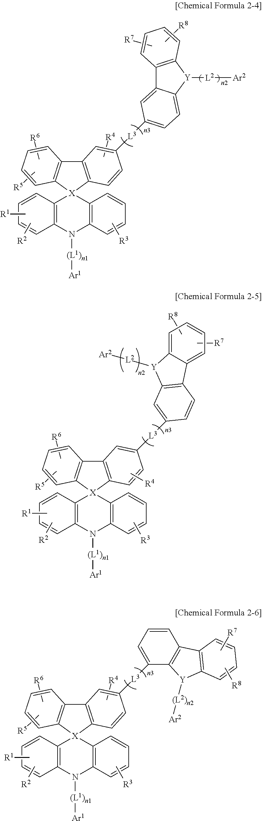


In the above Chemical Formulae 1-1 to 4-3,
X is C or Si,
Y is N, O or S,
R1 to R8 are independently hydrogen, deuterium, a halogen, a cyano group, a hydroxyl group, an amino group, a substituted or unsubstituted C1 to C20 amine group, a nitro group, a carboxyl group, a ferrocenyl group, a substituted or unsubstituted C1 to C20 alkyl group, a substituted or unsubstituted C6 to C30 aryl group, a substituted or unsubstituted C2 to C30 heteroaryl group, a substituted or unsubstituted C1 to C20 alkoxy group, a substituted or unsubstituted C6 to C20 aryloxy group, a substituted or unsubstituted C3 to C40 silyloxy group, a substituted or unsubstituted C1 to C20 acyl group, a substituted or unsubstituted C2 to C20 alkoxycarbonyl group, a substituted or unsubstituted C2 to C20 acyloxy group, a substituted or unsubstituted C2 to C20 acylamino group, a substituted or unsubstituted C2 to C20 alkoxycarbonylamino group, a substituted or unsubstituted C7 to C20 aryloxycarbonylamino group, a substituted or unsubstituted C1 to C20 sulfamoylamino group, a substituted or unsubstituted C1 to C20 sulfonyl group, a substituted or unsubstituted C1 to C20 alkylthiol group, a substituted or unsubstituted C6 to C20 arylthiol group, a substituted or unsubstituted C1 to C20 heterocyclothiol group, a substituted or unsubstituted C1 to C20 ureide group, a substituted or unsubstituted C3 to C40 silyl group, or a combination thereof,
L1 to L3 are independently a substituted or unsubstituted C2 to C6 alkenylene group, a substituted or unsubstituted C2 to C6 alkynylene group, a substituted or unsubstituted C6 to C30 arylene group, a substituted or unsubstituted C2 to C30 heteroarylene group, or a combination thereof,
n1 to n3 are independently integers of 0 to 3,
Ar1 and Ar2 are independently a substituted or unsubstituted C6 to C30 aryl group or a substituted or unsubstituted C2 to C30 heteroaryl group, and
at least one of Ar1, Ar2 and R8 is a substituted or unsubstituted C2 to C30 heteroaryl group having electron characteristics.
More specifically, in the various embodiments of the present invention (e.g., a compound represented by one of Chemical Formulae 1 to 4), the Ar1 is a substituted or unsubstituted C2 to C30 heteroaryl group having electron characteristics, and the Ar2 is a substituted or unsubstituted C6 to C30 aryl group. In this case, bipolar characteristics having separated electrons and holes characteristics, and thereby mobility of electrons and holes may be improved.
More specifically, in the various embodiments of the present invention (e.g., a compound represented by one of Chemical Formulae 1 to 4), the Ar2 is a substituted or unsubstituted C2 to C30 heteroaryl group having electron characteristics, and the Ar1 is a substituted or unsubstituted C6 to C30 aryl group. In this case, bipolar characteristics having separated electrons and holes characteristics, and thereby mobility of electrons and holes may be improved.
More specifically, the various embodiments of the present invention (e.g., a compound represented by one of Chemical Formulae 1 to 4), the substituted or unsubstituted C2 to C30 heteroaryl group having electron characteristics may be represented by one of the following Chemical Formulae 5 to 9, but is not limited thereto.

The compound has a relatively large molecular weight and thus, may be suppressed from decomposition during the deposition.
The L1 to L3 may be selectively adjusted to determine an entire conjugation length of the compound, and a triplet energy bandgap of the compound may be adjusted therefrom. Accordingly, characteristics of a material required of an organic photoelectric device may be realized. In addition, the triplet energy bandgap may also be adjusted by changing a bonding position of ortho, para, and meta.
Specific examples of the L1 to L3 may be a substituted or unsubstituted phenylene group, a substituted or unsubstituted biphenylene group, a substituted or unsubstituted terphenylene group, a substituted or unsubstituted naphthylene group, a substituted or unsubstituted anthracenylene group, a substituted or unsubstituted phenanthrylene group, a substituted or unsubstituted pyrenylene group, a substituted or unsubstituted fluorenylene group, a substituted or unsubstituted naphthacenyl group, a substituted or unsubstituted chrysenyl group, a substituted or unsubstituted triphenylenyl group, a substituted or unsubstituted perylenyl group, a substituted or unsubstituted indenyl group, a substituted or unsubstituted furanyl group, a substituted or unsubstituted thiophenyl group, a substituted or unsubstituted pyrrolyl group, a substituted or unsubstituted pyrazolyl group, a substituted or unsubstituted imidazolyl group, a substituted or unsubstituted triazolyl group, a substituted or unsubstituted oxazolyl group, a substituted or unsubstituted thiazolyl group, a substituted or unsubstituted oxadiazolyl group, a substituted or unsubstituted thiadiazolyl group, a substituted or unsubstituted pyridyl group, a substituted or unsubstituted pyrimidinyl group, a substituted or unsubstituted pyrazinyl group, a substituted or unsubstituted triazinyl group, a substituted or unsubstituted benzofuranyl group, a substituted or unsubstituted benzothiophenyl group, a substituted or unsubstituted benzimidazolyl group. substituted or unsubstituted indolyl group, a substituted or unsubstituted quinolinyl group, a substituted or unsubstituted isoquinolinyl group, a substituted or unsubstituted quinazolinyl group, a substituted or unsubstituted quinoxalinyl group, a substituted or unsubstituted naphthyridinyl group, a substituted or unsubstituted benzoxazinyl group, a substituted or unsubstituted benzthiazinyl group, a substituted or unsubstituted acridinyl group, a substituted or unsubstituted phenazinyl group, a substituted or unsubstituted phenothiazinyl group and a substituted or unsubstituted phenoxazinyl group.
In addition, the compound has steric hindrance and thus, small interaction among molecules and resultantly, may be suppressed from crystallization. Thereby, a yield of manufacturing a device may be improved. In addition, life-span characteristics of the device may be improved.
Furthermore, the compound has a relatively large molecular weight and thus, may be suppressed from decomposition during the deposition.
The Ar1 and Ar2 are independently, a substituted or unsubstituted phenyl group, a substituted or unsubstituted naphthyl group, a substituted or unsubstituted anthracenyl group, a substituted or unsubstituted phenanthryl group, a substituted or unsubstituted naphthacenyl group, a substituted or unsubstituted pyrenyl group, a substituted or unsubstituted biphenylyl group, a substituted or unsubstituted p-terphenyl group, a substituted or unsubstituted m-terphenyl group, a substituted or unsubstituted chrysenyl group, a substituted or unsubstituted triphenylenyl group, a substituted or unsubstituted perylenyl group, a substituted or unsubstituted indenyl group, a substituted or unsubstituted furanyl group, a substituted or unsubstituted thiophenyl group, a substituted or unsubstituted pyrrolyl group, a substituted or unsubstituted pyrazolyl group, a substituted or unsubstituted imidazolyl group, a substituted or unsubstituted triazolyl group, a substituted or unsubstituted oxazolyl group, a substituted or unsubstituted thiazolyl group, a substituted or unsubstituted oxadiazolyl group, a substituted or unsubstituted thiadiazolyl group, a substituted or unsubstituted pyridyl group, a substituted or unsubstituted pyrimidinyl group, a substituted or unsubstituted pyrazinyl group, a substituted or unsubstituted triazinyl group, a substituted or unsubstituted benzofuranyl group, a substituted or unsubstituted benzothiophenyl group, a substituted or unsubstituted benzimidazolyl group, a substituted or unsubstituted indolyl group, a substituted or unsubstituted quinolinyl group, a substituted or unsubstituted isoquinolinyl group, a substituted or unsubstituted quinazolinyl group, a substituted or unsubstituted quinoxalinyl group, a substituted or unsubstituted naphthyridinyl group, a substituted or unsubstituted benzoxazinyl group, a substituted or unsubstituted benzthiazinyl group, a substituted or unsubstituted acridinyl group, a substituted or unsubstituted phenazinyl group, a substituted or unsubstituted phenothiazinyl group, a substituted or unsubstituted phenoxazinyl group, or a combination thereof, but are not limited thereto.
More specifically, at least one of the Ar1 and Ar2 may be a substituted or unsubstituted biphenyl group.
In addition, at least one of the Ar1 and Ar2 may be a substituted or unsubstituted fluorenyl group.
More specifically, the substituted or unsubstituted phenyl group may be, for example, Chemical Formula S-57, and the like.

More specifically, the substituted or unsubstituted biphenyl group may be, for example, Chemical Formulae S-58, S-59 and S-60.

More specifically, the substituted or unsubstituted naphthyl group may be, for example, Chemical Formulae S-61 and S-62.

More specifically, the substituted or unsubstituted anthracenyl group may be, for example, Chemical Formulae S-63 and S-64.

More specifically, the substituted or unsubstituted phenanthrenyl group may be, for example, Chemical Formulae S-65, S-66, S-67, S-68 and S-69.

More specifically, the substituted or unsubstituted triphenyl group may be, for example, Chemical Formulae S-70 and S-71.

More specifically, the substituted or unsubstituted fluorenyl group may be, for example, Chemical Formulae S-72, S-73, S-74 and S-75.

At least one of the R1 to R8 may be a substituted or unsubstituted C3 to C40 silyl group.
The silyl group may lower a deposit temperature during manufacture of an organic optoelectronic device and increase solubility in a solvent and thus, convert a process of manufacturing a device into a solution process.
More specifically, at least one of the R1 to R8 may be a substituted C3 to C40 silyl group, and the substituted silyl group may be substituted with a C1 to C10 alkyl group or C6 to C15 aryl group, instead of at least one hydrogen of the silyl group.
Specific examples of the substituted silyl group may be a trimethylsilyl group, a triphenylsilyl group, and the like.
Specific examples of the compound for an organic optoelectronic device are the same as follows, but are not limited thereto.


The compound for an organic optoelectronic device has a maximum light emitting wavelength in a range of about 320 to about 520 nm and a triplet excited energy (T1) ranging from greater than or equal to about 2.0 eV, and specifically, from about 2.0 to about 4.0 eV, and thus may well transport a host charge having high triplet excited energy to a dopant and increase luminous efficiency of the dopant, and is also freely adjusted regarding HOMO and LUMO energy levels and decreases a driving voltage, and accordingly may be usefully applied as a host material or a charge transport material.
In addition, the compound for an organic optoelectronic device has photoactive and electrical activities, and thus may be usefully applied for a nonlinear optic material, an electrode material, a discolored material, a light switch, a sensor, a module, a wave guide, an organic transistor, a laser, a light absorbent, a dielectric material, a separating membrane, and the like.
The compound for an organic optoelectronic device including the compounds has a glass transition temperature of greater than or equal to 90° C. and a thermal decomposition temperature of greater than or equal to 400° C., indicating improved thermal stability. Thereby, it is possible to produce an organic optoelectronic device having high efficiency.
The compound for an organic optoelectronic device including the compounds may play a role of emitting light or injecting and/or transporting electrons, and may also act as a light emitting host with an appropriate dopantIn other words, the compound for an organic optoelectronic device may be used as a phosphorescent or fluorescent host material, a blue light emitting dopant material, or an electron transport material.
Since the compound for an organic optoelectronic device according to one embodiment is used for an organic thin layer, and it may improve the life-span characteristic, efficiency characteristic, electrochemical stability, and thermal stability of an organic optoelectronic device, and decrease the driving voltage.
Further, according to another embodiment, an organic optoelectronic device that includes the compound for an organic optoelectronic device is provided. The organic optoelectronic device may include an organic photoelectric device, an organic light emitting diode, an organic solar cell, an organic transistor, an organic photoconductor drum, an organic memory device, and the like. Particularly, the compound for an organic optoelectronic device according to one embodiment may be included in an electrode or an electrode buffer layer in an organic solar cell to improve the quantum efficiency, and it may be used as an electrode material for a gate, a source-drain electrode, or the like in the organic transistor.
Hereinafter, an organic light emitting diode is described.
According to another embodiment of the present invention, an organic light emitting diode includes an anode, a cathode, and at least one organic thin layer between the anode and the cathode, and at least one organic thin layer may include the compound for an organic optoelectronic device according to one embodiment of the present invention.
The organic thin layer that may include the compound for an organic optoelectronic device may include a layer selected from the group consisting of an emission layer, a hole transport layer (HTL), a hole injection layer (HIL), an electron transport layer (ETL), an electron injection layer (EIL), a hole blocking layer, and a combination thereof. The at least one layer includes the compound for an organic optoelectronic device according to one embodiment. Particularly, the compound for an organic optoelectronic device according to one embodiment may be included in a hole transport layer (HTL) or a hole injection layer (HIL). In addition, when the compound for an organic optoelectronic device is included in the emission layer, the compound for an organic optoelectronic device may be included as a phosphorescent or fluorescent host, and particularly, as a fluorescent blue dopant material.
Referring to FIG. 1 , an organic optoelectronic device 100 according to one embodiment includes an anode 120 and a cathode 110 facing each other and an organic layer 105 interposed between the anode 120 and cathode 110.
The anode 120 may be made of a conductor having a large work function to help hole injection, and may be for example metal, metal oxide and/or a conductive polymer. The anode 120 may be, for example a metal nickel, platinum, vanadium, chromium, copper, zinc, gold, and the like or an alloy thereof; metal oxide such as zinc oxide, indium oxide, indium tin oxide (ITO), indium zinc oxide (IZO), and the like; a combination of metal and oxide such as ZnO and Al or SnO2 and Sb; a conductive polymer such as poly(3-methylthiophene), poly(3,4-(ethylene-1,2-dioxy)thiophene) (PEDT), polypyrrole, and polyaniline, but is not limited thereto.
The cathode 110 may be made of a conductor having a small work function to help electron injection, and may be for example metal, metal oxide and/or a conductive polymer. The cathode 110 may be for example a metal or an alloy thereof such as magnesium, calcium, sodium, potassium, titanium, indium, yttrium, lithium, gadolinium, aluminum silver, tin, lead, cesium, barium, and the like; a multi-layer structure material such as LiF/Al, LiO2/Al, LiF/Ca, LiF/Al and BaF2/Ca, but is not limited thereto.
The organic layer 105 includes an emission layer 130 including the organic compound.
The emission layer 130 may include, for example the compound for an organic optoelectronic device at alone or with at least two of the compounds for an organic photoelectric device or as a mixture with other different compound from the compound for an organic optoelectronic device. When the compound for an organic optoelectronic device is mixed with the other compound, for example they may be included as a host and a dopant, wherein the compound for an organic optoelectronic device may be, for example included as a host. The host may be, for example phosphorescent host or fluorescent host, for example a phosphorescent host.
When the compound for an organic optoelectronic device is included as a host, the dopant may be selected from well-known inorganic, organic, organic/inorganic compound as a dopant.
Referring to FIG. 2 , an organic light emitting diode 200 further includes a hole auxiliary layer 140 as well as an emission layer 230. The hole auxiliary layer 140 may further increase hole injection and/or hole mobility between the anode 120 and emission layer 230 and block electrons. The hole auxiliary layer 140 may be, for example a hole transport layer (HTL), a hole injection layer (HIL), and/or an electron blocking layer, and may include at least one layer. The above organic compound may be included in the emission layer 230 and/or the hole auxiliary layer 140. In one embodiment of the present invention, an organic light emitting diode may further include an electron transport layer (ETL), an electron injection layer (EIL), a hole injection layer (HIL), and the like, as an organic thin layer 105 in FIG. 1 or FIG. 2 .
The organic light emitting diodes 100 and 200 may be manufactured by forming an anode or a cathode on a substrate, forming an organic layer in accordance with a dry coating method such as evaporation, sputtering, plasma plating, and ion plating; or a wet coating method such as spin coating, slit coating, dipping, flow coating and inkjet printing; and forming a cathode or an anode thereon.
The organic light emitting diode may be applied to a display device.
Hereinafter, the embodiments are illustrated in more detail with reference to examples. These examples, however, are not in any sense to be interpreted as limiting the scope of the invention.
(Preparation of Compound for Organic Optoelectronic Device)
A compound represented by the above Chemical Formula (A-1) as specific examples of a compound for an organic optoelectronic device according to the present invention was synthesized according to the following Reaction Scheme 1.


First Step; Synthesis of Compound (A)
30 g (120 mmol) of 2-bromo aniline, 38.8 g (150 mmol) of 1-chloro-3,5-phenyl triazine, and 7.3 g (300 mmol) of sodium hydride were agitated in 900 ml of dimethyl formaldehyde in a 2000 mL round flask at room temperature for 24 hours. After removing non-reaction sodium hydride by slowly dropping the reaction solution to distilled water, the reaction solution was poured into an excessive water of distilled water, and the mixture was filtered. The obtained solid was dissolved in an excessive amount of methylene chloride, the solution was hot-filtered, methylene chloride was removed therefrom again, and a solid obtained by precipitating the resultant in methanol was filtered, obtaining 40.5 g of a compound (A) (a yield of 70%).
The elemental analysis result of the compound (A) was provided as follows.
calcd. C27H19BrN4: C, 67.65; H, 4.00; Br, 16.67; N, 11.69. found: C, 67.35; H, 4.03; N, 10.88.
Second Step: Synthesis of Compound (C)
30 g (62.5 mmol) of the compound (A) was put in a 500 mL round flask and dissolved in 300 mL of tetrahydrofuran after making its reaction atmosphere be in a nitrogen state, and a temperature around a reactor was maintained at −78° C. Then, 25 mL of 2.5 M-normal butyl lithium was slowly added thereto in a dropwise fashion. When the addition was complete, the mixture was agitated for 30 minutes, and a solution obtained by dissolving 16.2 g (62.5 mmol) of 2-bromo fluoreneol in 200 mL of purified tetrahydrofuran was slowly added thereto. The reaction solution was agitated for about one hour while maintained at −78° C. and then, heated up to room temperature and kept being agitated until the next day morning. After completing a reaction by adding a 5 wt % sodium bicarbonate aqueous solution to the reaction solution, the resultant was separately extracted by using methylene chloride. The obtained organic layer was distilled under a reduced pressure after removing water remaining there with magnesium sulfate, obtaining an intermediate (B). The unpurified intermediate (B) was put in 400 mL of acetic acid, hydrochloric acid in a catalyst amount was added thereto, and the mixture was agitated for 12 hours at a reflux temperature. When the reaction was complete, 24 g of a compound (C) was obtained through column chromatography (a yield of 62%).
The elemental analysis result of the compound (C) was provided as follows.
calcd. C40H25BrN4: C, 74.88; H, 3.93; Br, 12.45; N, 8.73. found: C, 74.65; H, 3.91; N, 8.75
Third Step: Synthesis of Compound (A-1)
20 g (31.1 mmol) of the compound (C), 11.5 g (31.1 mmol) of a 3-(4,4,5,5-tetramethyl-1,3,2-dioxaborane-N-phenyl-carbazole compound and 1.8 g (1.2 mmol) of tetrakis triphenyl phosphine were suspended in 400 ml of toluene/tetrahydrofuran, 400 ml of a 2 M potassium carbonate aqueous solution was added thereto, and the mixture was heated and refluxed under a nitrogen stream for 24 hours. The reaction solution was added to 2000 ml of MeOH, a crystallized solid therein was filtered and dissolved in monochlorobenzene, and the solution was filtered with silica gel/Celite. After removing an organic solvent in an appropriate amount therefrom, the resultant was recrystallized in MeOH, obtaining 11.4 g of a compound (A-1) (a yield of 50%).
The elemental analysis result of the compound (A-1) was provided as follows.
calcd. C58H37N5: C, 86.65; H, 4.64; N, 8.71. found: C, 86.71; H, 4.64; N, 8.75
A compound represented by the above Chemical Formula (A-6) as specific examples of a compound for an organic optoelectronic device of the present invention was synthesized according to the following Reaction Scheme 2.


First Step; Synthesis of Compound (A-6)
20 g (31.1 mmol) of the compound (C) synthesized through the first and second steps in Example 1, 6.6 g (31.1 mmol) of a 4-boronic acid-dibenzo furan compound and 1.8 g (1.2 mmol) of tetrakis triphenyl phosphine were suspended in 400 ml of toluene/tetrahydrofuran, 400 ml of a 2 M potassium carbonate aqueous solution was added thereto, and the mixture was heated and refluxed under a nitrogen stream for 24 hours. The reaction solution was added to 2000 ml of MeOH, a crystallized solid therein was filtered and dissolved in monochlorobenzene, and the solution was filtered with silica gel/Celite. After removing an organic solvent in an appropriate amount therefrom, the resultant was recrystallized in MeOH, obtaining 11.4 g of a compound (A-6) (a yield of 50%).
The elemental analysis result of the compound (A-6) was provided as follows.
calcd. C52H32N4O: C, 85.69; H, 4.43; N, 7.69; O, 2.20. found: C, 85.69; H, 4.43; N, 7.69
A compound represented by the above Chemical Formula (A-26) as specific examples of a compound for an organic optoelectronic device of the present invention was synthesized according to the following Reaction Scheme 3.


First Step; Synthesis of Compound (D)
30 g (120 mmol) of 2-bromo aniline, 38.8 g (150 mmol) of 1-chloro-3,5-phenyl pyrimidine, and 7.3 g (300 mmol) of sodium hydride were put in 900 ml of dimethyl formaldehyde in a 2000 mL round flask, and the mixture was agitated at room temperature for 24 hours. After removing non-reaction sodium hydride by slowly dropping the reaction solution to distilled water, the reaction solution was poured into an excessive amount of distilled water again, and then, the mixture was filtered. The obtained solid was dissolved in an excessive amount of methylene chloride, the solution was hot-filtered, methylene chloride was removed therefrom again, and a solid obtained by precipitating the resultant in methanol was filtered, obtaining 36.5 g of a compound (D) (a yield of 66%).
The elemental analysis result of the compound (D) was provided as follows.
calcd. C28H20BrN3: C, 70.30; H, 4.21; Br, 16.70; N, 8.78. found: C, 70.32; H, 4.20; N, 8.90
Second Step: Synthesis of Compound (F)
30 g (62.5 mmol) of the compound (D) was put in a 500 mL round flask and then, dissolved in 300 mL of purified tetrahydrofuran after making its reaction atmosphere be in a nitrogen state, and a temperature around a reactor was maintained at −78° C. Then, 25 mL of 2.5 M-normal butyl lithium was slowly added thereto in a dropwise fashion. When the addition was complete, the mixture was agitated for 30 minutes, and a solution obtained by dissolving 16.2 g (62.5 mmol) of 2-bromo fluoreneol in 200 mL of purified tetrahydrofuran was slowly added thereto. The reaction solution was agitated for about one hour while maintained at −78° C. and then, heated up to room temperature and kept being agitated until the next day morning. After completing the reaction by adding a 5 wt % sodium bicarbonate aqueous solution to the reaction solution, the mixture was separately extracted by using methylene chloride. The obtained organic layer was distilled under a reduced pressure after removing water remaining there by using magnesium sulfate, obtaining an intermediate (E). The unpurified intermediate (E) was put in 400 mL of acetic acid, hydrochloric acid in a catalyst amount was added thereto, and the mixture was agitated at a reflux temperature for 12 hours. When the reaction was complete, 28 g of a compound (F) was obtained through column chromatography (a yield of 64%).
The elemental analysis result of the compound (F) was provided as follows.
calcd. C41H26BrN3: C, 76.88; H, 4.09; Br, 12.47; N, 6.56. found: C, 76.72; H, 4.15; N, 6.61
Third Step: Synthesis of Compound (A-26)
20 g (31.1 mmol) of the compound (F), 11.5 g (31.1 mmol) of a 3-(4,4,5,5-tetramethyl-1,3,2-dioxaborane-N-phenyl-carbazole compound and 1.8 g (1.2 mmol) of tetrakis triphenyl phosphine were suspended in 400 ml of toluene/tetrahydrofuran, 400 ml of a 2 M potassium carbonate aqueous solution were added thereto, and the mixture was heated and refluxed under a nitrogen stream for 24 hours. The reaction solution was added to 2000 ml of MeOH, a crystallized solid therein was filtered and dissolved in monochlorobenzene, and the solution was filtered with silica gel/Celite. After removing an organic solvent in an appropriate amount therefrom, the resultant was recrystallized with MeOH, obtaining 13 g of a compound (A-26) (a yield of 55%).
The elemental analysis result of the compound (A-26) was provided as follows.
calcd. C59H38N4: C, 88.25; H, 4.77; N, 6.98. found: C, 88.21; H, 4.69; N, 7.01
A compound represented by the above Chemical Formula A-36 as specific examples of a compound for an organic optoelectronic device of the present invention was synthesized through the following Reaction Scheme 4.


First Step; Synthesis of Compound (A-36)
20 g (31.1 mmol) of the compound (F) synthesized through the steps 1 and 2 in Example 3, 6.6 g (31.1 mmol) of a 4-boronic acid-dibenzo furan compound and 1.8 g (1.2 mmol) of tetrakis triphenyl phosphine were suspended in 400 ml of toluene/tetrahydrofuran, 400 ml of a 2 M potassium carbonate aqueous solution was added thereto, and the mixture was heated and refluxed under a nitrogen stream for 24 hours. The reaction solution was added to 2000 ml of MeOH, a crystallized solid therein was filtered and dissolved in monochlorobenzene, and then, the solution was filtered with silica gel/Celite. After removing an organic solvent in an appropriate amount therefrom, the resultant was recrystallized with MeOH, obtaining 14 g of a compound A-36 (a yield of 60%).
The elemental analysis result of the compound A-36 was provided as follows.
calcd. C53H33N3O: C, 87.46; H, 4.57; N, 5.77; O, 2.20. found: C, 87.36; H, 4.60; N, 5.77
A compound represented by the above Chemical Formula A-22 as specific examples of a compound for an organic optoelectronic device of the present invention was synthesized according to the following Reaction Scheme 5.


First Step; Synthesis of Compound (H)
30 g (62.5 mmol) of the compound (A) synthesized through the step 1 of Example 1 was put in a 500 mL round flask and then, dissolved in 300 mL of purified tetrahydrofuran after making its reaction atmosphere be in a nitrogen state, and then, a temperature around a reactor was maintained at −78° C. Then, 25 mL of 2.5 M-normal butyl lithium was slowly added thereto in a dropwise fashion. When the addition was complete, the mixture was agitated for 30 minutes, and a solution obtained by dissolving 16.2 g (62.5 mmol) of 3-bromo benzophenone in 200 mL of purified tetrahydrofuran was slowly added thereto in a dropwise fashion. The reaction solution was agitated for about 1 hour while maintained at about −78° C. and then, heated up to room temperature and kept being agitated until the next day morning. After completing the reaction by adding a 5 wt % sodium bicarbonate aqueous solution thereto, the mixture was separately extracted by using methylene chloride. The obtained organic layer therefrom was distilled under a reduced pressure after removing water remaining therein by using magnesium sulfate, obtaining an intermediate (G). The unpurified intermediate (G) was put in 400 mL of acetic acid, hydrochloric acid in a catalyst amount was added thereto, and the mixture was agitated at a reflux temperature for 12 hours. When the reaction was complete, 24 g of a compound (H) was obtained through column chromatography (a yield of 62%).
The elemental analysis result of the compound (H) was provided as follows.
calcd. C40H27BrN4: C, 74.65; H, 4.23; Br, 12.42; N, 8.71. found: C, 74.67; H, 4.21; N, 8.72
Second Step: Synthesis of Compound (A-22)
20 g (31.1 mmol) of the compound (H), 11.5 g (31.1 mmol) of a 3-(4,4,5,5-tetramethyl-1,3,2-dioxaborane-N-phenyl-carbazole compound and 1.8 g (1.2 mmol) of tetrakis triphenyl phosphine were suspended in 400 ml of toluene/tetrahydrofuran, 400 ml of a 2 M potassium carbonate aqueous solution was added thereto, and the mixture was heated and refluxed under a nitrogen stream for 24 hours. The reaction solution was added to 2000 ml of MeOH, a crystallized solid therein was filtered and dissolved in monochlorobenzene, and the solution was filtered with silica gel/Celite. After removing an organic solvent in an appropriate amount therefrom, the resultant was recrystallized with MeOH, obtaining 11 g of a compound (A-22) (a yield of 49%).
The elemental analysis result of the compound (A-22) was provided as follows.
calcd. C58H39N5: C, 86.43; H, 4.88; N, 8.69. found: C, 86.41; H, 4.88; N, 8.72
A compound represented by the above Chemical Formula A-111 as specific examples of a compound for an organic optoelectronic device of the present invention was synthesized according to the same method as the following Reaction Scheme 6.


First Step; Synthesis of Compound (A-111)
20 g (31.1 mmol) of the compound (H) synthesized through the steps 1 and 2 in Example 5, 6.6 g (31.1 mmol) of a 4-boronic acid-dibenzo furan compound and 1.8 g (1.2 mmol) of tetrakis triphenyl phosphine were suspended in 400 ml of toluene/tetrahydrofuran, 400 ml of a 2 M potassium carbonate aqueous solution was added thereto, and the mixture was heated and refluxed under a nitrogen stream for 24 hours. The reaction solution was added to 2000 ml of MeOH, a crystallized solid therein was filtered and dissolved in monochlorobenzene, and the solution was filtered with silica gel/Celite. After removing an organic solvent in an appropriate amount therefrom, the resultant was recrystallized with MeOH, obtaining 12 g of a compound (A-111) (a yield of 54%).
The elemental analysis result of the compound (A-111) was provided as follows.
calcd. C52H34N4O: C, 85.46; H, 4.69; N, 7.67; O, 2.19. found: C, 85.49; H, 4.65; N, 7.61
A compound represented by the above Chemical Formula A-92 as specific examples of a compound for an organic optoelectronic device of the present invention was synthesized through the following Reaction Scheme 7.


First Step; Synthesis of Compound (J)
30 g (62.5 mmol) of the compound (D) synthesized through the step 1 of Example 3 was put in a 500 mL round flask and then, dissolved in 300 mL of purified tetrahydrofuran after making the reaction atmosphere be in a nitrogen state, and a temperature around a reactor was maintained at −78° C. Then, 25 mL of a 2.5 M-normal butyl lithium was slowly added thereto in a dropwise fashion. When the addition was complete, the mixture was agitated for 30 minutes, a solution obtained by dissolving 16.2 g (62.5 mmol) of 3-bromo benzophenone in 200 mL of tetrahydrofuran was slowly added thereto. The reaction solution was agitated for about 1 hour while maintained at −78° C. and then, heated up to room temperature and kept being agitated until the next day morning. After completing the reaction by adding a 5 wt % sodium bicarbonate aqueous solution to the reaction solution, the resultant was separately extracted by using methylene chloride. The obtained organic layer was distilled under a reduced pressure after removing water remaining there by using magnesium sulfate, obtaining an intermediate (I). The unpurified intermediate (I) was put in 400 mL of acetic acid, hydrochloric acid in a catalyst amount was added thereto, and the mixture was agitated for 12 hours at a reflux temperature. When the reaction was complete, 25 g of a compound (J) was obtained through column chromatography (a yield of 59%).
The elemental analysis result of the compound (J) was provided as follows.
calcd. C41H28BrN3: C, 76.63; H, 4.39; Br, 12.43; N, 6.54. found: C, 76.63; H, 4.36; N, 6.55
Second Step: Synthesis of Compound (A-92)
20 g (31.1 mmol) of the compound (J), 11.5 g (31.1 mmol) of a 3-(4,4,5,5-tetramethyl-1,3,2-dioxaborane-N-phenyl-carbazole compound and 1.8 g (1.2 mmol) of tetrakis triphenyl phosphine were suspended in 400 ml of toluene/tetrahydrofuran, 400 ml of a 2 M potassium carbonate aqueous solution was added thereto, and the mixture was heated and refluxed under a nitrogen stream for 24 hours. The reaction solution was added to 2000 ml of MeOH, a crystallized solid was filtered therefrom and dissolved in monochlorobenzene, and the solution was filtered with silica gel/Celite. After removing an organic solvent in an appropriate amount therefrom, the resultant was recrystallized with MeOH, obtaining 13 g of a compound (A-26) (a yield of 55%).
The elemental analysis result of the compound (A-92) was provided as follows.
calcd. C59H40N4: C, 88.03; H, 5.01; N, 6.96. found: C, 88.02; H, 5.00; N, 6.96
A compound represented by the above Chemical Formula A-114 as specific examples of a compound for an organic optoelectronic device of the present invention was synthesized according to the following Reaction Scheme 8.


First Step; Synthesis of Compound (A-114)
20 g (31.1 mmol) of the compound (J) synthesized through the steps 1 and 2 in Example 7, 6.6 g (31.1 mmol) of a 4-boronic acid-dibenzo furan compound and 1.8 g (1.2 mmol) of tetrakis triphenyl phosphine were suspended in 400 ml of toluene/tetrahydrofuran, 400 ml of a 2 M potassium carbonate aqueous solution was added thereto, and the mixture was heated and refluxed under a nitrogen stream for 24 hours. The reaction solution was added to 2000 ml of MeOH, a crystallized solid was filtered therefrom and dissolved in monochlorobenzene, and the solution was filtered with silica gel/Celite. After removing an organic solvent in an appropriate amount therefrom, the resultant was recrystallized with MeOH, obtaining 17 g of a compound (A-114) (a yield of 65%).
The elemental analysis result of the compound (A-114) was provided as follows.
calcd. C53H35N3O: C, 87.22; H, 4.83; N, 5.76; O, 2.19. found: C, 87.21; H, 4.83; N, 5.77
(Manufacture of Organic Light Emitting Diode)
Specifically, illustrating a method of manufacturing an organic light emitting diode, an anode was manufactured by cutting an ITO glass substrate having a sheet resistance of 15 Ω/cm2 into a size of 50 mm×50 mm×0.7 mm, respectively ultrasonic wave-cleaning it in acetone, isopropylalcohol and pure water for 15 minutes and then, UV ozone-cleaning it for 30 minutes.
This obtained ITO transparent electrode was used as an anode, and a 1200 Å-thick hole injection layer (HIL) was formed on the ITO substrate by vacuum-depositing the following HTM compound.

Then, the compound synthesized in Example 1 as a host and 7 wt % of the following PhGD compound as a phosphorescent green dopant were vacuum-deposited to form a 300 Å-thick emission layer. As for an anode, 1000 Å-thick aluminum (Al) was used, while 1000 Å-thick ITO was used as for a cathode.

Then, on the emission layer, 50 Å-thick BAlq [bis(2-methyl-8-quinolinolato-N1,O8)-(1,1′-Biphenyl-4-olato)aluminum] and 250 Å-thick Alq3 [tris(8-hydroxyquinolinato)aluminium] were sequentially accumulated to form an electron transport layer (ETL). On the electron transport layer (ETL), 5 Å-thick LiF and 1000 Å-thick Al were sequentially vacuum-deposit to form a cathode, manufacturing an organic light emitting diode.

An organic light emitting diode was manufactured according to the same method as Example 9 except for using the compound of Example 2 instead of the compound of Example 1 in Example 9.
An organic light emitting diode was manufactured according to the same method as Example 9 except for using the compound of Example 3 instead of the compound of Example 1 in Example 9.
An organic light emitting diode was manufactured according to the same method as Example 9 except for using 4,4-N,N-dicarbazolebiphenyl (CBP) instead of the compound synthesized in Example 1 as the host for the emission layer in Example 9.
(Performance Measurement of Organic Light Emitting Diode)
Current density change, luminance change, and luminous efficiency of each organic light emitting diode according to the Examples 9 to 11 and Comparative Example 1 depending on a voltage were measured. Specific measurement methods are as follows, and the results are shown in the following Table 1.
(1) Measurement of Current Density Change Depending on Voltage Change
The obtained organic light emitting diodes were measured for current value flowing in the unit device while increasing the voltage from 0 V to 10 V using a current-voltage meter (Keithley 2400), the measured current value was divided by area to provide the results.
(2) Measurement of Luminance Change Depending on Voltage Change
Luminance was measured by using a luminance meter (Minolta Cs-1000A), while the voltage of the organic light emitting diodes was increased from 0 V to 10 V.
(3) Measurement of Luminous Efficiency
The luminance, current density, and voltage obtained from the (1) and (2) were used to calculate current efficiency (cd/A) at the same current density (10 mA/cm2).
| TABLE 1 | |||||||
| Driving | Current | Power | Color | Color | |||
| voltage | efficiency | efficiency | Luminance | coordinate | coordinate | ||
| (Vd, V) | (cd/A) | (lm/W) | (cd/m2) | (CIEx) | (CIEy) | ||
| Comparative | 4.02 | 36.9 | 34 | 3000 | 0.340 | 0.627 |
| Example 1 | ||||||
| Example 9 | 4.05 | 39.1 | 38.2 | 3000 | 0.350 | 0.618 |
| Example 10 | 4.15 | 38.6 | 37.9 | 3000 | 0.350 | 0.620 |
| Example 11 | 4.09 | 41.2 | 40.2 | 3000 | 0.350 | 0.619 |
The organic light emitting diodes of Examples 6 to 7 showed improved efficiency compared with the organic light emitting diodes of Comparative Example 1 using CBP as the host for the emission layer.
Example embodiments have been disclosed herein, and although specific terms are employed, they are used and are to be interpreted in a generic and descriptive sense only and not for purpose of limitation. In some instances, as would be apparent to one of ordinary skill in the art as of the filing of the present application, features, characteristics, and/or elements described in connection with a particular embodiment may be used singly or in combination with features, characteristics, and/or elements described in connection with other embodiments unless otherwise specifically indicated. Accordingly, it will be understood by those of skill in the art that various changes in form and details may be made without departing from the spirit and scope of the present invention as set forth in the following claims.
Claims (14)
1. A compound for an organic optoelectronic device, the compound comprising moieties represented by the following Chemical Formula I and Chemical Formula II, the moieties represented by Chemical Formula I and Chemical Formula II being sequentially linked:

wherein, in Chemical Formula I and Chemical Formula II,
--- indicates a single bond or no bond,
* indicates a binding point of Chemical Formula I and Chemical Formula II wherein Chemical Formula I is linked to Chemical Formula II at one * of the two *s of Chemical Formula I,
X is C or Si,
Y is N, O, or S,
R1 to R8 are each independently hydrogen, deuterium, a halogen, a cyano group, a hydroxyl group, an amino group, a substituted or unsubstituted C1 to C20 amine group, a nitro group, a carboxyl group, a ferrocenyl group, a substituted or unsubstituted C1 to C20 alkyl group, a substituted or unsubstituted C6 to C30 aryl group, a substituted or unsubstituted C2 to C30 heteroaryl group, a substituted or unsubstituted C1 to C20 alkoxy group, a substituted or unsubstituted C6 to C20 aryloxy group, a substituted or unsubstituted C3 to C40 silyloxy group, a substituted or unsubstituted C1 to C20 acyl group, a substituted or unsubstituted C2 to C20 alkoxycarbonyl group, a substituted or unsubstituted C2 to C20 acyloxy group, a substituted or unsubstituted C2 to C20 acylamino group, a substituted or unsubstituted C2 to C20 alkoxycarbonylamino group, a substituted or unsubstituted C7 to C20 aryloxycarbonylamino group, a substituted or unsubstituted C1 to C20 sulfamoylamino group, a substituted or unsubstituted C1 to C20 sulfonyl group, a substituted or unsubstituted C1 to C20 alkylthiol group, a substituted or unsubstituted C6 to C20 arylthiol group, a substituted or unsubstituted C1 to C20 heterocyclothiol group, a substituted or unsubstituted C1 to C20 ureide group, a substituted or unsubstituted C3 to C40 silyl group, or a combination thereof,
L1 to L3 are each independently a substituted or unsubstituted C2 to C6 alkenylene group, a substituted or unsubstituted C2 to C6 alkynylene group, a substituted or unsubstituted C6 to C30 arylene group, a substituted or unsubstituted C2 to C30 heteroarylene group, or a combination thereof,
n1 to n3 are each independently integers of 0 to 3,
Ar1 and Ar2 are each independently a substituted or unsubstituted C6 to C30 aryl group or a substituted or unsubstituted C2 to C30 heteroaryl group, and
at least one of Ar1, Ar2, and R8 is a substituted or unsubstituted C2 to C30 heteroaryl group having electron characteristics.
2. The compound for an organic optoelectronic device as claimed in claim 1 , wherein the compound is represented by one of the following Chemical Formula 1 to Chemical Formula 4:

wherein, in Chemical Formula 1 to Chemical Formula 4,
X is C or Si,
Y is N, O, or S,
R1 to R8 are each independently hydrogen, deuterium, a halogen, a cyano group, a hydroxyl group, an amino group, a substituted or unsubstituted C1 to C20 amine group, a nitro group, a carboxyl group, a ferrocenyl group, a substituted or unsubstituted C1 to C20 alkyl group, a substituted or unsubstituted C6 to C30 aryl group, a substituted or unsubstituted C2 to C30 heteroaryl group, a substituted or unsubstituted C1 to C20 alkoxy group, a substituted or unsubstituted C6 to C20 aryloxy group, a substituted or unsubstituted C3 to C40 silyloxy group, a substituted or unsubstituted C1 to C20 acyl group, a substituted or unsubstituted C2 to C20 alkoxycarbonyl group, a substituted or unsubstituted C2 to C20 acyloxy group, a substituted or unsubstituted C2 to C20 acylamino group, a substituted or unsubstituted C2 to C20 alkoxycarbonylamino group, a substituted or unsubstituted C7 to C20 aryloxycarbonylamino group, a substituted or unsubstituted C1 to C20 sulfamoylamino group, a substituted or unsubstituted C1 to C20 sulfonyl group, a substituted or unsubstituted C1 to C20 alkylthiol group, a substituted or unsubstituted C6 to C20 arylthiol group, a substituted or unsubstituted C1 to C20 heterocyclothiol group, a substituted or unsubstituted C1 to C20 ureide group, a substituted or unsubstituted C3 to C40 silyl group, or a combination thereof,
L1 to L3 are each independently a substituted or unsubstituted C2 to C6 alkenylene group, a substituted or unsubstituted C2 to C6 alkynylene group, a substituted or unsubstituted C6 to C30 arylene group, a substituted or unsubstituted C2 to C30 heteroarylene group, or a combination thereof,
n1 to n3 are each independently integers of 0 to 3,
Ar1 and Ar2 are each independently a substituted or unsubstituted C6 to C30 aryl group or a substituted or unsubstituted C2 to C30 heteroaryl group, and
at least one of Ar1, Ar2, and R8 is a substituted or unsubstituted C2 to C30 heteroaryl group having electron characteristics.
3. The compound for an organic optoelectronic device as claimed in claim 1 , wherein the compound is represented by one of the following Chemical Formula 1-1 to Chemical Formula 4-3:


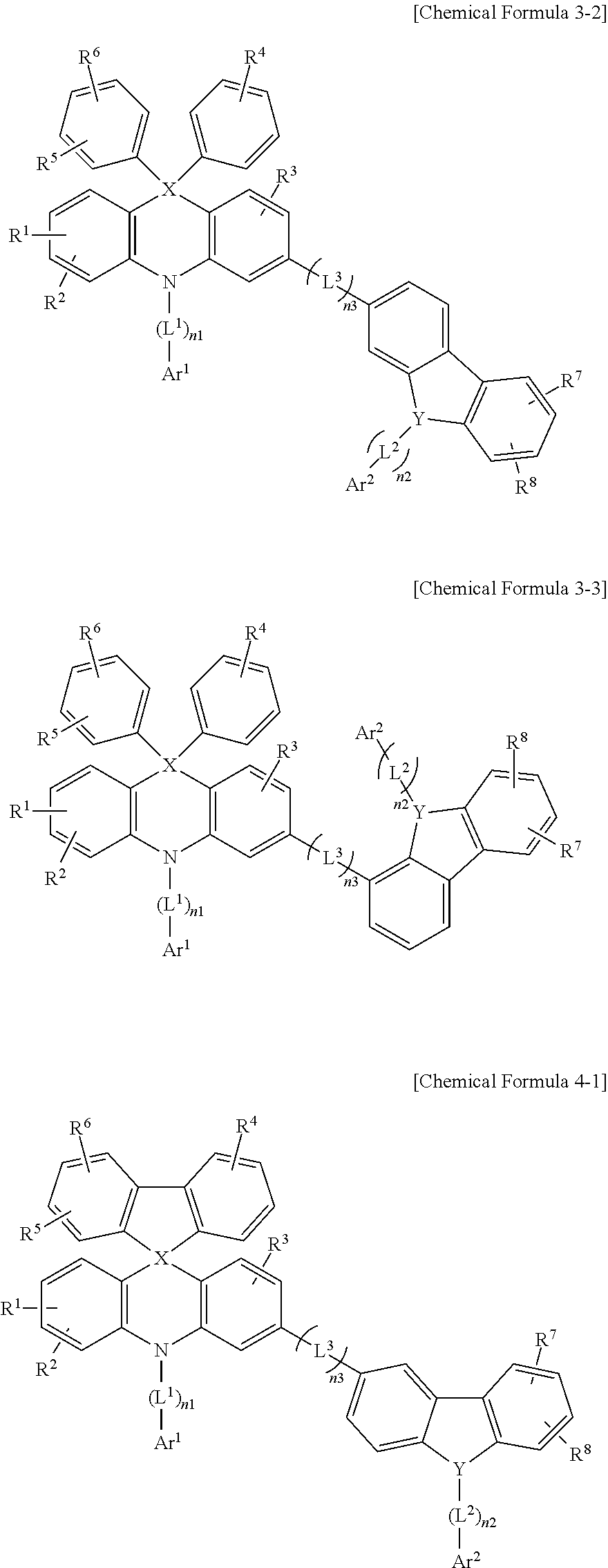

wherein, in Chemical Formula 1-1 to Chemical Formula 4-3,
X is C or Si,
Y is N, O, or S,
R1 to R8 are each independently hydrogen, deuterium, a halogen, a cyano group, a hydroxyl group, an amino group, a substituted or unsubstituted C1 to C20 amine group, a nitro group, a carboxyl group, a ferrocenyl group, a substituted or unsubstituted C1 to C20 alkyl group, a substituted or unsubstituted C6 to C30 aryl group, a substituted or unsubstituted C2 to C30 heteroaryl group, a substituted or unsubstituted C1 to C20 alkoxy group, a substituted or unsubstituted C6 to C20 aryloxy group, a substituted or unsubstituted C3 to C40 silyloxy group, a substituted or unsubstituted C1 to C20 acyl group, a substituted or unsubstituted C2 to C20 alkoxycarbonyl group, a substituted or unsubstituted C2 to C20 acyloxy group, a substituted or unsubstituted C2 to C20 acylamino group, a substituted or unsubstituted C2 to C20 alkoxycarbonylamino group, a substituted or unsubstituted C7 to C20 aryloxycarbonylamino group, a substituted or unsubstituted C1 to C20 sulfamoylamino group, a substituted or unsubstituted C1 to C20 sulfonyl group, a substituted or unsubstituted C1 to C20 alkylthiol group, a substituted or unsubstituted C6 to C20 arylthiol group, a substituted or unsubstituted C1 to C20 heterocyclothiol group, a substituted or unsubstituted C1 to C20 ureide group, a substituted or unsubstituted C3 to C40 silyl group, or a combination thereof,
L1 to L3 are each independently a substituted or unsubstituted C2 to C6 alkenylene group, a substituted or unsubstituted C2 to C6 alkynylene group, a substituted or unsubstituted C6 to C30 arylene group, a substituted or unsubstituted C2 to C30 heteroarylene group, or a combination thereof,
n1 to n3 are each independently integers of 0 to 3,
Ar1 and Ar2 are each independently a substituted or unsubstituted C6 to C30 aryl group or a substituted or unsubstituted C2 to C30 heteroaryl group, and
at least one of Ar1, Ar2, and R8 is a substituted or unsubstituted C2 to C30 heteroaryl group having electron characteristics.
4. The compound for an organic optoelectronic device as claimed in claim 1 , wherein:
Ar1 is a substituted or unsubstituted C2 to C30 heteroaryl group having electron characteristics, and
Ar2 is a substituted or unsubstituted C6 to C30 aryl group.
5. The compound for an organic optoelectronic device as claimed in claim 1 , wherein:
Ar2 is a substituted or unsubstituted C2 to C30 heteroaryl group having electron characteristics, and
Ar1 is a substituted or unsubstituted C6 to C30 aryl group.
6. The compound for an organic optoelectronic device as claimed in claim 1 , wherein the substituted or unsubstituted C2 to C30 heteroaryl group having electron characteristics is a group represented by one of the following Chemical Formulae 5 to 9:

in which * represents a binding site to a neighboring atom.
7. The compound for an organic optoelectronic device as claimed in claim 1 , wherein Ar1 and Ar2 are each independently a substituted or unsubstituted phenyl group, a substituted or unsubstituted naphthyl group, a substituted or unsubstituted anthracenyl group, a substituted or unsubstituted phenanthryl group, a substituted or unsubstituted naphthacenyl group, a substituted or unsubstituted pyrenyl group, a substituted or unsubstituted biphenylyl group, a substituted or unsubstituted p-terphenyl group, a substituted or unsubstituted m-terphenyl group, a substituted or unsubstituted chrysenyl group, a substituted or unsubstituted triphenylenyl group, a substituted or unsubstituted perylenyl group, a substituted or unsubstituted indenyl group, a substituted or unsubstituted furanyl group, a substituted or unsubstituted thiophenyl group, a substituted or unsubstituted pyrrolyl group, a substituted or unsubstituted pyrazolyl group, a substituted or unsubstituted imidazolyl group, a substituted or unsubstituted triazolyl group, a substituted or unsubstituted oxazolyl group, a substituted or unsubstituted thiazolyl group, a substituted or unsubstituted oxadiazolyl group, a substituted or unsubstituted thiadiazolyl group, a substituted or unsubstituted pyridyl group, a substituted or unsubstituted pyrimidinyl group, a substituted or unsubstituted pyrazinyl group, a substituted or unsubstituted triazinyl group, a substituted or unsubstituted benzofuranyl group, a substituted or unsubstituted benzothiophenyl group, a substituted or unsubstituted benzimidazolyl group, a substituted or unsubstituted indolyl group, a substituted or unsubstituted quinolinyl group, a substituted or unsubstituted isoquinolinyl group, a substituted or unsubstituted quinazolinyl group, a substituted or unsubstituted quinoxalinyl group, a substituted or unsubstituted naphthyridinyl group, a substituted or unsubstituted benzoxazinyl group, a substituted or unsubstituted benzthiazinyl group, a substituted or unsubstituted acridinyl group, a substituted or unsubstituted phenazinyl group, a substituted or unsubstituted phenothiazinyl group, a substituted or unsubstituted phenoxazinyl group, or a combination thereof.
8. The compound for an organic optoelectronic device as claimed in claim 1 , wherein L1 to L3 are each independently a substituted or unsubstituted phenylene group, a substituted or unsubstituted biphenylene group, a substituted or unsubstituted terphenylene group, a substituted or unsubstituted naphthylene group, a substituted or unsubstituted anthracenylene group, a substituted or unsubstituted phenanthrylene group, a substituted or unsubstituted pyrenylene group, a substituted or unsubstituted fluorenylene group, a substituted or unsubstituted naphthacenyl group, a substituted or unsubstituted chrysenyl group, a substituted or unsubstituted triphenylenyl group, a substituted or unsubstituted perylenyl group, a substituted or unsubstituted indenyl group, a substituted or unsubstituted furanyl group, a substituted or unsubstituted thiophenyl group, a substituted or unsubstituted pyrrolyl group, a substituted or unsubstituted pyrazolyl group, a substituted or unsubstituted imidazolyl group, a substituted or unsubstituted triazolyl group, a substituted or unsubstituted oxazolyl group, a substituted or unsubstituted thiazolyl group, a substituted or unsubstituted oxadiazolyl group, a substituted or unsubstituted thiadiazolyl group, a substituted or unsubstituted pyridyl group, a substituted or unsubstituted pyrimidinyl group, a substituted or unsubstituted pyrazinyl group, a substituted or unsubstituted triazinyl group, a substituted or unsubstituted benzofuranyl group, a substituted or unsubstituted benzothiophenyl group, a substituted or unsubstituted benzimidazolyl group. substituted or unsubstituted indolyl group, a substituted or unsubstituted quinolinyl group, a substituted or unsubstituted isoquinolinyl group, a substituted or unsubstituted quinazolinyl group, a substituted or unsubstituted quinoxalinyl group, a substituted or unsubstituted naphthyridinyl group, a substituted or unsubstituted benzoxazinyl group, a substituted or unsubstituted benzthiazinyl group, a substituted or unsubstituted acridinyl group, a substituted or unsubstituted phenazinyl group, a substituted or unsubstituted phenothiazinyl group and a substituted or unsubstituted phenoxazinyl group.
9. The compound for an organic optoelectronic device as claimed in claim 1 , wherein at least one of R1 to R8 is a substituted or unsubstituted C3 to C40 silyl group.
10. The compound for an organic optoelectronic device as claimed in claim 1 , wherein the compound is one selected from Compounds A-1 to A-117 and B-1 to B-60:


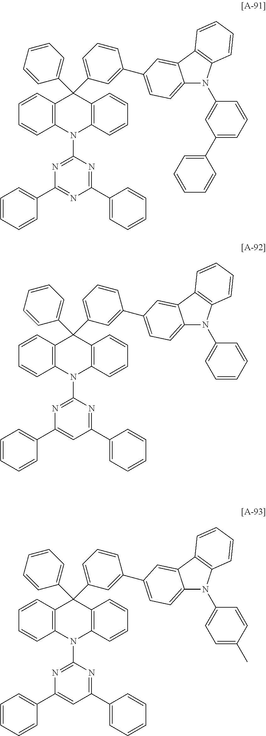


11. An organic light emitting diode, comprising:
an anode;
a cathode; and
at least one organic thin layer between the anode and cathode,
wherein the at least one organic thin layer includes the compound for an organic optoelectronic device as claimed in claim 1 .
12. The organic light emitting diode as claimed in claim 11 , wherein the at least one organic thin layer includes an emission layer, a hole transport layer (HTL), a hole injection layer (HIL), an electron transport layer (ETL), an electron injection layer (EIL), a hole blocking layer, or a combination thereof.
13. The organic light emitting diode as claimed in claim 11 , wherein:
the at least one organic thin layer includes an emission layer, and
the compound is included in the emission layer.
14. A display device comprising the organic light emitting diode as claimed in claim 11 .
Applications Claiming Priority (3)
| Application Number | Priority Date | Filing Date | Title |
|---|---|---|---|
| KR20120111344 | 2012-10-08 | ||
| KR10-2012-0111344 | 2012-10-08 | ||
| PCT/KR2013/004653 WO2014058123A1 (en) | 2012-10-08 | 2013-05-28 | Compound for organic optoelectric device, organic light emitting diode comprising same, and display device comprising organic light emitting diode |
Related Parent Applications (1)
| Application Number | Title | Priority Date | Filing Date |
|---|---|---|---|
| PCT/KR2013/004653 Continuation WO2014058123A1 (en) | 2012-10-08 | 2013-05-28 | Compound for organic optoelectric device, organic light emitting diode comprising same, and display device comprising organic light emitting diode |
Publications (2)
| Publication Number | Publication Date |
|---|---|
| US20150200372A1 US20150200372A1 (en) | 2015-07-16 |
| US9722186B2 true US9722186B2 (en) | 2017-08-01 |
Family
ID=50477567
Family Applications (1)
| Application Number | Title | Priority Date | Filing Date |
|---|---|---|---|
| US14/669,511 Active 2034-03-31 US9722186B2 (en) | 2012-10-08 | 2015-03-26 | Compound for organic optoelectronic device, organic light emitting diode comprising same, and display comprising organic light emitting diode |
Country Status (4)
| Country | Link |
|---|---|
| US (1) | US9722186B2 (en) |
| JP (1) | JP2016500669A (en) |
| KR (1) | KR101636848B1 (en) |
| WO (1) | WO2014058123A1 (en) |
Families Citing this family (13)
| Publication number | Priority date | Publication date | Assignee | Title |
|---|---|---|---|---|
| KR101636864B1 (en) * | 2012-10-08 | 2016-07-06 | 제일모직 주식회사 | Compound for organic optoelectronic device, organic light emitting diode including the same and display including the organic light emitting diode |
| KR101970979B1 (en) | 2014-04-16 | 2019-04-23 | 주식회사 만도 | Safety apparatus for Steer-By-Wire |
| CN107406391B (en) * | 2015-09-30 | 2021-02-19 | 株式会社Lg化学 | Spiro compound and organic light-emitting element comprising same |
| WO2017105041A1 (en) * | 2015-12-15 | 2017-06-22 | 주식회사 두산 | Organic compound and organic electroluminescent device comprising same |
| WO2017118209A1 (en) * | 2016-01-07 | 2017-07-13 | 广州华睿光电材料有限公司 | Silicon-containing organic compound and applications thereof |
| US9944627B2 (en) * | 2016-05-09 | 2018-04-17 | National Taiwan University | Spiroacridine-triazine hybrids and applications for electroluminescent devices |
| KR102610868B1 (en) * | 2016-06-02 | 2023-12-07 | 솔루스첨단소재 주식회사 | Organic compounds and organic electro luminescence device comprising the same |
| CN107586307B (en) * | 2016-07-08 | 2020-06-30 | 上海和辉光电有限公司 | Silafluorene derivative for electroluminescent material |
| TWI653231B (en) * | 2016-08-09 | 2019-03-11 | 南韓商Lg化學股份有限公司 | Compound and organic light emitting device comprising the same |
| KR102633650B1 (en) * | 2016-10-27 | 2024-02-06 | 솔루스첨단소재 주식회사 | Organic compounds and organic electro luminescence device comprising the same |
| WO2018216913A1 (en) * | 2017-05-22 | 2018-11-29 | 주식회사 엘지화학 | Novel heterocyclic compound and organic light-emitting device using same |
| WO2019004796A1 (en) * | 2017-06-30 | 2019-01-03 | 주식회사 엘지화학 | Novel heterocyclic compound and organic light-emitting device using same |
| KR102664158B1 (en) * | 2018-12-24 | 2024-05-08 | 엘지디스플레이 주식회사 | Organic compounds, organic light emitting diode and organic light emitting device haivng the compounds |
Citations (16)
| Publication number | Priority date | Publication date | Assignee | Title |
|---|---|---|---|---|
| US7014925B2 (en) | 2003-04-29 | 2006-03-21 | Canon Kabushiki Kaisha | Heterogeneous spiro compounds in organic light emitting device elements |
| KR20060051620A (en) | 2004-09-24 | 2006-05-19 | 주식회사 엘지화학 | New compound and organic light emitting device using the same(9) |
| WO2008123189A1 (en) | 2007-03-26 | 2008-10-16 | Nippon Steel Chemical Co., Ltd. | Compound for organic electroluminescent device and organic electroluminescent device |
| WO2009047147A1 (en) | 2007-10-02 | 2009-04-16 | Basf Se | Use of acridine derivatives as matrix materials and/or an electron blocker in oleds |
| US7838129B2 (en) * | 2004-09-24 | 2010-11-23 | Lg Chem, Ltd. | Compound and organic light emitting device using the same |
| JP2011501787A (en) | 2007-10-16 | 2011-01-13 | コーニンクレッカ フィリップス エレクトロニクス エヌ ヴィ | Multi-layered fabric display |
| KR20110049244A (en) | 2009-11-04 | 2011-05-12 | 다우어드밴스드디스플레이머티리얼 유한회사 | Novel organic electroluminescent compounds and organic electroluminescent device using the same |
| KR20110053114A (en) | 2009-11-13 | 2011-05-19 | 주식회사 엘지화학 | New fused cyclic compound and organic electronic device |
| KR20110102055A (en) | 2010-03-10 | 2011-09-16 | 제일모직주식회사 | Compound for organic photoelectric device and organic photoelectric device including the same |
| KR20110107682A (en) | 2010-03-25 | 2011-10-04 | 에스에프씨 주식회사 | Spiro compound and organic electroluminescent devices comprising the same |
| KR20110110508A (en) | 2010-04-01 | 2011-10-07 | 에스에프씨 주식회사 | Spiro compound and organic electroluminescent devices comprising the same |
| KR20110111093A (en) | 2010-04-02 | 2011-10-10 | 에스에프씨 주식회사 | Spiro compounds and organic light-emitting diode including the same |
| KR20120015883A (en) | 2010-08-13 | 2012-02-22 | 주식회사 엘지화학 | New compounds and organic electronic device using the same |
| KR101120892B1 (en) | 2009-06-19 | 2012-02-27 | 주식회사 두산 | Acridine derivative and organic electroluminescence device comprising the same |
| KR20120021215A (en) | 2010-08-31 | 2012-03-08 | 롬엔드하스전자재료코리아유한회사 | Novel organic electroluminescent compounds and organic electroluminescent device using the same |
| KR20120038032A (en) | 2010-10-07 | 2012-04-23 | 에스에프씨 주식회사 | Heterocyclic com pounds and organic light-emitting diode including the same |
-
2013
- 2013-05-28 WO PCT/KR2013/004653 patent/WO2014058123A1/en active Application Filing
- 2013-05-28 KR KR1020130060518A patent/KR101636848B1/en active IP Right Grant
- 2013-05-28 JP JP2015535554A patent/JP2016500669A/en active Pending
-
2015
- 2015-03-26 US US14/669,511 patent/US9722186B2/en active Active
Patent Citations (20)
| Publication number | Priority date | Publication date | Assignee | Title |
|---|---|---|---|---|
| US7014925B2 (en) | 2003-04-29 | 2006-03-21 | Canon Kabushiki Kaisha | Heterogeneous spiro compounds in organic light emitting device elements |
| KR20060051620A (en) | 2004-09-24 | 2006-05-19 | 주식회사 엘지화학 | New compound and organic light emitting device using the same(9) |
| KR100642995B1 (en) | 2004-09-24 | 2006-11-10 | 주식회사 엘지화학 | New compound and organic light emitting device using the same8 |
| US7838129B2 (en) * | 2004-09-24 | 2010-11-23 | Lg Chem, Ltd. | Compound and organic light emitting device using the same |
| JP4642849B2 (en) | 2004-09-24 | 2011-03-02 | エルジー・ケム・リミテッド | New organic light emitting device material and organic light emitting device using the same (1) |
| WO2008123189A1 (en) | 2007-03-26 | 2008-10-16 | Nippon Steel Chemical Co., Ltd. | Compound for organic electroluminescent device and organic electroluminescent device |
| WO2009047147A1 (en) | 2007-10-02 | 2009-04-16 | Basf Se | Use of acridine derivatives as matrix materials and/or an electron blocker in oleds |
| US20100219406A1 (en) | 2007-10-02 | 2010-09-02 | Basf Se | Use of acridine derivatives as matrix materials and/or electron blockers in oleds |
| JP2011501787A (en) | 2007-10-16 | 2011-01-13 | コーニンクレッカ フィリップス エレクトロニクス エヌ ヴィ | Multi-layered fabric display |
| KR101120892B1 (en) | 2009-06-19 | 2012-02-27 | 주식회사 두산 | Acridine derivative and organic electroluminescence device comprising the same |
| KR20110049244A (en) | 2009-11-04 | 2011-05-12 | 다우어드밴스드디스플레이머티리얼 유한회사 | Novel organic electroluminescent compounds and organic electroluminescent device using the same |
| KR20110053114A (en) | 2009-11-13 | 2011-05-19 | 주식회사 엘지화학 | New fused cyclic compound and organic electronic device |
| WO2011059271A2 (en) | 2009-11-13 | 2011-05-19 | 주식회사 엘지화학 | Novel compound having condensed ring, and organic electronic device using same |
| KR20110102055A (en) | 2010-03-10 | 2011-09-16 | 제일모직주식회사 | Compound for organic photoelectric device and organic photoelectric device including the same |
| KR20110107682A (en) | 2010-03-25 | 2011-10-04 | 에스에프씨 주식회사 | Spiro compound and organic electroluminescent devices comprising the same |
| KR20110110508A (en) | 2010-04-01 | 2011-10-07 | 에스에프씨 주식회사 | Spiro compound and organic electroluminescent devices comprising the same |
| KR20110111093A (en) | 2010-04-02 | 2011-10-10 | 에스에프씨 주식회사 | Spiro compounds and organic light-emitting diode including the same |
| KR20120015883A (en) | 2010-08-13 | 2012-02-22 | 주식회사 엘지화학 | New compounds and organic electronic device using the same |
| KR20120021215A (en) | 2010-08-31 | 2012-03-08 | 롬엔드하스전자재료코리아유한회사 | Novel organic electroluminescent compounds and organic electroluminescent device using the same |
| KR20120038032A (en) | 2010-10-07 | 2012-04-23 | 에스에프씨 주식회사 | Heterocyclic com pounds and organic light-emitting diode including the same |
Also Published As
| Publication number | Publication date |
|---|---|
| KR20140045266A (en) | 2014-04-16 |
| KR101636848B1 (en) | 2016-07-07 |
| US20150200372A1 (en) | 2015-07-16 |
| JP2016500669A (en) | 2016-01-14 |
| WO2014058123A1 (en) | 2014-04-17 |
Similar Documents
| Publication | Publication Date | Title |
|---|---|---|
| US9722186B2 (en) | Compound for organic optoelectronic device, organic light emitting diode comprising same, and display comprising organic light emitting diode | |
| US10121973B2 (en) | Compound for organic optoelectronic device, organic light-emitting diode including same, and display device including organic light-emitting diode | |
| US20150144937A1 (en) | Compound for organic optoelectronic device, organic light emitting diode comprising same, and display device comprising organic light emitting diode | |
| US10153436B2 (en) | Compound for an organic optoelectronic element, organic light-emitting element comprising same, and display device comprising the organic light-emitting element | |
| US9368733B2 (en) | Compound for organic optoelectronic device, organic light-emitting device containing the same, and display device including said organic light-emitting device | |
| US9324948B2 (en) | Compound for organic optoelectronic device, organic light emitting diode including the same and display including the organic light emitting diode | |
| US20150263294A1 (en) | Compound for organic optoelectronic device, organic light-emitting device including same, and display device including the organic light- emitting diode | |
| US9543530B2 (en) | Compound for organic optoelectronic device, organic light emitting diode including the same and display including the organic light emitting diode | |
| US9559309B2 (en) | Compound for organic optoelectronic device, organic light emitting diode including the same, and display device including the organic light emitting diode | |
| US9406891B2 (en) | Compound for organic optoelectronic device, organic light emitting diode including the same, and display including the organic light emitting diode | |
| US9502662B2 (en) | Compound for an organic optoelectronic device, organic light-emitting element comprising same, and display device comprising the organic light-emitting element | |
| US9793488B2 (en) | Compound for organic optoelectronic element, organic light-emitting element comprising same, and display device comprising the organic light-emitting element | |
| US11746093B2 (en) | Nitrogen-containing compound, electronic element, and electronic device | |
| US9444054B2 (en) | Compound for organic optoelectronic device and organic light emitting diode including the same | |
| KR20140087996A (en) | Compound for organic optoelectronic device, organic light emitting diode including the same and display including the organic light emitting diode | |
| US9419229B2 (en) | Compound, organic optoelectric device including the same and display device including the optoelectric device | |
| KR20130078749A (en) | Compound for organic optoelectronic device, organic light emitting diode including the same and display including the organic light emitting diode | |
| US10141521B2 (en) | Compound, organic optoelectronic element comprising same, and display device | |
| US20150021563A1 (en) | Compound for organic optoelectronic device, organic light emitting diode including the same and display including the organic light emitting diode | |
| US10096784B2 (en) | Compound for organic optoelectric device, composition for organic optoelectric device and organic optoelectric device and display device | |
| US9825242B2 (en) | Compound for organic optoelectric device, organic light-emitting diode including same, display device including organic light-emitting diode | |
| KR20140045154A (en) | Compound for organic optoelectronic device, organic light emitting diode including the same and display including the organic light emitting diode | |
| US9543528B2 (en) | Compound for an organic optoelectric device, organic optoelectric device including the same, and display device including the optoelectric device | |
| US11056655B2 (en) | Organic compound for optoelectric device and organic optoelectric device and display device |
Legal Events
| Date | Code | Title | Description |
|---|---|---|---|
| AS | Assignment |
Owner name: SAMSUNG SDI CO., LTD., KOREA, REPUBLIC OF Free format text: ASSIGNMENT OF ASSIGNORS INTEREST;ASSIGNORS:PARK, MOO-JIN;YU, EUN-SUN;CHAE, MI-YOUNG;AND OTHERS;REEL/FRAME:035264/0167 Effective date: 20150309 |
|
| STCF | Information on status: patent grant |
Free format text: PATENTED CASE |
|
| MAFP | Maintenance fee payment |
Free format text: PAYMENT OF MAINTENANCE FEE, 4TH YEAR, LARGE ENTITY (ORIGINAL EVENT CODE: M1551); ENTITY STATUS OF PATENT OWNER: LARGE ENTITY Year of fee payment: 4 |