US20130292659A1 - Compound for organic optoelectronic device, organic light emitting diode including the same, and display device including the organic light emitting diode - Google Patents
Compound for organic optoelectronic device, organic light emitting diode including the same, and display device including the organic light emitting diode Download PDFInfo
- Publication number
- US20130292659A1 US20130292659A1 US13/914,008 US201313914008A US2013292659A1 US 20130292659 A1 US20130292659 A1 US 20130292659A1 US 201313914008 A US201313914008 A US 201313914008A US 2013292659 A1 US2013292659 A1 US 2013292659A1
- Authority
- US
- United States
- Prior art keywords
- substituted
- unsubstituted
- group
- compound
- light emitting
- Prior art date
- Legal status (The legal status is an assumption and is not a legal conclusion. Google has not performed a legal analysis and makes no representation as to the accuracy of the status listed.)
- Granted
Links
- 150000001875 compounds Chemical class 0.000 title claims abstract description 109
- 230000005693 optoelectronics Effects 0.000 title claims abstract description 68
- 239000000126 substance Substances 0.000 claims abstract description 50
- 125000003118 aryl group Chemical group 0.000 claims description 42
- 125000001072 heteroaryl group Chemical group 0.000 claims description 39
- 238000002347 injection Methods 0.000 claims description 28
- 239000007924 injection Substances 0.000 claims description 28
- YZCKVEUIGOORGS-OUBTZVSYSA-N Deuterium Chemical group [2H] YZCKVEUIGOORGS-OUBTZVSYSA-N 0.000 claims description 18
- 229910052805 deuterium Inorganic materials 0.000 claims description 18
- 229910052739 hydrogen Inorganic materials 0.000 claims description 18
- 239000001257 hydrogen Substances 0.000 claims description 18
- UFHFLCQGNIYNRP-UHFFFAOYSA-N Hydrogen Chemical compound [H][H] UFHFLCQGNIYNRP-UHFFFAOYSA-N 0.000 claims description 17
- 230000005525 hole transport Effects 0.000 claims description 17
- 230000000903 blocking effect Effects 0.000 claims description 5
- -1 oxatriazolyl group Chemical group 0.000 claims description 4
- YJTKZCDBKVTVBY-UHFFFAOYSA-N 1,3-Diphenylbenzene Chemical group C1=CC=CC=C1C1=CC=CC(C=2C=CC=CC=2)=C1 YJTKZCDBKVTVBY-UHFFFAOYSA-N 0.000 claims description 2
- 125000000641 acridinyl group Chemical group C1(=CC=CC2=NC3=CC=CC=C3C=C12)* 0.000 claims description 2
- 125000003785 benzimidazolyl group Chemical group N1=C(NC2=C1C=CC=C2)* 0.000 claims description 2
- 125000003354 benzotriazolyl group Chemical group N1N=NC2=C1C=CC=C2* 0.000 claims description 2
- 125000003983 fluorenyl group Chemical group C1(=CC=CC=2C3=CC=CC=C3CC12)* 0.000 claims description 2
- 125000002883 imidazolyl group Chemical group 0.000 claims description 2
- 125000002183 isoquinolinyl group Chemical group C1(=NC=CC2=CC=CC=C12)* 0.000 claims description 2
- 125000001715 oxadiazolyl group Chemical group 0.000 claims description 2
- 125000002080 perylenyl group Chemical group C1(=CC=C2C=CC=C3C4=CC=CC5=CC=CC(C1=C23)=C45)* 0.000 claims description 2
- 125000001792 phenanthrenyl group Chemical group C1(=CC=CC=2C3=CC=CC=C3C=CC12)* 0.000 claims description 2
- 125000004625 phenanthrolinyl group Chemical group N1=C(C=CC2=CC=C3C=CC=NC3=C12)* 0.000 claims description 2
- 125000001791 phenazinyl group Chemical group C1(=CC=CC2=NC3=CC=CC=C3N=C12)* 0.000 claims description 2
- 125000004592 phthalazinyl group Chemical group C1(=NN=CC2=CC=CC=C12)* 0.000 claims description 2
- 125000000561 purinyl group Chemical group N1=C(N=C2N=CNC2=C1)* 0.000 claims description 2
- 125000003373 pyrazinyl group Chemical group 0.000 claims description 2
- 125000001725 pyrenyl group Chemical group 0.000 claims description 2
- 125000002098 pyridazinyl group Chemical group 0.000 claims description 2
- 125000004076 pyridyl group Chemical group 0.000 claims description 2
- 125000000714 pyrimidinyl group Chemical group 0.000 claims description 2
- 125000002294 quinazolinyl group Chemical group N1=C(N=CC2=CC=CC=C12)* 0.000 claims description 2
- 125000002943 quinolinyl group Chemical group N1=C(C=CC2=CC=CC=C12)* 0.000 claims description 2
- 125000001567 quinoxalinyl group Chemical group N1=C(C=NC2=CC=CC=C12)* 0.000 claims description 2
- 125000003831 tetrazolyl group Chemical group 0.000 claims description 2
- 125000005307 thiatriazolyl group Chemical group S1N=NN=C1* 0.000 claims description 2
- 125000004306 triazinyl group Chemical group 0.000 claims description 2
- 125000001425 triazolyl group Chemical group 0.000 claims description 2
- 125000004435 hydrogen atom Chemical group [H]* 0.000 claims 1
- 238000004519 manufacturing process Methods 0.000 abstract description 9
- 239000010410 layer Substances 0.000 description 106
- 239000000463 material Substances 0.000 description 42
- UJOBWOGCFQCDNV-UHFFFAOYSA-N 9H-carbazole Chemical compound C1=CC=C2C3=CC=CC=C3NC2=C1 UJOBWOGCFQCDNV-UHFFFAOYSA-N 0.000 description 29
- ZMXDDKWLCZADIW-UHFFFAOYSA-N N,N-Dimethylformamide Chemical compound CN(C)C=O ZMXDDKWLCZADIW-UHFFFAOYSA-N 0.000 description 21
- 125000001424 substituent group Chemical group 0.000 description 21
- OKKJLVBELUTLKV-UHFFFAOYSA-N Methanol Chemical compound OC OKKJLVBELUTLKV-UHFFFAOYSA-N 0.000 description 18
- YXFVVABEGXRONW-UHFFFAOYSA-N Toluene Chemical compound CC1=CC=CC=C1 YXFVVABEGXRONW-UHFFFAOYSA-N 0.000 description 18
- 0 CC=C(*=C(c(cc1)ccc1-c1ccccc1)N=C(C)c1ccccc1)c(cc1)ccc1-[n](c(ccc(-[n]1c2ccccc2c2c1cccc2)c1)c1c1c2)c1ccc2-[n]1c2ccccc2c2ccccc12 Chemical compound CC=C(*=C(c(cc1)ccc1-c1ccccc1)N=C(C)c1ccccc1)c(cc1)ccc1-[n](c(ccc(-[n]1c2ccccc2c2c1cccc2)c1)c1c1c2)c1ccc2-[n]1c2ccccc2c2ccccc12 0.000 description 14
- MVPPADPHJFYWMZ-UHFFFAOYSA-N chlorobenzene Chemical compound ClC1=CC=CC=C1 MVPPADPHJFYWMZ-UHFFFAOYSA-N 0.000 description 14
- 239000007787 solid Substances 0.000 description 14
- VLKZOEOYAKHREP-UHFFFAOYSA-N n-Hexane Chemical compound CCCCCC VLKZOEOYAKHREP-UHFFFAOYSA-N 0.000 description 12
- 230000015572 biosynthetic process Effects 0.000 description 11
- 230000000052 comparative effect Effects 0.000 description 11
- 239000002019 doping agent Substances 0.000 description 11
- 238000003786 synthesis reaction Methods 0.000 description 11
- IJGRMHOSHXDMSA-UHFFFAOYSA-N Atomic nitrogen Chemical compound N#N IJGRMHOSHXDMSA-UHFFFAOYSA-N 0.000 description 10
- 239000011368 organic material Substances 0.000 description 10
- 125000000217 alkyl group Chemical group 0.000 description 9
- 238000006243 chemical reaction Methods 0.000 description 7
- WYURNTSHIVDZCO-UHFFFAOYSA-N Tetrahydrofuran Chemical compound C1CCOC1 WYURNTSHIVDZCO-UHFFFAOYSA-N 0.000 description 6
- 230000007423 decrease Effects 0.000 description 6
- 238000000034 method Methods 0.000 description 6
- BWHMMNNQKKPAPP-UHFFFAOYSA-L potassium carbonate Chemical compound [K+].[K+].[O-]C([O-])=O BWHMMNNQKKPAPP-UHFFFAOYSA-L 0.000 description 6
- XLYOFNOQVPJJNP-UHFFFAOYSA-N water Substances O XLYOFNOQVPJJNP-UHFFFAOYSA-N 0.000 description 6
- 230000008901 benefit Effects 0.000 description 5
- 239000011203 carbon fibre reinforced carbon Substances 0.000 description 5
- 125000005842 heteroatom Chemical group 0.000 description 5
- 238000005259 measurement Methods 0.000 description 5
- 239000000243 solution Substances 0.000 description 5
- 239000002904 solvent Substances 0.000 description 5
- VQGHOUODWALEFC-UHFFFAOYSA-N 2-phenylpyridine Chemical compound C1=CC=CC=C1C1=CC=CC=N1 VQGHOUODWALEFC-UHFFFAOYSA-N 0.000 description 4
- FIHILUSWISKVSR-UHFFFAOYSA-N 3,6-dibromo-9h-carbazole Chemical compound C1=C(Br)C=C2C3=CC(Br)=CC=C3NC2=C1 FIHILUSWISKVSR-UHFFFAOYSA-N 0.000 description 4
- XLOMVQKBTHCTTD-UHFFFAOYSA-N Zinc monoxide Chemical compound [Zn]=O XLOMVQKBTHCTTD-UHFFFAOYSA-N 0.000 description 4
- 125000000609 carbazolyl group Chemical group C1(=CC=CC=2C3=CC=CC=C3NC12)* 0.000 description 4
- 230000008859 change Effects 0.000 description 4
- 239000003610 charcoal Substances 0.000 description 4
- 230000021615 conjugation Effects 0.000 description 4
- 229910052751 metal Inorganic materials 0.000 description 4
- 239000002184 metal Substances 0.000 description 4
- 239000000203 mixture Substances 0.000 description 4
- 229910052757 nitrogen Inorganic materials 0.000 description 4
- 229910000104 sodium hydride Inorganic materials 0.000 description 4
- MFRIHAYPQRLWNB-UHFFFAOYSA-N sodium tert-butoxide Chemical compound [Na+].CC(C)(C)[O-] MFRIHAYPQRLWNB-UHFFFAOYSA-N 0.000 description 4
- BWHDROKFUHTORW-UHFFFAOYSA-N tritert-butylphosphane Chemical compound CC(C)(C)P(C(C)(C)C)C(C)(C)C BWHDROKFUHTORW-UHFFFAOYSA-N 0.000 description 4
- KFZMGEQAYNKOFK-UHFFFAOYSA-N Isopropanol Chemical compound CC(C)O KFZMGEQAYNKOFK-UHFFFAOYSA-N 0.000 description 3
- 125000002009 alkene group Chemical group 0.000 description 3
- 125000004450 alkenylene group Chemical group 0.000 description 3
- 125000002355 alkine group Chemical group 0.000 description 3
- 125000004419 alkynylene group Chemical group 0.000 description 3
- 229910052782 aluminium Inorganic materials 0.000 description 3
- XAGFODPZIPBFFR-UHFFFAOYSA-N aluminium Chemical compound [Al] XAGFODPZIPBFFR-UHFFFAOYSA-N 0.000 description 3
- 239000007864 aqueous solution Substances 0.000 description 3
- 125000000732 arylene group Chemical group 0.000 description 3
- 239000011575 calcium Substances 0.000 description 3
- 238000000576 coating method Methods 0.000 description 3
- 239000003086 colorant Substances 0.000 description 3
- 238000000151 deposition Methods 0.000 description 3
- 229910001873 dinitrogen Inorganic materials 0.000 description 3
- 230000005283 ground state Effects 0.000 description 3
- 238000010438 heat treatment Methods 0.000 description 3
- 125000005549 heteroarylene group Chemical group 0.000 description 3
- NFHFRUOZVGFOOS-UHFFFAOYSA-N palladium;triphenylphosphane Chemical compound [Pd].C1=CC=CC=C1P(C=1C=CC=CC=1)C1=CC=CC=C1.C1=CC=CC=C1P(C=1C=CC=CC=1)C1=CC=CC=C1.C1=CC=CC=C1P(C=1C=CC=CC=1)C1=CC=CC=C1.C1=CC=CC=C1P(C=1C=CC=CC=1)C1=CC=CC=C1 NFHFRUOZVGFOOS-UHFFFAOYSA-N 0.000 description 3
- 229910000027 potassium carbonate Inorganic materials 0.000 description 3
- 239000000376 reactant Substances 0.000 description 3
- 230000027756 respiratory electron transport chain Effects 0.000 description 3
- 238000007711 solidification Methods 0.000 description 3
- 230000008023 solidification Effects 0.000 description 3
- 239000000758 substrate Substances 0.000 description 3
- YLQBMQCUIZJEEH-UHFFFAOYSA-N tetrahydrofuran Natural products C=1C=COC=1 YLQBMQCUIZJEEH-UHFFFAOYSA-N 0.000 description 3
- ZSYMVHGRKPBJCQ-UHFFFAOYSA-N 1,1'-biphenyl;9h-carbazole Chemical group C1=CC=CC=C1C1=CC=CC=C1.C1=CC=C2C3=CC=CC=C3NC2=C1 ZSYMVHGRKPBJCQ-UHFFFAOYSA-N 0.000 description 2
- WTAPZWXVSZMMDG-UHFFFAOYSA-N 1,5-diphenylpenta-1,4-dien-3-one;palladium Chemical compound [Pd].C=1C=CC=CC=1C=CC(=O)C=CC1=CC=CC=C1 WTAPZWXVSZMMDG-UHFFFAOYSA-N 0.000 description 2
- QPTWWBLGJZWRAV-UHFFFAOYSA-N 2,7-dibromo-9-H-carbazole Natural products BrC1=CC=C2C3=CC=C(Br)C=C3NC2=C1 QPTWWBLGJZWRAV-UHFFFAOYSA-N 0.000 description 2
- AWXGSYPUMWKTBR-UHFFFAOYSA-N 4-carbazol-9-yl-n,n-bis(4-carbazol-9-ylphenyl)aniline Chemical compound C12=CC=CC=C2C2=CC=CC=C2N1C1=CC=C(N(C=2C=CC(=CC=2)N2C3=CC=CC=C3C3=CC=CC=C32)C=2C=CC(=CC=2)N2C3=CC=CC=C3C3=CC=CC=C32)C=C1 AWXGSYPUMWKTBR-UHFFFAOYSA-N 0.000 description 2
- CSCPPACGZOOCGX-UHFFFAOYSA-N Acetone Chemical compound CC(C)=O CSCPPACGZOOCGX-UHFFFAOYSA-N 0.000 description 2
- CFRIIAAUARATGS-UHFFFAOYSA-N C1=CC2=C(C=C1)C(C1=CC(C3=CC=CC4=C3C=CC=C4)=NC(C3=CC=C(N4C5=C(C=C(N6C7=C(C=CC=C7)C7=C6C=CC=C7)C=C5)C5=C4C=CC(N4C6=C(C=CC=C6)C6=C4C=CC=C6)=C5)C=C3)=N1)=CC=C2.C1=CC2=C(C=C1)N(C1=CC3=C(C=C1)N(C1=CC=C(C4=NC(N5C6=C(C=CC=C6)C6=C5C=CC=C6)=CC(N5C6=C(C=CC=C6)C6=C5C=CC=C6)=N4)C=C1)C1=C3C=C(N3C4=C(C=CC=C4)C4=C3C=CC=C4)C=C1)C1=C2C=CC=C1 Chemical compound C1=CC2=C(C=C1)C(C1=CC(C3=CC=CC4=C3C=CC=C4)=NC(C3=CC=C(N4C5=C(C=C(N6C7=C(C=CC=C7)C7=C6C=CC=C7)C=C5)C5=C4C=CC(N4C6=C(C=CC=C6)C6=C4C=CC=C6)=C5)C=C3)=N1)=CC=C2.C1=CC2=C(C=C1)N(C1=CC3=C(C=C1)N(C1=CC=C(C4=NC(N5C6=C(C=CC=C6)C6=C5C=CC=C6)=CC(N5C6=C(C=CC=C6)C6=C5C=CC=C6)=N4)C=C1)C1=C3C=C(N3C4=C(C=CC=C4)C4=C3C=CC=C4)C=C1)C1=C2C=CC=C1 CFRIIAAUARATGS-UHFFFAOYSA-N 0.000 description 2
- VMAMBOUXNLBUPU-UHFFFAOYSA-N C1=CC2=C(C=C1)C(C1=CC(C3=CC=CC4=C3C=CC=C4)=NC(N3C4=C(C=C(N5C6=C(C=CC=C6)C6=C5C=CC=C6)C=C4)C4=C3C=CC(N3C5=C(C=CC=C5)C5=C3C=CC=C5)=C4)=N1)=CC=C2.C1=CC2=C(C=C1)N(C1=CC3=C(C=C1)N(C1=NC(N4C5=C(C=CC=C5)C5=C4C=CC=C5)=CC(N4C5=C(C=CC=C5)C5=C4C=CC=C5)=N1)C1=C3C=C(N3C4=C(C=CC=C4)C4=C3C=CC=C4)C=C1)C1=C2C=CC=C1.C1=CC=C(C2=CC=C(C3=NC(N4C5=C(C=C(N6C7=C(C=CC=C7)C7=C6C=CC=C7)C=C5)C5=C4C=CC(N4C6=C(C=CC=C6)C6=C4C=CC=C6)=C5)=NC(C4=CC=CC=C4)=C3)C=C2)C=C1 Chemical compound C1=CC2=C(C=C1)C(C1=CC(C3=CC=CC4=C3C=CC=C4)=NC(N3C4=C(C=C(N5C6=C(C=CC=C6)C6=C5C=CC=C6)C=C4)C4=C3C=CC(N3C5=C(C=CC=C5)C5=C3C=CC=C5)=C4)=N1)=CC=C2.C1=CC2=C(C=C1)N(C1=CC3=C(C=C1)N(C1=NC(N4C5=C(C=CC=C5)C5=C4C=CC=C5)=CC(N4C5=C(C=CC=C5)C5=C4C=CC=C5)=N1)C1=C3C=C(N3C4=C(C=CC=C4)C4=C3C=CC=C4)C=C1)C1=C2C=CC=C1.C1=CC=C(C2=CC=C(C3=NC(N4C5=C(C=C(N6C7=C(C=CC=C7)C7=C6C=CC=C7)C=C5)C5=C4C=CC(N4C6=C(C=CC=C6)C6=C4C=CC=C6)=C5)=NC(C4=CC=CC=C4)=C3)C=C2)C=C1 VMAMBOUXNLBUPU-UHFFFAOYSA-N 0.000 description 2
- HBNIIBOGHOKMCM-UHFFFAOYSA-N C1=CC2=C(C=C1)C(C1=NC(C3=CC=C(N4C5=C(C=C(N6C7=C(C=CC=C7)C7=C6C=CC=C7)C=C5)C5=C4C=CC(N4C6=C(C=CC=C6)C6=C4C=CC=C6)=C5)C=C3)=NC(C3=CC=CC4=C3C=CC=C4)=N1)=CC=C2.C1=CC=C(C2=CC=C(C3=NC(C4=CC=C(N5C6=C(C=C(N7C8=C(C=CC=C8)C8=C7C=CC=C8)C=C6)C6=C5C=CC(N5C7=C(C=CC=C7)C7=C5C=CC=C7)=C6)C=C4)=NC(C4=CC=CC=C4)=N3)C=C2)C=C1 Chemical compound C1=CC2=C(C=C1)C(C1=NC(C3=CC=C(N4C5=C(C=C(N6C7=C(C=CC=C7)C7=C6C=CC=C7)C=C5)C5=C4C=CC(N4C6=C(C=CC=C6)C6=C4C=CC=C6)=C5)C=C3)=NC(C3=CC=CC4=C3C=CC=C4)=N1)=CC=C2.C1=CC=C(C2=CC=C(C3=NC(C4=CC=C(N5C6=C(C=C(N7C8=C(C=CC=C8)C8=C7C=CC=C8)C=C6)C6=C5C=CC(N5C7=C(C=CC=C7)C7=C5C=CC=C7)=C6)C=C4)=NC(C4=CC=CC=C4)=N3)C=C2)C=C1 HBNIIBOGHOKMCM-UHFFFAOYSA-N 0.000 description 2
- JGFLHSXZSFMLHG-UHFFFAOYSA-N C1=CC2=C(C=C1)C(C1=NC(C3=CC=CC4=C3C=CC=C4)=NC(N3C4=C(C=C(N5C6=C(C=CC=C6)C6=C5C=CC=C6)C=C4)C4=C3C=CC(N3C5=C(C=CC=C5)C5=C3C=CC=C5)=C4)=N1)=CC=C2.C1=CC2=C(C=C1)N(C1=CC3=C(C=C1)N(C1=NC(N4C5=C(C=CC=C5)C5=C4C=CC=C5)=NC(N4C5=C(C=CC=C5)C5=C4C=CC=C5)=N1)C1=C3C=C(N3C4=C(C=CC=C4)C4=C3C=CC=C4)C=C1)C1=C2C=CC=C1.C1=CC=C(C2=CC=C(C3=NC(N4C5=C(C=C(N6C7=C(C=CC=C7)C7=C6C=CC=C7)C=C5)C5=C4C=CC(N4C6=C(C=CC=C6)C6=C4C=CC=C6)=C5)=NC(C4=CC=CC=C4)=N3)C=C2)C=C1 Chemical compound C1=CC2=C(C=C1)C(C1=NC(C3=CC=CC4=C3C=CC=C4)=NC(N3C4=C(C=C(N5C6=C(C=CC=C6)C6=C5C=CC=C6)C=C4)C4=C3C=CC(N3C5=C(C=CC=C5)C5=C3C=CC=C5)=C4)=N1)=CC=C2.C1=CC2=C(C=C1)N(C1=CC3=C(C=C1)N(C1=NC(N4C5=C(C=CC=C5)C5=C4C=CC=C5)=NC(N4C5=C(C=CC=C5)C5=C4C=CC=C5)=N1)C1=C3C=C(N3C4=C(C=CC=C4)C4=C3C=CC=C4)C=C1)C1=C2C=CC=C1.C1=CC=C(C2=CC=C(C3=NC(N4C5=C(C=C(N6C7=C(C=CC=C7)C7=C6C=CC=C7)C=C5)C5=C4C=CC(N4C6=C(C=CC=C6)C6=C4C=CC=C6)=C5)=NC(C4=CC=CC=C4)=N3)C=C2)C=C1 JGFLHSXZSFMLHG-UHFFFAOYSA-N 0.000 description 2
- VAMQOCRCGGLMKB-UHFFFAOYSA-N C1=CC2=C(C=C1)N(C1=CC3=C(C=C1)N(C1=C4C=CC=NC4=C4/N=C\C=C/C4=C1)C1=C3C=C(N3C4=C(C=CC=C4)C4=C3C=CC=C4)C=C1)C1=C2C=CC=C1.C1=CC2=CC=NC(N3C4=C(C=C(N5C6=C(C=CC=C6)C6=C5C=CC=C6)C=C4)C4=C3C=CC(N3C5=C(C=CC=C5)C5=C3C=CC=C5)=C4)=C2C=C1.C1=CC=C(C2=NN=C(C3=CC=C(N4C5=C(C=C(N6C7=C(C=CC=C7)C7=C6C=CC=C7)C=C5)C5=C4C=CC(N4C6=C(C=CC=C6)C6=C4C=CC=C6)=C5)C=C3)O2)C=C1 Chemical compound C1=CC2=C(C=C1)N(C1=CC3=C(C=C1)N(C1=C4C=CC=NC4=C4/N=C\C=C/C4=C1)C1=C3C=C(N3C4=C(C=CC=C4)C4=C3C=CC=C4)C=C1)C1=C2C=CC=C1.C1=CC2=CC=NC(N3C4=C(C=C(N5C6=C(C=CC=C6)C6=C5C=CC=C6)C=C4)C4=C3C=CC(N3C5=C(C=CC=C5)C5=C3C=CC=C5)=C4)=C2C=C1.C1=CC=C(C2=NN=C(C3=CC=C(N4C5=C(C=C(N6C7=C(C=CC=C7)C7=C6C=CC=C7)C=C5)C5=C4C=CC(N4C6=C(C=CC=C6)C6=C4C=CC=C6)=C5)C=C3)O2)C=C1 VAMQOCRCGGLMKB-UHFFFAOYSA-N 0.000 description 2
- AKTILPNYRKQJDN-UHFFFAOYSA-N C1=CC2=C(C=C1)N(C1=CC3=C(C=C1)N(C1=CC=C(C4=CC=NC=C4)C=C1)C1=C3C=C(N3C4=C(C=CC=C4)C4=C3C=CC=C4)C=C1)C1=C2C=CC=C1.C1=CC2=C(C=C1)N(C1=CC3=C(C=C1)N(C1=CC=NC=C1)C1=C3C=C(N3C4=C(C=CC=C4)C4=C3C=CC=C4)C=C1)C1=C2C=CC=C1.C1=CC=C(C2=CC(N3C4=C(C=C(N5C6=C(C=CC=C6)C6=C5C=CC=C6)C=C4)C4=C3C=CC(N3C5=C(C=CC=C5)C5=C3C=CC=C5)=C4)=CC(C3=CC=CC=C3)=N2)C=C1 Chemical compound C1=CC2=C(C=C1)N(C1=CC3=C(C=C1)N(C1=CC=C(C4=CC=NC=C4)C=C1)C1=C3C=C(N3C4=C(C=CC=C4)C4=C3C=CC=C4)C=C1)C1=C2C=CC=C1.C1=CC2=C(C=C1)N(C1=CC3=C(C=C1)N(C1=CC=NC=C1)C1=C3C=C(N3C4=C(C=CC=C4)C4=C3C=CC=C4)C=C1)C1=C2C=CC=C1.C1=CC=C(C2=CC(N3C4=C(C=C(N5C6=C(C=CC=C6)C6=C5C=CC=C6)C=C4)C4=C3C=CC(N3C5=C(C=CC=C5)C5=C3C=CC=C5)=C4)=CC(C3=CC=CC=C3)=N2)C=C1 AKTILPNYRKQJDN-UHFFFAOYSA-N 0.000 description 2
- TUCUZWBKSYOYHT-UHFFFAOYSA-N C1=CC2=C(C=C1)N(C1=CC3=C(C=C1)N(C1=CC=C(C4=NC(N5C6=C(C=CC=C6)C6=C5C=CC=C6)=NC(N5C6=C(C=CC=C6)C6=C5C=CC=C6)=N4)C=C1)C1=C3C=C(N3C4=C(C=CC=C4)C4=C3C=CC=C4)C=C1)C1=C2C=CC=C1.C1=CC=C(C2=CC=C(C3=NC(C4=CC=C(N5C6=C(C=C(N7C8=C(C=CC=C8)C8=C7C=CC=C8)C=C6)C6=C5C=CC(N5C7=C(C=CC=C7)C7=C5C=CC=C7)=C6)C=C4)=NC(C4=CC=CC=C4)=C3)C=C2)C=C1 Chemical compound C1=CC2=C(C=C1)N(C1=CC3=C(C=C1)N(C1=CC=C(C4=NC(N5C6=C(C=CC=C6)C6=C5C=CC=C6)=NC(N5C6=C(C=CC=C6)C6=C5C=CC=C6)=N4)C=C1)C1=C3C=C(N3C4=C(C=CC=C4)C4=C3C=CC=C4)C=C1)C1=C2C=CC=C1.C1=CC=C(C2=CC=C(C3=NC(C4=CC=C(N5C6=C(C=C(N7C8=C(C=CC=C8)C8=C7C=CC=C8)C=C6)C6=C5C=CC(N5C7=C(C=CC=C7)C7=C5C=CC=C7)=C6)C=C4)=NC(C4=CC=CC=C4)=C3)C=C2)C=C1 TUCUZWBKSYOYHT-UHFFFAOYSA-N 0.000 description 2
- QMCGURXHEHXUQH-UHFFFAOYSA-N C1=CC2=C(C=C1)N(C1=CC3=C(C=C1)N(C1=CN=CC=N1)C1=C3C=C(N3C4=C(C=CC=C4)C4=C3C=CC=C4)C=C1)C1=C2C=CC=C1.C1=CC2=C(C=C1)N=C(N1C3=C(C=C(N4C5=C(C=CC=C5)C5=C4C=CC=C5)C=C3)C3=C1C=CC(N1C4=C(C=CC=C4)C4=C1C=CC=C4)=C3)C=C2.C1=CC=C(C2=NN=C(C3=CC=CC=C3)N2C2=CC=C(N3C4=C(C=C(N5C6=C(C=CC=C6)C6=C5C=CC=C6)C=C4)C4=C3C=CC(N3C5=C(C=CC=C5)C5=C3C=CC=C5)=C4)C=C2)C=C1 Chemical compound C1=CC2=C(C=C1)N(C1=CC3=C(C=C1)N(C1=CN=CC=N1)C1=C3C=C(N3C4=C(C=CC=C4)C4=C3C=CC=C4)C=C1)C1=C2C=CC=C1.C1=CC2=C(C=C1)N=C(N1C3=C(C=C(N4C5=C(C=CC=C5)C5=C4C=CC=C5)C=C3)C3=C1C=CC(N1C4=C(C=CC=C4)C4=C1C=CC=C4)=C3)C=C2.C1=CC=C(C2=NN=C(C3=CC=CC=C3)N2C2=CC=C(N3C4=C(C=C(N5C6=C(C=CC=C6)C6=C5C=CC=C6)C=C4)C4=C3C=CC(N3C5=C(C=CC=C5)C5=C3C=CC=C5)=C4)C=C2)C=C1 QMCGURXHEHXUQH-UHFFFAOYSA-N 0.000 description 2
- SPTWUGRYZJWMQW-UHFFFAOYSA-N C1=CC2=C(C=C1)N=C(N1C3=C(C=C(N4C5=C(C=CC=C5)C5=C4C=CC=C5)C=C3)C3=C1C=CC(N1C4=C(C=CC=C4)C4=C1C=CC=C4)=C3)C=N2.C1=CC=C(C2=NC(N3C4=C(C=C(N5C6=C(C=CC=C6)C6=C5C=CC=C6)C=C4)C4=C3C=CC(N3C5=C(C=CC=C5)C5=C3C=CC=C5)=C4)=C3C=CC=CC3=N2)C=C1.C1=CC=C(N2C(C3=CC=C(N4C5=C(C=C(N6C7=C(C=CC=C7)C7=C6C=CC=C7)C=C5)C5=C4C=CC(N4C6=C(C=CC=C6)C6=C4C=CC=C6)=C5)C=C3)=NC3=C2C=CC=C3)C=C1 Chemical compound C1=CC2=C(C=C1)N=C(N1C3=C(C=C(N4C5=C(C=CC=C5)C5=C4C=CC=C5)C=C3)C3=C1C=CC(N1C4=C(C=CC=C4)C4=C1C=CC=C4)=C3)C=N2.C1=CC=C(C2=NC(N3C4=C(C=C(N5C6=C(C=CC=C6)C6=C5C=CC=C6)C=C4)C4=C3C=CC(N3C5=C(C=CC=C5)C5=C3C=CC=C5)=C4)=C3C=CC=CC3=N2)C=C1.C1=CC=C(N2C(C3=CC=C(N4C5=C(C=C(N6C7=C(C=CC=C7)C7=C6C=CC=C7)C=C5)C5=C4C=CC(N4C6=C(C=CC=C6)C6=C4C=CC=C6)=C5)C=C3)=NC3=C2C=CC=C3)C=C1 SPTWUGRYZJWMQW-UHFFFAOYSA-N 0.000 description 2
- CRYACEFVXAJBOB-UHFFFAOYSA-N C1=CC=C(C2=CC(C3=CC=C(N4C5=C(C=C(N6C7=C(C=CC=C7)C7=C6C=CC=C7)C=C5)C5=C4C=CC(N4C6=C(C=CC=C6)C6=C4C=CC=C6)=C5)C=C3)=CC(C3=CC=CC=C3)=N2)C=C1.C1=CC=C(C2=NC(C3=CC=CC=C3)=NC(C3=CC=C(N4C5=C(C=C(N6C7=C(C=CC=C7)C7=C6C=CC=C7)C=C5)C5=C4C=CC(N4C6=C(C=CC=C6)C6=C4C=CC=C6)=C5)C=C3)=C2)C=C1.C1=CC=C(C2=NC(C3=CC=CC=C3)=NC(N3C4=C(C=C(N5C6=C(C=CC=C6)C6=C5C=CC=C6)C=C4)C4=C3C=CC(N3C5=C(C=CC=C5)C5=C3C=CC=C5)=C4)=C2)C=C1 Chemical compound C1=CC=C(C2=CC(C3=CC=C(N4C5=C(C=C(N6C7=C(C=CC=C7)C7=C6C=CC=C7)C=C5)C5=C4C=CC(N4C6=C(C=CC=C6)C6=C4C=CC=C6)=C5)C=C3)=CC(C3=CC=CC=C3)=N2)C=C1.C1=CC=C(C2=NC(C3=CC=CC=C3)=NC(C3=CC=C(N4C5=C(C=C(N6C7=C(C=CC=C7)C7=C6C=CC=C7)C=C5)C5=C4C=CC(N4C6=C(C=CC=C6)C6=C4C=CC=C6)=C5)C=C3)=C2)C=C1.C1=CC=C(C2=NC(C3=CC=CC=C3)=NC(N3C4=C(C=C(N5C6=C(C=CC=C6)C6=C5C=CC=C6)C=C4)C4=C3C=CC(N3C5=C(C=CC=C5)C5=C3C=CC=C5)=C4)=C2)C=C1 CRYACEFVXAJBOB-UHFFFAOYSA-N 0.000 description 2
- VCVLGAHTPUNOFZ-UHFFFAOYSA-N C1=CC=C(C2=CC(C3=CC=CC=C3)=NC(C3=CC=C(N4C5=C(C=C(N6C7=C(C=CC=C7)C7=C6C=CC=C7)C=C5)C5=C4C=CC(N4C6=C(C=CC=C6)C6=C4C=CC=C6)=C5)C=C3)=C2)C=C1.C1=CC=C(C2=CC(C3=CC=CC=C3)=NC(C3=CC=C(N4C5=C(C=C(N6C7=C(C=CC=C7)C7=C6C=CC=C7)C=C5)C5=C4C=CC(N4C6=C(C=CC=C6)C6=C4C=CC=C6)=C5)C=C3)=N2)C=C1.C1=CC=C(C2=NC(C3=CC=CC=C3)=NC(C3=CC=C(N4C5=C(C=C(N6C7=C(C=CC=C7)C7=C6C=CC=C7)C=C5)C5=C4C=CC(N4C6=C(C=CC=C6)C6=C4C=CC=C6)=C5)C=C3)=N2)C=C1 Chemical compound C1=CC=C(C2=CC(C3=CC=CC=C3)=NC(C3=CC=C(N4C5=C(C=C(N6C7=C(C=CC=C7)C7=C6C=CC=C7)C=C5)C5=C4C=CC(N4C6=C(C=CC=C6)C6=C4C=CC=C6)=C5)C=C3)=C2)C=C1.C1=CC=C(C2=CC(C3=CC=CC=C3)=NC(C3=CC=C(N4C5=C(C=C(N6C7=C(C=CC=C7)C7=C6C=CC=C7)C=C5)C5=C4C=CC(N4C6=C(C=CC=C6)C6=C4C=CC=C6)=C5)C=C3)=N2)C=C1.C1=CC=C(C2=NC(C3=CC=CC=C3)=NC(C3=CC=C(N4C5=C(C=C(N6C7=C(C=CC=C7)C7=C6C=CC=C7)C=C5)C5=C4C=CC(N4C6=C(C=CC=C6)C6=C4C=CC=C6)=C5)C=C3)=N2)C=C1 VCVLGAHTPUNOFZ-UHFFFAOYSA-N 0.000 description 2
- OQFIIQQEYRCPQV-UHFFFAOYSA-N C1=CC=C(C2=CC(C3=CC=CC=C3)=NC(N3C4=C(C=C(N5C6=C(C=CC=C6)C6=C5C=CC=C6)C=C4)C4=C3C=CC(N3C5=C(C=CC=C5)C5=C3C=CC=C5)=C4)=C2)C=C1.C1=CC=C(C2=CC(C3=CC=CC=C3)=NC(N3C4=C(C=C(N5C6=C(C=CC=C6)C6=C5C=CC=C6)C=C4)C4=C3C=CC(N3C5=C(C=CC=C5)C5=C3C=CC=C5)=C4)=N2)C=C1.C1=CC=C(C2=NC(C3=CC=CC=C3)=NC(N3C4=C(C=C(N5C6=C(C=CC=C6)C6=C5C=CC=C6)C=C4)C4=C3C=CC(N3C5=C(C=CC=C5)C5=C3C=CC=C5)=C4)=N2)C=C1 Chemical compound C1=CC=C(C2=CC(C3=CC=CC=C3)=NC(N3C4=C(C=C(N5C6=C(C=CC=C6)C6=C5C=CC=C6)C=C4)C4=C3C=CC(N3C5=C(C=CC=C5)C5=C3C=CC=C5)=C4)=C2)C=C1.C1=CC=C(C2=CC(C3=CC=CC=C3)=NC(N3C4=C(C=C(N5C6=C(C=CC=C6)C6=C5C=CC=C6)C=C4)C4=C3C=CC(N3C5=C(C=CC=C5)C5=C3C=CC=C5)=C4)=N2)C=C1.C1=CC=C(C2=NC(C3=CC=CC=C3)=NC(N3C4=C(C=C(N5C6=C(C=CC=C6)C6=C5C=CC=C6)C=C4)C4=C3C=CC(N3C5=C(C=CC=C5)C5=C3C=CC=C5)=C4)=N2)C=C1 OQFIIQQEYRCPQV-UHFFFAOYSA-N 0.000 description 2
- 229940126062 Compound A Drugs 0.000 description 2
- NLDMNSXOCDLTTB-UHFFFAOYSA-N Heterophylliin A Natural products O1C2COC(=O)C3=CC(O)=C(O)C(O)=C3C3=C(O)C(O)=C(O)C=C3C(=O)OC2C(OC(=O)C=2C=C(O)C(O)=C(O)C=2)C(O)C1OC(=O)C1=CC(O)=C(O)C(O)=C1 NLDMNSXOCDLTTB-UHFFFAOYSA-N 0.000 description 2
- 101000837344 Homo sapiens T-cell leukemia translocation-altered gene protein Proteins 0.000 description 2
- PXHVJJICTQNCMI-UHFFFAOYSA-N Nickel Chemical compound [Ni] PXHVJJICTQNCMI-UHFFFAOYSA-N 0.000 description 2
- KEAYESYHFKHZAL-UHFFFAOYSA-N Sodium Chemical compound [Na] KEAYESYHFKHZAL-UHFFFAOYSA-N 0.000 description 2
- 102100028692 T-cell leukemia translocation-altered gene protein Human genes 0.000 description 2
- YTPLMLYBLZKORZ-UHFFFAOYSA-N Thiophene Chemical compound C=1C=CSC=1 YTPLMLYBLZKORZ-UHFFFAOYSA-N 0.000 description 2
- 229910045601 alloy Inorganic materials 0.000 description 2
- 239000000956 alloy Substances 0.000 description 2
- 239000010405 anode material Substances 0.000 description 2
- 150000001716 carbazoles Chemical class 0.000 description 2
- 150000001721 carbon Chemical group 0.000 description 2
- 229910052799 carbon Inorganic materials 0.000 description 2
- 125000004432 carbon atom Chemical group C* 0.000 description 2
- 239000003054 catalyst Substances 0.000 description 2
- 239000010406 cathode material Substances 0.000 description 2
- 238000004140 cleaning Methods 0.000 description 2
- JNGZXGGOCLZBFB-IVCQMTBJSA-N compound E Chemical compound N([C@@H](C)C(=O)N[C@@H]1C(N(C)C2=CC=CC=C2C(C=2C=CC=CC=2)=N1)=O)C(=O)CC1=CC(F)=CC(F)=C1 JNGZXGGOCLZBFB-IVCQMTBJSA-N 0.000 description 2
- 125000004122 cyclic group Chemical group 0.000 description 2
- 238000011161 development Methods 0.000 description 2
- TXCDCPKCNAJMEE-UHFFFAOYSA-N dibenzofuran Chemical group C1=CC=C2C3=CC=CC=C3OC2=C1 TXCDCPKCNAJMEE-UHFFFAOYSA-N 0.000 description 2
- IYYZUPMFVPLQIF-UHFFFAOYSA-N dibenzothiophene Chemical group C1=CC=C2C3=CC=CC=C3SC2=C1 IYYZUPMFVPLQIF-UHFFFAOYSA-N 0.000 description 2
- 125000001495 ethyl group Chemical group [H]C([H])([H])C([H])([H])* 0.000 description 2
- 125000000524 functional group Chemical group 0.000 description 2
- 238000004770 highest occupied molecular orbital Methods 0.000 description 2
- AMGQUBHHOARCQH-UHFFFAOYSA-N indium;oxotin Chemical compound [In].[Sn]=O AMGQUBHHOARCQH-UHFFFAOYSA-N 0.000 description 2
- 125000000959 isobutyl group Chemical group [H]C([H])([H])C([H])(C([H])([H])[H])C([H])([H])* 0.000 description 2
- 125000001449 isopropyl group Chemical group [H]C([H])([H])C([H])(*)C([H])([H])[H] 0.000 description 2
- 238000004768 lowest unoccupied molecular orbital Methods 0.000 description 2
- 125000002496 methyl group Chemical group [H]C([H])([H])* 0.000 description 2
- 229910052760 oxygen Inorganic materials 0.000 description 2
- 229910052698 phosphorus Inorganic materials 0.000 description 2
- BASFCYQUMIYNBI-UHFFFAOYSA-N platinum Chemical compound [Pt] BASFCYQUMIYNBI-UHFFFAOYSA-N 0.000 description 2
- 229920000642 polymer Polymers 0.000 description 2
- 125000001436 propyl group Chemical group [H]C([*])([H])C([H])([H])C([H])([H])[H] 0.000 description 2
- LVTJOONKWUXEFR-FZRMHRINSA-N protoneodioscin Natural products O(C[C@@H](CC[C@]1(O)[C@H](C)[C@@H]2[C@]3(C)[C@H]([C@H]4[C@@H]([C@]5(C)C(=CC4)C[C@@H](O[C@@H]4[C@H](O[C@H]6[C@@H](O)[C@@H](O)[C@@H](O)[C@H](C)O6)[C@@H](O)[C@H](O[C@H]6[C@@H](O)[C@@H](O)[C@@H](O)[C@H](C)O6)[C@H](CO)O4)CC5)CC3)C[C@@H]2O1)C)[C@H]1[C@H](O)[C@H](O)[C@H](O)[C@@H](CO)O1 LVTJOONKWUXEFR-FZRMHRINSA-N 0.000 description 2
- 230000004044 response Effects 0.000 description 2
- 238000010898 silica gel chromatography Methods 0.000 description 2
- 239000012312 sodium hydride Substances 0.000 description 2
- 238000004528 spin coating Methods 0.000 description 2
- 229910052717 sulfur Inorganic materials 0.000 description 2
- 125000000999 tert-butyl group Chemical group [H]C([H])([H])C(*)(C([H])([H])[H])C([H])([H])[H] 0.000 description 2
- XOLBLPGZBRYERU-UHFFFAOYSA-N tin dioxide Chemical compound O=[Sn]=O XOLBLPGZBRYERU-UHFFFAOYSA-N 0.000 description 2
- TVIVIEFSHFOWTE-UHFFFAOYSA-K tri(quinolin-8-yloxy)alumane Chemical compound [Al+3].C1=CN=C2C([O-])=CC=CC2=C1.C1=CN=C2C([O-])=CC=CC2=C1.C1=CN=C2C([O-])=CC=CC2=C1 TVIVIEFSHFOWTE-UHFFFAOYSA-K 0.000 description 2
- 239000011787 zinc oxide Substances 0.000 description 2
- DDGPPAMADXTGTN-UHFFFAOYSA-N 2-chloro-4,6-diphenyl-1,3,5-triazine Chemical compound N=1C(Cl)=NC(C=2C=CC=CC=2)=NC=1C1=CC=CC=C1 DDGPPAMADXTGTN-UHFFFAOYSA-N 0.000 description 1
- QNGVEVOZKYHNGL-UHFFFAOYSA-N 2-chloro-4,6-diphenylpyrimidine Chemical compound N=1C(Cl)=NC(C=2C=CC=CC=2)=CC=1C1=CC=CC=C1 QNGVEVOZKYHNGL-UHFFFAOYSA-N 0.000 description 1
- JBWRZTKHMKVFMQ-UHFFFAOYSA-N 3,6-dibromo-9-phenylcarbazole Chemical compound C12=CC=C(Br)C=C2C2=CC(Br)=CC=C2N1C1=CC=CC=C1 JBWRZTKHMKVFMQ-UHFFFAOYSA-N 0.000 description 1
- FJXNABNMUQXOHX-UHFFFAOYSA-N 4-(9h-carbazol-1-yl)-n,n-bis[4-(9h-carbazol-1-yl)phenyl]aniline Chemical compound C12=CC=CC=C2NC2=C1C=CC=C2C(C=C1)=CC=C1N(C=1C=CC(=CC=1)C=1C=2NC3=CC=CC=C3C=2C=CC=1)C(C=C1)=CC=C1C1=C2NC3=CC=CC=C3C2=CC=C1 FJXNABNMUQXOHX-UHFFFAOYSA-N 0.000 description 1
- UBASCOPZFCGGAV-UHFFFAOYSA-N 9-phenyl-3-(4,4,5,5-tetramethyl-1,3,2-dioxaborolan-2-yl)carbazole Chemical compound O1C(C)(C)C(C)(C)OB1C1=CC=C(N(C=2C=CC=CC=2)C=2C3=CC=CC=2)C3=C1 UBASCOPZFCGGAV-UHFFFAOYSA-N 0.000 description 1
- LHBUFFUDRAADEH-VRTHQISOSA-N BrC1=CC2=C(C=C1)CC1=C2/C=C(Br)\C=C/1.BrC1=CC2=C(C=C1)N(C1=NC(C3=CC=CC=C3)=CC(C3=CC=CC=C3)=N1)C1=C2C=C(Br)C=C1.BrC1=CC2=C(C=C1)N(C1=NC(C3=CC=CC=C3)=CC(C3=CC=CC=C3)=N1)C1=C2C=C(Br)C=C1.C1=CC=C(P(C2=CC=CC=C2)C2=CC=CC=C2)C=C1.C1=CC=C(P(C2=CC=CC=C2)C2=CC=CC=C2)C=C1.C1=CC=C(P(C2=CC=CC=C2)C2=CC=CC=C2)C=C1.C1=CC=C(P(C2=CC=CC=C2)C2=CC=CC=C2)C=C1.ClC1=NC(C2=CC=CC=C2)=CC(C2=CC=CC=C2)=N1.OB(O)C1=CC=CC2=C1SC1=C2/C=C\C=C/1.[2H]CF.[NaH].[Pd] Chemical compound BrC1=CC2=C(C=C1)CC1=C2/C=C(Br)\C=C/1.BrC1=CC2=C(C=C1)N(C1=NC(C3=CC=CC=C3)=CC(C3=CC=CC=C3)=N1)C1=C2C=C(Br)C=C1.BrC1=CC2=C(C=C1)N(C1=NC(C3=CC=CC=C3)=CC(C3=CC=CC=C3)=N1)C1=C2C=C(Br)C=C1.C1=CC=C(P(C2=CC=CC=C2)C2=CC=CC=C2)C=C1.C1=CC=C(P(C2=CC=CC=C2)C2=CC=CC=C2)C=C1.C1=CC=C(P(C2=CC=CC=C2)C2=CC=CC=C2)C=C1.C1=CC=C(P(C2=CC=CC=C2)C2=CC=CC=C2)C=C1.ClC1=NC(C2=CC=CC=C2)=CC(C2=CC=CC=C2)=N1.OB(O)C1=CC=CC2=C1SC1=C2/C=C\C=C/1.[2H]CF.[NaH].[Pd] LHBUFFUDRAADEH-VRTHQISOSA-N 0.000 description 1
- VVYKSFOWDRVYGE-YKGPXHCOSA-N BrC1=CC2=C(C=C1)CC1=C2/C=C(Br)\C=C/1.BrC1=CC2=C(C=C1)N(C1=NC(C3=CC=CC=C3)=NC(C3=CC=CC=C3)=N1)C1=C2C=C(Br)C=C1.C1=CC=C(C2=NC(C3=CC=CC=C3)=NC(N3C4=C(C=C(C5=C/C=C6C(=C/5)/C5=C(C=CC=C5)N/6C5=CC=CC=C5)C=C4)C4=C3C=CC(C3=C/C5=C(\C=C/3)N(C3=CC=CC=C3)C3=C5C=CC=C3)=C4)=N2)C=C1.C1CCOC1.CC.CC1(C)OB(C2=CC3=C(C=C2)N(C2=CC=CC=C2)C2=C3C=CC=C2)OC1(C)C.ClC1=NC(C2=CC=CC=C2)=NC(C2=CC=CC=C2)=N1.[2H]CF.[NaH] Chemical compound BrC1=CC2=C(C=C1)CC1=C2/C=C(Br)\C=C/1.BrC1=CC2=C(C=C1)N(C1=NC(C3=CC=CC=C3)=NC(C3=CC=CC=C3)=N1)C1=C2C=C(Br)C=C1.C1=CC=C(C2=NC(C3=CC=CC=C3)=NC(N3C4=C(C=C(C5=C/C=C6C(=C/5)/C5=C(C=CC=C5)N/6C5=CC=CC=C5)C=C4)C4=C3C=CC(C3=C/C5=C(\C=C/3)N(C3=CC=CC=C3)C3=C5C=CC=C3)=C4)=N2)C=C1.C1CCOC1.CC.CC1(C)OB(C2=CC3=C(C=C2)N(C2=CC=CC=C2)C2=C3C=CC=C2)OC1(C)C.ClC1=NC(C2=CC=CC=C2)=NC(C2=CC=CC=C2)=N1.[2H]CF.[NaH] VVYKSFOWDRVYGE-YKGPXHCOSA-N 0.000 description 1
- RBHXVMLUBKSEQI-UHFFFAOYSA-N BrC1=CC2=C(C=C1)N(C1=CC=CC=C1)C1=C2C=C(Br)C=C1.BrC1=CC2=C(C=C1)N(C1=CC=CC=C1)C1=C2C=C(N2C3=C(C=CC=C3)C3=C2C=CC=C3)C=C1.C1=CC2=C(C=C1)C1=C(C=CC=C1)C2.C1CCOC1.CC.CC1(C)OB(C2=CC3=C(C=C2)N(C2=NC(C4=CC=CC=C4)=NC(C4=CC=CC=C4)=N2)C2=C3C=CC=C2)OC1(C)C Chemical compound BrC1=CC2=C(C=C1)N(C1=CC=CC=C1)C1=C2C=C(Br)C=C1.BrC1=CC2=C(C=C1)N(C1=CC=CC=C1)C1=C2C=C(N2C3=C(C=CC=C3)C3=C2C=CC=C3)C=C1.C1=CC2=C(C=C1)C1=C(C=CC=C1)C2.C1CCOC1.CC.CC1(C)OB(C2=CC3=C(C=C2)N(C2=NC(C4=CC=CC=C4)=NC(C4=CC=CC=C4)=N2)C2=C3C=CC=C2)OC1(C)C RBHXVMLUBKSEQI-UHFFFAOYSA-N 0.000 description 1
- TTYSSKDOEAPBAV-UHFFFAOYSA-N BrC1=CC2=C(C=C1)N(C1=NC(C3=CC=CC=C3)=NC(C3=CC=CC=C3)=N1)C1=C2C=C(Br)C=C1.C1=CC2=C(C=C1)C1=C(C=CC=C1)C2.C1=CC=C(C2=NC(C3=CC=CC=C3)=NC(N3C4=C(C=C(N5C6=C(C=CC=C6)C6=C5C=CC=C6)C=C4)C4=C3C=CC(N3C5=C(C=CC=C5)C5=C3C=CC=C5)=C4)=N2)C=C1 Chemical compound BrC1=CC2=C(C=C1)N(C1=NC(C3=CC=CC=C3)=NC(C3=CC=CC=C3)=N1)C1=C2C=C(Br)C=C1.C1=CC2=C(C=C1)C1=C(C=CC=C1)C2.C1=CC=C(C2=NC(C3=CC=CC=C3)=NC(N3C4=C(C=C(N5C6=C(C=CC=C6)C6=C5C=CC=C6)C=C4)C4=C3C=CC(N3C5=C(C=CC=C5)C5=C3C=CC=C5)=C4)=N2)C=C1 TTYSSKDOEAPBAV-UHFFFAOYSA-N 0.000 description 1
- ITUJKITUJHOPDA-UHFFFAOYSA-N C(C1c2ccccc2-c2c1cccc2)c(cc1)cc(c2cc(-[n]3c4ccccc4c4c3cccc4)ccc22)c1[n]2-c(cc1)ccc1-c1nc(-c2cccc3c2cccc3)nc(-c2c(cccc3)c3ccc2)n1 Chemical compound C(C1c2ccccc2-c2c1cccc2)c(cc1)cc(c2cc(-[n]3c4ccccc4c4c3cccc4)ccc22)c1[n]2-c(cc1)ccc1-c1nc(-c2cccc3c2cccc3)nc(-c2c(cccc3)c3ccc2)n1 ITUJKITUJHOPDA-UHFFFAOYSA-N 0.000 description 1
- QEOQYPOARJLXQN-UHFFFAOYSA-N C1=CC(N2C3=C(C=C(/C4=C/C=C\C5=C4OC4=C5C=CC=C4)C=C3)C3=C2/C=C\C(C2=C4OC5=C(C=CC=C5)C4=CC=C2)=C/3)=CC(C2=CC3=C(C=C2)C2=C(C=CC=C2)C2=C3C=CC=C2)=C1.C1=CC(N2C3=C(C=C(/C4=C/C=C\C5=C4SC4=C5C=CC=C4)C=C3)C3=C2/C=C\C(C2=C4SC5=C(C=CC=C5)C4=CC=C2)=C/3)=CC(C2=CC3=C(C=C2)C2=C(C=CC=C2)C2=C3C=CC=C2)=C1.C1=CC=C(C2=CC(C3=CC=CC=C3)=CC(C3=CC=C(N4C5=C(C=C(/C6=C/C=C\C7=C6OC6=C7C=CC=C6)C=C5)C5=C4/C=C\C(C4=C6OC7=C(C=CC=C7)C6=CC=C4)=C/5)C=C3)=C2)C=C1 Chemical compound C1=CC(N2C3=C(C=C(/C4=C/C=C\C5=C4OC4=C5C=CC=C4)C=C3)C3=C2/C=C\C(C2=C4OC5=C(C=CC=C5)C4=CC=C2)=C/3)=CC(C2=CC3=C(C=C2)C2=C(C=CC=C2)C2=C3C=CC=C2)=C1.C1=CC(N2C3=C(C=C(/C4=C/C=C\C5=C4SC4=C5C=CC=C4)C=C3)C3=C2/C=C\C(C2=C4SC5=C(C=CC=C5)C4=CC=C2)=C/3)=CC(C2=CC3=C(C=C2)C2=C(C=CC=C2)C2=C3C=CC=C2)=C1.C1=CC=C(C2=CC(C3=CC=CC=C3)=CC(C3=CC=C(N4C5=C(C=C(/C6=C/C=C\C7=C6OC6=C7C=CC=C6)C=C5)C5=C4/C=C\C(C4=C6OC7=C(C=CC=C7)C6=CC=C4)=C/5)C=C3)=C2)C=C1 QEOQYPOARJLXQN-UHFFFAOYSA-N 0.000 description 1
- HZSPZVUUYHXOHG-UHFFFAOYSA-N C1=CC=C(C2=CC(C3=CC=C(N4C5=C(C=C(C6=C/C7=C(\C=C/6)N(C6=CC=CC=C6)C6=C7C=CC=C6)C=C5)C5=C4C=CC(C4=C/C=C6C(=C/4)\C4=C(C=CC=C4)N\6C4=CC=CC=C4)=C5)C=C3)=CC(C3=CC=CC=C3)=N2)C=C1.C1=CC=C(C2=NC(C3=CC=CC=C3)=NC(C3=CC=C(N4C5=C(C=C(C6=C/C7=C(\C=C/6)N(C6=CC=CC=C6)C6=C7C=CC=C6)C=C5)C5=C4C=CC(C4=C/C=C6C(=C/4)\C4=C(C=CC=C4)N\6C4=CC=CC=C4)=C5)C=C3)=C2)C=C1 Chemical compound C1=CC=C(C2=CC(C3=CC=C(N4C5=C(C=C(C6=C/C7=C(\C=C/6)N(C6=CC=CC=C6)C6=C7C=CC=C6)C=C5)C5=C4C=CC(C4=C/C=C6C(=C/4)\C4=C(C=CC=C4)N\6C4=CC=CC=C4)=C5)C=C3)=CC(C3=CC=CC=C3)=N2)C=C1.C1=CC=C(C2=NC(C3=CC=CC=C3)=NC(C3=CC=C(N4C5=C(C=C(C6=C/C7=C(\C=C/6)N(C6=CC=CC=C6)C6=C7C=CC=C6)C=C5)C5=C4C=CC(C4=C/C=C6C(=C/4)\C4=C(C=CC=C4)N\6C4=CC=CC=C4)=C5)C=C3)=C2)C=C1 HZSPZVUUYHXOHG-UHFFFAOYSA-N 0.000 description 1
- ZVNSHQKBNCQAKA-UHFFFAOYSA-N C1=CC=C(C2=CC(C3=CC=C(N4C5=C(C=C(C6=C/C=C7C(=C/6)\C6=C(C=CC=C6)N\7C6=CC=CC=C6)C=C5)C5=C4/C=C\C(N4C6=C(C=CC=C6)C6=C4C=CC=C6)=C/5)C=C3)=CC(C3=CC=CC=C3)=N2)C=C1.C1=CC=C(C2=NC(C3=CC=CC=C3)=NC(C3=CC=C(N4C5=C(C=C(C6=C/C=C7C(=C/6)\C6=C(C=CC=C6)N\7C6=CC=CC=C6)C=C5)C5=C4/C=C\C(N4C6=C(C=CC=C6)C6=C4C=CC=C6)=C/5)C=C3)=C2)C=C1 Chemical compound C1=CC=C(C2=CC(C3=CC=C(N4C5=C(C=C(C6=C/C=C7C(=C/6)\C6=C(C=CC=C6)N\7C6=CC=CC=C6)C=C5)C5=C4/C=C\C(N4C6=C(C=CC=C6)C6=C4C=CC=C6)=C/5)C=C3)=CC(C3=CC=CC=C3)=N2)C=C1.C1=CC=C(C2=NC(C3=CC=CC=C3)=NC(C3=CC=C(N4C5=C(C=C(C6=C/C=C7C(=C/6)\C6=C(C=CC=C6)N\7C6=CC=CC=C6)C=C5)C5=C4/C=C\C(N4C6=C(C=CC=C6)C6=C4C=CC=C6)=C/5)C=C3)=C2)C=C1 ZVNSHQKBNCQAKA-UHFFFAOYSA-N 0.000 description 1
- JYNSCXUNFZTPFY-UHFFFAOYSA-N C1=CC=C(C2=CC(C3=CC=C(N4C5=C(C=CC=C5)C5=C\C(C6=CC7=C(C=C6)N(C6=CC=CC=C6)C6=C7/C=C(N7C8=C(C=CC=C8)C8=C7C=CC=C8)\C=C/6)=C/C=C\54)C=C3)=NC(C3=CC=CC=C3)=C2)C=C1 Chemical compound C1=CC=C(C2=CC(C3=CC=C(N4C5=C(C=CC=C5)C5=C\C(C6=CC7=C(C=C6)N(C6=CC=CC=C6)C6=C7/C=C(N7C8=C(C=CC=C8)C8=C7C=CC=C8)\C=C/6)=C/C=C\54)C=C3)=NC(C3=CC=CC=C3)=C2)C=C1 JYNSCXUNFZTPFY-UHFFFAOYSA-N 0.000 description 1
- MDGHFSZGTZTSDB-UHFFFAOYSA-N C1=CC=C(C2=CC(C3=CC=CC(N4C5=C(C=C(/C6=C/C=C\C7=C6OC6=C7C=CC=C6)C=C5)C5=C4/C=C\C(C4=C6OC7=C(C=CC=C7)C6=CC=C4)=C/5)=C3)=NC(C3=CC=CC=C3)=C2)C=C1.C1=CC=C(C2=CC(C3=CC=CC(N4C5=C(C=C(/C6=C/C=C\C7=C6SC6=C7C=CC=C6)C=C5)C5=C4/C=C\C(C4=C6SC7=C(C=CC=C7)C6=CC=C4)=C/5)=C3)=NC(C3=CC=CC=C3)=C2)C=C1.C1=CC=C(C2=CC(C3=CC=CC=C3)=NC(C3=CC=CC(N4C5=C(C=C(/C6=C/C=C\C7=C6OC6=C7C=CC=C6)C=C5)C5=C4/C=C\C(C4=C6OC7=C(C=CC=C7)C6=CC=C4)=C/5)=C3)=N2)C=C1 Chemical compound C1=CC=C(C2=CC(C3=CC=CC(N4C5=C(C=C(/C6=C/C=C\C7=C6OC6=C7C=CC=C6)C=C5)C5=C4/C=C\C(C4=C6OC7=C(C=CC=C7)C6=CC=C4)=C/5)=C3)=NC(C3=CC=CC=C3)=C2)C=C1.C1=CC=C(C2=CC(C3=CC=CC(N4C5=C(C=C(/C6=C/C=C\C7=C6SC6=C7C=CC=C6)C=C5)C5=C4/C=C\C(C4=C6SC7=C(C=CC=C7)C6=CC=C4)=C/5)=C3)=NC(C3=CC=CC=C3)=C2)C=C1.C1=CC=C(C2=CC(C3=CC=CC=C3)=NC(C3=CC=CC(N4C5=C(C=C(/C6=C/C=C\C7=C6OC6=C7C=CC=C6)C=C5)C5=C4/C=C\C(C4=C6OC7=C(C=CC=C7)C6=CC=C4)=C/5)=C3)=N2)C=C1 MDGHFSZGTZTSDB-UHFFFAOYSA-N 0.000 description 1
- YZWBOTUAEJHJFM-UHFFFAOYSA-N C1=CC=C(C2=CC(C3=CC=CC=C3)=NC(C3=CC=C(N4C5=C(C=C(C6=C/C7=C(\C=C/6)N(C6=CC=CC=C6)C6=C7C=CC=C6)C=C5)C5=C4C=CC(C4=C/C=C6C(=C/4)\C4=C(C=CC=C4)N\6C4=CC=CC=C4)=C5)C=C3)=C2)C=C1.C1=CC=C(C2=CC(C3=CC=CC=C3)=NC(C3=CC=C(N4C5=C(C=C(C6=C/C7=C(\C=C/6)N(C6=CC=CC=C6)C6=C7C=CC=C6)C=C5)C5=C4C=CC(C4=C/C=C6C(=C/4)\C4=C(C=CC=C4)N\6C4=CC=CC=C4)=C5)C=C3)=N2)C=C1 Chemical compound C1=CC=C(C2=CC(C3=CC=CC=C3)=NC(C3=CC=C(N4C5=C(C=C(C6=C/C7=C(\C=C/6)N(C6=CC=CC=C6)C6=C7C=CC=C6)C=C5)C5=C4C=CC(C4=C/C=C6C(=C/4)\C4=C(C=CC=C4)N\6C4=CC=CC=C4)=C5)C=C3)=C2)C=C1.C1=CC=C(C2=CC(C3=CC=CC=C3)=NC(C3=CC=C(N4C5=C(C=C(C6=C/C7=C(\C=C/6)N(C6=CC=CC=C6)C6=C7C=CC=C6)C=C5)C5=C4C=CC(C4=C/C=C6C(=C/4)\C4=C(C=CC=C4)N\6C4=CC=CC=C4)=C5)C=C3)=N2)C=C1 YZWBOTUAEJHJFM-UHFFFAOYSA-N 0.000 description 1
- WIDZOYNWPOIQCX-UHFFFAOYSA-N C1=CC=C(C2=CC(C3=CC=CC=C3)=NC(C3=CC=C(N4C5=C(C=C(C6=C/C=C7C(=C/6)\C6=C(C=CC=C6)N\7C6=CC=CC=C6)C=C5)C5=C4/C=C\C(N4C6=C(C=CC=C6)C6=C4C=CC=C6)=C/5)C=C3)=C2)C=C1.C1=CC=C(N2C3=C(C=CC=C3)C3=C\C(C4=CC5=C(C=C4)N(C4=CC=C(C6=CC=NC=C6)C=C4)C4=C5/C=C(N5C6=C(C=CC=C6)C6=C5C=CC=C6)\C=C/4)=C/C=C\32)C=C1.C1=CC=C(N2C3=C(C=CC=C3)C3=C\C(C4=CC5=C(C=C4)N(C4=CC=NC=C4)C4=C5/C=C(N5C6=C(C=CC=C6)C6=C5C=CC=C6)\C=C/4)=C/C=C\32)C=C1 Chemical compound C1=CC=C(C2=CC(C3=CC=CC=C3)=NC(C3=CC=C(N4C5=C(C=C(C6=C/C=C7C(=C/6)\C6=C(C=CC=C6)N\7C6=CC=CC=C6)C=C5)C5=C4/C=C\C(N4C6=C(C=CC=C6)C6=C4C=CC=C6)=C/5)C=C3)=C2)C=C1.C1=CC=C(N2C3=C(C=CC=C3)C3=C\C(C4=CC5=C(C=C4)N(C4=CC=C(C6=CC=NC=C6)C=C4)C4=C5/C=C(N5C6=C(C=CC=C6)C6=C5C=CC=C6)\C=C/4)=C/C=C\32)C=C1.C1=CC=C(N2C3=C(C=CC=C3)C3=C\C(C4=CC5=C(C=C4)N(C4=CC=NC=C4)C4=C5/C=C(N5C6=C(C=CC=C6)C6=C5C=CC=C6)\C=C/4)=C/C=C\32)C=C1 WIDZOYNWPOIQCX-UHFFFAOYSA-N 0.000 description 1
- DEMJPXNEXWXQTK-UHFFFAOYSA-N C1=CC=C(C2=CC(C3=CC=CC=C3)=NC(C3=CC=C(N4C5=C(C=C(C6=C/C=C7C(=C/6)\C6=C(C=CC=C6)N\7C6=CC=CC=C6)C=C5)C5=C4/C=C\C(N4C6=C(C=CC=C6)C6=C4C=CC=C6)=C/5)C=C3)=N2)C=C1.C1=CC=C(C2=NC(C3=CC=CC=C3)=NC(C3=CC=C(N4C5=C(C=C(C6=C/C=C7C(=C/6)\C6=C(C=CC=C6)N\7C6=CC=CC=C6)C=C5)C5=C4/C=C\C(N4C6=C(C=CC=C6)C6=C4C=CC=C6)=C/5)C=C3)=N2)C=C1 Chemical compound C1=CC=C(C2=CC(C3=CC=CC=C3)=NC(C3=CC=C(N4C5=C(C=C(C6=C/C=C7C(=C/6)\C6=C(C=CC=C6)N\7C6=CC=CC=C6)C=C5)C5=C4/C=C\C(N4C6=C(C=CC=C6)C6=C4C=CC=C6)=C/5)C=C3)=N2)C=C1.C1=CC=C(C2=NC(C3=CC=CC=C3)=NC(C3=CC=C(N4C5=C(C=C(C6=C/C=C7C(=C/6)\C6=C(C=CC=C6)N\7C6=CC=CC=C6)C=C5)C5=C4/C=C\C(N4C6=C(C=CC=C6)C6=C4C=CC=C6)=C/5)C=C3)=N2)C=C1 DEMJPXNEXWXQTK-UHFFFAOYSA-N 0.000 description 1
- RRLQCODUFNNLJW-UHFFFAOYSA-N C1=CC=C(C2=CC(C3=CC=CC=C3)=NC(C3=CC=C(N4C5=C(C=CC=C5)C5=C\C(C6=CC7=C(C=C6)N(C6=CC=CC=C6)C6=C7/C=C(N7C8=C(C=CC=C8)C8=C7C=CC=C8)\C=C/6)=C/C=C\54)C=C3)=N2)C=C1.C1=CC=C(C2=NC(C3=CC=CC=C3)=NC(C3=CC=C(N4C5=C(C=CC=C5)C5=C\C(C6=CC7=C(C=C6)N(C6=CC=CC=C6)C6=C7/C=C(N7C8=C(C=CC=C8)C8=C7C=CC=C8)\C=C/6)=C/C=C\54)C=C3)=N2)C=C1 Chemical compound C1=CC=C(C2=CC(C3=CC=CC=C3)=NC(C3=CC=C(N4C5=C(C=CC=C5)C5=C\C(C6=CC7=C(C=C6)N(C6=CC=CC=C6)C6=C7/C=C(N7C8=C(C=CC=C8)C8=C7C=CC=C8)\C=C/6)=C/C=C\54)C=C3)=N2)C=C1.C1=CC=C(C2=NC(C3=CC=CC=C3)=NC(C3=CC=C(N4C5=C(C=CC=C5)C5=C\C(C6=CC7=C(C=C6)N(C6=CC=CC=C6)C6=C7/C=C(N7C8=C(C=CC=C8)C8=C7C=CC=C8)\C=C/6)=C/C=C\54)C=C3)=N2)C=C1 RRLQCODUFNNLJW-UHFFFAOYSA-N 0.000 description 1
- OGLZCMDQKXAGDM-UHFFFAOYSA-N C1=CC=C(C2=CC(C3=CC=CC=C3)=NC(N3C4=C(C=C(/C5=C/C=C\C6=C5OC5=C6C=CC=C5)C=C4)C4=C3/C=C\C(C3=C5OC6=C(C=CC=C6)C5=CC=C3)=C/4)=C2)C=C1.C1=CC=C(C2=CC(C3=CC=CC=C3)=NC(N3C4=C(C=C(/C5=C/C=C\C6=C5OC5=C6C=CC=C5)C=C4)C4=C3/C=C\C(C3=C5OC6=C(C=CC=C6)C5=CC=C3)=C/4)=N2)C=C1.C1=CC=C(C2=CC=CC(C3=CC(C4=CC=CC(C5=CC=CC=C5)=C4)=NC(N4C5=C(C=C(/C6=C/C=C\C7=C6OC6=C7C=CC=C6)C=C5)C5=C4/C=C\C(C4=C6OC7=C(C=CC=C7)C6=CC=C4)=C/5)=C3)=C2)C=C1.C1=CC=C(C2=CC=CC(C3=CC(C4=CC=CC=C4)=NC(N4C5=C(C=C(/C6=C/C=C\C7=C6OC6=C7C=CC=C6)C=C5)C5=C4/C=C\C(C4=C6OC7=C(C=CC=C7)C6=CC=C4)=C/5)=C3)=C2)C=C1 Chemical compound C1=CC=C(C2=CC(C3=CC=CC=C3)=NC(N3C4=C(C=C(/C5=C/C=C\C6=C5OC5=C6C=CC=C5)C=C4)C4=C3/C=C\C(C3=C5OC6=C(C=CC=C6)C5=CC=C3)=C/4)=C2)C=C1.C1=CC=C(C2=CC(C3=CC=CC=C3)=NC(N3C4=C(C=C(/C5=C/C=C\C6=C5OC5=C6C=CC=C5)C=C4)C4=C3/C=C\C(C3=C5OC6=C(C=CC=C6)C5=CC=C3)=C/4)=N2)C=C1.C1=CC=C(C2=CC=CC(C3=CC(C4=CC=CC(C5=CC=CC=C5)=C4)=NC(N4C5=C(C=C(/C6=C/C=C\C7=C6OC6=C7C=CC=C6)C=C5)C5=C4/C=C\C(C4=C6OC7=C(C=CC=C7)C6=CC=C4)=C/5)=C3)=C2)C=C1.C1=CC=C(C2=CC=CC(C3=CC(C4=CC=CC=C4)=NC(N4C5=C(C=C(/C6=C/C=C\C7=C6OC6=C7C=CC=C6)C=C5)C5=C4/C=C\C(C4=C6OC7=C(C=CC=C7)C6=CC=C4)=C/5)=C3)=C2)C=C1 OGLZCMDQKXAGDM-UHFFFAOYSA-N 0.000 description 1
- DYGGTJYSSVDLSP-UHFFFAOYSA-N C1=CC=C(C2=CC(C3=CC=CC=C3)=NC(N3C4=C(C=C(/C5=C/C=C\C6=C5SC5=C6C=CC=C5)C=C4)C4=C3/C=C\C(C3=C5SC6=C(C=CC=C6)C5=CC=C3)=C/4)=C2)C=C1.C1=CC=C(C2=CC=CC(C3=CC(C4=CC=CC(C5=CC=CC=C5)=C4)=NC(N4C5=C(C=C(/C6=C/C=C\C7=C6OC6=C7C=CC=C6)C=C5)C5=C4/C=C\C(C4=C6OC7=C(C=CC=C7)C6=CC=C4)=C/5)=N3)=C2)C=C1.C1=CC=C(C2=CC=CC(C3=CC(C4=CC=CC=C4)=NC(N4C5=C(C=C(/C6=C/C=C\C7=C6OC6=C7C=CC=C6)C=C5)C5=C4/C=C\C(C4=C6OC7=C(C=CC=C7)C6=CC=C4)=C/5)=N3)=C2)C=C1.CC1(C2=CC3=C(C=C2)N(C2=CC(C4=CC(C5=CC=CC=C5)=CC=C4)=CC(C4=CC=CC=C4)=N2)C2=C3/C=C(C3=C4SC5=C(C=CC=C5)C4=CC=C3)\C=C/2)=C/C=C\C2=C1SC1=C2C=CC=C1 Chemical compound C1=CC=C(C2=CC(C3=CC=CC=C3)=NC(N3C4=C(C=C(/C5=C/C=C\C6=C5SC5=C6C=CC=C5)C=C4)C4=C3/C=C\C(C3=C5SC6=C(C=CC=C6)C5=CC=C3)=C/4)=C2)C=C1.C1=CC=C(C2=CC=CC(C3=CC(C4=CC=CC(C5=CC=CC=C5)=C4)=NC(N4C5=C(C=C(/C6=C/C=C\C7=C6OC6=C7C=CC=C6)C=C5)C5=C4/C=C\C(C4=C6OC7=C(C=CC=C7)C6=CC=C4)=C/5)=N3)=C2)C=C1.C1=CC=C(C2=CC=CC(C3=CC(C4=CC=CC=C4)=NC(N4C5=C(C=C(/C6=C/C=C\C7=C6OC6=C7C=CC=C6)C=C5)C5=C4/C=C\C(C4=C6OC7=C(C=CC=C7)C6=CC=C4)=C/5)=N3)=C2)C=C1.CC1(C2=CC3=C(C=C2)N(C2=CC(C4=CC(C5=CC=CC=C5)=CC=C4)=CC(C4=CC=CC=C4)=N2)C2=C3/C=C(C3=C4SC5=C(C=CC=C5)C4=CC=C3)\C=C/2)=C/C=C\C2=C1SC1=C2C=CC=C1 DYGGTJYSSVDLSP-UHFFFAOYSA-N 0.000 description 1
- SXHABENSEPQPLA-UHFFFAOYSA-N C1=CC=C(C2=CC(C3=CC=CC=C3)=NC(N3C4=C(C=C(/C5=C/C=C\C6=C5SC5=C6C=CC=C5)C=C4)C4=C3/C=C\C(C3=C5SC6=C(C=CC=C6)C5=CC=C3)=C/4)=N2)C=C1.C1=CC=C(C2=CC=CC(C3=CC(C4=CC=CC(C5=CC=CC=C5)=C4)=NC(N4C5=C(C=C(/C6=C/C=C\C7=C6SC6=C7C=CC=C6)C=C5)C5=C4/C=C\C(C4=C6SC7=C(C=CC=C7)C6=CC=C4)=C/5)=C3)=C2)C=C1.C1=CC=C(C2=CC=CC(C3=CC(C4=CC=CC(C5=CC=CC=C5)=C4)=NC(N4C5=C(C=C(/C6=C/C=C\C7=C6SC6=C7C=CC=C6)C=C5)C5=C4/C=C\C(C4=C6SC7=C(C=CC=C7)C6=CC=C4)=C/5)=N3)=C2)C=C1.C1=CC=C(C2=CC=CC(C3=CC(C4=CC=CC=C4)=NC(N4C5=C(C=C(/C6=C/C=C\C7=C6SC6=C7C=CC=C6)C=C5)C5=C4/C=C\C(C4=C6SC7=C(C=CC=C7)C6=CC=C4)=C/5)=N3)=C2)C=C1 Chemical compound C1=CC=C(C2=CC(C3=CC=CC=C3)=NC(N3C4=C(C=C(/C5=C/C=C\C6=C5SC5=C6C=CC=C5)C=C4)C4=C3/C=C\C(C3=C5SC6=C(C=CC=C6)C5=CC=C3)=C/4)=N2)C=C1.C1=CC=C(C2=CC=CC(C3=CC(C4=CC=CC(C5=CC=CC=C5)=C4)=NC(N4C5=C(C=C(/C6=C/C=C\C7=C6SC6=C7C=CC=C6)C=C5)C5=C4/C=C\C(C4=C6SC7=C(C=CC=C7)C6=CC=C4)=C/5)=C3)=C2)C=C1.C1=CC=C(C2=CC=CC(C3=CC(C4=CC=CC(C5=CC=CC=C5)=C4)=NC(N4C5=C(C=C(/C6=C/C=C\C7=C6SC6=C7C=CC=C6)C=C5)C5=C4/C=C\C(C4=C6SC7=C(C=CC=C7)C6=CC=C4)=C/5)=N3)=C2)C=C1.C1=CC=C(C2=CC=CC(C3=CC(C4=CC=CC=C4)=NC(N4C5=C(C=C(/C6=C/C=C\C7=C6SC6=C7C=CC=C6)C=C5)C5=C4/C=C\C(C4=C6SC7=C(C=CC=C7)C6=CC=C4)=C/5)=N3)=C2)C=C1 SXHABENSEPQPLA-UHFFFAOYSA-N 0.000 description 1
- QEGHKJWPOXATNK-UHFFFAOYSA-N C1=CC=C(C2=CC(C3=CC=CC=C3)=NC(N3C4=C(C=C(/C5=C/C=C\C6=C5SC5=C6C=CC=C5)C=C4)C4=C3C=CC(C3=C5\SC6=C(C=CC=C6)\C5=C/C=C\3)=C4)=N2)C=C1 Chemical compound C1=CC=C(C2=CC(C3=CC=CC=C3)=NC(N3C4=C(C=C(/C5=C/C=C\C6=C5SC5=C6C=CC=C5)C=C4)C4=C3C=CC(C3=C5\SC6=C(C=CC=C6)\C5=C/C=C\3)=C4)=N2)C=C1 QEGHKJWPOXATNK-UHFFFAOYSA-N 0.000 description 1
- SEZCSSBWXYROFT-UHFFFAOYSA-N C1=CC=C(C2=CC(C3=CC=CC=C3)=NC(N3C4=C(C=C(C5=C/C6=C(\C=C/5)N(C5=CC=CC=C5)C5=C6C=CC=C5)C=C4)C4=C3C=CC(C3=C/C=C5C(=C/3)\C3=C(C=CC=C3)N\5C3=CC=CC=C3)=C4)=C2)C=C1.C1=CC=C(C2=CC(C3=CC=CC=C3)=NC(N3C4=C(C=C(C5=C/C6=C(\C=C/5)N(C5=CC=CC=C5)C5=C6C=CC=C5)C=C4)C4=C3C=CC(C3=C/C=C5C(=C/3)\C3=C(C=CC=C3)N\5C3=CC=CC=C3)=C4)=N2)C=C1.C1=CC=C(C2=NC(C3=CC=CC=C3)=NC(N3C4=C(C=C(C5=C/C6=C(\C=C/5)N(C5=CC=CC=C5)C5=C6C=CC=C5)C=C4)C4=C3C=CC(C3=C/C=C5C(=C/3)\C3=C(C=CC=C3)N\5C3=CC=CC=C3)=C4)=N2)C=C1 Chemical compound C1=CC=C(C2=CC(C3=CC=CC=C3)=NC(N3C4=C(C=C(C5=C/C6=C(\C=C/5)N(C5=CC=CC=C5)C5=C6C=CC=C5)C=C4)C4=C3C=CC(C3=C/C=C5C(=C/3)\C3=C(C=CC=C3)N\5C3=CC=CC=C3)=C4)=C2)C=C1.C1=CC=C(C2=CC(C3=CC=CC=C3)=NC(N3C4=C(C=C(C5=C/C6=C(\C=C/5)N(C5=CC=CC=C5)C5=C6C=CC=C5)C=C4)C4=C3C=CC(C3=C/C=C5C(=C/3)\C3=C(C=CC=C3)N\5C3=CC=CC=C3)=C4)=N2)C=C1.C1=CC=C(C2=NC(C3=CC=CC=C3)=NC(N3C4=C(C=C(C5=C/C6=C(\C=C/5)N(C5=CC=CC=C5)C5=C6C=CC=C5)C=C4)C4=C3C=CC(C3=C/C=C5C(=C/3)\C3=C(C=CC=C3)N\5C3=CC=CC=C3)=C4)=N2)C=C1 SEZCSSBWXYROFT-UHFFFAOYSA-N 0.000 description 1
- IXXXCMIZQQIOKV-UHFFFAOYSA-N C1=CC=C(C2=CC(C3=CC=CC=C3)=NC(N3C4=C(C=C(C5=C/C=C6C(=C/5)\C5=C(C=CC=C5)N\6C5=CC=CC=C5)C=C4)C4=C3/C=C\C(N3C5=C(C=CC=C5)C5=C3C=CC=C5)=C/4)=C2)C=C1.C1=CC=C(C2=CC(C3=CC=CC=C3)=NC(N3C4=C(C=C(C5=C/C=C6C(=C/5)\C5=C(C=CC=C5)N\6C5=CC=CC=C5)C=C4)C4=C3/C=C\C(N3C5=C(C=CC=C5)C5=C3C=CC=C5)=C/4)=N2)C=C1.C1=CC=C(C2=NC(C3=CC=CC=C3)=NC(N3C4=C(C=C(C5=C/C=C6C(=C/5)\C5=C(C=CC=C5)N\6C5=CC=CC=C5)C=C4)C4=C3/C=C\C(N3C5=C(C=CC=C5)C5=C3C=CC=C5)=C/4)=N2)C=C1 Chemical compound C1=CC=C(C2=CC(C3=CC=CC=C3)=NC(N3C4=C(C=C(C5=C/C=C6C(=C/5)\C5=C(C=CC=C5)N\6C5=CC=CC=C5)C=C4)C4=C3/C=C\C(N3C5=C(C=CC=C5)C5=C3C=CC=C5)=C/4)=C2)C=C1.C1=CC=C(C2=CC(C3=CC=CC=C3)=NC(N3C4=C(C=C(C5=C/C=C6C(=C/5)\C5=C(C=CC=C5)N\6C5=CC=CC=C5)C=C4)C4=C3/C=C\C(N3C5=C(C=CC=C5)C5=C3C=CC=C5)=C/4)=N2)C=C1.C1=CC=C(C2=NC(C3=CC=CC=C3)=NC(N3C4=C(C=C(C5=C/C=C6C(=C/5)\C5=C(C=CC=C5)N\6C5=CC=CC=C5)C=C4)C4=C3/C=C\C(N3C5=C(C=CC=C5)C5=C3C=CC=C5)=C/4)=N2)C=C1 IXXXCMIZQQIOKV-UHFFFAOYSA-N 0.000 description 1
- NWDZNSDPIOIANC-UHFFFAOYSA-N C1=CC=C(C2=CC(C3=CC=CC=C3)=NC(N3C4=C(C=CC=C4)C4=C\C(C5=CC6=C(C=C5)N(C5=CC=CC=C5)C5=C6/C=C(N6C7=C(C=CC=C7)C7=C6C=CC=C7)\C=C/5)=C/C=C\43)=N2)C=C1.C1=CC=C(C2=CC(N3C4=C(C=CC=C4)C4=C\C(C5=CC6=C(C=C5)N(C5=CC=CC=C5)C5=C6/C=C(N6C7=C(C=CC=C7)C7=C6C=CC=C7)\C=C/5)=C/C=C\43)=NC(C3=CC=CC=C3)=C2)C=C1.C1=CC=C(C2=NC(C3=CC=CC=C3)=NC(N3C4=C(C=CC=C4)C4=C\C(C5=CC6=C(C=C5)N(C5=CC=CC=C5)C5=C6/C=C(N6C7=C(C=CC=C7)C7=C6C=CC=C7)\C=C/5)=C/C=C\43)=N2)C=C1 Chemical compound C1=CC=C(C2=CC(C3=CC=CC=C3)=NC(N3C4=C(C=CC=C4)C4=C\C(C5=CC6=C(C=C5)N(C5=CC=CC=C5)C5=C6/C=C(N6C7=C(C=CC=C7)C7=C6C=CC=C7)\C=C/5)=C/C=C\43)=N2)C=C1.C1=CC=C(C2=CC(N3C4=C(C=CC=C4)C4=C\C(C5=CC6=C(C=C5)N(C5=CC=CC=C5)C5=C6/C=C(N6C7=C(C=CC=C7)C7=C6C=CC=C7)\C=C/5)=C/C=C\43)=NC(C3=CC=CC=C3)=C2)C=C1.C1=CC=C(C2=NC(C3=CC=CC=C3)=NC(N3C4=C(C=CC=C4)C4=C\C(C5=CC6=C(C=C5)N(C5=CC=CC=C5)C5=C6/C=C(N6C7=C(C=CC=C7)C7=C6C=CC=C7)\C=C/5)=C/C=C\43)=N2)C=C1 NWDZNSDPIOIANC-UHFFFAOYSA-N 0.000 description 1
- ZSTHHJOVIQKGAZ-UHFFFAOYSA-N C1=CC=C(C2=CC(N3C4=C(C=C(C5=C/C6=C(\C=C/5)N(C5=CC=CC=C5)C5=C6C=CC=C5)C=C4)C4=C3C=CC(C3=C/C=C5C(=C/3)\C3=C(C=CC=C3)N\5C3=CC=CC=C3)=C4)=CC(C3=CC=CC=C3)=N2)C=C1.C1=CC=C(C2=NC(C3=CC=CC=C3)=NC(N3C4=C(C=C(C5=C/C6=C(\C=C/5)N(C5=CC=CC=C5)C5=C6C=CC=C5)C=C4)C4=C3C=CC(C3=C/C=C5C(=C/3)\C3=C(C=CC=C3)N\5C3=CC=CC=C3)=C4)=C2)C=C1 Chemical compound C1=CC=C(C2=CC(N3C4=C(C=C(C5=C/C6=C(\C=C/5)N(C5=CC=CC=C5)C5=C6C=CC=C5)C=C4)C4=C3C=CC(C3=C/C=C5C(=C/3)\C3=C(C=CC=C3)N\5C3=CC=CC=C3)=C4)=CC(C3=CC=CC=C3)=N2)C=C1.C1=CC=C(C2=NC(C3=CC=CC=C3)=NC(N3C4=C(C=C(C5=C/C6=C(\C=C/5)N(C5=CC=CC=C5)C5=C6C=CC=C5)C=C4)C4=C3C=CC(C3=C/C=C5C(=C/3)\C3=C(C=CC=C3)N\5C3=CC=CC=C3)=C4)=C2)C=C1 ZSTHHJOVIQKGAZ-UHFFFAOYSA-N 0.000 description 1
- CCCGDVZVDMXYRF-UHFFFAOYSA-N C1=CC=C(C2=CC(N3C4=C(C=C(C5=C/C=C6C(=C/5)\C5=C(C=CC=C5)N\6C5=CC=CC=C5)C=C4)C4=C3/C=C\C(N3C5=C(C=CC=C5)C5=C3C=CC=C5)=C/4)=CC(C3=CC=CC=C3)=N2)C=C1.C1=CC=C(C2=NC(C3=CC=CC=C3)=NC(N3C4=C(C=C(C5=C/C=C6C(=C/5)\C5=C(C=CC=C5)N\6C5=CC=CC=C5)C=C4)C4=C3/C=C\C(N3C5=C(C=CC=C5)C5=C3C=CC=C5)=C/4)=C2)C=C1 Chemical compound C1=CC=C(C2=CC(N3C4=C(C=C(C5=C/C=C6C(=C/5)\C5=C(C=CC=C5)N\6C5=CC=CC=C5)C=C4)C4=C3/C=C\C(N3C5=C(C=CC=C5)C5=C3C=CC=C5)=C/4)=CC(C3=CC=CC=C3)=N2)C=C1.C1=CC=C(C2=NC(C3=CC=CC=C3)=NC(N3C4=C(C=C(C5=C/C=C6C(=C/5)\C5=C(C=CC=C5)N\6C5=CC=CC=C5)C=C4)C4=C3/C=C\C(N3C5=C(C=CC=C5)C5=C3C=CC=C5)=C/4)=C2)C=C1 CCCGDVZVDMXYRF-UHFFFAOYSA-N 0.000 description 1
- LMMSADIQJSIXIF-UHFFFAOYSA-N C1=CC=C(C2=CC=C(C3=NC(C4=CC=C(C5=CC=CC=C5)C=C4)=NC(N4C5=C(C=C(/C6=C/C=C\C7=C6SC6=C7C=CC=C6)C=C5)C5=C4/C=C\C(C4=C6/SC7=C(C=CC=C7)/C6=C\C=C/4)=C/5)=N3)C=C2)C=C1.C1=CC=C(C2=CC=CC(C3=NC(C4=CC=CC(C5=CC=CC=C5)=C4)=NC(N4C5=C(C=C(/C6=C/C=C\C7=C6SC6=C7C=CC=C6)C=C5)C5=C4/C=C\C(C4=C6/SC7=C(C=CC=C7)/C6=C\C=C/4)=C/5)=N3)=C2)C=C1.C1=CC=C(C2=NC(C3=CC=CC=C3)=NC(N3C4=C(C=C(/C5=C/C=C\C6=C5SC5=C6C=CC=C5)C=C4)C4=C3/C=C\C(C3=C5/SC6=C(C=CC=C6)/C5=C\C=C/3)=C/4)=N2)C=C1 Chemical compound C1=CC=C(C2=CC=C(C3=NC(C4=CC=C(C5=CC=CC=C5)C=C4)=NC(N4C5=C(C=C(/C6=C/C=C\C7=C6SC6=C7C=CC=C6)C=C5)C5=C4/C=C\C(C4=C6/SC7=C(C=CC=C7)/C6=C\C=C/4)=C/5)=N3)C=C2)C=C1.C1=CC=C(C2=CC=CC(C3=NC(C4=CC=CC(C5=CC=CC=C5)=C4)=NC(N4C5=C(C=C(/C6=C/C=C\C7=C6SC6=C7C=CC=C6)C=C5)C5=C4/C=C\C(C4=C6/SC7=C(C=CC=C7)/C6=C\C=C/4)=C/5)=N3)=C2)C=C1.C1=CC=C(C2=NC(C3=CC=CC=C3)=NC(N3C4=C(C=C(/C5=C/C=C\C6=C5SC5=C6C=CC=C5)C=C4)C4=C3/C=C\C(C3=C5/SC6=C(C=CC=C6)/C5=C\C=C/3)=C/4)=N2)C=C1 LMMSADIQJSIXIF-UHFFFAOYSA-N 0.000 description 1
- DPOLSUOECCVUKU-UHFFFAOYSA-N C1=CC=C(C2=CC=C(C3=NC(C4=CC=C(N5C6=C(C=C(C7=C/C=C8C(=C/7)\C7=C(C=CC=C7)N\8C7=CC=CC=C7)C=C6)C6=C5/C=C\C(C5=C\C7=C(/C=C\5)N(C5=CC=CC=C5)C5=C7C=CC=C5)=C/6)C=C4)=NC(C4=CC=CC=C4)=C3)C=C2)C=C1.C1=CC=C(N2C3=C(C=CC=C3)C3=C2/C=C\C(C2=C\C4=C(/C=C\2)N(C2=CC=C(C5=NC(N6C7=C(C=CC=C7)C7=C6C=CC=C7)=NC(N6C7=C(C=CC=C7)C7=C6C=CC=C7)=N5)C=C2)C2=C4C=C(C4=C/C=C5C(=C/4)\C4=C(C=CC=C4)N\5C4=CC=CC=C4)C=C2)=C/3)C=C1 Chemical compound C1=CC=C(C2=CC=C(C3=NC(C4=CC=C(N5C6=C(C=C(C7=C/C=C8C(=C/7)\C7=C(C=CC=C7)N\8C7=CC=CC=C7)C=C6)C6=C5/C=C\C(C5=C\C7=C(/C=C\5)N(C5=CC=CC=C5)C5=C7C=CC=C5)=C/6)C=C4)=NC(C4=CC=CC=C4)=C3)C=C2)C=C1.C1=CC=C(N2C3=C(C=CC=C3)C3=C2/C=C\C(C2=C\C4=C(/C=C\2)N(C2=CC=C(C5=NC(N6C7=C(C=CC=C7)C7=C6C=CC=C7)=NC(N6C7=C(C=CC=C7)C7=C6C=CC=C7)=N5)C=C2)C2=C4C=C(C4=C/C=C5C(=C/4)\C4=C(C=CC=C4)N\5C4=CC=CC=C4)C=C2)=C/3)C=C1 DPOLSUOECCVUKU-UHFFFAOYSA-N 0.000 description 1
- KOJUKWRTIHLWMP-UHFFFAOYSA-N C1=CC=C(C2=CC=C(C3=NC(C4=CC=C(N5C6=C(C=C(C7=C/C=C8C(=C/7)\C7=C(C=CC=C7)N\8C7=CC=CC=C7)C=C6)C6=C5/C=C\C(C5=C\C7=C(/C=C\5)N(C5=CC=CC=C5)C5=C7C=CC=C5)=C/6)C=C4)=NC(C4=CC=CC=C4)=N3)C=C2)C=C1.C1=CC=C(N2C3=C(C=CC=C3)C3=C2/C=C\C(C2=C\C4=C(/C=C\2)N(C2=CC=C(C5=NC(C6=CC=CC7=C6C=CC=C7)=NC(C6=CC=CC7=C6C=CC=C7)=N5)C=C2)C2=C4C=C(C4=C/C=C5C(=C/4)\C4=C(C=CC=C4)N\5C4=CC=CC=C4)C=C2)=C/3)C=C1 Chemical compound C1=CC=C(C2=CC=C(C3=NC(C4=CC=C(N5C6=C(C=C(C7=C/C=C8C(=C/7)\C7=C(C=CC=C7)N\8C7=CC=CC=C7)C=C6)C6=C5/C=C\C(C5=C\C7=C(/C=C\5)N(C5=CC=CC=C5)C5=C7C=CC=C5)=C/6)C=C4)=NC(C4=CC=CC=C4)=N3)C=C2)C=C1.C1=CC=C(N2C3=C(C=CC=C3)C3=C2/C=C\C(C2=C\C4=C(/C=C\2)N(C2=CC=C(C5=NC(C6=CC=CC7=C6C=CC=C7)=NC(C6=CC=CC7=C6C=CC=C7)=N5)C=C2)C2=C4C=C(C4=C/C=C5C(=C/4)\C4=C(C=CC=C4)N\5C4=CC=CC=C4)C=C2)=C/3)C=C1 KOJUKWRTIHLWMP-UHFFFAOYSA-N 0.000 description 1
- CJMBYPOEFOKCPR-UHFFFAOYSA-N C1=CC=C(C2=CC=C(C3=NC(C4=CC=C(N5C6=C(C=C(C7=C/C=C8C(=C/7)\C7=C(C=CC=C7)N\8C7=CC=CC=C7)C=C6)C6=C5/C=C\C(N5C7=C(C=CC=C7)C7=C5C=CC=C7)=C/6)C=C4)=NC(C4=CC=CC=C4)=N3)C=C2)C=C1.C1=CC=C(N2C3=C(C=CC=C3)C3=C\C(C4=CC5=C(C=C4)N(C4=CC=C(C6=NC(C7=CC=CC8=C7C=CC=C8)=NC(C7=CC=CC8=C7C=CC=C8)=N6)C=C4)C4=C5/C=C(N5C6=C(C=CC=C6)C6=C5C=CC=C6)\C=C/4)=C/C=C\32)C=C1 Chemical compound C1=CC=C(C2=CC=C(C3=NC(C4=CC=C(N5C6=C(C=C(C7=C/C=C8C(=C/7)\C7=C(C=CC=C7)N\8C7=CC=CC=C7)C=C6)C6=C5/C=C\C(N5C7=C(C=CC=C7)C7=C5C=CC=C7)=C/6)C=C4)=NC(C4=CC=CC=C4)=N3)C=C2)C=C1.C1=CC=C(N2C3=C(C=CC=C3)C3=C\C(C4=CC5=C(C=C4)N(C4=CC=C(C6=NC(C7=CC=CC8=C7C=CC=C8)=NC(C7=CC=CC8=C7C=CC=C8)=N6)C=C4)C4=C5/C=C(N5C6=C(C=CC=C6)C6=C5C=CC=C6)\C=C/4)=C/C=C\32)C=C1 CJMBYPOEFOKCPR-UHFFFAOYSA-N 0.000 description 1
- LRPXNVIVZRPMQD-UHFFFAOYSA-N C1=CC=C(C2=CC=C(C3=NC(C4=CC=C(N5C6=C(C=C(C7=C/C=C8C(=C/7)\C7=C(C=CC=C7)N\8C7=CC=CC=C7)C=C6)C6=C5/C=C\C(N5C7=C(C=CC=C7)C7=C5C=CC=C7)=C/6)C=C4)=NC(C4=CC=CC=C4)=N3)C=C2)C=C1.C1=CC=C(N2C3=C(C=CC=C3)C3=C\C(C4=CC5=C(C=C4)N(C4=CC=C(C6=NC(N7C8=C(C=CC=C8)C8=C7C=CC=C8)=NC(N7C8=C(C=CC=C8)C8=C7C=CC=C8)=N6)C=C4)C4=C5/C=C(N5C6=C(C=CC=C6)C6=C5C=CC=C6)\C=C/4)=C/C=C\32)C=C1 Chemical compound C1=CC=C(C2=CC=C(C3=NC(C4=CC=C(N5C6=C(C=C(C7=C/C=C8C(=C/7)\C7=C(C=CC=C7)N\8C7=CC=CC=C7)C=C6)C6=C5/C=C\C(N5C7=C(C=CC=C7)C7=C5C=CC=C7)=C/6)C=C4)=NC(C4=CC=CC=C4)=N3)C=C2)C=C1.C1=CC=C(N2C3=C(C=CC=C3)C3=C\C(C4=CC5=C(C=C4)N(C4=CC=C(C6=NC(N7C8=C(C=CC=C8)C8=C7C=CC=C8)=NC(N7C8=C(C=CC=C8)C8=C7C=CC=C8)=N6)C=C4)C4=C5/C=C(N5C6=C(C=CC=C6)C6=C5C=CC=C6)\C=C/4)=C/C=C\32)C=C1 LRPXNVIVZRPMQD-UHFFFAOYSA-N 0.000 description 1
- SHLNZOBSJAGJKU-UHFFFAOYSA-N C1=CC=C(C2=CC=C(C3=NC(N4C5=C(C=C(/C6=C/C=C\C7=C6OC6=C7C=CC=C6)C=C5)C5=C4/C=C\C(C4=C6/OC7=C(C=CC=C7)/C6=C\C=C/4)=C/5)=NC(C4=CC=CC=C4)=N3)C=C2)C=C1.C1=CC=C(C2=NC(C3=CC=CC=C3)=NC(C3=CC(N4C5=C(C=C(/C6=C/C=C\C7=C6OC6=C7C=CC=C6)C=C5)C5=C4/C=C\C(C4=C6/OC7=C(C=CC=C7)/C6=C\C=C/4)=C/5)=CC=C3)=N2)C=C1.C1=CC=C(C2=NC(C3=CC=CC=C3)=NC(N3C4=C(C=C(/C5=C/C=C\C6=C5OC5=C6C=CC=C5)C=C4)C4=C3/C=C\C(C3=C5/OC6=C(C=CC=C6)/C5=C\C=C/3)=C/4)=N2)C=C1 Chemical compound C1=CC=C(C2=CC=C(C3=NC(N4C5=C(C=C(/C6=C/C=C\C7=C6OC6=C7C=CC=C6)C=C5)C5=C4/C=C\C(C4=C6/OC7=C(C=CC=C7)/C6=C\C=C/4)=C/5)=NC(C4=CC=CC=C4)=N3)C=C2)C=C1.C1=CC=C(C2=NC(C3=CC=CC=C3)=NC(C3=CC(N4C5=C(C=C(/C6=C/C=C\C7=C6OC6=C7C=CC=C6)C=C5)C5=C4/C=C\C(C4=C6/OC7=C(C=CC=C7)/C6=C\C=C/4)=C/5)=CC=C3)=N2)C=C1.C1=CC=C(C2=NC(C3=CC=CC=C3)=NC(N3C4=C(C=C(/C5=C/C=C\C6=C5OC5=C6C=CC=C5)C=C4)C4=C3/C=C\C(C3=C5/OC6=C(C=CC=C6)/C5=C\C=C/3)=C/4)=N2)C=C1 SHLNZOBSJAGJKU-UHFFFAOYSA-N 0.000 description 1
- GMIFBOSNVQRRJU-UHFFFAOYSA-N C1=CC=C(C2=CC=C(C3=NC(N4C5=C(C=C(C6=C/C=C7C(=C/6)\C6=C(C=CC=C6)N\7C6=CC=CC=C6)C=C5)C5=C4/C=C\C(C4=C\C6=C(/C=C\4)N(C4=CC=CC=C4)C4=C6C=CC=C4)=C/5)=NC(C4=CC=CC=C4)=C3)C=C2)C=C1.C1=CC=C(N2C3=C(C=CC=C3)C3=C2/C=C\C(C2=C\C4=C(/C=C\2)N(C2=NC(N5C6=C(C=CC=C6)C6=C5C=CC=C6)=NC(N5C6=C(C=CC=C6)C6=C5C=CC=C6)=N2)C2=C4C=C(C4=C/C=C5C(=C/4)\C4=C(C=CC=C4)N\5C4=CC=CC=C4)C=C2)=C/3)C=C1 Chemical compound C1=CC=C(C2=CC=C(C3=NC(N4C5=C(C=C(C6=C/C=C7C(=C/6)\C6=C(C=CC=C6)N\7C6=CC=CC=C6)C=C5)C5=C4/C=C\C(C4=C\C6=C(/C=C\4)N(C4=CC=CC=C4)C4=C6C=CC=C4)=C/5)=NC(C4=CC=CC=C4)=C3)C=C2)C=C1.C1=CC=C(N2C3=C(C=CC=C3)C3=C2/C=C\C(C2=C\C4=C(/C=C\2)N(C2=NC(N5C6=C(C=CC=C6)C6=C5C=CC=C6)=NC(N5C6=C(C=CC=C6)C6=C5C=CC=C6)=N2)C2=C4C=C(C4=C/C=C5C(=C/4)\C4=C(C=CC=C4)N\5C4=CC=CC=C4)C=C2)=C/3)C=C1 GMIFBOSNVQRRJU-UHFFFAOYSA-N 0.000 description 1
- WZEXHWYGZTVWEF-UHFFFAOYSA-N C1=CC=C(C2=CC=C(C3=NC(N4C5=C(C=C(C6=C/C=C7C(=C/6)\C6=C(C=CC=C6)N\7C6=CC=CC=C6)C=C5)C5=C4/C=C\C(C4=C\C6=C(/C=C\4)N(C4=CC=CC=C4)C4=C6C=CC=C4)=C/5)=NC(C4=CC=CC=C4)=N3)C=C2)C=C1.C1=CC=C(N2C3=C(C=CC=C3)C3=C2/C=C\C(C2=C\C4=C(/C=C\2)N(C2=NC(C5=CC=CC6=C5C=CC=C6)=NC(C5=CC=CC6=C5C=CC=C6)=N2)C2=C4C=C(C4=C/C=C5C(=C/4)\C4=C(C=CC=C4)N\5C4=CC=CC=C4)C=C2)=C/3)C=C1 Chemical compound C1=CC=C(C2=CC=C(C3=NC(N4C5=C(C=C(C6=C/C=C7C(=C/6)\C6=C(C=CC=C6)N\7C6=CC=CC=C6)C=C5)C5=C4/C=C\C(C4=C\C6=C(/C=C\4)N(C4=CC=CC=C4)C4=C6C=CC=C4)=C/5)=NC(C4=CC=CC=C4)=N3)C=C2)C=C1.C1=CC=C(N2C3=C(C=CC=C3)C3=C2/C=C\C(C2=C\C4=C(/C=C\2)N(C2=NC(C5=CC=CC6=C5C=CC=C6)=NC(C5=CC=CC6=C5C=CC=C6)=N2)C2=C4C=C(C4=C/C=C5C(=C/4)\C4=C(C=CC=C4)N\5C4=CC=CC=C4)C=C2)=C/3)C=C1 WZEXHWYGZTVWEF-UHFFFAOYSA-N 0.000 description 1
- QCHXAPFIDFREEF-UHFFFAOYSA-N C1=CC=C(C2=CC=C(C3=NC(N4C5=C(C=C(C6=C/C=C7C(=C/6)\C6=C(C=CC=C6)N\7C6=CC=CC=C6)C=C5)C5=C4/C=C\C(N4C6=C(C=CC=C6)C6=C4C=CC=C6)=C/5)=NC(C4=CC=CC=C4)=C3)C=C2)C=C1.C1=CC=C(N2C3=C(C=CC=C3)C3=C\C(C4=CC5=C(C=C4)N(C4=NC(N6C7=C(C=CC=C7)C7=C6C=CC=C7)=NC(N6C7=C(C=CC=C7)C7=C6C=CC=C7)=N4)C4=C5/C=C(N5C6=C(C=CC=C6)C6=C5C=CC=C6)\C=C/4)=C/C=C\32)C=C1 Chemical compound C1=CC=C(C2=CC=C(C3=NC(N4C5=C(C=C(C6=C/C=C7C(=C/6)\C6=C(C=CC=C6)N\7C6=CC=CC=C6)C=C5)C5=C4/C=C\C(N4C6=C(C=CC=C6)C6=C4C=CC=C6)=C/5)=NC(C4=CC=CC=C4)=C3)C=C2)C=C1.C1=CC=C(N2C3=C(C=CC=C3)C3=C\C(C4=CC5=C(C=C4)N(C4=NC(N6C7=C(C=CC=C7)C7=C6C=CC=C7)=NC(N6C7=C(C=CC=C7)C7=C6C=CC=C7)=N4)C4=C5/C=C(N5C6=C(C=CC=C6)C6=C5C=CC=C6)\C=C/4)=C/C=C\32)C=C1 QCHXAPFIDFREEF-UHFFFAOYSA-N 0.000 description 1
- AAEYTAHQNZRKHC-UHFFFAOYSA-N C1=CC=C(C2=CC=C(C3=NC(N4C5=C(C=C(C6=C/C=C7C(=C/6)\C6=C(C=CC=C6)N\7C6=CC=CC=C6)C=C5)C5=C4/C=C\C(N4C6=C(C=CC=C6)C6=C4C=CC=C6)=C/5)=NC(C4=CC=CC=C4)=N3)C=C2)C=C1.C1=CC=C(N2C3=C(C=CC=C3)C3=C\C(C4=CC5=C(C=C4)N(C4=NC(C6=CC=CC7=C6C=CC=C7)=NC(C6=CC=CC7=C6C=CC=C7)=N4)C4=C5/C=C(N5C6=C(C=CC=C6)C6=C5C=CC=C6)\C=C/4)=C/C=C\32)C=C1 Chemical compound C1=CC=C(C2=CC=C(C3=NC(N4C5=C(C=C(C6=C/C=C7C(=C/6)\C6=C(C=CC=C6)N\7C6=CC=CC=C6)C=C5)C5=C4/C=C\C(N4C6=C(C=CC=C6)C6=C4C=CC=C6)=C/5)=NC(C4=CC=CC=C4)=N3)C=C2)C=C1.C1=CC=C(N2C3=C(C=CC=C3)C3=C\C(C4=CC5=C(C=C4)N(C4=NC(C6=CC=CC7=C6C=CC=C7)=NC(C6=CC=CC7=C6C=CC=C7)=N4)C4=C5/C=C(N5C6=C(C=CC=C6)C6=C5C=CC=C6)\C=C/4)=C/C=C\32)C=C1 AAEYTAHQNZRKHC-UHFFFAOYSA-N 0.000 description 1
- BUVMAVJVUJMXRO-UHFFFAOYSA-N C1=CC=C(C2=CC=C(C3=NC(N4C5=C(C=C(C6=C/C=C7\OC8=C(C=CC=C8)\C7=C\6)C=C5)C5=C4/C=C\C(C4=C\C6=C(/C=C\4)OC4=C6C=CC=C4)=C/5)=NC(C4=CC=CC=C4)=N3)C=C2)C=C1.C1=CC=C(C2=NC(C3=CC=CC=C3)=NC(C3=CC=C(N4C5=C(C=C(C6=C/C=C7\OC8=C(C=CC=C8)\C7=C\6)C=C5)C5=C4/C=C\C(C4=C\C6=C(/C=C\4)OC4=C6C=CC=C4)=C/5)C=C3)=N2)C=C1.C1=CC=C(C2=NC(C3=CC=CC=C3)=NC(N3C4=C(C=C(C5=C/C=C6\OC7=C(C=CC=C7)\C6=C\5)C=C4)C4=C3/C=C\C(C3=C\C5=C(/C=C\3)OC3=C5C=CC=C3)=C/4)=N2)C=C1 Chemical compound C1=CC=C(C2=CC=C(C3=NC(N4C5=C(C=C(C6=C/C=C7\OC8=C(C=CC=C8)\C7=C\6)C=C5)C5=C4/C=C\C(C4=C\C6=C(/C=C\4)OC4=C6C=CC=C4)=C/5)=NC(C4=CC=CC=C4)=N3)C=C2)C=C1.C1=CC=C(C2=NC(C3=CC=CC=C3)=NC(C3=CC=C(N4C5=C(C=C(C6=C/C=C7\OC8=C(C=CC=C8)\C7=C\6)C=C5)C5=C4/C=C\C(C4=C\C6=C(/C=C\4)OC4=C6C=CC=C4)=C/5)C=C3)=N2)C=C1.C1=CC=C(C2=NC(C3=CC=CC=C3)=NC(N3C4=C(C=C(C5=C/C=C6\OC7=C(C=CC=C7)\C6=C\5)C=C4)C4=C3/C=C\C(C3=C\C5=C(/C=C\3)OC3=C5C=CC=C3)=C/4)=N2)C=C1 BUVMAVJVUJMXRO-UHFFFAOYSA-N 0.000 description 1
- ZLYZOSUHPOCUQN-UHFFFAOYSA-N C1=CC=C(C2=CC=C(C3=NC(N4C5=C(C=C(C6=C/C=C7\SC8=C(C=CC=C8)\C7=C\6)C=C5)C5=C4/C=C\C(C4=C\C6=C(/C=C\4)SC4=C6C=CC=C4)=C/5)=NC(C4=CC=CC=C4)=N3)C=C2)C=C1.C1=CC=C(C2=NC(C3=CC=CC=C3)=NC(C3=CC=C(N4C5=C(C=C(C6=C/C=C7\SC8=C(C=CC=C8)\C7=C\6)C=C5)C5=C4/C=C\C(C4=C\C6=C(/C=C\4)SC4=C6C=CC=C4)=C/5)C=C3)=N2)C=C1.C1=CC=C(C2=NC(C3=CC=CC=C3)=NC(N3C4=C(C=C(C5=C/C=C6\SC7=C(C=CC=C7)\C6=C\5)C=C4)C4=C3/C=C\C(C3=C\C5=C(/C=C\3)SC3=C5C=CC=C3)=C/4)=N2)C=C1 Chemical compound C1=CC=C(C2=CC=C(C3=NC(N4C5=C(C=C(C6=C/C=C7\SC8=C(C=CC=C8)\C7=C\6)C=C5)C5=C4/C=C\C(C4=C\C6=C(/C=C\4)SC4=C6C=CC=C4)=C/5)=NC(C4=CC=CC=C4)=N3)C=C2)C=C1.C1=CC=C(C2=NC(C3=CC=CC=C3)=NC(C3=CC=C(N4C5=C(C=C(C6=C/C=C7\SC8=C(C=CC=C8)\C7=C\6)C=C5)C5=C4/C=C\C(C4=C\C6=C(/C=C\4)SC4=C6C=CC=C4)=C/5)C=C3)=N2)C=C1.C1=CC=C(C2=NC(C3=CC=CC=C3)=NC(N3C4=C(C=C(C5=C/C=C6\SC7=C(C=CC=C7)\C6=C\5)C=C4)C4=C3/C=C\C(C3=C\C5=C(/C=C\3)SC3=C5C=CC=C3)=C/4)=N2)C=C1 ZLYZOSUHPOCUQN-UHFFFAOYSA-N 0.000 description 1
- RLLDGZCVIJSMTM-UHFFFAOYSA-N C1=CC=C(C2=NC(C3=CC=CC=C3)=NC(C3=CC(N4C5=C(C=C(/C6=C/C=C\C7=C6SC6=C7C=CC=C6)C=C5)C5=C4/C=C\C(C4=C\C6=C(/C=C\4)N(C4=CC=CC=C4)C4=C6C=CC=C4)=C/5)=CC=C3)=N2)C=C1.C1=CC=C(C2=NC(C3=CC=CC=C3)=NC(N3C4=C(C=C(/C5=C/C=C\C6=C5OC5=C6C=CC=C5)C=C4)C4=C3/C=C\C(C3=C\C5=C(/C=C\3)N(C3=CC=CC=C3)C3=C5C=CC=C3)=C/4)=N2)C=C1.C1=CC=C(C2=NC(C3=CC=CC=C3)=NC(N3C4=C(C=C(/C5=C/C=C\C6=C5SC5=C6C=CC=C5)C=C4)C4=C3/C=C\C(C3=C\C5=C(/C=C\3)N(C3=CC=CC=C3)C3=C5C=CC=C3)=C/4)=N2)C=C1 Chemical compound C1=CC=C(C2=NC(C3=CC=CC=C3)=NC(C3=CC(N4C5=C(C=C(/C6=C/C=C\C7=C6SC6=C7C=CC=C6)C=C5)C5=C4/C=C\C(C4=C\C6=C(/C=C\4)N(C4=CC=CC=C4)C4=C6C=CC=C4)=C/5)=CC=C3)=N2)C=C1.C1=CC=C(C2=NC(C3=CC=CC=C3)=NC(N3C4=C(C=C(/C5=C/C=C\C6=C5OC5=C6C=CC=C5)C=C4)C4=C3/C=C\C(C3=C\C5=C(/C=C\3)N(C3=CC=CC=C3)C3=C5C=CC=C3)=C/4)=N2)C=C1.C1=CC=C(C2=NC(C3=CC=CC=C3)=NC(N3C4=C(C=C(/C5=C/C=C\C6=C5SC5=C6C=CC=C5)C=C4)C4=C3/C=C\C(C3=C\C5=C(/C=C\3)N(C3=CC=CC=C3)C3=C5C=CC=C3)=C/4)=N2)C=C1 RLLDGZCVIJSMTM-UHFFFAOYSA-N 0.000 description 1
- DWWHOTKPMUOOMU-UHFFFAOYSA-N C1=CC=C(C2=NC(C3=CC=CC=C3)=NC(C3=CC=C(N4C5=C(C=C(C6=C/C7=C(\C=C/6)N(C6=CC=CC=C6)C6=C7C=CC=C6)C=C5)C5=C4C=CC(C4=C/C=C6C(=C/4)\C4=C(C=CC=C4)N\6C4=CC=CC=C4)=C5)C=C3)=N2)C=C1.C1=CC=C(N2C3=C(C=CC=C3)C3=C2/C=C\C(C2=CC4=C(C=C2)N(C2=CN=CC=N2)C2=C4C=C(C4=C/C=C5C(=C/4)\C4=C(C=CC=C4)N\5C4=CC=CC=C4)C=C2)=C/3)C=C1 Chemical compound C1=CC=C(C2=NC(C3=CC=CC=C3)=NC(C3=CC=C(N4C5=C(C=C(C6=C/C7=C(\C=C/6)N(C6=CC=CC=C6)C6=C7C=CC=C6)C=C5)C5=C4C=CC(C4=C/C=C6C(=C/4)\C4=C(C=CC=C4)N\6C4=CC=CC=C4)=C5)C=C3)=N2)C=C1.C1=CC=C(N2C3=C(C=CC=C3)C3=C2/C=C\C(C2=CC4=C(C=C2)N(C2=CN=CC=N2)C2=C4C=C(C4=C/C=C5C(=C/4)\C4=C(C=CC=C4)N\5C4=CC=CC=C4)C=C2)=C/3)C=C1 DWWHOTKPMUOOMU-UHFFFAOYSA-N 0.000 description 1
- XPMOZZYMTZNFQE-UHFFFAOYSA-N C1=CC=C(C2=NC(C3=CC=CC=C3)=NC(N3C4=C(C=CC=C4)C4=C\C(C5=CC6=C(C=C5)N(C5=CC=CC=C5)C5=C6C=C(N6C7=C(C=CC=C7)C7=C6C=CC=C7)C=C5)=C/C=C\43)=N2)C=C1 Chemical compound C1=CC=C(C2=NC(C3=CC=CC=C3)=NC(N3C4=C(C=CC=C4)C4=C\C(C5=CC6=C(C=C5)N(C5=CC=CC=C5)C5=C6C=C(N6C7=C(C=CC=C7)C7=C6C=CC=C7)C=C5)=C/C=C\43)=N2)C=C1 XPMOZZYMTZNFQE-UHFFFAOYSA-N 0.000 description 1
- NLZDYTXBIZUDPY-UHFFFAOYSA-N C1=CC=C(C2=NC(N3C4=C(C=C(C5=C/C6=C(\C=C/5)N(C5=CC=CC=C5)C5=C6C=CC=C5)C=C4)C4=C3C=CC(C3=C/C=C5C(=C/3)\C3=C(C=CC=C3)N\5C3=CC=CC=C3)=C4)=C3C=CC=CC3=N2)C=C1.C1=CC=C(N2C(C3=CC=C(N4C5=C(C=C(C6=C/C=C7C(=C/6)\C6=C(C=CC=C6)N\7C6=CC=CC=C6)C=C5)C5=C4/C=C\C(C4=C\C6=C(/C=C\4)N(C4=CC=CC=C4)C4=C6C=CC=C4)=C/5)C=C3)=NC3=C2C=CC=C3)C=C1.C1=CC=C(N2C3=C(C=CC=C3)C3=C2/C=C\C(C2=CC4=C(C=C2)N(C2=NC5=C(C=CC=C5)N=C2)C2=C4C=C(C4=C/C=C5C(=C/4)\C4=C(C=CC=C4)N\5C4=CC=CC=C4)C=C2)=C/3)C=C1 Chemical compound C1=CC=C(C2=NC(N3C4=C(C=C(C5=C/C6=C(\C=C/5)N(C5=CC=CC=C5)C5=C6C=CC=C5)C=C4)C4=C3C=CC(C3=C/C=C5C(=C/3)\C3=C(C=CC=C3)N\5C3=CC=CC=C3)=C4)=C3C=CC=CC3=N2)C=C1.C1=CC=C(N2C(C3=CC=C(N4C5=C(C=C(C6=C/C=C7C(=C/6)\C6=C(C=CC=C6)N\7C6=CC=CC=C6)C=C5)C5=C4/C=C\C(C4=C\C6=C(/C=C\4)N(C4=CC=CC=C4)C4=C6C=CC=C4)=C/5)C=C3)=NC3=C2C=CC=C3)C=C1.C1=CC=C(N2C3=C(C=CC=C3)C3=C2/C=C\C(C2=CC4=C(C=C2)N(C2=NC5=C(C=CC=C5)N=C2)C2=C4C=C(C4=C/C=C5C(=C/4)\C4=C(C=CC=C4)N\5C4=CC=CC=C4)C=C2)=C/3)C=C1 NLZDYTXBIZUDPY-UHFFFAOYSA-N 0.000 description 1
- LHSXDPKQGIDZAC-UHFFFAOYSA-N C1=CC=C(C2=NC(N3C4=C(C=C(C5=C/C=C6C(=C/5)\C5=C(C=CC=C5)N\6C5=CC=CC=C5)C=C4)C4=C3/C=C\C(N3C5=C(C=CC=C5)C5=C3C=CC=C5)=C/4)=C3C=CC=CC3=N2)C=C1.C1=CC=C(N2C(C3=CC=C(N4C5=C(C=C(C6=C/C=C7C(=C/6)\C6=C(C=CC=C6)N\7C6=CC=CC=C6)C=C5)C5=C4/C=C\C(N4C6=C(C=CC=C6)C6=C4C=CC=C6)=C/5)C=C3)=NC3=C2C=CC=C3)C=C1.C1=CC=C(N2C3=C(C=CC=C3)C3=C\C(C4=CC5=C(C=C4)N(C4=NC6=C(C=CC=C6)N=C4)C4=C5/C=C(N5C6=C(C=CC=C6)C6=C5C=CC=C6)\C=C/4)=C/C=C\32)C=C1 Chemical compound C1=CC=C(C2=NC(N3C4=C(C=C(C5=C/C=C6C(=C/5)\C5=C(C=CC=C5)N\6C5=CC=CC=C5)C=C4)C4=C3/C=C\C(N3C5=C(C=CC=C5)C5=C3C=CC=C5)=C/4)=C3C=CC=CC3=N2)C=C1.C1=CC=C(N2C(C3=CC=C(N4C5=C(C=C(C6=C/C=C7C(=C/6)\C6=C(C=CC=C6)N\7C6=CC=CC=C6)C=C5)C5=C4/C=C\C(N4C6=C(C=CC=C6)C6=C4C=CC=C6)=C/5)C=C3)=NC3=C2C=CC=C3)C=C1.C1=CC=C(N2C3=C(C=CC=C3)C3=C\C(C4=CC5=C(C=C4)N(C4=NC6=C(C=CC=C6)N=C4)C4=C5/C=C(N5C6=C(C=CC=C6)C6=C5C=CC=C6)\C=C/4)=C/C=C\32)C=C1 LHSXDPKQGIDZAC-UHFFFAOYSA-N 0.000 description 1
- RCMIZPMVXDYZAU-UHFFFAOYSA-N C1=CC=C(C2=NN=C(C3=CC=C(N4C5=C(C=C(C6=C/C7=C(\C=C/6)N(C6=CC=CC=C6)C6=C7C=CC=C6)C=C5)C5=C4C=CC(C4=C/C=C6C(=C/4)\C4=C(C=CC=C4)N\6C4=CC=CC=C4)=C5)C=C3)O2)C=C1.C1=CC=C(N2C3=C(C=CC=C3)C3=C2/C=C\C(C2=CC4=C(C=C2)N(C2=C5C=CC=CC5=CC=N2)C2=C4C=C(C4=C/C=C5C(=C/4)\C4=C(C=CC=C4)N\5C4=CC=CC=C4)C=C2)=C/3)C=C1 Chemical compound C1=CC=C(C2=NN=C(C3=CC=C(N4C5=C(C=C(C6=C/C7=C(\C=C/6)N(C6=CC=CC=C6)C6=C7C=CC=C6)C=C5)C5=C4C=CC(C4=C/C=C6C(=C/4)\C4=C(C=CC=C4)N\6C4=CC=CC=C4)=C5)C=C3)O2)C=C1.C1=CC=C(N2C3=C(C=CC=C3)C3=C2/C=C\C(C2=CC4=C(C=C2)N(C2=C5C=CC=CC5=CC=N2)C2=C4C=C(C4=C/C=C5C(=C/4)\C4=C(C=CC=C4)N\5C4=CC=CC=C4)C=C2)=C/3)C=C1 RCMIZPMVXDYZAU-UHFFFAOYSA-N 0.000 description 1
- KJVYWLGFSGUNSG-UHFFFAOYSA-N C1=CC=C(C2=NN=C(C3=CC=C(N4C5=C(C=C(C6=C/C=C7C(=C/6)\C6=C(C=CC=C6)N\7C6=CC=CC=C6)C=C5)C5=C4/C=C\C(N4C6=C(C=CC=C6)C6=C4C=CC=C6)=C/5)C=C3)O2)C=C1.C1=CC=C(N2C3=C(C=CC=C3)C3=C\C(C4=CC5=C(C=C4)N(C4=C6C=CC=CC6=CC=N4)C4=C5/C=C(N5C6=C(C=CC=C6)C6=C5C=CC=C6)\C=C/4)=C/C=C\32)C=C1.C1=CC=C(N2C3=C(C=CC=C3)C3=C\C(C4=CC5=C(C=C4)N(C4=C6C=CC=NC6=C6N=CC=CC6=C4)C4=C5/C=C(N5C6=C(C=CC=C6)C6=C5C=CC=C6)\C=C/4)=C/C=C\32)C=C1 Chemical compound C1=CC=C(C2=NN=C(C3=CC=C(N4C5=C(C=C(C6=C/C=C7C(=C/6)\C6=C(C=CC=C6)N\7C6=CC=CC=C6)C=C5)C5=C4/C=C\C(N4C6=C(C=CC=C6)C6=C4C=CC=C6)=C/5)C=C3)O2)C=C1.C1=CC=C(N2C3=C(C=CC=C3)C3=C\C(C4=CC5=C(C=C4)N(C4=C6C=CC=CC6=CC=N4)C4=C5/C=C(N5C6=C(C=CC=C6)C6=C5C=CC=C6)\C=C/4)=C/C=C\32)C=C1.C1=CC=C(N2C3=C(C=CC=C3)C3=C\C(C4=CC5=C(C=C4)N(C4=C6C=CC=NC6=C6N=CC=CC6=C4)C4=C5/C=C(N5C6=C(C=CC=C6)C6=C5C=CC=C6)\C=C/4)=C/C=C\32)C=C1 KJVYWLGFSGUNSG-UHFFFAOYSA-N 0.000 description 1
- ODWXGESQWSQSEM-UHFFFAOYSA-N C1=CC=C(C2=NN=C(C3=CC=CC=C3)N2C2=CC=C(N3C4=C(C=C(C5=C/C6=C(\C=C/5)N(C5=CC=CC=C5)C5=C6C=CC=C5)C=C4)C4=C3C=CC(C3=C/C=C5C(=C/3)\C3=C(C=CC=C3)N\5C3=CC=CC=C3)=C4)C=C2)C=C1.C1=CC=C(N2C3=C(C=CC=C3)C3=C2/C=C\C(C2=CC4=C(C=C2)N(C2=C5C=CC=NC5=C5/N=C\C=C/C5=C2)C2=C4C=C(C4=C/C=C5C(=C/4)\C4=C(C=CC=C4)N\5C4=CC=CC=C4)C=C2)=C/3)C=C1.C1=CC=C(N2C3=C(C=CC=C3)C3=C2/C=C\C(C2=CC4=C(C=C2)N(C2=NC5=C(C=CC=C5)C=C2)C2=C4C=C(C4=C/C=C5C(=C/4)\C4=C(C=CC=C4)N\5C4=CC=CC=C4)C=C2)=C/3)C=C1 Chemical compound C1=CC=C(C2=NN=C(C3=CC=CC=C3)N2C2=CC=C(N3C4=C(C=C(C5=C/C6=C(\C=C/5)N(C5=CC=CC=C5)C5=C6C=CC=C5)C=C4)C4=C3C=CC(C3=C/C=C5C(=C/3)\C3=C(C=CC=C3)N\5C3=CC=CC=C3)=C4)C=C2)C=C1.C1=CC=C(N2C3=C(C=CC=C3)C3=C2/C=C\C(C2=CC4=C(C=C2)N(C2=C5C=CC=NC5=C5/N=C\C=C/C5=C2)C2=C4C=C(C4=C/C=C5C(=C/4)\C4=C(C=CC=C4)N\5C4=CC=CC=C4)C=C2)=C/3)C=C1.C1=CC=C(N2C3=C(C=CC=C3)C3=C2/C=C\C(C2=CC4=C(C=C2)N(C2=NC5=C(C=CC=C5)C=C2)C2=C4C=C(C4=C/C=C5C(=C/4)\C4=C(C=CC=C4)N\5C4=CC=CC=C4)C=C2)=C/3)C=C1 ODWXGESQWSQSEM-UHFFFAOYSA-N 0.000 description 1
- DGGSRXIBFFNMMJ-UHFFFAOYSA-N C1=CC=C(C2=NN=C(C3=CC=CC=C3)N2C2=CC=C(N3C4=C(C=C(C5=C/C=C6C(=C/5)\C5=C(C=CC=C5)N\6C5=CC=CC=C5)C=C4)C4=C3/C=C\C(N3C5=C(C=CC=C5)C5=C3C=CC=C5)=C/4)C=C2)C=C1.C1=CC=C(N2C3=C(C=CC=C3)C3=C\C(C4=CC5=C(C=C4)N(C4=CN=CC=N4)C4=C5/C=C(N5C6=C(C=CC=C6)C6=C5C=CC=C6)\C=C/4)=C/C=C\32)C=C1.C1=CC=C(N2C3=C(C=CC=C3)C3=C\C(C4=CC5=C(C=C4)N(C4=NC6=C(C=CC=C6)C=C4)C4=C5/C=C(N5C6=C(C=CC=C6)C6=C5C=CC=C6)\C=C/4)=C/C=C\32)C=C1 Chemical compound C1=CC=C(C2=NN=C(C3=CC=CC=C3)N2C2=CC=C(N3C4=C(C=C(C5=C/C=C6C(=C/5)\C5=C(C=CC=C5)N\6C5=CC=CC=C5)C=C4)C4=C3/C=C\C(N3C5=C(C=CC=C5)C5=C3C=CC=C5)=C/4)C=C2)C=C1.C1=CC=C(N2C3=C(C=CC=C3)C3=C\C(C4=CC5=C(C=C4)N(C4=CN=CC=N4)C4=C5/C=C(N5C6=C(C=CC=C6)C6=C5C=CC=C6)\C=C/4)=C/C=C\32)C=C1.C1=CC=C(N2C3=C(C=CC=C3)C3=C\C(C4=CC5=C(C=C4)N(C4=NC6=C(C=CC=C6)C=C4)C4=C5/C=C(N5C6=C(C=CC=C6)C6=C5C=CC=C6)\C=C/4)=C/C=C\32)C=C1 DGGSRXIBFFNMMJ-UHFFFAOYSA-N 0.000 description 1
- YBITXLBZXRRHPJ-UHFFFAOYSA-N C1=CC=C(N2C3=C(C=CC=C3)C3=C2/C=C\C(C2=CC4=C(C=C2)N(C2=CC=C(C5=CC=NC=C5)C=C2)C2=C4C=C(C4=C/C=C5C(=C/4)\C4=C(C=CC=C4)N\5C4=CC=CC=C4)C=C2)=C/3)C=C1.C1=CC=C(N2C3=C(C=CC=C3)C3=C2/C=C\C(C2=CC4=C(C=C2)N(C2=CC=NC=C2)C2=C4C=C(C4=C/C=C5C(=C/4)\C4=C(C=CC=C4)N\5C4=CC=CC=C4)C=C2)=C/3)C=C1 Chemical compound C1=CC=C(N2C3=C(C=CC=C3)C3=C2/C=C\C(C2=CC4=C(C=C2)N(C2=CC=C(C5=CC=NC=C5)C=C2)C2=C4C=C(C4=C/C=C5C(=C/4)\C4=C(C=CC=C4)N\5C4=CC=CC=C4)C=C2)=C/3)C=C1.C1=CC=C(N2C3=C(C=CC=C3)C3=C2/C=C\C(C2=CC4=C(C=C2)N(C2=CC=NC=C2)C2=C4C=C(C4=C/C=C5C(=C/4)\C4=C(C=CC=C4)N\5C4=CC=CC=C4)C=C2)=C/3)C=C1 YBITXLBZXRRHPJ-UHFFFAOYSA-N 0.000 description 1
- BXAFUPWHBIJJRO-UHFFFAOYSA-N C1=CC=C(N2C3=C(C=CC=C3)C3=C2/C=C\C(C2=C\C4=C(/C=C\2)N(C2=CC=C(C5=NC(C6=CC=CC7=C6C=CC=C7)=CC(C6=CC=CC7=C6C=CC=C7)=N5)C=C2)C2=C4C=C(C4=C/C=C5C(=C/4)\C4=C(C=CC=C4)N\5C4=CC=CC=C4)C=C2)=C/3)C=C1.C1=CC=C(N2C3=C(C=CC=C3)C3=C2/C=C\C(C2=C\C4=C(/C=C\2)N(C2=CC=C(C5=NC(N6C7=C(C=CC=C7)C7=C6C=CC=C7)=CC(N6C7=C(C=CC=C7)C7=C6C=CC=C7)=N5)C=C2)C2=C4C=C(C4=C/C=C5C(=C/4)\C4=C(C=CC=C4)N\5C4=CC=CC=C4)C=C2)=C/3)C=C1 Chemical compound C1=CC=C(N2C3=C(C=CC=C3)C3=C2/C=C\C(C2=C\C4=C(/C=C\2)N(C2=CC=C(C5=NC(C6=CC=CC7=C6C=CC=C7)=CC(C6=CC=CC7=C6C=CC=C7)=N5)C=C2)C2=C4C=C(C4=C/C=C5C(=C/4)\C4=C(C=CC=C4)N\5C4=CC=CC=C4)C=C2)=C/3)C=C1.C1=CC=C(N2C3=C(C=CC=C3)C3=C2/C=C\C(C2=C\C4=C(/C=C\2)N(C2=CC=C(C5=NC(N6C7=C(C=CC=C7)C7=C6C=CC=C7)=CC(N6C7=C(C=CC=C7)C7=C6C=CC=C7)=N5)C=C2)C2=C4C=C(C4=C/C=C5C(=C/4)\C4=C(C=CC=C4)N\5C4=CC=CC=C4)C=C2)=C/3)C=C1 BXAFUPWHBIJJRO-UHFFFAOYSA-N 0.000 description 1
- LPWMKKOGTBEOCX-UHFFFAOYSA-N C1=CC=C(N2C3=C(C=CC=C3)C3=C2/C=C\C(C2=C\C4=C(/C=C\2)N(C2=NC(C5=CC=CC6=C5C=CC=C6)=CC(C5=CC=CC6=C5C=CC=C6)=N2)C2=C4C=C(C4=C/C=C5C(=C/4)\C4=C(C=CC=C4)N\5C4=CC=CC=C4)C=C2)=C/3)C=C1.C1=CC=C(N2C3=C(C=CC=C3)C3=C2/C=C\C(C2=C\C4=C(/C=C\2)N(C2=NC(N5C6=C(C=CC=C6)C6=C5C=CC=C6)=CC(N5C6=C(C=CC=C6)C6=C5C=CC=C6)=N2)C2=C4C=C(C4=C/C=C5C(=C/4)\C4=C(C=CC=C4)N\5C4=CC=CC=C4)C=C2)=C/3)C=C1 Chemical compound C1=CC=C(N2C3=C(C=CC=C3)C3=C2/C=C\C(C2=C\C4=C(/C=C\2)N(C2=NC(C5=CC=CC6=C5C=CC=C6)=CC(C5=CC=CC6=C5C=CC=C6)=N2)C2=C4C=C(C4=C/C=C5C(=C/4)\C4=C(C=CC=C4)N\5C4=CC=CC=C4)C=C2)=C/3)C=C1.C1=CC=C(N2C3=C(C=CC=C3)C3=C2/C=C\C(C2=C\C4=C(/C=C\2)N(C2=NC(N5C6=C(C=CC=C6)C6=C5C=CC=C6)=CC(N5C6=C(C=CC=C6)C6=C5C=CC=C6)=N2)C2=C4C=C(C4=C/C=C5C(=C/4)\C4=C(C=CC=C4)N\5C4=CC=CC=C4)C=C2)=C/3)C=C1 LPWMKKOGTBEOCX-UHFFFAOYSA-N 0.000 description 1
- MLRLSRMHPIEQGH-UHFFFAOYSA-N C1=CC=C(N2C3=C(C=CC=C3)C3=C\C(C4=CC5=C(C=C4)N(C4=CC=C(C6=NC(C7=CC=CC8=C7C=CC=C8)=CC(C7=CC=CC8=C7C=CC=C8)=N6)C=C4)C4=C5/C=C(N5C6=C(C=CC=C6)C6=C5C=CC=C6)\C=C/4)=C/C=C\32)C=C1.C1=CC=C(N2C3=C(C=CC=C3)C3=C\C(C4=CC5=C(C=C4)N(C4=CC=C(C6=NC(N7C8=C(C=CC=C8)C8=C7C=CC=C8)=CC(N7C8=C(C=CC=C8)C8=C7C=CC=C8)=N6)C=C4)C4=C5/C=C(N5C6=C(C=CC=C6)C6=C5C=CC=C6)\C=C/4)=C/C=C\32)C=C1 Chemical compound C1=CC=C(N2C3=C(C=CC=C3)C3=C\C(C4=CC5=C(C=C4)N(C4=CC=C(C6=NC(C7=CC=CC8=C7C=CC=C8)=CC(C7=CC=CC8=C7C=CC=C8)=N6)C=C4)C4=C5/C=C(N5C6=C(C=CC=C6)C6=C5C=CC=C6)\C=C/4)=C/C=C\32)C=C1.C1=CC=C(N2C3=C(C=CC=C3)C3=C\C(C4=CC5=C(C=C4)N(C4=CC=C(C6=NC(N7C8=C(C=CC=C8)C8=C7C=CC=C8)=CC(N7C8=C(C=CC=C8)C8=C7C=CC=C8)=N6)C=C4)C4=C5/C=C(N5C6=C(C=CC=C6)C6=C5C=CC=C6)\C=C/4)=C/C=C\32)C=C1 MLRLSRMHPIEQGH-UHFFFAOYSA-N 0.000 description 1
- WRAHKMWZNVQBEU-UHFFFAOYSA-N C1=CC=C(N2C3=C(C=CC=C3)C3=C\C(C4=CC5=C(C=C4)N(C4=NC(C6=CC=CC7=C6C=CC=C7)=CC(C6=CC=CC7=C6C=CC=C7)=N4)C4=C5/C=C(N5C6=C(C=CC=C6)C6=C5C=CC=C6)\C=C/4)=C/C=C\32)C=C1.C1=CC=C(N2C3=C(C=CC=C3)C3=C\C(C4=CC5=C(C=C4)N(C4=NC(N6C7=C(C=CC=C7)C7=C6C=CC=C7)=CC(N6C7=C(C=CC=C7)C7=C6C=CC=C7)=N4)C4=C5/C=C(N5C6=C(C=CC=C6)C6=C5C=CC=C6)\C=C/4)=C/C=C\32)C=C1 Chemical compound C1=CC=C(N2C3=C(C=CC=C3)C3=C\C(C4=CC5=C(C=C4)N(C4=NC(C6=CC=CC7=C6C=CC=C7)=CC(C6=CC=CC7=C6C=CC=C7)=N4)C4=C5/C=C(N5C6=C(C=CC=C6)C6=C5C=CC=C6)\C=C/4)=C/C=C\32)C=C1.C1=CC=C(N2C3=C(C=CC=C3)C3=C\C(C4=CC5=C(C=C4)N(C4=NC(N6C7=C(C=CC=C7)C7=C6C=CC=C7)=CC(N6C7=C(C=CC=C7)C7=C6C=CC=C7)=N4)C4=C5/C=C(N5C6=C(C=CC=C6)C6=C5C=CC=C6)\C=C/4)=C/C=C\32)C=C1 WRAHKMWZNVQBEU-UHFFFAOYSA-N 0.000 description 1
- OYPRJOBELJOOCE-UHFFFAOYSA-N Calcium Chemical compound [Ca] OYPRJOBELJOOCE-UHFFFAOYSA-N 0.000 description 1
- VMXHGLGHXUTOCX-UHFFFAOYSA-N Cc(cc1c2c3ccc(-c(cc4c5c6cccc5)ccc4[n]6-c4ccccc4)c2)ccc1[n]3-c1nc(-c2ccccc2)nc(-c2ccccc2)c1 Chemical compound Cc(cc1c2c3ccc(-c(cc4c5c6cccc5)ccc4[n]6-c4ccccc4)c2)ccc1[n]3-c1nc(-c2ccccc2)nc(-c2ccccc2)c1 VMXHGLGHXUTOCX-UHFFFAOYSA-N 0.000 description 1
- XCRBEAGXWVHQMC-UHFFFAOYSA-N Cc(ccc(-c(cc1)cc(c2cc(-[n]3c4ccccc4c4c3cccc4)ccc22)c1[n]2-c1nc(-c2ccccc2)nc(-c2ccccc2)n1)c1)c1-c1c(CCc2ccccc2)cccc1 Chemical compound Cc(ccc(-c(cc1)cc(c2cc(-[n]3c4ccccc4c4c3cccc4)ccc22)c1[n]2-c1nc(-c2ccccc2)nc(-c2ccccc2)n1)c1)c1-c1c(CCc2ccccc2)cccc1 XCRBEAGXWVHQMC-UHFFFAOYSA-N 0.000 description 1
- SLJVQVKLWIYKOX-UHFFFAOYSA-N Cc1ccccc1-c1cc(-c(cc2)cc(c3cc(-[n]4c5ccccc5c5c4cccc5)ccc33)c2[n]3-c2nc(-c3ccccc3)cc(-c3ccccc3)n2)ccc1Cc1ccccc1 Chemical compound Cc1ccccc1-c1cc(-c(cc2)cc(c3cc(-[n]4c5ccccc5c5c4cccc5)ccc33)c2[n]3-c2nc(-c3ccccc3)cc(-c3ccccc3)n2)ccc1Cc1ccccc1 SLJVQVKLWIYKOX-UHFFFAOYSA-N 0.000 description 1
- ABMKWMASVFVTMD-UHFFFAOYSA-N Cc1ccccc1-c1ccccc1C Chemical compound Cc1ccccc1-c1ccccc1C ABMKWMASVFVTMD-UHFFFAOYSA-N 0.000 description 1
- VYZAMTAEIAYCRO-UHFFFAOYSA-N Chromium Chemical compound [Cr] VYZAMTAEIAYCRO-UHFFFAOYSA-N 0.000 description 1
- RYGMFSIKBFXOCR-UHFFFAOYSA-N Copper Chemical compound [Cu] RYGMFSIKBFXOCR-UHFFFAOYSA-N 0.000 description 1
- 229910052688 Gadolinium Inorganic materials 0.000 description 1
- DGAQECJNVWCQMB-PUAWFVPOSA-M Ilexoside XXIX Chemical compound C[C@@H]1CC[C@@]2(CC[C@@]3(C(=CC[C@H]4[C@]3(CC[C@@H]5[C@@]4(CC[C@@H](C5(C)C)OS(=O)(=O)[O-])C)C)[C@@H]2[C@]1(C)O)C)C(=O)O[C@H]6[C@@H]([C@H]([C@@H]([C@H](O6)CO)O)O)O.[Na+] DGAQECJNVWCQMB-PUAWFVPOSA-M 0.000 description 1
- WHXSMMKQMYFTQS-UHFFFAOYSA-N Lithium Chemical compound [Li] WHXSMMKQMYFTQS-UHFFFAOYSA-N 0.000 description 1
- FYYHWMGAXLPEAU-UHFFFAOYSA-N Magnesium Chemical compound [Mg] FYYHWMGAXLPEAU-UHFFFAOYSA-N 0.000 description 1
- ZLMJMSJWJFRBEC-UHFFFAOYSA-N Potassium Chemical compound [K] ZLMJMSJWJFRBEC-UHFFFAOYSA-N 0.000 description 1
- BQCADISMDOOEFD-UHFFFAOYSA-N Silver Chemical compound [Ag] BQCADISMDOOEFD-UHFFFAOYSA-N 0.000 description 1
- PMZURENOXWZQFD-UHFFFAOYSA-L Sodium Sulfate Chemical compound [Na+].[Na+].[O-]S([O-])(=O)=O PMZURENOXWZQFD-UHFFFAOYSA-L 0.000 description 1
- ATJFFYVFTNAWJD-UHFFFAOYSA-N Tin Chemical compound [Sn] ATJFFYVFTNAWJD-UHFFFAOYSA-N 0.000 description 1
- RTAQQCXQSZGOHL-UHFFFAOYSA-N Titanium Chemical compound [Ti] RTAQQCXQSZGOHL-UHFFFAOYSA-N 0.000 description 1
- 206010047571 Visual impairment Diseases 0.000 description 1
- HCHKCACWOHOZIP-UHFFFAOYSA-N Zinc Chemical compound [Zn] HCHKCACWOHOZIP-UHFFFAOYSA-N 0.000 description 1
- 125000003545 alkoxy group Chemical group 0.000 description 1
- 125000005103 alkyl silyl group Chemical group 0.000 description 1
- 125000004429 atom Chemical group 0.000 description 1
- 229910001632 barium fluoride Inorganic materials 0.000 description 1
- UFVXQDWNSAGPHN-UHFFFAOYSA-K bis[(2-methylquinolin-8-yl)oxy]-(4-phenylphenoxy)alumane Chemical compound [Al+3].C1=CC=C([O-])C2=NC(C)=CC=C21.C1=CC=C([O-])C2=NC(C)=CC=C21.C1=CC([O-])=CC=C1C1=CC=CC=C1 UFVXQDWNSAGPHN-UHFFFAOYSA-K 0.000 description 1
- 125000004369 butenyl group Chemical group C(=CCC)* 0.000 description 1
- 125000000484 butyl group Chemical group [H]C([*])([H])C([H])([H])C([H])([H])C([H])([H])[H] 0.000 description 1
- XVDAOMDLZKCZBC-UHFFFAOYSA-N c(cc1)ccc1-c(cc1)ccc1-c1cc(-c2ccccc2)nc(-c(cc2)ccc2-[n]2c(ccc(-[n]3c4ccccc4c4ccccc34)c3)c3c3cc(-[n]4c5ccccc5c5c4cccc5)ccc23)n1 Chemical compound c(cc1)ccc1-c(cc1)ccc1-c1cc(-c2ccccc2)nc(-c(cc2)ccc2-[n]2c(ccc(-[n]3c4ccccc4c4ccccc34)c3)c3c3cc(-[n]4c5ccccc5c5c4cccc5)ccc23)n1 XVDAOMDLZKCZBC-UHFFFAOYSA-N 0.000 description 1
- 229910052791 calcium Inorganic materials 0.000 description 1
- CREMABGTGYGIQB-UHFFFAOYSA-N carbon carbon Chemical compound C.C CREMABGTGYGIQB-UHFFFAOYSA-N 0.000 description 1
- 229910052804 chromium Inorganic materials 0.000 description 1
- 239000011651 chromium Substances 0.000 description 1
- 239000011248 coating agent Substances 0.000 description 1
- 229920001940 conductive polymer Polymers 0.000 description 1
- 239000004020 conductor Substances 0.000 description 1
- 229910052802 copper Inorganic materials 0.000 description 1
- 239000010949 copper Substances 0.000 description 1
- 238000005520 cutting process Methods 0.000 description 1
- 125000004093 cyano group Chemical group *C#N 0.000 description 1
- 125000000753 cycloalkyl group Chemical group 0.000 description 1
- 125000001995 cyclobutyl group Chemical group [H]C1([H])C([H])([H])C([H])(*)C1([H])[H] 0.000 description 1
- 125000000113 cyclohexyl group Chemical group [H]C1([H])C([H])([H])C([H])([H])C([H])(*)C([H])([H])C1([H])[H] 0.000 description 1
- 125000001511 cyclopentyl group Chemical group [H]C1([H])C([H])([H])C([H])([H])C([H])(*)C1([H])[H] 0.000 description 1
- 125000001559 cyclopropyl group Chemical group [H]C1([H])C([H])([H])C1([H])* 0.000 description 1
- 230000003247 decreasing effect Effects 0.000 description 1
- 230000008021 deposition Effects 0.000 description 1
- 238000007598 dipping method Methods 0.000 description 1
- 230000000694 effects Effects 0.000 description 1
- 239000007772 electrode material Substances 0.000 description 1
- 230000008020 evaporation Effects 0.000 description 1
- 238000001704 evaporation Methods 0.000 description 1
- 230000005284 excitation Effects 0.000 description 1
- 230000002349 favourable effect Effects 0.000 description 1
- 125000001153 fluoro group Chemical group F* 0.000 description 1
- UIWYJDYFSGRHKR-UHFFFAOYSA-N gadolinium atom Chemical compound [Gd] UIWYJDYFSGRHKR-UHFFFAOYSA-N 0.000 description 1
- 239000011521 glass Substances 0.000 description 1
- 230000009477 glass transition Effects 0.000 description 1
- PCHJSUWPFVWCPO-UHFFFAOYSA-N gold Chemical compound [Au] PCHJSUWPFVWCPO-UHFFFAOYSA-N 0.000 description 1
- 229910052737 gold Inorganic materials 0.000 description 1
- 239000010931 gold Substances 0.000 description 1
- 125000004051 hexyl group Chemical group [H]C([H])([H])C([H])([H])C([H])([H])C([H])([H])C([H])([H])C([H])([H])* 0.000 description 1
- 230000006872 improvement Effects 0.000 description 1
- 229910052738 indium Inorganic materials 0.000 description 1
- APFVFJFRJDLVQX-UHFFFAOYSA-N indium atom Chemical compound [In] APFVFJFRJDLVQX-UHFFFAOYSA-N 0.000 description 1
- 229910003437 indium oxide Inorganic materials 0.000 description 1
- PJXISJQVUVHSOJ-UHFFFAOYSA-N indium(iii) oxide Chemical compound [O-2].[O-2].[O-2].[In+3].[In+3] PJXISJQVUVHSOJ-UHFFFAOYSA-N 0.000 description 1
- 238000007641 inkjet printing Methods 0.000 description 1
- 230000003993 interaction Effects 0.000 description 1
- 238000007733 ion plating Methods 0.000 description 1
- 229960004592 isopropanol Drugs 0.000 description 1
- 239000011133 lead Substances 0.000 description 1
- 239000004973 liquid crystal related substance Substances 0.000 description 1
- 229910052744 lithium Inorganic materials 0.000 description 1
- 239000011777 magnesium Substances 0.000 description 1
- 229910052749 magnesium Inorganic materials 0.000 description 1
- 229910044991 metal oxide Inorganic materials 0.000 description 1
- 150000004706 metal oxides Chemical class 0.000 description 1
- 125000002950 monocyclic group Chemical group 0.000 description 1
- IBHBKWKFFTZAHE-UHFFFAOYSA-N n-[4-[4-(n-naphthalen-1-ylanilino)phenyl]phenyl]-n-phenylnaphthalen-1-amine Chemical compound C1=CC=CC=C1N(C=1C2=CC=CC=C2C=CC=1)C1=CC=C(C=2C=CC(=CC=2)N(C=2C=CC=CC=2)C=2C3=CC=CC=C3C=CC=2)C=C1 IBHBKWKFFTZAHE-UHFFFAOYSA-N 0.000 description 1
- 125000004108 n-butyl group Chemical group [H]C([H])([H])C([H])([H])C([H])([H])C([H])([H])* 0.000 description 1
- 229910052759 nickel Inorganic materials 0.000 description 1
- QJGQUHMNIGDVPM-UHFFFAOYSA-N nitrogen group Chemical group [N] QJGQUHMNIGDVPM-UHFFFAOYSA-N 0.000 description 1
- 239000012044 organic layer Substances 0.000 description 1
- 239000003960 organic solvent Substances 0.000 description 1
- 230000003647 oxidation Effects 0.000 description 1
- 238000007254 oxidation reaction Methods 0.000 description 1
- 125000001147 pentyl group Chemical group C(CCCC)* 0.000 description 1
- 238000007747 plating Methods 0.000 description 1
- 229910052697 platinum Inorganic materials 0.000 description 1
- 229920000767 polyaniline Polymers 0.000 description 1
- 125000003367 polycyclic group Chemical group 0.000 description 1
- 229920000128 polypyrrole Polymers 0.000 description 1
- 229910052700 potassium Inorganic materials 0.000 description 1
- 239000011591 potassium Substances 0.000 description 1
- 238000002360 preparation method Methods 0.000 description 1
- 125000004368 propenyl group Chemical group C(=CC)* 0.000 description 1
- 230000000171 quenching effect Effects 0.000 description 1
- 238000010992 reflux Methods 0.000 description 1
- 238000012552 review Methods 0.000 description 1
- 229920006395 saturated elastomer Polymers 0.000 description 1
- 125000002914 sec-butyl group Chemical group [H]C([H])([H])C([H])([H])C([H])(*)C([H])([H])[H] 0.000 description 1
- 239000004065 semiconductor Substances 0.000 description 1
- 229910052709 silver Inorganic materials 0.000 description 1
- 239000004332 silver Substances 0.000 description 1
- 229910052708 sodium Inorganic materials 0.000 description 1
- 239000011734 sodium Substances 0.000 description 1
- 238000004544 sputter deposition Methods 0.000 description 1
- 238000005979 thermal decomposition reaction Methods 0.000 description 1
- 239000010409 thin film Substances 0.000 description 1
- 229930192474 thiophene Natural products 0.000 description 1
- 229910052718 tin Inorganic materials 0.000 description 1
- 239000011135 tin Substances 0.000 description 1
- 229910052719 titanium Inorganic materials 0.000 description 1
- 239000010936 titanium Substances 0.000 description 1
- 238000012546 transfer Methods 0.000 description 1
- 125000004950 trifluoroalkyl group Chemical group 0.000 description 1
- 125000002023 trifluoromethyl group Chemical group FC(F)(F)* 0.000 description 1
- 125000004417 unsaturated alkyl group Chemical group 0.000 description 1
- 238000001771 vacuum deposition Methods 0.000 description 1
- 229910052720 vanadium Inorganic materials 0.000 description 1
- GPPXJZIENCGNKB-UHFFFAOYSA-N vanadium Chemical compound [V]#[V] GPPXJZIENCGNKB-UHFFFAOYSA-N 0.000 description 1
- 125000000391 vinyl group Chemical group [H]C([*])=C([H])[H] 0.000 description 1
- 229910052727 yttrium Inorganic materials 0.000 description 1
- VWQVUPCCIRVNHF-UHFFFAOYSA-N yttrium atom Chemical compound [Y] VWQVUPCCIRVNHF-UHFFFAOYSA-N 0.000 description 1
- 229910052725 zinc Inorganic materials 0.000 description 1
- 239000011701 zinc Substances 0.000 description 1
- YVTHLONGBIQYBO-UHFFFAOYSA-N zinc indium(3+) oxygen(2-) Chemical compound [O--].[Zn++].[In+3] YVTHLONGBIQYBO-UHFFFAOYSA-N 0.000 description 1
Images


Classifications
-
- H01L51/0072—
-
- C—CHEMISTRY; METALLURGY
- C07—ORGANIC CHEMISTRY
- C07D—HETEROCYCLIC COMPOUNDS
- C07D209/00—Heterocyclic compounds containing five-membered rings, condensed with other rings, with one nitrogen atom as the only ring hetero atom
- C07D209/56—Ring systems containing three or more rings
- C07D209/80—[b, c]- or [b, d]-condensed
- C07D209/82—Carbazoles; Hydrogenated carbazoles
- C07D209/88—Carbazoles; Hydrogenated carbazoles with hetero atoms or with carbon atoms having three bonds to hetero atoms with at the most one bond to halogen, e.g. ester or nitrile radicals, directly attached to carbon atoms of the ring system
-
- C—CHEMISTRY; METALLURGY
- C07—ORGANIC CHEMISTRY
- C07D—HETEROCYCLIC COMPOUNDS
- C07D401/00—Heterocyclic compounds containing two or more hetero rings, having nitrogen atoms as the only ring hetero atoms, at least one ring being a six-membered ring with only one nitrogen atom
- C07D401/14—Heterocyclic compounds containing two or more hetero rings, having nitrogen atoms as the only ring hetero atoms, at least one ring being a six-membered ring with only one nitrogen atom containing three or more hetero rings
-
- C—CHEMISTRY; METALLURGY
- C07—ORGANIC CHEMISTRY
- C07D—HETEROCYCLIC COMPOUNDS
- C07D403/00—Heterocyclic compounds containing two or more hetero rings, having nitrogen atoms as the only ring hetero atoms, not provided for by group C07D401/00
- C07D403/14—Heterocyclic compounds containing two or more hetero rings, having nitrogen atoms as the only ring hetero atoms, not provided for by group C07D401/00 containing three or more hetero rings
-
- C—CHEMISTRY; METALLURGY
- C07—ORGANIC CHEMISTRY
- C07D—HETEROCYCLIC COMPOUNDS
- C07D405/00—Heterocyclic compounds containing both one or more hetero rings having oxygen atoms as the only ring hetero atoms, and one or more rings having nitrogen as the only ring hetero atom
- C07D405/14—Heterocyclic compounds containing both one or more hetero rings having oxygen atoms as the only ring hetero atoms, and one or more rings having nitrogen as the only ring hetero atom containing three or more hetero rings
-
- C—CHEMISTRY; METALLURGY
- C07—ORGANIC CHEMISTRY
- C07D—HETEROCYCLIC COMPOUNDS
- C07D409/00—Heterocyclic compounds containing two or more hetero rings, at least one ring having sulfur atoms as the only ring hetero atoms
- C07D409/14—Heterocyclic compounds containing two or more hetero rings, at least one ring having sulfur atoms as the only ring hetero atoms containing three or more hetero rings
-
- C—CHEMISTRY; METALLURGY
- C07—ORGANIC CHEMISTRY
- C07D—HETEROCYCLIC COMPOUNDS
- C07D413/00—Heterocyclic compounds containing two or more hetero rings, at least one ring having nitrogen and oxygen atoms as the only ring hetero atoms
- C07D413/14—Heterocyclic compounds containing two or more hetero rings, at least one ring having nitrogen and oxygen atoms as the only ring hetero atoms containing three or more hetero rings
-
- C—CHEMISTRY; METALLURGY
- C07—ORGANIC CHEMISTRY
- C07D—HETEROCYCLIC COMPOUNDS
- C07D471/00—Heterocyclic compounds containing nitrogen atoms as the only ring hetero atoms in the condensed system, at least one ring being a six-membered ring with one nitrogen atom, not provided for by groups C07D451/00 - C07D463/00
- C07D471/02—Heterocyclic compounds containing nitrogen atoms as the only ring hetero atoms in the condensed system, at least one ring being a six-membered ring with one nitrogen atom, not provided for by groups C07D451/00 - C07D463/00 in which the condensed system contains two hetero rings
- C07D471/04—Ortho-condensed systems
-
- C—CHEMISTRY; METALLURGY
- C09—DYES; PAINTS; POLISHES; NATURAL RESINS; ADHESIVES; COMPOSITIONS NOT OTHERWISE PROVIDED FOR; APPLICATIONS OF MATERIALS NOT OTHERWISE PROVIDED FOR
- C09K—MATERIALS FOR MISCELLANEOUS APPLICATIONS, NOT PROVIDED FOR ELSEWHERE
- C09K11/00—Luminescent, e.g. electroluminescent, chemiluminescent materials
- C09K11/06—Luminescent, e.g. electroluminescent, chemiluminescent materials containing organic luminescent materials
-
- H—ELECTRICITY
- H05—ELECTRIC TECHNIQUES NOT OTHERWISE PROVIDED FOR
- H05B—ELECTRIC HEATING; ELECTRIC LIGHT SOURCES NOT OTHERWISE PROVIDED FOR; CIRCUIT ARRANGEMENTS FOR ELECTRIC LIGHT SOURCES, IN GENERAL
- H05B33/00—Electroluminescent light sources
- H05B33/10—Apparatus or processes specially adapted to the manufacture of electroluminescent light sources
-
- H—ELECTRICITY
- H10—SEMICONDUCTOR DEVICES; ELECTRIC SOLID-STATE DEVICES NOT OTHERWISE PROVIDED FOR
- H10K—ORGANIC ELECTRIC SOLID-STATE DEVICES
- H10K85/00—Organic materials used in the body or electrodes of devices covered by this subclass
- H10K85/60—Organic compounds having low molecular weight
- H10K85/649—Aromatic compounds comprising a hetero atom
- H10K85/654—Aromatic compounds comprising a hetero atom comprising only nitrogen as heteroatom
-
- H—ELECTRICITY
- H10—SEMICONDUCTOR DEVICES; ELECTRIC SOLID-STATE DEVICES NOT OTHERWISE PROVIDED FOR
- H10K—ORGANIC ELECTRIC SOLID-STATE DEVICES
- H10K85/00—Organic materials used in the body or electrodes of devices covered by this subclass
- H10K85/60—Organic compounds having low molecular weight
- H10K85/649—Aromatic compounds comprising a hetero atom
- H10K85/657—Polycyclic condensed heteroaromatic hydrocarbons
- H10K85/6572—Polycyclic condensed heteroaromatic hydrocarbons comprising only nitrogen in the heteroaromatic polycondensed ring system, e.g. phenanthroline or carbazole
-
- H—ELECTRICITY
- H10—SEMICONDUCTOR DEVICES; ELECTRIC SOLID-STATE DEVICES NOT OTHERWISE PROVIDED FOR
- H10K—ORGANIC ELECTRIC SOLID-STATE DEVICES
- H10K85/00—Organic materials used in the body or electrodes of devices covered by this subclass
- H10K85/60—Organic compounds having low molecular weight
- H10K85/649—Aromatic compounds comprising a hetero atom
- H10K85/657—Polycyclic condensed heteroaromatic hydrocarbons
- H10K85/6576—Polycyclic condensed heteroaromatic hydrocarbons comprising only sulfur in the heteroaromatic polycondensed ring system, e.g. benzothiophene
-
- C—CHEMISTRY; METALLURGY
- C09—DYES; PAINTS; POLISHES; NATURAL RESINS; ADHESIVES; COMPOSITIONS NOT OTHERWISE PROVIDED FOR; APPLICATIONS OF MATERIALS NOT OTHERWISE PROVIDED FOR
- C09K—MATERIALS FOR MISCELLANEOUS APPLICATIONS, NOT PROVIDED FOR ELSEWHERE
- C09K2211/00—Chemical nature of organic luminescent or tenebrescent compounds
- C09K2211/10—Non-macromolecular compounds
- C09K2211/1003—Carbocyclic compounds
- C09K2211/1007—Non-condensed systems
-
- C—CHEMISTRY; METALLURGY
- C09—DYES; PAINTS; POLISHES; NATURAL RESINS; ADHESIVES; COMPOSITIONS NOT OTHERWISE PROVIDED FOR; APPLICATIONS OF MATERIALS NOT OTHERWISE PROVIDED FOR
- C09K—MATERIALS FOR MISCELLANEOUS APPLICATIONS, NOT PROVIDED FOR ELSEWHERE
- C09K2211/00—Chemical nature of organic luminescent or tenebrescent compounds
- C09K2211/10—Non-macromolecular compounds
- C09K2211/1003—Carbocyclic compounds
- C09K2211/1011—Condensed systems
-
- C—CHEMISTRY; METALLURGY
- C09—DYES; PAINTS; POLISHES; NATURAL RESINS; ADHESIVES; COMPOSITIONS NOT OTHERWISE PROVIDED FOR; APPLICATIONS OF MATERIALS NOT OTHERWISE PROVIDED FOR
- C09K—MATERIALS FOR MISCELLANEOUS APPLICATIONS, NOT PROVIDED FOR ELSEWHERE
- C09K2211/00—Chemical nature of organic luminescent or tenebrescent compounds
- C09K2211/10—Non-macromolecular compounds
- C09K2211/1018—Heterocyclic compounds
- C09K2211/1025—Heterocyclic compounds characterised by ligands
- C09K2211/1029—Heterocyclic compounds characterised by ligands containing one nitrogen atom as the heteroatom
-
- C—CHEMISTRY; METALLURGY
- C09—DYES; PAINTS; POLISHES; NATURAL RESINS; ADHESIVES; COMPOSITIONS NOT OTHERWISE PROVIDED FOR; APPLICATIONS OF MATERIALS NOT OTHERWISE PROVIDED FOR
- C09K—MATERIALS FOR MISCELLANEOUS APPLICATIONS, NOT PROVIDED FOR ELSEWHERE
- C09K2211/00—Chemical nature of organic luminescent or tenebrescent compounds
- C09K2211/10—Non-macromolecular compounds
- C09K2211/1018—Heterocyclic compounds
- C09K2211/1025—Heterocyclic compounds characterised by ligands
- C09K2211/1044—Heterocyclic compounds characterised by ligands containing two nitrogen atoms as heteroatoms
-
- C—CHEMISTRY; METALLURGY
- C09—DYES; PAINTS; POLISHES; NATURAL RESINS; ADHESIVES; COMPOSITIONS NOT OTHERWISE PROVIDED FOR; APPLICATIONS OF MATERIALS NOT OTHERWISE PROVIDED FOR
- C09K—MATERIALS FOR MISCELLANEOUS APPLICATIONS, NOT PROVIDED FOR ELSEWHERE
- C09K2211/00—Chemical nature of organic luminescent or tenebrescent compounds
- C09K2211/10—Non-macromolecular compounds
- C09K2211/1018—Heterocyclic compounds
- C09K2211/1025—Heterocyclic compounds characterised by ligands
- C09K2211/1059—Heterocyclic compounds characterised by ligands containing three nitrogen atoms as heteroatoms
-
- C—CHEMISTRY; METALLURGY
- C09—DYES; PAINTS; POLISHES; NATURAL RESINS; ADHESIVES; COMPOSITIONS NOT OTHERWISE PROVIDED FOR; APPLICATIONS OF MATERIALS NOT OTHERWISE PROVIDED FOR
- C09K—MATERIALS FOR MISCELLANEOUS APPLICATIONS, NOT PROVIDED FOR ELSEWHERE
- C09K2211/00—Chemical nature of organic luminescent or tenebrescent compounds
- C09K2211/10—Non-macromolecular compounds
- C09K2211/1018—Heterocyclic compounds
- C09K2211/1025—Heterocyclic compounds characterised by ligands
- C09K2211/1088—Heterocyclic compounds characterised by ligands containing oxygen as the only heteroatom
-
- H—ELECTRICITY
- H10—SEMICONDUCTOR DEVICES; ELECTRIC SOLID-STATE DEVICES NOT OTHERWISE PROVIDED FOR
- H10K—ORGANIC ELECTRIC SOLID-STATE DEVICES
- H10K2101/00—Properties of the organic materials covered by group H10K85/00
- H10K2101/10—Triplet emission
-
- H—ELECTRICITY
- H10—SEMICONDUCTOR DEVICES; ELECTRIC SOLID-STATE DEVICES NOT OTHERWISE PROVIDED FOR
- H10K—ORGANIC ELECTRIC SOLID-STATE DEVICES
- H10K50/00—Organic light-emitting devices
- H10K50/10—OLEDs or polymer light-emitting diodes [PLED]
- H10K50/11—OLEDs or polymer light-emitting diodes [PLED] characterised by the electroluminescent [EL] layers
-
- H—ELECTRICITY
- H10—SEMICONDUCTOR DEVICES; ELECTRIC SOLID-STATE DEVICES NOT OTHERWISE PROVIDED FOR
- H10K—ORGANIC ELECTRIC SOLID-STATE DEVICES
- H10K85/00—Organic materials used in the body or electrodes of devices covered by this subclass
- H10K85/30—Coordination compounds
- H10K85/321—Metal complexes comprising a group IIIA element, e.g. Tris (8-hydroxyquinoline) gallium [Gaq3]
- H10K85/324—Metal complexes comprising a group IIIA element, e.g. Tris (8-hydroxyquinoline) gallium [Gaq3] comprising aluminium, e.g. Alq3
-
- H—ELECTRICITY
- H10—SEMICONDUCTOR DEVICES; ELECTRIC SOLID-STATE DEVICES NOT OTHERWISE PROVIDED FOR
- H10K—ORGANIC ELECTRIC SOLID-STATE DEVICES
- H10K85/00—Organic materials used in the body or electrodes of devices covered by this subclass
- H10K85/30—Coordination compounds
- H10K85/341—Transition metal complexes, e.g. Ru(II)polypyridine complexes
- H10K85/342—Transition metal complexes, e.g. Ru(II)polypyridine complexes comprising iridium
-
- H—ELECTRICITY
- H10—SEMICONDUCTOR DEVICES; ELECTRIC SOLID-STATE DEVICES NOT OTHERWISE PROVIDED FOR
- H10K—ORGANIC ELECTRIC SOLID-STATE DEVICES
- H10K85/00—Organic materials used in the body or electrodes of devices covered by this subclass
- H10K85/60—Organic compounds having low molecular weight
- H10K85/631—Amine compounds having at least two aryl rest on at least one amine-nitrogen atom, e.g. triphenylamine
Definitions
- Embodiments relate to a compound for an organic optoelectronic device, an organic light emitting diode including the same, and a display device including the organic light emitting diode.
- An organic photoelectric device may use a charge exchange between an electrode and an organic material by using holes or electrons.
- An organic optoelectronic device may be classified in accordance with its driving principles.
- a first organic optoelectronic device is an electronic device driven as follows: excitons are generated in an organic material layer by photons from an external light source; the excitons are separated into electrons and holes; and the electrons and holes are transferred to different electrodes as a current source (voltage source).
- a second organic optoelectronic device is an electronic device driven as follows: a voltage or a current is applied to at least two electrodes to inject holes and/or electrons into an organic material semiconductor positioned at an interface of the electrodes, and the device is driven by the injected electrons and holes.
- Examples of the organic optoelectronic device includes an organic photoelectronic device, an organic light emitting diode, an organic solar cell, an organic photoconductor drum, an organic transistor, and the like, which use a hole injecting or transport material, an electron injecting or transport material, or a light emitting material.
- organic light emitting diode For example, an organic light emitting diode (OLED) has recently drawn attention due to an increasing demand for flat panel displays.
- organic light emission refers to conversion of electrical energy into photo-energy.
- Embodiments are directed to a compound for an organic optoelectronic device represented by the following Chemical Formula 1,
- X 1 may be —NR′—, —O—, —Se—, —PR′— or —S—, the R′ may be hydrogen; deuterium; a substituted or unsubstituted C1 to C20 alkyl group; a substituted or unsubstituted C6 to C30 aryl group; or a substituted or unsubstituted C2 to C30 heteroaryl group having electron characteristics;
- R 1 to R 10 may be the same or different and may independently be hydrogen; deuterium; a substituted or unsubstituted C1 to C20 alkyl group; a substituted or unsubstituted C6 to C30 aryl group; or a substituted or unsubstituted C2 to C30 heteroaryl group having electron characteristics; and at least one of the R 1 to R 10 or R′ may be a substituted or unsubstituted C6 to C30 aryl group having electron characteristics; or a substituted or unsubstit
- Embodiments are also directed to a compound for an organic optoelectronic device represented by the following Chemical Formula 2,
- X 1 may be —NR′—, —O—, —Se—, —PR′— or —S—
- X 2 may be —NR′′—, —O—, —Se—, —PR′′— or —S—
- the R′ and R′′ may be the same or different and may independently be hydrogen
- deuterium a substituted or unsubstituted C1 to C20 alkyl group
- a substituted or unsubstituted C6 to C30 aryl group or a substituted or unsubstituted C2 to C30 heteroaryl group having electron characteristics
- R 1 to R 9 may be the same or different and may independently be hydrogen; deuterium; a substituted or unsubstituted C1 to C20 alkyl group; a substituted or unsubstituted C6 to C30 aryl group; or a substituted or unsubstituted C2 to C30 heteroaryl group having electron characteristics; and at least one
- Embodiments are also directed to a compound for an organic optoelectronic device represented by the following Chemical Formula 3,
- X 1 may be —NR′—, —O—, —Se—, —PR′— or —S—
- X 2 may be —NR′′—, —O—, —Se—, —PR′′— or —S—
- X 3 may be —NR′′′—, —O—, —Se—, —PR′′′— or —S—
- the R′ to R′′′ may be the same or different and may independently be hydrogen; deuterium; a substituted or unsubstituted C1 to C20 alkyl group; a substituted or unsubstituted C6 to C30 aryl group; or a substituted or unsubstituted C2 to C30 heteroaryl group having electron characteristics
- R 1 to R 8 may be the same or different and may independently be hydrogen; deuterium; a substituted or unsubstituted C1 to C20 alkyl group; a substituted or unsubstituted C6 to C30
- Embodiments are also directed to a compound for an organic optoelectronic device represented by the following Chemical Formula 4,
- X 2 and X 3 may be the same or different and may independently be —NR′—, —O—, —Se—, —PR′— or —S—, the R′ may be hydrogen; deuterium; a substituted or unsubstituted C1 to C20 alkyl group; a substituted or unsubstituted C6 to C30 aryl group; or a substituted or unsubstituted C2 to C30 heteroaryl group having electron characteristics; R 1 to R 8 may be the same or different and may independently be hydrogen; deuterium; a substituted or unsubstituted C1 to C20 alkyl group; a substituted or unsubstituted C6 to C30 aryl group; or a substituted or unsubstituted C2 to C30 heteroaryl group having electron characteristics; L may be a single bond, a substituted or unsubstituted C2 to C6 alkenylene group, a substituted or unsubsti
- Embodiments are also directed to a compound for an organic optoelectronic device represented by one of Chemical Formulae 1a to 33a.
- Embodiments are also directed to a compound for an organic optoelectronic device represented by one of Chemical Formulae 1b to 33b.
- Embodiments are also directed to a compound for an organic optoelectronic device represented by one of Chemical Formulae 1c to 37c.
- Embodiments are also directed to a compound for an organic optoelectronic device represented by one of Chemical Formulae 1d to 33d.
- Embodiments are also directed to an organic light emitting diode including an anode, a cathode, and at least one organic thin layer between the anode and the cathode. At least one organic thin layer includes the compound for an organic optoelectronic device described above.
- Embodiments are also directed to a display device including the organic light emitting diode.
- FIGS. 1 to 5 are cross-sectional views showing organic light emitting diodes according to various embodiments, including a compound for an organic optoelectronic device according to an example embodiment.
- substituted refers to one substituted with a C1 to C30 alkyl group; a C1 to C10 alkylsilyl group; a C3 to C30 cycloalkyl group; a C6 to C30 aryl group; a C2 to C30 heteroaryl group; a C1 to C10 alkoxy group; a fluoro group, a C1 to C10 trifluoroalkyl group such as a trifluoromethyl group, and the like; or a cyano group.
- hetero refers to one including 1 to 3 heteroatoms selected from the group of N, O, S, and P, and remaining carbons in one functional group.
- alkyl group may refer to “a saturated group” without any alkene group or alkyne group; or “an unsaturated alkyl group” with at least one alkene group or alkyne group.
- the “alkene group” may refer to a substituent of at least one carbon-carbon double bond of at least two carbons
- the “alkyne group” may refer to a substituent of at least one carbon-carbon triple bond of at least two carbons.
- the alkyl group may be branched, linear, or cyclic.
- the alkyl group may be a C1 to C20 alkyl group, and specifically a C1 to C6 lower alkyl group, a C7 to C10 medium-sized alkyl group, or a C11 to C20 higher alkyl group.
- a C1 to C4 alkyl group may have 1 to 4 carbon atoms and may be selected from the group of methyl, ethyl, propyl, iso-propyl, n-butyl, iso-butyl, sec-butyl, and t-butyl.
- alkyl group may be a methyl group, an ethyl group, a propyl group, an isopropyl group, a butyl group, an isobutyl group, a t-butyl group, a pentyl group, a hexyl group, an ethenyl group, a propenyl group, a butenyl group, a cyclopropyl group, a cyclobutyl group, a cyclopentyl group, a cyclohexyl group, and the like.
- “Aromatic group” may refer to a substituent including all element of the cycle having p-orbitals which form conjugation. Examples may include an aryl group and a heteroaryl group.
- Aryl group may refer to a monocyclic or fused ring polycyclic (i.e., rings sharing adjacent pairs of carbon atoms) substituent.
- Heteroaryl group may refer to an aryl group including 1 to 3 heteroatoms selected from the group of N, O, S, and P, and remaining carbons in one functional group.
- the aryl group may be a fused ring cyclic group where each cycle may include the 1 to 3 heteroatoms.
- the number of atoms in the aryl group and heteroaryl group is a sum of a carbon atom number and a non-carbon atom number.
- a compound for an organic optoelectronic device has a structure including a core moiety including three carbazoles or carbazole-based derivatives bonded to each other and selective substituents bonded with the core moiety.
- the carbazole-based derivative may be a structure where a nitrogen of a substituted or unsubstituted carbazole or carbazolyl group is a heteroatom except nitrogen.
- At least one of the substituents bonded to the core moiety may be a substituent having improved electron characteristics.
- the compound may satisfy requirements of an emission layer by complementing improved hole characteristics of its carbazole structure with electron characteristics.
- the compound may be used as a host material for an emission layer.
- hole characteristics refer to characteristics that holes formed in the anode is easily injected into the emission layer and transported in the emission layer due to conductive characteristic according to HOMO level.
- electron characteristics refer to characteristics that electrons formed in the cathode is easily injected into the emission layer and transported in the emission layer due to conductive characteristics according to LUMO level.
- the compound for an organic optoelectronic device includes a core moiety and various substituents for substituting the core moiety and thus may have various energy bandgaps. Accordingly, the compound may be used in an electron injection layer (EIL) and transport layer or a hole injection layer (HIL) and transport layer.
- EIL electron injection layer
- HIL hole injection layer
- the compound may have an appropriate energy level depending on the substituents and thus may fortify electron transport capability of an organic photoelectric device and bring about excellent effects on efficiency and driving voltage and also, may provide excellent electrochemical and thermal stability and thus improve a life-span characteristic during the operation of the organic photoelectric device.
- a compound for an organic optoelectronic device represented by the following Chemical Formula 1 is provided.
- X 1 may be —NR′—, —O—, —Se—, —PR′— or —S—, wherein the R′ may be hydrogen; deuterium; a substituted or unsubstituted C1 to C20 alkyl group; a substituted or unsubstituted C6 to C30 aryl group; or a substituted or unsubstituted C2 to C30 heteroaryl group having electron characteristics; R 1 to R 10 may be the same or different and may independently be hydrogen; deuterium; a substituted or unsubstituted C1 to C20 alkyl group; a substituted or unsubstituted C6 to C30 aryl group; or a substituted or unsubstituted C2 to C30 heteroaryl group having electron characteristics; at least one of the R 1 to R 10 or R′ may be a substituted or unsubstituted C6 to C30 aryl group having electron characteristics; or a substituted or unsubsti
- the compound represented by the above Chemical Formula 1 may include carbazole or carbazole-based derivative having excellent bipolar characteristics as a core.
- a substituent having a pi-bond of the R 1 to R 10 and R′ increases a triplet energy bandgap by controlling the total ⁇ -conjugation length of a compound, and may thus be useful for an emission layer of organic optoelectronic device (e.g., organic light emitting diode) as phosphorescent host.
- organic optoelectronic device e.g., organic light emitting diode
- an appropriate combination of the substituents may provide a compound having excellent thermal stability or resistance against oxidation.
- An appropriate combination of the substituents may provide a compound having an asymmetric bipolar characteristic.
- the asymmetric bipolar characteristic may improve hole and electron transport capability and thus luminous efficiency and performance of a device.
- the substituents may be adjusted to make the structure of a compound bulky and thus decrease crystallinity of the compound. Accordingly, the compound having low crystallinity may improve a life-span of a device.
- one of the substituents of the compound may be a substituted or unsubstituted C6 to C30 aryl group having electron characteristics; or a substituted or unsubstituted C2 to C30 heteroaryl group having electron characteristics.
- the substituted or unsubstituted C6 to C30 aryl group having electron characteristics may be a substituted or unsubstituted triperylenyl group, a substituted or unsubstituted fluorenyl group, a substituted or unsubstituted spirofluorenyl group, a substituted or unsubstituted terphenyl group, a substituted or unsubstituted pyrenyl group, a substituted or unsubstituted perylenyl group, a substituted or unsubstituted phenanthrenyl group or a combination thereof.
- substituted or unsubstituted C2 to C30 heteroaryl group having electron characteristics may be a substituted or unsubstituted imidazolyl group, a substituted or unsubstituted triazolyl group, a substituted or unsubstituted tetrazolyl group, a substituted or unsubstituted oxadiazolyl group, a substituted or unsubstituted oxatriazolyl group, a substituted or unsubstituted thiatriazolyl group, a substituted or unsubstituted benzimidazolyl group, a substituted or unsubstituted benzotriazolyl group, a substituted or unsubstituted pyridinyl group, a substituted or unsubstituted pyrimidinyl group, a substituted or unsubstituted triazinyl group, a substituted or unsubstituted pyrazinyl
- the X 1 may be —NR′—, wherein the R′ may be a substituted or unsubstituted C6 to C30 aryl group having electron characteristics; or a substituted or unsubstituted C2 to C30 heteroaryl group having electron characteristics.
- the carbazole-based derivative may be carbazole, which provide more effective hole characteristics.
- X 1 may be —NR′—, —O—, —Se—, —PR′— or —S—
- X 2 may be —NR′′—, —O—, —Se—, —PR′′— or —S—
- the R′ and R′′ may be the same or different and may independently be hydrogen
- deuterium a substituted or unsubstituted C1 to C20 alkyl group
- a substituted or unsubstituted C6 to C30 aryl group or a substituted or unsubstituted C2 to C30 heteroaryl group having electron characteristics
- R 1 to R 9 may be the same or different and may independently be hydrogen; deuterium; a substituted or unsubstituted C1 to C20 alkyl group; a substituted or unsubstituted C6 to C30 aryl group; or a substituted or unsubstituted C2 to C30 heteroaryl group having electron characteristics; and at least one of the
- the above Chemical Formula 2 has a structure where a binding position of one carbazole in the above Chemical Formula 1 is changed into carbon-carbon. Such a structure may maintain appropriate energy band of a bicarbazole, and additional substituents having electron transfer/transport characteristics may be introduced.
- X 1 may be —NR′—, —O—, —Se—, —PR′— or —S—
- X 2 may be —NR′′—, —O—, —Se—, —PR′′— or —S—
- X 3 may be —NR′′′—, —O—, —Se—, —PR′′′— or —S—
- the R′ to R′′′ may be the same or different and may independently be hydrogen; deuterium; a substituted or unsubstituted C1 to C20 alkyl group; a substituted or unsubstituted C6 to C30 aryl group; or a substituted or unsubstituted C2 to C30 heteroaryl group having electron characteristics
- R 1 to R 8 may be the same or different and may independently be hydrogen; deuterium; a substituted or unsubstituted C1 to C20 alkyl group; a substituted or unsubstituted C6 to C30
- the above Chemical Formula 3 has a structure where carbazole-based derivatives in the above Chemical Formula 1 have carbon-carbon bonds.
- carbazole-based derivatives in the above Chemical Formula 1 have carbon-carbon bonds.
- a substituent having electron transfer/transport characteristics may be introduced while minimizing changes of conjugation lengths of a whole compound that may cause changes of an energy band.
- the X 1 may be —NR′—
- the X 2 may be —NR′′—
- the X 3 may be —NR′′′—.
- all carbazole-based derivatives of the above Chemical Formula 3 may be carbazole.
- a three-carbazole bonded structure may be present in a core, and more effective hole characteristics and bipolar characteristics may be obtained.
- At least one of the R′ to R′′′ may be a substituted or unsubstituted C6 to C30 aryl group having electron characteristics; or a substituted or unsubstituted C2 to C30 heteroaryl group having electron characteristics.
- a substituent having electron characteristics may be bonded to at least one of each nitrogen.
- bipolar characteristics of a material may be improved due to a substituent having electron transfer/transport characteristics while minimizing changes of conjugation lengths that may cause changes of an energy band.
- X 2 and X 3 may be the same or different and may independently be —NR′—, —O—, —Se—, —PR′— or —S—, the R′ may hydrogen; deuterium; a substituted or unsubstituted C1 to C20 alkyl group; a substituted or unsubstituted C6 to C30 aryl group; or a substituted or unsubstituted C2 to C30 heteroaryl group having electron characteristics; R 1 to R 8 may be the same or different and may independently be hydrogen; deuterium; a substituted or unsubstituted C1 to C20 alkyl group; a substituted or unsubstituted C6 to C30 aryl group; or a substituted or unsubstituted C2 to C30 heteroaryl group having electron characteristics; L may a single bond, a substituted or unsubstituted C2 to C6 alkenylene group, a substituted or unsubstitute
- the above Chemical Formula 4 has a structure where binding positions (e.g., 4-positions of dibenzofuran and dibenzothiophene) of both derivatives bonded to carbazole of a core are specified.
- the binding structure may have a spatially distorted structure and coplanarity. As a conjugation length is shorter, a HOMO/LUMO energy bandgap and a gap of triplet excitation energy are higher. As a phosphorescent red is shifted to green and blue, an energy gap of a dopant increases and accordingly an energy bandgap of a host material should increase device which are favorable for improvement of luminous efficiency and life-span.
- the X 2 and X 3 may be the same. In case of such a structure, there may be advantages of easy synthesis and a high purity material.
- Ar may a substituted or unsubstituted C6 to C30 aryl group having electron characteristics; or a substituted or unsubstituted C2 to C30 heteroaryl group having electron characteristics, and may the same as in the above described embodiment and thus descriptions thereof are not repeated.
- L may a single bond, a substituted or unsubstituted C2 to C6 alkenylene group, a substituted or unsubstituted C2 to C6 alkynylene group, a substituted or unsubstituted C6 to C30 arylene group, a substituted or unsubstituted C2 to C30 heteroarylene group, or a combination thereof.
- the compound for an organic optoelectronic device may be a compound represented by, e.g., one of the following Chemical Formulae 1a to 33a.
- the compound for an organic optoelectronic device may be a compound represented by, e.g., one of the following Chemical Formulae 1b to 33b.
- the compound for an organic optoelectronic device may be a compound represented by, e.g., one of the following Chemical Formulae 1c to 37c.
- the compound for an organic optoelectronic device may be a compound represented by, e.g., one of the following Chemical Formulae 1d to 33d.
- the compound for an organic optoelectronic device such as the above compounds may exhibit a glass transition temperature of greater than or equal to 110° C. and a thermal decomposition temperature of greater than or equal to 400° C., indicating improved thermal stability. Thereby, it may be possible to produce an organic optoelectronic device having a high efficiency.
- the compound for an organic optoelectronic device including the above compounds may play a role for emitting light or injecting and/or transporting electrons, and also act as a light emitting host with an appropriate dopant.
- the compound for an organic optoelectronic device may be used as, e.g., a phosphorescent or fluorescent host material, a blue light emitting dopant material, or an electron transport material.
- the compound for an organic optoelectronic device according to an example embodiment may used for an organic thin layer, and it may improve the life-span characteristic, efficiency characteristic, electrochemical stability, and thermal stability of an organic optoelectronic device and decrease the driving voltage.
- an organic optoelectronic device that includes the compound for an organic optoelectronic device.
- the organic optoelectronic device may include an organic photoelectric device, an organic light emitting diode, an organic solar cell, an organic transistor, an organic photo conductor drum, an organic memory device, and the like.
- the compound for an organic optoelectronic device according to an example embodiment may be included in an electrode or an electrode buffer layer in the organic solar cell to improve the quantum efficiency, and it may be used as an electrode material for a gate, a source-drain electrode, or the like in the organic transistor.
- Another example embodiment provides an organic light emitting diode that includes an anode, a cathode, and at least one organic thin layer between the anode and the cathode, and the at least one organic thin layer may include the compound for an organic optoelectronic device according to an example embodiment.
- the organic thin layer that may include the compound for an organic optoelectronic device may include a layer selected from the group of an emission layer, a hole transport layer (HTL), a hole injection layer (HIL), an electron transport layer (ETL), an electron injection layer (EIL), a hole blocking layer, or a combination thereof.
- the at least one layer includes the compound for an organic optoelectronic device according to an example embodiment.
- the compound for an organic optoelectronic device according to an example embodiment may be included in an electron transport layer (ETL) or an electron injection layer (EIL).
- the compound for an organic optoelectronic device when included in the emission layer, the compound for an organic optoelectronic device may be included as a phosphorescent or fluorescent host, and, for example, as a fluorescent blue dopant material.
- FIGS. 1 to 5 are cross-sectional views showing organic light emitting diodes including the compound for an organic optoelectronic device according to an example embodiment.
- organic light emitting diodes 100 , 200 , 300 , 400 , and 500 include at least one organic thin layer 105 interposed between an anode 120 and a cathode 110 .
- the anode 120 includes an anode material having a large work function to help hole injection into an organic thin layer.
- the anode material includes: a metal such as nickel, platinum, vanadium, chromium, copper, zinc, and gold, or alloys thereof; a metal oxide such as zinc oxide, indium oxide, indium tin oxide (ITO), and indium zinc oxide (IZO); a bonded metal and oxide such as ZnO:Al or SnO 2 :Sb; or a conductive polymer such as poly(3-methylthiophene), poly[3,4-(ethylene-1,2-dioxy)thiophene] (PEDT), polypyrrole, and polyaniline, etc.
- a transparent electrode including indium tin oxide (ITO) may be included an anode.
- the cathode 110 includes a cathode material having a small work function to help electron injection into an organic thin layer.
- the cathode material includes: a metal such as magnesium, calcium, sodium, potassium, titanium, indium, yttrium, lithium, gadolinium, aluminum, silver, tin, and lead, or alloys thereof; or a multi-layered material such as LiF/Al, Liq/Al, LiO 2 /Al, LiF/Ca, LiF/Al, and BaF 2 /Ca, etc.
- a metal electrode including aluminum may be included as a cathode.
- the organic light emitting diode 100 includes an organic thin layer 105 including only an emission layer 130 .
- a double-layered organic light emitting diode 200 includes an organic thin layer 105 including an emission layer 230 including an electron transport layer (ETL), and a hole transport layer (HTL) 140 .
- the organic thin layer 105 includes a double layer of the emission layer 230 and hole transport layer (HTL) 140 .
- the emission layer 130 also functions as an electron transport layer (ETL), and the hole transport layer (HTL) 140 layer may have an excellent binding property with a transparent electrode such as ITO or an excellent hole transport capability.
- a three-layered organic light emitting diode 300 includes an organic thin layer 105 including an electron transport layer (ETL) 150 , an emission layer 130 , and a hole transport layer (HTL) 140 .
- the emission layer 130 may independently installed, and layers having an excellent electron transport capability or an excellent hole transport capability may be separately stacked.
- a four-layered organic light emitting diode 400 includes an organic thin layer 105 including an electron injection layer (EIL) 160 , an emission layer 130 , a hole transport layer (HTL) 140 , and a hole injection layer (HIL) 170 for adherence with the cathode of ITO.
- EIL electron injection layer
- HTL hole transport layer
- HIL hole injection layer
- a five layered organic light emitting diode 500 includes an organic thin layer 105 including an electron transport layer (ETL) 150 , an emission layer 130 , a hole transport layer (HTL) 140 , and a hole injection layer (HIL) 170 , and further includes an electron injection layer (EIL) 160 to help achieve a low voltage.
- ETL electron transport layer
- HTL hole transport layer
- HIL hole injection layer
- EIL electron injection layer
- the organic thin layer 105 including at least one selected from the group of an electron transport layer (ETL) 150 , an electron injection layer (EIL) 160 , emission layers 130 and 230 , a hole transport layer (HTL) 140 , a hole injection layer (HIL) 170 , and combinations thereof includes a compound for an organic optoelectronic device.
- the compound for an organic optoelectronic device may be used for an electron transport layer (ETL) 150 including the electron transport layer (ETL) 150 or electron injection layer (EIL) 160 .
- ETL electron transport layer
- the material for the organic photoelectric device may be included as a phosphorescent or fluorescent host or a fluorescent blue dopant.
- the organic light emitting diode may be fabricated by: forming an anode on a substrate; forming an organic thin layer in accordance with a dry coating method such as evaporation, sputtering, plasma plating, and ion plating or a wet coating method such as spin coating, dipping, and flow coating; and providing a cathode thereon.
- a dry coating method such as evaporation, sputtering, plasma plating, and ion plating
- a wet coating method such as spin coating, dipping, and flow coating
- Another example embodiment provides a display device including the organic light emitting diode according to the above embodiment.
- a compound represented by the above Chemical Formula 1b as a compound for an organic optoelectronic device was synthesized according to the following Reaction Scheme 1.
- the reactants were poured into water to complete the reaction, and a solid produced therein was filtered.
- the solid was washed with water and methanol and then heated and dissolved in 200 mL of toluene, and hexane was added thereto for solidification.
- the obtained solid was dried in a vacuum oven, obtaining 20 g of a compound A (a yield: 80%).
- the solid was washed with water and methanol and then heated and dissolve in 400 mL of chlorobenzene, and hexane was added thereto for solidification.
- the obtained solid was filtered and dried in a vacuum oven, obtaining 34.9 g of a compound E (a yield 93%).
- a solid produced was filtered during the reaction. 200 mL of methanol was added to the filtered solution, and a solid additionally produced therein was filtered. The solid and the former solid were washed with 1 L of methanol. The washed solids were heated and dissolved in 100 mL of chlorobenzene, and 200 mL of methanol was added thereto for solidification. Then, the solid was dried in a vacuum oven, obtaining 10 g of a compound represented by Chemical Formula 10d (a yield: 50%).
- the compound represented by Chemical Formula 10d was element-analyzed. The result is as follows.
- Example 1 The compound synthesized in Example 1 was used as a host, and Ir(PPy) 3 was used as a dopant to manufacture an organic light emitting diode. 1000 ⁇ -thick ITO was used as an anode, while 1000 ⁇ -thick aluminum (Al) was used as a cathode.
- a method of manufacturing the organic light emitting diode included cutting an ITO glass substrate having sheet resistance of 15 ⁇ /cm 2 into a size of 50 mm ⁇ 50 mm ⁇ 0.7 mm and ultrasonic wave-cleaning it in acetone, isopropylalcohol, and pure water for 15 minutes respectively and then, UV-ozone cleaning it for 30 minutes.
- a 800 ⁇ -thick hole transport layer (HTL) was formed by depositing N,N′-di(1-naphthyl)-N,N′-diphenylbenzidine (NPB) (70 nm) and 4,4′,4′′-tri(N-carbazolyl)triphenylamine (TCTA) (10 nm) under conditions of a vacuum degree of 650 ⁇ 10 ⁇ 7 Pa and a deposition rate of 0.1 to 0.3 nm/s.
- NPB N,N′-di(1-naphthyl)-N,N′-diphenylbenzidine
- TCTA 4,4′,4′′-tri(N-carbazolyl)triphenylamine
- a 300 ⁇ -thick emission layer was formed thereon using the compound according to Example 1 under the same vacuum deposit conditions, and Ir(PPy) 3 as a phosphorescent dopant was simultaneously deposited. Then, a 300 ⁇ -thick emission layer was formed thereon using the compound according to Example 2 under the same vacuum deposit conditions, and Ir(PPy) 3 as a phosphorescent dopant was simultaneously deposited.
- BAlq bis(8-hydroxy-2-methylquinolinolato)-aluminumbiphenoxide
- ETL electron transport layer
- ETL electron transport layer
- LiF and Al were sequentially deposited to form a cathode, manufacturing an organic light emitting diode.
- the organic photoelectric device had a structure of ITO/NPB (70 nm)/TCTA (10 nm)/EML (the compound of Example 1 (93 wt %)+Ir(PPy) 3 (7 wt %), 30 nm)/Balq (5 nm)/Alq 3 (20 nm)/LiF (1 nm)/Al (100 nm).
- An organic light emitting diode was manufactured according to the same method as Example 4 except that the compound synthesized in Example 2 was used instead of the compound synthesized in Example 1.
- An organic light emitting diode was manufactured according to the same method as Example 4 except that the compound synthesized in Example 3 was used instead of the compound synthesized in Example 1.
- An organic light emitting diode was manufactured according to the same method as Example 4 except that the compound synthesized in Comparative Example 1 was used instead of the compound synthesized in Example 1.
- Example 5 Each organic light emitting diode according to Example 5 and Comparative Example 1 was measured regarding current density and luminance changes depending on voltage and luminous efficiency. The measurements were specifically performed in the following method. The results are provided in the following Table 1.
- the manufactured organic light emitting diodes were measured for current value flowing in the unit device while increasing the voltage from 0 V to 10 V using a current-voltage meter (Keithley 2400), and the measured current value was divided by area to provide the result.
- the manufactured organic light emitting diodes were measured for luminance while increasing the voltage form 0V to 10V using a luminance meter (Minolta Cs-1000A).
- the organic light emitting diode according to Example 4 using the compound for an organic optoelectronic device of Example 1 shows about twice improved luminous efficiency and three times electric power efficiency than that of Comparative Example 2.
- a driving voltage may be lowered by 3 V or more.
- the compound of the Example 1 may improve luminous efficiency and life-span of an organic light emitting diode remarkably.
- an organic light emitting diode may convert electrical energy into light by applying current to an organic light emitting material. It may have a structure in which a functional organic material layer is interposed between an anode and a cathode.
- the organic material layer may include a multi-layer including different materials, for example a hole injection layer (HIL), a hole transport layer (HTL), an emission layer, an electron transport layer (ETL), and an electron injection layer (EIL), in order to improve efficiency and stability of an organic light emitting diode.
- HIL hole injection layer
- HTL hole transport layer
- ETL electron transport layer
- EIL electron injection layer
- an organic light emitting diode when a voltage is applied between an anode and a cathode, holes from the anode and electrons from the cathode are injected to an organic material layer and recombined to generate excitons having high energy.
- the generated excitons generate light having certain wavelengths while shifting to a ground state.
- a phosphorescent light emitting material may be used for a light emitting material of an organic light emitting diode in addition to the fluorescent light emitting material.
- a phosphorescent material emits lights by transporting the electrons from a ground state to an exited state, non-radiance transiting of a singlet exciton to a triplet exciton through intersystem crossing, and transiting a triplet exciton to a ground state to emit light.
- an organic material layer includes a light emitting material and a charge transport material, for example a hole injection material, a hole transport material, an electron transport material, an electron injection material, and the like.
- the light emitting material may classified as blue, green, and red light emitting materials according to emitted colors, and yellow and orange light emitting materials to emit colors approaching natural colors.
- a maximum light emitting wavelength may shifted to a long wavelength or color purity may decrease because of interactions between molecules, or device efficiency may decrease because of a light emitting quenching effect. Therefore, a host/dopant system may be included as a light emitting material in order to improve color purity and increase luminous efficiency and stability through energy transfer.
- a material constituting an organic material layer for example a hole injection material, a hole transport material, a light emitting material, an electron transport material, an electron injection material, and a light emitting material such as a host and/or a dopant, should be stable and have good efficiency.
- a hole injection material, a hole transport material, a light emitting material, an electron transport material, an electron injection material, and a light emitting material such as a host and/or a dopant
- a low molecular weight organic light emitting diode may be manufactured as a thin film in a vacuum deposition method, and may have good efficiency and life-span performance.
- a polymer organic light emitting diode manufactured in an inkjet or spin coating method has an advantage of low initial cost and being suitable for large sizes.
- Both low molecular weight organic light emitting and polymer organic light emitting diodes have an advantage of self-light emitting, high speed response, wide viewing angle, ultra-thinness, high image quality, durability, large driving temperature range, and the like. In particular, they have good visibility due to the self-light emitting characteristic compared with a conventional LCD (liquid crystal display) and have an advantage of decreasing thickness and weight of an LCD by up to a third, because they do not need a backlight.
- embodiments may provide a compound for an organic optoelectronic device that may act as a light emitting or electron injection and transport material, and also act as a light emitting host along with an appropriate dopant.
- Embodiments may provide an organic optoelectronic device having excellent life-span, efficiency, driving voltage, electrochemical stability, and thermal stability.
- Embodiments may provide an organic optoelectronic device having excellent electrochemical and thermal stability and life-span characteristics, and high luminous efficiency at a low driving voltage.
- organic light emitting diode 110 cathode 120: anode 105: organic thin layer 130: emission layer 140: hole transport layer (HTL) 150: electron transport layer (ETL) 160: electron injection layer (EIL) 170: hole injection layer (HIL) 230: emission layer + electron transport layer (ETL)
Abstract
Description
- This application is a continuation of pending International Application No. PCT/KR2011/007539, entitled “Compound for Organic Optoelectronic Device, Organic Light Emitting Diode Including the Same, and Display Device Including the Organic Light Emitting Diode,” which was filed on Oct. 11, 2011, the entire contents of which are hereby incorporated by reference.
- The present application claims priority under 35 U.S.C. §119 to Korean Patent Application No. 10-2010-0124889, filed on Dec. 8, 2010, in the Korean Intellectual Property Office, and entitled: “Compound for Organic Optoelectronic Device, Organic Light Emitting Diode Including the Same, and Display Device Including the Organic Light Emitting Diode,” which is incorporated by reference herein in its entirety.
- 1. Field
- Embodiments relate to a compound for an organic optoelectronic device, an organic light emitting diode including the same, and a display device including the organic light emitting diode.
- 2. Description of the Related Art
- An organic photoelectric device may use a charge exchange between an electrode and an organic material by using holes or electrons. An organic optoelectronic device may be classified in accordance with its driving principles. A first organic optoelectronic device is an electronic device driven as follows: excitons are generated in an organic material layer by photons from an external light source; the excitons are separated into electrons and holes; and the electrons and holes are transferred to different electrodes as a current source (voltage source).
- A second organic optoelectronic device is an electronic device driven as follows: a voltage or a current is applied to at least two electrodes to inject holes and/or electrons into an organic material semiconductor positioned at an interface of the electrodes, and the device is driven by the injected electrons and holes.
- Examples of the organic optoelectronic device includes an organic photoelectronic device, an organic light emitting diode, an organic solar cell, an organic photoconductor drum, an organic transistor, and the like, which use a hole injecting or transport material, an electron injecting or transport material, or a light emitting material.
- For example, an organic light emitting diode (OLED) has recently drawn attention due to an increasing demand for flat panel displays. In general, organic light emission refers to conversion of electrical energy into photo-energy.
- Embodiments are directed to a compound for an organic optoelectronic device represented by the following Chemical Formula 1,
-

- In the above Chemical Formula 1, X1 may be —NR′—, —O—, —Se—, —PR′— or —S—, the R′ may be hydrogen; deuterium; a substituted or unsubstituted C1 to C20 alkyl group; a substituted or unsubstituted C6 to C30 aryl group; or a substituted or unsubstituted C2 to C30 heteroaryl group having electron characteristics; R1 to R10 may be the same or different and may independently be hydrogen; deuterium; a substituted or unsubstituted C1 to C20 alkyl group; a substituted or unsubstituted C6 to C30 aryl group; or a substituted or unsubstituted C2 to C30 heteroaryl group having electron characteristics; and at least one of the R1 to R10 or R′ may be a substituted or unsubstituted C6 to C30 aryl group having electron characteristics; or a substituted or unsubstituted C2 to C30 heteroaryl group having electron characteristics.
- Embodiments are also directed to a compound for an organic optoelectronic device represented by the following Chemical Formula 2,
-

- In the above Chemical Formula 2, X1 may be —NR′—, —O—, —Se—, —PR′— or —S—, X2 may be —NR″—, —O—, —Se—, —PR″— or —S—, wherein the R′ and R″ may be the same or different and may independently be hydrogen; deuterium; a substituted or unsubstituted C1 to C20 alkyl group; a substituted or unsubstituted C6 to C30 aryl group; or a substituted or unsubstituted C2 to C30 heteroaryl group having electron characteristics; R1 to R9 may be the same or different and may independently be hydrogen; deuterium; a substituted or unsubstituted C1 to C20 alkyl group; a substituted or unsubstituted C6 to C30 aryl group; or a substituted or unsubstituted C2 to C30 heteroaryl group having electron characteristics; and at least one of the R1 to R9, R′ or R″ may be a substituted or unsubstituted C6 to C30 aryl group having electron characteristics; or a substituted or unsubstituted C2 to C30 heteroaryl group having electron characteristics.
- Embodiments are also directed to a compound for an organic optoelectronic device represented by the following Chemical Formula 3,
-

- In the above Chemical Formula 3, X1 may be —NR′—, —O—, —Se—, —PR′— or —S—, X2 may be —NR″—, —O—, —Se—, —PR″— or —S—, X3 may be —NR′″—, —O—, —Se—, —PR′″— or —S—, the R′ to R′″ may be the same or different and may independently be hydrogen; deuterium; a substituted or unsubstituted C1 to C20 alkyl group; a substituted or unsubstituted C6 to C30 aryl group; or a substituted or unsubstituted C2 to C30 heteroaryl group having electron characteristics; R1 to R8 may be the same or different and may independently be hydrogen; deuterium; a substituted or unsubstituted C1 to C20 alkyl group; a substituted or unsubstituted C6 to C30 aryl group; or a substituted or unsubstituted C2 to C30 heteroaryl group having electron characteristics; and at least one of the R1 to R8 or R′ to R′″ may be a substituted or unsubstituted C6 to C30 aryl group having electron characteristics; or a substituted or unsubstituted C2 to C30 heteroaryl group having electron characteristics.
- Embodiments are also directed to a compound for an organic optoelectronic device represented by the following Chemical Formula 4,
-

- In the above Chemical Formula 4, X2 and X3 may be the same or different and may independently be —NR′—, —O—, —Se—, —PR′— or —S—, the R′ may be hydrogen; deuterium; a substituted or unsubstituted C1 to C20 alkyl group; a substituted or unsubstituted C6 to C30 aryl group; or a substituted or unsubstituted C2 to C30 heteroaryl group having electron characteristics; R1 to R8 may be the same or different and may independently be hydrogen; deuterium; a substituted or unsubstituted C1 to C20 alkyl group; a substituted or unsubstituted C6 to C30 aryl group; or a substituted or unsubstituted C2 to C30 heteroaryl group having electron characteristics; L may be a single bond, a substituted or unsubstituted C2 to C6 alkenylene group, a substituted or unsubstituted C2 to C6 alkynylene group, a substituted or unsubstituted C6 to C30 arylene group, a substituted or unsubstituted C2 to C30 heteroarylene group, or a combination thereof, n may be an integer ranging from 1 to 2, and Ar may be a substituted or unsubstituted C6 to C30 aryl group having electron characteristics; or a substituted or unsubstituted C2 to C30 heteroaryl group having electron characteristics.
- Embodiments are also directed to a compound for an organic optoelectronic device represented by one of Chemical Formulae 1a to 33a.
- Embodiments are also directed to a compound for an organic optoelectronic device represented by one of Chemical Formulae 1b to 33b.
- Embodiments are also directed to a compound for an organic optoelectronic device represented by one of Chemical Formulae 1c to 37c.
- Embodiments are also directed to a compound for an organic optoelectronic device represented by one of Chemical Formulae 1d to 33d.
- Embodiments are also directed to an organic light emitting diode including an anode, a cathode, and at least one organic thin layer between the anode and the cathode. At least one organic thin layer includes the compound for an organic optoelectronic device described above.
- Embodiments are also directed to a display device including the organic light emitting diode.
- Features will become apparent to those of skill in the art by describing in detail example embodiments with reference to the attached drawings in which:
-
FIGS. 1 to 5 are cross-sectional views showing organic light emitting diodes according to various embodiments, including a compound for an organic optoelectronic device according to an example embodiment. - Example embodiments will now be described more fully hereinafter with reference to the accompanying drawings; however, they may be embodied in different forms and should not be construed as limited to the embodiments set forth herein. Rather, these embodiments are provided so that this disclosure will be thorough and complete, and will fully convey example implementations to those skilled in the art. In the drawing figures, the dimensions of layers and regions may be exaggerated for clarity of illustration. Like reference numerals refer to like elements throughout.
- In the present specification, when a definition is not otherwise provided, “substituted” refers to one substituted with a C1 to C30 alkyl group; a C1 to C10 alkylsilyl group; a C3 to C30 cycloalkyl group; a C6 to C30 aryl group; a C2 to C30 heteroaryl group; a C1 to C10 alkoxy group; a fluoro group, a C1 to C10 trifluoroalkyl group such as a trifluoromethyl group, and the like; or a cyano group.
- In the present specification, when a definition is not otherwise provided, “hetero” refers to one including 1 to 3 heteroatoms selected from the group of N, O, S, and P, and remaining carbons in one functional group.
- In the specification, when a definition is not otherwise provided, “alkyl group” may refer to “a saturated group” without any alkene group or alkyne group; or “an unsaturated alkyl group” with at least one alkene group or alkyne group. The “alkene group” may refer to a substituent of at least one carbon-carbon double bond of at least two carbons, and the “alkyne group” may refer to a substituent of at least one carbon-carbon triple bond of at least two carbons. The alkyl group may be branched, linear, or cyclic.
- The alkyl group may be a C1 to C20 alkyl group, and specifically a C1 to C6 lower alkyl group, a C7 to C10 medium-sized alkyl group, or a C11 to C20 higher alkyl group.
- For example, a C1 to C4 alkyl group may have 1 to 4 carbon atoms and may be selected from the group of methyl, ethyl, propyl, iso-propyl, n-butyl, iso-butyl, sec-butyl, and t-butyl.
- Typical examples of alkyl group may be a methyl group, an ethyl group, a propyl group, an isopropyl group, a butyl group, an isobutyl group, a t-butyl group, a pentyl group, a hexyl group, an ethenyl group, a propenyl group, a butenyl group, a cyclopropyl group, a cyclobutyl group, a cyclopentyl group, a cyclohexyl group, and the like.
- “Aromatic group” may refer to a substituent including all element of the cycle having p-orbitals which form conjugation. Examples may include an aryl group and a heteroaryl group.
- “Aryl group” may refer to a monocyclic or fused ring polycyclic (i.e., rings sharing adjacent pairs of carbon atoms) substituent.
- “Heteroaryl group” may refer to an aryl group including 1 to 3 heteroatoms selected from the group of N, O, S, and P, and remaining carbons in one functional group. The aryl group may be a fused ring cyclic group where each cycle may include the 1 to 3 heteroatoms.
- The number of atoms in the aryl group and heteroaryl group is a sum of a carbon atom number and a non-carbon atom number.
- A compound for an organic optoelectronic device according to an example embodiment has a structure including a core moiety including three carbazoles or carbazole-based derivatives bonded to each other and selective substituents bonded with the core moiety.
- In the present specification, the carbazole-based derivative may be a structure where a nitrogen of a substituted or unsubstituted carbazole or carbazolyl group is a heteroatom except nitrogen.
- At least one of the substituents bonded to the core moiety may be a substituent having improved electron characteristics.
- Accordingly, the compound may satisfy requirements of an emission layer by complementing improved hole characteristics of its carbazole structure with electron characteristics. For example, the compound may be used as a host material for an emission layer.
- In this specification, hole characteristics refer to characteristics that holes formed in the anode is easily injected into the emission layer and transported in the emission layer due to conductive characteristic according to HOMO level.
- In this specification, electron characteristics refer to characteristics that electrons formed in the cathode is easily injected into the emission layer and transported in the emission layer due to conductive characteristics according to LUMO level.
- The compound for an organic optoelectronic device includes a core moiety and various substituents for substituting the core moiety and thus may have various energy bandgaps. Accordingly, the compound may be used in an electron injection layer (EIL) and transport layer or a hole injection layer (HIL) and transport layer.
- The compound may have an appropriate energy level depending on the substituents and thus may fortify electron transport capability of an organic photoelectric device and bring about excellent effects on efficiency and driving voltage and also, may provide excellent electrochemical and thermal stability and thus improve a life-span characteristic during the operation of the organic photoelectric device.
- According to an example embodiment, a compound for an organic optoelectronic device represented by the following Chemical Formula 1 is provided.
-

- In the above Chemical Formula 1, X1 may be —NR′—, —O—, —Se—, —PR′— or —S—, wherein the R′ may be hydrogen; deuterium; a substituted or unsubstituted C1 to C20 alkyl group; a substituted or unsubstituted C6 to C30 aryl group; or a substituted or unsubstituted C2 to C30 heteroaryl group having electron characteristics; R1 to R10 may be the same or different and may independently be hydrogen; deuterium; a substituted or unsubstituted C1 to C20 alkyl group; a substituted or unsubstituted C6 to C30 aryl group; or a substituted or unsubstituted C2 to C30 heteroaryl group having electron characteristics; at least one of the R1 to R10 or R′ may be a substituted or unsubstituted C6 to C30 aryl group having electron characteristics; or a substituted or unsubstituted C2 to C30 heteroaryl group having electron characteristics.
- The compound represented by the above Chemical Formula 1 may include carbazole or carbazole-based derivative having excellent bipolar characteristics as a core.
- A substituent having a pi-bond of the R1 to R10 and R′ increases a triplet energy bandgap by controlling the total π-conjugation length of a compound, and may thus be useful for an emission layer of organic optoelectronic device (e.g., organic light emitting diode) as phosphorescent host.
- In addition, an appropriate combination of the substituents may provide a compound having excellent thermal stability or resistance against oxidation.
- An appropriate combination of the substituents may provide a compound having an asymmetric bipolar characteristic. The asymmetric bipolar characteristic may improve hole and electron transport capability and thus luminous efficiency and performance of a device.
- In addition, the substituents may be adjusted to make the structure of a compound bulky and thus decrease crystallinity of the compound. Accordingly, the compound having low crystallinity may improve a life-span of a device.
- As described above, one of the substituents of the compound may be a substituted or unsubstituted C6 to C30 aryl group having electron characteristics; or a substituted or unsubstituted C2 to C30 heteroaryl group having electron characteristics.
- The substituted or unsubstituted C6 to C30 aryl group having electron characteristics may be a substituted or unsubstituted triperylenyl group, a substituted or unsubstituted fluorenyl group, a substituted or unsubstituted spirofluorenyl group, a substituted or unsubstituted terphenyl group, a substituted or unsubstituted pyrenyl group, a substituted or unsubstituted perylenyl group, a substituted or unsubstituted phenanthrenyl group or a combination thereof.
- Specific examples of the substituted or unsubstituted C2 to C30 heteroaryl group having electron characteristics may be a substituted or unsubstituted imidazolyl group, a substituted or unsubstituted triazolyl group, a substituted or unsubstituted tetrazolyl group, a substituted or unsubstituted oxadiazolyl group, a substituted or unsubstituted oxatriazolyl group, a substituted or unsubstituted thiatriazolyl group, a substituted or unsubstituted benzimidazolyl group, a substituted or unsubstituted benzotriazolyl group, a substituted or unsubstituted pyridinyl group, a substituted or unsubstituted pyrimidinyl group, a substituted or unsubstituted triazinyl group, a substituted or unsubstituted pyrazinyl group, a substituted or unsubstituted pyridazinyl group, a substituted or unsubstituted purinyl group, a substituted or unsubstituted quinolinyl group, a substituted or unsubstituted isoquinolinyl group, a substituted or unsubstituted phthalazinyl group, a substituted or unsubstituted naphpyridinyl group, a substituted or unsubstituted quinoxalinyl group, a substituted or unsubstituted quinazolinyl group, a substituted or unsubstituted acridinyl group, a substituted or unsubstituted phenanthrolinyl group, a substituted or unsubstituted phenazinyl group, or a combination thereof.
- The X1 may be —NR′—, wherein the R′ may be a substituted or unsubstituted C6 to C30 aryl group having electron characteristics; or a substituted or unsubstituted C2 to C30 heteroaryl group having electron characteristics. Thus, as a core, the carbazole-based derivative may be carbazole, which provide more effective hole characteristics.
- In another example embodiment, a compound for an organic optoelectronic device represented by the following Chemical Formula 2 is provided.
-

- In the above Chemical Formula 2, X1 may be —NR′—, —O—, —Se—, —PR′— or —S—, X2 may be —NR″—, —O—, —Se—, —PR″— or —S—, the R′ and R″ may be the same or different and may independently be hydrogen; deuterium; a substituted or unsubstituted C1 to C20 alkyl group; a substituted or unsubstituted C6 to C30 aryl group; or a substituted or unsubstituted C2 to C30 heteroaryl group having electron characteristics; R1 to R9 may be the same or different and may independently be hydrogen; deuterium; a substituted or unsubstituted C1 to C20 alkyl group; a substituted or unsubstituted C6 to C30 aryl group; or a substituted or unsubstituted C2 to C30 heteroaryl group having electron characteristics; and at least one of the R1 to R9, R′ or R″ may be a substituted or unsubstituted C6 to C30 aryl group having electron characteristics; or a substituted or unsubstituted C2 to C30 heteroaryl group having electron characteristics.
- The above Chemical Formula 2 has a structure where a binding position of one carbazole in the above Chemical Formula 1 is changed into carbon-carbon. Such a structure may maintain appropriate energy band of a bicarbazole, and additional substituents having electron transfer/transport characteristics may be introduced.
- The substituent having electron characteristics is the same as in the above Chemical Formula 1 and thus descriptions thereof are not repeated.
- In another example embodiment, a compound for an organic optoelectronic device represented by the following Chemical Formula 3 is provided.
-

- In the above Chemical Formula 3, X1 may be —NR′—, —O—, —Se—, —PR′— or —S—, X2 may be —NR″—, —O—, —Se—, —PR″— or —S—, X3 may be —NR′″—, —O—, —Se—, —PR′″— or —S—, the R′ to R′″ may be the same or different and may independently be hydrogen; deuterium; a substituted or unsubstituted C1 to C20 alkyl group; a substituted or unsubstituted C6 to C30 aryl group; or a substituted or unsubstituted C2 to C30 heteroaryl group having electron characteristics; R1 to R8 may be the same or different and may independently be hydrogen; deuterium; a substituted or unsubstituted C1 to C20 alkyl group; a substituted or unsubstituted C6 to C30 aryl group; or a substituted or unsubstituted C2 to C30 heteroaryl group having electron characteristics; and at least one of the R′ to R8 or R′ to R′″ may be a substituted or unsubstituted C6 to C30 aryl group having electron characteristics; or a substituted or unsubstituted C2 to C30 heteroaryl group having electron characteristics.
- The above Chemical Formula 3 has a structure where carbazole-based derivatives in the above Chemical Formula 1 have carbon-carbon bonds. When all carbazole-based derivatives of a core have carbon-carbon bonds, a substituent having electron transfer/transport characteristics may be introduced while minimizing changes of conjugation lengths of a whole compound that may cause changes of an energy band.
- The substituent having electron characteristics is the same as described in the above Chemical Formula 1 and thus descriptions thereof are not repeated.
- The X1 may be —NR′—, the X2 may be —NR″—, and the X3 may be —NR′″—. Thus, all carbazole-based derivatives of the above Chemical Formula 3 may be carbazole. As shown above, a three-carbazole bonded structure may be present in a core, and more effective hole characteristics and bipolar characteristics may be obtained.
- At least one of the R′ to R′″ may be a substituted or unsubstituted C6 to C30 aryl group having electron characteristics; or a substituted or unsubstituted C2 to C30 heteroaryl group having electron characteristics. Thus, in the three-carbazole bonded structure as a core, a substituent having electron characteristics may be bonded to at least one of each nitrogen.
- When the substituent having electron characteristics is bonded at a nitrogen position of carbazole, bipolar characteristics of a material may be improved due to a substituent having electron transfer/transport characteristics while minimizing changes of conjugation lengths that may cause changes of an energy band.
- In another example embodiment, a compound for an organic optoelectronic device represented by the following Chemical Formula 4 is provided.
-

- In the above Chemical Formula 4, X2 and X3 may be the same or different and may independently be —NR′—, —O—, —Se—, —PR′— or —S—, the R′ may hydrogen; deuterium; a substituted or unsubstituted C1 to C20 alkyl group; a substituted or unsubstituted C6 to C30 aryl group; or a substituted or unsubstituted C2 to C30 heteroaryl group having electron characteristics; R1 to R8 may be the same or different and may independently be hydrogen; deuterium; a substituted or unsubstituted C1 to C20 alkyl group; a substituted or unsubstituted C6 to C30 aryl group; or a substituted or unsubstituted C2 to C30 heteroaryl group having electron characteristics; L may a single bond, a substituted or unsubstituted C2 to C6 alkenylene group, a substituted or unsubstituted C2 to C6 alkynylene group, a substituted or unsubstituted C6 to C30 arylene group, a substituted or unsubstituted C2 to C30 heteroarylene group, or a combination thereof, n may an integer ranging from 1 to 2, and Ar may a substituted or unsubstituted C6 to C30 aryl group having electron characteristics; or a substituted or unsubstituted C2 to C30 heteroaryl group having electron characteristics.
- The above Chemical Formula 4 has a structure where binding positions (e.g., 4-positions of dibenzofuran and dibenzothiophene) of both derivatives bonded to carbazole of a core are specified. The binding structure may have a spatially distorted structure and coplanarity. As a conjugation length is shorter, a HOMO/LUMO energy bandgap and a gap of triplet excitation energy are higher. As a phosphorescent red is shifted to green and blue, an energy gap of a dopant increases and accordingly an energy bandgap of a host material should increase device which are favorable for improvement of luminous efficiency and life-span.
- The X2 and X3 may be the same. In case of such a structure, there may be advantages of easy synthesis and a high purity material.
- Ar may a substituted or unsubstituted C6 to C30 aryl group having electron characteristics; or a substituted or unsubstituted C2 to C30 heteroaryl group having electron characteristics, and may the same as in the above described embodiment and thus descriptions thereof are not repeated.
- L may a single bond, a substituted or unsubstituted C2 to C6 alkenylene group, a substituted or unsubstituted C2 to C6 alkynylene group, a substituted or unsubstituted C6 to C30 arylene group, a substituted or unsubstituted C2 to C30 heteroarylene group, or a combination thereof.
- The compound for an organic optoelectronic device may be a compound represented by, e.g., one of the following Chemical Formulae 1a to 33a.
-


- The compound for an organic optoelectronic device may be a compound represented by, e.g., one of the following Chemical Formulae 1b to 33b.
-


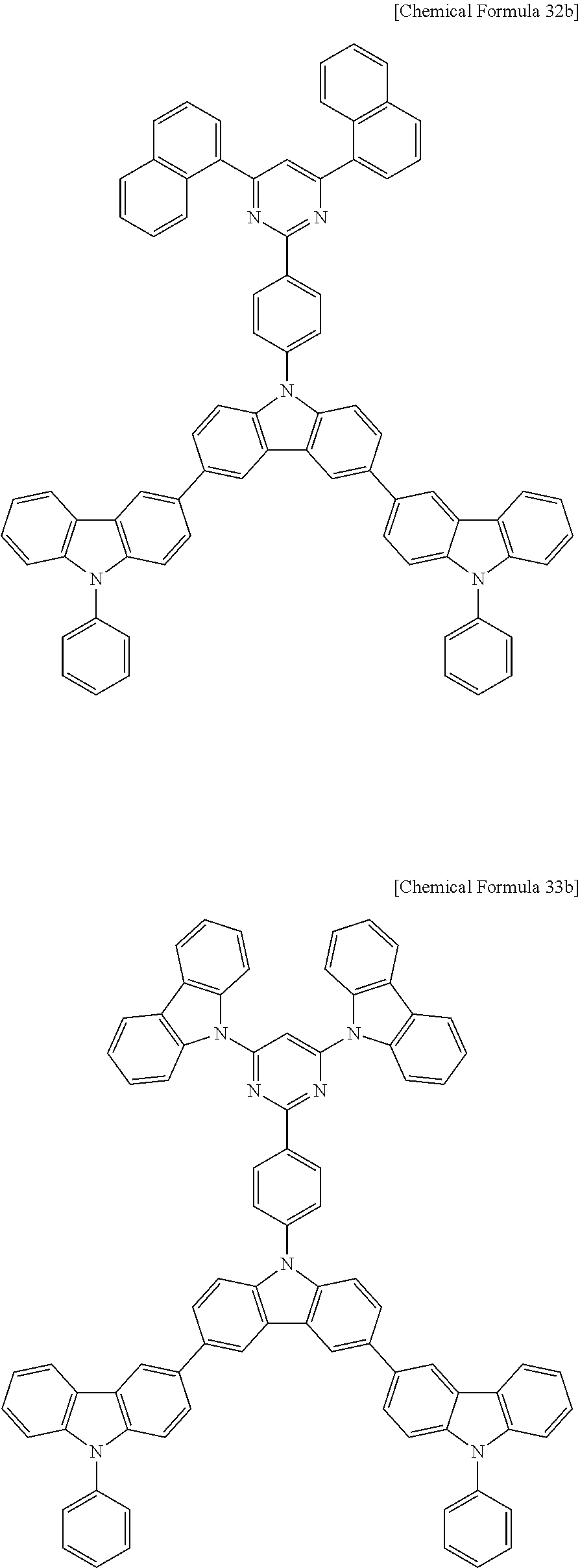
- The compound for an organic optoelectronic device may be a compound represented by, e.g., one of the following Chemical Formulae 1c to 37c.
-


- The compound for an organic optoelectronic device may be a compound represented by, e.g., one of the following Chemical Formulae 1d to 33d.
-


- The compound for an organic optoelectronic device such as the above compounds may exhibit a glass transition temperature of greater than or equal to 110° C. and a thermal decomposition temperature of greater than or equal to 400° C., indicating improved thermal stability. Thereby, it may be possible to produce an organic optoelectronic device having a high efficiency.
- The compound for an organic optoelectronic device including the above compounds may play a role for emitting light or injecting and/or transporting electrons, and also act as a light emitting host with an appropriate dopant. Thus, the compound for an organic optoelectronic device may be used as, e.g., a phosphorescent or fluorescent host material, a blue light emitting dopant material, or an electron transport material.
- The compound for an organic optoelectronic device according to an example embodiment may used for an organic thin layer, and it may improve the life-span characteristic, efficiency characteristic, electrochemical stability, and thermal stability of an organic optoelectronic device and decrease the driving voltage.
- Therefore, according to another example embodiment, an organic optoelectronic device that includes the compound for an organic optoelectronic device is provided. The organic optoelectronic device may include an organic photoelectric device, an organic light emitting diode, an organic solar cell, an organic transistor, an organic photo conductor drum, an organic memory device, and the like. For example, the compound for an organic optoelectronic device according to an example embodiment may be included in an electrode or an electrode buffer layer in the organic solar cell to improve the quantum efficiency, and it may be used as an electrode material for a gate, a source-drain electrode, or the like in the organic transistor.
- Another example embodiment provides an organic light emitting diode that includes an anode, a cathode, and at least one organic thin layer between the anode and the cathode, and the at least one organic thin layer may include the compound for an organic optoelectronic device according to an example embodiment.
- The organic thin layer that may include the compound for an organic optoelectronic device may include a layer selected from the group of an emission layer, a hole transport layer (HTL), a hole injection layer (HIL), an electron transport layer (ETL), an electron injection layer (EIL), a hole blocking layer, or a combination thereof. The at least one layer includes the compound for an organic optoelectronic device according to an example embodiment. For example, the compound for an organic optoelectronic device according to an example embodiment may be included in an electron transport layer (ETL) or an electron injection layer (EIL). In addition, when the compound for an organic optoelectronic device is included in the emission layer, the compound for an organic optoelectronic device may be included as a phosphorescent or fluorescent host, and, for example, as a fluorescent blue dopant material.
-
FIGS. 1 to 5 are cross-sectional views showing organic light emitting diodes including the compound for an organic optoelectronic device according to an example embodiment. - Referring to
FIGS. 1 to 5 , organiclight emitting diodes thin layer 105 interposed between ananode 120 and acathode 110. - The
anode 120 includes an anode material having a large work function to help hole injection into an organic thin layer. The anode material includes: a metal such as nickel, platinum, vanadium, chromium, copper, zinc, and gold, or alloys thereof; a metal oxide such as zinc oxide, indium oxide, indium tin oxide (ITO), and indium zinc oxide (IZO); a bonded metal and oxide such as ZnO:Al or SnO2:Sb; or a conductive polymer such as poly(3-methylthiophene), poly[3,4-(ethylene-1,2-dioxy)thiophene] (PEDT), polypyrrole, and polyaniline, etc. A transparent electrode including indium tin oxide (ITO) may be included an anode. - The
cathode 110 includes a cathode material having a small work function to help electron injection into an organic thin layer. The cathode material includes: a metal such as magnesium, calcium, sodium, potassium, titanium, indium, yttrium, lithium, gadolinium, aluminum, silver, tin, and lead, or alloys thereof; or a multi-layered material such as LiF/Al, Liq/Al, LiO2/Al, LiF/Ca, LiF/Al, and BaF2/Ca, etc. A metal electrode including aluminum may be included as a cathode. - Referring to
FIG. 1 , the organiclight emitting diode 100 includes an organicthin layer 105 including only anemission layer 130. - Referring to
FIG. 2 , a double-layered organiclight emitting diode 200 includes an organicthin layer 105 including anemission layer 230 including an electron transport layer (ETL), and a hole transport layer (HTL) 140. As shown inFIG. 2 , the organicthin layer 105 includes a double layer of theemission layer 230 and hole transport layer (HTL) 140. Theemission layer 130 also functions as an electron transport layer (ETL), and the hole transport layer (HTL) 140 layer may have an excellent binding property with a transparent electrode such as ITO or an excellent hole transport capability. - Referring to
FIG. 3 , a three-layered organiclight emitting diode 300 includes an organicthin layer 105 including an electron transport layer (ETL) 150, anemission layer 130, and a hole transport layer (HTL) 140. Theemission layer 130 may independently installed, and layers having an excellent electron transport capability or an excellent hole transport capability may be separately stacked. - As shown in
FIG. 4 , a four-layered organiclight emitting diode 400 includes an organicthin layer 105 including an electron injection layer (EIL) 160, anemission layer 130, a hole transport layer (HTL) 140, and a hole injection layer (HIL) 170 for adherence with the cathode of ITO. - As shown in
FIG. 5 , a five layered organiclight emitting diode 500 includes an organicthin layer 105 including an electron transport layer (ETL) 150, anemission layer 130, a hole transport layer (HTL) 140, and a hole injection layer (HIL) 170, and further includes an electron injection layer (EIL) 160 to help achieve a low voltage. - In
FIGS. 1 to 5 , the organicthin layer 105 including at least one selected from the group of an electron transport layer (ETL) 150, an electron injection layer (EIL) 160, emission layers 130 and 230, a hole transport layer (HTL) 140, a hole injection layer (HIL) 170, and combinations thereof includes a compound for an organic optoelectronic device. The compound for an organic optoelectronic device may be used for an electron transport layer (ETL) 150 including the electron transport layer (ETL) 150 or electron injection layer (EIL) 160. When it is used for the electron transport layer (ETL), it may be possible to provide an organic light emitting diode having a more simple structure because it does not require an additional hole blocking layer (not shown). - Furthermore, when the compound for an organic optoelectronic device is included in the emission layers 130 and 230, the material for the organic photoelectric device may be included as a phosphorescent or fluorescent host or a fluorescent blue dopant.
- The organic light emitting diode may be fabricated by: forming an anode on a substrate; forming an organic thin layer in accordance with a dry coating method such as evaporation, sputtering, plasma plating, and ion plating or a wet coating method such as spin coating, dipping, and flow coating; and providing a cathode thereon.
- Another example embodiment provides a display device including the organic light emitting diode according to the above embodiment.
- The following Examples and Comparative Examples are provided in order to highlight characteristics of one or more embodiments, but it will be understood that the Examples and Comparative Examples are not to be construed as limiting the scope of the embodiments, nor are the Comparative Examples to be construed as being outside the scope of the embodiments. Further, it will be understood that the embodiments are not limited to the particular details described in the Examples and Comparative Examples.
- A compound represented by the above Chemical Formula 1b as a compound for an organic optoelectronic device was synthesized according to the following Reaction Scheme 1.
-

- Synthesis Step 1
- 1.7 g (69.2 mmol) of sodium hydride (NaH) was put in a 500 mL round flask, and 50 mL of dimethylformamide (DMF) was added thereto. 15 g (46.2 mmol) of 3,6-dibromocarbazole dissolved in 100 mL of dimethylformamide was slowly added in a dropwise fashion, and then the resultant was agitated at room temperature for 40 minutes. 13.6 g (50.8 mmol) of 2-chloro-4,6-diphenyl-1,3,5-triazine dissolved in 150 mL of dimethylformamide was slowly added in a dropwise fashion, and then the resultant was agitated for 6 hours. The reactants were poured into water to complete the reaction, and a solid produced therein was filtered. The solid was washed with water and methanol and then heated and dissolved in 200 mL of toluene, and hexane was added thereto for solidification. The obtained solid was dried in a vacuum oven, obtaining 20 g of a compound A (a yield: 80%).
- Synthesis Step 2
- 9 g (16.2 mmol) of the compound A synthesized in the step 1 was mixed with 15 g (40.4 mmol) of N-phenylcarbazol-3-boronic acid pinacol ester and 200 mL of tetrahydrofuran in a 500 mL flask. 100 mL of a 2 M potassium carbonate aqueous solution and 0 0.93 g (0.08 mmol) of tetrakistriphenylphosphine palladium (0) were added and then the resultant was heated and refluxed for 12 hours under a nitrogen gas stream.
- An organic layer produced therein was separated and dried with anhydrous sodium sulfate, and an organic solvent therein was distillated and removed under a reduced pressure. The obtained product was purified through silica gel chromatography, obtaining 10 g of a compound represented by Chemical Formula 1b (a yield: 71%).
- The compound represented by Chemical Formula 1b was element-analyzed. The results are as follows.
- calcd. C63H40N6: C, 85.88; H, 4.58; N, 9.54. found: C, 85.75; H, 4.60; N, 9.61.
-

- 4.7 g (8.46 mmol) of the compound B, 3.53 g (21.15 mmol) of carbazole, and 2.44 g (25.38 mmol) of sodium tert-butoxide were put in a 250 mL round flask, and 120 mL of toluene was added thereto. The mixture was nitrogen-bubbled. 0.49 g (0.85 mmol) of palladium dibenzylideneacetone as a catalyst and 1 g of tri-tert-butylphosphine (50% in toluene) were added followed by heating up to 110° C. When the reaction was complete, a solvent in the mixture was removed, and a remaining product was heated and dissolved in chlorobenzene. The solution was charcoal-treated. After removing a solvent, the remaining product was recrystallized in chlorobenzene and hexane, obtaining 5.2 g of a compound represented by Chemical Formula 4a (a yield: 84%). The compound represented by Chemical Formula 4a was element-analyzed. The result was as follows.
- calcd. C51H32N6: C, 84.04; H, 4.43; N, 11.53. found: C, 84.15; H, 4.33; N, 11.65
-


- Synthesis Step 1
- 10 g (25.03 mmol) of 3,6-dibromo-N-phenylcarbazole, 4.6 g (27.53 mmol) of carbazole, and 3.61 g (37.55 mmol) of sodium tert-butoxide were put in a 250 mL round flask, and 150 mL of toluene was added thereto. The mixture was nitrogen-bubbled. Next, 0.43 g (0.75 mmol) of palladium dibenzylidene acetone as a catalyst and 0.8 g of tri-tert-butylphosphine (50% in toluene) were added followed by heating up to 110° C. When the reaction was complete, a solvent therein was removed, and the remaining product was heated and dissolved in chlorobenzene. The solution was charcoal-treated. The charcoal-treated solution was treated through silica gel chromatography, separating 6 g of a compound C (a yield: 50%).
- Synthesis Step 2
- 6 g (12.4 mmol) of the compound C synthesized in the step 1 and 7.82 g (14.91 mmol) of a compound D were mixed with 100 mL of tetrahydrofuran in a 250 mL flask. 50 mL of a 2 M potassium carbonate aqueous solution and 0.72 g (0.62 mmol) of tetrakistriphenyl phosphine palladium (0) were added followed by heating and refluxing for 12 hours under a nitrogen gas stream.
- The reactant was cooled down to room temperature, and a solid produced therein was filtered. The solid was washed with water and methanol and then dissolved in chlorobenzene and charcoal-treated. After removing all the solvent therein, the remaining product was recrystallized in chlorobenzene and hexane, obtaining 5.5 g of a compound represented by Chemical Formula 34c (a yield: 55%).
- The compound represented by Chemical Formula 34c was element-analyzed. The result is as follows.
- calcd. C57H36N6: C, 85.05; H, 4.51; N, 10.44. found: C, 85.55; H, 4.80; N, 10.74.
-

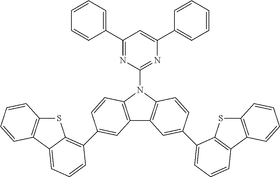
- Synthesis Step 1
- 4.05 g (101.3 mmol) of sodium hydride (NaH) was put in a 1 L round flask, and 100 mL of dimethylformamide (DMF) was added thereto. Next, a solution prepared by dissolving 21.95 g (67.5 mmol) of 3,6-dibromocarbazole in 100 mL of DMF was slowly added in a dropwise fashion and then the resultant was agitated at room temperature for 40 minutes. 21.62 g (81.0 mmol) of 2-chloro-4,6-diphenylpyrimidine was slowly added in a dropwise fashion, and the mixture was agitated for 6 hours. The resulting reactant was poured into water to complete the reaction, and a solid produced therein was filtered. The solid was washed with water and methanol and then heated and dissolve in 400 mL of chlorobenzene, and hexane was added thereto for solidification. The obtained solid was filtered and dried in a vacuum oven, obtaining 34.9 g of a compound E (a yield 93%).
- Synthesis Step 2
- 17.50 g (31.5 mmol) of the compound E synthesized in the step 1, 17.97 g (78.8 mmol) of a compound F, and 3.64 g (3.2 mmol) of tetrakistriphenyl phosphine palladium (0) were put in a 1 L flask, and 200 mL of a 2 M potassium carbonate aqueous solution and 200 mL of tetrahydrofuran and 200 mL of toluene as a solvent were added and the resultant was heated and refluxed for 12 hours under a nitrogen gas stream.
- A solid produced was filtered during the reaction. 200 mL of methanol was added to the filtered solution, and a solid additionally produced therein was filtered. The solid and the former solid were washed with 1 L of methanol. The washed solids were heated and dissolved in 100 mL of chlorobenzene, and 200 mL of methanol was added thereto for solidification. Then, the solid was dried in a vacuum oven, obtaining 10 g of a compound represented by Chemical Formula 10d (a yield: 50%).
- The compound represented by Chemical Formula 10d was element-analyzed. The result is as follows.
- calcd. C52H31N3S2: C, 81.97; H, 4.10; N, 5.51; S, 8.42. found: C, 82.34; H, 4.61; N, 5.80; S, 8.30
- A common carbazole biphenyl was used.
- The compound synthesized in Example 1 was used as a host, and Ir(PPy)3 was used as a dopant to manufacture an organic light emitting diode. 1000 Å-thick ITO was used as an anode, while 1000 Å-thick aluminum (Al) was used as a cathode.
- For example, a method of manufacturing the organic light emitting diode included cutting an ITO glass substrate having sheet resistance of 15 Ω/cm2 into a size of 50 mm×50 mm×0.7 mm and ultrasonic wave-cleaning it in acetone, isopropylalcohol, and pure water for 15 minutes respectively and then, UV-ozone cleaning it for 30 minutes.
- On the substrate, a 800 Å-thick hole transport layer (HTL) was formed by depositing N,N′-di(1-naphthyl)-N,N′-diphenylbenzidine (NPB) (70 nm) and 4,4′,4″-tri(N-carbazolyl)triphenylamine (TCTA) (10 nm) under conditions of a vacuum degree of 650×10−7 Pa and a deposition rate of 0.1 to 0.3 nm/s.
- Then, a 300 Å-thick emission layer was formed thereon using the compound according to Example 1 under the same vacuum deposit conditions, and Ir(PPy)3 as a phosphorescent dopant was simultaneously deposited. Then, a 300 Å-thick emission layer was formed thereon using the compound according to Example 2 under the same vacuum deposit conditions, and Ir(PPy)3 as a phosphorescent dopant was simultaneously deposited.
- On the emission layer, bis(8-hydroxy-2-methylquinolinolato)-aluminumbiphenoxide (BAlq) was deposit to form a 50 Å-thick hole blocking layer under the same vacuum deposit conditions.
- Subsequently, a 200 Å-thick electron transport layer (ETL) was formed thereon by depositing Alq3 under the same vacuum deposit conditions.
- On the electron transport layer (ETL), LiF and Al were sequentially deposited to form a cathode, manufacturing an organic light emitting diode.
- The organic photoelectric device had a structure of ITO/NPB (70 nm)/TCTA (10 nm)/EML (the compound of Example 1 (93 wt %)+Ir(PPy)3 (7 wt %), 30 nm)/Balq (5 nm)/Alq3 (20 nm)/LiF (1 nm)/Al (100 nm).
- An organic light emitting diode was manufactured according to the same method as Example 4 except that the compound synthesized in Example 2 was used instead of the compound synthesized in Example 1.
- An organic light emitting diode was manufactured according to the same method as Example 4 except that the compound synthesized in Example 3 was used instead of the compound synthesized in Example 1.
- An organic light emitting diode was manufactured according to the same method as Example 4 except that the compound synthesized in Comparative Example 1 was used instead of the compound synthesized in Example 1.
- Each organic light emitting diode according to Example 5 and Comparative Example 1 was measured regarding current density and luminance changes depending on voltage and luminous efficiency. The measurements were specifically performed in the following method. The results are provided in the following Table 1.
- (1) Measurement of Current Density Change Depending on Voltage Change
- The manufactured organic light emitting diodes were measured for current value flowing in the unit device while increasing the voltage from 0 V to 10 V using a current-voltage meter (Keithley 2400), and the measured current value was divided by area to provide the result.
- (2) Measurement of Luminance Change Depending on Voltage Change
- The manufactured organic light emitting diodes were measured for luminance while increasing the voltage form 0V to 10V using a luminance meter (Minolta Cs-1000A).
- (3) Measurement of Luminous Efficiency
- Current efficiency (cd/A) and electric power efficiency (lm/W) at the same luminance (1000 cd/m2) were calculated by using luminance and current density from the item (1) and (2) and voltage.
- (4) Color coordinate was measured using a luminance meter (Minolta Cs1000A), and the results are shown.
-
TABLE 1 Results at 9000 cd/m2 Driving Luminous Electric power Color Time lapsed until voltage efficiency efficiency coordinate 10% luminous (V) (cd/A) (lm/W) (x, y) efficiency decreases Example 5 4.7 50.6 33.6 0.345, 0.622 20 h Comparative 7.7 26 10.6 0.328, 0.63 1 h Example 2 - The organic light emitting diode according to Example 4 using the compound for an organic optoelectronic device of Example 1 shows about twice improved luminous efficiency and three times electric power efficiency than that of Comparative Example 2. In addition, a driving voltage may be lowered by 3 V or more.
- In terms of life-span, a time lapsed until 10% luminous efficiency decreases shows about 20 times difference. Thus, the compound of the Example 1 may improve luminous efficiency and life-span of an organic light emitting diode remarkably.
- By way of summation and review, an organic light emitting diode may convert electrical energy into light by applying current to an organic light emitting material. It may have a structure in which a functional organic material layer is interposed between an anode and a cathode. The organic material layer may include a multi-layer including different materials, for example a hole injection layer (HIL), a hole transport layer (HTL), an emission layer, an electron transport layer (ETL), and an electron injection layer (EIL), in order to improve efficiency and stability of an organic light emitting diode.
- In such an organic light emitting diode, when a voltage is applied between an anode and a cathode, holes from the anode and electrons from the cathode are injected to an organic material layer and recombined to generate excitons having high energy. The generated excitons generate light having certain wavelengths while shifting to a ground state.
- A phosphorescent light emitting material may be used for a light emitting material of an organic light emitting diode in addition to the fluorescent light emitting material. Such a phosphorescent material emits lights by transporting the electrons from a ground state to an exited state, non-radiance transiting of a singlet exciton to a triplet exciton through intersystem crossing, and transiting a triplet exciton to a ground state to emit light.
- As described above, in an organic light emitting diode, an organic material layer includes a light emitting material and a charge transport material, for example a hole injection material, a hole transport material, an electron transport material, an electron injection material, and the like.
- The light emitting material may classified as blue, green, and red light emitting materials according to emitted colors, and yellow and orange light emitting materials to emit colors approaching natural colors.
- When one material is used as a light emitting material, a maximum light emitting wavelength may shifted to a long wavelength or color purity may decrease because of interactions between molecules, or device efficiency may decrease because of a light emitting quenching effect. Therefore, a host/dopant system may be included as a light emitting material in order to improve color purity and increase luminous efficiency and stability through energy transfer.
- In order to implement excellent performance of an organic light emitting diode, a material constituting an organic material layer, for example a hole injection material, a hole transport material, a light emitting material, an electron transport material, an electron injection material, and a light emitting material such as a host and/or a dopant, should be stable and have good efficiency. However, development of an organic material layer forming material for an organic light emitting diode has thus far not been satisfactory and thus there is a need for a novel material. This material development is also required for other organic optoelectronic devices.
- A low molecular weight organic light emitting diode may be manufactured as a thin film in a vacuum deposition method, and may have good efficiency and life-span performance. A polymer organic light emitting diode manufactured in an inkjet or spin coating method has an advantage of low initial cost and being suitable for large sizes.
- Both low molecular weight organic light emitting and polymer organic light emitting diodes have an advantage of self-light emitting, high speed response, wide viewing angle, ultra-thinness, high image quality, durability, large driving temperature range, and the like. In particular, they have good visibility due to the self-light emitting characteristic compared with a conventional LCD (liquid crystal display) and have an advantage of decreasing thickness and weight of an LCD by up to a third, because they do not need a backlight.
- In addition, since they have a response speed of a microsecond unit, which may 1000 times faster than an LCD, they may realize a perfect motion picture without an after-image. Based on these advantages, they have been remarkably developed to have 80 times the efficiency and more than 100 times the life-span since they first came out in the late 1980s. Recently, they have become rapidly larger such that a 40-inch organic light emitting diode panel is now possible.
- They should simultaneously have improved luminous efficiency and life-span in order to be larger. Herein, their luminous efficiency is enhanced by smooth combination between holes and electrons in an emission layer. However, since an organic material in general may have slower electron mobility than hole mobility, it may provide less efficient combination between holes and electrons. Accordingly, increasing electron injection and mobility from a cathode and simultaneously preventing movement of holes is desired.
- As described above, embodiments may provide a compound for an organic optoelectronic device that may act as a light emitting or electron injection and transport material, and also act as a light emitting host along with an appropriate dopant.
- Embodiments may provide an organic optoelectronic device having excellent life-span, efficiency, driving voltage, electrochemical stability, and thermal stability.
- Embodiments may provide an organic optoelectronic device having excellent electrochemical and thermal stability and life-span characteristics, and high luminous efficiency at a low driving voltage.
-
<Description of symbols of drawings> 100: organic light emitting diode 110: cathode 120: anode 105: organic thin layer 130: emission layer 140: hole transport layer (HTL) 150: electron transport layer (ETL) 160: electron injection layer (EIL) 170: hole injection layer (HIL) 230: emission layer + electron transport layer (ETL) - Example embodiments have been disclosed herein, and although specific terms are employed, they are used and are to be interpreted in a generic and descriptive sense only and not for purpose of limitation. In some instances, as would be apparent to one of ordinary skill in the art as of the filing of the present application, features, characteristics, and/or elements described in connection with a particular embodiment may be used singly or in combination with features, characteristics, and/or elements described in connection with other embodiments unless otherwise specifically indicated. Accordingly, it will be understood by those of skill in the art that various changes in form and details may be made without departing from the spirit and scope as set forth in the following claims.
Claims (13)

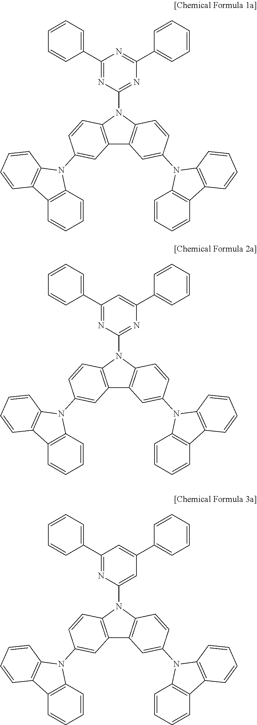


Applications Claiming Priority (3)
| Application Number | Priority Date | Filing Date | Title |
|---|---|---|---|
| KR1020100124889A KR101432599B1 (en) | 2010-08-04 | 2010-12-08 | Compound for organic photoelectric device and organic photoelectric device including the same |
| KR10-2010-0124889 | 2010-12-08 | ||
| PCT/KR2011/007539 WO2012077902A2 (en) | 2010-12-08 | 2011-10-11 | Compound for an organic optoelectronic device, organic light-emitting diode including the compound, and display device including the organic light-emitting diode |
Related Parent Applications (1)
| Application Number | Title | Priority Date | Filing Date |
|---|---|---|---|
| PCT/KR2011/007539 Continuation WO2012077902A2 (en) | 2010-12-08 | 2011-10-11 | Compound for an organic optoelectronic device, organic light-emitting diode including the compound, and display device including the organic light-emitting diode |
Publications (2)
| Publication Number | Publication Date |
|---|---|
| US20130292659A1 true US20130292659A1 (en) | 2013-11-07 |
| US9419230B2 US9419230B2 (en) | 2016-08-16 |
Family
ID=46207563
Family Applications (1)
| Application Number | Title | Priority Date | Filing Date |
|---|---|---|---|
| US13/914,008 Active 2032-11-01 US9419230B2 (en) | 2010-12-08 | 2013-06-10 | Compound for organic optoelectronic device, organic light emitting diode including the same, and display device including the organic light emitting diode |
Country Status (2)
| Country | Link |
|---|---|
| US (1) | US9419230B2 (en) |
| WO (1) | WO2012077902A2 (en) |
Cited By (22)
| Publication number | Priority date | Publication date | Assignee | Title |
|---|---|---|---|---|
| US20130204003A1 (en) * | 2011-08-18 | 2013-08-08 | Semiconductor Energy Laboratory Co., Ltd. | Carbazole compound, light-emitting element, light-emitting device, electronic device, and lighting device |
| JP2014141571A (en) * | 2013-01-23 | 2014-08-07 | Kyushu Univ | Light emitting material and organic light emitting element using the same |
| JP2014521604A (en) * | 2011-07-21 | 2014-08-28 | ローム・アンド・ハース・エレクトロニック・マテリアルズ・コリア・リミテッド | 9H-carbazole compounds and electroluminescent devices containing them |
| CN105431505A (en) * | 2013-12-18 | 2016-03-23 | 出光兴产株式会社 | Compound, material for organic electroluminescent element, ink composition, organic electroluminescent element, and electronic device |
| US9450188B2 (en) | 2010-09-21 | 2016-09-20 | Semiconductor Energy Laboratory Co., Ltd. | Carbazole derivative, light-emitting element material and organic semiconductor material |
| US20160308145A1 (en) * | 2013-11-12 | 2016-10-20 | Kyulux, Inc. | Light-emitting material, and delayed fluorescent emitter and organic light-emitting device using same |
| US20170018719A1 (en) * | 2014-03-12 | 2017-01-19 | Idemitsu Kosan Co., Ltd. | Compound, material for organic electroluminescence element, ink composition, organic electroluminescence element, and electronic device |
| CN106397415A (en) * | 2016-08-31 | 2017-02-15 | 江苏三月光电科技有限公司 | Pyridine-based five-membered-ring substituted compound and application thereof |
| CN106467518A (en) * | 2016-08-19 | 2017-03-01 | 江苏三月光电科技有限公司 | A kind of organic electroluminescent compounds with nitrogenous five-ring heterocycles as core and its application |
| US20170092872A1 (en) * | 2015-09-30 | 2017-03-30 | Samsung Electronics Co., Ltd. | Organic light-emitting device |
| CN106661001A (en) * | 2014-05-14 | 2017-05-10 | 哈佛学院院长等 | Organic light-emitting diode materials |
| US20170346017A1 (en) * | 2016-05-26 | 2017-11-30 | Samsung Display Co., Ltd. | Nitrogen-containing compound and organic electroluminescence device including the same |
| CN107880030A (en) * | 2016-09-30 | 2018-04-06 | 江苏三月光电科技有限公司 | Compound and organic electroluminescence device using triazine as core |
| JP2018061046A (en) * | 2011-08-25 | 2018-04-12 | 株式会社半導体エネルギー研究所 | Light-emitting element, light-emitting device, electronic apparatus, and lighting device |
| CN108239070A (en) * | 2016-12-27 | 2018-07-03 | 江苏三月光电科技有限公司 | It is a kind of using three carbazoles as the compound of core and its application on organic electroluminescence device |
| JP2019515488A (en) * | 2016-05-27 | 2019-06-06 | エルジー・ケム・リミテッド | Organic light emitting device |
| CN110854293A (en) * | 2018-12-10 | 2020-02-28 | 广州华睿光电材料有限公司 | Nitrogen heterocyclic compound, composition, high polymer and organic electroluminescent device |
| CN110938065A (en) * | 2018-10-31 | 2020-03-31 | 苏州大学 | Heterocycle modified carbazole-triazine derivative, preparation method and application thereof |
| CN111548342A (en) * | 2020-05-12 | 2020-08-18 | 中国科学院长春应用化学研究所 | Dendritic bipolar main body material with triazine as central core, preparation method and application of dendritic bipolar main body material in organic electroluminescent device |
| US20200313096A1 (en) * | 2019-03-26 | 2020-10-01 | Samsung Display Co., Ltd. | Organic light-emitting device and electronic apparatus |
| CN112300146A (en) * | 2019-07-30 | 2021-02-02 | 江苏三月科技股份有限公司 | Organic compound taking carbazole as core and organic electroluminescent device comprising organic compound |
| CN115960089A (en) * | 2021-10-08 | 2023-04-14 | 三星Sdi株式会社 | Compound for organic photoelectric device, and display device |
Families Citing this family (30)
| Publication number | Priority date | Publication date | Assignee | Title |
|---|---|---|---|---|
| CN102482216B (en) * | 2009-08-28 | 2014-11-19 | 保土谷化学工业株式会社 | Organic electroluminescent element and compound having carbazole ring structure |
| JP5856266B2 (en) * | 2010-09-21 | 2016-02-09 | 株式会社半導体エネルギー研究所 | Organic semiconductor device |
| KR101427611B1 (en) * | 2011-03-08 | 2014-08-11 | 롬엔드하스전자재료코리아유한회사 | Novel compounds for organic electronic material and organic electroluminescence device using the same |
| WO2013012298A1 (en) * | 2011-07-21 | 2013-01-24 | Rohm And Haas Electronic Materials Korea Ltd. | 9h-carbazole compounds and electroluminescent devices involving them |
| JPWO2013061805A1 (en) * | 2011-10-24 | 2015-04-02 | 保土谷化学工業株式会社 | Novel triphenylene derivative and organic electroluminescence device using the derivative |
| KR20130062583A (en) * | 2011-12-05 | 2013-06-13 | 롬엔드하스전자재료코리아유한회사 | Novel organic electroluminescence compounds and organic electroluminescence device using the same |
| KR20140096182A (en) * | 2012-05-02 | 2014-08-04 | 롬엔드하스전자재료코리아유한회사 | Novel Organic Electroluminescence Compounds and Organic Electroluminescence Device Containing the Same |
| JP6136616B2 (en) * | 2012-06-18 | 2017-05-31 | 東ソー株式会社 | Cyclic azine compound, method for producing the same, and organic electroluminescent device containing the same |
| WO2013191177A1 (en) * | 2012-06-18 | 2013-12-27 | 東ソー株式会社 | Cyclic azine compound, method for producing same, and organic electroluminescent element containing same |
| US9172047B2 (en) | 2012-11-30 | 2015-10-27 | Samsung Display Co., Ltd. | Hole transport material for organic electroluminescence device and organic electroluminescence device using the same |
| JP2014110276A (en) | 2012-11-30 | 2014-06-12 | Samsung Display Co Ltd | Hole transport material for organic electroluminescent element and organic electroluminescent element using the same |
| WO2014115743A1 (en) | 2013-01-23 | 2014-07-31 | 国立大学法人九州大学 | Light emitting material and organic light emitting element using same |
| JP6249151B2 (en) * | 2013-01-23 | 2017-12-20 | 株式会社Kyulux | Luminescent material and organic light emitting device using the same |
| TWI615389B (en) | 2013-03-01 | 2018-02-21 | 九州有機光材股份有限公司 | Compound, light-emitting material and organic light-emitting device |
| JP2014227399A (en) | 2013-05-24 | 2014-12-08 | 三星ディスプレイ株式會社Samsung Display Co.,Ltd. | Aryl-amine derivative and organic electroluminescent device using the same as hole transport material |
| WO2014196585A1 (en) * | 2013-06-05 | 2014-12-11 | 国立大学法人九州大学 | Luminescent material, organic luminescent element, and compound |
| US10892425B1 (en) | 2017-03-03 | 2021-01-12 | Kyulux, Inc. | Composition of matter for use in organic light-emitting diodes |
| US11283027B1 (en) | 2017-03-03 | 2022-03-22 | Kyulux, Inc. | Composition of matter for use in organic light-emitting diodes |
| US10547014B2 (en) | 2017-06-23 | 2020-01-28 | Kyulux, Inc. | Composition of matter for use in organic light-emitting diodes |
| US11069860B2 (en) | 2017-08-21 | 2021-07-20 | Kyulux, Inc. | Composition of matter for use in organic light-emitting diodes |
| US11444250B2 (en) | 2017-12-05 | 2022-09-13 | Kyulux, Inc. | Composition of matter for use in organic light-emitting diodes |
| US11575088B2 (en) | 2017-12-22 | 2023-02-07 | Kyulux, Inc. | Composition of matter for use in organic light-emitting diodes |
| US10644249B2 (en) | 2017-12-22 | 2020-05-05 | Kyulux, Inc. | Composition of matter for use in organic light-emitting diodes |
| US11542260B2 (en) | 2018-01-31 | 2023-01-03 | Kyulux, Inc. | Composition of matter for use in organic light-emitting diodes |
| US11104669B2 (en) | 2018-02-02 | 2021-08-31 | Kyulux, Inc. | Composition of matter for use in organic light-emitting diodes |
| US11608333B2 (en) | 2018-03-20 | 2023-03-21 | Kyulux, Inc. | Composition of matter for use in organic light-emitting diodes |
| US11498914B2 (en) | 2018-03-30 | 2022-11-15 | Kyulux, Inc. | Composition of matter for use in organic light-emitting diodes |
| US11778904B2 (en) | 2018-05-09 | 2023-10-03 | Kyulux, Inc. | Composition of matter for use in organic light-emitting diodes |
| CN108912154B (en) * | 2018-08-03 | 2021-04-16 | 大连理工大学 | Base material for preparing bipolar electroluminescent material |
| CN108752372B (en) * | 2018-08-03 | 2021-01-22 | 大连理工大学 | Compound for preparing organic electroluminescent material |
Citations (2)
| Publication number | Priority date | Publication date | Assignee | Title |
|---|---|---|---|---|
| US20040164292A1 (en) * | 2003-02-21 | 2004-08-26 | Yeh-Jiun Tung | Transflective display having an OLED backlight |
| JP2009267255A (en) * | 2008-04-28 | 2009-11-12 | Idemitsu Kosan Co Ltd | Material for organic electroluminescent element and organic electroluminescent element using the material |
Family Cites Families (14)
| Publication number | Priority date | Publication date | Assignee | Title |
|---|---|---|---|---|
| US6660410B2 (en) | 2000-03-27 | 2003-12-09 | Idemitsu Kosan Co., Ltd. | Organic electroluminescence element |
| JP2002302516A (en) | 2001-04-03 | 2002-10-18 | Fuji Photo Film Co Ltd | New polymer and light-emitting element using the same |
| JP2004018787A (en) * | 2002-06-19 | 2004-01-22 | Fuji Photo Film Co Ltd | Carbazole derivative, polymer of the same and light-emitting element containing the same |
| JP4707082B2 (en) | 2002-11-26 | 2011-06-22 | コニカミノルタホールディングス株式会社 | Organic electroluminescence element and display device |
| CN101171239B (en) | 2005-04-28 | 2013-08-14 | 西巴特殊化学品控股有限公司 | Electroluminescent device |
| US20080269461A1 (en) | 2005-12-20 | 2008-10-30 | Koninklijke Philips Electronics, N.V. | Polymeric Carbazole Compounds |
| CN101657517B (en) | 2007-04-13 | 2013-03-27 | 第一毛织株式会社 | Material for organic photoelectric device including electron transporting unit and hole transporting unit, and organic photoelectric device including the same |
| JP5194596B2 (en) | 2007-07-11 | 2013-05-08 | コニカミノルタホールディングス株式会社 | Organic electroluminescence element, display device and lighting device |
| KR20090028943A (en) * | 2007-09-17 | 2009-03-20 | (주)루디스 | Hole injection/transporting layer material and organic electroluminescent device comprising same |
| JP5593696B2 (en) | 2007-11-08 | 2014-09-24 | コニカミノルタ株式会社 | Method for manufacturing organic electroluminescence device |
| WO2009060780A1 (en) | 2007-11-08 | 2009-05-14 | Konica Minolta Holdings, Inc. | Organic electroluminescence element, display device, and lighting system |
| KR100931067B1 (en) | 2007-11-19 | 2009-12-10 | 제일모직주식회사 | Organometallic Complex Compound for Organic Photoelectric Device and Organic Photoelectric Device Comprising the Same |
| JP2009267257A (en) * | 2008-04-28 | 2009-11-12 | Idemitsu Kosan Co Ltd | Material for organic electroluminescent element and organic electroluminescent element using the material |
| JP2009263579A (en) * | 2008-04-28 | 2009-11-12 | Idemitsu Kosan Co Ltd | Material for organic electroluminescent element and organic electroluminescent element using it |
-
2011
- 2011-10-11 WO PCT/KR2011/007539 patent/WO2012077902A2/en active Application Filing
-
2013
- 2013-06-10 US US13/914,008 patent/US9419230B2/en active Active
Patent Citations (2)
| Publication number | Priority date | Publication date | Assignee | Title |
|---|---|---|---|---|
| US20040164292A1 (en) * | 2003-02-21 | 2004-08-26 | Yeh-Jiun Tung | Transflective display having an OLED backlight |
| JP2009267255A (en) * | 2008-04-28 | 2009-11-12 | Idemitsu Kosan Co Ltd | Material for organic electroluminescent element and organic electroluminescent element using the material |
Non-Patent Citations (1)
| Title |
|---|
| Promarak et al., Synthesis and properties of stable amorphous hole-transporting molecules for electroluminescent devices, 2006, Tetrahedron Letters, Vol. 47, pages 8949-8952. * |
Cited By (37)
| Publication number | Priority date | Publication date | Assignee | Title |
|---|---|---|---|---|
| US9450188B2 (en) | 2010-09-21 | 2016-09-20 | Semiconductor Energy Laboratory Co., Ltd. | Carbazole derivative, light-emitting element material and organic semiconductor material |
| US10071993B2 (en) | 2010-09-21 | 2018-09-11 | Semiconductor Energy Laboratory Co., Ltd. | Carbazole derivative, light-emitting element material and organic semiconductor material |
| JP2014521604A (en) * | 2011-07-21 | 2014-08-28 | ローム・アンド・ハース・エレクトロニック・マテリアルズ・コリア・リミテッド | 9H-carbazole compounds and electroluminescent devices containing them |
| US9799834B2 (en) | 2011-08-18 | 2017-10-24 | Semiconductor Energy Laboratory Co., Ltd. | Carbazole compound light-emitting element, light-emitting device, electronic device, and lighting device |
| US9029558B2 (en) * | 2011-08-18 | 2015-05-12 | Semiconductor Energy Laboratory Co., Ltd. | Carbazole compound, light-emitting element, light-emitting device, electronic device, and lighting device |
| US20130204003A1 (en) * | 2011-08-18 | 2013-08-08 | Semiconductor Energy Laboratory Co., Ltd. | Carbazole compound, light-emitting element, light-emitting device, electronic device, and lighting device |
| US11008510B2 (en) | 2011-08-25 | 2021-05-18 | Semiconductor Energy Laboratory Co., Ltd. | Light-emitting element, light-emitting device, electronic device, lighting device, and novel organic compound |
| JP2018061046A (en) * | 2011-08-25 | 2018-04-12 | 株式会社半導体エネルギー研究所 | Light-emitting element, light-emitting device, electronic apparatus, and lighting device |
| US11773321B2 (en) | 2011-08-25 | 2023-10-03 | Semiconductor Energy Laboratory Co., Ltd. | Light-emitting element, light-emitting device, electronic device, lighting device, and novel organic compound |
| JP2014141571A (en) * | 2013-01-23 | 2014-08-07 | Kyushu Univ | Light emitting material and organic light emitting element using the same |
| US20160308145A1 (en) * | 2013-11-12 | 2016-10-20 | Kyulux, Inc. | Light-emitting material, and delayed fluorescent emitter and organic light-emitting device using same |
| US11101433B2 (en) * | 2013-11-12 | 2021-08-24 | Kyulux, Inc. | Light-emitting material, and delayed fluorescent emitter and organic light-emitting device using same |
| US20160329505A1 (en) * | 2013-12-18 | 2016-11-10 | Idemitsu Kosan Co., Ltd. | Compound, material for organic electroluminescent elements, ink composition, organic electroluminescent element and electronic device |
| CN105431505A (en) * | 2013-12-18 | 2016-03-23 | 出光兴产株式会社 | Compound, material for organic electroluminescent element, ink composition, organic electroluminescent element, and electronic device |
| US20170018719A1 (en) * | 2014-03-12 | 2017-01-19 | Idemitsu Kosan Co., Ltd. | Compound, material for organic electroluminescence element, ink composition, organic electroluminescence element, and electronic device |
| CN106661001A (en) * | 2014-05-14 | 2017-05-10 | 哈佛学院院长等 | Organic light-emitting diode materials |
| JP2017518281A (en) * | 2014-05-14 | 2017-07-06 | プレジデント アンド フェローズ オブ ハーバード カレッジ | Organic light emitting diode material |
| US20170244049A1 (en) * | 2014-05-14 | 2017-08-24 | President And Fellows Of Harvard College | Organic light-emitting diode materials |
| US20170092872A1 (en) * | 2015-09-30 | 2017-03-30 | Samsung Electronics Co., Ltd. | Organic light-emitting device |
| US10651392B2 (en) * | 2015-09-30 | 2020-05-12 | Samsung Electronics Co., Ltd. | Organic light-emitting device |
| US20170346017A1 (en) * | 2016-05-26 | 2017-11-30 | Samsung Display Co., Ltd. | Nitrogen-containing compound and organic electroluminescence device including the same |
| JP2017210464A (en) * | 2016-05-26 | 2017-11-30 | 三星ディスプレイ株式會社Samsung Display Co.,Ltd. | Nitrogen-containing compound and organic electroluminescence device including the same |
| US10686139B2 (en) * | 2016-05-26 | 2020-06-16 | Samsung Display Co., Ltd. | Nitrogen-containing compound and organic electroluminescence device including the same |
| JP2019515488A (en) * | 2016-05-27 | 2019-06-06 | エルジー・ケム・リミテッド | Organic light emitting device |
| CN109354588A (en) * | 2016-08-19 | 2019-02-19 | 江苏三月光电科技有限公司 | It is a kind of using nitrogenous five-ring heterocycles as the organic electroluminescent compounds of core and its application |
| CN109354588B (en) * | 2016-08-19 | 2021-04-27 | 中节能万润股份有限公司 | Organic electroluminescent compound with nitrogen-containing five-membered heterocyclic ring as core and application thereof |
| CN106467518A (en) * | 2016-08-19 | 2017-03-01 | 江苏三月光电科技有限公司 | A kind of organic electroluminescent compounds with nitrogenous five-ring heterocycles as core and its application |
| CN106397415A (en) * | 2016-08-31 | 2017-02-15 | 江苏三月光电科技有限公司 | Pyridine-based five-membered-ring substituted compound and application thereof |
| CN107880030A (en) * | 2016-09-30 | 2018-04-06 | 江苏三月光电科技有限公司 | Compound and organic electroluminescence device using triazine as core |
| CN108239070A (en) * | 2016-12-27 | 2018-07-03 | 江苏三月光电科技有限公司 | It is a kind of using three carbazoles as the compound of core and its application on organic electroluminescence device |
| CN110938065A (en) * | 2018-10-31 | 2020-03-31 | 苏州大学 | Heterocycle modified carbazole-triazine derivative, preparation method and application thereof |
| CN110854293A (en) * | 2018-12-10 | 2020-02-28 | 广州华睿光电材料有限公司 | Nitrogen heterocyclic compound, composition, high polymer and organic electroluminescent device |
| US20200313096A1 (en) * | 2019-03-26 | 2020-10-01 | Samsung Display Co., Ltd. | Organic light-emitting device and electronic apparatus |
| EP3739644A3 (en) * | 2019-03-26 | 2021-02-17 | Samsung Display Co., Ltd. | Organic light-emitting device and electronic apparatus |
| CN112300146A (en) * | 2019-07-30 | 2021-02-02 | 江苏三月科技股份有限公司 | Organic compound taking carbazole as core and organic electroluminescent device comprising organic compound |
| CN111548342A (en) * | 2020-05-12 | 2020-08-18 | 中国科学院长春应用化学研究所 | Dendritic bipolar main body material with triazine as central core, preparation method and application of dendritic bipolar main body material in organic electroluminescent device |
| CN115960089A (en) * | 2021-10-08 | 2023-04-14 | 三星Sdi株式会社 | Compound for organic photoelectric device, and display device |
Also Published As
| Publication number | Publication date |
|---|---|
| WO2012077902A9 (en) | 2013-10-31 |
| WO2012077902A3 (en) | 2012-08-16 |
| WO2012077902A2 (en) | 2012-06-14 |
| US9419230B2 (en) | 2016-08-16 |
Similar Documents
| Publication | Publication Date | Title |
|---|---|---|
| US9419230B2 (en) | Compound for organic optoelectronic device, organic light emitting diode including the same, and display device including the organic light emitting diode | |
| US9559309B2 (en) | Compound for organic optoelectronic device, organic light emitting diode including the same, and display device including the organic light emitting diode | |
| US10121973B2 (en) | Compound for organic optoelectronic device, organic light-emitting diode including same, and display device including organic light-emitting diode | |
| EP2796530B2 (en) | Compound for an organic optoelectronic element, organic light-emitting element comprising same, and display device comprising the organic light-emitting element | |
| US9543530B2 (en) | Compound for organic optoelectronic device, organic light emitting diode including the same and display including the organic light emitting diode | |
| US9450193B2 (en) | Compound for organic photoelectric device and organic photoelectric device including the same | |
| US9548460B2 (en) | Compound for organic optoelectronic device, organic light emitting diode including the same and display including the organic light emitting diode | |
| KR101739612B1 (en) | Fluoranthene compound and organic electronic device comprising the same | |
| US8530063B2 (en) | Compound for organic photoelectric device and organic photoelectric device including the same | |
| US8697257B2 (en) | Compound for organic photoelectric device, organic photoelectric device including the same, and display device including the organic photoelectric device | |
| US9136481B2 (en) | Compound for an organic photoelectric device, organic photoelectric device including the same, and display device including the organic photoelectric device | |
| US9012039B2 (en) | Compound for organic photoelectric device and organic photoelectric device including the same | |
| US20130256644A1 (en) | Compound for organic optoelectronic device, organic light emitting diode including the same and display including the organic light emitting diode | |
| EP2508585B1 (en) | Compound for organic optoelectronic device, organic light emitting diode including the same, and display device including organic light emitting diode | |
| US20150263294A1 (en) | Compound for organic optoelectronic device, organic light-emitting device including same, and display device including the organic light- emitting diode | |
| EP2842954A1 (en) | Compound for organic optoelectric device, organic light emitting device containing same, and display device containing said organic light emitting device | |
| US20150144937A1 (en) | Compound for organic optoelectronic device, organic light emitting diode comprising same, and display device comprising organic light emitting diode | |
| US9444054B2 (en) | Compound for organic optoelectronic device and organic light emitting diode including the same | |
| US20130299794A1 (en) | Compound for organic optoelectronic device, organic light emitting diode including the same and display including the organic light emitting diode | |
| US9793488B2 (en) | Compound for organic optoelectronic element, organic light-emitting element comprising same, and display device comprising the organic light-emitting element | |
| US9540374B2 (en) | Nitrogen-containing heterocyclic compounds and organic electronic device comprising the same | |
| US20150021563A1 (en) | Compound for organic optoelectronic device, organic light emitting diode including the same and display including the organic light emitting diode | |
| KR20190089764A (en) | Multicyclic compound and organic light emitting device comprising the same | |
| US20130285030A1 (en) | Compound for organic optoelectronic device, organic light emitting diode including the same, and display device including the organic light emitting diode | |
| US9825242B2 (en) | Compound for organic optoelectric device, organic light-emitting diode including same, display device including organic light-emitting diode |
Legal Events
| Date | Code | Title | Description |
|---|---|---|---|
| AS | Assignment |
Owner name: CHEIL INDUSTRIES, INC., KOREA, REPUBLIC OF Free format text: ASSIGNMENT OF ASSIGNORS INTEREST;ASSIGNORS:KIM, HYUNG-SUN;YU, EUN-SUN;CHAE, MI-YOUNG;REEL/FRAME:030579/0774 Effective date: 20130605 |
|
| STCF | Information on status: patent grant |
Free format text: PATENTED CASE |
|
| MAFP | Maintenance fee payment |
Free format text: PAYMENT OF MAINTENANCE FEE, 4TH YEAR, LARGE ENTITY (ORIGINAL EVENT CODE: M1551); ENTITY STATUS OF PATENT OWNER: LARGE ENTITY Year of fee payment: 4 |
|
| MAFP | Maintenance fee payment |
Free format text: PAYMENT OF MAINTENANCE FEE, 8TH YEAR, LARGE ENTITY (ORIGINAL EVENT CODE: M1552); ENTITY STATUS OF PATENT OWNER: LARGE ENTITY Year of fee payment: 8 |