US9780265B2 - Optoelectronic semiconductor component - Google Patents
Optoelectronic semiconductor component Download PDFInfo
- Publication number
- US9780265B2 US9780265B2 US15/117,177 US201515117177A US9780265B2 US 9780265 B2 US9780265 B2 US 9780265B2 US 201515117177 A US201515117177 A US 201515117177A US 9780265 B2 US9780265 B2 US 9780265B2
- Authority
- US
- United States
- Prior art keywords
- optoelectronic semiconductor
- layer
- connection carrier
- growth substrate
- semiconductor component
- Prior art date
- Legal status (The legal status is an assumption and is not a legal conclusion. Google has not performed a legal analysis and makes no representation as to the accuracy of the status listed.)
- Active
Links
- 239000004065 semiconductor Substances 0.000 title claims abstract description 240
- 230000005693 optoelectronics Effects 0.000 title claims abstract description 185
- 239000000758 substrate Substances 0.000 claims abstract description 88
- 238000006243 chemical reaction Methods 0.000 claims abstract description 85
- 238000009413 insulation Methods 0.000 claims abstract description 61
- 238000001465 metallisation Methods 0.000 claims description 35
- 238000000034 method Methods 0.000 claims description 26
- 230000005670 electromagnetic radiation Effects 0.000 claims description 21
- 238000004519 manufacturing process Methods 0.000 claims description 16
- 239000000463 material Substances 0.000 claims description 15
- 239000012777 electrically insulating material Substances 0.000 claims description 4
- 239000000969 carrier Substances 0.000 claims description 3
- 230000005855 radiation Effects 0.000 claims description 3
- 238000005538 encapsulation Methods 0.000 description 8
- BASFCYQUMIYNBI-UHFFFAOYSA-N platinum Chemical compound [Pt] BASFCYQUMIYNBI-UHFFFAOYSA-N 0.000 description 8
- 229910052709 silver Inorganic materials 0.000 description 7
- 239000004332 silver Substances 0.000 description 7
- 230000001681 protective effect Effects 0.000 description 6
- 229910000679 solder Inorganic materials 0.000 description 6
- PCHJSUWPFVWCPO-UHFFFAOYSA-N gold Chemical compound [Au] PCHJSUWPFVWCPO-UHFFFAOYSA-N 0.000 description 5
- 229910052737 gold Inorganic materials 0.000 description 5
- 239000010931 gold Substances 0.000 description 5
- 239000002245 particle Substances 0.000 description 5
- 238000002161 passivation Methods 0.000 description 5
- OAICVXFJPJFONN-UHFFFAOYSA-N Phosphorus Chemical compound [P] OAICVXFJPJFONN-UHFFFAOYSA-N 0.000 description 4
- VYPSYNLAJGMNEJ-UHFFFAOYSA-N Silicium dioxide Chemical compound O=[Si]=O VYPSYNLAJGMNEJ-UHFFFAOYSA-N 0.000 description 4
- RTAQQCXQSZGOHL-UHFFFAOYSA-N Titanium Chemical compound [Ti] RTAQQCXQSZGOHL-UHFFFAOYSA-N 0.000 description 4
- 229910052697 platinum Inorganic materials 0.000 description 4
- 238000004382 potting Methods 0.000 description 4
- 229910052719 titanium Inorganic materials 0.000 description 4
- 239000010936 titanium Substances 0.000 description 4
- 229910052751 metal Inorganic materials 0.000 description 3
- 239000002184 metal Substances 0.000 description 3
- 238000007788 roughening Methods 0.000 description 3
- 229910052581 Si3N4 Inorganic materials 0.000 description 2
- BQCADISMDOOEFD-UHFFFAOYSA-N Silver Chemical compound [Ag] BQCADISMDOOEFD-UHFFFAOYSA-N 0.000 description 2
- 239000004020 conductor Substances 0.000 description 2
- 230000008569 process Effects 0.000 description 2
- 235000012239 silicon dioxide Nutrition 0.000 description 2
- 239000000377 silicon dioxide Substances 0.000 description 2
- HQVNEWCFYHHQES-UHFFFAOYSA-N silicon nitride Chemical compound N12[Si]34N5[Si]62N3[Si]51N64 HQVNEWCFYHHQES-UHFFFAOYSA-N 0.000 description 2
- 230000000087 stabilizing effect Effects 0.000 description 2
- RYGMFSIKBFXOCR-UHFFFAOYSA-N Copper Chemical compound [Cu] RYGMFSIKBFXOCR-UHFFFAOYSA-N 0.000 description 1
- 229910002601 GaN Inorganic materials 0.000 description 1
- JMASRVWKEDWRBT-UHFFFAOYSA-N Gallium nitride Chemical compound [Ga]#N JMASRVWKEDWRBT-UHFFFAOYSA-N 0.000 description 1
- ATJFFYVFTNAWJD-UHFFFAOYSA-N Tin Chemical compound [Sn] ATJFFYVFTNAWJD-UHFFFAOYSA-N 0.000 description 1
- 229910052782 aluminium Inorganic materials 0.000 description 1
- XAGFODPZIPBFFR-UHFFFAOYSA-N aluminium Chemical compound [Al] XAGFODPZIPBFFR-UHFFFAOYSA-N 0.000 description 1
- 230000004888 barrier function Effects 0.000 description 1
- 239000003990 capacitor Substances 0.000 description 1
- 239000000919 ceramic Substances 0.000 description 1
- 229910010293 ceramic material Inorganic materials 0.000 description 1
- 229910052802 copper Inorganic materials 0.000 description 1
- 239000010949 copper Substances 0.000 description 1
- 230000008878 coupling Effects 0.000 description 1
- 238000010168 coupling process Methods 0.000 description 1
- 238000005859 coupling reaction Methods 0.000 description 1
- 238000005520 cutting process Methods 0.000 description 1
- 238000013461 design Methods 0.000 description 1
- 238000009792 diffusion process Methods 0.000 description 1
- 238000009826 distribution Methods 0.000 description 1
- 238000010292 electrical insulation Methods 0.000 description 1
- 238000001962 electrophoresis Methods 0.000 description 1
- 238000011990 functional testing Methods 0.000 description 1
- 239000011810 insulating material Substances 0.000 description 1
- 230000010354 integration Effects 0.000 description 1
- 230000001788 irregular Effects 0.000 description 1
- 239000011159 matrix material Substances 0.000 description 1
- 230000005012 migration Effects 0.000 description 1
- 238000013508 migration Methods 0.000 description 1
- 230000035515 penetration Effects 0.000 description 1
- 229920001296 polysiloxane Polymers 0.000 description 1
- 229910052594 sapphire Inorganic materials 0.000 description 1
- 239000010980 sapphire Substances 0.000 description 1
- 229910052710 silicon Inorganic materials 0.000 description 1
- 239000010703 silicon Substances 0.000 description 1
- HBMJWWWQQXIZIP-UHFFFAOYSA-N silicon carbide Chemical compound [Si+]#[C-] HBMJWWWQQXIZIP-UHFFFAOYSA-N 0.000 description 1
- 229910010271 silicon carbide Inorganic materials 0.000 description 1
- 238000005507 spraying Methods 0.000 description 1
- -1 titanium tungsten nitride Chemical class 0.000 description 1
- 238000012546 transfer Methods 0.000 description 1
Images


Classifications
-
- H—ELECTRICITY
- H01—ELECTRIC ELEMENTS
- H01L—SEMICONDUCTOR DEVICES NOT COVERED BY CLASS H10
- H01L33/00—Semiconductor devices having potential barriers specially adapted for light emission; Processes or apparatus specially adapted for the manufacture or treatment thereof or of parts thereof; Details thereof
- H01L33/48—Semiconductor devices having potential barriers specially adapted for light emission; Processes or apparatus specially adapted for the manufacture or treatment thereof or of parts thereof; Details thereof characterised by the semiconductor body packages
- H01L33/50—Wavelength conversion elements
- H01L33/505—Wavelength conversion elements characterised by the shape, e.g. plate or foil
-
- H—ELECTRICITY
- H01—ELECTRIC ELEMENTS
- H01L—SEMICONDUCTOR DEVICES NOT COVERED BY CLASS H10
- H01L25/00—Assemblies consisting of a plurality of individual semiconductor or other solid state devices ; Multistep manufacturing processes thereof
- H01L25/16—Assemblies consisting of a plurality of individual semiconductor or other solid state devices ; Multistep manufacturing processes thereof the devices being of types provided for in two or more different main groups of groups H01L27/00 - H01L33/00, or in a single subclass of H10K, H10N, e.g. forming hybrid circuits
- H01L25/167—Assemblies consisting of a plurality of individual semiconductor or other solid state devices ; Multistep manufacturing processes thereof the devices being of types provided for in two or more different main groups of groups H01L27/00 - H01L33/00, or in a single subclass of H10K, H10N, e.g. forming hybrid circuits comprising optoelectronic devices, e.g. LED, photodiodes
-
- H—ELECTRICITY
- H01—ELECTRIC ELEMENTS
- H01L—SEMICONDUCTOR DEVICES NOT COVERED BY CLASS H10
- H01L33/00—Semiconductor devices having potential barriers specially adapted for light emission; Processes or apparatus specially adapted for the manufacture or treatment thereof or of parts thereof; Details thereof
- H01L33/005—Processes
- H01L33/0095—Post-treatment of devices, e.g. annealing, recrystallisation or short-circuit elimination
-
- H—ELECTRICITY
- H01—ELECTRIC ELEMENTS
- H01L—SEMICONDUCTOR DEVICES NOT COVERED BY CLASS H10
- H01L33/00—Semiconductor devices having potential barriers specially adapted for light emission; Processes or apparatus specially adapted for the manufacture or treatment thereof or of parts thereof; Details thereof
- H01L33/36—Semiconductor devices having potential barriers specially adapted for light emission; Processes or apparatus specially adapted for the manufacture or treatment thereof or of parts thereof; Details thereof characterised by the electrodes
- H01L33/40—Materials therefor
- H01L33/405—Reflective materials
-
- H—ELECTRICITY
- H01—ELECTRIC ELEMENTS
- H01L—SEMICONDUCTOR DEVICES NOT COVERED BY CLASS H10
- H01L33/00—Semiconductor devices having potential barriers specially adapted for light emission; Processes or apparatus specially adapted for the manufacture or treatment thereof or of parts thereof; Details thereof
- H01L33/48—Semiconductor devices having potential barriers specially adapted for light emission; Processes or apparatus specially adapted for the manufacture or treatment thereof or of parts thereof; Details thereof characterised by the semiconductor body packages
- H01L33/483—Containers
- H01L33/486—Containers adapted for surface mounting
-
- H—ELECTRICITY
- H01—ELECTRIC ELEMENTS
- H01L—SEMICONDUCTOR DEVICES NOT COVERED BY CLASS H10
- H01L33/00—Semiconductor devices having potential barriers specially adapted for light emission; Processes or apparatus specially adapted for the manufacture or treatment thereof or of parts thereof; Details thereof
- H01L33/48—Semiconductor devices having potential barriers specially adapted for light emission; Processes or apparatus specially adapted for the manufacture or treatment thereof or of parts thereof; Details thereof characterised by the semiconductor body packages
- H01L33/58—Optical field-shaping elements
- H01L33/60—Reflective elements
-
- H—ELECTRICITY
- H01—ELECTRIC ELEMENTS
- H01L—SEMICONDUCTOR DEVICES NOT COVERED BY CLASS H10
- H01L33/00—Semiconductor devices having potential barriers specially adapted for light emission; Processes or apparatus specially adapted for the manufacture or treatment thereof or of parts thereof; Details thereof
- H01L33/48—Semiconductor devices having potential barriers specially adapted for light emission; Processes or apparatus specially adapted for the manufacture or treatment thereof or of parts thereof; Details thereof characterised by the semiconductor body packages
- H01L33/62—Arrangements for conducting electric current to or from the semiconductor body, e.g. lead-frames, wire-bonds or solder balls
-
- H—ELECTRICITY
- H01—ELECTRIC ELEMENTS
- H01L—SEMICONDUCTOR DEVICES NOT COVERED BY CLASS H10
- H01L25/00—Assemblies consisting of a plurality of individual semiconductor or other solid state devices ; Multistep manufacturing processes thereof
- H01L25/03—Assemblies consisting of a plurality of individual semiconductor or other solid state devices ; Multistep manufacturing processes thereof all the devices being of a type provided for in the same subgroup of groups H01L27/00 - H01L33/00, or in a single subclass of H10K, H10N, e.g. assemblies of rectifier diodes
- H01L25/04—Assemblies consisting of a plurality of individual semiconductor or other solid state devices ; Multistep manufacturing processes thereof all the devices being of a type provided for in the same subgroup of groups H01L27/00 - H01L33/00, or in a single subclass of H10K, H10N, e.g. assemblies of rectifier diodes the devices not having separate containers
- H01L25/075—Assemblies consisting of a plurality of individual semiconductor or other solid state devices ; Multistep manufacturing processes thereof all the devices being of a type provided for in the same subgroup of groups H01L27/00 - H01L33/00, or in a single subclass of H10K, H10N, e.g. assemblies of rectifier diodes the devices not having separate containers the devices being of a type provided for in group H01L33/00
- H01L25/0753—Assemblies consisting of a plurality of individual semiconductor or other solid state devices ; Multistep manufacturing processes thereof all the devices being of a type provided for in the same subgroup of groups H01L27/00 - H01L33/00, or in a single subclass of H10K, H10N, e.g. assemblies of rectifier diodes the devices not having separate containers the devices being of a type provided for in group H01L33/00 the devices being arranged next to each other
-
- H—ELECTRICITY
- H01—ELECTRIC ELEMENTS
- H01L—SEMICONDUCTOR DEVICES NOT COVERED BY CLASS H10
- H01L2924/00—Indexing scheme for arrangements or methods for connecting or disconnecting semiconductor or solid-state bodies as covered by H01L24/00
-
- H—ELECTRICITY
- H01—ELECTRIC ELEMENTS
- H01L—SEMICONDUCTOR DEVICES NOT COVERED BY CLASS H10
- H01L2924/00—Indexing scheme for arrangements or methods for connecting or disconnecting semiconductor or solid-state bodies as covered by H01L24/00
- H01L2924/0001—Technical content checked by a classifier
- H01L2924/0002—Not covered by any one of groups H01L24/00, H01L24/00 and H01L2224/00
-
- H—ELECTRICITY
- H01—ELECTRIC ELEMENTS
- H01L—SEMICONDUCTOR DEVICES NOT COVERED BY CLASS H10
- H01L2933/00—Details relating to devices covered by the group H01L33/00 but not provided for in its subgroups
- H01L2933/0008—Processes
- H01L2933/0033—Processes relating to semiconductor body packages
- H01L2933/0041—Processes relating to semiconductor body packages relating to wavelength conversion elements
-
- H—ELECTRICITY
- H01—ELECTRIC ELEMENTS
- H01L—SEMICONDUCTOR DEVICES NOT COVERED BY CLASS H10
- H01L2933/00—Details relating to devices covered by the group H01L33/00 but not provided for in its subgroups
- H01L2933/0008—Processes
- H01L2933/0033—Processes relating to semiconductor body packages
- H01L2933/0066—Processes relating to semiconductor body packages relating to arrangements for conducting electric current to or from the semiconductor body
-
- H01L33/0079—
-
- H—ELECTRICITY
- H01—ELECTRIC ELEMENTS
- H01L—SEMICONDUCTOR DEVICES NOT COVERED BY CLASS H10
- H01L33/00—Semiconductor devices having potential barriers specially adapted for light emission; Processes or apparatus specially adapted for the manufacture or treatment thereof or of parts thereof; Details thereof
- H01L33/005—Processes
- H01L33/0093—Wafer bonding; Removal of the growth substrate
-
- H—ELECTRICITY
- H01—ELECTRIC ELEMENTS
- H01L—SEMICONDUCTOR DEVICES NOT COVERED BY CLASS H10
- H01L33/00—Semiconductor devices having potential barriers specially adapted for light emission; Processes or apparatus specially adapted for the manufacture or treatment thereof or of parts thereof; Details thereof
- H01L33/02—Semiconductor devices having potential barriers specially adapted for light emission; Processes or apparatus specially adapted for the manufacture or treatment thereof or of parts thereof; Details thereof characterised by the semiconductor bodies
- H01L33/10—Semiconductor devices having potential barriers specially adapted for light emission; Processes or apparatus specially adapted for the manufacture or treatment thereof or of parts thereof; Details thereof characterised by the semiconductor bodies with a light reflecting structure, e.g. semiconductor Bragg reflector
-
- H—ELECTRICITY
- H01—ELECTRIC ELEMENTS
- H01L—SEMICONDUCTOR DEVICES NOT COVERED BY CLASS H10
- H01L33/00—Semiconductor devices having potential barriers specially adapted for light emission; Processes or apparatus specially adapted for the manufacture or treatment thereof or of parts thereof; Details thereof
- H01L33/44—Semiconductor devices having potential barriers specially adapted for light emission; Processes or apparatus specially adapted for the manufacture or treatment thereof or of parts thereof; Details thereof characterised by the coatings, e.g. passivation layer or anti-reflective coating
- H01L33/46—Reflective coating, e.g. dielectric Bragg reflector
Definitions
- the present application relates to an optoelectronic semiconductor component.
- One object to be achieved consists in specifying a compact, volume emitting and white converting optoelectronic semiconductor component.
- the optoelectronic semiconductor component can be for example a light emitting diode or a laser diode.
- the optoelectronic semiconductor component comprises an optoelectronic semiconductor chip provided for emitting electromagnetic radiation.
- the optoelectronic semiconductor chip can be for example a light emitting diode chip or a laser diode chip.
- the optoelectronic semiconductor chip comprises a growth substrate having a growth surface, and a layer sequence grown on the growth surface.
- the layer sequence can be grown epitaxially on the growth substrate.
- the epitaxial growth can be carried out in particular on the growth surface.
- the layer sequence comprises a semiconductor layer sequence comprising an active zone for generating electromagnetic radiation.
- the growth substrate has a main extension plane in which it extends in lateral directions. This means that the growth substrate has a thickness perpendicular to the main extension plane, in the vertical direction. The thickness of the growth substrate is small relative to the maximum lateral extension of the growth substrate.
- a layer can be distinguished in particular by the fact that the layer likewise has a main extension plane which can run substantially parallel to the main extension plane of the growth substrate within the scope of the production tolerances.
- the optoelectronic semiconductor chip comprises contact points for electrically contacting the optoelectronic semiconductor chip.
- the contact points can be applied metallizations, for example, which can be formed with titanium, gold, silver or platinum, for example.
- the optoelectronic semiconductor chip comprises an insulation layer embodied in an electrically insulating fashion.
- the insulation layer can for example contain silicon dioxide or silicon nitride or consist of one of these materials.
- the latter comprises a connection carrier fitted to the top surface of the optoelectronic semiconductor chip facing away from the growth surface of the growth substrate.
- the connection carrier can comprise a connection region having a main body.
- the main body can be formed from an electrically conductive material.
- the main body is formed with silicon.
- the main body can then be formed with a ceramic material, for example.
- the main body can be embodied in a mechanically stabilizing fashion.
- mechanically stabilizing means that the main body is for example stable enough to carry and mechanically support the at least one optoelectronic semiconductor chip and the other components of the connection carrier.
- connection carrier can comprise through connections which penetrate completely through the main body, wherein the through connections are completely enclosed by the main body in lateral directions.
- the through connections serve for electrically contacting the optoelectronic semiconductor component and are freely accessible from the outside at least in places.
- regions of the through connections can extend on a top surface of the connection carrier facing away from the optoelectronic semiconductor chip, wherein the top surface of the connection carrier is covered or formed only partially by said regions of the through connections.
- the regions of the through connections which extend on the top surface can be mounting pads and/or connection locations, for example.
- the connection locations that is to say the regions of the through connections, can sometimes be formed from a different material than the rest of the through connections.
- the connection locations can be solderable connection locations.
- the distance between the regions of the through connections which extend on the top surface of the connection carrier can be chosen such that the optoelectronic semiconductor component can be applied to a printed circuit board, for example, by means of surface mounting (SMT).
- SMT surface mounting
- the growth substrate is the substrate used for producing the semiconductor layer sequence.
- the semiconductor layer sequence can be grown on the growth substrate.
- the connection carrier is fitted to a side of the semiconductor layer sequence facing away from the growth substrate.
- the semiconductor layer sequence is electrically conductively connected to the connection carrier.
- the insulation layer of the optoelectronic semiconductor chip can be interrupted in places and an electrically conductive layer, for example a second metallization layer, can penetrate through the insulation layer at these locations. This means, in particular, that all outer surfaces of the insulation layer facing away from the growth substrate can be embodied in a multiply connected fashion.
- At least one of the contact points of the optoelectronic semiconductor chip can then be arranged between the locations at which the electrically conductive layer penetrates through the insulation layer and the semiconductor layer sequence and can be electrically connected to at least one semiconductor layer of the semiconductor layer sequence.
- the optoelectronic semiconductor chip can have a concentrically shaped connection geometry for this purpose.
- at least one of the contact points can be electrically connected to at least one through connection of the connection carrier.
- the connection carrier comprises at least one electronic component.
- the main body of the connection carrier can contain the electronic component.
- the electronic component can be an ESD protective diode which can be used to prevent the optoelectronic semiconductor chip from being destroyed by an electrostatic discharge, for example.
- the electronic component can be a transistor, a capacitor or a combination of such electronic components.
- the main body itself to be an integrated circuit for driving and/or for protecting the at least one optoelectronic semiconductor chip. This enables an integration of electrical functions into the connection carrier and a particularly compact design of the optoelectronic semiconductor component.
- the main body can comprise at least one p-doped region and at least one n-doped region.
- the electrical contacting of the electronic component can be effected for example by means of one of the through connections of the main body.
- a conversion layer for wavelength conversion is applied on the bottom surface and the side surfaces of the growth substrate.
- the conversion layer in places can be in direct contact with the connection carrier and/or the growth substrate and/or the insulation layer.
- the conversion layer is embodied in an integral fashion and completely covers the top surface and all side surfaces of the growth substrate and also the side surfaces of the insulation layer that are spaced apart laterally with respect to the layer sequence of the optoelectronic semiconductor chip.
- the conversion layer can completely cover the side surfaces of the optoelectronic semiconductor chip that are spaced apart laterally with respect to the layer sequence.
- the conversion layer can cover the connection carrier at least in places.
- the conversion layer can therefore extend along the side surfaces of the growth substrate and the side surfaces of the optoelectronic semiconductor chip, in particular of the insulation layer, that are spaced apart laterally with respect to the layer sequence as far as the connection carrier.
- the conversion layer can enclose the optoelectronic semiconductor chip in a framelike fashion.
- the conversion layer at least in the region of the growth substrate, preferably has a uniform thickness within the scope of the production tolerances and can cover the edges of the growth substrate, that is to say the locations at which the bottom surface and at least one side surface of the growth substrate adjoin one another.
- “within the scope of the production tolerances” means that both the tolerances during the production of the conversion layer and the tolerances during the production of the growth substrate, in particular of the side surfaces, should be taken into account.
- the thickness of the conversion layer fluctuates around a mean value of the thickness for example by at most +/ ⁇ 5%, in particular by at most +/ ⁇ 2%.
- the conversion layer can be formed for example with a matrix material such as silicone which contains phosphor particles. Furthermore, the conversion layer can also consist of a, for example ceramic, phosphor.
- the conversion layer converts the electromagnetic radiation emitted by the semiconductor layer sequence into electromagnetic radiation of lower energy. By way of example, it is possible for the active zone of the semiconductor layer sequence to emit blue light which is converted into red and/or green light and/or yellow light by the conversion layer. The optoelectronic semiconductor component then emits for example white and/or yellow-white mixed light.
- the growth substrate itself can be free of phosphor particles. It is therefore possible for the growth substrate to have no wavelength-converting properties.
- the outer surfaces of the conversion layer that adjoin air can be provided, at least in places, with cutouts or roughenings which improve the coupling out of the light which is emitted by the semiconductor layer sequences and which subsequently propagates in the growth substrate and the conversion layer at the interfaces with the material surrounding the optoelectronic semiconductor component and/or with the surrounding air.
- the outer surfaces of the growth substrate that adjoin air can be provided with cutouts or roughenings at least in places. The cutouts or roughenings can form a regular or irregular structuring of the free outer surface of the growth substrate which reduce the probability of reflection or total internal reflection at the interfaces with the material surrounding the optoelectronic semiconductor component and/or with the surrounding air.
- the optoelectronic semiconductor component comprises an optoelectronic semiconductor chip, comprising a growth substrate having a growth surface, a layer sequence grown on the growth surface and comprising a semiconductor layer sequence comprising an active zone, contact points for electrically contacting the semiconductor layer sequence, and an insulation layer embodied in an electrically insulating fashion, and a connection carrier fitted to the top surface of the optoelectronic semiconductor chip facing away from the growth surface, wherein the semiconductor layer sequence is electrically conductively connected to the connection carrier, the connection carrier comprises at least one electronic component, and a conversion layer is applied on a bottom surface of the growth substrate facing away from the growth surface and on all side surfaces of the growth substrate.
- the concept pursued in the case of the optoelectronic semiconductor component described here is, in particular, that of providing a compact optoelectronic semiconductor component in a so-called flip-chip embodiment, that is to say an embodiment in which the emission of radiation is preferably effected in the direction of the growth substrate, wherein a protective diode and/or some other electronic component are/is integrated into the connection carrier as early as in the production process.
- a protective diode and/or some other electronic component are/is integrated into the connection carrier as early as in the production process.
- the optoelectronic semiconductor component is then present in particular as a volume emitter, that is to say that at least 30% of the electromagnetic radiation emitted by the semiconductor layer sequence emerges through the side surfaces of the growth substrate.
- the through connections situated at the main body of the connection carrier allow simple population of a printed circuit board, for example, with the optoelectronic semiconductor components by means of surface mounting (SMT).
- the insulation layer is arranged in places between the connection carrier and the layer sequence of the optoelectronic semiconductor chip.
- the insulation layer is accordingly arranged at that side of the layer sequence or the semiconductor layer sequence which faces away from the growth substrate, wherein the layer sequence, in particular the semiconductor layer sequence and/or some other layer of the layer sequence, such as a passivation layer, for example, can directly adjoin the insulation layer in places.
- the insulation layer can be arranged on the side of the connection carrier facing away from the main body of the connection carrier and can directly adjoin the connection carrier there.
- the insulation layer adjoins the growth surface of the growth substrate in places, wherein all side surfaces and a bottom surface of the growth substrate facing away from the growth surface are free of the insulation layer.
- At least one side surface of the insulation layer that is spaced apart laterally with respect to the semiconductor layer sequence terminates flush with at least one side surface of the growth substrate within the scope of the production tolerance. It is furthermore possible for all side surfaces of the insulation layer to terminate flush with a respective side surface of the growth substrate.
- the insulation layer is embodied in an integral fashion and in a framelike fashion, that is to say in the manner of a frame around the semiconductor layer sequence.
- the insulation layer can envelop the semiconductor layer sequence.
- the insulation layer can completely cover the semiconductor layer sequence in particular at the laterally situated outer surfaces thereof, wherein the insulation layer can be in direct contact with at least one semiconductor layer of the semiconductor layer sequence at least in places, and thus enables an electrical insulation of the semiconductor layer sequence toward the sides.
- the semiconductor layer sequence can then be arranged centrally and be laterally completely framed by the insulation layer.
- the semiconductor layer sequence can be insulated particularly effectively toward the outside and be protected against a short circuit, for example. This sometimes enables a more compact population of a printed circuit board with a plurality of optoelectronic semiconductor components.
- the growth substrate is formed from a radiation-transmissive material.
- the growth substrate can be formed with sapphire, silicon carbide, gallium nitride or generally a radiation-transmissive material which is suitable for the epitaxial growth of the semiconductor layer sequence.
- radiation-transmissive means that only a small part of the electromagnetic radiation emitted by the active zone is absorbed by the substrate.
- at most 20%, preferably at most 10%, of the electromagnetic radiation emitted by the active zone of the semiconductor layer sequence is absorbed by the growth substrate.
- the layer sequence of the optoelectronic semiconductor chip comprises at least one first metallization layer which is arranged on the side of the semiconductor layer sequence facing away from the growth substrate.
- the first metallization layer is embodied as reflective for the electromagnetic radiation emitted by the active zone of the semiconductor layer sequence.
- the optoelectronic semiconductor component thus emits the electromagnetic radiation emitted by the semiconductor layer sequence preferably in the direction of the growth substrate.
- the first metallization layer can furthermore be provided for electrically contacting the semiconductor layer sequence.
- the first metallization layer can be formed with a metal which contains silver or consists of silver, for example.
- the connection carrier comprises a mirror layer embodied as reflective for the electromagnetic radiation emitted by the active zone of the semiconductor layer sequence and for the radiation converted by the conversion layer.
- the mirror layer is arranged laterally with respect to the optoelectronic semiconductor chip in places.
- the mirror layer if it is present, can directly adjoin the conversion layer at least in places.
- the mirror layer can enclose the at least one optoelectronic semiconductor chip in a framelike fashion.
- the mirror layer can directly adjoin the main body of the connection carrier.
- the mirror layer is provided, in particular, for reducing light losses.
- electromagnetic radiation which is emitted by the active zone of the semiconductor layer sequence in the direction of the connection carrier and/or is scattered by phosphor particles and/or other scattering particles contained in the conversion layer and/or the growth substrate can be reflected by the mirror layer back in the direction of the growth substrate and thus in the direction of the preferred emission, whereby the efficiency of the optoelectronic semiconductor component can be improved and light losses are reduced.
- the mirror layer can be formed for example with a reflective metal such as aluminum or silver.
- the optoelectronic semiconductor chip comprises a second metallization layer embodied as reflective for the electromagnetic radiation emitted by the active zone of the semiconductor layer sequence.
- the second metallization layer can reflect for example that part of the electromagnetic radiation emitted by the active zone of the semiconductor layer sequence which was not reflected by the first metallization layer, as a result of which light losses are reduced.
- the lateral extent of the optoelectronic semiconductor component is at most a factor of 1.2, preferably a factor of 1.1, of the lateral extent of the active zone of the optoelectronic semiconductor chip along the same lateral direction.
- the area of the entire optoelectronic semiconductor component can be greater than the light emitting area of the at least one optoelectronic semiconductor chip, in particular by a maximum of 40%, preferably a maximum of 20%.
- the optoelectronic semiconductor component is embodied as a so-called chip scale component.
- the connection carrier comprises an insulation bridge formed with an electrically insulating material.
- the insulation layer is embodied in particular in an integral fashion.
- a two-dimensional projection of the insulation bridge onto the main extension plane of the growth substrate can be embodied in a multiply connected fashion.
- the insulation bridge appears as a multiply connected area, for example as a ring.
- the insulation bridge can have the shape of a hollow cylinder.
- the insulation bridge can be enclosed by the second metallization layer, which can be embodied in an integral fashion.
- the insulation bridge can enclose an n-type metallization provided for the electrical contacting of the first metallization layer and/or of the p-doped region. This arrangement of the insulation bridge between the n-type metallization and the second metallization layer results in a concentric connection geometry.
- the side surfaces of the conversion layer that are spaced apart laterally with respect to the optoelectronic semiconductor chip have traces of singulation.
- the surface structure of the side surfaces is rougher than that of a top surface—facing away from the connection carrier—of the conversion layer, which does not have traces of singulation.
- the singulation was carried out using a saw, a blade and/or a laser separating method.
- the side surfaces of the conversion layer then have traces of the material removal using the saw, the blade and/or the laser beam.
- a singulation carried out in a method step is thus demonstrable on the optoelectronic semiconductor component.
- connection carrier projects beyond the conversion layer at the side surfaces thereof.
- the side surfaces of the conversion layer do not terminate flush with the connection carrier even within the scope of the production tolerances.
- the connection carrier can thus have a larger extent than the conversion layer in the same direction. The side surfaces of the connection carrier can thus be free of the conversion layer.
- an optoelectronic semiconductor component is specified.
- the optoelectronic semiconductor component is preferably producible by means of one of the methods described here. That is to say that all features disclosed for the optoelectronic semiconductor component are also disclosed for the method, and vice versa.
- connection carrier assemblage contains the electronic and/or mechanical components of a plurality of connection carriers.
- the optoelectronic semiconductor chips are connected to the connection carrier assemblage, such that the connection carrier assemblage is arranged at the top surface of the optoelectronic semiconductor chips facing away from the growth surface of the growth substrate.
- the connection carrier assemblage comprises a multiplicity of electronic components, wherein at least one electronic component of the connection carrier assemblage is assigned to each optoelectronic semiconductor chip.
- at least one electronic component is assigned to each optoelectronic semiconductor chip uniquely, in particular one-to-one.
- the electronic component can be a protective diode. The assignment of the protective diode to an optoelectronic semiconductor chip makes it possible to ensure that each optoelectronic semiconductor chip is protected against an electrostatic discharge, for example.
- the latter comprises the following steps:
- a conversion layer is applied to the multiplicity of optoelectronic semiconductor chips, such that the conversion layer extends completely along the side surfaces of the growth substrate and the side surfaces of the optoelectronic semiconductor chip running transversely or perpendicularly with respect to the growth surface of the growth substrate.
- material of the conversion layer at least partly to fill interspaces between adjacent optoelectronic semiconductor chips.
- the conversion layer fill all interspaces between adjacent optoelectronic semiconductor chips that are situated laterally with respect to the optoelectronic semiconductor chips.
- the multiplicity of optoelectronic semiconductor chips can thus be connected via the conversion layer. Furthermore, it is possible for the conversion layer to directly adjoin the insulation layer at least in places.
- the side surfaces of the conversion layer are produced by means of singulation.
- the singulation is carried out through the material of the conversion layer.
- the singulation can be carried out for example by means of a sawing method using a saw, a cutting method using a blade and/or a laser separating method.
- parts of the conversion layer are removed during the singulation and afterward are no longer present at the optoelectronic semiconductor component.
- a bottom surface of the connection carrier assemblage facing away from the top surface of the connection carrier assemblage and/or of the connection carrier is freely accessible.
- applying the conversion layer is carried out before connecting the optoelectronic semiconductor chip to the connection carrier assemblage.
- the multiplicity of optoelectronic semiconductor chips can be applied separately from one another on the connection carrier assemblage and subsequent singulation through the material of the conversion layer is not necessary.
- the multiplicity of optoelectronic semiconductor chips in this case may not be connected to one another via the conversion layer.
- the connection carrier assemblage is singulated at all side surfaces spaced apart laterally with respect to the at least one electronic component.
- the singulation of the connection carrier assemblage is not carried out in the same method step as the singulation of the conversion layer.
- the singulation of the connection carrier assemblage it is possible for the singulation of the connection carrier assemblage to be carried out by means of the same singulation process as the singulation of the conversion layer.
- the singulation of the connection carrier assemblage can be carried out after the singulation of the conversion layer. After singulation, the connection carrier assemblage is divided into a multiplicity of connection carriers.
- the separate singulation of the conversion layer and of the connection carrier assemblage makes it possible sometimes for the respective singulation process used to be adapted in a targeted manner to the material to be singulated.
- the optoelectronic semiconductor component can be made smaller in lateral directions as a result. This enables for example the embodiment of the optoelectronic semiconductor component as a so-called chip scale component.
- the separate singulation is demonstrable on the finished semiconductor component.
- the main body of the connection carrier can project beyond the conversion layer at the side surfaces thereof on account of the separate singulation.
- FIG. 1 shows a schematic sectional illustration of one exemplary embodiment of an optoelectronic semiconductor component.
- FIG. 2 shows a schematic sectional illustration of a second exemplary embodiment of an optoelectronic semiconductor component.
- FIG. 3 shows a schematic sectional illustration of a third exemplary embodiment of an optoelectronic semiconductor component.
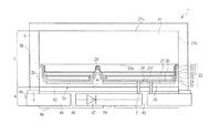
- FIG. 1 shows a schematic sectional illustration of one exemplary embodiment of an optoelectronic semiconductor component 1 described here.
- the optoelectronic semiconductor component 1 comprises an optoelectronic semiconductor chip 2 .
- the optoelectronic semiconductor chip 2 comprises a growth substrate 21 , having a growth surface 21 a , side surfaces 21 b and a bottom surface 21 c facing away from the growth surface 21 a , and also a layer sequence 22 grown on the growth surface 21 a .
- the layer sequence 22 comprises a semiconductor layer sequence 221 , 222 , 223 comprising an n-doped region 221 , which is in direct contact with the growth surface 21 a of the growth substrate 21 , an active zone 222 and a p-doped region 223 .
- the growth substrate 21 can furthermore comprise a buffer layer, wherein a top surface of the buffer layer facing away from the bottom surface 21 c forms the growth surface 21 a of the growth substrate 21 .
- the semiconductor layer sequence 221 , 222 , 223 directly adjoins the buffer layer.
- the semiconductor layer sequence, at its side facing the growth substrate 21 to comprise the buffer layer or to comprise a further buffer layer.
- the semiconductor layer sequence can comprise further layers (not shown).
- the layer sequence 22 comprises a first metallization layer 23 , an encapsulation layer 24 and a passivation layer 25 .
- the first metallization layer 23 is embodied as reflective for the electromagnetic radiation emitted by the active zone 222 .
- the first metallization layer 23 can contain silver or some other metal embodied as reflective for the electromagnetic radiation emitted by the active zone 222 .
- the encapsulation layer 24 is fitted on the side of the first metallization layer 23 facing away from the growth substrate 21 and molds over the first metallization layer 23 .
- the encapsulation layer 24 can contain platinum, gold or titanium, for example.
- the passivation layer is formed with an insulating material, such as silicon dioxide or silicon nitride, for example, and molds around the encapsulation layer 24 completely and the semiconductor layer sequence 221 , 222 , 223 at least in places.
- the encapsulation layer 24 decouples the first metallization layer 23 from the surroundings and prevents for example the penetration of air or moisture into the first metallization layer 23 . Furthermore, the encapsulation layer can suppress a migration of material from the first metallization layer 23 .
- the encapsulation layer 24 can almost completely cover the first metallization layer 23 at its top surface facing away from the semiconductor layer sequence 22 . By way of example, more than 90%, preferably more than 95%, of the top surface of the first metallization layer 23 facing away from the semiconductor layer sequence 22 can be covered by the encapsulation layer 24 , while the remaining 10%, preferably 5%, directly adjoins the passivation layer 25 .
- the optoelectronic semiconductor chip 2 comprises an insulation layer 26 and a connection carrier 4 , having a top surface 4 a and a bottom surface 4 c .
- the insulation layer 26 is arranged in places between the connection carrier 4 and the layer sequence 22 . In this case, the insulation layer 26 is in direct contact with the semiconductor layer sequence 22 at least in places.
- the insulation layer 26 can sometimes enclose the semiconductor layer sequence 221 , 222 , 223 in a framelike fashion.
- the insulation layer 26 additionally adjoins the passivation layer 25 of the optoelectronic semiconductor chip 2 .
- the insulation layer 26 adjoins the growth surface 21 a of the growth substrate 21 in places. In this case, all side surfaces 21 b and the bottom surface 21 c of the growth substrate 21 remain free of the insulation layer 26 .
- the optoelectronic semiconductor chip 2 additionally comprises contact points 29 , a second metallization layer 27 , an n-type metallization 231 and a contact layer 28 .
- the contact points are electrically conductively connected to the semiconductor layer sequence 221 , 222 , 223 of the optoelectronic semiconductor chip 2 .
- the insulation layer 26 is interrupted in places and the second metallization layer 27 penetrates through the insulation layer 26 at these locations.
- the second metallization layer 27 can be embodied such that it is electrically conductive in order to enable an electrical contacting of the contact points 29 .
- the second metallization layer 27 can be formed with titanium, silver or platinum.
- the contact points 29 can be formed for example with titanium, gold, platinum or some other electrically conductive material.
- the second metallization layer 27 is adjoined by a contact layer 28 , which can be formed with silver and/or gold, for example.
- the contact layer 28 enables a good electrical and/or mechanical connection of the optoelectronic semiconductor chip 2 to a connection carrier 4 .
- the optoelectronic semiconductor component 2 furthermore comprises the connection carrier 4 .
- the connection carrier 4 of the optoelectronic semiconductor component 1 comprises a main body 44 , a solder layer 43 , through connections 46 , an electronic component 47 and a mirror layer 6 .
- the through connections 46 penetrate through the main body 44 of the connection carrier 4 in places. Furthermore, parts of the through connections 46 cover the top surface 4 a of the connection carrier 4 at least in places. Said parts of the through connections 46 can be for example connection points and/or mounting pads with which the optoelectronic semiconductor component 1 can be mounted on a printed circuit board, for example. Said parts of the through connections 46 can consist of a different material than the rest of the through connections 46 and/or said parts can be fabricated in a separate production step.
- the through connections 46 can be electrically conductively connected to the contact points 29 . By way of example, the through connections 46 can contain copper.
- the connection carrier 4 furthermore comprises a solder layer 43 , which enables an electrical connection of the through connections 46 to the contact layer 28 , and thus to the contact points 29 .
- the solder layer 43 can be formed with gold or tin, for example. It is furthermore possible—in contrast to what is shown in the figures—for the solder layer 43 to comprise a leveling layer, which can be formed with titanium tungsten nitride, for example.
- the leveling layer serves as a diffusion barrier, for example.
- the solder layer 43 can be interrupted in places. At these locations, for example, an insulation bridge 7 can penetrate through the solder layer 43 and directly adjoin the main body 44 .
- the insulation bridge 7 can be formed with an electrically insulating material.
- the electrically insulating material can be air, for example.
- the insulation bridge 7 can accordingly be an air-filled cavity.
- the insulation bridge 7 encloses the n-type metallization layer 231 at the laterally situated outer surfaces thereof and is enclosed by the second metallization layer 27 at its laterally situated outer surfaces.
- the optoelectronic semiconductor component 1 additionally comprises a conversion layer 5 , which is applied on the bottom surface 21 c and the side surfaces 21 b of the growth substrate 21 and the side surfaces 2 b of the optoelectronic semiconductor chip that are spaced apart laterally with respect to the layer sequence 22 , and is in direct contact with these surfaces.
- the conversion layer 5 is additionally preferably in direct contact with the connection carrier 4 at least in places.
- the conversion layer 5 can be applied to the freely accessible outer surfaces of the optoelectronic semiconductor chip 2 and/or of the connection carrier 4 in a production method by means of spray coating, reshaping, electrophoresis or printing.
- the conversion layer 5 is preferably produced by a method which can be employed in the wafer assemblage and is thus cost-effective.
- the optoelectronic semiconductor component 1 can be potted in a radiation-transmissive potting body and the conversion layer 5 can be applied on the potting body in a manner spaced apart from the optoelectronic semiconductor component 1 .
- the potting body is molded around the optoelectronic semiconductor component 1 and afterward the conversion layer 5 is applied to the potting body in a manner spaced apart from the component parts of the optoelectronic semiconductor component 1 .
- the conversion layer 5 was applied to the optoelectronic semiconductor chip 2 before the optoelectronic semiconductor chip 2 was applied to the connection carrier 4 .
- the conversion layer does not adjoin the connection carrier 4 .
- the conversion layer 5 extends almost completely along the side surfaces 21 b of the growth substrate 21 and the side surfaces 2 b of the optoelectronic semiconductor chip 2 that run transversely or perpendicularly with respect to the growth surface 21 a of the growth substrate 21 , wherein a spacing remains between the conversion layer 5 and the connection carrier 4 . “Almost completely” means that, for example, at most 20%, preferably at most 10%, of the outer surfaces of the optoelectronic semiconductor chip 2 remains free of the conversion layer 5 .
- connection carrier 4 projects beyond the conversion layer 5 at the side surfaces 5 b thereof, that is to say that the side surfaces 5 b of the conversion layer 5 do not terminate flush with the side surfaces 4 b of the connection carrier 4 .
- the side surfaces 4 b of the connection carrier 4 are thus free of the conversion layer 5 .
- the side surfaces 5 b of the conversion layer 5 can have traces of singulation.
- the connection carrier 4 furthermore comprises—optionally—a mirror layer 6 , which is embodied as reflective for the electromagnetic radiation emitted by the active zone 222 of the semiconductor layer sequence 221 , 222 , 223 and the electromagnetic radiation converted by the conversion layer 5 .
- the mirror layer 6 is arranged on the main body 44 of the connection carrier 4 . Furthermore, the mirror layer 6 is arranged laterally with respect to the optoelectronic semiconductor chip 2 at least in places and directly adjoins the conversion layer 5 at least in places.
- the mirror layer 6 can enclose the optoelectronic semiconductor chip 2 in a framelike fashion, for example.
- Electromagnetic radiation which is emitted by the active zone 222 in the direction of the connection carrier 4 or is scattered in the direction of the connection carrier 4 by the scattering particles contained in the conversion element 5 is reflected back again by the mirror layer 6 in the preferred emission direction, that is to say in the direction of the growth substrate 21 .
- connection carrier 4 comprises an electronic component 47 .
- the electronic component 47 is arranged between at least two through connections 46 of the connection carrier 4 .
- the electronic component 47 is an ESD protective diode which can prevent the optoelectronic semiconductor chip from being destroyed by an electrostatic discharge, for example.
- the contacting of the electronic component 47 can be effected via at least one of the through connections 46 , for example.
- the through connections 46 also function as contactings for the optoelectronic semiconductor chip 2 . This allows a smaller number of through connections 46 and thus also a facilitated mounting and/or electrical contacting.
- the electronic component 47 can be produced for example by corresponding doping of the main body 44 .
- the doping of the main body 44 can be carried out before or after the semiconductor chip 2 is applied to the connection carrier 4 .
- FIG. 2 shows a schematic sectional illustration of a second exemplary embodiment of an optoelectronic semiconductor component 1 described here.
- the conversion element 5 directly adjoins a bottom surface 44 c of the main body 44 of the connection carrier 4 facing the optoelectronic semiconductor chip 2 . In this exemplary embodiment, therefore, no mirror layer 6 is arranged between the main body 44 and the conversion element 5 .
- connection carrier 4 moreover comprises an additional connection location 462 , with which the electronic component can be contacted independently of the optoelectronic semiconductor chip 2 .
- This configuration enables for example an electronic functional test of the electronic component 47 independently of an optoelectronic semiconductor chip 2 that has already been applied to the connection carrier 4 .
- the electronic component 47 illustrated in FIG. 2 can be an arbitrary electronic component such as, for example, a transistor, a resistor and/or an ESD protective diode.
- FIG. 3 shows a schematic sectional illustration of a third exemplary embodiment of an optoelectronic semiconductor component 1 described here.
- At least one laterally spaced apart side surface 26 b of the insulation layer 26 terminates flush with at least one side surface 21 b of the growth substrate 21 within the scope of the production tolerances.
- the conversion layer 5 may be possible for the conversion layer 5 to have a uniform thickness both in the region of the growth substrate 21 and in the region of the insulation layer 26 .
- the optoelectronic semiconductor component 1 described here can be embodied particularly compactly and in particular as a chip scale component on account of the integrated component parts, such as the conversion layer 5 and the electronic component 47 .
- the growth substrate 21 is not detached in the case of the present optoelectronic semiconductor component 1 , but rather remains at the semiconductor layer sequence 22 . This sometimes results in a significantly reduced mechanical loading of the semiconductor layers 221 , 223 grown on the growth substrate 22 .
- the optoelectronic properties of the optoelectronic semiconductor component 1 are altered to a lesser extent than in the case of an otherwise structurally identical optoelectronic semiconductor component in which the growth substrate 21 was detached. This makes it possible, in particular, to provide a compact optoelectronic semiconductor component 1 having a very narrow distribution of the optoelectronic properties.
Landscapes
- Engineering & Computer Science (AREA)
- Microelectronics & Electronic Packaging (AREA)
- Computer Hardware Design (AREA)
- Power Engineering (AREA)
- Manufacturing & Machinery (AREA)
- Physics & Mathematics (AREA)
- Condensed Matter Physics & Semiconductors (AREA)
- General Physics & Mathematics (AREA)
- Led Device Packages (AREA)
Applications Claiming Priority (4)
| Application Number | Priority Date | Filing Date | Title |
|---|---|---|---|
| DE102014101492 | 2014-02-06 | ||
| DE102014101492.8A DE102014101492A1 (de) | 2014-02-06 | 2014-02-06 | Optoelektronisches Halbleiterbauelement |
| DE102014101492.8 | 2014-02-06 | ||
| PCT/EP2015/051148 WO2015117824A1 (fr) | 2014-02-06 | 2015-01-21 | Composant optoélectronique à semi-conducteur |
Publications (2)
| Publication Number | Publication Date |
|---|---|
| US20160351758A1 US20160351758A1 (en) | 2016-12-01 |
| US9780265B2 true US9780265B2 (en) | 2017-10-03 |
Family
ID=52355002
Family Applications (1)
| Application Number | Title | Priority Date | Filing Date |
|---|---|---|---|
| US15/117,177 Active US9780265B2 (en) | 2014-02-06 | 2015-01-21 | Optoelectronic semiconductor component |
Country Status (3)
| Country | Link |
|---|---|
| US (1) | US9780265B2 (fr) |
| DE (2) | DE102014101492A1 (fr) |
| WO (1) | WO2015117824A1 (fr) |
Cited By (2)
| Publication number | Priority date | Publication date | Assignee | Title |
|---|---|---|---|---|
| US10243117B2 (en) | 2015-05-13 | 2019-03-26 | Osram Opto Semiconductors Gmbh | Method for producing optoelectronic devices and surface-mountable optoelectronic device |
| US11069842B2 (en) | 2017-04-04 | 2021-07-20 | Osram Oled Gmbh | Method for producing an optoelectronic semiconductor component and optoelectronic semiconductor component |
Families Citing this family (8)
| Publication number | Priority date | Publication date | Assignee | Title |
|---|---|---|---|---|
| DE102016106928A1 (de) | 2016-04-14 | 2017-10-19 | Osram Opto Semiconductors Gmbh | Optoelektronischer Halbleiterchip und Verfahren zur Herstellung eines optoelektronischen Halbleiterchips |
| DE102017105235B4 (de) * | 2017-03-13 | 2022-06-02 | OSRAM Opto Semiconductors Gesellschaft mit beschränkter Haftung | Bauelement mit Verstärkungsschicht und Verfahren zur Herstellung eines Bauelements |
| DE102017123242A1 (de) * | 2017-10-06 | 2019-04-11 | Osram Opto Semiconductors Gmbh | Verfahren zur Herstellung eines oder einer Mehrzahl von Halbleiterchips und Halbleiterchip |
| DE102017125105A1 (de) * | 2017-10-26 | 2019-05-02 | Osram Opto Semiconductors Gmbh | Optoelektronischer Halbleiterchip |
| FR3077160B1 (fr) | 2018-01-19 | 2022-01-21 | Commissariat Energie Atomique | Dispositif optoelectronique comportant une grille et une cathode couplees l'une a l'autre |
| DE102020104372A1 (de) * | 2020-01-15 | 2021-07-15 | OSRAM Opto Semiconductors Gesellschaft mit beschränkter Haftung | Optoelektronischer Halbleiterchip |
| DE102020116871A1 (de) | 2020-06-26 | 2021-12-30 | OSRAM Opto Semiconductors Gesellschaft mit beschränkter Haftung | Optoelektronischer halbleiterchip |
| DE102021202026A1 (de) | 2021-03-03 | 2022-09-08 | OSRAM Opto Semiconductors Gesellschaft mit beschränkter Haftung | Optoelektronisches halbleiterbauelement und verfahren zur herstellung zumindest eines optoelektronischen halbleiterbauelements |
Citations (16)
| Publication number | Priority date | Publication date | Assignee | Title |
|---|---|---|---|---|
| DE102005007601A1 (de) | 2004-02-20 | 2005-09-08 | Osram Opto Semiconductors Gmbh | Optoelektronisches Bauelement, Vorrichtung mit einer Mehrzahl optoelektronischer Bauelemente und Verfahren zur Herstellung eines optoelektronischen Bauelements |
| DE102008010512A1 (de) | 2008-02-22 | 2009-08-27 | Osram Opto Semiconductors Gmbh | Optoelektronisches Bauteil und Verfahren zur Herstellung eines optoelektronischen Bauteils |
| DE102009022966A1 (de) | 2009-05-28 | 2010-12-02 | Osram Opto Semiconductors Gmbh | Oberflächenmontierbarer optoelektronischer Halbleiterchip und Verfahren zur Herstellung eines oberflächenmontierbaren optoelektronischen Halbleiterchips |
| DE102009032486A1 (de) | 2009-07-09 | 2011-01-13 | Osram Opto Semiconductors Gmbh | Optoelektronisches Bauelement |
| DE102009051746A1 (de) | 2009-09-30 | 2011-03-31 | Osram Opto Semiconductors Gmbh | Optoelektronisches Bauelement |
| DE102010025320A1 (de) | 2010-06-28 | 2011-12-29 | Osram Opto Semiconductors Gmbh | Optoelektronisches Bauelement und Verfahren zu dessen Herstellung |
| DE102011011378A1 (de) | 2011-02-16 | 2012-08-16 | Osram Opto Semiconductors Gmbh | Trägersubstrat und Verfahren zur Herstellung von Halbleiterchips |
| EP2503606A2 (fr) | 2011-03-25 | 2012-09-26 | Samsung LED Co., Ltd. | Diode électroluminescente, procédé de fabrication de celui-ci, module à plusieurs diodes électroluminescentes, et procédé de fabrication de celui-ci |
| US20120241793A1 (en) | 2011-03-22 | 2012-09-27 | Seoul Opto Device Co., Ltd. | Light emitting diode package and method for manufacturing the same |
| DE102011015821A1 (de) | 2011-04-01 | 2012-10-04 | Osram Opto Semiconductors Gmbh | Optoelektronischer Halbleiterchip |
| WO2012152307A1 (fr) | 2011-05-06 | 2012-11-15 | Osram Opto Semiconductors Gmbh | Ensemble support de composants comprenant une structure de tranchées séparant les zones de support de composants et procédé de fabrication d'une pluralité de zones de support de composants |
| WO2014006539A1 (fr) | 2012-07-05 | 2014-01-09 | Koninklijke Philips N.V. | Phosphore séparé d'une led par un matériau tampon transparent |
| WO2014040993A1 (fr) | 2012-09-14 | 2014-03-20 | Osram Opto Semiconductors Gmbh | Dispositif à semi-conducteur optoélectronique et ensemble support |
| WO2014048997A1 (fr) | 2012-09-28 | 2014-04-03 | Osram Opto Semiconductors Gmbh | Procédé de fabrication d'un composant optoélectronique |
| US20150207046A1 (en) * | 2013-12-06 | 2015-07-23 | Nichia Corporation | Light emitting device and method of manufacturing light emitting device |
| US20160240735A1 (en) * | 2013-04-11 | 2016-08-18 | Koninklijke Philips N.V. | Top emitting semiconductor light emitting device |
-
2014
- 2014-02-06 DE DE102014101492.8A patent/DE102014101492A1/de not_active Withdrawn
-
2015
- 2015-01-21 WO PCT/EP2015/051148 patent/WO2015117824A1/fr active Application Filing
- 2015-01-21 DE DE112015000703.2T patent/DE112015000703B4/de active Active
- 2015-01-21 US US15/117,177 patent/US9780265B2/en active Active
Patent Citations (17)
| Publication number | Priority date | Publication date | Assignee | Title |
|---|---|---|---|---|
| DE102005007601A1 (de) | 2004-02-20 | 2005-09-08 | Osram Opto Semiconductors Gmbh | Optoelektronisches Bauelement, Vorrichtung mit einer Mehrzahl optoelektronischer Bauelemente und Verfahren zur Herstellung eines optoelektronischen Bauelements |
| DE102008010512A1 (de) | 2008-02-22 | 2009-08-27 | Osram Opto Semiconductors Gmbh | Optoelektronisches Bauteil und Verfahren zur Herstellung eines optoelektronischen Bauteils |
| DE102009022966A1 (de) | 2009-05-28 | 2010-12-02 | Osram Opto Semiconductors Gmbh | Oberflächenmontierbarer optoelektronischer Halbleiterchip und Verfahren zur Herstellung eines oberflächenmontierbaren optoelektronischen Halbleiterchips |
| DE102009032486A1 (de) | 2009-07-09 | 2011-01-13 | Osram Opto Semiconductors Gmbh | Optoelektronisches Bauelement |
| DE102009051746A1 (de) | 2009-09-30 | 2011-03-31 | Osram Opto Semiconductors Gmbh | Optoelektronisches Bauelement |
| WO2011039023A1 (fr) | 2009-09-30 | 2011-04-07 | Osram Opto Semiconductors Gmbh | Composant optoélectronique |
| DE102010025320A1 (de) | 2010-06-28 | 2011-12-29 | Osram Opto Semiconductors Gmbh | Optoelektronisches Bauelement und Verfahren zu dessen Herstellung |
| DE102011011378A1 (de) | 2011-02-16 | 2012-08-16 | Osram Opto Semiconductors Gmbh | Trägersubstrat und Verfahren zur Herstellung von Halbleiterchips |
| US20120241793A1 (en) | 2011-03-22 | 2012-09-27 | Seoul Opto Device Co., Ltd. | Light emitting diode package and method for manufacturing the same |
| EP2503606A2 (fr) | 2011-03-25 | 2012-09-26 | Samsung LED Co., Ltd. | Diode électroluminescente, procédé de fabrication de celui-ci, module à plusieurs diodes électroluminescentes, et procédé de fabrication de celui-ci |
| DE102011015821A1 (de) | 2011-04-01 | 2012-10-04 | Osram Opto Semiconductors Gmbh | Optoelektronischer Halbleiterchip |
| WO2012152307A1 (fr) | 2011-05-06 | 2012-11-15 | Osram Opto Semiconductors Gmbh | Ensemble support de composants comprenant une structure de tranchées séparant les zones de support de composants et procédé de fabrication d'une pluralité de zones de support de composants |
| WO2014006539A1 (fr) | 2012-07-05 | 2014-01-09 | Koninklijke Philips N.V. | Phosphore séparé d'une led par un matériau tampon transparent |
| WO2014040993A1 (fr) | 2012-09-14 | 2014-03-20 | Osram Opto Semiconductors Gmbh | Dispositif à semi-conducteur optoélectronique et ensemble support |
| WO2014048997A1 (fr) | 2012-09-28 | 2014-04-03 | Osram Opto Semiconductors Gmbh | Procédé de fabrication d'un composant optoélectronique |
| US20160240735A1 (en) * | 2013-04-11 | 2016-08-18 | Koninklijke Philips N.V. | Top emitting semiconductor light emitting device |
| US20150207046A1 (en) * | 2013-12-06 | 2015-07-23 | Nichia Corporation | Light emitting device and method of manufacturing light emitting device |
Cited By (2)
| Publication number | Priority date | Publication date | Assignee | Title |
|---|---|---|---|---|
| US10243117B2 (en) | 2015-05-13 | 2019-03-26 | Osram Opto Semiconductors Gmbh | Method for producing optoelectronic devices and surface-mountable optoelectronic device |
| US11069842B2 (en) | 2017-04-04 | 2021-07-20 | Osram Oled Gmbh | Method for producing an optoelectronic semiconductor component and optoelectronic semiconductor component |
Also Published As
| Publication number | Publication date |
|---|---|
| US20160351758A1 (en) | 2016-12-01 |
| WO2015117824A1 (fr) | 2015-08-13 |
| DE112015000703B4 (de) | 2021-07-01 |
| DE112015000703A5 (de) | 2016-10-20 |
| DE102014101492A1 (de) | 2015-08-06 |
Similar Documents
| Publication | Publication Date | Title |
|---|---|---|
| US9780265B2 (en) | Optoelectronic semiconductor component | |
| TWI682558B (zh) | 半導體發光裝置 | |
| KR20160113042A (ko) | 발광 다이오드를 포함하는 광전자 디바이스 | |
| US8878205B2 (en) | Light emitting diode wafer-level package with self-aligning features | |
| CN107924974B (zh) | 光电子半导体器件及其制造方法 | |
| US8853732B2 (en) | Optoelectronic component | |
| US9583681B2 (en) | Light emitter device packages, modules and methods | |
| US9653670B2 (en) | Method for producing an optoelectronic semiconductor component, and optoelectronic semiconductor component | |
| US9293663B1 (en) | Light-emitting unit and semiconductor light-emitting device | |
| KR101590235B1 (ko) | 광전자 반도체 칩 | |
| KR20150056559A (ko) | 서로 나란히 배치되는 복수의 활성 영역을 포함한 광전자 반도체 칩 | |
| US10651337B2 (en) | Supporting substrate for semiconductor device, semiconductor apparatus comprising the same, and method for manufacturing the same | |
| US8754440B2 (en) | Light-emitting diode (LED) package systems and methods of making the same | |
| US20180090652A1 (en) | Optoelectronic device array and method for producing a multiplicity of optoelectronic device arrays | |
| TW201409767A (zh) | 藉由透明分隔物與發光二極體隔開之磷光體 | |
| US10727373B2 (en) | Light emitting diode, method for manufacturing light emitting diode, light emitting diode display device, and method for manufacturing light emitting diode display device | |
| US9012951B2 (en) | Radiation-emitting component and method for producing a radiation-emitting component | |
| EP2427923B1 (fr) | Extension de plots de connexion jusqu'au bord de la puce avec isolation électrique | |
| WO2017154975A1 (fr) | Dispositif électroluminescent à semi-conducteurs | |
| US10312285B2 (en) | LED illuminator and method of making the same | |
| KR101863129B1 (ko) | 광전자 반도체 소자의 제조 방법, 및 광전자 반도체 소자 | |
| KR20180025833A (ko) | Uv led 패키지 | |
| US20190140145A1 (en) | Light-Emitting Device and Method for Manufacturing a Light-Emitting Device | |
| US20150280084A1 (en) | Semiconductor light emitting device and method of manufacturing same | |
| US20150303179A1 (en) | Light Emitting Diode Assembly With Integrated Circuit Element |
Legal Events
| Date | Code | Title | Description |
|---|---|---|---|
| AS | Assignment |
Owner name: OSRAM OPTO SEMICONDUCTORS GMBH, GERMANY Free format text: ASSIGNMENT OF ASSIGNORS INTEREST;ASSIGNORS:HERRMANN, SIEGFRIED;MOOSBURGER, JUEERGEN;ILLEK, STEFAN;AND OTHERS;SIGNING DATES FROM 20160915 TO 20161016;REEL/FRAME:041209/0114 |
|
| STCF | Information on status: patent grant |
Free format text: PATENTED CASE |
|
| AS | Assignment |
Owner name: OSRAM OLED GMBH, GERMANY Free format text: ASSIGNMENT OF ASSIGNORS INTEREST;ASSIGNOR:OSRAM OPTO SEMICONDUCTORS GMBH;REEL/FRAME:051467/0906 Effective date: 20191218 |
|
| MAFP | Maintenance fee payment |
Free format text: PAYMENT OF MAINTENANCE FEE, 4TH YEAR, LARGE ENTITY (ORIGINAL EVENT CODE: M1551); ENTITY STATUS OF PATENT OWNER: LARGE ENTITY Year of fee payment: 4 |