US9723236B2 - Photoelectric conversion apparatus and method for driving photoelectric conversion apparatus - Google Patents
Photoelectric conversion apparatus and method for driving photoelectric conversion apparatus Download PDFInfo
- Publication number
- US9723236B2 US9723236B2 US14/819,085 US201514819085A US9723236B2 US 9723236 B2 US9723236 B2 US 9723236B2 US 201514819085 A US201514819085 A US 201514819085A US 9723236 B2 US9723236 B2 US 9723236B2
- Authority
- US
- United States
- Prior art keywords
- signal
- photoelectric conversion
- pixels
- electrode
- relationship
- Prior art date
- Legal status (The legal status is an assumption and is not a legal conclusion. Google has not performed a legal analysis and makes no representation as to the accuracy of the status listed.)
- Expired - Fee Related
Links
Images


Classifications
-
- H04N5/3745—
-
- H—ELECTRICITY
- H04—ELECTRIC COMMUNICATION TECHNIQUE
- H04N—PICTORIAL COMMUNICATION, e.g. TELEVISION
- H04N25/00—Circuitry of solid-state image sensors [SSIS]; Control thereof
- H04N25/70—SSIS architectures; Circuits associated therewith
- H04N25/76—Addressed sensors, e.g. MOS or CMOS sensors
- H04N25/77—Pixel circuitry, e.g. memories, A/D converters, pixel amplifiers, shared circuits or shared components
-
- H01L27/14643—
-
- H—ELECTRICITY
- H10—SEMICONDUCTOR DEVICES; ELECTRIC SOLID-STATE DEVICES NOT OTHERWISE PROVIDED FOR
- H10F—INORGANIC SEMICONDUCTOR DEVICES SENSITIVE TO INFRARED RADIATION, LIGHT, ELECTROMAGNETIC RADIATION OF SHORTER WAVELENGTH OR CORPUSCULAR RADIATION
- H10F39/00—Integrated devices, or assemblies of multiple devices, comprising at least one element covered by group H10F30/00, e.g. radiation detectors comprising photodiode arrays
- H10F39/10—Integrated devices
- H10F39/12—Image sensors
- H10F39/18—Complementary metal-oxide-semiconductor [CMOS] image sensors; Photodiode array image sensors
-
- H01L27/307—
-
- H—ELECTRICITY
- H10—SEMICONDUCTOR DEVICES; ELECTRIC SOLID-STATE DEVICES NOT OTHERWISE PROVIDED FOR
- H10K—ORGANIC ELECTRIC SOLID-STATE DEVICES
- H10K39/00—Integrated devices, or assemblies of multiple devices, comprising at least one organic radiation-sensitive element covered by group H10K30/00
- H10K39/30—Devices controlled by radiation
- H10K39/32—Organic image sensors
Definitions
- the present invention relates to a photoelectric conversion apparatus and a method for driving a photoelectric conversion apparatus.
- Japanese Patent Laid-Open No. 8-116044 discloses a Metal Insulator Semiconductor-type photoelectric conversion unit including a first electrode, a second electrode, and a photoelectric conversion layer between the first electrode and the second electrode.
- Japanese Patent Laid-Open No. 8-116044 discloses that, in order to discharge signal charges stored in the photoelectric conversion layer, the potential magnitude relationship between the first electrode and the second electrode is reversed from that at the time of the storage of signal charges and is then reversed again to that at the time of the storage of signal charges.
- Japanese Patent Laid-Open No. 8-116044 discloses that, in order to reverse the potential magnitude relationship between the first electrode and the second electrode at the time of the storage and discharge of signal charges, a potential different from that supplied at the time of the storage of signal charges is supplied to the first electrode or the second electrode at the time of the discharge of signal charges.
- a potential supplied to the first electrode or the second electrode is changed in a plurality of pixels at the same time, a large current passes through a supply line connected to the first electrodes or the second electrodes whose potentials have been changed and the potential of the supply line is changed. Because of this change in the potential of the supply line, the amount of discharge of signal charges varies from pixel to pixel.
- the present invention provides a technique for suppressing the effect of a voltage drop at a supply line caused by the change in an inter-electrode voltage.
- a photoelectric conversion apparatus includes a plurality of pixels each including a photoelectric conversion unit and a pixel output unit.
- the photoelectric conversion unit includes a first electrode, a second electrode, a photoelectric conversion layer that is disposed between the first electrode and the second electrode and is configured to store signal charges, and an insulating layer disposed between the photoelectric conversion layer and the second electrode.
- An optical signal based on the signal charges stored by the photoelectric conversion unit is output to an input node of the pixel output unit.
- a method for driving a photoelectric conversion apparatus including a plurality of pixels each including a photoelectric conversion unit and a pixel output unit.
- the photoelectric conversion unit includes a first electrode, a second electrode, a photoelectric conversion layer that is disposed between the first electrode and the second electrode and is configured to store signal charges, and an insulating layer disposed between the photoelectric conversion layer and the second electrode.
- the method includes outputting an optical signal based on the signal charges stored by the photoelectric conversion unit to an input node of the pixel output unit and making an overlap between a time at which a potential magnitude relationship between the first electrode and the second electrode is changed from a first relationship in which a potential of the first electrode is lower than that of the second electrode to a second relationship opposite to the first relationship in a part of the plurality of pixels and a time at which a potential magnitude relationship between the first electrode and the second electrode is changed from the second relationship to the first relationship in the other part of the plurality of pixels.
- FIG. 1 is a diagram illustrating an exemplary configuration of a photoelectric conversion apparatus.
- FIG. 2A is a diagram illustrating an exemplary configuration of a pixel.
- FIG. 2B is a diagram illustrating an exemplary configuration of a pixel processing unit.
- FIG. 3 is a diagram illustrating an exemplary operation of a photoelectric conversion apparatus.
- FIG. 4A is a diagram illustrating another exemplary configuration of a pixel.
- FIG. 4B is a diagram illustrating another exemplary configuration of a pixel.
- FIGS. 5A to 5D are diagrams illustrating an exemplary operation of a photoelectric conversion unit.
- FIG. 6 is a diagram illustrating another exemplary operation of a photoelectric conversion apparatus.
- FIG. 7 is a diagram illustrating another exemplary operation of a photoelectric conversion apparatus.
- FIG. 8 is a diagram illustrating another exemplary operation of a photoelectric conversion apparatus.
- FIG. 9A is a diagram illustrating another exemplary configuration of a pixel processing unit.
- FIG. 9B is a diagram illustrating another exemplary configuration of a pixel processing unit.
- FIG. 10 is a diagram illustrating another exemplary configuration of a photoelectric conversion apparatus.
- FIG. 11 is a diagram illustrating an exemplary configuration of a photoelectric conversion system.
- FIG. 1 is a diagram illustrating the configuration of a photoelectric conversion apparatus according to the first embodiment.
- a photoelectric conversion apparatus 1 includes a plurality of pixel rows 2 of pixels 10 .
- the pixels 10 are arranged in a matrix.
- the photoelectric conversion apparatus 1 further includes a vertical scanning circuit 3 , a driving signal supply unit 4 , a plurality of switch units 5 corresponding to the pixel rows 2 , a timing generator (hereinafter referred to as TG) 6 , a signal processing unit 7 , and a plurality of vertical signal lines 17 corresponding to a plurality of columns of the pixels 10 .
- TG timing generator
- the driving signal supply unit 4 outputs a control signal to each of the switch units 5 .
- the switch units 5 correspond one-to-one to the pixel rows 2 .
- the signal processing unit 7 is illustrated in the form of a single block, but includes a plurality of column signal processing circuits corresponding one-to-one to the columns of the pixels 10 .
- a first pixel row V 1 , a fourth pixel row V 4 , and a seventh pixel row V 7 , which are illustrated in FIG. 1 belong to a first group.
- a second pixel row, a fifth pixel row, and an eighth pixel row belong to a second group.
- a third pixel row, a sixth pixel row, and a ninth pixel row belong to a third group.
- a common signal is supplied from the driving signal supply unit 4 to the pixel rows in the same group.
- FIG. 2A illustrates one of the pixels 10 illustrated in FIG. 1 .
- the pixel 10 includes a photodiode PD, a transfer transistor 13 , a reset transistor 14 , a first pixel output unit 16 , a pixel current source 18 , and a pixel processing unit 20 .
- the first pixel output unit 16 includes a first amplification transistor 16 a and a first selection transistor 16 b.
- a signal ⁇ T transmitted from the switch unit 5 illustrated in FIG. 1 is input into a control node of the transfer transistor 13 .
- a signal ⁇ Res transmitted from the switch unit 5 illustrated in FIG. 1 is input into a control node of the reset transistor 14 .
- a voltage Vd 1 is input into one of main nodes of the reset transistor 14 .
- a signal ⁇ Sel transmitted from the switch unit 5 illustrated in FIG. 1 is input into a control node of the first selection transistor 16 b.
- a voltage Vd 2 is input into one of main nodes of the first amplification transistor 16 a .
- the first amplification transistor 16 a and the pixel current source 18 form a source follower circuit.
- Each of the transfer transistor 13 , the reset transistor 14 , and the first selection transistor 16 b is a switch for switching between a conductive state and a nonconductive state in accordance with the signal level of a signal input into a control node.
- FIG. 2B is a diagram illustrating the configuration of the pixel processing unit 20 illustrated in FIG. 2A .
- the pixel processing unit 20 includes transistors 21 , 22 , 23 , and 24 , a second pixel output unit 25 , and capacitative elements CN and CS.
- the second pixel output unit 25 includes a second amplification transistor 25 a and a second selection transistor 25 b .
- a voltage Vd 2 is input into one of main nodes of the second amplification transistor 25 a .
- the second amplification transistor 25 a and a current source 30 for supplying a current to the vertical signal lines 17 form a source follower circuit.
- a node A is on an electric path between the first selection transistor 16 b and the transistor 21 .
- a signal ⁇ TNS transmitted from the switch unit 5 is input into a control node of the transistor 21 .
- a signal ⁇ TN transmitted from the switch unit 5 is input into a control node of the transistor 22 .
- a signal ⁇ TS transmitted from the switch unit 5 is input into a control node of the transistor 23 .
- a signal ⁇ TC transmitted from the switch unit 5 is input into a control node of the transistor 24 .
- a voltage Vrf 1 is input into one of main nodes of the transistor 24 .
- a signal ⁇ Sel 2 transmitted from the switch unit 5 is input into one of main nodes of the second selection transistor 25 b.
- FIG. 3 is a timing diagram illustrating the operation of the photoelectric conversion apparatus illustrated in FIG. 1 .
- Signals ⁇ Res 1 and ⁇ T 1 illustrated in FIG. 3 are supplied to the pixels 10 in the first group and correspond to the signals ⁇ Res and ⁇ T illustrated in FIG. 2A , respectively.
- Signals ⁇ TN 1 and ⁇ TS 1 illustrated in FIG. 3 are supplied to the pixels 10 in the first group and correspond to the signals ⁇ TN and ⁇ TS illustrated in FIG. 2B , respectively.
- Signals ⁇ Res 2 and ⁇ T 2 illustrated in FIG. 3 are supplied to the pixels 10 in the second group and correspond to the signals ⁇ Res and ⁇ T illustrated in FIG. 2A , respectively.
- Signals ⁇ TN 2 and ⁇ TS 2 illustrated in FIG. 3 are supplied to the pixels 10 in the second group and correspond to the signals ⁇ TN and ⁇ TS illustrated in FIG. 2B , respectively.
- Signals ⁇ Sel and ⁇ TNS are common signals supplied to all rows of the pixels 10 illustrated in FIG. 1 .
- Signals ⁇ Sel 2 , ⁇ TC, ⁇ TN, and ⁇ TS are supplied to each row of the pixels 10 .
- the driving signal supply unit 4 sequentially changes the signal levels of the signals ⁇ Res 1 , ⁇ Res 2 , and ⁇ Res 3 , which are to be transmitted to corresponding groups of the pixels 10 , from Lo to Hi. Furthermore, the driving signal supply unit 4 sequentially changes the signal levels of the signals ⁇ T 1 , ⁇ T 2 , and ⁇ T 3 , which are to be transmitted to corresponding groups of the pixels 10 , from Lo to Hi.
- the operation illustrated in FIG. 3 reduces the difference in exposure timing between rows of the pixels 10 .
- the operation illustrated in FIG. 3 can be regarded as a pseudo-global shutter.
- a period TA includes periods TRes and TTS.
- the driving signal supply unit 4 sequentially changes the signal levels of the signals ⁇ Res 1 , ⁇ Res 2 , and ⁇ Res 3 from Lo to Hi.
- the potentials of nodes FD of the pixels 10 in the first group, the second group, and the third group are reset in accordance with the voltage Vd 1 .
- the driving signal supply unit 4 sequentially changes the signal levels of the signals ⁇ TN 1 , ⁇ TN 2 , and ⁇ TN 3 from Lo to Hi.
- the capacitative element CN stores a signal that is output from the first amplification transistor 16 a after the reset of the node FD has been canceled.
- the signal output from the first amplification transistor 16 a and the signal stored in the capacitative element CN are denoted as noise signals.
- a period in which the driving signal supply unit 4 sets the signal level of the signal ⁇ Res 1 to Hi and a period in which the driving signal supply unit 4 sets the signal level of the signal ⁇ TN 1 to Hi partially overlap. That is, in a photoelectric conversion apparatus according to this embodiment, the pixel processing unit 20 samples a noise signal in a period in which the node FD is reset. As compared with a configuration in which the pixel processing unit 20 starts to sample a noise signal after the reset of the node FD has been completed, the dark current component of the node FD included in a noise signal can be reduced with this configuration.
- the driving signal supply unit 4 sequentially sets the signal levels of the signals ⁇ TN 1 , ⁇ TN 2 , and ⁇ TN 3 to Hi. As a result, the output of a noise signal to the capacitative element CN is sequentially performed in the three groups of the pixels 10 .
- the signal level of the signal ⁇ Res 1 is changed from Hi to Lo and the signal level of the signal ⁇ Res 2 is changed from Lo to Hi.
- the signal level of the signal ⁇ Res 2 is changed from Hi to Lo and the signal level of the signal ⁇ Res 3 is changed from Lo to Hi.
- the driving signal supply unit 4 sequentially changes the signal levels of the signals ⁇ T 1 , ⁇ T 2 , and ⁇ T 3 from Lo to Hi.
- the node FD in each pixel 10 in all rows has a potential based on charges transmitted from the photodiode PD.
- the driving signal supply unit 4 sequentially changes the signal levels of the signals ⁇ TS 1 , ⁇ TS 2 , and ⁇ TS 3 from Lo to Hi.
- the capacitative element CS stores a signal output from the first amplification transistor 16 a in accordance with the potential of the node FD based on the charges transferred from the photodiode PD.
- the signal output from the first amplification transistor 16 a and the signal stored by the capacitative element CS are denoted as optical signals.
- the pixel processing unit 20 samples an optical signal in a period in which charges are transferred from the photodiode PD to the node FD.
- the dark current component of the node FD included in the optical signal can be reduced with this configuration.
- a noise signal and an optical signal are output from each row of the pixel 10 and input into a corresponding column signal processing circuit in the signal processing unit 7 via the vertical signal line 17 .
- the column signal processing circuit externally outputs from a photoelectric conversion apparatus according to this embodiment a signal obtained by subtracting the noise signal from the optical signal.
- the photoelectric conversion apparatus can output a signal whose signal-to-noise ratio is better than that of an optical signal.
- the capacitative element CN in each pixel 10 in the first row stores a noise signal.
- the capacitative element CS in each pixel 10 in the first row stores an optical signal.
- the vertical scanning circuit 3 sets the signal level of the signal ⁇ Sel 2 - n to Hi, so that the second selection transistor 25 b in each pixel 10 in the first row is turned on. This allows the second pixel output unit 25 to output a signal to the corresponding vertical signal line 17 .
- the vertical scanning circuit 3 sets the signal level of the signal ⁇ TC-n to Hi, so that the transistor 24 is turned on. As a result, the potential of a node B that is the gate of the second amplification transistor 25 a is reset to the potential of the voltage Vrf 1 .
- the vertical scanning circuit 3 sets the signal level of the signal ⁇ TN-n to hi, so that the transistor 22 is turned on. As a result, a noise signal is input into a column signal processing circuit via the second pixel output unit 25 and the vertical signal line 17 . Subsequently, the vertical scanning circuit 3 sets the signal level of the signal ⁇ TC-n to Hi again, so that the potential of the node B is reset. Subsequently, the vertical scanning circuit 3 sets the signal level of the signal ⁇ TS-n to Hi, so that the transistor 23 is turned on. As a result, an optical signal is output to the column signal processing circuit via the second pixel output unit 25 and the vertical signal line 17 .
- a photoelectric conversion apparatus performs this operation of the period TV 1 for each row of the pixels 10 .
- the pixels 10 in each row sequentially outputs optical signals and noise signals to the column signal processing circuit.
- the pixel processing unit 20 samples a noise signal while the node FD is reset.
- the dark current component of the node FD included in a noise signal can therefore be reduced.
- a photoelectric conversion apparatus according to this embodiment has the following effect.
- the pixels 10 are divided into a plurality of groups and a time at which the signal level of a driving signal is changed varies from group to group.
- the signal ⁇ Res which is one of driving signals
- the nodes FD in the pixels 10 in all rows are electrically connected to the corresponding power sources Vd 1 at the same time.
- a current flows between the node FD and the power source Vd 1 in the pixels 10 in all rows at the same time, so that the potential of the power source Vd 1 is changed.
- This change in the potential of the power source Vd 1 temporarily changes the potential of the node FD after the reset.
- the temporary change in the potential of the node FD changes the potential of a noise signal stored in the capacitative element CN.
- the first amplification transistor 16 a outputs an optical signal in a state where the temporary change in the potential of the node FD is reduced as compared with a period in which the first amplification transistor 16 a outputs a noise signal.
- the signal level of a noise component included in a noise signal and the signal level of a noise component included in an optical signal therefore differ from each other.
- the column signal processing circuit cannot accurately subtract the noise signal from the optical signal.
- the time at which the signal level of the signal ⁇ Res, which is one of driving signals, is changed from Lo to hi varies from group to group.
- the pixels 10 in all rows are subjected to the reset of the potential of the node FD in units of groups, and are therefore electrically connected to the corresponding power sources Vd 1 in units of groups. Accordingly, as compared with a case where the pixels 10 in all rows are electrically connected to the corresponding power sources Vd 1 at the same time, the amount of change in the potential of the power source Vd 1 can be reduced in a photoelectric conversion apparatus according to this embodiment. That is, the amount of change in the potential of a noise signal can be reduced, the signal level of a noise component included in an optical signal and the signal level of a noise component included in a noise signal can be easily made to conform to each other, and the column signal processing circuit can output a signal obtained by accurately subtracting the noise signal from the optical signal.
- the pixels 10 are divided into three groups.
- the number of groups is not limited, and may be from two to X inclusive assuming that the number of the pixels 10 is X.
- the column signal processing circuit in the signal processing unit 7 obtains the difference between an optical signal and a noise signal.
- the photoelectric conversion apparatus may externally output the noise signal and the optical signal and the difference between them may be obtained outside the photoelectric conversion apparatus.
- the signal processing unit 7 includes an output unit for externally outputting signals sequentially output from a plurality of column signal processing circuits
- the output unit may obtain the difference between an optical signal and a noise signal.
- the column signal processing circuit may include a clamp capacitor for storing a noise signal. In this case, an optical signal is output to a circuit at a subsequent stage via the clamp capacitor storing a noise signal. A signal of the difference between the optical signal and the noise signal is output to the circuit subsequent to the clamp capacitor.
- the configuration of the pixel processing unit 20 according to this embodiment is not limited to the configuration illustrated in FIG. 2B . Other configurations of the pixel processing unit 20 will be described.
- FIGS. 9A and 9B are diagrams illustrating the configurations of the pixel processing unit 20 . Referring to FIGS. 9A and 9B , the same reference numerals are used to identify parts already described with reference to FIG. 2B .
- the pixel processing unit 20 illustrated in FIG. 9A will be described.
- the capacitative element CN is electrically connected to an electric path between a transistor 21 N and a transistor 22 N.
- the capacitative element CS is electrically connected to an electric path between a transistor 21 S and a transistor 22 S.
- the transistors 21 N and 21 S are electrically connected to the same node A.
- the transistors 22 N and 22 S are electrically connected to the same node B.
- Signals ⁇ TNW, ⁇ TNR, ⁇ TSW, and ⁇ TSR are supplied from the driving signal supply unit 4 to the gates of the transistors 21 N, 22 N, 21 S, and 22 S, respectively.
- the waveform of the signal ⁇ TNW for the pixels 10 in the first group is the same as that of the signal ⁇ TN 1 illustrated in FIG. 3 .
- the waveform of the signal ⁇ TNW for the pixels 10 in the second group is the same as that of the signal ⁇ TN 2 illustrated in FIG. 3 .
- the waveform of the signal ⁇ TNW for the pixels 10 in the third group is the same as that of the signal ⁇ TN 3 illustrated in FIG. 3 .
- the waveform of the signal ⁇ TSW for the pixels 10 in the first group is the same as that of the signal ⁇ TS 1 illustrated in FIG. 3 .
- the waveform of the signal ⁇ TSW for the pixels 10 in the second group is the same as that of the signal ⁇ TS 2 illustrated in FIG. 3 .
- the waveform of the signal ⁇ TSW for the pixels 10 in the third group is the same as that of the signal ⁇ TS 3 illustrated in FIG. 3 .
- the waveform of the signal ⁇ TNR for the pixels 10 in the nth row is the same as that of the signal ⁇ TN-n illustrated in FIG. 3 .
- the waveform of the signal ⁇ TNR for the pixels 10 in the (n+1)th row is the same as that of the signal ⁇ TN-n+1 illustrated in FIG. 3 .
- the waveform of the signal ⁇ TSR for the pixels 10 in the nth row is the same as that of the signal ⁇ TS-n illustrated in FIG. 3 .
- the waveform of the signal ⁇ TSR for the pixels 10 in the (n+1)th row is the same as that of the signal ⁇ TS-n+1 illustrated in FIG. 3 .
- the pixel processing unit 20 illustrated in FIG. 9A can output a noise signal and an optical signal to the vertical signal line 17 .
- a capacitative element CL clamps a noise signal.
- the pixel processing unit 20 includes a third pixel output unit 25 - 1 and a fourth pixel output unit 25 - 2 .
- the third pixel output unit 25 - 1 includes a third amplification transistor 250 a and a third selection transistor 250 b .
- the input node of the third amplification transistor 250 a is electrically connected to the capacitative element CS and the transistor 21 .
- a third amplification transistor 250 b is electrically connected to a transistor 26 .
- the transistor 26 is electrically connected to one node of the capacitative element CL.
- the other node of the capacitative element CL is electrically connected to a fourth amplification transistor 251 a included in the fourth pixel output unit 25 - 2 via the node B and is further electrically connected to a transistor 27 .
- a signal ⁇ Clamp output from the driving signal supply unit 4 is input into the gate of the transistor 27 .
- a voltage Vrf 2 is input into the transistor 27 .
- the fourth pixel output unit 25 - 2 includes a fourth selection transistor 251 b.
- a signal ⁇ Sel 3 transferred from the vertical scanning circuit 3 is input into the gate of the third selection transistor 250 b .
- a signal ⁇ Sel 4 transferred from the vertical scanning circuit 3 is input into the gate of the fourth selection transistor 251 b.
- FIG. 10 is a timing diagram illustrating the operation of a photoelectric conversion apparatus including the pixel processing unit 20 illustrated in FIG. 9B .
- Each of the switch units 5 includes a plurality of AND circuits for receiving signals from the vertical scanning circuit 3 and the driving signal supply unit 4 . Signals ⁇ TNS 2 , ⁇ Sel 3 , and ⁇ Sel 4 are output from the corresponding AND circuits in the switch unit 5 .
- the vertical scanning circuit 3 sets the signal levels of signals to be output to the AND circuits for outputting corresponding signals ⁇ TNS 1 , ⁇ TNS 2 , ⁇ Sel 3 , and ⁇ Sel 4 to Hi.
- the signal levels of the signals ⁇ TNS 1 , ⁇ TNS 2 , ⁇ Sel 3 , and ⁇ Sel 4 are determined in accordance with the signal level of a signal output from the driving signal supply unit 4 in the period TA.
- the vertical scanning circuit 3 sequentially changes the signal levels of signals to be output the AND circuits for outputting corresponding signals ⁇ TNS 2 , ⁇ Sel 3 , and ⁇ Sel 4 from Lo to Hi in units of the pixel rows 2 .
- the driving signal supply unit 4 keeps the signal levels of signals to be output the AND circuits for outputting corresponding signals ⁇ TNS 1 , ⁇ TNS 2 , ⁇ Sel 3 , and ⁇ Sel 4 Hi. Accordingly, in the period TB, the signal levels of the signals ⁇ TNS 1 , ⁇ TNS 2 , ⁇ Sel 3 , and ⁇ Sel 4 are determined in accordance with the signal level of a signal output from the vertical scanning circuit 3 .
- the capacitative element CL in each of the pixels 10 in all rows clamps a noise signal.
- the fourth pixel output unit 25 - 2 outputs a signal based on a signal obtained by causing the capacitative element CL to subtract a noise signal from an optical signal to the vertical signal line 17 .
- a photoelectric conversion apparatus including the pixel processing unit 20 illustrated in FIG. 9A or 9B also can obtain the same effect as a photoelectric conversion apparatus including the pixel processing unit 20 illustrated in FIG. 2B .
- a plurality of pixels each including a photoelectric conversion unit and a pixel output unit are provided.
- the photoelectric conversion unit includes a first electrode, a second electrode, a photoelectric conversion layer for storing signal charges which is disposed between the first electrode and the second electrode, and an insulating layer disposed between the photoelectric conversion layer and the second electrode.
- the switching between a storage operation of storing signal charges in the photoelectric conversion unit and a discharge operation of discharging the signal charges from the photoelectric conversion unit can be performed in accordance with a voltage applied between the first electrode and the second electrode.
- the pixel 10 illustrated in FIG. 4A includes a capacitor driving unit 12 , the vertical signal line 17 , the current source 18 , and the pixel processing unit 20 .
- a potential Vs is supplied from a power source unit 30 a to a first electrode 201 .
- FIG. 4A illustrates one of the pixels 10 arranged in a plurality of rows and a plurality of columns.
- the pixel 10 includes a photoelectric conversion unit 101 a .
- the photoelectric conversion unit 101 a includes the first electrode 201 , a blocking layer 203 , a photoelectric conversion layer 205 , an insulating layer 207 , and a second electrode 209 .
- the blocking layer 203 is disposed between the first electrode 201 and the photoelectric conversion layer 205 .
- the photoelectric conversion layer 205 is disposed between the blocking layer 203 and the insulating layer 207 .
- the insulating layer 207 is disposed between the photoelectric conversion layer 205 and the second electrode 209 .
- the first electrode 201 is composed of a conductive member having a high transmittance of light in a wavelength band in which the photoelectric conversion layer 205 has sensitivity.
- a material for the first electrode 201 include indium such as Indium Tin Oxide (ITO), a compound containing tin, and a compound such as Zno.
- ITO Indium Tin Oxide
- the photoelectric conversion layer 205 according to this embodiment can let in more light as compared with a case in which an electrode composed of an opaque material such as copper is used as the first electrode 201 .
- the first electrode 201 according to this embodiment may be composed of polysilicon or a metal having a thickness that is thin enough to transmit a predetermined amount of light.
- the blocking layer 203 prevents charges of the same conductive type as signal charges stored in the photoelectric conversion layer 205 from being transferred from the first electrode 201 to the photoelectric conversion layer 205 .
- the photoelectric conversion layer 205 is depleted in accordance with the difference between a potential Vs applied to the first electrode 201 and the potential of the second electrode 209 .
- the potential gradient of the photoelectric conversion layer 205 is inverted in accordance with the relationship between the potential Vs applied to the first electrode 201 and the potential of the second electrode 209 . With such a configuration, the photoelectric conversion layer 205 can store signal charges and discharge stored signal charges. The operation of the photoelectric conversion unit 101 a will be described later.
- a power source voltage supplied to the first electrode 201 is the potential VS supplied from the power source unit 30 a.
- the photoelectric conversion layer 205 is composed of intrinsic amorphous silicon (hereinafter referred to as a-Si), P-type a-Si of a low impurity concentration, or N-type a-Si of a low impurity concentration.
- the photoelectric conversion layer 205 may be composed of a compound semiconductor, for example, a III-V compound semiconductor such as BN, GaAs, GaP, AlSb, or GaAlAsP, a II-VI compound semiconductor such as CdSe, ZnS, or HdTe, or a IV-VI compound semiconductor such as PbS, PbTe, or CuO.
- the photoelectric conversion layer 205 may be composed of an organic material such as fullerene, coumarin 6 (C6), rhodamine 6G (R6G), zinc phthalocyanine (ZnPc), quinacridon, a phthalocyanine compound, or a naphthalocyanine compound.
- a quantum dot film including the above-described compound semiconductor may be used.
- the semiconductor when the photoelectric conversion layer 205 is composed of a semiconductor, the semiconductor has a low impurity concentration or is an intrinsic semiconductor. With such a configuration, a depletion layer can sufficiently extend in the photoelectric conversion layer 205 . This leads to sensitivity enhancement and noise reduction.
- an N-type or P-type semiconductor that is the same material as the photoelectric conversion layer 205 and has an impurity concentration higher than that of the material for the photoelectric conversion layer 205 can be used.
- the blocking layer 203 is composed of N-type or P-type a-Si into which an impurity is doped. Since the difference in an impurity concentration leads to the difference in the position of the Fermi level, the blocking layer 203 functions as a potential barrier only to either electrons or holes.
- the blocking layer 203 may be composed of the same material as the quantum dot film and has a conductive type opposite to that of the quantum dot film.
- the blocking layer 203 may be an N-type PbS. Even in a case where blocking layer 203 is composed of the same material as the quantum dot film and has the same conductive type as the quantum dot film, the impurity concentrations of the quantum dot film and the blocking layer 203 may be made to differ from each other.
- the blocking layer 203 may be used for the blocking layer 203 .
- a material different from the material for the photoelectric conversion layer 205 may be used for the blocking layer 203 .
- a heterojunction is formed. Since the difference in material leads to the difference in band gap, a potential barrier only to either electrons or holes can be formed.
- the photoelectric conversion layer 205 includes a quantum dot film, for example, the quantum dot film may be composed of PbS and the blocking layer 203 may be composed of ZnO.
- the insulating layer 207 is disposed between the photoelectric conversion layer 205 and the second electrode 209 .
- a material for the insulating layer 207 include amorphous silicon oxide (hereinafter referred to as a-SiO), amorphous silicon nitride (hereinafter referred to as a-SiN), and an organic material.
- the insulating layer 207 has a thickness with which the penetration of signal charges by the tunnel effect is inhibited. Such a configuration reduces a leak current. This leads to noise reduction. More specifically, the thickness of the insulating layer 207 is equal to or greater than 50 nm.
- hydrogen treating may be performed so as to terminate dangling bonds with hydrogen. With such a configuration, noise reduction can be achieved.
- the second electrode 209 is composed of a conductive member such as metal.
- the second electrode 209 is composed of the same conductive member as lines or a pad electrode used for external connection.
- the second electrode 209 and lines or the pad electrode can therefore be formed at the same time. That is, the photoelectric conversion unit 101 a according to this embodiment can be more simply manufactured than a photoelectric conversion unit including the second electrode 209 composed of a material different from the conductive member of lines or a pad electrode.
- the first electrode 201 of the photoelectric conversion unit 101 a is electrically connected to the power source unit 30 a .
- the power source unit 30 a supplies the potential Vs to the first electrode 201 .
- One of the source and drain of the reset transistor 14 receives a reset potential Vres and the other one of them is electrically connected to the node FD.
- the reset potential Vres is lower than the potential Vs. In this embodiment, the potential Vs is 5 V and the reset potential Vres is 2 V.
- the capacitor driving unit 12 includes a buffer circuit 12 a and a capacitative element 12 b .
- a first node that is one node of the capacitative element 12 b is electrically connected to the node FD that is a third node.
- the first node of the capacitative element 12 b is further electrically connected to the second electrode 209 of the photoelectric conversion unit 101 a .
- a second node that is the other node of the capacitative element 12 b is electrically connected to the buffer circuit 12 a .
- a signal ⁇ Vp transferred from the driving signal supply unit 4 is input into the buffer circuit 12 a .
- the buffer circuit 12 a buffers the potential of the signal ⁇ Vp and supplies a resultant potential to the capacitative element 12 b .
- the driving signal supply unit 4 is a potential supply unit for supplying the signals ⁇ Vp having different potentials to the capacitative element 12 b via the buffer circuit 12 a.
- the capacitative element 12 b is electrically connected to the node FD.
- the capacitative element 12 b includes, for example, two electrodes that face each other and are composed of polysilicon or metal.
- the capacitative element 12 b includes a semiconductor region and a gate electrode disposed on the semiconductor region.
- connection of the capacitative element 12 b to the node FD can reduce noise when an optical signal is read from the photoelectric conversion unit 101 a .
- the effect of this noise reduction will be described.
- a photoelectric conversion apparatus controls the potential of the node FD.
- the potential of the second electrode 209 in the photoelectric conversion unit 101 a varies in accordance with the ratio between the capacitance value of the node FD and the capacitance value of a capacitance component between the first electrode 201 and the second electrode 209 (hereinafter referred to as the capacitance value of the photoelectric conversion unit 101 a ).
- the reason for this is that the node FD and the photoelectric conversion unit 101 a can be regarded as two series-connected capacitors.
- the larger the capacitance value of the node FD the larger the amount of change in the potential of the second electrode 209 when the potential of the node FD is changed.
- the capacitative element 12 b is electrically connected to the node FD.
- the capacitance value of the node FD can be substantially increased by the capacitance value of the capacitative element 12 b . Accordingly, when the potential of the second electrode 209 is controlled so as to read an optical signal from the photoelectric conversion unit 101 a , a large potential difference can be applied between the first electrode 201 and the second electrode 209 .
- a photoelectric conversion apparatus according to this embodiment can therefore easily depletes the photoelectric conversion layer 205 . This leads to the reduction in the signal level of a noise component in an optical signal.
- a signal transferred from the first amplification transistor 16 a via the selection transistor 16 b is input into the pixel processing unit 20 .
- the configuration of the pixel processing unit 20 is the same as that illustrated in FIG. 2B .
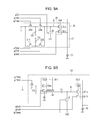
- FIGS. 5A to 5D are schematic diagrams illustrating energy bands in the photoelectric conversion unit 101 a .
- the energy bands of the first electrode 201 , the blocking layer 203 , the photoelectric conversion layer 205 , the insulating layer 207 , and the second electrode 209 are illustrated.
- a vertical axis in FIG. 5 represents a potential relative to electrons. The nearer to the top of FIG. 5 , the higher the potential relative to electrons. The nearer to the bottom of FIG. 5 , the lower the potential.
- the Fermi levels of the first electrode 201 and the second electrode 209 are illustrated.
- a band gap between the energy level of the conduction band and the energy level of the valence band is illustrated.
- the photoelectric conversion unit 101 a repeatedly performs the following process.
- the process includes steps (1) the reset of an input node of an amplification unit, (2) the reading of a noise signal, (3) the transfer of signal charges from a photoelectric conversion unit, (4) the reading of an optical signal, and (5) the storage of signal charges. These steps will be described below.
- FIG. 5A illustrates the state of the photoelectric conversion unit 101 a in steps (1) and (2).
- the potential Vs is supplied to the first electrode 201 .
- the first potential Vs is, for example, 3 V.
- the photoelectric conversion layer 205 stores holes represented by white circles as signal charges generated during exposure.
- the surface potential of the photoelectric conversion layer 205 on the side of the insulating layer 207 changes in accordance with the number of stored holes.
- the buffer circuit 12 a supplies a first potential Vd 1 to the capacitative element 12 b .
- the first potential Vd 1 is, for example, 0 V.
- the reset transistor 14 is turned on.
- the potential of a node including the second electrode 209 that is, the potential of the node FD
- the reset potential Vres is, for example, 1 V. Since the node FD is connected to the gate (input node) of the first amplification transistor 16 a , the input node of an amplification unit is reset.
- the reset transistor 14 is turned off.
- the node FD is brought into an electrically floating state.
- a reset noise may occur at the reset transistor 14 .
- holes of signal charges remain stored in the photoelectric conversion layer 205 .
- the selection transistor 16 b is turned on, so that the first amplification transistor 16 a outputs a noise signal including the reset noise.
- FIGS. 5B and 5C illustrates the state of the photoelectric conversion unit 101 a in step (3).
- the buffer circuit 12 a supplies a second potential Vd 2 to the capacitative element 12 b . Since holes are used as signal charges, the second potential Vd 2 is higher than the first potential Vd 1 .
- the second potential Vd 2 is, for example, 5 V.
- the potential of the second electrode 209 (the node FD) changes in the same direction in which a potential supplied by the buffer circuit 12 a changes.
- the amount of change dVB in the potential of the second electrode 209 is determined in accordance with the ratio between a capacitance value C 1 of the capacitative element 12 b electrically connected to the node FD and a capacitance value C 2 of the photoelectric conversion unit 101 a .
- the assumption that the capacitance values C 1 and C 2 are equal.
- the amount of change dVB in the potential of the second electrode 209 is sufficiently larger than the difference (Vs ⁇ Vres) between the potential Vs of the first electrode 201 and the reset potential Vres. Accordingly, the potential of the second electrode 209 is lower than that of the first electrode 201 and the potential gradient of the photoelectric conversion layer 205 is inverted. Electrons represented by a black circle are therefore injected from the first electrode 201 into the photoelectric conversion layer 205 . All or part of the holes stored in the photoelectric conversion layer 205 as signal charges move to the blocking layer 203 . The moved holes recombine with many carriers in the blocking layer 203 and disappear. As a result, holes are discharged from the photoelectric conversion layer 205 . When the photoelectric conversion layer 205 is entirely depleted, all of holes stored as signal charges are discharged from the photoelectric conversion layer 205 .
- the buffer circuit 12 a supplies the first potential Vd 1 to the capacitative element 12 b .
- the potential gradient of the photoelectric conversion layer 205 is inverted again.
- the electrons injected into the photoelectric conversion layer 205 in the state illustrated in FIG. 5B are therefore discharged from the photoelectric conversion layer 205 .
- the blocking layer 203 reduces the number of holes injected from the first electrode 201 into the photoelectric conversion layer 205 .
- the potential of the node FD is changed from a reset potential by a potential Vsig corresponding to the number of disappeared holes. That is, the potential Vsig corresponding to the number of holes stored as signal charges appears at the node FD.
- the potential Vsig corresponding to the number of stored holes is hereinafter referred to as an optical signal component.
- the selection transistor 16 b is turned on.
- the first amplification transistor 16 a outputs an optical signal.
- the difference between the noise signal read in step (2) and the optical signal read in step (4) is a signal based on the potential Vsig corresponding to stored signal charges.
- FIG. 5D illustrates the state of the photoelectric conversion unit 101 a in step (5).
- the potential Vs is supplied to the first electrode 201 , and the reset potential Vres is supplied to the node FD. Since the reset potential Vres is lower than the potential Vs of the first electrode 201 , electrons are discharged from the photoelectric conversion layer 205 to the first electrode 201 .
- holes in the photoelectric conversion layer 205 moves toward the interface between the photoelectric conversion layer 205 and the insulating layer 207 . However, since holes cannot move to the insulating layer 207 , the holes are stored in the photoelectric conversion layer 205 .
- the blocking layer 203 suppresses the injection of holes into the photoelectric conversion layer 205 .
- a potential Vch is the potential of the second electrode 209 changed in accordance with the number of holes stored in the photoelectric conversion layer 205 .
- the second potential Vd 2 is set to a potential lower than the first potential Vd 1 .
- the conductive type of the blocking layer 203 is set to a conductive type opposite to that of the blocking layer 203 according to this embodiment.
- the potential gradients illustrated in FIG. 5A to 5D are inverted. The other operations are not changed.
- FIG. 6 is a timing diagram illustrating the operation of the photoelectric conversion apparatus illustrated in FIG. 4A .
- Signals ⁇ Vp 1 , ⁇ Vp 2 , and ⁇ Vp 3 illustrated in FIG. 6 are supplied by the driving signal supply unit 4 to the pixels 10 in the first group, the second group, and the third group, respectively, as the signal ⁇ Vp illustrated in FIG. 4A .
- the period TRes illustrated in FIG. 6 is the same as that illustrated in FIG. 3 . That is, while the node FD is reset, the pixel processing unit 20 samples a noise signal.
- the driving signal supply unit 4 sets the signal level of the signal ⁇ Sel to Lo. As a result, the selection transistor 16 b is turned off. In a period TRf from a time t 5 to a time t 8 , the driving signal supply unit 4 changes the signal levels of the signals ⁇ Vp 1 , ⁇ Vp 2 , and ⁇ Vp 3 to Hi. As a result, the photoelectric conversion layer 205 is completely depleted. The node FD therefore has a potential based on charges stored in the photoelectric conversion layer 205 .
- the driving signal supply unit 4 sequentially sets the signal levels of the signals ⁇ Vp 1 , ⁇ Vp 2 , and ⁇ Vp 3 to Lo at times t 6 , t 7 , and t 8 , respectively.
- the driving signal supply unit 4 changes the signal level of the signal ⁇ Vp 1 from Hi to Lo and the signal level of the signal ⁇ Vp 2 from Lo to Hi.
- the driving signal supply unit 4 changes the signal level of the signal ⁇ Vp 2 from Hi to Lo and the signal level of the signal ⁇ Vp 3 from Lo to Hi.
- a photoelectric conversion apparatus sets a period in which the signal level of the signal ⁇ Vp is set to Hi for each group of the pixels 10 .
- a photoelectric conversion apparatus can therefore divide the load on the driving signal supply unit 4 for supplying the signal ⁇ Vp among a plurality of periods. Consequently, a photoelectric conversion apparatus according to this embodiment can more rapidly switch between the signal levels of the signal ⁇ Vp than a photoelectric conversion apparatus that supplies the common signal ⁇ Vp to all of the pixels 10 .
- the driving signal supply unit 4 makes a time at which the potential magnitude relationship between the first electrode and the second electrode in pixels in the first group is changed from the first relationship obtained in the period in which signal charges are discharged from the photoelectric conversion layer 205 to the second relationship opposite to the first relationship and a time at which the potential magnitude relationship between the first electrode and the second electrode in pixels in the second group is changed from the second relationship obtained in the period in which the photoelectric conversion layer 205 stores signal charges to the first relationship opposite to the second relationship overlap each other.
- the change in the potential of the node FD in the pixels 10 in the first group which occurs by the change in the signal level of the signal ⁇ Vp 1 from Hi to Lo is canceled by the change in the potential which occurs by the change in the signal level of the signal ⁇ Vp 2 from Lo to Hi. Accordingly, the change in the potential of the node FD in the pixels 10 in the first group which occurs by the change in the signal level of the signal ⁇ Vp 1 from Hi to Lo can be more rapidly converged as compared with a configuration in which there is no overlap between the change in the signal level of the signal ⁇ Vp 1 from Hi to Lo and the change in the signal level of the signal ⁇ Vp 2 from Lo to Hi. Consequently, a photoelectric conversion apparatus according to this embodiment can enhance the accuracy of an optical signal read after a time t 81 .
- the node FD in each pixel 10 in all rows has a potential based on charges stored in the photoelectric conversion layer 205 .
- the driving signal supply unit 4 sets the signal level of the signal ⁇ Sel to Hi.
- the driving signal supply unit 4 sequentially sets the signal levels of the signals ⁇ TS 1 , ⁇ TS 2 , and ⁇ TS 3 to Hi.
- the storage of an optical signal in the capacitative element CS is sequentially performed in the pixels 10 in the first group, the second group, and the third group.
- the capacitative element CS in each pixel 10 in all rows stores an optical signal.
- the vertical scanning circuit 3 causes the pixels 10 in each row to output corresponding optical signals and corresponding noise signals to the column signal processing circuit.
- the pixel processing unit 20 samples a noise signal while the node FD is reset. This leads to the reduction in the dark current component of the node FD included in a noise signal.
- a photoelectric conversion apparatus in a photoelectric conversion apparatus according to this embodiment, varies the time at which the signal level of the signal ⁇ Res, which is one of driving signals, is changed from Lo to hi from group to group.
- the column signal processing circuit can output a signal obtained by accurately subtracting the noise signal from the optical signal.
- the driving signal supply unit 4 sets the signal level of the signal ⁇ Sel to Lo when setting the signal level of the signal ⁇ Vp to Hi. That is, the first pixel output unit 16 is brought into a nonoperating state in a period in which the potential relationship between the first electrode 201 and the second electrode 209 in the photoelectric conversion unit 101 a is set to a relationship opposite to that in the period TRes and is set back to the same relationship as that in the period TRes. As a result, the change in the potential of the node B connected to the gate of the second amplification transistor 25 a can be suppressed.
- the second pixel output unit 25 outputs a noise signal stored in the capacitative element CN to the vertical signal line 17 in a state in which the potential of the node B is not stabilized.
- the signal level of the noise signal output to the vertical signal line 17 is therefore changed from the signal level of a noise signal assumed to be output when the potential of the node B is stabilized.
- the column signal processing circuit cannot accurately subtract the noise signal from an optical signal.
- a photoelectric conversion apparatus according to this embodiment can suppress the change in the potential of the node B caused by the change in the signal level of the signal ⁇ Vp, the second pixel output unit 25 can accurately the noise signal stored in the capacitative element CN even through a standby time until the change in the potential of the node B is stabilized is not provided.
- a photoelectric conversion apparatus according to this embodiment can achieve higher speed than a photoelectric conversion apparatus having a configuration in which the signal level of the signal ⁇ Sel is set to Hi during the change in the signal level of the signal ⁇ Vp.
- the potential of the second electrode 209 is changed in accordance with the signal level of the signal ⁇ Vp
- the potential of the first electrode 201 may be changed in accordance with the signal level of the signal ⁇ Vp 2 .
- a time at which the signal level of the signal ⁇ Vp 2 to be supplied to the pixels 10 in the first group is changed from Hi to Lo and a time at which the signal level of the signal ⁇ Vp 2 to be supplied to the pixels 10 in the second group is changed from Lo to Hi are made overlap each other.
- the potential magnitude relationship between the first electrode 201 and the second electrode 209 is set using the signal ⁇ Vp 2 so that it is opposite to the potential magnitude relationship between the first electrode 201 and the second electrode 209 in the period TRes.
- a photoelectric conversion apparatus will be described focusing on difference points between the second embodiment and the third embodiment.
- the configuration of a photoelectric conversion apparatus according to this embodiment is the same as that described in the second embodiment with reference to FIG. 4 .
- FIG. 7 is a timing diagram illustrating the operation of a photoelectric conversion apparatus according to this embodiment.
- a photoelectric conversion apparatus according to this embodiment sets a period in which the signal level of the signal ⁇ Sel is set to Hi for each group of the pixels 10 .
- the driving signal supply unit 4 changes the signal level of the signal Res 1 from Lo to Hi. As a result, the potential of the node FD is reset.
- the driving signal supply unit 4 changes the signal level of the signal ⁇ TN 1 to Hi.
- the first pixel output unit 16 in each pixel 10 in the first group outputs a noise signal to the capacitative element CN.
- the capacitative element CN in each pixel 10 in the first group stores the noise signal.
- the driving signal supply unit 4 sequentially sets the signal levels of the signals ⁇ Vp 1 , ⁇ Vp 2 , and ⁇ Vp 3 to Hi.
- the node FD in each pixel 10 in all rows illustrated in FIG. 1 has a potential based on signal charges that is stored by the photoelectric conversion unit 101 a in accordance with incident light.
- the signal level of the signal ⁇ Sel is Lo.
- the driving signal supply unit 4 changes the signal level of the signal ⁇ Sel- 1 to Hi. In a period from the time t 81 to the time t 82 , the driving signal supply unit 4 changes the signal level of the signal ⁇ TS 1 to Hi. At the time t 82 , the driving signal supply unit 4 changes the signal level of the signal ⁇ TS 1 to Lo. As a result, the capacitative element CS in each pixel 10 in the first group stores an optical signal.
- the driving signal supply unit 4 sets the signal levels of the signals ⁇ Sel- 2 and TS 2 to Hi.
- the driving signal supply unit 4 sets the signal level of the signal TS 2 to Lo.
- the capacitative element CS in each pixel 10 in the second group stores an optical signal.
- the driving signal supply unit 4 sets the signal levels of the signals ⁇ Sel- 3 and TS 3 to Hi.
- the driving signal supply unit 4 sets the signal level of the signal TS 3 to Lo.
- the capacitative element CS in each pixel 10 in the third group stores an optical signal.
- the switching between the operating state and the nonoperating state of the first pixel output unit 16 is performed for each group of the pixels 10 .
- the first pixel output units 16 in the other groups are brought into the nonoperating state. Accordingly, it is possible to reduce current consumption as compared with the operation illustrated in FIG. 6 .
- the driving signal supply unit 4 makes a time at which the potential magnitude relationship between the first electrode and the second electrode in pixels in the first group is changed to a relationship opposite to a relationship obtained in the period in which signal charges are discharged from the photoelectric conversion layer 205 and a time at which the potential magnitude relationship between the first electrode and the second electrode in pixels in the second group is changed to a relationship opposite to a relationship obtained in the period in which the photoelectric conversion layer 205 stores signal charges overlap each other.
- the change in the potential of the node FD in the pixels 10 in the first group which occurs by the change in the signal level of the signal ⁇ Vp 1 from Hi to Lo is canceled by the change in the potential which occurs by the change in the signal level of the signal ⁇ Vp 2 from Lo to Hi. Accordingly, the change in the potential of the node FD in the pixels 10 in the first group which occurs by the change in the signal level of the signal ⁇ Vp 1 from Hi to Lo can be more rapidly converged as compared with a configuration in which there is no overlap between the change in the signal level of the signal ⁇ Vp 1 from Hi to Lo and the change in the signal level of the signal ⁇ Vp 2 from Lo to Hi. Consequently, a photoelectric conversion apparatus according to this embodiment can enhance the accuracy of an optical signal read after the time t 81 .
- FIG. 8 is a timing diagram illustrating another operation of a photoelectric conversion apparatus according to this embodiment.
- a time at which the signal level of the signal ⁇ Res 1 is changed from Hi to Lo and a time at which the signal level of the signal ⁇ Res 2 is changed from Lo to Hi are the same.
- a time at which the signal level of the signal ⁇ Res 2 is changed from Hi to Lo and a time at which the signal level of the signal ⁇ Res 3 is changed from Lo to Hi are the same.
- a period in which the signal ⁇ Sel is set to Hi and a period in which the signal ⁇ Res is set to Hi vary from group to group.
- a period in which the signal level of the signal ⁇ Vp is set to Hi may vary from group to group. That is, the period in which the signal ⁇ Sel is set to Hi may be the same in all groups, and the period in which the signal ⁇ Res is set to Hi may be the same in all groups.
- Photoelectric conversion apparatuses described in the first to third embodiments can be applied to various photoelectric conversion systems.
- Examples of a photoelectric conversion system include a digital still camera, a digital camcorder, and a surveillance camera.
- FIG. 9 is a schematic diagram of a digital still camera that is an example of a photoelectric conversion system to which a photoelectric conversion apparatus according to the first, second, or third embodiment is applied.
- a photoelectric conversion system illustrated in FIG. 11 includes a photoelectric conversion apparatus 154 , a barrier 151 for protecting a lens, a lens 152 for forming an optical image of a subject on the photoelectric conversion apparatus 154 , and a diaphragm 153 for changing the amount of light passing through the lens 152 .
- the lens 152 and the diaphragm 153 are optical systems for concentrating light on the photoelectric conversion apparatus 154 .
- the photoelectric conversion system illustrated in FIG. 11 further includes an output signal processing unit 155 for processing a signal output from the photoelectric conversion apparatus 154 .
- the output signal processing unit 155 converts an analog signal output from the photoelectric conversion apparatus 154 into a digital signal. In addition, the output signal processing unit 155 performs various corrections and various compressions as needed and outputs image data.
- the photoelectric conversion system illustrated in FIG. 11 further includes a buffer memory unit 156 for temporarily storing image data, an external interface (I/F) unit 157 for communicating with an external computer, a recording medium 159 such as a semiconductor memory in which image data is recorded or from which image data is read, and a recording medium control I/F unit 158 used for the recording of image data in the recording medium 159 or the reading of image data from the recording medium 159 .
- the recording medium 159 may be built into the photoelectric conversion system or may be detachable.
- the photoelectric conversion system further includes an overall control/computation unit 1510 for performing various pieces of computation and overall control of the digital still camera and a timing generation unit 1511 for outputting various timing signals to the photoelectric conversion apparatus 154 and the output signal processing unit 155 .
- Timing signals may be externally input into the photoelectric conversion system.
- the photoelectric conversion system may include at least the photoelectric conversion apparatus 154 and the output signal processing unit 155 for processing a signal output from the photoelectric conversion apparatus 154 .
- a photoelectric conversion system according to this embodiment can perform an image capturing operation using the photoelectric conversion apparatus 154 .
- the signal-to-noise ratio of a signal output from a pixel can be improved.
Landscapes
- Engineering & Computer Science (AREA)
- Multimedia (AREA)
- Signal Processing (AREA)
- Solid State Image Pick-Up Elements (AREA)
- Transforming Light Signals Into Electric Signals (AREA)
Applications Claiming Priority (2)
| Application Number | Priority Date | Filing Date | Title |
|---|---|---|---|
| JP2014163207A JP6501462B2 (ja) | 2014-08-08 | 2014-08-08 | 光電変換装置及び光電変換装置の駆動方法 |
| JP2014-163207 | 2014-08-08 |
Publications (2)
| Publication Number | Publication Date |
|---|---|
| US20160044263A1 US20160044263A1 (en) | 2016-02-11 |
| US9723236B2 true US9723236B2 (en) | 2017-08-01 |
Family
ID=55268409
Family Applications (1)
| Application Number | Title | Priority Date | Filing Date |
|---|---|---|---|
| US14/819,085 Expired - Fee Related US9723236B2 (en) | 2014-08-08 | 2015-08-05 | Photoelectric conversion apparatus and method for driving photoelectric conversion apparatus |
Country Status (2)
| Country | Link |
|---|---|
| US (1) | US9723236B2 (enExample) |
| JP (1) | JP6501462B2 (enExample) |
Cited By (1)
| Publication number | Priority date | Publication date | Assignee | Title |
|---|---|---|---|---|
| US12003872B2 (en) * | 2015-12-03 | 2024-06-04 | Panasonic Intellectual Property Management Co., Ltd. | Imaging device including photoelectric conversion layer |
Families Citing this family (13)
| Publication number | Priority date | Publication date | Assignee | Title |
|---|---|---|---|---|
| JP6808463B2 (ja) | 2016-11-30 | 2021-01-06 | キヤノン株式会社 | 光電変換装置および光電変換システム |
| US10930709B2 (en) | 2017-10-03 | 2021-02-23 | Lockheed Martin Corporation | Stacked transparent pixel structures for image sensors |
| US10249800B1 (en) | 2017-10-03 | 2019-04-02 | Lockheed Martin Corporation | Stacked transparent pixel structures for electronic displays |
| US10510812B2 (en) | 2017-11-09 | 2019-12-17 | Lockheed Martin Corporation | Display-integrated infrared emitter and sensor structures |
| US10690910B2 (en) | 2018-02-07 | 2020-06-23 | Lockheed Martin Corporation | Plenoptic cellular vision correction |
| US10594951B2 (en) | 2018-02-07 | 2020-03-17 | Lockheed Martin Corporation | Distributed multi-aperture camera array |
| US10979699B2 (en) | 2018-02-07 | 2021-04-13 | Lockheed Martin Corporation | Plenoptic cellular imaging system |
| US11616941B2 (en) | 2018-02-07 | 2023-03-28 | Lockheed Martin Corporation | Direct camera-to-display system |
| US10838250B2 (en) | 2018-02-07 | 2020-11-17 | Lockheed Martin Corporation | Display assemblies with electronically emulated transparency |
| US10951883B2 (en) | 2018-02-07 | 2021-03-16 | Lockheed Martin Corporation | Distributed multi-screen array for high density display |
| US10652529B2 (en) | 2018-02-07 | 2020-05-12 | Lockheed Martin Corporation | In-layer Signal processing |
| US10866413B2 (en) | 2018-12-03 | 2020-12-15 | Lockheed Martin Corporation | Eccentric incident luminance pupil tracking |
| US10698201B1 (en) | 2019-04-02 | 2020-06-30 | Lockheed Martin Corporation | Plenoptic cellular axis redirection |
Citations (6)
| Publication number | Priority date | Publication date | Assignee | Title |
|---|---|---|---|---|
| JPH08116044A (ja) | 1993-12-27 | 1996-05-07 | Canon Inc | 光電変換装置、その駆動方法及びそれを有するシステム |
| JP2001074551A (ja) | 1999-09-02 | 2001-03-23 | Canon Inc | 光電変換装置及びその駆動方法 |
| US20010024844A1 (en) * | 1997-11-04 | 2001-09-27 | Isao Kobayashi | Photoelectric converter, method for driving photoelectric converter and system having photoelectric converter |
| JP2007104219A (ja) | 2005-10-03 | 2007-04-19 | Canon Inc | 放射線撮影装置及びその制御方法、放射線撮影システム |
| JP2009063514A (ja) | 2007-09-07 | 2009-03-26 | Canon Inc | 撮像装置及び放射線撮像システム |
| JP2012204966A (ja) | 2011-03-24 | 2012-10-22 | Canon Inc | 撮像装置及び撮像システム、その制御方法 |
Family Cites Families (3)
| Publication number | Priority date | Publication date | Assignee | Title |
|---|---|---|---|---|
| JP4208482B2 (ja) * | 2002-05-08 | 2009-01-14 | キヤノン株式会社 | 撮像装置及び同撮像装置を用いたx線診断システム |
| JP5335385B2 (ja) * | 2008-11-20 | 2013-11-06 | キヤノン株式会社 | 放射線検出器、半導体撮像素子アレイおよび制御方法 |
| JP5995661B2 (ja) * | 2012-10-31 | 2016-09-21 | 富士フイルム株式会社 | 半導体膜、半導体膜の製造方法、太陽電池、発光ダイオード、薄膜トランジスタおよび電子デバイス |
-
2014
- 2014-08-08 JP JP2014163207A patent/JP6501462B2/ja not_active Expired - Fee Related
-
2015
- 2015-08-05 US US14/819,085 patent/US9723236B2/en not_active Expired - Fee Related
Patent Citations (6)
| Publication number | Priority date | Publication date | Assignee | Title |
|---|---|---|---|---|
| JPH08116044A (ja) | 1993-12-27 | 1996-05-07 | Canon Inc | 光電変換装置、その駆動方法及びそれを有するシステム |
| US20010024844A1 (en) * | 1997-11-04 | 2001-09-27 | Isao Kobayashi | Photoelectric converter, method for driving photoelectric converter and system having photoelectric converter |
| JP2001074551A (ja) | 1999-09-02 | 2001-03-23 | Canon Inc | 光電変換装置及びその駆動方法 |
| JP2007104219A (ja) | 2005-10-03 | 2007-04-19 | Canon Inc | 放射線撮影装置及びその制御方法、放射線撮影システム |
| JP2009063514A (ja) | 2007-09-07 | 2009-03-26 | Canon Inc | 撮像装置及び放射線撮像システム |
| JP2012204966A (ja) | 2011-03-24 | 2012-10-22 | Canon Inc | 撮像装置及び撮像システム、その制御方法 |
Cited By (1)
| Publication number | Priority date | Publication date | Assignee | Title |
|---|---|---|---|---|
| US12003872B2 (en) * | 2015-12-03 | 2024-06-04 | Panasonic Intellectual Property Management Co., Ltd. | Imaging device including photoelectric conversion layer |
Also Published As
| Publication number | Publication date |
|---|---|
| JP6501462B2 (ja) | 2019-04-17 |
| JP2016039580A (ja) | 2016-03-22 |
| US20160044263A1 (en) | 2016-02-11 |
Similar Documents
| Publication | Publication Date | Title |
|---|---|---|
| US9723236B2 (en) | Photoelectric conversion apparatus and method for driving photoelectric conversion apparatus | |
| US9826181B2 (en) | Photoelectric conversion device and imaging system | |
| US9722107B2 (en) | Photoelectric conversion device and imaging system | |
| US9941315B2 (en) | Photoelectric conversion device and imaging system | |
| US10645327B2 (en) | Solid-state imaging device, method for driving solid-state imaging device, and electronic apparatus | |
| US20170366775A1 (en) | Photoelectric conversion apparatus, photoelectric conversion system, and driving method for the photoelectric conversion apparatus | |
| JP7000020B2 (ja) | 光電変換装置、撮像システム | |
| US9866774B2 (en) | Photoelectric conversion device and imaging system | |
| US10368016B2 (en) | Photoelectric conversion device and imaging system | |
| US10091444B2 (en) | Photoelectric conversion apparatus and photoelectric conversion system | |
| US8957360B2 (en) | Method for driving photoelectric conversion apparatus | |
| US9807329B2 (en) | Imaging device and imaging system | |
| US20130215310A1 (en) | Method for driving photoelectric conversion apparatus | |
| US8520109B2 (en) | Solid-state image pickup apparatus and image pickup system | |
| JP2017098815A (ja) | 光電変換装置、および、撮像システム | |
| JP6703053B2 (ja) | 光電変換装置、光電変換システム | |
| WO2023079795A1 (ja) | 撮像装置 |
Legal Events
| Date | Code | Title | Description |
|---|---|---|---|
| AS | Assignment |
Owner name: CANON KABUSHIKI KAISHA, JAPAN Free format text: ASSIGNMENT OF ASSIGNORS INTEREST;ASSIGNORS:HASHIMOTO, SEIJI;TAKAHASHI, HIDEKAZU;FURUBAYASHI, ATSUSHI;SIGNING DATES FROM 20150710 TO 20150718;REEL/FRAME:036851/0237 |
|
| STCF | Information on status: patent grant |
Free format text: PATENTED CASE |
|
| MAFP | Maintenance fee payment |
Free format text: PAYMENT OF MAINTENANCE FEE, 4TH YEAR, LARGE ENTITY (ORIGINAL EVENT CODE: M1551); ENTITY STATUS OF PATENT OWNER: LARGE ENTITY Year of fee payment: 4 |
|
| FEPP | Fee payment procedure |
Free format text: MAINTENANCE FEE REMINDER MAILED (ORIGINAL EVENT CODE: REM.); ENTITY STATUS OF PATENT OWNER: LARGE ENTITY |
|
| LAPS | Lapse for failure to pay maintenance fees |
Free format text: PATENT EXPIRED FOR FAILURE TO PAY MAINTENANCE FEES (ORIGINAL EVENT CODE: EXP.); ENTITY STATUS OF PATENT OWNER: LARGE ENTITY |
|
| STCH | Information on status: patent discontinuation |
Free format text: PATENT EXPIRED DUE TO NONPAYMENT OF MAINTENANCE FEES UNDER 37 CFR 1.362 |
|
| FP | Lapsed due to failure to pay maintenance fee |
Effective date: 20250801 |