US9691815B2 - Method for producing an optoelectronic semiconductor component, and optoelectronic semiconductor component - Google Patents
Method for producing an optoelectronic semiconductor component, and optoelectronic semiconductor component Download PDFInfo
- Publication number
- US9691815B2 US9691815B2 US14/434,760 US201314434760A US9691815B2 US 9691815 B2 US9691815 B2 US 9691815B2 US 201314434760 A US201314434760 A US 201314434760A US 9691815 B2 US9691815 B2 US 9691815B2
- Authority
- US
- United States
- Prior art keywords
- islands
- layer
- growth substrate
- electrical contact
- separating
- Prior art date
- Legal status (The legal status is an assumption and is not a legal conclusion. Google has not performed a legal analysis and makes no representation as to the accuracy of the status listed.)
- Active
Links
- 239000004065 semiconductor Substances 0.000 title claims abstract description 74
- 230000005693 optoelectronics Effects 0.000 title claims description 20
- 238000004519 manufacturing process Methods 0.000 title claims description 8
- 239000000758 substrate Substances 0.000 claims abstract description 147
- 238000000034 method Methods 0.000 claims abstract description 50
- 238000011049 filling Methods 0.000 claims description 36
- 239000000463 material Substances 0.000 claims description 30
- 150000001875 compounds Chemical class 0.000 claims description 25
- 230000005855 radiation Effects 0.000 claims description 23
- 230000000873 masking effect Effects 0.000 claims description 21
- 230000002093 peripheral effect Effects 0.000 claims description 5
- VYPSYNLAJGMNEJ-UHFFFAOYSA-N Silicium dioxide Chemical compound O=[Si]=O VYPSYNLAJGMNEJ-UHFFFAOYSA-N 0.000 description 11
- 238000002161 passivation Methods 0.000 description 11
- 238000005530 etching Methods 0.000 description 9
- 230000000694 effects Effects 0.000 description 8
- 239000002131 composite material Substances 0.000 description 5
- 229910052751 metal Inorganic materials 0.000 description 5
- 239000002184 metal Substances 0.000 description 5
- 238000000926 separation method Methods 0.000 description 5
- XUIMIQQOPSSXEZ-UHFFFAOYSA-N Silicon Chemical compound [Si] XUIMIQQOPSSXEZ-UHFFFAOYSA-N 0.000 description 4
- 239000000470 constituent Substances 0.000 description 4
- 239000011258 core-shell material Substances 0.000 description 4
- 229910052710 silicon Inorganic materials 0.000 description 4
- 239000010703 silicon Substances 0.000 description 4
- 239000000377 silicon dioxide Substances 0.000 description 4
- 229910002704 AlGaN Inorganic materials 0.000 description 3
- PNEYBMLMFCGWSK-UHFFFAOYSA-N Alumina Chemical compound [O-2].[O-2].[O-2].[Al+3].[Al+3] PNEYBMLMFCGWSK-UHFFFAOYSA-N 0.000 description 3
- 229910052581 Si3N4 Inorganic materials 0.000 description 3
- 229910052681 coesite Inorganic materials 0.000 description 3
- 229910052906 cristobalite Inorganic materials 0.000 description 3
- 230000002950 deficient Effects 0.000 description 3
- 239000000945 filler Substances 0.000 description 3
- HQVNEWCFYHHQES-UHFFFAOYSA-N silicon nitride Chemical compound N12[Si]34N5[Si]62N3[Si]51N64 HQVNEWCFYHHQES-UHFFFAOYSA-N 0.000 description 3
- 229910052814 silicon oxide Inorganic materials 0.000 description 3
- 229910052682 stishovite Inorganic materials 0.000 description 3
- 229910052719 titanium Inorganic materials 0.000 description 3
- 239000010936 titanium Substances 0.000 description 3
- 229910052905 tridymite Inorganic materials 0.000 description 3
- 229910017083 AlN Inorganic materials 0.000 description 2
- PIGFYZPCRLYGLF-UHFFFAOYSA-N Aluminum nitride Chemical compound [Al]#N PIGFYZPCRLYGLF-UHFFFAOYSA-N 0.000 description 2
- IJGRMHOSHXDMSA-UHFFFAOYSA-N Atomic nitrogen Chemical compound N#N IJGRMHOSHXDMSA-UHFFFAOYSA-N 0.000 description 2
- GWEVSGVZZGPLCZ-UHFFFAOYSA-N Titan oxide Chemical compound O=[Ti]=O GWEVSGVZZGPLCZ-UHFFFAOYSA-N 0.000 description 2
- 239000011358 absorbing material Substances 0.000 description 2
- 229910052782 aluminium Inorganic materials 0.000 description 2
- 229910052785 arsenic Inorganic materials 0.000 description 2
- 239000004020 conductor Substances 0.000 description 2
- 239000013078 crystal Substances 0.000 description 2
- 229910052733 gallium Inorganic materials 0.000 description 2
- 229910052738 indium Inorganic materials 0.000 description 2
- 239000000203 mixture Substances 0.000 description 2
- 229910052759 nickel Inorganic materials 0.000 description 2
- 229910052757 nitrogen Inorganic materials 0.000 description 2
- 229910052594 sapphire Inorganic materials 0.000 description 2
- 239000010980 sapphire Substances 0.000 description 2
- 230000003595 spectral effect Effects 0.000 description 2
- 239000000126 substance Substances 0.000 description 2
- OGIDPMRJRNCKJF-UHFFFAOYSA-N titanium oxide Inorganic materials [Ti]=O OGIDPMRJRNCKJF-UHFFFAOYSA-N 0.000 description 2
- 230000007704 transition Effects 0.000 description 2
- 229910052721 tungsten Inorganic materials 0.000 description 2
- 238000002604 ultrasonography Methods 0.000 description 2
- 229910002601 GaN Inorganic materials 0.000 description 1
- GYHNNYVSQQEPJS-UHFFFAOYSA-N Gallium Chemical compound [Ga] GYHNNYVSQQEPJS-UHFFFAOYSA-N 0.000 description 1
- UFHFLCQGNIYNRP-UHFFFAOYSA-N Hydrogen Chemical compound [H][H] UFHFLCQGNIYNRP-UHFFFAOYSA-N 0.000 description 1
- ZOKXTWBITQBERF-UHFFFAOYSA-N Molybdenum Chemical compound [Mo] ZOKXTWBITQBERF-UHFFFAOYSA-N 0.000 description 1
- BQCADISMDOOEFD-UHFFFAOYSA-N Silver Chemical compound [Ag] BQCADISMDOOEFD-UHFFFAOYSA-N 0.000 description 1
- RTAQQCXQSZGOHL-UHFFFAOYSA-N Titanium Chemical compound [Ti] RTAQQCXQSZGOHL-UHFFFAOYSA-N 0.000 description 1
- NRTOMJZYCJJWKI-UHFFFAOYSA-N Titanium nitride Chemical compound [Ti]#N NRTOMJZYCJJWKI-UHFFFAOYSA-N 0.000 description 1
- 238000010521 absorption reaction Methods 0.000 description 1
- 239000011149 active material Substances 0.000 description 1
- 238000000149 argon plasma sintering Methods 0.000 description 1
- RQNWIZPPADIBDY-UHFFFAOYSA-N arsenic atom Chemical compound [As] RQNWIZPPADIBDY-UHFFFAOYSA-N 0.000 description 1
- QVGXLLKOCUKJST-UHFFFAOYSA-N atomic oxygen Chemical compound [O] QVGXLLKOCUKJST-UHFFFAOYSA-N 0.000 description 1
- UMIVXZPTRXBADB-UHFFFAOYSA-N benzocyclobutene Chemical compound C1=CC=C2CCC2=C1 UMIVXZPTRXBADB-UHFFFAOYSA-N 0.000 description 1
- 239000012876 carrier material Substances 0.000 description 1
- 239000000919 ceramic Substances 0.000 description 1
- 238000004140 cleaning Methods 0.000 description 1
- 239000011248 coating agent Substances 0.000 description 1
- 238000000576 coating method Methods 0.000 description 1
- 230000001427 coherent effect Effects 0.000 description 1
- 230000006378 damage Effects 0.000 description 1
- 230000009849 deactivation Effects 0.000 description 1
- 230000001419 dependent effect Effects 0.000 description 1
- 230000008021 deposition Effects 0.000 description 1
- 238000011161 development Methods 0.000 description 1
- 230000018109 developmental process Effects 0.000 description 1
- 239000002019 doping agent Substances 0.000 description 1
- 238000010292 electrical insulation Methods 0.000 description 1
- 239000012777 electrically insulating material Substances 0.000 description 1
- 239000007789 gas Substances 0.000 description 1
- 239000011521 glass Substances 0.000 description 1
- 239000001257 hydrogen Substances 0.000 description 1
- 229910052739 hydrogen Inorganic materials 0.000 description 1
- APFVFJFRJDLVQX-UHFFFAOYSA-N indium atom Chemical compound [In] APFVFJFRJDLVQX-UHFFFAOYSA-N 0.000 description 1
- AMGQUBHHOARCQH-UHFFFAOYSA-N indium;oxotin Chemical compound [In].[Sn]=O AMGQUBHHOARCQH-UHFFFAOYSA-N 0.000 description 1
- 238000009413 insulation Methods 0.000 description 1
- 230000001788 irregular Effects 0.000 description 1
- 238000002955 isolation Methods 0.000 description 1
- 238000011068 loading method Methods 0.000 description 1
- 229910001092 metal group alloy Inorganic materials 0.000 description 1
- 229910052750 molybdenum Inorganic materials 0.000 description 1
- 239000011733 molybdenum Substances 0.000 description 1
- PXHVJJICTQNCMI-UHFFFAOYSA-N nickel Substances [Ni] PXHVJJICTQNCMI-UHFFFAOYSA-N 0.000 description 1
- 150000004767 nitrides Chemical class 0.000 description 1
- 230000003287 optical effect Effects 0.000 description 1
- 239000001301 oxygen Substances 0.000 description 1
- 229910052760 oxygen Inorganic materials 0.000 description 1
- 229910052698 phosphorus Inorganic materials 0.000 description 1
- 230000000704 physical effect Effects 0.000 description 1
- 239000004033 plastic Substances 0.000 description 1
- 239000002985 plastic film Substances 0.000 description 1
- 229920006255 plastic film Polymers 0.000 description 1
- 229920000052 poly(p-xylylene) Polymers 0.000 description 1
- 229920000642 polymer Polymers 0.000 description 1
- 229920001296 polysiloxane Polymers 0.000 description 1
- 238000007788 roughening Methods 0.000 description 1
- 235000012239 silicon dioxide Nutrition 0.000 description 1
- 229910052709 silver Inorganic materials 0.000 description 1
- 239000004332 silver Substances 0.000 description 1
- 238000005476 soldering Methods 0.000 description 1
- 230000003019 stabilising effect Effects 0.000 description 1
- 229910052714 tellurium Inorganic materials 0.000 description 1
- PORWMNRCUJJQNO-UHFFFAOYSA-N tellurium atom Chemical compound [Te] PORWMNRCUJJQNO-UHFFFAOYSA-N 0.000 description 1
- 230000008646 thermal stress Effects 0.000 description 1
- 239000010937 tungsten Substances 0.000 description 1
- -1 tungsten nitride Chemical class 0.000 description 1
- 238000003631 wet chemical etching Methods 0.000 description 1
- XLOMVQKBTHCTTD-UHFFFAOYSA-N zinc oxide Inorganic materials [Zn]=O XLOMVQKBTHCTTD-UHFFFAOYSA-N 0.000 description 1
Images


Classifications
-
- H—ELECTRICITY
- H01—ELECTRIC ELEMENTS
- H01L—SEMICONDUCTOR DEVICES NOT COVERED BY CLASS H10
- H01L27/00—Devices consisting of a plurality of semiconductor or other solid-state components formed in or on a common substrate
- H01L27/15—Devices consisting of a plurality of semiconductor or other solid-state components formed in or on a common substrate including semiconductor components having potential barriers, specially adapted for light emission
- H01L27/153—Devices consisting of a plurality of semiconductor or other solid-state components formed in or on a common substrate including semiconductor components having potential barriers, specially adapted for light emission in a repetitive configuration, e.g. LED bars
- H01L27/156—Devices consisting of a plurality of semiconductor or other solid-state components formed in or on a common substrate including semiconductor components having potential barriers, specially adapted for light emission in a repetitive configuration, e.g. LED bars two-dimensional arrays
-
- H—ELECTRICITY
- H01—ELECTRIC ELEMENTS
- H01L—SEMICONDUCTOR DEVICES NOT COVERED BY CLASS H10
- H01L33/00—Semiconductor devices having potential barriers specially adapted for light emission; Processes or apparatus specially adapted for the manufacture or treatment thereof or of parts thereof; Details thereof
- H01L33/005—Processes
- H01L33/0062—Processes for devices with an active region comprising only III-V compounds
-
- H01L33/0079—
-
- H—ELECTRICITY
- H01—ELECTRIC ELEMENTS
- H01L—SEMICONDUCTOR DEVICES NOT COVERED BY CLASS H10
- H01L33/00—Semiconductor devices having potential barriers specially adapted for light emission; Processes or apparatus specially adapted for the manufacture or treatment thereof or of parts thereof; Details thereof
- H01L33/005—Processes
- H01L33/0093—Wafer bonding; Removal of the growth substrate
-
- H—ELECTRICITY
- H01—ELECTRIC ELEMENTS
- H01L—SEMICONDUCTOR DEVICES NOT COVERED BY CLASS H10
- H01L33/00—Semiconductor devices having potential barriers specially adapted for light emission; Processes or apparatus specially adapted for the manufacture or treatment thereof or of parts thereof; Details thereof
- H01L33/02—Semiconductor devices having potential barriers specially adapted for light emission; Processes or apparatus specially adapted for the manufacture or treatment thereof or of parts thereof; Details thereof characterised by the semiconductor bodies
- H01L33/20—Semiconductor devices having potential barriers specially adapted for light emission; Processes or apparatus specially adapted for the manufacture or treatment thereof or of parts thereof; Details thereof characterised by the semiconductor bodies with a particular shape, e.g. curved or truncated substrate
- H01L33/24—Semiconductor devices having potential barriers specially adapted for light emission; Processes or apparatus specially adapted for the manufacture or treatment thereof or of parts thereof; Details thereof characterised by the semiconductor bodies with a particular shape, e.g. curved or truncated substrate of the light emitting region, e.g. non-planar junction
-
- H—ELECTRICITY
- H01—ELECTRIC ELEMENTS
- H01L—SEMICONDUCTOR DEVICES NOT COVERED BY CLASS H10
- H01L25/00—Assemblies consisting of a plurality of individual semiconductor or other solid state devices ; Multistep manufacturing processes thereof
- H01L25/03—Assemblies consisting of a plurality of individual semiconductor or other solid state devices ; Multistep manufacturing processes thereof all the devices being of a type provided for in the same subgroup of groups H01L27/00 - H01L33/00, or in a single subclass of H10K, H10N, e.g. assemblies of rectifier diodes
- H01L25/04—Assemblies consisting of a plurality of individual semiconductor or other solid state devices ; Multistep manufacturing processes thereof all the devices being of a type provided for in the same subgroup of groups H01L27/00 - H01L33/00, or in a single subclass of H10K, H10N, e.g. assemblies of rectifier diodes the devices not having separate containers
- H01L25/075—Assemblies consisting of a plurality of individual semiconductor or other solid state devices ; Multistep manufacturing processes thereof all the devices being of a type provided for in the same subgroup of groups H01L27/00 - H01L33/00, or in a single subclass of H10K, H10N, e.g. assemblies of rectifier diodes the devices not having separate containers the devices being of a type provided for in group H01L33/00
- H01L25/0753—Assemblies consisting of a plurality of individual semiconductor or other solid state devices ; Multistep manufacturing processes thereof all the devices being of a type provided for in the same subgroup of groups H01L27/00 - H01L33/00, or in a single subclass of H10K, H10N, e.g. assemblies of rectifier diodes the devices not having separate containers the devices being of a type provided for in group H01L33/00 the devices being arranged next to each other
-
- H—ELECTRICITY
- H01—ELECTRIC ELEMENTS
- H01L—SEMICONDUCTOR DEVICES NOT COVERED BY CLASS H10
- H01L2924/00—Indexing scheme for arrangements or methods for connecting or disconnecting semiconductor or solid-state bodies as covered by H01L24/00
-
- H—ELECTRICITY
- H01—ELECTRIC ELEMENTS
- H01L—SEMICONDUCTOR DEVICES NOT COVERED BY CLASS H10
- H01L2924/00—Indexing scheme for arrangements or methods for connecting or disconnecting semiconductor or solid-state bodies as covered by H01L24/00
- H01L2924/0001—Technical content checked by a classifier
- H01L2924/0002—Not covered by any one of groups H01L24/00, H01L24/00 and H01L2224/00
-
- H—ELECTRICITY
- H01—ELECTRIC ELEMENTS
- H01L—SEMICONDUCTOR DEVICES NOT COVERED BY CLASS H10
- H01L33/00—Semiconductor devices having potential barriers specially adapted for light emission; Processes or apparatus specially adapted for the manufacture or treatment thereof or of parts thereof; Details thereof
- H01L33/02—Semiconductor devices having potential barriers specially adapted for light emission; Processes or apparatus specially adapted for the manufacture or treatment thereof or of parts thereof; Details thereof characterised by the semiconductor bodies
- H01L33/16—Semiconductor devices having potential barriers specially adapted for light emission; Processes or apparatus specially adapted for the manufacture or treatment thereof or of parts thereof; Details thereof characterised by the semiconductor bodies with a particular crystal structure or orientation, e.g. polycrystalline, amorphous or porous
- H01L33/18—Semiconductor devices having potential barriers specially adapted for light emission; Processes or apparatus specially adapted for the manufacture or treatment thereof or of parts thereof; Details thereof characterised by the semiconductor bodies with a particular crystal structure or orientation, e.g. polycrystalline, amorphous or porous within the light emitting region
-
- H—ELECTRICITY
- H01—ELECTRIC ELEMENTS
- H01L—SEMICONDUCTOR DEVICES NOT COVERED BY CLASS H10
- H01L33/00—Semiconductor devices having potential barriers specially adapted for light emission; Processes or apparatus specially adapted for the manufacture or treatment thereof or of parts thereof; Details thereof
- H01L33/36—Semiconductor devices having potential barriers specially adapted for light emission; Processes or apparatus specially adapted for the manufacture or treatment thereof or of parts thereof; Details thereof characterised by the electrodes
- H01L33/38—Semiconductor devices having potential barriers specially adapted for light emission; Processes or apparatus specially adapted for the manufacture or treatment thereof or of parts thereof; Details thereof characterised by the electrodes with a particular shape
- H01L33/385—Semiconductor devices having potential barriers specially adapted for light emission; Processes or apparatus specially adapted for the manufacture or treatment thereof or of parts thereof; Details thereof characterised by the electrodes with a particular shape the electrode extending at least partially onto a side surface of the semiconductor body
Definitions
- a method for producing an optoelectronic semiconductor component is provided. Furthermore, an optoelectronic semiconductor component produced thereby is provided.
- An object to be achieved resides in the provision of an optoelectronic semiconductor component which has a high efficiency with large operating currents.
- the method is adapted for producing an optoelectronic semiconductor component.
- the semiconductor component is, for example, a light-emitting diode.
- the semiconductor component is configured for producing ultraviolet radiation, visible light and/or near-infrared radiation during operation.
- the method includes the step of producing radiation-active islands.
- the islands have a semiconductor layer sequence.
- the semiconductor layer sequence is preferably based on a III-V-composite semiconductor material.
- the semiconductor material is, for example, a nitride composite semiconductor material such as Al n In 1-n-m Ga m N or a phosphide composite semiconductor material such as Al n In 1-n-m Ga m P or even an arsenic composite semiconductor material such as Al n In 1-n-m Ga m As, wherein in each case 0 ⁇ n ⁇ 1, 0 ⁇ m ⁇ 1 and n+m ⁇ 1.
- the semiconductor layer sequence can comprise dopants and additional constituents.
- the semiconductor layer sequence is based on AlInGaN.
- the islands are produced indirectly or directly on a growth substrate.
- the growth substrate is, for example, a sapphire substrate or a silicon substrate.
- the islands are formed, for example, by self-organised, three-dimensional growth, by selective growing on the growth substrate by means of a growth mask or by overgrowing of three-dimensional structures.
- Such three-dimensional structures can be produced from a two-dimensional layer for instance by means of etching.
- the islands each comprise one or more active zones.
- the active zone is preferably a constituent of the semiconductor layer sequence and is located, for example, between a p-type layer and an n-type layer of the semiconductor layer sequence.
- the active zone can be a single, inherently coherent area of the semiconductor layer sequence having constant physical properties perpendicular to a major axis, within manufacturing tolerances.
- the composition and/or a thickness of the active zones can gradually or suddenly change. Different crystal facets along core-shell structures can likewise result in differences in the design of the active zone.
- the thickness of the active zone in core-shell structures preferably amounts to at least 2 nm and/or at the most to 40 nm. In axial structures, the thickness of the active zone can even be up to 1000 nm.
- the active zone can be a single quantum well structure or a multiple quantum well structure.
- an average diameter of the islands amounts to at least 50 nm or to at least 100 nm or to at least 200 nm. Alternatively or in addition, the average diameter amounts at the most to 10 ⁇ m or at the most to 5 ⁇ m or at the most to 3 ⁇ m or at the most to 2 ⁇ m. As viewed in a top view, the islands have, for example, a round or polygonal outline, in particular a hexagonal outline.
- the method includes the step of producing a separating layer indirectly or directly on a side of the islands facing the growth substrate.
- the separating layer is configured for permitting the detachment of the islands from the growth substrate.
- the separating layer can, in the direction towards the growth substrate, terminate flush with the islands and extend as an extension of root points or growth points of the islands and/or a sacrificial layer of the islands.
- the separating layer surrounds the islands or at least part of the islands all around, as viewed in a top view of the growth substrate. This is particularly the case after the separating layer has been produced and/or structured or after a partial material deposition of the separating layer after applying material of the separating layer.
- the separating layer is then a contiguous layer in which a multiplicity of holes are formed, as viewed in a top view, wherein the islands are located in the holes of the separating layer and/or are grown out of the holes.
- the method comprises the step of attaching a carrier substrate.
- the carrier substrate is applied to a side of the islands facing away from the growth substrate.
- the carrier substrate can touch the islands or be spaced apart from the islands by at least one intermediate layer. It is possible for the carrier substrate to comprise electrical conductor paths or electrically conductive structures in order to provide the islands with current.
- the carrier substrate can be mechanically rigid carrier, for instance formed from a semiconductor material such as silicon or formed from a ceramic or a metal, or can even be a mechanically flexible carrier, for instance formed from a metal film or a plastic film.
- the growth substrate is detached from the islands. Detaching occurs preferably by means of laser radiation and/or by etching and/or by the mechanical force effect.
- the islands have a sacrificial layer on a side facing the growth substrate.
- the sacrificial layer is preferably a part of the semiconductor layer sequence of the islands.
- the sacrificial layer acts, for example, in an absorbing manner for a laser radiation which is used during the detachment of the growth substrate or the sacrificial layer is at least partially destroyed when detaching the growth substrate by etching or by the mechanical force effect.
- the sacrificial layer is, in particular, a part of the semiconductor layer sequence and/or of the islands which is located closest to the growth substrate.
- the sacrificial layer and the separating layer can be arranged in a common plane in parallel with the growth substrate.
- the islands are partially or completely detached from the growth substrate by virtue of the fact that the separating layer and/or the sacrificial layer are at least partially destroyed by the laser radiation and/or that the laser radiation causes the separating layer and/or the sacrificial layer to be temporarily or permanently softened or liquefied and/or at least partially decomposed into the gas phase.
- the separating layer and/or the sacrificial layer it is possible for the separating layer and/or the sacrificial layer to be at least partially destroyed by the mechanical force effect.
- the separating layer is used as an etching sacrificial layer for an etching process when detaching the growth substrate.
- the separating layer can consist of a material which can be etched selectively with respect to the surrounding layers. The islands can then be separated for example by means of mechanical loading of a buffer layer and/or of the growth substrate.
- the separating layer comprises or consists of at least one of the following materials: Ag, ZnO, Al, Ti, Ni, SiO 2 .
- the islands are mechanically separated from the growth substrate. Owing to a low mechanical stability of the islands at the growth point, for example caused by a defective region, the islands break with a sufficient introduction of mechanical forces at the growth point, also referred to as root point.
- the mechanical force effect can occur, for example, by means of ultrasound or by means of shear forces, for instance caused by twisting the carrier substrate with respect to the growth substrate.
- a peeling process is also possible. Separation can be supported by the separating layer, which is adapted for low adhesion, or another process mentioned herein.
- bracing between the separating layer and the islands can also be utilised.
- Such bracing can be produced, for example, by introducing layers having different coefficients of thermal expansion and corresponding thermal stress.
- Said processes for separation of the growth substrate can also be combined, for example a laser lift-off process applied to defective growth points of the islands can be followed by a selective etching process which removes the separating layer and thus exposes the growth substrate.
- the sacrificial layer can act as a predetermined breaking point since defective material is present here which accordingly is more mechanically unstable and also can have a higher absorption compared with other layers of the islands.
- the method is adapted for producing an optoelectronic semiconductor component and includes at least the following steps:
- step D) follows step C) in each case.
- the efficiency of, for instance, GaN-based light-emitting diodes, LEDs for short, is limited under certain operating current conditions by the so-called droop effect. This effect refers to a significant drop in efficiency as the current density increases.
- One option of achieving higher efficiencies with a constant current density in an active zone is the use of so-called core-shellnano-LEDs, or core-shellmicrorod-LEDs. In these LEDs, the radiation-active surface can be increased by a structured, three-dimensional growth with the semiconductor chip having a constant surface.
- the chip processing in particular the electrical contacting, is more complex.
- the electrical contacting and also the mechanical stabilising of such components can be simplified. This can be achieved in particular by the process of separating the growth substrate, for instance by laser radiation using the separating layer.
- Flexible carrier materials can be used in view of the detaching of the growth substrate.
- a semiconductor layer sequence is achieved by a contiguous, thin, epitaxially produced layer sequence which has lateral dimensions, as viewed in a top view, in the range of several 100 ⁇ m to a few millimeters.
- the semiconductor layer sequence is to be mechanically stabilised.
- Optoelectronic semiconductor components having a core-shell design are also disclosed in DE 10 2012 101 718 A1. The disclosure content of these documents is incorporated herein by reference.
- a buffer layer is produced on the growth substrate.
- the buffer layer can be attached directly to the growth substrate.
- the buffer layer is based on GaN, AlGaN or AlN. It is possible for the buffer layer to have an increasing gallium proportion in the direction away from the growth substrate.
- a thickness of the buffer layer amounts, for example, to at least 10 nm or at least 50 nm and/or at the most to 10 ⁇ m or at the most to 500 nm.
- the buffer layer can be doped or undoped.
- the buffer layer is produced as a two-dimensional layer.
- the buffer layer then extends as a continuous layer, which is unstructured, as viewed in a top view, without any intended openings over the growth substrate.
- the separating layer is produced indirectly or directly on a side of the buffer layer facing away from the growth substrate.
- the buffer layer can thus touch the separating layer or can be spaced apart from the separating layer.
- the buffer layer is completely removed at the latest in step D).
- adjacent islands are no longer connected together via a semiconductor material of the semiconductor layer sequence and/or of the buffer layer.
- this material connection is based on the same material as the islands.
- step A) follows step B). In that case, step A) precedes step C).
- a masking layer is attached to the growth substrate and/or to the buffer layer.
- the masking layer has a multiplicity of openings. The islands are grown emanating from these openings or out of these openings.
- the masking layer is formed from a silicon oxide or a silicon nitride or titanium or molybdenum.
- An average thickness of the masking layer preferably amounts at the most to 150 nm or at the most 50 nm or at the most 20 nm and/or to at least 0.5 nm or at least 2 nm.
- the masking layer is formed by the separating layer.
- the separating layer and the masking layer may be formed from mutually different layers and from different materials.
- the masking layer is formed from a radiation-absorbing material.
- the masking layer is formed from silicon nitride, doped silicon oxide, titanium nitride, titanium oxide or tungsten nitride.
- multi-layer structures for instance formed from a nitrogen-based or an oxygen-based dielectric and an absorbing metal or semiconductor, can also be used for the masking layer, e.g. SiO 2 /Ag or SiO 2 /Si.
- the separating layer is formed as an etching sacrificial layer. In that case, the separating layer is formed, for example, from Ag or ZnO.
- the separating layer is located directly on the growth substrate.
- the separating layer it is possible for the separating layer to be located directly on a side of the buffer layer facing away from the growth substrate. It is possible for the separating layer to touch the islands and/or the semiconductor layer sequence in places.
- step B) follows step A) and step C) follows step B).
- the separating layer is then produced after the radiation-active islands have been produced.
- the separating layer is, prior to step C), covered—as viewed in a top view of the growth substrate—in places or over the whole area by an electrical contact layer.
- the electrical contact layer is configured for supplying the islands with current.
- the electrical contact layer is a p-type contact to the islands which can be radiolucent.
- the electrical contact layer touches the separating layer.
- the electrical contact layer is applied directly to separating layer, in places or over the whole area.
- the sacrificial layer of the islands is attached directly to the growth substrate or directly to the buffer layer.
- the sacrificial layer can be doped in a manner different from the other constituents of the semiconductor layer sequence.
- the sacrificial layer is based on AlInGaN, AlGaN or GaN or even of another composite semiconductor such as ZnO, Hf 2 O, HfN or ZrO.
- the sacrificial layer can be formed from a metal such as Ni, Ti or W or from a metal alloy.
- a thickness of the sacrificial layer amounts for example to at least 15 nm and/or at the most to 100 nm or at the most to 500 nm.
- the sacrificial layer is configured for being partially or completely decomposed and/or at least temporarily softened by the laser radiation in step D).
- step D) separation occurs at the separating layer and at the sacrificial layer.
- the growth substrate can then be detached, over the whole area, from the islands and further material components which were applied to the growth substrate.
- the active zone is applied to an n-type layer of the islands at least all around a peripheral surface, as viewed in a top view of the growth substrate.
- the n-type layer is, for example, column-shaped, prismatic, cylindrical, truncated cone-shaped or truncated pyramid-shaped.
- the active zone is preferably applied at least to lateral surfaces of the n-type layer.
- the active zone it is possible for the active zone to also be applied to a side of the n-type layer facing away from the growth substrate. After application, the active zone can also be partially or completely removed on this side facing away from the growth substrate.
- the active zone is oriented in the produced islands perpendicular or substantially perpendicular to the carrier substrate.
- each of the islands can comprise an active zone in the form of a cylindrical jacket.
- the islands comprise, in the direction away from the growth substrate, a sequence of the n-type layer, the active zone and the p-type layer.
- the active zone is oriented substantially in parallel with the growth substrate and/or the carrier substrate.
- the active zone then preferably does not cover, or does not significantly cover, lateral surfaces of the n-type layer.
- a quotient of an average height of the islands and of an average diameter of the islands amounts to at least one or to at least five or to at least eight. Alternatively or in addition, this quotient amounts at the most to 100 or at the most to 50 or at the most to 25. In other words, the islands are elongate, column-like shapes.
- a region between adjacent islands is filled with a filling compound.
- Filling with the filling compound is preferably effected prior to step C) and after steps A) and B).
- the filling compound can be formed from a mechanically rigid material or from a mechanically flexible material.
- the filling compound is electrically insulating.
- the filling compound is formed by a silicon oxide, a silicon nitride, an aluminium oxide, aluminium nitride, a titanium oxide, a silicon oxynitride, tellurium oxide, a spin-on glass, benzocyclobutene, parylene, a silicone or a polymer.
- the filling compound can completely fill the region between adjacent islands.
- the filling compound can be applied such that the islands are completely covered—as viewed in a top view of the growth substrate—at least temporarily by the filling compound.
- the filling compound is formed from an optically active material or comprises one or more such materials.
- the filling compound has at least one luminescent substance added thereto for converting a primary radiation produced by the islands into a second radiation different therefrom.
- the filling compound is preferably reflective and radation-opaque.
- the filling compound can also be used for light scattering.
- an upper side of the islands facing away from the growth substrate is, prior to step C), conical or pyramid-shaped.
- the upper side is formed in this manner and lateral surfaces of the islands are oriented substantially perpendicular to the growth substrate. In that case, the upper side has a smaller inclination, different from the lateral surfaces of the islands.
- the upper side protrudes beyond the filling compound. The islands then partially protrude from the filling compound.
- the upper side of the islands protrudes into an electrical contact layer.
- This contact layer is formed for example as an n-type contact.
- the contact layer can be formed as a reflective layer or a reflective layer stack. Alternatively, the contact layer can also be formed from a radiolucent material.
- the carrier substrate is attached to the islands via the electrical contact layer.
- the electrical contact layer is located between the carrier substrate and the islands and provides mechanical adhesion between the islands and the carrier substrate.
- the contact layer can be formed by a layer stack formed by several, preferably metallic, layers.
- the electrical contact layer is applied to the semiconductor layer sequence over the whole area for contacting for the p-type layer. This step is preferably performed after steps A) and B) and prior to step C).
- the electrical contact layer for contacting the p-type layer and/or the n-type layer is produced from a transparent, conductive oxide.
- This electrical contact is preferably integrally formed on the islands and surrounds the islands at least in places in a form-fitting manner.
- the electrical contact layer is preferably oriented in parallel with the growth substrate on a side of the islands facing the growth substrate and in regions between the islands, as viewed in a top view.
- the electrical contact layer is subsequently removed from the upper sides of the islands, in particular prior to step C).
- electrical insulation can be applied to the contact layer in places.
- the electrical contact layer in particular the electrical contact for contacting the p-type layer, is applied spaced apart from the separating layer.
- the electrical contact layer can be electrically insulated from the separating layer.
- the electrical contact layer, in particular the contact layer for contacting the p-type layer is formed such that this layer does not extend as far as lower sides of the islands facing away from the carrier substrate. In other words, in that case the islands protrude beyond the electrical contact layer towards the growth substrate.
- an optoelectronic semiconductor component is provided.
- the semiconductor component is produced by means of a method as described in conjunction with one or more of the embodiments stated above. Features of the method are thus also disclosed for the semiconductor component, and vice versa.
- the separating layer is located at least partly in the produced semiconductor component.
- the separating layer can have isolation tracks, for instance due to the laser radiation.
- the separating layer is in direct contact with the islands, with the electrical contact layer for contacting the p-type layer of the semiconductor layer sequence and/or with the filling compound which is arranged between the adjacent islands.
- individual islands or groups of islands can be electrically actuated independently of each other.
- the islands or the groups of islands can be used as pixels of a display, which can be preferably actively actuated.
- Such an optoelectronic semiconductor component can be used for example as a light source in flexible displays.
- a light source several semiconductor components can be grouped to form an arrangement having a larger surface, for instance via a so-called pick-and-place process.
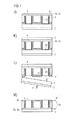
- FIG. 1 shows schematic sectional illustrations of a method for producing an optoelectronic semiconductor component 1 .
- a buffer layer 7 for instance formed from undoped GaN, is deposited on a growth substrate 2 , e.g. a sapphire substrate or a silicon substrate.
- FIG. 1B shows that islands 4 are deposited on the buffer layer 7 , for instance by self-organised, three-dimensional growth.
- the islands 4 preferably comprise a sacrificial layer 30 formed from an absorbing material, and an n-type layer 31 which is formed for example in the form of a hexagonal prism.
- the sacrificial layer 30 and the n-type layer 31 are preferably formed from the same material system, for instance from AlInGaN, in particular from GaN.
- the n-type layer 31 is n-doped and is a core of the islands 4 .
- An active zone 33 is epitaxially deposited on the n-type layer 31 , see FIG. 1C .
- the active zone 33 is based for example on InGaN.
- the active zone 33 surrounds the n-type layer 31 and the sacrificial layer 30 preferably all around, on a peripheral surface 40 and also on an upper side 46 facing away from the growth substrate 2 .
- a p-type layer 35 is deposited on the active zone 33 .
- the p-type layer 35 is p-doped and is preferably based on GaN or on AlGaN.
- a separating layer 5 is deposited on the grown islands 4 and on the buffer layer 7 over the whole area.
- the separating layer 5 is preferably formed of a material which has a smaller bandgap than the buffer layer 7 and the layers 31 , 35 .
- the material of the separating layer 5 is a material which can be etched selectively with respect to the materials of the islands 4 and of the buffer layer 7 , which has a coefficient of thermal expansion different from that of the materials of the islands 4 and of the buffer layer 7 , or which can be easily detached from the materials of the islands 4 and of the buffer layer 7 .
- these coefficients of thermal expansion differ from each other by at least a factor of 2 or 4 or 6 or 10.
- a transparent, electrical contact layer 8 a is deposited on the separating layer 5 .
- the contact layer 8 a is formed, for example, of indium tin oxide, ITO for short, and is a p-type contact.
- the contact layer 8 a is deposited directly on the p-type layer 35 on the peripheral surfaces 40 .
- a filling compound 9 is applied to the islands 4 and preferably also completely fills intermediate spaces between the islands 4 .
- the filling compound 9 is formed, for example, from an electrically insulating material such as silicon dioxide.
- the filling 9 , the contact layer 8 a and the semiconductor layer sequence 3 are partially removed so that the n-type layer 31 is exposed and the upper side 46 of the islands 4 facing away from the growth substrate 2 is produced.
- the side facing away from the growth substrate 2 and formed from the filling 9 and the islands 4 is, in the method step according to FIG. 1H , preferably planar and flat.
- FIG. 1I shows that a passivation 93 is applied to the active zone 33 .
- a transition between the p-type layer 35 and the n-type layer 31 can be protected against electrical short-circuits by the passivation 93 .
- Such a passivation 93 can be produced, for example, by a deactivation, in places, of the p-type layer 35 , in particular by a targeted destruction of the p-type conductive properties, e.g. by means of hydrogen plasma.
- the contact layer 8 b can also act as a mirror 96 and in this respect comprise, for example, a silver layer.
- the electrical contact layer 8 b can be formed by a layer stack formed by several, mutually different and in particular metallic layers.
- a carrier substrate 6 is applied to the electrical contact layer 8 b , e.g. by means of adhesion or soldering.
- a laser radiation R is used to remove the growth substrate 2 including the buffer layer 7 from the islands 4 and the filling 9 connecting the islands 4 .
- the laser radiation R is focussed on the separating layer 5 and on the sacrificial layer 30 .
- the sacrificial layer 30 and the separating layer 5 are partially destroyed and/or melted by the laser radiation R.
- the growth substrate 2 is preferably removed with the support of mechanical force effect.
- the separating layer and/or the sacrificial layer can be removed by means of a selective etching process and/or by bracing which is produced owing to a difference in the coefficients of thermal expansion of the separating layer 5 and of the buffer layer 7 .
- the separation of the growth substrate can likewise be supported by means of mechanical force effect, e.g. by ultrasound.
- FIG. 1M illustrates the produced semiconductor component 1 .
- electrical contact points 85 are attached.
- An electrical contacting of the n-type layer thus occurs via the electrical contact layer 8 b which can be formed as a mirror 96 and via the preferably transparent and radiolucent contact layer 8 a which is integrally formed on the islands 4 and surrounds the islands 4 all around, as viewed in a top view of the carrier substrate 6 .
- the electrical contact layer 8 b and the carrier substrate 6 can likewise be radiolucent.
- structuring or roughening can also optionally be formed on the islands 4 and/or on the filling 9 , for instance to improve light coupling-out efficiency.
- the n-type layer 31 can be partially removed.
- the islands 4 are grown on the growth substrate 2 in a self-organised manner, wherein the buffer layer 7 is optional.
- the individual islands 4 can have mutually different heights and/or diameters.
- the active zone 33 of the respective islands 4 can have a constant material composition and constant thickness, within manufacturing tolerances so that the different islands 4 have a substantially identical spectral directional characteristic.
- Such islands 4 as illustrated in FIG. 2A , can also be seen in FIG. 1 .
- a varying content of e.g. indium can be present over the active zone 33 so that a spectral broadband emission is possible.
- the islands 4 can be grown in a self-organised manner, wherein the n-type layer 31 , the active zone 33 and the p-type layer 35 of the semiconductor layer sequence 3 follow each other in the direction away from the growth substrate 2 , see FIG. 2B .
- the active zone 33 can thus be oriented substantially in parallel with the growth substrate 2 . If inclined facets, e.g. pyramid-shaped facets, are formed on a side of the n-type layer 31 facing away from the growth substrate 2 , then the active zone 33 can replicate a shape of these facets and be formed for example like a pyramid jacket.
- Islands 4 formed corresponding to FIGS. 2A and 2B can also be seen in FIGS. 2C and 2D .
- a masking layer 23 is applied in each case on the growth substrate 2 or on the optional buffer layer 7 .
- the islands 4 grow out of openings in the masking layer 23 . It is possible for the islands 4 to at least partially cover the masking layer 23 in each case, as viewed in a top view of the growth substrate 2 .
- FIGS. 2E and 2F A further option for producing the islands 4 is shown in conjunction with FIGS. 2E and 2F .
- a continuous, n-type layer 31 is produced on the growth substrate 2 or on the buffer layer 7 .
- This n-type layer 31 is then structured, for example by means of etching.
- the active zone 33 and the p-type layer 35 are grown on the resulting structures, see FIG. 2F .
- the further method steps can each be performed as shown in conjunction with FIG. 1 .
- the islands 4 can each be applied to the growth substrate 2 in a regular or irregular manner.
- the completed semiconductor component 1 has in each case, for example, at least 100 or at least 1000 or at least 10,000 islands 4 .
- a degree of coverage of the growth substrate 2 by the islands 4 also referred to as surface factor, amounts, as viewed in a top view, preferably to at least 5% or at least 25% or at least 50%. Alternatively or in addition, the surface factor amounts at the most to 90% or at the most to 80% or at the most to 75%.
- a surface of the active zone 33 in the direction perpendicular to the n-type layer 31 and to the p-type layer 35 , is, in particular in embodiments according to FIGS. 2A, 2C and 2F , preferably greater than a surface of the growth substrate 2 .
- the surface factor can thus be greater than 1, e.g. at least 1.5 or at least 3 or at least 5.
- FIGS. 3 to 7 each show sectional illustrations of variants of the design of the separating layer 5 .
- Corresponding separating layers 5 can also be used in methods as shown in conjunction with FIGS. 1 and 2 .
- the separating layer 5 is located directly on the growth substrate 2 .
- the growth substrate 2 is hereby reusable.
- the separating layer 5 is formed simultaneously as masking layer 23 and is located partially between the buffer layer 7 and the n-type layer 31 .
- the buffer layer 7 and the growth substrate 2 are removed.
- the masking layer 23 is accordingly at least partially destroyed by the laser radiation R.
- the separating layer 5 is applied to a side of the masking layer 23 facing away from the growth substrate 2 . It is hereby possible, see FIG. 5B , for the masking layer 23 to remain substantially uninfluenced by the laser radiation R on the growth substrate 2 . Therefore, the growth substrate 2 together with the masking layer 23 is reusable, e.g. after cleaning
- the at least partially destroyed, optional sacrificial layer 30 or, as a contrast to the illustration, the n-type layer 31 to copy the openings in the masking layer 23 .
- the separating layer 5 used as a marking layer 23 is attached directly to the growth substrate 2 .
- the masking layer 23 to which the separating layer 5 is attached, is located directly on the growth substrate 2 , as a contrast to the illustration in conjunction with FIG. 5 .
- FIG. 8 shows schematic sectional illustrations of further options of contacting the islands 4 , in each case prior to the detachment of the growth substrate 2 .
- the separating layer 5 , the masking layer 23 and the buffer layer 7 can each be configured as described in conjunction with FIGS. 1 to 7 .
- the p-type contacting occurs via the layer 8 a by means of the mirror 96 on the side facing the carrier substrate 6 .
- N-type contacting occurs via the side facing the growth substrate 2 .
- the side of the p-type layer 35 , facing away from the growth substrate 2 , and the active zone 33 are not removed according to FIG. 8A .
- the growth substrate 2 is preferably replaced by electrically conductive structures, not shown in FIG. 8A . The same applies for FIG. 8B .
- the upper side 46 of the n-type layer 31 is formed to a point and shaped into a pyramid e.g. by wet-chemical etching.
- the passivation 93 is located at a boundary between the upper side 46 and at the peripheral surfaces 40 .
- the filling 9 terminates substantially flush with the passivation 93 and does not extend, or only extends slightly, to the upper side 46 .
- the n-type layer 31 is hereby electrically contacted by the electrical contact layer 8 b on the carrier substrate 6 .
- the p-type layer 35 is formed via the radiolucent electrical contact layer 8 a which is integrally formed on the islands 4 .
- a separate passivation 93 is not formed, but rather a transition between the layers 31 , 35 and the active zone 33 are covered by the filling 9 in the direction away from the growth substrate 2 .
- the filling 9 thus partly covers the upper sides 46 of the n-type layer 31 and is introduced after the production of the upper sides 46 .
- the filling 9 can be introduced prior to the production of the upper sides 46 .
- the filling 9 can be applied in a single process step. Alternatively, the filling 9 can also be applied in several process steps, optionally interrupted by other process steps.
- FIG. 8E illustrates that the individual islands 4 can have different heights.
- Planarisation preferably occurs by way of the electrical contact layer 8 b which can be configured as a mirror 96 .
- the electrical contact layer 8 a for p-type contacting is preferably covered in a form-fitting manner by a thin passivation 93 a which copies a shape of the electrical contact layer 8 a .
- a further passivation 93 b is located at least in partial regions between the islands 4 , wherein the electrical contact layer 8 b for n-type contacting then follows said passivation in the direction away from the growth substrate 2 .
- FIG. 9 show exemplified embodiments of the semiconductor component 1 which have an in particular mechanically flexible carrier substrate 6 .
- the figures are illustrated rotated by 180° with respect to a growth direction of the semiconductor layer sequence 3 compared with FIGS. 1 to 8 .
- the carrier substrate 6 a via which the n-type contacting with the contact layer 8 b occurs, is a flexible substrate, e.g. a film based on a metal or a plastic.
- the contact layer 8 b is optionally configured as a mirror, as in all the other exemplified embodiments.
- a second, mechanically flexible carrier substrate 6 b is optionally attached to a side of the islands 4 facing away from the carrier substrate 6 a .
- the further carrier substrate 6 b is preferably radiolucent.
- the n-type layer 31 is contacted via the contact layer 8 b and the further carrier substrate 6 b .
- a corresponding contacting can be used for semiconductor components as shown in conjunction with FIG. 8A .
- the contact layers 8 a , 8 b are each connected to electrical contact points 85 for an electrical, external contacting of the semiconductor component 1 .
- the p-type contacting occurs via the contact layer 8 a which is integrally formed on the islands 4 .
- the n-type layer 31 is followed by a passivation 93 a which is attached to the former lower sides 42 facing the growth substrate.
- the electrical contact layer 8 a which can be composed of a layer formed prior to the removal of the growth substrate and of a layer formed after the removal of the growth substrate optionally protrudes into the further carrier 6 b according to FIG. 9C .
- the further carrier 6 b can be applied to the filler 9 and to the islands 4 as a coating.
- the side of the carrier 6 b facing the islands 4 may be flat.
- FIG. 9D illustrates an electrical contacting for the islands 4 , as shown in conjunction with FIG. 8 b.
- FIGS. 10 to 12 show sectional illustrations—in the case of the figures marked ‘A’—and schematic top views—in the case of the figures marked ‘B’—of the optoelectronic semiconductor component 1 .
- the electrical contacting is designed as explained in conjunction with FIG. 9C .
- all the other illustrated types of contacting and designs of the contact layers 8 a , 8 b can be used in conjunction with FIGS. 10 to 12 .
- the contacting layers 8 a , 8 b are each continuous layers. All the islands 4 are thus connected electrically in parallel and can be electrically actuated together.
- FIG. 11 illustrates that the electrical contact layers 8 a , 8 b are located on mutually opposite sides of the islands 4 and are each configured in a strip-like manner, wherein the strips are oriented orthogonal to one another. In this manner, the individual islands 4 can be electrically actuated individually.
- Each of the adjacent path-like contact layers 8 a , 8 b contacts a row or a column of the islands 4 , see FIG. 11B . In a deviation therefrom, it is possible for the individual paths to contact several rows and columns of the islands 4 together.
- FIG. 12 illustrates that the contact layers 8 a , 8 b are each restricted to individual islands 4 .
- a customised interconnection of the islands 4 e.g. on an external mounting structure, not shown, is possible.
- several islands 4 can be covered by contiguous contact layers 8 a , 8 b , which means that groups of islands 4 can be electrically switched together.
- Conductor paths, not shown, can be attached between the contact layers 8 a , 8 b located directly on the islands 4 in order to form a more complex interconnection of the islands 4 .
- FIGS. 13A and 13B show that the p-type contact layer 8 a is arranged spaced apart from the separating layer 5 .
- a first filler 9 a is located between the separating layer 5 and the contact layer 8 a .
- the contact layer 8 a is thus embedded in the fillers 9 a , 9 b together with the passivation 93 . It is hereby possible for only one part of the active zone 33 to be supplied with current.
Landscapes
- Engineering & Computer Science (AREA)
- Power Engineering (AREA)
- Computer Hardware Design (AREA)
- Microelectronics & Electronic Packaging (AREA)
- Manufacturing & Machinery (AREA)
- Physics & Mathematics (AREA)
- Condensed Matter Physics & Semiconductors (AREA)
- General Physics & Mathematics (AREA)
- Led Devices (AREA)
Abstract
Description
B) producing one or several separating layers on a side of the islands facing the growth substrate, wherein the at least one separating layer surrounds the islands all around, as viewed in a top view of the growth substrate,
C) attaching a carrier substrate to a side of the islands facing away from the growth substrate, and
D) detaching the growth substrate from the islands, for instance by means of radiation, wherein, during the detachment, at least a part of the separating layer is destroyed and/or at least temporarily softened, for instance by the laser radiation.
Claims (17)
Applications Claiming Priority (4)
| Application Number | Priority Date | Filing Date | Title |
|---|---|---|---|
| DE102012109594 | 2012-10-09 | ||
| DE102012109594.9A DE102012109594A1 (en) | 2012-10-09 | 2012-10-09 | Method for producing an optoelectronic semiconductor component and optoelectronic semiconductor component |
| DE102012109594.9 | 2012-10-09 | ||
| PCT/EP2013/070449 WO2014056762A2 (en) | 2012-10-09 | 2013-10-01 | Method for producing an optoelectronic semiconductor component and optoelectronic semiconductor component |
Publications (2)
| Publication Number | Publication Date |
|---|---|
| US20150279903A1 US20150279903A1 (en) | 2015-10-01 |
| US9691815B2 true US9691815B2 (en) | 2017-06-27 |
Family
ID=49274654
Family Applications (1)
| Application Number | Title | Priority Date | Filing Date |
|---|---|---|---|
| US14/434,760 Active US9691815B2 (en) | 2012-10-09 | 2013-10-01 | Method for producing an optoelectronic semiconductor component, and optoelectronic semiconductor component |
Country Status (3)
| Country | Link |
|---|---|
| US (1) | US9691815B2 (en) |
| DE (1) | DE102012109594A1 (en) |
| WO (1) | WO2014056762A2 (en) |
Families Citing this family (8)
| Publication number | Priority date | Publication date | Assignee | Title |
|---|---|---|---|---|
| DE102013211707B4 (en) * | 2013-06-20 | 2024-03-28 | OSRAM Opto Semiconductors Gesellschaft mit beschränkter Haftung | Single support array, multiple array array and method of making an array |
| DE102014116276A1 (en) * | 2014-11-07 | 2016-05-12 | Osram Opto Semiconductors Gmbh | An epitaxial wafer, device and method of making an epitaxial wafer and a device |
| FR3053531B1 (en) * | 2016-06-30 | 2018-08-17 | Aledia | OPTOELECTRONIC DEVICE WITH THREE DIMENSIONAL DIODES |
| DE102016112857A1 (en) | 2016-07-13 | 2018-01-18 | Osram Opto Semiconductors Gmbh | Optoelectronic semiconductor chip and method for producing an optoelectronic semiconductor chip |
| JP2020534687A (en) | 2017-09-15 | 2020-11-26 | ザ リージェンツ オブ ザ ユニバーシティ オブ カリフォルニア | How to remove the substrate using cleavage technique |
| FR3076078B1 (en) * | 2017-12-27 | 2021-11-26 | Aledia | OPTOELECTRONIC DEVICE WITH THREE-DIMENSIONAL DIODE MATRIX |
| KR20210000351A (en) | 2019-06-24 | 2021-01-05 | 삼성전자주식회사 | Semiconductor light emitting diode and display apparatus |
| FR3105878B1 (en) * | 2019-12-26 | 2023-10-27 | Aledia | Device with three-dimensional optoelectronic components for laser cutting and method for laser cutting of such a device |
Citations (14)
| Publication number | Priority date | Publication date | Assignee | Title |
|---|---|---|---|---|
| US20060131679A1 (en) | 2004-12-20 | 2006-06-22 | Palo Alto Research Center Incorporated | Systems and methods for electrical contacts to arrays of vertically aligned nanorods |
| US20080036038A1 (en) | 2006-03-10 | 2008-02-14 | Hersee Stephen D | PULSED GROWTH OF CATALYST-FREE GROWITH OF GaN NANOWIRES AND APPLICATION IN GROUP III NITRIDE SEMICONDUCTOR BULK MATERIAL |
| WO2008129859A1 (en) | 2007-04-13 | 2008-10-30 | Panasonic Corporation | Light-emitting element and display device |
| US20100117997A1 (en) | 2007-03-08 | 2010-05-13 | Haase Michael A | Array of luminescent elements |
| WO2010059131A1 (en) | 2008-11-19 | 2010-05-27 | Agency For Science, Technology And Research | Method of at least partially releasing an epitaxial layer |
| US20100327258A1 (en) | 2007-07-05 | 2010-12-30 | Samsung Electronics Co., Ltd. | Method for producing core-shell nanowires, nanowires produced by the method and nanowire device comprising the nanowires |
| US20110095260A1 (en) * | 2009-10-28 | 2011-04-28 | Samsung Electronics Co., Ltd. | Light emitting device |
| US20110151602A1 (en) | 2009-12-18 | 2011-06-23 | Cooledge Lighting, Inc. | Method of manufacturing transferable elements incorporating radiation enabled lift off for allowing transfer from host substrate |
| DE102010012711A1 (en) | 2010-03-25 | 2011-09-29 | Osram Opto Semiconductors Gmbh | A radiation-emitting semiconductor component and method for producing a radiation-emitting semiconductor component |
| WO2011123257A1 (en) | 2010-03-30 | 2011-10-06 | Eastman Kodak Company | Light emitting nanowire device |
| US20110297913A1 (en) | 2010-06-08 | 2011-12-08 | Sundiode Inc. | Nanostructure optoelectronic device having sidewall electrical contact |
| US20110298001A1 (en) | 2010-06-03 | 2011-12-08 | Kabushiki Kaisha Toshiba | Method for manufacturing light-emitting device and light-emitting device manufactured by the same |
| WO2011162715A1 (en) | 2010-06-24 | 2011-12-29 | Glo Ab | Substrate with buffer layer for oriented nanowire growth |
| DE102012101718A1 (en) | 2012-03-01 | 2013-09-05 | Osram Opto Semiconductors Gmbh | Optoelectronic semiconductor chip |
-
2012
- 2012-10-09 DE DE102012109594.9A patent/DE102012109594A1/en active Pending
-
2013
- 2013-10-01 US US14/434,760 patent/US9691815B2/en active Active
- 2013-10-01 WO PCT/EP2013/070449 patent/WO2014056762A2/en active Application Filing
Patent Citations (15)
| Publication number | Priority date | Publication date | Assignee | Title |
|---|---|---|---|---|
| US20060131679A1 (en) | 2004-12-20 | 2006-06-22 | Palo Alto Research Center Incorporated | Systems and methods for electrical contacts to arrays of vertically aligned nanorods |
| US20080036038A1 (en) | 2006-03-10 | 2008-02-14 | Hersee Stephen D | PULSED GROWTH OF CATALYST-FREE GROWITH OF GaN NANOWIRES AND APPLICATION IN GROUP III NITRIDE SEMICONDUCTOR BULK MATERIAL |
| US20100117997A1 (en) | 2007-03-08 | 2010-05-13 | Haase Michael A | Array of luminescent elements |
| WO2008129859A1 (en) | 2007-04-13 | 2008-10-30 | Panasonic Corporation | Light-emitting element and display device |
| US20100327258A1 (en) | 2007-07-05 | 2010-12-30 | Samsung Electronics Co., Ltd. | Method for producing core-shell nanowires, nanowires produced by the method and nanowire device comprising the nanowires |
| WO2010059131A1 (en) | 2008-11-19 | 2010-05-27 | Agency For Science, Technology And Research | Method of at least partially releasing an epitaxial layer |
| US20110095260A1 (en) * | 2009-10-28 | 2011-04-28 | Samsung Electronics Co., Ltd. | Light emitting device |
| US20110151602A1 (en) | 2009-12-18 | 2011-06-23 | Cooledge Lighting, Inc. | Method of manufacturing transferable elements incorporating radiation enabled lift off for allowing transfer from host substrate |
| DE102010012711A1 (en) | 2010-03-25 | 2011-09-29 | Osram Opto Semiconductors Gmbh | A radiation-emitting semiconductor component and method for producing a radiation-emitting semiconductor component |
| WO2011117056A1 (en) | 2010-03-25 | 2011-09-29 | Osram Opto Semiconductors Gmbh | Radiation-emitting semiconductor component and method for producing a radiation-emitting semiconductor component |
| WO2011123257A1 (en) | 2010-03-30 | 2011-10-06 | Eastman Kodak Company | Light emitting nanowire device |
| US20110298001A1 (en) | 2010-06-03 | 2011-12-08 | Kabushiki Kaisha Toshiba | Method for manufacturing light-emitting device and light-emitting device manufactured by the same |
| US20110297913A1 (en) | 2010-06-08 | 2011-12-08 | Sundiode Inc. | Nanostructure optoelectronic device having sidewall electrical contact |
| WO2011162715A1 (en) | 2010-06-24 | 2011-12-29 | Glo Ab | Substrate with buffer layer for oriented nanowire growth |
| DE102012101718A1 (en) | 2012-03-01 | 2013-09-05 | Osram Opto Semiconductors Gmbh | Optoelectronic semiconductor chip |
Non-Patent Citations (2)
| Title |
|---|
| Ky, J.: "Closer to Flexible LED Displays", <http://www.yalescientific.org/2010/05/closer-to-flexible-led-displays/>, May 12, 2011, pp. 1-3. |
| Lee, S. et al.: "Water-resistant flexible GaN LED on a liquid crystal polymer substrate for implantable biomedical applications"; Elsevier, Nano Energy, vol. 1, 2012, pp. 145-151. |
Also Published As
| Publication number | Publication date |
|---|---|
| WO2014056762A3 (en) | 2014-06-19 |
| WO2014056762A2 (en) | 2014-04-17 |
| DE102012109594A1 (en) | 2014-04-10 |
| US20150279903A1 (en) | 2015-10-01 |
Similar Documents
| Publication | Publication Date | Title |
|---|---|---|
| US9691815B2 (en) | Method for producing an optoelectronic semiconductor component, and optoelectronic semiconductor component | |
| KR100867541B1 (en) | Method of manufacturing vertical light emitting device | |
| US8242530B2 (en) | Light emitting device and method for fabricating the same | |
| KR102231083B1 (en) | Method of separating light emitting devices formed on a substrate wafer | |
| TWI559573B (en) | Light emitting diode | |
| US20140246647A1 (en) | Nanostructure light emitting device and method of manufacturing the same | |
| US8420439B2 (en) | Method of producing a radiation-emitting thin film component and radiation-emitting thin film component | |
| EP2761678A2 (en) | Nanowire sized opto-electronic structure and method for manufacturing the same | |
| KR102471670B1 (en) | High power light emitting diode and light emitting module having the same | |
| JP2006135321A (en) | Light emitting device and method of manufacturing the same | |
| KR100649763B1 (en) | A method of producing vertical nitride light emitting devices | |
| US9514926B2 (en) | Substrate recycling method | |
| KR20110077707A (en) | Vertical light emitting diode and manufacturing method of the same | |
| US9966498B2 (en) | Method for manufacturing light-emitting element | |
| EP2426741B1 (en) | Method of fabricating a semiconductor light emitting device | |
| KR20140068474A (en) | Method for separating substrate and method for fabricating light-emitting diode chip using the same | |
| KR101969308B1 (en) | Semiconductor light emitting device and manufacturing method of the same | |
| US20230290806A1 (en) | Led device and method of manufacture | |
| US20230048093A1 (en) | Micro-led and method of manufacture | |
| JP4890419B2 (en) | Nitride semiconductor light emitting device and manufacturing method | |
| KR20140074040A (en) | Light emitting diode and method for fabricating the same | |
| JP2019212834A (en) | Light-emitting element and method of manufacturing the same | |
| KR20140123318A (en) | Method for separating growth substrate using stress and method for fabricating semiconductor device using the same | |
| KR20130110380A (en) | Semiconductor light emitting device and manufacturing method of the same | |
| KR20150048474A (en) | Method of separating substrate and method of fabricating semiconductor device using the same |
Legal Events
| Date | Code | Title | Description |
|---|---|---|---|
| AS | Assignment |
Owner name: OSRAM OPTO SEMICONDUCTORS GMBH, GERMANY Free format text: ASSIGNMENT OF ASSIGNORS INTEREST;ASSIGNORS:MANDL, MARTIN;STRASSBERG, MARTIN;KOELPER, CHRISTOPHER;AND OTHERS;SIGNING DATES FROM 20150609 TO 20150622;REEL/FRAME:038346/0065 |
|
| AS | Assignment |
Owner name: OSRAM OPTO SEMICONDUCTORS GMBH, GERMANY Free format text: CORRECTIVE ASSIGNMENT TO CORRECT THE SECOND INVENTOR NAME PREVIOUSLY RECORDED AT REEL: 038346 FRAME: 0065. ASSIGNOR(S) HEREBY CONFIRMS THE ASSIGNMENT;ASSIGNORS:MANDL, MARTIN;STRASSBURG, MARTIN;KOELPER, CHRISTOPHER;AND OTHERS;SIGNING DATES FROM 20150609 TO 20150622;REEL/FRAME:042570/0233 |
|
| STCF | Information on status: patent grant |
Free format text: PATENTED CASE |
|
| AS | Assignment |
Owner name: OSRAM OLED GMBH, GERMANY Free format text: ASSIGNMENT OF ASSIGNORS INTEREST;ASSIGNOR:OSRAM OPTO SEMICONDUCTORS GMBH;REEL/FRAME:051467/0906 Effective date: 20191218 |
|
| MAFP | Maintenance fee payment |
Free format text: PAYMENT OF MAINTENANCE FEE, 4TH YEAR, LARGE ENTITY (ORIGINAL EVENT CODE: M1551); ENTITY STATUS OF PATENT OWNER: LARGE ENTITY Year of fee payment: 4 |