US9620578B2 - Array substrate, manufacture method thereof, and display panel - Google Patents
Array substrate, manufacture method thereof, and display panel Download PDFInfo
- Publication number
- US9620578B2 US9620578B2 US14/436,517 US201414436517A US9620578B2 US 9620578 B2 US9620578 B2 US 9620578B2 US 201414436517 A US201414436517 A US 201414436517A US 9620578 B2 US9620578 B2 US 9620578B2
- Authority
- US
- United States
- Prior art keywords
- layer
- electrode
- solar cell
- gate
- cell structure
- Prior art date
- Legal status (The legal status is an assumption and is not a legal conclusion. Google has not performed a legal analysis and makes no representation as to the accuracy of the status listed.)
- Active
Links
- 239000000758 substrate Substances 0.000 title claims abstract description 96
- 238000000034 method Methods 0.000 title claims abstract description 59
- 238000004519 manufacturing process Methods 0.000 title claims abstract description 38
- 239000010409 thin film Substances 0.000 claims abstract description 6
- 230000004888 barrier function Effects 0.000 claims description 44
- 239000000463 material Substances 0.000 claims description 39
- 239000002210 silicon-based material Substances 0.000 claims description 36
- 238000002161 passivation Methods 0.000 claims description 17
- 239000011159 matrix material Substances 0.000 claims description 3
- 238000005516 engineering process Methods 0.000 abstract description 8
- 230000008569 process Effects 0.000 description 34
- 238000000059 patterning Methods 0.000 description 21
- 238000000151 deposition Methods 0.000 description 19
- 229910052751 metal Inorganic materials 0.000 description 14
- 239000002184 metal Substances 0.000 description 14
- 239000010408 film Substances 0.000 description 11
- 229910052581 Si3N4 Inorganic materials 0.000 description 8
- VYPSYNLAJGMNEJ-UHFFFAOYSA-N Silicium dioxide Chemical compound O=[Si]=O VYPSYNLAJGMNEJ-UHFFFAOYSA-N 0.000 description 8
- 239000004020 conductor Substances 0.000 description 8
- HQVNEWCFYHHQES-UHFFFAOYSA-N silicon nitride Chemical compound N12[Si]34N5[Si]62N3[Si]51N64 HQVNEWCFYHHQES-UHFFFAOYSA-N 0.000 description 8
- 229910052814 silicon oxide Inorganic materials 0.000 description 8
- 230000005525 hole transport Effects 0.000 description 6
- 239000004065 semiconductor Substances 0.000 description 6
- 229910045601 alloy Inorganic materials 0.000 description 5
- 239000000956 alloy Substances 0.000 description 5
- 239000011651 chromium Substances 0.000 description 5
- 239000010949 copper Substances 0.000 description 5
- 239000010936 titanium Substances 0.000 description 5
- XLOMVQKBTHCTTD-UHFFFAOYSA-N Zinc monoxide Chemical compound [Zn]=O XLOMVQKBTHCTTD-UHFFFAOYSA-N 0.000 description 4
- 229910052782 aluminium Inorganic materials 0.000 description 4
- 229910052804 chromium Inorganic materials 0.000 description 4
- 229910052802 copper Inorganic materials 0.000 description 4
- 229910052750 molybdenum Inorganic materials 0.000 description 4
- 229910052719 titanium Inorganic materials 0.000 description 4
- 229910052721 tungsten Inorganic materials 0.000 description 4
- 230000005284 excitation Effects 0.000 description 3
- 230000005283 ground state Effects 0.000 description 3
- 239000011810 insulating material Substances 0.000 description 3
- 230000000149 penetrating effect Effects 0.000 description 3
- 229910021420 polycrystalline silicon Inorganic materials 0.000 description 3
- 229910052715 tantalum Inorganic materials 0.000 description 3
- 230000007704 transition Effects 0.000 description 3
- GYHNNYVSQQEPJS-UHFFFAOYSA-N Gallium Chemical compound [Ga] GYHNNYVSQQEPJS-UHFFFAOYSA-N 0.000 description 2
- XEEYBQQBJWHFJM-UHFFFAOYSA-N Iron Chemical compound [Fe] XEEYBQQBJWHFJM-UHFFFAOYSA-N 0.000 description 2
- 229910021417 amorphous silicon Inorganic materials 0.000 description 2
- 230000008901 benefit Effects 0.000 description 2
- 238000011161 development Methods 0.000 description 2
- 238000010586 diagram Methods 0.000 description 2
- 229910052733 gallium Inorganic materials 0.000 description 2
- 229910052738 indium Inorganic materials 0.000 description 2
- APFVFJFRJDLVQX-UHFFFAOYSA-N indium atom Chemical compound [In] APFVFJFRJDLVQX-UHFFFAOYSA-N 0.000 description 2
- AMGQUBHHOARCQH-UHFFFAOYSA-N indium;oxotin Chemical compound [In].[Sn]=O AMGQUBHHOARCQH-UHFFFAOYSA-N 0.000 description 2
- 238000001755 magnetron sputter deposition Methods 0.000 description 2
- 238000012986 modification Methods 0.000 description 2
- 230000004048 modification Effects 0.000 description 2
- -1 or the like Substances 0.000 description 2
- 239000000243 solution Substances 0.000 description 2
- 238000012546 transfer Methods 0.000 description 2
- 229910000314 transition metal oxide Inorganic materials 0.000 description 2
- 238000002834 transmittance Methods 0.000 description 2
- 239000011787 zinc oxide Substances 0.000 description 2
- VYZAMTAEIAYCRO-UHFFFAOYSA-N Chromium Chemical compound [Cr] VYZAMTAEIAYCRO-UHFFFAOYSA-N 0.000 description 1
- RYGMFSIKBFXOCR-UHFFFAOYSA-N Copper Chemical compound [Cu] RYGMFSIKBFXOCR-UHFFFAOYSA-N 0.000 description 1
- ZOKXTWBITQBERF-UHFFFAOYSA-N Molybdenum Chemical compound [Mo] ZOKXTWBITQBERF-UHFFFAOYSA-N 0.000 description 1
- RTAQQCXQSZGOHL-UHFFFAOYSA-N Titanium Chemical compound [Ti] RTAQQCXQSZGOHL-UHFFFAOYSA-N 0.000 description 1
- XAGFODPZIPBFFR-UHFFFAOYSA-N aluminium Chemical compound [Al] XAGFODPZIPBFFR-UHFFFAOYSA-N 0.000 description 1
- 230000008859 change Effects 0.000 description 1
- 239000011248 coating agent Substances 0.000 description 1
- 238000000576 coating method Methods 0.000 description 1
- 238000013461 design Methods 0.000 description 1
- 239000011521 glass Substances 0.000 description 1
- 238000002347 injection Methods 0.000 description 1
- 239000007924 injection Substances 0.000 description 1
- 229910052742 iron Inorganic materials 0.000 description 1
- 239000004973 liquid crystal related substance Substances 0.000 description 1
- 239000007769 metal material Substances 0.000 description 1
- 229910044991 metal oxide Inorganic materials 0.000 description 1
- 150000004706 metal oxides Chemical class 0.000 description 1
- 239000011733 molybdenum Substances 0.000 description 1
- 229910021421 monocrystalline silicon Inorganic materials 0.000 description 1
- 238000013082 photovoltaic technology Methods 0.000 description 1
- 238000010248 power generation Methods 0.000 description 1
- WFKWXMTUELFFGS-UHFFFAOYSA-N tungsten Chemical compound [W] WFKWXMTUELFFGS-UHFFFAOYSA-N 0.000 description 1
- 239000010937 tungsten Substances 0.000 description 1
- 230000007306 turnover Effects 0.000 description 1
Images


Classifications
-
- H01L27/3276—
-
- H—ELECTRICITY
- H10—SEMICONDUCTOR DEVICES; ELECTRIC SOLID-STATE DEVICES NOT OTHERWISE PROVIDED FOR
- H10K—ORGANIC ELECTRIC SOLID-STATE DEVICES
- H10K59/00—Integrated devices, or assemblies of multiple devices, comprising at least one organic light-emitting element covered by group H10K50/00
- H10K59/10—OLED displays
- H10K59/12—Active-matrix OLED [AMOLED] displays
- H10K59/131—Interconnections, e.g. wiring lines or terminals
-
- H—ELECTRICITY
- H01—ELECTRIC ELEMENTS
- H01L—SEMICONDUCTOR DEVICES NOT COVERED BY CLASS H10
- H01L27/00—Devices consisting of a plurality of semiconductor or other solid-state components formed in or on a common substrate
- H01L27/02—Devices consisting of a plurality of semiconductor or other solid-state components formed in or on a common substrate including semiconductor components specially adapted for rectifying, oscillating, amplifying or switching and having potential barriers; including integrated passive circuit elements having potential barriers
- H01L27/12—Devices consisting of a plurality of semiconductor or other solid-state components formed in or on a common substrate including semiconductor components specially adapted for rectifying, oscillating, amplifying or switching and having potential barriers; including integrated passive circuit elements having potential barriers the substrate being other than a semiconductor body, e.g. an insulating body
- H01L27/1214—Devices consisting of a plurality of semiconductor or other solid-state components formed in or on a common substrate including semiconductor components specially adapted for rectifying, oscillating, amplifying or switching and having potential barriers; including integrated passive circuit elements having potential barriers the substrate being other than a semiconductor body, e.g. an insulating body comprising a plurality of TFTs formed on a non-semiconducting substrate, e.g. driving circuits for AMLCDs
- H01L27/1248—Devices consisting of a plurality of semiconductor or other solid-state components formed in or on a common substrate including semiconductor components specially adapted for rectifying, oscillating, amplifying or switching and having potential barriers; including integrated passive circuit elements having potential barriers the substrate being other than a semiconductor body, e.g. an insulating body comprising a plurality of TFTs formed on a non-semiconducting substrate, e.g. driving circuits for AMLCDs with a particular composition or shape of the interlayer dielectric specially adapted to the circuit arrangement
-
- H—ELECTRICITY
- H01—ELECTRIC ELEMENTS
- H01L—SEMICONDUCTOR DEVICES NOT COVERED BY CLASS H10
- H01L27/00—Devices consisting of a plurality of semiconductor or other solid-state components formed in or on a common substrate
- H01L27/02—Devices consisting of a plurality of semiconductor or other solid-state components formed in or on a common substrate including semiconductor components specially adapted for rectifying, oscillating, amplifying or switching and having potential barriers; including integrated passive circuit elements having potential barriers
- H01L27/12—Devices consisting of a plurality of semiconductor or other solid-state components formed in or on a common substrate including semiconductor components specially adapted for rectifying, oscillating, amplifying or switching and having potential barriers; including integrated passive circuit elements having potential barriers the substrate being other than a semiconductor body, e.g. an insulating body
- H01L27/1214—Devices consisting of a plurality of semiconductor or other solid-state components formed in or on a common substrate including semiconductor components specially adapted for rectifying, oscillating, amplifying or switching and having potential barriers; including integrated passive circuit elements having potential barriers the substrate being other than a semiconductor body, e.g. an insulating body comprising a plurality of TFTs formed on a non-semiconducting substrate, e.g. driving circuits for AMLCDs
- H01L27/1259—Multistep manufacturing methods
-
- H01L27/3227—
-
- H01L27/3258—
-
- H01L27/3262—
-
- H—ELECTRICITY
- H01—ELECTRIC ELEMENTS
- H01L—SEMICONDUCTOR DEVICES NOT COVERED BY CLASS H10
- H01L29/00—Semiconductor devices specially adapted for rectifying, amplifying, oscillating or switching and having potential barriers; Capacitors or resistors having potential barriers, e.g. a PN-junction depletion layer or carrier concentration layer; Details of semiconductor bodies or of electrodes thereof ; Multistep manufacturing processes therefor
- H01L29/40—Electrodes ; Multistep manufacturing processes therefor
- H01L29/41—Electrodes ; Multistep manufacturing processes therefor characterised by their shape, relative sizes or dispositions
- H01L29/417—Electrodes ; Multistep manufacturing processes therefor characterised by their shape, relative sizes or dispositions carrying the current to be rectified, amplified or switched
- H01L29/41725—Source or drain electrodes for field effect devices
- H01L29/41733—Source or drain electrodes for field effect devices for thin film transistors with insulated gate
-
- H—ELECTRICITY
- H01—ELECTRIC ELEMENTS
- H01L—SEMICONDUCTOR DEVICES NOT COVERED BY CLASS H10
- H01L29/00—Semiconductor devices specially adapted for rectifying, amplifying, oscillating or switching and having potential barriers; Capacitors or resistors having potential barriers, e.g. a PN-junction depletion layer or carrier concentration layer; Details of semiconductor bodies or of electrodes thereof ; Multistep manufacturing processes therefor
- H01L29/66—Types of semiconductor device ; Multistep manufacturing processes therefor
- H01L29/68—Types of semiconductor device ; Multistep manufacturing processes therefor controllable by only the electric current supplied, or only the electric potential applied, to an electrode which does not carry the current to be rectified, amplified or switched
- H01L29/76—Unipolar devices, e.g. field effect transistors
- H01L29/772—Field effect transistors
- H01L29/78—Field effect transistors with field effect produced by an insulated gate
- H01L29/786—Thin film transistors, i.e. transistors with a channel being at least partly a thin film
- H01L29/78696—Thin film transistors, i.e. transistors with a channel being at least partly a thin film characterised by the structure of the channel, e.g. multichannel, transverse or longitudinal shape, length or width, doping structure, or the overlap or alignment between the channel and the gate, the source or the drain, or the contacting structure of the channel
-
- H—ELECTRICITY
- H01—ELECTRIC ELEMENTS
- H01L—SEMICONDUCTOR DEVICES NOT COVERED BY CLASS H10
- H01L31/00—Semiconductor devices sensitive to infrared radiation, light, electromagnetic radiation of shorter wavelength or corpuscular radiation and specially adapted either for the conversion of the energy of such radiation into electrical energy or for the control of electrical energy by such radiation; Processes or apparatus specially adapted for the manufacture or treatment thereof or of parts thereof; Details thereof
- H01L31/0248—Semiconductor devices sensitive to infrared radiation, light, electromagnetic radiation of shorter wavelength or corpuscular radiation and specially adapted either for the conversion of the energy of such radiation into electrical energy or for the control of electrical energy by such radiation; Processes or apparatus specially adapted for the manufacture or treatment thereof or of parts thereof; Details thereof characterised by their semiconductor bodies
- H01L31/0256—Semiconductor devices sensitive to infrared radiation, light, electromagnetic radiation of shorter wavelength or corpuscular radiation and specially adapted either for the conversion of the energy of such radiation into electrical energy or for the control of electrical energy by such radiation; Processes or apparatus specially adapted for the manufacture or treatment thereof or of parts thereof; Details thereof characterised by their semiconductor bodies characterised by the material
- H01L31/0264—Inorganic materials
- H01L31/028—Inorganic materials including, apart from doping material or other impurities, only elements of Group IV of the Periodic Table
-
- H—ELECTRICITY
- H01—ELECTRIC ELEMENTS
- H01L—SEMICONDUCTOR DEVICES NOT COVERED BY CLASS H10
- H01L31/00—Semiconductor devices sensitive to infrared radiation, light, electromagnetic radiation of shorter wavelength or corpuscular radiation and specially adapted either for the conversion of the energy of such radiation into electrical energy or for the control of electrical energy by such radiation; Processes or apparatus specially adapted for the manufacture or treatment thereof or of parts thereof; Details thereof
- H01L31/04—Semiconductor devices sensitive to infrared radiation, light, electromagnetic radiation of shorter wavelength or corpuscular radiation and specially adapted either for the conversion of the energy of such radiation into electrical energy or for the control of electrical energy by such radiation; Processes or apparatus specially adapted for the manufacture or treatment thereof or of parts thereof; Details thereof adapted as photovoltaic [PV] conversion devices
- H01L31/06—Semiconductor devices sensitive to infrared radiation, light, electromagnetic radiation of shorter wavelength or corpuscular radiation and specially adapted either for the conversion of the energy of such radiation into electrical energy or for the control of electrical energy by such radiation; Processes or apparatus specially adapted for the manufacture or treatment thereof or of parts thereof; Details thereof adapted as photovoltaic [PV] conversion devices characterised by potential barriers
- H01L31/075—Semiconductor devices sensitive to infrared radiation, light, electromagnetic radiation of shorter wavelength or corpuscular radiation and specially adapted either for the conversion of the energy of such radiation into electrical energy or for the control of electrical energy by such radiation; Processes or apparatus specially adapted for the manufacture or treatment thereof or of parts thereof; Details thereof adapted as photovoltaic [PV] conversion devices characterised by potential barriers the potential barriers being only of the PIN type, e.g. amorphous silicon PIN solar cells
-
- H—ELECTRICITY
- H01—ELECTRIC ELEMENTS
- H01L—SEMICONDUCTOR DEVICES NOT COVERED BY CLASS H10
- H01L31/00—Semiconductor devices sensitive to infrared radiation, light, electromagnetic radiation of shorter wavelength or corpuscular radiation and specially adapted either for the conversion of the energy of such radiation into electrical energy or for the control of electrical energy by such radiation; Processes or apparatus specially adapted for the manufacture or treatment thereof or of parts thereof; Details thereof
- H01L31/18—Processes or apparatus specially adapted for the manufacture or treatment of these devices or of parts thereof
- H01L31/1804—Processes or apparatus specially adapted for the manufacture or treatment of these devices or of parts thereof comprising only elements of Group IV of the Periodic Table
-
- H01L51/56—
-
- H—ELECTRICITY
- H10—SEMICONDUCTOR DEVICES; ELECTRIC SOLID-STATE DEVICES NOT OTHERWISE PROVIDED FOR
- H10K—ORGANIC ELECTRIC SOLID-STATE DEVICES
- H10K59/00—Integrated devices, or assemblies of multiple devices, comprising at least one organic light-emitting element covered by group H10K50/00
- H10K59/10—OLED displays
- H10K59/12—Active-matrix OLED [AMOLED] displays
- H10K59/121—Active-matrix OLED [AMOLED] displays characterised by the geometry or disposition of pixel elements
- H10K59/1213—Active-matrix OLED [AMOLED] displays characterised by the geometry or disposition of pixel elements the pixel elements being TFTs
-
- H—ELECTRICITY
- H10—SEMICONDUCTOR DEVICES; ELECTRIC SOLID-STATE DEVICES NOT OTHERWISE PROVIDED FOR
- H10K—ORGANIC ELECTRIC SOLID-STATE DEVICES
- H10K59/00—Integrated devices, or assemblies of multiple devices, comprising at least one organic light-emitting element covered by group H10K50/00
- H10K59/10—OLED displays
- H10K59/12—Active-matrix OLED [AMOLED] displays
- H10K59/124—Insulating layers formed between TFT elements and OLED elements
-
- H—ELECTRICITY
- H10—SEMICONDUCTOR DEVICES; ELECTRIC SOLID-STATE DEVICES NOT OTHERWISE PROVIDED FOR
- H10K—ORGANIC ELECTRIC SOLID-STATE DEVICES
- H10K59/00—Integrated devices, or assemblies of multiple devices, comprising at least one organic light-emitting element covered by group H10K50/00
- H10K59/60—OLEDs integrated with inorganic light-sensitive elements, e.g. with inorganic solar cells or inorganic photodiodes
-
- H—ELECTRICITY
- H10—SEMICONDUCTOR DEVICES; ELECTRIC SOLID-STATE DEVICES NOT OTHERWISE PROVIDED FOR
- H10K—ORGANIC ELECTRIC SOLID-STATE DEVICES
- H10K71/00—Manufacture or treatment specially adapted for the organic devices covered by this subclass
-
- H01L2227/323—
-
- H—ELECTRICITY
- H10—SEMICONDUCTOR DEVICES; ELECTRIC SOLID-STATE DEVICES NOT OTHERWISE PROVIDED FOR
- H10K—ORGANIC ELECTRIC SOLID-STATE DEVICES
- H10K59/00—Integrated devices, or assemblies of multiple devices, comprising at least one organic light-emitting element covered by group H10K50/00
- H10K59/10—OLED displays
- H10K59/12—Active-matrix OLED [AMOLED] displays
- H10K59/1201—Manufacture or treatment
-
- H—ELECTRICITY
- H10—SEMICONDUCTOR DEVICES; ELECTRIC SOLID-STATE DEVICES NOT OTHERWISE PROVIDED FOR
- H10K—ORGANIC ELECTRIC SOLID-STATE DEVICES
- H10K71/00—Manufacture or treatment specially adapted for the organic devices covered by this subclass
- H10K71/20—Changing the shape of the active layer in the devices, e.g. patterning
-
- Y—GENERAL TAGGING OF NEW TECHNOLOGICAL DEVELOPMENTS; GENERAL TAGGING OF CROSS-SECTIONAL TECHNOLOGIES SPANNING OVER SEVERAL SECTIONS OF THE IPC; TECHNICAL SUBJECTS COVERED BY FORMER USPC CROSS-REFERENCE ART COLLECTIONS [XRACs] AND DIGESTS
- Y02—TECHNOLOGIES OR APPLICATIONS FOR MITIGATION OR ADAPTATION AGAINST CLIMATE CHANGE
- Y02E—REDUCTION OF GREENHOUSE GAS [GHG] EMISSIONS, RELATED TO ENERGY GENERATION, TRANSMISSION OR DISTRIBUTION
- Y02E10/00—Energy generation through renewable energy sources
- Y02E10/50—Photovoltaic [PV] energy
- Y02E10/547—Monocrystalline silicon PV cells
-
- Y—GENERAL TAGGING OF NEW TECHNOLOGICAL DEVELOPMENTS; GENERAL TAGGING OF CROSS-SECTIONAL TECHNOLOGIES SPANNING OVER SEVERAL SECTIONS OF THE IPC; TECHNICAL SUBJECTS COVERED BY FORMER USPC CROSS-REFERENCE ART COLLECTIONS [XRACs] AND DIGESTS
- Y02—TECHNOLOGIES OR APPLICATIONS FOR MITIGATION OR ADAPTATION AGAINST CLIMATE CHANGE
- Y02E—REDUCTION OF GREENHOUSE GAS [GHG] EMISSIONS, RELATED TO ENERGY GENERATION, TRANSMISSION OR DISTRIBUTION
- Y02E10/00—Energy generation through renewable energy sources
- Y02E10/50—Photovoltaic [PV] energy
- Y02E10/548—Amorphous silicon PV cells
Definitions
- Embodiments of the present disclosure relate to an array substrate, a manufacture method of the same, and a display panel.
- an Organic Light-Emitting-Diode (OLED) display device doesn't require a backlight module but is manufactured by utilizing extremely thin light-emitting structure and glass substrate.
- the light-emitting structure of the OLED includes a light-emitting material layer, an electron transport layer and a hole transport layer; wherein the electron transport layer and the hole transport layer are disposed at an upper side and a lower side of the light-emitting material layer, respectively; the light-emitting structure will emit light when there is electrical current passing through the light-emitting material layer.
- the OLED display device omits the backlight module and hence can be made lighter and thinner with broader viewing angle and it can save energy significantly. Therefore, the OLED display device is increasingly widespread in the field of display.
- solar cell has been world-widely approved in terms of its application and development for advantages that it is not restricted to resource condition, no environment pollution, capable of emitting light even with a weak light source, and that it has excellent light transmittance, long duration for power generation, short industry chain, low cost, fast recycle and is less-influenced by temperature change with wide application ranges.
- At least one embodiment of the present disclosure provides an array substrate, the array substrate comprises: a substrate; scanning lines and data lines arranged in an intersecting manner on the substrate; pixel units defined by the data lines and the data lines and arranged in matrix, each of the pixel units is provided with a thin film transistor (TFT), a common electrode and a pixel electrode therein, wherein the TFT comprises a gate, a gate insulating layer, an active layer, a source electrode and a drain electrode; and a light-emitting structure configured to provide a backlight source, a solar cell structure and a power output line; wherein the light-emitting structure is provided between the common electrode and the pixel electrode, the solar cell structure is provided between the substrate and the common electrode, the power output line is provided in a same layer as the common electrode and is electrically connected to the solar cell structure so as to transmit electric energy generated by the solar cell structure to an external circuit.
- TFT thin film transistor
- the TFT comprises a gate, a gate insulating layer, an active layer
- the light-emitting structure comprises: an anode and a cathode provided oppositely to each other; and a light-emitting material layer provided between the anode and the cathode; wherein a common electrode located below the light-emitting structure serves as the cathode.
- the TFT is a bottom gate TFT; the gate is provided in a same layer as the solar cell structure; the gate insulating layer is located over the layer of the gate and the solar cell structure to cover the gate and the solar cell structure.
- the array substrate further comprises a barrier layer provided over the active layer and below the layer of the source electrode and the drain electrode.
- the barrier layer is provided with a first via hole and a second via hole at locations corresponding to the source electrode and the drain electrode, respectively; wherein the source electrode is electrically connected to the active layer through the first via hole, and the drain electrode is electrically connected to the active layer through the second via hole.
- the barrier layer and the gate insulating layer are provided with a third via hole at locations corresponding to the power output line, and the positive electrode is electrically connected to the power output line through the third via hole.
- the TFT is a top gate TFT; wherein the active layer is provided in a same layer as the solar cell structure.
- the array substrate further comprises a barrier layer provided over the source electrode and the drain electrode and below the active layer.
- the barrier layer is provided with a first via hole and a second via hole at locations corresponding to the source electrode and the drain electrode, respectively; wherein the source electrode is electrically connected to the active layer through the first via hole, and the drain electrode is electrically connected to the active layer through the second via hole.
- the barrier layer is provided with a fourth via hole at a location corresponding to the power output line, and the positive electrode is electrically connected to the power output line through the fourth via hole.
- the array substrate further comprises a passivation layer located over the TFT.
- At least one embodiment of the present disclosure also provides a display panel comprising the above array substrate.
- At least one embodiment of the present disclosure further provides a manufacture method of array substrate, comprising: a step of forming scanning lines, data lines, common electrode, pixel electrode and thin film transistor (TFT), wherein the TFT comprises a gate electrode, a gate insulating layer, a source electrode, a drain electrode and an active layer, the common electrode, the pixel electrode and the TFT are all formed in a plurality of pixel regions defined by the scanning lines and the data lines; and a step of forming a light-emitting structure, a solar cell structure and a power output line on a substrate; wherein, the light-emitting structure is provided between the common electrode and the pixel electrode; the solar cell structure is provided between the array substrate and the common electrode; and the power output line is provided in a same layer as the common electrode and is electrically connected to the solar cell structure so as to transmit electric power generated by the solar cell structure to an external circuit.
- TFT thin film transistor
- the light-emitting structure comprises: an anode and a cathode provided oppositely to each other; and a light-emitting material layer provided between the anode and the cathode; wherein a common electrode located below the light-emitting structure serves as the cathode.
- the gate is provided in a same layer as the solar cell structure; forming the gate insulating layer over the pattern comprising the gate to completely cover the gate and the solar cell structure; forming a pattern comprising the active layer over the gate insulating layer; and forming the source electrode and the drain electrode over the pattern comprising the active layer, wherein the source electrode and the drain electrode are provided in a same layer.
- the method further comprises: forming a pattern comprising a barrier layer over the pattern comprising the active layer; the barrier layer is located below the layer of the source electrode and the drain electrode.
- the source electrode and the drain electrode are provided in a same layer; forming a pattern comprising the active layer over the pattern comprising the source electrode and the drain electrode, the active layer is located below the gate insulating layer; forming the gate insulating layer over the pattern comprising the active layer, the gate insulating layer is located below the gate; and forming a pattern comprising the gate over the gate insulating layer.
- the method further comprises: forming a pattern comprising a barrier layer over the pattern comprising the gate, the barrier layer is located over the layer of the source electrode and the drain electrode and below the active layer.
- the method further comprises: forming a passivation layer over the TFT.
- FIG. 1 illustrates a planar schematic structural view of an array substrate as provided by a first embodiment of the present disclosure
- FIG. 2 illustrates a schematic structural section-view of the array substrate taken along a direction of dotted line A-B in FIG. 1 ;
- FIG. 3 illustrates a schematic structural section-view of a light-emitting structure
- FIG. 4 illustrates a planar schematic structural view of an array substrate as provided by a second embodiment of the present disclosure
- FIGS. 5-12 illustrate a diagram of a manufacture process of the array substrate as provided by the first embodiment of the present disclosure
- FIGS. 13-23 illustrate a diagram of a manufacture process of the array substrate as provided by the second embodiment of the present disclosure.
- the solar cell and the OLED display portion usually are two separate parts, so the manufacture process of the solar cell is independent from that of the OLED display device.
- the manufacture process of the OLED display device and the manufacture process of the solar cell both require multiple patterning processes, which result in the manufacture method of the OLED display device powered by the solar cell relatively complicated. Furthermore, the production cost of the OLED display device powered by the solar cell also rises with the increased number of the patterning processes.
- Embodiments of the present disclosure provide an array substrate, a manufacture method of the same and a display device which are configured to combine the manufacture process of solar cell structure with the manufacture process of OLED, so as to achieve the combination of solar energy technology and OLED display technology to solve the technical problem that the conventional manufacture method is complicated with relatively higher production cost due to separately arranged solar cell structure and OLED structure.
- FIG. 1 illustrates a planar schematic structural view of the array substrate as provided by the first embodiment of the present disclosure
- FIG. 2 illustrates a schematic structural section-view of the array substrate taken along a direction of dotted line A-B in FIG. 1
- the array substrate includes: a substrate 11 ; scanning lines 12 and data lines 13 arranged in an intersecting manner on the substrate 11 ; and pixel units defined by the scanning lines 12 and the data lines 13 and arranged in matrix.
- the pixel unit is provided with a TFT 15 , a common electrode 16 and a pixel electrode 17 therein.
- the TFT 15 includes a gate 151 , a gate insulating layer 152 , an active layer 153 , a source electrode 154 and a drain electrode 155 .
- the array substrate further includes a light-emitting structure 18 configured to provide a backlight source, a solar cell structure 19 and a power output line 20 .
- the light-emitting structure 18 is disposed between the common electrode 16 and the pixel electrode 17 .
- the solar cell structure 19 is disposed between the substrate 11 and the common electrode 16 .
- the power output line 20 is disposed in a same layer as the common electrode 16 and is electrically connected to the solar cell structure 19 so as to transmit electric energy generated by the solar cell structure 19 to an external circuit.
- the power output line 20 and the common electrode 16 are disposed in the same layer, and hence can be formed through a single patterning process, which facilitates the manufacture process and reduces the production cost.
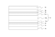
- the light-emitting structure 18 includes: an anode 32 and a cathode disposed oppositely to each other; and a light-emitting material layer 31 disposed between the anode 32 and the cathode.
- the common electrode 16 located below the light-emitting structure serves as the cathode.
- the common electrode 16 is located below the light-emitting structure 18 and serves as the cathode of the light-emitting structure 18 so as to facilitate to decrease the manufacture processes and reduce the production cost.
- the anode 32 together with the common electrode 16 serving as the cathode of the light-emitting structure 18 is configured to supply the light-emitting structure with a driving voltage, which allows the light-emitting structure to generate white light.
- the light-emitting structure 18 further includes: an electron transport layer 33 , a hole transport layer 34 , a first barrier layer 35 and a second barrier layer 36 .
- the electron transport layer 33 is located between the common electrode 16 and the light-emitting material layer 31 , and is configured to introduce electrons into the light-emitting material layer 31 .
- the hole transport layer 34 is located between the light-emitting material layer 31 and the anode 32 , and is configured to introduce holes into the light-emitting material layer 31 .
- the first barrier layer 35 is located between the electron transport layer 33 and the light-emitting material layer 31 , and is configured to block holes to be transported to the common electrode 16 .
- the second barrier layer 36 is located between the hole transport layer 34 and the light-emitting material layer 31 , and is configured to block electrons to be transported to the anode 32 .
- the light-emitting material layer 31 includes: an orange phosphorescent layer 31 a located over the first barrier layer 35 , a blue fluorescence layer 31 b located over the orange phosphorescent layer 31 a , and a green phosphorescent layer 31 c located over the blue fluorescence layer 31 b.
- the light-emitting structure 18 During operation of the light-emitting structure 18 , electrons are injected at the common electrode 16 and introduced into the light-emitting material layer 31 through the electron transport layer 33 , and holes are injected at the anode 32 and introduced into the light-emitting material layer 31 through the hole transport layer 34 ; and then the electrons and the holes are recombined in the light-emitting material layer 31 to form singlet state excitons and triplet state excitons. During transition from excitation state to ground state, the singlet state excitons and the triplet state excitons release their energy in form of photons and thermal energy in which part of the photons are utilized as a backlight source configured to provide light for image display.
- the transition from excitation state to ground state of the singlet state excitons in the blue fluorescence layer 31 b allows emitting blue fluorescence
- the transition from ground state to excitation state of the triplet state excitons in the orange phosphorescent layer 31 a and green phosphorescent layer 31 c allows emitting green fluorescence and orange fluorescence; the blue fluorescence is recombined with the green phosphorescent and orange phosphorescent so as to form the white light.
- the solar cell structure 19 includes: a positive electrode 191 and a negative electrode 192 disposed oppositely to each other; an intrinsic silicon material layer 193 disposed between the positive electrode 191 and the negative electrode 192 ; a P-type silicon material layer 194 disposed between the positive electrode 191 and the intrinsic silicon material layer 193 ; and a N-type silicon material layer 195 disposed between the negative electrode 192 and the intrinsic silicon material layer 193 .
- the P-type silicon material layer 194 and the N-type silicon material layer 195 form a PN junction.
- the solar cell structure 19 is subjected to irradiation, in the PN junction, holes of the N-type silicon material layer 195 transfer to the P-type silicon material layer 194 , while electrons of the P-type silicon material layer 194 transfer to the N-type silicon material layer 195 , so as to form electric current flow from the N-type silicon material layer 195 to the P-type silicon material layer 194 , and then from electrical potential in the PN junction which is connected to an external circuit through the positive electrode 191 and the negative electrode 192 to form a loop.
- the TFT 15 is a bottom gate TFT.
- the gate 151 of the bottom gate TFT is disposed in a same layer as the scanning lines 12 , both of them are located over the substrate 11 ; and the scanning lines 12 are configured to provide the gate 151 with scanning signals.
- the gate 151 is made of a same material as the scanning line 12 .
- the material as used for manufacture typically is nontransparent metal including chromium (Cr), tungsten (W), titanium (Ti), molybdenum (Mo), aluminum (Al) and copper (Cu) or the like, or an alloy thereof.
- the gate insulating layer 152 is located over the layer of the gate 151 and the scanning lines 12 to cover the area over the gate 151 and the scanning lines 12 , and is configured to insulate the gate 151 and the scanning lines 12 from other layers.
- the gate insulating layer is formed of transparent insulating material, such as silicon oxide or silicon nitride, or the like.
- the active layer 153 is located over the gate insulating layer 152 , and is formed of indium gallium zinc oxide (IGZO) or other transition metal oxide.
- the active layer 153 can also be formed of amorphous silicon material or polycrystalline silicon material.
- the active layer 153 is formed of indium gallium zinc oxide (IGZO) or other transition metal oxide, in order to reduce leakage current.
- the source electrode 154 and the drain electrode 155 are disposed in a same layer as the data lines 13 , i.e., all of them are located over the layer of the active layer 153 and are formed of the same material which is typically non-transparent metal material or an alloy thereof.
- the data line 13 is electrically connected to the source electrode 154 .
- the gate 151 is disposed in a same layer as the solar cell structure 19 .
- the gate insulating layer 152 is located over the layer of the gate 151 and the solar cell structure 19 to cover the gate 151 and the solar cell structure 19 .
- Such a design facilitates the solar cell structure receiving irradiation of external light so as to improve the utilization ratio of light and the working efficiency of the solar cell structure.
- the array substrate further includes a barrier layer 21 disposed over the active layer 153 and below the layer of the source electrode 154 and the drain electrode 155 .
- the barrier layer 21 is configured to protect the active layer 153 from being over-etched.
- the barrier layer utilizes transparent insulating material, such as silicon oxide or silicon nitride.
- the barrier layer 21 is provided with a first via hole 211 and a second via hole 212 at locations corresponding to the source electrode 154 and the drain electrode 155 , respectively.
- the source electrode 154 is electrically connected to the active layer 153 through the first via hole 211
- the drain electrode 155 is electrically connected to the active layer 153 through the second via hole 212 .
- the barrier layer 21 and the gate insulating layer 152 are provided with a third via hole 213 at a location corresponding to the power output line 20 , and the positive electrode 191 is electrically connected to the power output line 20 through the third via hole 213 .
- the array substrate further includes a passivation layer 22 .
- the passivation layer 22 is disposed over the layer of the source electrode 154 and the drain electrode 155 to cover the area over the TFT 15 , and is configured to protect the TFT from being eroded.
- the passivation layer 22 is provided with a fifth via hole 215 at a location corresponding to the drain electrode 155 , and the pixel electrode 17 is electrically connected to the drain electrode 155 through the fifth via hole 215 .
- the second embodiment of the present disclosure provides another array substrate.
- the array substrate has a structure substantially same as that of the array substrate as provided by the first embodiment, except that the TFT 15 in the array substrate as provided by the second embodiment is a top gate TFT, and that the solar cell structure 19 is located over the barrier layer 21 and below the gate insulating layer 152 and is disposed in a same layer as the active layer 153 .
- the source electrode 154 and the drain electrode 155 are located over the substrate 11 , and are disposed in a same layer.
- the active layer 153 is located over the layer of the source electrode 154 and the drain electrode 155 .
- the active layer 153 is generally formed by using semiconductor material, such as monocrystalline silicon and polycrystalline silicon. Since the active layer 153 is disposed in a same layer as the solar cell structure 19 , it is possible to form the active layer and the intrinsic silicon material layer of the solar cell structure through a single patterning process, which facilitates reducing the manufacture steps and reducing the production cost.
- the gate insulating layer 152 is located over the active layer 153 to cover the active layer 153 and allow the active layer 153 to be insulated from the gate 151 .
- the gate 151 is located over the gate insulating layer 152 .
- the barrier layer 21 is located over the layer of the source electrode 154 and the drain electrode 155 and below the active layer 153 , and is configured to protect the source electrode and the drain electrode from being over-etched.
- the barrier layer 21 is provided with a first via hole 211 and a second via hole 212 at locations corresponding to the source electrode 154 and the drain electrode 155 , respectively.
- the source electrode 154 is electrically connected to the active layer 153 through the first via hole 211
- the drain electrode 155 is electrically connected to the active layer 153 through the second via hole 212 .
- the barrier layer 21 is provided with a fourth via hole 214 at a location corresponding to the power output line 20 , and the positive electrode 191 is electrically connected to the power output line 20 through the fourth via hole 214 .
- the passivation layer 22 and the barrier layer 21 are provided with a sixth via hole 216 at a location corresponding to the drain electrode 155 , and the pixel electrode 17 is electrically connected to the drain electrode 155 through the sixth via hole 216 .
- the array substrate as provided by the first and second embodiments of the present disclosure includes a light-emitting structure configured to provide a backlight source, a solar cell structure and a power output line.
- the light-emitting structure is disposed between the common electrode and the pixel electrode; the solar cell structure is disposed between the substrate and the common electrode; the power output line is disposed in a same layer as the common electrode, and is electrically connected to the solar cell structure so as to transmit electric energy generated by the solar cell structure to an external circuit, which achieves a combination of the solar energy technology and the OLED display technology.
- a solar cell structure it can generate electric energy to be transmitted to an external circuit which stores the electric energy as received for supplying the array substrate so that the array substrate can operate without external power supply.
- the power output line and the common electrode are disposed in the same layer, and hence can be formed through a single patterning process, which simplifies the manufacture process, reduces the production cost and also shortens the manufacture period.
- the third embodiment of the present disclosure provides a manufacture method of array substrate, including: a step of forming scanning lines, data lines, a common electrode, a pixel electrode and a TFT.
- the step of forming the TFT includes a step of forming a gate, a gate insulating layer, a source electrode, a drain electrode and an active layer, wherein the common electrode, the pixel electrode and the TFT are all formed in a plurality of pixel regions defined by the scanning lines and the data lines.
- the method further includes a step of forming a light-emitting structure, a solar cell structure and a power output line over a substrate.
- the light-emitting structure is disposed between the common electrode and the pixel electrode.
- the solar cell structure is disposed between the array substrate and the common electrode.
- the power output line is disposed in a same layer as the common electrode, and is electrically connected to the solar cell structure so as to transmit electric energy generated by the solar cell structure to an external circuit.
- the first step referring to FIG. 5 , depositing a layer of metal film on the substrate 11 , and then forming a pattern including the gate 151 by a patterning process.
- the material forming the metal film is non-transparent metal including Cr, W, Ti, Ta, Mo, Al and Cu, or the like, or an alloy thereof.
- the solar cell structure 19 In the second step, referring to FIG. 6 , forming a pattern including the solar cell structure 19 over the substrate, wherein the solar cell structure 19 is disposed in a same layer as the gate 151 .
- the third step referring to FIG. 7 , depositing a silicon nitride layer or a silicon oxide layer over the pattern including the solar cell structure 19 to form the gate insulating layer 152 .
- the semiconductor material can be polycrystalline silicon semiconductor material, amorphous silicon semiconductor material or metal oxide semiconductor material.
- the fifth step referring to FIG. 9 , depositing a silicon nitride layer or a silicon oxide layer over the pattern including the active layer 153 to form the barrier layer 21 ; then forming the first via hole 211 and the second via hole 212 at locations in the barrier layer corresponding to the source electrode 154 and the drain electrode 155 , respectively, and forming the third via hole 213 at a location in the barrier layer corresponding to the power output line, wherein the third via hole 213 is penetrating through the barrier layer 21 and the gate insulating layer 152 .
- the sixth step referring to FIG. 10 , depositing a layer of metal film over the barrier layer, and then forming a pattern including the source electrode 154 , the drain electrode 155 , the common electrode 16 and the power output line 20 by a patterning process.
- the source electrode 154 is electrically connected to the active layer 153 through the first via hole 211
- the drain electrode 155 is electrically connected to the active layer 153 through the second via hole 212
- the power output line 20 is electrically connected to the solar cell structure 19 through the third via hole 213 .
- this step includes coating a light-emitting material layer and a transparent conductive material layer over the pattern including the light-emitting structure 18 formed over the pattern including the source electrode 154 , the drain electrode 155 , the common electrode 16 and the power output line 20 , and then forming the light-emitting material layer and the anode of the light-emitting structure through a patterning process, and the common electrode 16 is configured to serve as the cathode of the light-emitting structure 18 .
- the eighth step referring to FIG. 12 , depositing a silicon nitride layer or a silicon oxide layer over the TFT to form a passivation layer configured to protect the TFT from being eroded. Forming the fifth via hole 215 in the passivation layer 22 by a patterning process, which penetrates through the passivation layer and corresponds to the location of the drain electrode 155 .
- the ninth step referring to FIG. 2 , depositing a layer of indium tin oxide (ITO) transparent conductive film over the passivation layer 22 by using a magnetron sputtering method, and forming a pattern including the pixel electrode 17 by a patterning process; wherein the pixel electrode 17 is electrically connected to the drain electrode 155 through the fifth via hole 215 , and the fifth via hole 215 is filled with transparent conductive material configured to form the pixel electrode 17 .
- ITO indium tin oxide
- an array substrate as provided by the first embodiment of the present disclosure having a sectional structure as shown in FIG. 2 is formed by the steps above.
- the manufacture method thereof is similar as that of the array substrate as provided by the first embodiment and includes steps as below.
- the first step referring to FIG. 13 , depositing a layer of metal film on the substrate 11 , and then forming a pattern including the source electrode 154 and the drain electrode 155 by a patterning process.
- the material forming the metal film includes non-transparent metal, such as Cr, W, Ti, Ta, Mo, Al and Cu, or the like, or an alloy thereof.
- the second step referring to FIG. 14 , depositing a silicon nitride layer or a silicon oxide layer over the pattern including the source electrode 154 and the drain electrode 155 to form the barrier layer 21 ; and then forming the first via hole 211 and the second via hole 212 at locations in the barrier layer corresponding to the source electrode 154 and the drain electrode 155 , respectively; the active layer 153 is electrically connected to the source electrode 154 through the first via hole 211 , and is electrically connected to the drain electrode 155 through the second via hole 212 .
- the third step referring to FIG. 15 , depositing transparent conductive material and N-type silicon material in turn over the barrier layer 21 ; and then forming a pattern including the negative electrode 192 and the N-type silicon material layer 192 of the solar cell structure by a patterning process.
- the fourth step referring to FIG. 16 , depositing intrinsic Si material over the pattern including the N-type silicon material layer of the solar cell structure 19 ; and then forming a pattern including the active layer 153 and the intrinsic Si material layer of the solar cell structure 19 by a patterning process, and depositing a layer of metal film over the intrinsic Si material layer to form the positive electrode 191 of the solar cell structure.
- the fifth step referring to FIG. 17 , depositing a silicon nitride layer or a silicon oxide layer over the pattern including the active layer 153 and the intrinsic Si material layer of the solar cell structure 19 to form a gate insulating layer 152 .
- the sixth step referring to FIG. 18 , depositing a layer of metal film over the gate insulating layer 152 , and then forming a pattern including the gate 151 by a patterning process.
- the material forming the metal film includes nontransparent metal, such as Cr, W, Ti, Ta, Mo, Al and Cu, or the like or an alloy thereof.
- the seventh step referring to FIG. 19 , doping the active layer with PH 3 at locations corresponding to the source electrode and the drain electrode by way of iron injection to increase the carrier concentration; and doping the intrinsic Si material in the solar cell structure 19 to form the intrinsic Si material layer 193 and the P-type silicon material layer 194 of the solar cell structure 19 .
- the eighth step referring to FIG. 20 , forming the fourth via hole 214 in the gate insulating layer 152 at a location corresponding to the power output line 20 by a patterning process, wherein the power output line 20 is electrically connected to the solar cell structure 19 through the fourth via hole 214 ; and forming a via hole in the gate insulating layer 152 and the barrier layer 21 at a location corresponding to the drain electrode 155 .
- the ninth step referring to FIG. 21 , depositing a layer of metal film over the pattern including the gate 151 , and forming a pattern including the common electrode 16 and the power output line 20 by a patterning process.
- the common electrode 16 is configured to serve as the cathode of the light-emitting structure 18 .
- the eleventh step referring to FIG. 23 , depositing transparent insulating material including silicon nitride or silicon oxide, or the like, over the pattern including the light-emitting structure 18 to form the passivation layer 22 ; and forming a via hole penetrating through the passivation layer, in the gate insulating layer 152 and in the barrier layer 21 at a location corresponding to the drain electrode 155 , that is, forming the sixth via hole 216 penetrating through the passivation layer 22 , the gate insulating layer 152 and the barrier layer 21 .
- the twelfth step referring to FIG. 4 , depositing a layer of indium tin oxide (ITO) transparent conductive film over the passivation layer 22 by using a magnetron sputtering method, and forming a pattern including the pixel electrode 17 by a patterning process; wherein the pixel electrode 17 is electrically connected to the drain electrode 155 through the sixth via hole 216 , and the sixth via hole 216 is filled with metal conductive material configured to form the common electrode and transparent conductive material configured to form the pixel electrode.
- ITO indium tin oxide
- an array substrate as provided by the second embodiment of the present disclosure having a sectional structure as shown in FIG. 4 is formed by the steps above.
- Embodiments of the present disclosure also provide a display panel including any of the array substrates above.
- the solar cell structure is located on the substrate and is convenient to receive irradiation of external light so as to improve the utilization ratio of light and the working efficiency of the solar cell structure.
- inventions of the present disclosure provide an array substrate, a manufacture method of the same and a display panel.
- the array substrate includes a light-emitting structure, a solar cell structure and a power output line.
- the light-emitting structure is disposed between the common electrode and the pixel electrode.
- the solar cell structure is disposed between the substrate and the common electrode.
- the power output line is disposed in a same layer as the common electrode and is electrically connected to the solar cell structure so as to transmit electric energy generated by the solar cell structure to an external circuit, which achieves a combination of the solar energy technology and the OLED display technology.
- the solar cell structure By means of the solar cell structure, it can generate electric energy to be transferred to an external circuit which stores the electric energy as received for supplying the array substrate so that the array substrate can operate without external power supply. Furthermore, in the array substrate above, the power output line and the common electrode are disposed in A same layer, and hence can be formed through a single patterning process, which simplifies the manufacture process, reduces the production cost and shortens the manufacture period.
Landscapes
- Engineering & Computer Science (AREA)
- Power Engineering (AREA)
- Microelectronics & Electronic Packaging (AREA)
- Physics & Mathematics (AREA)
- Condensed Matter Physics & Semiconductors (AREA)
- General Physics & Mathematics (AREA)
- Computer Hardware Design (AREA)
- Manufacturing & Machinery (AREA)
- Electromagnetism (AREA)
- Ceramic Engineering (AREA)
- Chemical & Material Sciences (AREA)
- Inorganic Chemistry (AREA)
- Life Sciences & Earth Sciences (AREA)
- Sustainable Development (AREA)
- Geometry (AREA)
- Electroluminescent Light Sources (AREA)
- Devices For Indicating Variable Information By Combining Individual Elements (AREA)
Applications Claiming Priority (4)
| Application Number | Priority Date | Filing Date | Title |
|---|---|---|---|
| CN201410130738 | 2014-03-28 | ||
| CN201410130738.X | 2014-03-28 | ||
| CN201410130738.XA CN103928474B (zh) | 2014-03-28 | 2014-03-28 | 一种阵列基板及其制备方法和显示面板 |
| PCT/CN2014/085498 WO2015143836A1 (zh) | 2014-03-28 | 2014-08-29 | 阵列基板及其制备方法和显示面板 |
Publications (2)
| Publication Number | Publication Date |
|---|---|
| US20150380476A1 US20150380476A1 (en) | 2015-12-31 |
| US9620578B2 true US9620578B2 (en) | 2017-04-11 |
Family
ID=51146639
Family Applications (1)
| Application Number | Title | Priority Date | Filing Date |
|---|---|---|---|
| US14/436,517 Active US9620578B2 (en) | 2014-03-28 | 2014-08-29 | Array substrate, manufacture method thereof, and display panel |
Country Status (3)
| Country | Link |
|---|---|
| US (1) | US9620578B2 (zh) |
| CN (1) | CN103928474B (zh) |
| WO (1) | WO2015143836A1 (zh) |
Families Citing this family (13)
| Publication number | Priority date | Publication date | Assignee | Title |
|---|---|---|---|---|
| CN103928474B (zh) * | 2014-03-28 | 2017-03-15 | 京东方科技集团股份有限公司 | 一种阵列基板及其制备方法和显示面板 |
| CN104201187B (zh) * | 2014-08-18 | 2017-07-04 | 京东方科技集团股份有限公司 | 一种oled显示装置 |
| CN104867964B (zh) * | 2015-05-18 | 2019-02-22 | 京东方科技集团股份有限公司 | 阵列基板、其制造方法以及有机发光二极管显示装置 |
| CN105655407A (zh) * | 2016-03-11 | 2016-06-08 | 京东方科技集团股份有限公司 | 多晶硅薄膜晶体管及其制备方法、阵列基板、显示装置 |
| CN106654048B (zh) | 2016-12-27 | 2019-01-25 | 武汉华星光电技术有限公司 | 顶发光型oled显示单元、制作方法及显示面板 |
| CN107272235A (zh) * | 2017-05-12 | 2017-10-20 | 惠科股份有限公司 | 显示设备及其主动式阵列开关基板 |
| CN107425042B (zh) | 2017-07-27 | 2020-05-01 | 京东方科技集团股份有限公司 | 一种oled阵列基板、显示装置 |
| CN107742627A (zh) * | 2017-09-28 | 2018-02-27 | 京东方科技集团股份有限公司 | 显示面板以及显示面板的制备方法 |
| CN109037303B (zh) * | 2018-09-14 | 2020-11-24 | 京东方科技集团股份有限公司 | 有源矩阵有机发光二极管背板及其制造方法、显示面板 |
| CN109755281B (zh) * | 2019-01-14 | 2021-07-06 | 深圳市华星光电半导体显示技术有限公司 | Oled显示面板及其制作方法 |
| CN110895374A (zh) * | 2019-11-26 | 2020-03-20 | 上海天马微电子有限公司 | 显示面板及显示装置 |
| CN110993616B (zh) | 2019-11-28 | 2022-08-09 | 京东方科技集团股份有限公司 | 显示背板及其制备方法和显示装置 |
| CN114913782A (zh) * | 2021-02-09 | 2022-08-16 | 海信视像科技股份有限公司 | 一种显示装置 |
Citations (11)
| Publication number | Priority date | Publication date | Assignee | Title |
|---|---|---|---|---|
| US20020008796A1 (en) * | 2000-06-14 | 2002-01-24 | Jerry Ji-Ho Kung | TFTLCD for recycling electrical power |
| US20050017302A1 (en) * | 2003-07-25 | 2005-01-27 | Randy Hoffman | Transistor including a deposited channel region having a doped portion |
| US20090108757A1 (en) | 2007-10-22 | 2009-04-30 | National Taiwan University | One-piece organic light emitting diode display device with an energy-recycling feature and high contrast |
| CN102117825A (zh) | 2010-01-05 | 2011-07-06 | 三星移动显示器株式会社 | 有机发光显示装置 |
| US20110317121A1 (en) * | 2010-06-28 | 2011-12-29 | Au Optronics Corp. | Flat display device integrated with photovoltaic cell |
| US20120013833A1 (en) * | 2010-07-16 | 2012-01-19 | Wintek Corporation | Liquid crystal display panel |
| US20120326131A1 (en) * | 2011-06-27 | 2012-12-27 | Samsung Mobile Display Co., Ltd. | Organic light emitting diode display |
| US20130187161A1 (en) * | 2012-01-20 | 2013-07-25 | Semiconductor Energy Laboratory Co., Ltd. | Semiconductor device and manufacturing method thereof |
| CN103928474A (zh) | 2014-03-28 | 2014-07-16 | 京东方科技集团股份有限公司 | 一种阵列基板及其制备方法和显示面板 |
| CN203760477U (zh) | 2014-03-28 | 2014-08-06 | 京东方科技集团股份有限公司 | 一种阵列基板和显示面板 |
| US20140295179A1 (en) * | 2013-04-01 | 2014-10-02 | Kabushiki Kaisha Toshiba | Transparent conductive film and electric device |
-
2014
- 2014-03-28 CN CN201410130738.XA patent/CN103928474B/zh active Active
- 2014-08-29 WO PCT/CN2014/085498 patent/WO2015143836A1/zh active Application Filing
- 2014-08-29 US US14/436,517 patent/US9620578B2/en active Active
Patent Citations (11)
| Publication number | Priority date | Publication date | Assignee | Title |
|---|---|---|---|---|
| US20020008796A1 (en) * | 2000-06-14 | 2002-01-24 | Jerry Ji-Ho Kung | TFTLCD for recycling electrical power |
| US20050017302A1 (en) * | 2003-07-25 | 2005-01-27 | Randy Hoffman | Transistor including a deposited channel region having a doped portion |
| US20090108757A1 (en) | 2007-10-22 | 2009-04-30 | National Taiwan University | One-piece organic light emitting diode display device with an energy-recycling feature and high contrast |
| CN102117825A (zh) | 2010-01-05 | 2011-07-06 | 三星移动显示器株式会社 | 有机发光显示装置 |
| US20110317121A1 (en) * | 2010-06-28 | 2011-12-29 | Au Optronics Corp. | Flat display device integrated with photovoltaic cell |
| US20120013833A1 (en) * | 2010-07-16 | 2012-01-19 | Wintek Corporation | Liquid crystal display panel |
| US20120326131A1 (en) * | 2011-06-27 | 2012-12-27 | Samsung Mobile Display Co., Ltd. | Organic light emitting diode display |
| US20130187161A1 (en) * | 2012-01-20 | 2013-07-25 | Semiconductor Energy Laboratory Co., Ltd. | Semiconductor device and manufacturing method thereof |
| US20140295179A1 (en) * | 2013-04-01 | 2014-10-02 | Kabushiki Kaisha Toshiba | Transparent conductive film and electric device |
| CN103928474A (zh) | 2014-03-28 | 2014-07-16 | 京东方科技集团股份有限公司 | 一种阵列基板及其制备方法和显示面板 |
| CN203760477U (zh) | 2014-03-28 | 2014-08-06 | 京东方科技集团股份有限公司 | 一种阵列基板和显示面板 |
Non-Patent Citations (6)
| Title |
|---|
| Dec. 31, 2014-(WO)-International Search Report and Written Opinion PCT/CN2014/085498 English Tran. |
| Dec. 31, 2014—(WO)—International Search Report and Written Opinion PCT/CN2014/085498 English Tran. |
| Feb. 1, 2016-(CN) Office Action-App 201410130738.X-Eng Tran. |
| Feb. 1, 2016—(CN) Office Action—App 201410130738.X—Eng Tran. |
| May 13, 2016-(CN)-Second Office Action Appn 201410130738.X with English Tran. |
| May 13, 2016—(CN)—Second Office Action Appn 201410130738.X with English Tran. |
Also Published As
| Publication number | Publication date |
|---|---|
| US20150380476A1 (en) | 2015-12-31 |
| CN103928474A (zh) | 2014-07-16 |
| CN103928474B (zh) | 2017-03-15 |
| WO2015143836A1 (zh) | 2015-10-01 |
Similar Documents
| Publication | Publication Date | Title |
|---|---|---|
| US9620578B2 (en) | Array substrate, manufacture method thereof, and display panel | |
| US8421090B2 (en) | Organic light emitting diode display and method of manufacturing the same | |
| EP3640986A1 (en) | Oled display panel and manufacturing method therefor | |
| CN102456712B (zh) | 制造柔性显示器的方法 | |
| CN101409304B (zh) | 有机el显示装置 | |
| US20190013339A1 (en) | Organic Light-Emitting Diode (OLED) Array Substrate and Manufacturing Method Thereof and Display Device | |
| US20150144902A1 (en) | Organic Light Emitting Diode Display Device | |
| US10204965B2 (en) | Organic light emitting diode display panels and manufacturing methods thereof, display devices | |
| KR100984362B1 (ko) | 유기 발광 표시판 | |
| US10121830B1 (en) | OLED display panel and manufacturing method thereof | |
| KR20150070753A (ko) | 유기 발광 표시 장치 및 이의 제조 방법 | |
| CN107910347A (zh) | 一种显示器件及oled显示面板 | |
| CN105529350B (zh) | 有机发光二极管显示装置 | |
| CN108987480A (zh) | 双栅薄膜晶体管及其制备方法、显示面板及其制备方法 | |
| GB2530222A (en) | Organic light emitting diode anode connection structure and manufacturing method thereof | |
| CN110164942A (zh) | 一种显示面板及其制备方法、显示装置 | |
| US8686443B2 (en) | Organic light-emitting display device | |
| CN103489892A (zh) | 一种阵列基板及其制作方法和显示装置 | |
| WO2020118988A1 (zh) | 显示面板及其制作方法 | |
| KR20100137272A (ko) | 유기전계발광 표시장치 및 그 제조방법 | |
| KR20110070167A (ko) | 유기전계 발광소자 | |
| TW201334040A (zh) | 用於有機發光顯示器之畫素結構之製造方法 | |
| KR20130008428A (ko) | 유기전계 발광소자 | |
| US9159775B1 (en) | Anode connection structure of organic light-emitting diode and manufacturing method thereof | |
| KR20150021212A (ko) | 유기전계 발광소자의 제조 방법 및 그 방법에 의해 제조된 유기전계 발광소자 |
Legal Events
| Date | Code | Title | Description |
|---|---|---|---|
| AS | Assignment |
Owner name: BEIJING BOE OPTOELECTRONICS TECHNOLOGY CO., LTD., Free format text: ASSIGNMENT OF ASSIGNORS INTEREST;ASSIGNORS:ZHANG, JIAXIANG;GUO, JIAN;CHEN, XU;REEL/FRAME:035480/0943 Effective date: 20150327 Owner name: BOE TECHNOLOGY GROUP CO., LTD., CHINA Free format text: ASSIGNMENT OF ASSIGNORS INTEREST;ASSIGNORS:ZHANG, JIAXIANG;GUO, JIAN;CHEN, XU;REEL/FRAME:035480/0943 Effective date: 20150327 |
|
| STCF | Information on status: patent grant |
Free format text: PATENTED CASE |
|
| MAFP | Maintenance fee payment |
Free format text: PAYMENT OF MAINTENANCE FEE, 4TH YEAR, LARGE ENTITY (ORIGINAL EVENT CODE: M1551); ENTITY STATUS OF PATENT OWNER: LARGE ENTITY Year of fee payment: 4 |