US9620486B2 - Light-emitting diode module - Google Patents
Light-emitting diode module Download PDFInfo
- Publication number
- US9620486B2 US9620486B2 US14/436,486 US201314436486A US9620486B2 US 9620486 B2 US9620486 B2 US 9620486B2 US 201314436486 A US201314436486 A US 201314436486A US 9620486 B2 US9620486 B2 US 9620486B2
- Authority
- US
- United States
- Prior art keywords
- light
- emitting diode
- phosphor
- diode chip
- peak wavelength
- Prior art date
- Legal status (The legal status is an assumption and is not a legal conclusion. Google has not performed a legal analysis and makes no representation as to the accuracy of the status listed.)
- Active
Links
Images


Classifications
-
- H01L25/0753—
-
- H—ELECTRICITY
- H10—SEMICONDUCTOR DEVICES; ELECTRIC SOLID-STATE DEVICES NOT OTHERWISE PROVIDED FOR
- H10W—GENERIC PACKAGES, INTERCONNECTIONS, CONNECTORS OR OTHER CONSTRUCTIONAL DETAILS OF DEVICES COVERED BY CLASS H10
- H10W90/00—Package configurations
-
- H01L33/504—
-
- H01L33/56—
-
- H01L33/58—
-
- H—ELECTRICITY
- H10—SEMICONDUCTOR DEVICES; ELECTRIC SOLID-STATE DEVICES NOT OTHERWISE PROVIDED FOR
- H10H—INORGANIC LIGHT-EMITTING SEMICONDUCTOR DEVICES HAVING POTENTIAL BARRIERS
- H10H20/00—Individual inorganic light-emitting semiconductor devices having potential barriers, e.g. light-emitting diodes [LED]
- H10H20/80—Constructional details
- H10H20/85—Packages
- H10H20/851—Wavelength conversion means
- H10H20/8511—Wavelength conversion means characterised by their material, e.g. binder
- H10H20/8512—Wavelength conversion materials
- H10H20/8513—Wavelength conversion materials having two or more wavelength conversion materials
-
- H—ELECTRICITY
- H10—SEMICONDUCTOR DEVICES; ELECTRIC SOLID-STATE DEVICES NOT OTHERWISE PROVIDED FOR
- H10H—INORGANIC LIGHT-EMITTING SEMICONDUCTOR DEVICES HAVING POTENTIAL BARRIERS
- H10H20/00—Individual inorganic light-emitting semiconductor devices having potential barriers, e.g. light-emitting diodes [LED]
- H10H20/80—Constructional details
- H10H20/85—Packages
- H10H20/852—Encapsulations
- H10H20/854—Encapsulations characterised by their material, e.g. epoxy or silicone resins
-
- H—ELECTRICITY
- H10—SEMICONDUCTOR DEVICES; ELECTRIC SOLID-STATE DEVICES NOT OTHERWISE PROVIDED FOR
- H10H—INORGANIC LIGHT-EMITTING SEMICONDUCTOR DEVICES HAVING POTENTIAL BARRIERS
- H10H20/00—Individual inorganic light-emitting semiconductor devices having potential barriers, e.g. light-emitting diodes [LED]
- H10H20/80—Constructional details
- H10H20/85—Packages
- H10H20/855—Optical field-shaping means, e.g. lenses
-
- H01L2924/00—
-
- H01L2924/0002—
-
- H01L2933/0083—
-
- H—ELECTRICITY
- H10—SEMICONDUCTOR DEVICES; ELECTRIC SOLID-STATE DEVICES NOT OTHERWISE PROVIDED FOR
- H10H—INORGANIC LIGHT-EMITTING SEMICONDUCTOR DEVICES HAVING POTENTIAL BARRIERS
- H10H20/00—Individual inorganic light-emitting semiconductor devices having potential barriers, e.g. light-emitting diodes [LED]
- H10H20/80—Constructional details
- H10H20/872—Periodic patterns for optical field-shaping, e.g. photonic bandgap structures
Definitions
- a light-emitting diode module is specified.
- Various embodiments provide a light-emitting diode module which, after switch-on, exhibits a small change in a color locus of an emitted radiation.
- the module is a light-emitting diode module. That means that a main proportion or an entire radiation generated in the module is generated by optoelectronic semiconductor chips such as light-emitting diodes.
- the light-emitting diodes are preferably based on an inorganic semiconductor material. It is possible for the light-emitting diode module to include further semiconductor chips, not provided for generating radiation. Such semiconductor chips can serve for protection against damage from electrostatic discharges or else for driving individual radiation-generating components of the light-emitting diode module.
- the light-emitting diode module includes at least one first light-emitting diode chip.
- the first light-emitting diode chip is designed for generating radiation in the blue spectral range.
- the radiation generated by the first light-emitting diode chip during operation has a first peak wavelength.
- the peak wavelength is that wavelength at which a maximum intensity is generated.
- the light-emitting diode module includes one or a plurality of second light-emitting diode chips.
- the at least one second light-emitting diode chip is designed for generating radiation in the blue spectral range having a second peak wavelength.
- the first and second peak wavelengths can be identical or different from one another.
- the light-emitting diode module includes one or a plurality of third light-emitting diode chips.
- the at least one third light-emitting diode chip is designed to generate a radiation in the red spectral range during operation. Radiation having a third peak wavelength is therefore emitted by the third light-emitting diode chip.
- the light-emitting diode chips each include a semiconductor layer sequence having at least one active layer.
- the light-emitting diode chips are in each case separate, non-monolithically integrated semiconductor bodies.
- the active layers of the respective semiconductor bodies can preferably be energerized independently of one another.
- said light-emitting diode chips it is also possible for said light-emitting diode chips to include a common semiconductor body, wherein an active zone does not, however, extend continuously over the first and second light-emitting diode chips.
- the semiconductor layer sequence is preferably based on a III-V compound semiconductor material.
- the semiconductor material is for example a nitride compound semiconductor material such as Al n In 1-n-m Ga m N or a phosphide compound semiconductor material such as Al n In 1-n-m Ga m P or else an arsenide compound semiconductor material such as Al n In 1-n-m Ga m As, wherein in each case 0 ⁇ n ⁇ 1, 0 ⁇ m ⁇ 1 and n+m ⁇ 1.
- the semiconductor layer sequence may include dopants and additional constituents.
- the first and second light-emitting diode chips are based on AlInGaN and the third light-emitting diode chip is based on AlInGaP.
- the light-emitting diode module includes a first phosphor or a first phosphor mixture.
- the first phosphor is disposed downstream of the first light-emitting diode chip. That means that a predominant proportion or the entire radiation emitted by the first light-emitting diode chip passes to the first phosphor.
- the first phosphor can be fitted indirectly or directly on the first light-emitting diode chip.
- the light-emitting diode module includes a second phosphor or a second phosphor mixture.
- the second phosphor is fitted directly or indirectly to the second light-emitting diode chip and is disposed downstream of the second light-emitting diode chip along a main emission direction.
- the light-emitting diode module is designed for emitting white light.
- White light means, for example, that a color locus of a total radiation emitted by the light-emitting diode module in the CIE standard chromaticity diagram is at a distance from the black body curve, also designated as the Planckian locus, of at most 0.03 unit or of at most 0.015 unit.
- the correlated color temperature, CCT for short is preferably between 2400 K and 7000 K inclusive.
- the first light-emitting diode chip together with the first phosphor emits a first mixed radiation.
- the second light-emitting diode chip together with the second phosphor emits a second mixed radiation.
- the color loci also referred to as chromaticity coordinates, in the CIE standard chromaticity diagram are preferably above the Planckian locus.
- the mixed radiations are white-green light, designated as mint.
- a c x coordinate of the color locus of the mixed radiations is preferably at least 0.15 and a c y coordinate is preferably at least 0.25.
- the first phosphor has a first absorption maximum.
- the first absorption maximum is at a wavelength that is greater than the first peak wavelength of the radiation generated by the first light-emitting diode chip. It is possible for an absorption of the first phosphor at the first peak wavelength to increase toward greater wavelengths.
- the second phosphor has a second absorption maximum.
- the second absorption maximum is preferably different from the first absorption maximum.
- the second absorption maximum is at a wavelength that is less than the second peak wavelength.
- the absorption of the second phosphor can decrease, in the direction toward greater wavelengths.
- the first phosphor and the second phosphor, with respect to the absorption profile can have gradients having different signs.
- the absorption maximum is not precluded from being at significantly shorter wavelengths than the second peak wavelength.
- the second absorption maximum can also be in the ultraviolet spectral range.
- the light-emitting diode module includes at least one first light-emitting diode chip designed for generating radiation in the blue spectral range having a first peak wavelength, and at least one second light-emitting diode chip designed for generating radiation in the blue spectral range having a second peak wavelength. At least one third light-emitting diode chip of the light-emitting diode module is designed for generating radiation in the red spectral range having a third peak wavelength.
- a first phosphor is disposed downstream of the first light-emitting diode chip and a second phosphor is disposed downstream of the second light-emitting diode chip.
- the light-emitting diode module is designed for emitting white light.
- the first light-emitting diode chip together with the first phosphor emits a first mixed radiation and the second light-emitting diode chip together with the second phosphor generates a second mixed radiation.
- the first phosphor has a first absorption maximum at a wavelength that is greater than the first peak wavelength.
- a second absorption maximum of the second phosphor is at a wavelength that is less than the second peak wavelength.
- LEDs for short which are intended to have a high color rendering index, RA for short
- InGaN light-emitting diode chips that emit in the blue spectral range
- InGaAlP light-emitting diode chips that emit in the red spectral range.
- Such a shift in the cumulative color locus takes place for example on a time scale of at least five minutes or of at least ten minutes and/or of at most 60 minutes or of at most 30 minutes or of at most 20 minutes.
- Such a shift after switch-on is undesirable particularly in general lighting or in the lighting of display devices having in some instances only a short average switched-on duration.
- such a color locus shift in some instances is likewise not tolerable.
- the light-emitting diode module includes two different phosphors having different absorption characteristics in the blue spectral range. If the temperature of the first light-emitting diode chip rises and the peak wavelength thereof shifts toward greater wavelengths, then the relative proportion of radiation of the first light-emitting diode chip that is absorbed and converted in the first phosphor decreases. Furthermore, an increasing proportion of radiation from the second light-emitting diode chip is absorbed in the second phosphor. This has the effect, in particular, that a color locus of the total radiation emitted by the light-emitting diode module in the event of a temperature change does not shift or shifts to a lesser extent.
- the first phosphor has a dominant emission wavelength of at least 570 nm or of at least 572 nm or of at least 574 nm.
- a dominant emission wavelength of the second phosphor is at most 570 nm or at most 566 nm or at most 562 nm.
- the dominant wavelength is, in particular, that wavelength which results as the point of intersection of the spectrum locus of the CIE standard chromaticity diagram with a straight line, wherein said straight line, proceeding from the white point in the CIE standard chromaticity diagram, runs through the actual color locus of the radiation.
- the dominant wavelength differs from the peak wavelength.
- the first absorption maximum of the first phosphor is at least 450 nm or at least 452 nm. Alternatively or additionally, the first absorption maximum is at most 470 nm or at most 465 nm or at most 460 nm.
- the second absorption maximum of the second phosphor is at least 425 nm or at least 430 nm. Alternatively or additionally, the second absorption maximum is at most 442 nm or at most 439 nm.
- the first peak wavelength and/or the second peak wavelength are/is at least 440 nm or at least 442 nm. Alternatively or additionally, said value is at most 465 nm or at most 462 nm.
- the third peak wavelength is at least 610 nm or at least 615 nm. Alternatively or additionally, the third peak wavelength is at most 670 nm or at most 660 nm.
- a color locus of the first mixed radiation in the CIE standard chromaticity diagram lies on or within a quadrilateral having the vertexes having the following coordinates: (0.32; 0.36), (0.48; 0.48), (0.40; 0.56) and (0.32; 0.40) or (0.32; 0.40), (0.42; 0.44), (0.46; 0.50) and (0.38; 0.52).
- the vertexes are specified in coordinate form (c x ; c y ).
- This target color locus range of the first mixed radiation can be set, firstly, by a choice of the first peak wavelength and by the amount of the first phosphor disposed downstream of the first light-emitting diode chip.
- the indication of the color locus range thus corresponds to an indication of the proportion of the radiation to be converted by the first phosphor and the first peak wavelength.
- a color locus of the second mixed radiation lies in or on a quadrilateral having the following vertexes: (0.22; 0.20), (0.30; 0.40), (0.24; 0.46) and (0.18; 0.22) or (0.20; 0.28), (0.24; 0.26), (0.28; 0.34) and (0.24; 0.38).
- a mixed color locus from the first mixed radiation and from the second mixed radiation lies in or on a quadrilateral having the following vertexes: (0.34; 0.38), (0.42; 0.44), (0.38; 0.46) and (0.32; 0.42).
- a ratio of the intensities of the first mixed radiation and of the second mixed radiation is predefined by the mixed color locus.
- the color locus range for the mixed color locus therefore indicates in what ratio the first mixed radiation is to be mixed with the second mixed radiation.
- a color locus of the first mixed radiation together with the radiation emitted by the third light-emitting diode chip lies on the black body curve in the CIE standard chromaticity diagram, with a tolerance of at most 0.03 unit or of at most 0.015 unit.
- this color locus lies with the stated tolerance on the black body curve at a correlated color temperature of 3000 K.
- a higher radiation proportion of the radiation generated by the first light-emitting diode chip is absorbed by the first phosphor, relative to the radiation proportion of the second light-emitting diode chip that is absorbed by the second phosphor.
- the first mixed radiation then has a smaller blue proportion than the second mixed radiation.
- the first peak wavelength is less than the second peak wavelength.
- a wavelength difference between the peak wavelengths is then preferably at least 6 nm or at least 8 nm. Alternatively or additionally, said wavelength difference is at most 18 nm or at most 15 nm.
- the first peak wavelength is equal to the second peak wavelength, in particular with a tolerance of at most 3 nm or of at most 1 nm.
- the first light-emitting diode chip and the second light-emitting diode chip can then be structurally identical, within the scope of the production tolerances.
- the second light-emitting diode chip is designed to be operated with at least 15% or with at least 25% and/or with at most 60% or with at most 50% of the current density and/or of the luminous flux of the first light-emitting diode chip.
- the stated values with regard to the current density apply, in particular, to structurally identical first and second light-emitting diode chips. If the first light-emitting diode chip has a different active, light-generating area than the second light-emitting diode chip, the values for the current density should be correspondingly converted or the luminous flux should be used as the characteristic variable. By way of example, the light-emitting diode chips are then operated approximately with the same current density if the second light-emitting diode chip has a smaller active area than the first light-emitting diode chip.
- the light-emitting diode chips can be energerized variably.
- the relative currents of the first, second and third light-emitting diode chips can be set variably with respect to one another.
- a color temperature of the white light emitted by the light-emitting diode module can be tuned.
- a tuning range is preferably at least 1600 K or at least 2500 K or at least 3000 K.
- the tuning range is between 2700 K and 6000 K inclusive.
- a current intensity can be regulated or pulse width modulation is employed.
- that proportion of the luminous flux emitted overall by the light-emitting diode module which is generated by the third light-emitting diode chip is at least 3% or at least 5% or at least 10%. Alternatively or additionally, said proportion is at most 30% or at most 25% or at most 20%. In other words, the third light-emitting diode chip then contributes only comparatively little to a brightness of the light-emitting diode module.
- the first phosphor is a Y 3 Al 5 O 12 :Ce or a Y 3 (Al,Ga) 5 O 12 :Ce.
- the Ce content is preferably at least 2% or at least 3% and/or at most 6% or at most 5%, in particular approximately 4%.
- the second phosphor is a Y 3 (Al,Ga) 5 O 12 :Ce, an (Lu,Y) 3 (Al,Ga) 5 O 12 :Ce, an Lu 3 (Al,Ga) 5 O 12 :Ce, an orthosilicate or a nitrido-orthosilicate.
- the Ce proportion is preferably at least 1.5% or at least 2% and/or at most 5% or at most 4%, in particular approximately 3%.
- the Ga proportion is preferably at least 20% and/or at most 30%, in particular approximately 25%.
- a first scattering body is disposed downstream of the first and/or the second light-emitting diode chip.
- the first scattering body has a smaller scattering capability at room temperature, in particular at approximately 300 K, than at a steady-state operating temperature of the light-emitting diode module.
- the steady-state operating temperature is, in particular, at least 350 K or 360 K and/or at most 400 K or 425 K, for instance approximately 375 K.
- the first scattering body includes a matrix material and scattering particles embedded into the matrix material.
- a refractive index difference between said matrix material and said scattering particles is smaller at room temperature than at the steady-state operating temperature.
- the refractive index difference at room temperature is at least 0.025 or 0.03 and/or at most 0.05, and at the steady-state operating temperature is at most 0.02 or at most 0.01.
- a scattering effect increases as the temperature increases toward the steady-state operating temperature. This has the effect that in the phosphor, as the temperature increases, the radiation having the first peak wavelength covers a larger average path length and a conversion efficiency of this radiation thus rises. Less radiation having the first peak wavelength or the second peak wavelength then passes from the light-emitting diode module if the temperature increases.
- the proportion of blue light in the first and second mixed radiations can be reduced as the temperature rises toward the steady-state operating temperature and the effect of the shifting of the wavelength of the radiation emitted by the first and second light-emitting diode chips can be reduced or compensated for.
- the first scattering body is integrated in a body containing the first or the second phosphor.
- a single lamina is then involved, for example, which is disposed downstream of the first and/or the second light-emitting diode-chip and which includes both the first scattering body and the first phosphor or the second phosphor.
- a second scattering body is disposed downstream of the third light-emitting diode chip.
- the second scattering body has a greater scattering capability at a temperature of 300 K than at the steady-state operating temperature of approximately 375 K.
- the second scattering body likewise includes a matrix material and scattering particles embedded into the matrix material, wherein a refractive index difference between said matrix material and said scattering particles is greater at room temperature than at the steady-state operating temperature.
- the refractive index difference at room temperature is at most 0.05 or at most 0.04 and/or at least 0.01 or at least 0.03.
- the refractive index difference is, in particular, at most 0.01 or at most 0.03, preferably approximately zero.
- the scattering effect decreases as the temperature increases.
- a transmissivity of the second scattering body to red light then likewise increases as the temperature increases toward the steady-state operating temperature.
- a decrease in the efficiency of the third light-emitting diode chip, toward the steady-state operating temperature, can be at least partly compensated for as a result of this.
- the first and/or the second scattering body include(s) as matrix material a silicone, a silicone-epoxy hybrid material or an epoxy.
- the matrix material of the first scattering body is, for example, a low refractive index silicone, for instance having a refractive index of 1.41+/ ⁇ 0.02 at 300 K.
- the matrix material of the second scattering body can be a high refractive index silicone having a refractive index of approximately 1.51+/ ⁇ 0.02 at room temperature.
- the scattering particles of the first and/or of the second scattering body are formed from one or a plurality of the materials mentioned below or consist of: a glass, quartz, silicon dioxide, a metal fluoride such as barium fluoride, calcium fluoride or magnesium fluoride.
- a glass, quartz, silicon dioxide, a metal fluoride such as barium fluoride, calcium fluoride or magnesium fluoride.
- the refractive indexes of these materials for the scattering particles change only little in dependence on the temperature, in comparison with the refractive index of the matrix material.
- An average diameter of the scattering particles is for example at least 50 nm or at least 150 nm or at least 250 nm or at least 400 nm. Alternatively or additionally, the average diameter of the scattering particles is at most 20 ⁇ m or at most 12 ⁇ m or at most 8 ⁇ m or at most 2 ⁇ m. A proportion by weight of the scattering particles, relative to the matrix material, is preferably at least 1% and/or at most 50% or at most 20% or at most 12% or at most 5%.
- the phosphors include phosphor particles that are embedded into a matrix material.
- the matrix material for the phosphor particles can be the same material as for the scattering particles.
- An average diameter of the phosphor particles is for example at least 2 ⁇ m or at least 3 ⁇ m or at least 5 ⁇ m. Alternatively or additionally, the average diameter is at most 20 ⁇ m or at most 15 ⁇ m or at most 40 ⁇ m.
- the phosphor particles have a larger diameter than the scattering particles.
- a covering layer is disposed jointly downstream of the light-emitting diode chips.
- the covering layer includes at least one scattering medium. An intermixing of the radiation proportions emitted by the individual light-emitting diode chips, jointly with the phosphors, can be improved by the covering layer.
- the covering layer can be shaped as a covering plate disposed downstream of the light-emitting diode chips.
- the covering layer can likewise be a potting into which the light-emitting diode chips are embedded.
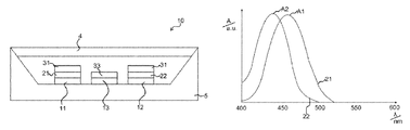
- FIG. 1 shows a schematic sectional illustration of one embodiment of a light-emitting diode module described here
- FIGS. 2A to 2C and 3-7 show schematic illustrations concerning optical properties of embodiments of light-emitting diode modules described here.
- FIG. 1 illustrates one embodiment of a light-emitting diode module 10 .
- a first light-emitting diode chip 11 , a second light-emitting diode chip 12 and a third light-emitting diode chip 13 are fitted to a carrier 5 .
- the light-emitting diode chips 11 , 12 are designed for generating blue light
- the third light-emitting diode chip 13 is designed for generating red light.
- a first phosphor 21 is assigned to the first light-emitting diode chip 11 and a second phosphor 22 is assigned to the second light-emitting diode chip 12 .
- the phosphors 21 , 22 are integrated in a laminar body, for example, and can be applied directly to the light-emitting diode chips 11 , 12 , for example by being printed or adhesively bonded by an adhesive.
- a first scattering body 31 is disposed downstream of the two light-emitting diode chips 11 , 12 .
- the first scattering body 31 can be integrated in the bodies for the phosphors 21 , 22 .
- a second scattering body 33 is preferably disposed downstream of the third light-emitting diode chip 13 .
- the first scattering bodies 31 have a more highly scattering effect as the temperature increases, toward a steady-state operating temperature.
- the second scattering body 33 has a decreasing or vanishing scattering effect toward the steady-state operating temperature, proceeding from room temperature.
- a covering layer 4 is furthermore optionally disposed downstream of the light-emitting diode chips 11 , 12 , 13 , said covering layer including a scattering medium for homogenizing the radiation emitted by the semiconductor chips 11 , 12 , 13 .
- the covering layer 4 can also be realized as a potting, rather than as a plate.
- each case only one first light-emitting diode chip 11 , one second light-emitting diode chip 12 and one third light-emitting diode chip 13 are present. In a departure from this, in each case a plurality of the light-emitting diode chips 11 , 12 , 13 can be used in the light-emitting diode module 10 . In the illustration in accordance with FIG. 1 , the third light-emitting diode chip 13 is situated between the two light-emitting diode chips 11 , 12 . A different arrangement of the light-emitting diode chips 11 , 12 , 13 can likewise be realized.
- the table in FIG. 3 indicates in each case a ratio of the currents I 2 through the second light-emitting diode chip 12 and I 1 through the first light-emitting diode chip 11 , the peak wavelengths L 1 , L 2 of the light-emitting diode chips 11 , 12 , a color locus shift ⁇ C, a color rendering index RA and an efficiency ⁇ .
- the color locus shift ⁇ C is indicated in MacAdam steps, relative to a temperature difference from 90° C. to 25° C. If other phosphors or light-emitting diode chips are used, then the parameters dependent thereon should be adapted accordingly in each case.
- FIG. 2A illustrates emission spectra of the light-emitting diode chips 11 , 12 , 13 schematically and in a normalized manner.
- the first and second light-emitting diode chips 11 , 12 have an identical peak wavelength L 1 , L 2 , which is approximately 455 nm.
- Such light-emitting diode chips 11 , 12 are incorporated in the embodiments A, B and E.
- the third light-emitting diode chip 13 has in each case a third peak wavelength L 3 , which is approximately 625 nm.
- a corresponding third light-emitting diode chip 13 is used in the embodiments A to E.
- the phosphors in accordance with FIGS. 2B and 2C are likewise used for all the embodiments A to E.
- the first phosphor 21 has an absorption maximum A 1 at approximately 460 nm.
- the first phosphor 21 is a YAG: Ce having a Ce content of 4%.
- the second phosphor 22 has an absorption maximum A 2 at approximately 435 nm and is formed by an LuAGaG:Ce including 25% Ga and 3% Ce.
- the second phosphor 22 emits at a shorter emission wavelength than the first phosphor 21 , see FIG. 2C .
- the light-emitting diode chips 11 , 12 are respectively assigned one of the phosphors 21 , 22 .
- a color locus of the corresponding mixed radiations M 1 , M 2 formed by a mixture of the radiation emitted by the light-emitting diode chip 11 , 12 and the radiation converted by the associated phosphor 21 , 22 , can be seen in FIG. 4 .
- a mixed color locus from the mixed radiations M 1 , M 2 is likewise depicted in FIG. 4 .
- the phosphor concentrations of the phosphors 21 , 22 were set in each case separately from one another such that with each of the two light-emitting diode chips 11 , 12 , together with the associated phosphor 21 , 22 , and jointly with the third light-emitting diode chip 13 , a color locus at a color locus temperature of 3000 K can approximately impinge on the black body curve, see FIG. 4 .
- the second light-emitting diode chip 12 is operated only with approximately one fifth of the current of the first light-emitting diode chip 11 , the two light-emitting diode chips 11 , 12 being structurally identical, see the table in FIG. 3 .
- a shift ⁇ C in the mixed color locus from the mixed radiations M 1 , M 2 from the light-emitting diode chips 11 , 12 and the phosphors 21 , 22 is illustrated in FIG. 5 , relative to temperatures of 25° C. and 90° C.
- a color locus shift is reduced in the case of the embodiment A, see the circles.
- the first phosphor 21 on the first light-emitting diode chip 11 is more highly concentrated than the second phosphor 22 on the second light-emitting diode chip 12 .
- the mixed radiation M 2 is therefore shifted further into the blue than in the embodiment A, see FIG. 4 .
- a mixed color locus from the mixed radiations M 1 , M 2 corresponds to that of the embodiment A, likewise see FIG. 4 .
- a color locus shift can be reduced further toward the operating temperature, in comparison with the embodiment A, also see the squares in FIG. 5 .
- One advantage in the case of the embodiment B is that deviations of the phosphor concentrations of the phosphors 21 , 22 from a desired value in production on account of manufacturing tolerances can be adjusted by the variation of a ratio I 2 /I 1 of currents through the light-emitting diode chips 11 , 12 .
- the light-emitting diode chips 11 , 12 have different peak wavelengths L 1 , L 2 .
- a difference between the peak wavelengths L 1 , L 2 is approximately 15 nm.
- a higher color rendering index RA can be obtained as a result.
- the first peak wavelength L 1 is less than the second peak wavelength L 2 .
- the radiation emitted by the first light-emitting diode chip 11 is in a wavelength range with an absorption change of the first phosphor 21 that is greater as the temperature increases.
- the second light-emitting diode chip 12 was chosen to emit at longer wavelengths, such that the absorption of the second phosphor 22 decreases to a greater extent upon a shift to higher wavelengths.
- the values for the current in the table in FIG. 3 are only rough guideline values and are therefore indicted between parentheses.
- the proportion of the luminous flux of the third light-emitting diode chip 13 in the total radiation of the light-emitting diode module 10 was reduced further.
- the mixed radiations M 1 , M 2 moved nearer to the black body curve in the CIE standard chromaticity diagram. A distance from the black body curve is in each case preferably at most 0.7 or at most 0.6 or at most 0.5 unit.
- the color loci of the mixed radiations M 1 , M 2 are moved nearer to the color locus of the white light emitted overall by the light-emitting diode module 10 .
- a reduction of the color rendering index RA as a result can be compensated for by the different peak wavelengths L 1 , L 2 .
- a particularly small color locus shift ⁇ C and a high efficiency ⁇ can be achieved, see FIG. 3 .
- the embodiment E is based on the embodiment B.
- the light-emitting diode chips 11 , 12 , 13 can be operated electrically independently of one another.
- a correlated color temperature of the overall white radiation can be set over a range of 2700 K to 6000 K, see FIG. 6 .
- the average color locus shift ⁇ C at a specific correlated color temperature is comparatively small in this case, likewise see FIG. 6 .
- the color rendering index RA is in each case above 90 and the efficiency ⁇ is in each case approximately 100 lm/W.
- the ratios of the currents I 1 , I 2 , I 3 through the light-emitting diode chips 11 , 12 , 13 are illustrated in FIG. 7 . Since in particular the efficiency of the third light-emitting diode chip 13 based on InAlGaP can vary, the values illustrated should be understood only as rough guideline values.
- the scattering bodies 31 , 33 shown in association with FIG. 1 and/or the covering layer 4 can be present.
- the first phosphor 21 is preferably a garnet.
- the second phosphor 22 is in each case a garnet, but can likewise be an Eu-doped orthosilicate or nitrido-orthosilicate.
Landscapes
- Led Device Packages (AREA)
Applications Claiming Priority (4)
| Application Number | Priority Date | Filing Date | Title |
|---|---|---|---|
| DE102012219460 | 2012-10-24 | ||
| DE102012219460.6A DE102012219460A1 (de) | 2012-10-24 | 2012-10-24 | Leuchtdiodenmodul |
| DE102012219460.6 | 2012-10-24 | ||
| PCT/EP2013/071670 WO2014063976A1 (de) | 2012-10-24 | 2013-10-16 | Leuchtdiodenmodul |
Publications (2)
| Publication Number | Publication Date |
|---|---|
| US20160126221A1 US20160126221A1 (en) | 2016-05-05 |
| US9620486B2 true US9620486B2 (en) | 2017-04-11 |
Family
ID=49488560
Family Applications (1)
| Application Number | Title | Priority Date | Filing Date |
|---|---|---|---|
| US14/436,486 Active US9620486B2 (en) | 2012-10-24 | 2013-10-16 | Light-emitting diode module |
Country Status (5)
| Country | Link |
|---|---|
| US (1) | US9620486B2 (de) |
| EP (1) | EP2912688B1 (de) |
| CN (1) | CN104756251B (de) |
| DE (1) | DE102012219460A1 (de) |
| WO (1) | WO2014063976A1 (de) |
Cited By (2)
| Publication number | Priority date | Publication date | Assignee | Title |
|---|---|---|---|---|
| WO2020028337A1 (en) * | 2018-07-30 | 2020-02-06 | Lumileds Llc | Light-emitting device with light scatter tuning to control color shift |
| US10756242B2 (en) | 2018-07-30 | 2020-08-25 | Lumileds Llc | Light-emitting device with light scatter tuning to control color shift |
Families Citing this family (13)
| Publication number | Priority date | Publication date | Assignee | Title |
|---|---|---|---|---|
| WO2016139954A1 (en) * | 2015-03-05 | 2016-09-09 | Nichia Corporation | Light emitting device |
| JP6632834B2 (ja) * | 2015-08-24 | 2020-01-22 | スタンレー電気株式会社 | 発光装置 |
| JP6384468B2 (ja) * | 2015-12-22 | 2018-09-05 | 日亜化学工業株式会社 | 発光装置 |
| DE102016102596A1 (de) * | 2016-02-15 | 2017-08-17 | Osram Opto Semiconductors Gmbh | Verfahren zum Betreiben einer Halbleiterlichtquelle und Halbleiterlichtquelle |
| DE102016114921A1 (de) | 2016-08-11 | 2018-02-15 | Osram Opto Semiconductors Gmbh | Silikonzusammensetzung |
| US9935144B1 (en) * | 2016-11-28 | 2018-04-03 | Omnivision Technologies, Inc. | System-in-package image sensor |
| US20190296188A1 (en) * | 2017-01-10 | 2019-09-26 | PlayNitride Display Co., Ltd. | Micro light-emitting diode chip |
| JP6917179B2 (ja) * | 2017-04-18 | 2021-08-11 | スタンレー電気株式会社 | 白色発光装置 |
| DE102018124591B4 (de) | 2018-10-05 | 2026-03-19 | OSRAM Opto Semiconductors Gesellschaft mit beschränkter Haftung | Optoelektronisches halbleiterbauelement mit definierter farbpunktverschiebung und verfahren zur herstellung eines optoelektronischen halbleiterbauelements mit definierter farbpunktverschiebung |
| US11870016B2 (en) | 2019-12-02 | 2024-01-09 | Seoul Semiconductor Co., Ltd. | Light emitting device and lighting apparatus including the same |
| CN111223979B (zh) * | 2019-12-04 | 2021-04-16 | 旭宇光电(深圳)股份有限公司 | 健康照明用的发光装置和灯具 |
| US11211414B2 (en) | 2019-12-23 | 2021-12-28 | Omnivision Technologies, Inc. | Image sensor package |
| US11411146B2 (en) * | 2020-10-08 | 2022-08-09 | Lumileds Llc | Protection layer for a light emitting diode |
Citations (8)
| Publication number | Priority date | Publication date | Assignee | Title |
|---|---|---|---|---|
| WO2005062391A1 (en) | 2003-12-23 | 2005-07-07 | Luxpia Co., Ltd. | Yellow emitting phosphor and white semiconductor light emitting device incorporating the same |
| US20070018558A1 (en) * | 2005-07-21 | 2007-01-25 | Chua Janet Bee Y | Device and method for emitting output light using multiple light sources with photoluminescent material |
| US20070223219A1 (en) | 2005-01-10 | 2007-09-27 | Cree, Inc. | Multi-chip light emitting device lamps for providing high-cri warm white light and light fixtures including the same |
| DE102008025864A1 (de) | 2008-05-29 | 2009-12-03 | Lumitech Produktion Und Entwicklung Gmbh | LED Modul für die Allgemeinbeleuchtung |
| DE102010034915A1 (de) | 2010-08-20 | 2012-02-23 | Osram Opto Semiconductors Gmbh | Optoelektronisches Halbleiterbauteil und Streukörper |
| DE102011013504A1 (de) | 2011-03-10 | 2012-09-13 | Osram Opto Semiconductors Gmbh | Licht emittierende Vorrichtung |
| US20120267997A1 (en) * | 2005-03-18 | 2012-10-25 | Mitsubishi Chemical Corporation | Light-emitting device, white light-emitting device, illuminator, and image display |
| DE102011085645A1 (de) | 2011-11-03 | 2013-05-08 | Osram Gmbh | Leuchtdiodenmodul und Verfahren zum Betreiben eines Leuchtdiodenmoduls |
-
2012
- 2012-10-24 DE DE102012219460.6A patent/DE102012219460A1/de not_active Withdrawn
-
2013
- 2013-10-16 WO PCT/EP2013/071670 patent/WO2014063976A1/de not_active Ceased
- 2013-10-16 CN CN201380055577.6A patent/CN104756251B/zh active Active
- 2013-10-16 EP EP13783277.0A patent/EP2912688B1/de active Active
- 2013-10-16 US US14/436,486 patent/US9620486B2/en active Active
Patent Citations (11)
| Publication number | Priority date | Publication date | Assignee | Title |
|---|---|---|---|---|
| WO2005062391A1 (en) | 2003-12-23 | 2005-07-07 | Luxpia Co., Ltd. | Yellow emitting phosphor and white semiconductor light emitting device incorporating the same |
| US20070223219A1 (en) | 2005-01-10 | 2007-09-27 | Cree, Inc. | Multi-chip light emitting device lamps for providing high-cri warm white light and light fixtures including the same |
| US20120267997A1 (en) * | 2005-03-18 | 2012-10-25 | Mitsubishi Chemical Corporation | Light-emitting device, white light-emitting device, illuminator, and image display |
| US20070018558A1 (en) * | 2005-07-21 | 2007-01-25 | Chua Janet Bee Y | Device and method for emitting output light using multiple light sources with photoluminescent material |
| DE102008025864A1 (de) | 2008-05-29 | 2009-12-03 | Lumitech Produktion Und Entwicklung Gmbh | LED Modul für die Allgemeinbeleuchtung |
| DE102010034915A1 (de) | 2010-08-20 | 2012-02-23 | Osram Opto Semiconductors Gmbh | Optoelektronisches Halbleiterbauteil und Streukörper |
| US20140175478A1 (en) | 2010-08-20 | 2014-06-26 | Osram Opto Semiconductors Gmbh | Optoelectronic semiconductor component and scattering body |
| DE102011013504A1 (de) | 2011-03-10 | 2012-09-13 | Osram Opto Semiconductors Gmbh | Licht emittierende Vorrichtung |
| US20130299857A1 (en) | 2011-03-10 | 2013-11-14 | Osram Opto Semiconductors Gmbh | Light-Emitting Device |
| DE102011085645A1 (de) | 2011-11-03 | 2013-05-08 | Osram Gmbh | Leuchtdiodenmodul und Verfahren zum Betreiben eines Leuchtdiodenmoduls |
| US20140285088A1 (en) | 2011-11-03 | 2014-09-25 | Osram Gmbh | Light-emitting diode module and method for operating a light-emitting diode module |
Non-Patent Citations (3)
| Title |
|---|
| Dong et al.; "Luminescence studies of Ce: YAG using vacuum ultraviolet synchrotron radiation"; Materials Research Bulletin, Elvesier, Kidlington, GB; Oct. 12, 2006. |
| German Office Action based on application No. 10 2012 219 460.6 (5 pages) dated Jun. 14, 2013 (for reference purpose only). |
| International Search Report based on application No. PCT/EP2013/071670 (3 pages and 3 pages of English translation) dated Jan. 27, 2014 (Reference Purpose Only). |
Cited By (3)
| Publication number | Priority date | Publication date | Assignee | Title |
|---|---|---|---|---|
| WO2020028337A1 (en) * | 2018-07-30 | 2020-02-06 | Lumileds Llc | Light-emitting device with light scatter tuning to control color shift |
| US10756242B2 (en) | 2018-07-30 | 2020-08-25 | Lumileds Llc | Light-emitting device with light scatter tuning to control color shift |
| US10971661B2 (en) | 2018-07-30 | 2021-04-06 | Lumileds Llc | Light-emitting device with light scatter tuning to control color shift |
Also Published As
| Publication number | Publication date |
|---|---|
| DE102012219460A1 (de) | 2014-04-24 |
| EP2912688A1 (de) | 2015-09-02 |
| WO2014063976A1 (de) | 2014-05-01 |
| CN104756251A (zh) | 2015-07-01 |
| US20160126221A1 (en) | 2016-05-05 |
| EP2912688B1 (de) | 2019-02-20 |
| CN104756251B (zh) | 2018-04-06 |
Similar Documents
| Publication | Publication Date | Title |
|---|---|---|
| US20160126221A1 (en) | Light-emitting diode module | |
| US9209365B2 (en) | Light-emitting diode module and method for operating a light-emitting diode module | |
| US8410507B2 (en) | Thermal light source having a high color rendering quality | |
| KR101265094B1 (ko) | 백색 발광 다이오드 및 그 제조 방법 | |
| EP3120394B1 (de) | Led-gehäuse mit hoher leuchtstoffladung | |
| JP6782231B2 (ja) | 放射スペクトルが調整可能な光源 | |
| JP2000031531A (ja) | 発光装置 | |
| US11756939B2 (en) | Light emitting element with particular phosphors | |
| EP3274423B1 (de) | Blauemittierende phosphorkonvertierte led mit blauem pigment | |
| US20150318451A1 (en) | Light emitting device | |
| US20150084075A1 (en) | Light-Emitting Module and Luminaire | |
| TWI625380B (zh) | 用於發光裝置之磷光體組件 | |
| US9520540B2 (en) | Light-emitting device with phosphor excited by blue excitation light | |
| CA2942062C (en) | Heavily phosphor loaded led packages | |
| JP2020004960A (ja) | 発光モジュール | |
| US20140353696A1 (en) | Solid State Lighting Device | |
| US11388798B2 (en) | Method for operating an optoelectronic semiconductor device and optoelectronic semiconductor device | |
| KR102372071B1 (ko) | 시안색 인광체 변환 led 모듈 | |
| WO2014010211A1 (ja) | 発光モジュール | |
| JP7254906B2 (ja) | 発光素子 | |
| US9799633B2 (en) | Semiconductor light source with a first and a second LED chip and a first and a second fluorescent substance | |
| KR20060088227A (ko) | 색채를 조절할 수 있는 발광 장치 및 그 제조 방법 | |
| KR20170112802A (ko) | 형광체 및 이를 이용한 발광 소자 패키지 |
Legal Events
| Date | Code | Title | Description |
|---|---|---|---|
| AS | Assignment |
Owner name: OSRAM GMBH, GERMANY Free format text: ASSIGNMENT OF ASSIGNORS INTEREST;ASSIGNORS:WINDISCH, REINER;BERGENEK, KRISTER;REEL/FRAME:035444/0127 Effective date: 20150211 |
|
| FEPP | Fee payment procedure |
Free format text: PAYOR NUMBER ASSIGNED (ORIGINAL EVENT CODE: ASPN); ENTITY STATUS OF PATENT OWNER: LARGE ENTITY |
|
| STCF | Information on status: patent grant |
Free format text: PATENTED CASE |
|
| MAFP | Maintenance fee payment |
Free format text: PAYMENT OF MAINTENANCE FEE, 4TH YEAR, LARGE ENTITY (ORIGINAL EVENT CODE: M1551); ENTITY STATUS OF PATENT OWNER: LARGE ENTITY Year of fee payment: 4 |
|
| MAFP | Maintenance fee payment |
Free format text: PAYMENT OF MAINTENANCE FEE, 8TH YEAR, LARGE ENTITY (ORIGINAL EVENT CODE: M1552); ENTITY STATUS OF PATENT OWNER: LARGE ENTITY Year of fee payment: 8 |