US9582041B2 - Touch-control display and fabrication method thereof - Google Patents
Touch-control display and fabrication method thereof Download PDFInfo
- Publication number
- US9582041B2 US9582041B2 US14/288,411 US201414288411A US9582041B2 US 9582041 B2 US9582041 B2 US 9582041B2 US 201414288411 A US201414288411 A US 201414288411A US 9582041 B2 US9582041 B2 US 9582041B2
- Authority
- US
- United States
- Prior art keywords
- transparent conductive
- conductive layer
- layer
- substrate
- touch
- Prior art date
- Legal status (The legal status is an assumption and is not a legal conclusion. Google has not performed a legal analysis and makes no representation as to the accuracy of the status listed.)
- Active
Links
- 238000000034 method Methods 0.000 title claims description 52
- 238000004519 manufacturing process Methods 0.000 title claims description 27
- 239000000758 substrate Substances 0.000 claims abstract description 106
- 239000010410 layer Substances 0.000 claims description 238
- 239000012790 adhesive layer Substances 0.000 claims description 17
- 238000000059 patterning Methods 0.000 claims description 11
- 239000000463 material Substances 0.000 description 10
- 238000010586 diagram Methods 0.000 description 9
- XLOMVQKBTHCTTD-UHFFFAOYSA-N Zinc monoxide Chemical compound [Zn]=O XLOMVQKBTHCTTD-UHFFFAOYSA-N 0.000 description 5
- 239000011521 glass Substances 0.000 description 4
- 229920000139 polyethylene terephthalate Polymers 0.000 description 4
- 239000005020 polyethylene terephthalate Substances 0.000 description 4
- 238000000576 coating method Methods 0.000 description 3
- JAONJTDQXUSBGG-UHFFFAOYSA-N dialuminum;dizinc;oxygen(2-) Chemical compound [O-2].[O-2].[O-2].[O-2].[O-2].[Al+3].[Al+3].[Zn+2].[Zn+2] JAONJTDQXUSBGG-UHFFFAOYSA-N 0.000 description 3
- 238000002834 transmittance Methods 0.000 description 3
- 239000000853 adhesive Substances 0.000 description 2
- 230000001070 adhesive effect Effects 0.000 description 2
- 239000004020 conductor Substances 0.000 description 2
- 238000004049 embossing Methods 0.000 description 2
- 239000004973 liquid crystal related substance Substances 0.000 description 2
- 230000003287 optical effect Effects 0.000 description 2
- -1 polyethylene terephthalate Polymers 0.000 description 2
- 239000002356 single layer Substances 0.000 description 2
- 239000011787 zinc oxide Substances 0.000 description 2
- 230000004075 alteration Effects 0.000 description 1
- 230000015572 biosynthetic process Effects 0.000 description 1
- 239000011248 coating agent Substances 0.000 description 1
- 238000005520 cutting process Methods 0.000 description 1
- 230000003247 decreasing effect Effects 0.000 description 1
- 239000012769 display material Substances 0.000 description 1
- 238000005516 engineering process Methods 0.000 description 1
- AMGQUBHHOARCQH-UHFFFAOYSA-N indium;oxotin Chemical compound [In].[Sn]=O AMGQUBHHOARCQH-UHFFFAOYSA-N 0.000 description 1
- 239000011810 insulating material Substances 0.000 description 1
- 230000002452 interceptive effect Effects 0.000 description 1
- 238000012986 modification Methods 0.000 description 1
- 230000004048 modification Effects 0.000 description 1
- 238000005096 rolling process Methods 0.000 description 1
- YVTHLONGBIQYBO-UHFFFAOYSA-N zinc indium(3+) oxygen(2-) Chemical compound [O--].[Zn++].[In+3] YVTHLONGBIQYBO-UHFFFAOYSA-N 0.000 description 1
- TYHJXGDMRRJCRY-UHFFFAOYSA-N zinc indium(3+) oxygen(2-) tin(4+) Chemical compound [O-2].[Zn+2].[Sn+4].[In+3] TYHJXGDMRRJCRY-UHFFFAOYSA-N 0.000 description 1
Images


Classifications
-
- G—PHYSICS
- G06—COMPUTING; CALCULATING OR COUNTING
- G06F—ELECTRIC DIGITAL DATA PROCESSING
- G06F3/00—Input arrangements for transferring data to be processed into a form capable of being handled by the computer; Output arrangements for transferring data from processing unit to output unit, e.g. interface arrangements
- G06F3/01—Input arrangements or combined input and output arrangements for interaction between user and computer
- G06F3/03—Arrangements for converting the position or the displacement of a member into a coded form
- G06F3/041—Digitisers, e.g. for touch screens or touch pads, characterised by the transducing means
- G06F3/044—Digitisers, e.g. for touch screens or touch pads, characterised by the transducing means by capacitive means
- G06F3/0443—Digitisers, e.g. for touch screens or touch pads, characterised by the transducing means by capacitive means using a single layer of sensing electrodes
-
- G—PHYSICS
- G06—COMPUTING; CALCULATING OR COUNTING
- G06F—ELECTRIC DIGITAL DATA PROCESSING
- G06F1/00—Details not covered by groups G06F3/00 - G06F13/00 and G06F21/00
- G06F1/16—Constructional details or arrangements
- G06F1/1613—Constructional details or arrangements for portable computers
- G06F1/1633—Constructional details or arrangements of portable computers not specific to the type of enclosures covered by groups G06F1/1615 - G06F1/1626
- G06F1/1637—Details related to the display arrangement, including those related to the mounting of the display in the housing
- G06F1/1643—Details related to the display arrangement, including those related to the mounting of the display in the housing the display being associated to a digitizer, e.g. laptops that can be used as penpads
-
- G—PHYSICS
- G06—COMPUTING; CALCULATING OR COUNTING
- G06F—ELECTRIC DIGITAL DATA PROCESSING
- G06F3/00—Input arrangements for transferring data to be processed into a form capable of being handled by the computer; Output arrangements for transferring data from processing unit to output unit, e.g. interface arrangements
- G06F3/01—Input arrangements or combined input and output arrangements for interaction between user and computer
- G06F3/03—Arrangements for converting the position or the displacement of a member into a coded form
- G06F3/041—Digitisers, e.g. for touch screens or touch pads, characterised by the transducing means
- G06F3/0412—Digitisers structurally integrated in a display
-
- G—PHYSICS
- G06—COMPUTING; CALCULATING OR COUNTING
- G06F—ELECTRIC DIGITAL DATA PROCESSING
- G06F3/00—Input arrangements for transferring data to be processed into a form capable of being handled by the computer; Output arrangements for transferring data from processing unit to output unit, e.g. interface arrangements
- G06F3/01—Input arrangements or combined input and output arrangements for interaction between user and computer
- G06F3/03—Arrangements for converting the position or the displacement of a member into a coded form
- G06F3/041—Digitisers, e.g. for touch screens or touch pads, characterised by the transducing means
- G06F3/044—Digitisers, e.g. for touch screens or touch pads, characterised by the transducing means by capacitive means
- G06F3/0446—Digitisers, e.g. for touch screens or touch pads, characterised by the transducing means by capacitive means using a grid-like structure of electrodes in at least two directions, e.g. using row and column electrodes
Definitions
- the present invention is related to a touch-control display and a fabrication method thereof, and more particularly to a touch-control display with a thinner structure and its related fabrication method.
- Touch panel due to its human-machine interactive characteristic, has been widely used as the input interface of many apparatuses. Recently, since consumer electronic products are more and more popular, the category of applications of touch-control displays with the combination of touch-control function and display is continuously growing, such as mobile phone, global positioning system (GPS) navigator system, tablet PC, personal digital assistant (PDA) and laptop computer.
- GPS global positioning system
- PDA personal digital assistant
- the touch-control display has several films, including one to two transparent substrates, one or several layers of sensing series of the capacity touch panel, one color filter substrate and one transistor substrate of the display panel, and polarizers, which limits the possibility of decreasing the whole thickness of the touch-control display. Furthermore, the stack of the several above-mentioned films also reduces the light transmittance efficiency and affects the display performance. As a result, it is till an important issue to design a thinner or lighter structure of touch-control display devices for manufacturers.
- the touch-control display includes a first substrate, a display panel and a touch panel.
- the first substrate includes a first surface and a second surface at two opposite sides of the first substrate.
- the display panel is disposed on the first surface of the first substrate, and the display panel includes a first transparent conductive layer that is disposed on the first surface of the first substrate and in contact with the first substrate.
- the touch panel is disposed on the second surface of the first substrate, and the touch panel includes a second transparent conductive layer that is disposed on the second surface of the first substrate and in contact with the first substrate.
- a fabrication method of the touch-control display includes providing a first substrate that has a first transparent conductive layer and a second transparent conductive layer disposed on two opposite sides on the surfaces of the first substrate respectively, performing a patterning process to the second transparent conductive layer to form a plurality of sensors in the second transparent conductive layer such that the second transparent conductive layer serves as a sensor layer of a touch panel, and then successively forming a display medium layer and a display electrode layer on the side of the first transparent conductive layer opposite to the first substrate such that the first transparent conductive layer, the display medium layer and the display electrode layer compose a display panel.
- a touch-control display includes a display panel and a touch panel.
- the display panel includes a first substrate having a first surface and a second surface disposed on two opposite sides of the first substrate.
- the display panel further includes a first transparent conductive layer and a second transparent conductive layer, wherein the first transparent conductive layer is disposed on the first surface of the first substrate and in contact with the first substrate and the second transparent conductive layer is disposed on the second surface of the first substrate and in contact with the first substrate.
- the touch panel is disposed on the second surface of the first substrate and includes a third transparent conductive layer disposed on a side of the second transparent conductive layer opposite to the first substrate, wherein the third transparent conductive layer serves as a sensor layer of the touch panel.
- a fabrication method of a touch-control display includes providing a first substrate having a first transparent conductive layer and a second transparent conductive layer disposed on two opposite sides of the surfaces of the first substrate, and successively forming a display medium layer and a display electrode layer on a side of the first transparent conductive layer opposite to the first substrate to enable the first transparent conductive layer, the display medium layer and the display electrode layer to form a display panel.
- a second substrate having a third transparent conductive layer thereon is provided to be fixed on the second transparent conductive layer such that the third transparent conductive layer is disposed on a side of the second substrate opposite to the second transparent conductive layer, wherein the second substrate and the third transparent conductive layer compose a touch panel.
- a substrate with the first transparent conductive layer and the second transparent conductive layer on its two surfaces respectively is used as the base of the touch-control display, wherein the first transparent conductive layer is used as the element of the display panel and the second transparent conductive layer is used as a touching sensor of the touch panel or a shielding layer. Accordingly, the whole thickness of the touch-control display can be reduced, and the display performance of the display panel in the touch-control display can be further improved. Furthermore, the material cost and fabrication process can be also saved.
- FIG. 1 to FIG. 2 are schematic diagrams showing the processes of the fabrication method of a touch-control display according to a first embodiment of the present invention.
- FIG. 3 is a schematic diagram of a roll-to-roll process of the fabrication method of the touch-control display according to the first embodiment of the present invention.
- FIG. 4 is a schematic diagram of a structure of a touch-control display according to a variant embodiment of the first embodiment of the present invention.
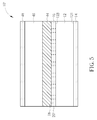
- FIG. 5 to FIG. 6 are schematic diagrams of the processes of the fabrication method of a touch-control display according to a second embodiment of the present invention.
- FIG. 7 is a schematic diagram of a sectional view of a touch-control display according to a third embodiment of the present invention.
- FIG. 1 to FIG. 2 are schematic diagrams showing the processes of the fabrication method of a touch-control display according to a first embodiment of the present invention.
- a first substrate 12 with transparency is first provided, wherein the first surface 121 and the second surface 123 are at two opposite sides of the first substrate 12 respectively.
- a first transparent conductive layer 14 and a second transparent conductive layer 16 are disposed on the first surface 121 and the second surface 123 respectively.
- the first substrate 12 may be a flexible substrate, such as a polyethylene terephthalate (PET) film, whose thickness may be about 125 micrometers ( ⁇ m), but not limited thereto. In other embodiments, the first substrate 12 may be a glass substrate whose thickness may be about 300 ⁇ m, but not limited thereto.
- the first transparent conductive layer 14 and the second transparent conductive layer 16 may respectively be an indium tin oxide (ITO) film, an indium zinc oxide (IZO) film, an aluminum zinc oxide (AZO) film, an indium tin zinc oxide (ITZO) film, a zinc oxide (ZnO) film, or a titanium-doped ZnO (TZO) film, or may respectively include any other conductive materials with transparent property.
- ITO indium tin oxide
- IZO indium zinc oxide
- AZO aluminum zinc oxide
- ITZO indium tin zinc oxide
- ZnO zinc oxide
- TZO titanium-doped ZnO
- the first transparent conductive layer 14 and the second transparent conductive layer 16 may include the same or different materials, and their thickness may respectively be about 0.001 ⁇ m, but not limited thereto.
- the first transparent conductive layer 14 and the second transparent conductive layer 16 may be blanketly formed on the first surface 121 and the second surface 123 of the first substrate 12 respectively through coating or other processes.
- a patterning process is performed to the second transparent conductive layer 16 to form a plurality of sensors 18 in the second transparent conductive layer 16 such that the patterned second transparent conductive layer 16 has a plurality of sensors 18 to serve as a sensor layer 20 of a touch panel 22 .
- the shapes and relative locations in the sensor layer 20 of the sensors 18 is not limited in the present invention, thus the dotted lines are used to represent the plural sensors 18 in the second transparent conductive layer 16 in FIG. 1 .
- the touch panel 22 has only one layer of the sensor layer 20 , such that the sensors 18 in the second transparent conductive layer 16 may include, for example, the first sensor series and the second sensor series extending along a first direction and a second direction respectively, wherein the first and second sensor series isolatedly cross to each other on the second surface 123 .
- the fabrication method in this embodiment may selectively further include a bridging process to electrically connect the sensors 18 in each of the first sensor series along the first direction or the second sensor series along the second direction, but not limited thereto.
- the sensors 18 of this embodiment may only extend along one single direction.
- the sensors 18 may have triangle-like shapes or have any structure and arrangement of various types of single layer sensors.
- a protection layer (not shown) may then be selectively formed on the surface of the second transparent conductive layer 16 to cover the second transparent conductive layer 16 .
- an adhesive layer 24 may also be used to attach an anti-glare layer 26 onto the side of the first substrate 12 having the second transparent conductive layer 16 to cover the second transparent conductive layer 16 .
- the adhesive layer 24 may be an optical clear adhesive (OCA) with a thickness of about 100 ⁇ m or less than 100 ⁇ m as an example, and the thickness of the anti-glare layer 26 may be about 100 ⁇ m for example.
- OCA optical clear adhesive
- the touch panel 22 of the present invention touch-control display 10 may include one single layer of sensor layer 20 , an adhesive layer 24 and an anti-glare layer 26 .
- the anti-glare layer 26 or the protection layer on the sensor layer 20 may be omitted.
- a display medium layer 28 and a display electrode layer 30 are successively formed on a side of the first transparent conductive layer 14 opposite to the first substrate 12 such that the first transparent conductive layer 14 , the display medium layer 28 and the display electrode layer 30 compose a display panel 32 .
- the display panel 32 may be an electrophoretic display panel, wherein the display medium layer 28 is an electrophoretic display layer, the first transparent conductive layer 14 serves as the common electrode layer of the display panel 32 , and the display electrode layer 30 may include a plurality of switch elements or pixel electrodes for controlling the gray level performance of the display panel 32 .
- the display panel 32 may be other types of display panels.
- the display medium layer may be a liquid crystal layer or an organic light emitting layer, but not limited thereto.
- the formation of the display medium layer 28 may be performed by a roll-to-roll process, as shown in FIG. 3 .
- a micro-cup material 34 may be formed on the side of the first substrate 12 having the first transparent conductive layer 14 through a coating process for instance.
- the micro-cup structures 38 arranged as an array may be embossed on the surface of the micro-cup material 34 by an embossing roller 36 through a micro-embossing process.
- the electrophoretic material 40 is filled into the micro-cup structures and then the micro-cup structures 38 filled with the electrophoretic material 40 are sealed.
- the seal layer is formed on the surfaces of the openings of the micro-cup structures 38 , as shown in FIG. 3 .
- a display electrode layer 30 with elements and pixel electrodes may be formed on the surfaces of the micro-cup structures 38 through roll-to-roll method in order to fabricate the display panel 32 .
- a cutting process may be adopted to cut the first substrate 12 into several portion with desired sizes to complete the fabrication of the present invention touch-control display 10 .
- the present invention touch-control display 10 fabricated through the above-mentioned method includes a first substrate 12 , a display panel 32 and a touch panel 22 .
- the display panel 32 and the touch panel 22 are respectively disposed on two opposite sides of the first substrate 12 .
- the display panel 32 and the touch panel 22 are disposed on the first surface 121 and the second surface 123 of the first substrate 12 respectively.
- the display panel 32 includes a first transparent conductive layer 14 which is disposed on the first surface 121 of the first substrate 12 and directly in contact with the first surface 121 of the first substrate 12 , wherein the first transparent conductive layer 14 may serve as the common electrode of the display panel 32 .
- the display panel 32 may further include a display medium layer 28 and a display electrode layer 30 .
- the display medium layer 28 is disposed on a side of the first transparent conductive layer 14 opposite to the first substrate 12
- the display electrode layer 30 is disposed on a side of the display medium layer 28 opposite to the first transparent conductive layer 14 .
- the first substrate 12 may be considered as a part of the display panel 32 , as shown in FIG. 2 .
- the touch panel 22 includes a second transparent conductive layer 16 which is disposed on the second surface 123 of the first substrate 12 and directly in contact with the first substrate 12 , wherein the second transparent conductive layer 16 serves as the sensor layer 20 of the touch panel 22 .
- the first transparent conductive layer 14 on the first surface 121 of the first substrate 12 is used as the common electrode of the display panel 32
- the second transparent conductive layer 16 on the second surface 123 of the first substrate 12 is used as the sensor layer 20 of the touch panel 22 . Therefore, an additional adhesive layer for fixing the separate touch panel to the display panel in a conventional touch-control display structure is not required anymore. As a result, at least the thickness of the adhesive layer (about 50 ⁇ m to 200 ⁇ m) and one of the substrates of the touch panel and the display panel can be saved.
- the touch panel may be formed on an additional PET substrate that is attached on the display panel, and the thickness of a PET substrate may be about 125 ⁇ m or more, for instance.
- the touch panel may be formed on a glass substrate, whose thickness may be reach 300 ⁇ m or more, in a conventional touch-control display. Therefore, according to the touch-control display structure of the first embodiment of the present invention and related fabrication method, a thickness of 200 ⁇ m or more than 200 ⁇ m may be saved in contrast to the conventional touch-control display, thus the material cost can be saved too. Furthermore, to reduce the numbers of substrates and films can also improve the light transmittance efficiency of the display panel 32 and the display performance.
- the touch-control display and the fabrication method thereof are not limited by the aforementioned embodiment, and may have other different preferred embodiments and variant embodiments.
- the identical components in each of the following embodiments and variant embodiments are marked with identical symbols.
- the following description will detail the dissimilarities among different embodiments and the identical features will not be redundantly described.
- FIG. 4 is a schematic diagram of a structure of a touch-control display 10 ′ according to a variant embodiment of the first embodiment of the present invention.
- the touch panel 22 ′ of the touch-control display 10 ′ does not include the above-mentioned adhesive layer and anti-glare layer on its surface.
- a slit coating process or other process may be adopted to form a protection layer 50 on the surface of the sensor layer 20 , wherein the protection layer 50 includes transparent insulating material and preferably has a greater hardness in order to provide a protection function for the touch-control display 10 ′.
- the thickness of the protection layer 50 may be about 1 ⁇ m to 20 ⁇ m for example.
- the protection layer 50 may be formed on the surface of the second transparent conductive layer 16 after the patterning process of the second transparent conductive layer 16 is performed.
- the protection layer 50 can be formed after the display panel 32 is fabricated.
- FIG. 5 to FIG. 6 are schematic diagrams of the processes of the fabrication method of a touch-control display according to a second embodiment of the present invention.
- the touch panel 22 ′ of the touch-control display 10 ′ has two sensor layers.
- a patterning process to the second transparent conductive layer 16 is performed to form a plurality of sensors 18 in the second transparent conductive layer 16 for manufacturing a first sensor layer, the sensor layer 20 ′.
- a second substrate 46 with a third transparent conductive layer 48 thereon is selectively fixed on the surface of the second transparent conductive layer 16 opposite to the first substrate 12 by an adhesive layer 44 .
- the second substrate 46 may be a glass substrate or a flexible substrate and may have a thickness of about 125 ⁇ m to about 300 ⁇ m, for example.
- the adhesive layer 44 may be an optical clear adhesive and have a thickness of about 50 ⁇ m, for example.
- the third transparent conductive layer 48 on the surface of the second substrate 46 can be patterned to form sensors in advance and then attached onto the second transparent conductive layer 16 .
- the third transparent conductive layer 48 may be fabricated on the second transparent conductive layer 16 through other process to replace being formed on the surface of the second substrate 46 in this embodiment.
- the anti-glare layer 26 may be selectively attached onto the third transparent conductive layer 48 by using the adhesive layer 24 , such that the second transparent conductive layer 16 , the adhesive layer 44 , the second substrate 46 , the third transparent conductive layer 48 , the adhesive layer 24 and the anti-glare layer 26 compose the touch panel 22 ′.
- the display medium layer 28 and the display electrode layer 30 are successively formed, such that the first transparent conductive layer 14 , the display medium layer 28 and the display electrode layer 30 compose a display panel 32 , wherein the first transparent conductive layer 14 serves as the common electrode of the display panel 32 .
- FIG. 7 is a schematic diagram of a sectional view of a touch-control display according to a third embodiment of the present invention.
- the two transparent conductive layers on two sides of the transparent substrate respectively serve as the common electrode and the shielding layer of the display panel.
- the touch-control display 100 of this embodiment includes a display panel 118 and a touch panel 120 .
- the display panel 118 includes a first substrate 112 , a first transparent conductive layer 114 and a second transparent conductive layer 116 , wherein the first transparent conductive layer 114 and the second transparent conductive layer 116 are disposed on the first surface 1121 and the second surface 1123 of the first substrate 112 respectively.
- the first substrate 112 may be a flexible substrate or a glass substrate.
- the first transparent conductive layer 114 and the second transparent conductive layer 116 may include materials of ITO, IZO, AZO, ITZO, ZnO, TZO, a combination of the above-mentioned materials, or any other transparent conductive material. Furthermore, the first transparent conductive layer 114 and the second transparent conductive layer 116 may have the same or different materials.
- the display panel 118 further includes a display medium layer 122 and a display electrode layer 124 disposed on the surface of the first transparent conductive layer 114 in order. The first transparent conductive layer 114 may serve as the common electrode of the display panel 118 .
- the display medium layer 122 may be any kind of display materials, such as an electrophoretic layer, a liquid crystal layer, and an organic light emitting layer, but not limited thereto.
- the touch panel 120 can be fixed on the display panel 118 by selectively attaching the second substrate 128 onto the surface of the second transparent conductive layer 116 through an adhesive layer 126 , wherein a third transparent conductive layer 130 is disposed on the second substrate 128 .
- the third transparent conductive layer 130 may serve as the sensor layer of the touch panel 120 and include a plurality of sensors 132 .
- the touch panel 120 may selectively include an anti-glare layer 134 attached on the surface of the third transparent conductive layer 130 by an adhesive layer 136 .
- the touch panel 120 of this embodiment only has one layer of touch-control element layer, includes the first sensor series extending along a first direction and the second sensor series extending along the second direction that isolated from and cross each other, for example.
- a plurality of bridge lines may be selectively formed on the surface of the third transparent conductive layer 130 such that the sensors 132 in each first sensor series along the first direction or each second sensor series along second direction are electrically connected to each other, but not limited thereto.
- the sensors 132 of this embodiment may only include the sensor series extending along one single direction, such as the sensor series with triangle-like shapes or other various structures and arrangements of one-layer touch-control element.
- the touch panel 120 may include two sensor layers, whose structures and relative arrangements may be as the two sensor layers, the second transparent conductive layer 16 and the third transparent conductive layer 48 , shown in FIG. 6 , but not limited thereto.
- the second transparent conductive layer 116 serves as the shielding layer of the display panel 118 .
- the second transparent conductive layer 116 may be floating, grounded, or be applied with a specific voltage, wherein the specific voltage is preferably less than or equal to the maximum driving voltage of the display panel 118 and greater than or equal to the minimum driving voltage of the display panel 118 .
- the second transparent conductive layer 116 serving as the shielding layer can reduce the capacitance formed between the conductive elements of the touch panel 120 and the display panel 118 , so as to improve the sensing performance of the touch panel 120 and reduce the noise of the display panel 118 .
- the fabrication method of the touch-control display 100 includes providing a first substrate 112 that has the second transparent conductive layer 116 and the first transparent conductive layer 114 disposed on two opposite surfaces of the first substrate 112 respectively, and then successively forming the display medium layer 122 and the display electrode layer 124 on the side of the first transparent conductive layer 114 opposite to the first substrate 112 such that the first transparent conductive layer 114 , the display medium layer 122 and the display electrode layer 124 compose the display panel 118 .
- a second substrate 128 is provided to be disposed on the second transparent conductive layer 116 , wherein the second substrate 128 has the third transparent conductive layer 130 disposed on the side of the second substrate 128 opposite to the second transparent conductive layer 116 . Then, a patterning process is performed to the third transparent conductive layer 130 to form sensors 132 in the third transparent conductive layer 130 . Therefore, the second substrate 128 and the third transparent conductive layer 130 compose the touch panel 120 .
- the patterning process to the third transparent conductive layer 130 may be performed before attaching the second substrate 128 onto the second transparent conductive layer 116 in other embodiments.
- an anti-glare layer 134 may be selectively attached to the third transparent conductive layer 130 by an adhesive layer 136 in this embodiment. It should be noted that the touch panel 120 may be fabricated before forming the display panel 118 in other embodiments.
- the two transparent conductive layers formed on two different sides of the first substrate are used as the electrode elements or devices of the touch panel and the display panel respectively; alternatively, one of the two transparent conductive layers is used as the shielding layer.
- at least one substrate and one adhesive layer are omitted in the present invention touch-control display save, such that the whole thickness of the apparatus can be effectively reduced and the light transmittance efficiency is raised.
- the transparent conductive layer is used as the shielding layer, the sensing performance of the touch panel and the display performance of the display panel can be improved at the same time.
Landscapes
- Engineering & Computer Science (AREA)
- Theoretical Computer Science (AREA)
- General Engineering & Computer Science (AREA)
- Human Computer Interaction (AREA)
- Physics & Mathematics (AREA)
- General Physics & Mathematics (AREA)
- Computer Hardware Design (AREA)
- Position Input By Displaying (AREA)
Applications Claiming Priority (3)
| Application Number | Priority Date | Filing Date | Title |
|---|---|---|---|
| TW102120965A | 2013-06-13 | ||
| TW102120965 | 2013-06-13 | ||
| TW102120965A TWI502429B (zh) | 2013-06-13 | 2013-06-13 | 觸控式顯示裝置及其製作方法 |
Publications (2)
| Publication Number | Publication Date |
|---|---|
| US20140368753A1 US20140368753A1 (en) | 2014-12-18 |
| US9582041B2 true US9582041B2 (en) | 2017-02-28 |
Family
ID=52018941
Family Applications (1)
| Application Number | Title | Priority Date | Filing Date |
|---|---|---|---|
| US14/288,411 Active US9582041B2 (en) | 2013-06-13 | 2014-05-28 | Touch-control display and fabrication method thereof |
Country Status (3)
| Country | Link |
|---|---|
| US (1) | US9582041B2 (zh) |
| CN (1) | CN104238804A (zh) |
| TW (1) | TWI502429B (zh) |
Cited By (14)
| Publication number | Priority date | Publication date | Assignee | Title |
|---|---|---|---|---|
| US10573257B2 (en) | 2017-05-30 | 2020-02-25 | E Ink Corporation | Electro-optic displays |
| US10824042B1 (en) | 2017-10-27 | 2020-11-03 | E Ink Corporation | Electro-optic display and composite materials having low thermal sensitivity for use therein |
| US10882042B2 (en) | 2017-10-18 | 2021-01-05 | E Ink Corporation | Digital microfluidic devices including dual substrates with thin-film transistors and capacitive sensing |
| US11016358B2 (en) | 2017-03-28 | 2021-05-25 | E Ink Corporation | Porous backplane for electro-optic display |
| US11145262B2 (en) | 2018-11-09 | 2021-10-12 | E Ink Corporation | Electro-optic displays |
| US11175561B1 (en) | 2018-04-12 | 2021-11-16 | E Ink Corporation | Electrophoretic display media with network electrodes and methods of making and using the same |
| US11353759B2 (en) | 2018-09-17 | 2022-06-07 | Nuclera Nucleics Ltd. | Backplanes with hexagonal and triangular electrodes |
| US11404013B2 (en) | 2017-05-30 | 2022-08-02 | E Ink Corporation | Electro-optic displays with resistors for discharging remnant charges |
| US11511096B2 (en) | 2018-10-15 | 2022-11-29 | E Ink Corporation | Digital microfluidic delivery device |
| US11513415B2 (en) | 2020-06-03 | 2022-11-29 | E Ink Corporation | Foldable electrophoretic display module including non-conductive support plate |
| US11521565B2 (en) | 2018-12-28 | 2022-12-06 | E Ink Corporation | Crosstalk reduction for electro-optic displays |
| US11537024B2 (en) | 2018-12-30 | 2022-12-27 | E Ink California, Llc | Electro-optic displays |
| US11830449B2 (en) | 2022-03-01 | 2023-11-28 | E Ink Corporation | Electro-optic displays |
| US11935495B2 (en) | 2021-08-18 | 2024-03-19 | E Ink Corporation | Methods for driving electro-optic displays |
Families Citing this family (12)
| Publication number | Priority date | Publication date | Assignee | Title |
|---|---|---|---|---|
| KR102211968B1 (ko) * | 2013-12-02 | 2021-02-05 | 삼성디스플레이 주식회사 | 터치 패널, 표시 장치 및 터치 패널의 제조 방법 |
| US10317767B2 (en) | 2014-02-07 | 2019-06-11 | E Ink Corporation | Electro-optic display backplane structure with drive components and pixel electrodes on opposed surfaces |
| CN105786230B (zh) * | 2014-12-23 | 2019-08-13 | 宸鸿科技(厦门)有限公司 | 触控面板及其制造方法 |
| CN105988627B (zh) * | 2015-02-25 | 2020-06-30 | 宸鸿科技(厦门)有限公司 | 触控显示装置及其制造方法 |
| CN104793821A (zh) * | 2015-04-20 | 2015-07-22 | 南昌欧菲光科技有限公司 | 触控面板及其制作方法 |
| CN106249501A (zh) * | 2015-06-08 | 2016-12-21 | 御智管理顾问有限公司 | 显示层结构、显示模块及其制作方法 |
| TWI604361B (zh) * | 2016-02-05 | 2017-11-01 | 速博思股份有限公司 | 具壓力觸覺功能之感測裝置 |
| WO2018160546A1 (en) | 2017-02-28 | 2018-09-07 | E Ink Corporation | Writeable electrophoretic displays including sensing circuits and styli configured to interact with sensing circuits |
| WO2018213687A2 (en) | 2017-05-19 | 2018-11-22 | E Ink Corporation | Foldable electro-optic display including digitization and touch sensing |
| CN107203298B (zh) * | 2017-05-26 | 2019-05-07 | 京东方科技集团股份有限公司 | 显示装置、触控显示面板及其驱动方法 |
| CN114327119B (zh) * | 2020-10-12 | 2024-08-06 | 瀚宇彩晶股份有限公司 | 触控面板 |
| CN114489368A (zh) * | 2020-11-13 | 2022-05-13 | 和鑫光电股份有限公司 | 双面触控面板及其制造方法 |
Citations (15)
| Publication number | Priority date | Publication date | Assignee | Title |
|---|---|---|---|---|
| US20080062148A1 (en) * | 2006-06-09 | 2008-03-13 | Hotelling Steve P | Touch screen liquid crystal display |
| US20080129317A1 (en) * | 2006-12-01 | 2008-06-05 | Katsuichi Oba | Input device and method of manufacturing the same |
| US20090180069A1 (en) | 2008-01-11 | 2009-07-16 | Epson Imaging Devices Corporation | Liquid crystal device and electronic apparatus |
| US20090273570A1 (en) * | 2008-04-30 | 2009-11-05 | Apple Inc. | Multi-touch sensor patterns and stack-ups |
| US20100052700A1 (en) | 2008-09-03 | 2010-03-04 | Rohm Co., Ltd. | Capacitive sensor |
| TW201116919A (en) | 2009-11-09 | 2011-05-16 | Innolux Display Corp | Display apparatus and touch display device |
| CN102262469A (zh) | 2010-05-25 | 2011-11-30 | 东莞万士达液晶显示器有限公司 | 触控面板、触控显示面板及触控面板的制作方法 |
| US8106324B2 (en) | 2008-02-21 | 2012-01-31 | Wintek Corporation | Touch panel and driving method of touch panel |
| TWI369534B (en) | 2008-02-26 | 2012-08-01 | Wintek Corp | Touch display, liquid crystal display with a built-in touch panel and fabricating method thereof |
| US20120242600A1 (en) * | 2011-03-24 | 2012-09-27 | Jeng-Maw Chiou | Touch operating display device |
| CN102736287A (zh) | 2011-03-29 | 2012-10-17 | 瀚宇彩晶股份有限公司 | 触控显示装置 |
| TWM443223U (en) | 2012-06-08 | 2012-12-11 | Giantplus Technology Co Ltd | Touch display panel |
| US20130057943A1 (en) | 2011-09-02 | 2013-03-07 | Shih Hua Technology Ltd. | Electronic paper display device |
| US20140124241A1 (en) * | 2012-11-08 | 2014-05-08 | Industrial Technology Research Institute | Touch structure and manufacturing method for the same |
| US20150220190A1 (en) * | 2012-09-11 | 2015-08-06 | Sharp Kabushiki Kaisha | Display apparatus |
Family Cites Families (1)
| Publication number | Priority date | Publication date | Assignee | Title |
|---|---|---|---|---|
| CN101447507A (zh) * | 2008-12-12 | 2009-06-03 | 信利半导体有限公司 | 一种具有触摸屏功能的有机电致发光显示器 |
-
2013
- 2013-06-13 TW TW102120965A patent/TWI502429B/zh active
- 2013-12-30 CN CN201310747093.XA patent/CN104238804A/zh active Pending
-
2014
- 2014-05-28 US US14/288,411 patent/US9582041B2/en active Active
Patent Citations (20)
| Publication number | Priority date | Publication date | Assignee | Title |
|---|---|---|---|---|
| US20080062148A1 (en) * | 2006-06-09 | 2008-03-13 | Hotelling Steve P | Touch screen liquid crystal display |
| US20080129317A1 (en) * | 2006-12-01 | 2008-06-05 | Katsuichi Oba | Input device and method of manufacturing the same |
| US20090180069A1 (en) | 2008-01-11 | 2009-07-16 | Epson Imaging Devices Corporation | Liquid crystal device and electronic apparatus |
| CN101533186A (zh) | 2008-01-11 | 2009-09-16 | 爱普生映像元器件有限公司 | 液晶装置及电子设备 |
| US8106324B2 (en) | 2008-02-21 | 2012-01-31 | Wintek Corporation | Touch panel and driving method of touch panel |
| TWI369534B (en) | 2008-02-26 | 2012-08-01 | Wintek Corp | Touch display, liquid crystal display with a built-in touch panel and fabricating method thereof |
| US20090273570A1 (en) * | 2008-04-30 | 2009-11-05 | Apple Inc. | Multi-touch sensor patterns and stack-ups |
| CN102016775A (zh) | 2008-04-30 | 2011-04-13 | 苹果公司 | 多点触摸传感器图案和叠层 |
| US20100052700A1 (en) | 2008-09-03 | 2010-03-04 | Rohm Co., Ltd. | Capacitive sensor |
| CN101666832A (zh) | 2008-09-03 | 2010-03-10 | 罗姆股份有限公司 | 静电电容传感器及其控制方法、检测电路、输入装置 |
| TW201116919A (en) | 2009-11-09 | 2011-05-16 | Innolux Display Corp | Display apparatus and touch display device |
| CN102262469A (zh) | 2010-05-25 | 2011-11-30 | 东莞万士达液晶显示器有限公司 | 触控面板、触控显示面板及触控面板的制作方法 |
| US20120242600A1 (en) * | 2011-03-24 | 2012-09-27 | Jeng-Maw Chiou | Touch operating display device |
| TW201239695A (en) | 2011-03-24 | 2012-10-01 | Hannstar Display Corp | Touch display device |
| CN102736287A (zh) | 2011-03-29 | 2012-10-17 | 瀚宇彩晶股份有限公司 | 触控显示装置 |
| US20130057943A1 (en) | 2011-09-02 | 2013-03-07 | Shih Hua Technology Ltd. | Electronic paper display device |
| TW201312243A (zh) | 2011-09-02 | 2013-03-16 | Shih Hua Technology Ltd | 觸控式電子紙顯示器 |
| TWM443223U (en) | 2012-06-08 | 2012-12-11 | Giantplus Technology Co Ltd | Touch display panel |
| US20150220190A1 (en) * | 2012-09-11 | 2015-08-06 | Sharp Kabushiki Kaisha | Display apparatus |
| US20140124241A1 (en) * | 2012-11-08 | 2014-05-08 | Industrial Technology Research Institute | Touch structure and manufacturing method for the same |
Cited By (20)
| Publication number | Priority date | Publication date | Assignee | Title |
|---|---|---|---|---|
| US11016358B2 (en) | 2017-03-28 | 2021-05-25 | E Ink Corporation | Porous backplane for electro-optic display |
| US11404013B2 (en) | 2017-05-30 | 2022-08-02 | E Ink Corporation | Electro-optic displays with resistors for discharging remnant charges |
| US10825405B2 (en) | 2017-05-30 | 2020-11-03 | E Ink Corporatior | Electro-optic displays |
| US11107425B2 (en) | 2017-05-30 | 2021-08-31 | E Ink Corporation | Electro-optic displays with resistors for discharging remnant charges |
| US10573257B2 (en) | 2017-05-30 | 2020-02-25 | E Ink Corporation | Electro-optic displays |
| US10882042B2 (en) | 2017-10-18 | 2021-01-05 | E Ink Corporation | Digital microfluidic devices including dual substrates with thin-film transistors and capacitive sensing |
| US10824042B1 (en) | 2017-10-27 | 2020-11-03 | E Ink Corporation | Electro-optic display and composite materials having low thermal sensitivity for use therein |
| US11656524B2 (en) | 2018-04-12 | 2023-05-23 | E Ink Corporation | Electrophoretic display media with network electrodes and methods of making and using the same |
| US11175561B1 (en) | 2018-04-12 | 2021-11-16 | E Ink Corporation | Electrophoretic display media with network electrodes and methods of making and using the same |
| US11353759B2 (en) | 2018-09-17 | 2022-06-07 | Nuclera Nucleics Ltd. | Backplanes with hexagonal and triangular electrodes |
| US11511096B2 (en) | 2018-10-15 | 2022-11-29 | E Ink Corporation | Digital microfluidic delivery device |
| US11450287B2 (en) | 2018-11-09 | 2022-09-20 | E Ink Corporation | Electro-optic displays |
| US11145262B2 (en) | 2018-11-09 | 2021-10-12 | E Ink Corporation | Electro-optic displays |
| US11521565B2 (en) | 2018-12-28 | 2022-12-06 | E Ink Corporation | Crosstalk reduction for electro-optic displays |
| US11537024B2 (en) | 2018-12-30 | 2022-12-27 | E Ink California, Llc | Electro-optic displays |
| US12032264B2 (en) | 2018-12-30 | 2024-07-09 | E Ink Corporation | Electro-optic displays |
| US11513415B2 (en) | 2020-06-03 | 2022-11-29 | E Ink Corporation | Foldable electrophoretic display module including non-conductive support plate |
| US11874580B2 (en) | 2020-06-03 | 2024-01-16 | E Ink Corporation | Foldable electrophoretic display module including non-conductive support plate |
| US11935495B2 (en) | 2021-08-18 | 2024-03-19 | E Ink Corporation | Methods for driving electro-optic displays |
| US11830449B2 (en) | 2022-03-01 | 2023-11-28 | E Ink Corporation | Electro-optic displays |
Also Published As
| Publication number | Publication date |
|---|---|
| CN104238804A (zh) | 2014-12-24 |
| US20140368753A1 (en) | 2014-12-18 |
| TWI502429B (zh) | 2015-10-01 |
| TW201447665A (zh) | 2014-12-16 |
Similar Documents
| Publication | Publication Date | Title |
|---|---|---|
| US9582041B2 (en) | Touch-control display and fabrication method thereof | |
| EP3696646B1 (en) | Display device and method of manufacturing the same | |
| US9383850B2 (en) | Touch screen and manufacturing method | |
| US9207819B2 (en) | Touch sensing display panel and touch sensing liquid crystal display panel | |
| US10216332B2 (en) | Color filter substrate and in-cell touch display device | |
| TWI443564B (zh) | Input device and manufacturing method thereof | |
| US8994677B2 (en) | Touch sensing structure | |
| US8933900B2 (en) | Input device and method of manufacturing the same | |
| TWI477853B (zh) | 觸控面板及其製造方法 | |
| US20160370904A1 (en) | Color filter substrate, array substrate and display device | |
| US20110254778A1 (en) | Slim type touch device | |
| US9921674B2 (en) | Touch-sensing liquid crystal display panel | |
| US20140049892A1 (en) | Touch panel and touch display panel | |
| US9207483B2 (en) | In-cell touch display panel structure with metal layer on lower substrate for sensing | |
| US20150362949A1 (en) | Touch display device and touch substrate | |
| US20160342271A1 (en) | Touch Screen and Method for Manufacturing the Same | |
| US20150029422A1 (en) | Touch panel and touch display panel | |
| TW201928624A (zh) | 觸控顯示面板 | |
| CN105094394A (zh) | 触控显示面板 | |
| US20090321147A1 (en) | Touch panel with patterned layer | |
| JP2010079734A (ja) | 静電容量型タッチパネル | |
| KR20150007107A (ko) | 터치센서 | |
| US9411448B2 (en) | Touch display apparatus | |
| CN203909742U (zh) | 触控显示面板 | |
| KR101328763B1 (ko) | 터치스크린용 투명 회로 기판 및 그 제조 방법 |
Legal Events
| Date | Code | Title | Description |
|---|---|---|---|
| AS | Assignment |
Owner name: SIPIX TECHNOLOGY, INC., TAIWAN Free format text: ASSIGNMENT OF ASSIGNORS INTEREST;ASSIGNORS:CHENG, HSIAO-LUNG;HUNG, CHI-MAO;SUN, WEI-MIN;AND OTHERS;REEL/FRAME:032970/0654 Effective date: 20140124 |
|
| STCF | Information on status: patent grant |
Free format text: PATENTED CASE |
|
| AS | Assignment |
Owner name: YUANHAN MATERIALS INC., TAIWAN Free format text: MERGER AND CHANGE OF NAME;ASSIGNORS:SIPIX TECHNOLOGY INC.;YUANHAN MATERIALS INC.;REEL/FRAME:052944/0912 Effective date: 20191001 |
|
| MAFP | Maintenance fee payment |
Free format text: PAYMENT OF MAINTENANCE FEE, 4TH YEAR, LARGE ENTITY (ORIGINAL EVENT CODE: M1551); ENTITY STATUS OF PATENT OWNER: LARGE ENTITY Year of fee payment: 4 |
|
| MAFP | Maintenance fee payment |
Free format text: PAYMENT OF MAINTENANCE FEE, 8TH YEAR, LARGE ENTITY (ORIGINAL EVENT CODE: M1552); ENTITY STATUS OF PATENT OWNER: LARGE ENTITY Year of fee payment: 8 |