US9564738B2 - Semiconductor laser device and manufacturing method thereof - Google Patents
Semiconductor laser device and manufacturing method thereof Download PDFInfo
- Publication number
- US9564738B2 US9564738B2 US14/932,010 US201514932010A US9564738B2 US 9564738 B2 US9564738 B2 US 9564738B2 US 201514932010 A US201514932010 A US 201514932010A US 9564738 B2 US9564738 B2 US 9564738B2
- Authority
- US
- United States
- Prior art keywords
- layer
- type clad
- type
- clad layer
- current
- Prior art date
- Legal status (The legal status is an assumption and is not a legal conclusion. Google has not performed a legal analysis and makes no representation as to the accuracy of the status listed.)
- Active
Links
Images


Classifications
-
- H—ELECTRICITY
- H01—ELECTRIC ELEMENTS
- H01S—DEVICES USING THE PROCESS OF LIGHT AMPLIFICATION BY STIMULATED EMISSION OF RADIATION [LASER] TO AMPLIFY OR GENERATE LIGHT; DEVICES USING STIMULATED EMISSION OF ELECTROMAGNETIC RADIATION IN WAVE RANGES OTHER THAN OPTICAL
- H01S5/00—Semiconductor lasers
- H01S5/30—Structure or shape of the active region; Materials used for the active region
- H01S5/34—Structure or shape of the active region; Materials used for the active region comprising quantum well or superlattice structures, e.g. single quantum well [SQW] lasers, multiple quantum well [MQW] lasers or graded index separate confinement heterostructure [GRINSCH] lasers
- H01S5/343—Structure or shape of the active region; Materials used for the active region comprising quantum well or superlattice structures, e.g. single quantum well [SQW] lasers, multiple quantum well [MQW] lasers or graded index separate confinement heterostructure [GRINSCH] lasers in AIIIBV compounds, e.g. AlGaAs-laser, InP-based laser
- H01S5/3434—Structure or shape of the active region; Materials used for the active region comprising quantum well or superlattice structures, e.g. single quantum well [SQW] lasers, multiple quantum well [MQW] lasers or graded index separate confinement heterostructure [GRINSCH] lasers in AIIIBV compounds, e.g. AlGaAs-laser, InP-based laser with a well layer comprising at least both As and P as V-compounds
-
- B—PERFORMING OPERATIONS; TRANSPORTING
- B82—NANOTECHNOLOGY
- B82Y—SPECIFIC USES OR APPLICATIONS OF NANOSTRUCTURES; MEASUREMENT OR ANALYSIS OF NANOSTRUCTURES; MANUFACTURE OR TREATMENT OF NANOSTRUCTURES
- B82Y20/00—Nanooptics, e.g. quantum optics or photonic crystals
-
- H—ELECTRICITY
- H01—ELECTRIC ELEMENTS
- H01S—DEVICES USING THE PROCESS OF LIGHT AMPLIFICATION BY STIMULATED EMISSION OF RADIATION [LASER] TO AMPLIFY OR GENERATE LIGHT; DEVICES USING STIMULATED EMISSION OF ELECTROMAGNETIC RADIATION IN WAVE RANGES OTHER THAN OPTICAL
- H01S5/00—Semiconductor lasers
- H01S5/20—Structure or shape of the semiconductor body to guide the optical wave ; Confining structures perpendicular to the optical axis, e.g. index or gain guiding, stripe geometry, broad area lasers, gain tailoring, transverse or lateral reflectors, special cladding structures, MQW barrier reflection layers
- H01S5/22—Structure or shape of the semiconductor body to guide the optical wave ; Confining structures perpendicular to the optical axis, e.g. index or gain guiding, stripe geometry, broad area lasers, gain tailoring, transverse or lateral reflectors, special cladding structures, MQW barrier reflection layers having a ridge or stripe structure
- H01S5/2205—Structure or shape of the semiconductor body to guide the optical wave ; Confining structures perpendicular to the optical axis, e.g. index or gain guiding, stripe geometry, broad area lasers, gain tailoring, transverse or lateral reflectors, special cladding structures, MQW barrier reflection layers having a ridge or stripe structure comprising special burying or current confinement layers
- H01S5/2206—Structure or shape of the semiconductor body to guide the optical wave ; Confining structures perpendicular to the optical axis, e.g. index or gain guiding, stripe geometry, broad area lasers, gain tailoring, transverse or lateral reflectors, special cladding structures, MQW barrier reflection layers having a ridge or stripe structure comprising special burying or current confinement layers based on III-V materials
- H01S5/2209—GaInP based
-
- H—ELECTRICITY
- H01—ELECTRIC ELEMENTS
- H01S—DEVICES USING THE PROCESS OF LIGHT AMPLIFICATION BY STIMULATED EMISSION OF RADIATION [LASER] TO AMPLIFY OR GENERATE LIGHT; DEVICES USING STIMULATED EMISSION OF ELECTROMAGNETIC RADIATION IN WAVE RANGES OTHER THAN OPTICAL
- H01S5/00—Semiconductor lasers
- H01S5/20—Structure or shape of the semiconductor body to guide the optical wave ; Confining structures perpendicular to the optical axis, e.g. index or gain guiding, stripe geometry, broad area lasers, gain tailoring, transverse or lateral reflectors, special cladding structures, MQW barrier reflection layers
- H01S5/22—Structure or shape of the semiconductor body to guide the optical wave ; Confining structures perpendicular to the optical axis, e.g. index or gain guiding, stripe geometry, broad area lasers, gain tailoring, transverse or lateral reflectors, special cladding structures, MQW barrier reflection layers having a ridge or stripe structure
- H01S5/2205—Structure or shape of the semiconductor body to guide the optical wave ; Confining structures perpendicular to the optical axis, e.g. index or gain guiding, stripe geometry, broad area lasers, gain tailoring, transverse or lateral reflectors, special cladding structures, MQW barrier reflection layers having a ridge or stripe structure comprising special burying or current confinement layers
- H01S5/2206—Structure or shape of the semiconductor body to guide the optical wave ; Confining structures perpendicular to the optical axis, e.g. index or gain guiding, stripe geometry, broad area lasers, gain tailoring, transverse or lateral reflectors, special cladding structures, MQW barrier reflection layers having a ridge or stripe structure comprising special burying or current confinement layers based on III-V materials
- H01S5/221—Structure or shape of the semiconductor body to guide the optical wave ; Confining structures perpendicular to the optical axis, e.g. index or gain guiding, stripe geometry, broad area lasers, gain tailoring, transverse or lateral reflectors, special cladding structures, MQW barrier reflection layers having a ridge or stripe structure comprising special burying or current confinement layers based on III-V materials containing aluminium
-
- H—ELECTRICITY
- H01—ELECTRIC ELEMENTS
- H01S—DEVICES USING THE PROCESS OF LIGHT AMPLIFICATION BY STIMULATED EMISSION OF RADIATION [LASER] TO AMPLIFY OR GENERATE LIGHT; DEVICES USING STIMULATED EMISSION OF ELECTROMAGNETIC RADIATION IN WAVE RANGES OTHER THAN OPTICAL
- H01S5/00—Semiconductor lasers
- H01S5/30—Structure or shape of the active region; Materials used for the active region
- H01S5/32—Structure or shape of the active region; Materials used for the active region comprising PN junctions, e.g. hetero- or double- heterostructures
- H01S5/3211—Structure or shape of the active region; Materials used for the active region comprising PN junctions, e.g. hetero- or double- heterostructures characterised by special cladding layers, e.g. details on band-discontinuities
- H01S5/3213—Structure or shape of the active region; Materials used for the active region comprising PN junctions, e.g. hetero- or double- heterostructures characterised by special cladding layers, e.g. details on band-discontinuities asymmetric clading layers
-
- H—ELECTRICITY
- H01—ELECTRIC ELEMENTS
- H01S—DEVICES USING THE PROCESS OF LIGHT AMPLIFICATION BY STIMULATED EMISSION OF RADIATION [LASER] TO AMPLIFY OR GENERATE LIGHT; DEVICES USING STIMULATED EMISSION OF ELECTROMAGNETIC RADIATION IN WAVE RANGES OTHER THAN OPTICAL
- H01S5/00—Semiconductor lasers
- H01S5/30—Structure or shape of the active region; Materials used for the active region
- H01S5/34—Structure or shape of the active region; Materials used for the active region comprising quantum well or superlattice structures, e.g. single quantum well [SQW] lasers, multiple quantum well [MQW] lasers or graded index separate confinement heterostructure [GRINSCH] lasers
- H01S5/3403—Structure or shape of the active region; Materials used for the active region comprising quantum well or superlattice structures, e.g. single quantum well [SQW] lasers, multiple quantum well [MQW] lasers or graded index separate confinement heterostructure [GRINSCH] lasers having a strained layer structure in which the strain performs a special function, e.g. general strain effects, strain versus polarisation
- H01S5/3404—Structure or shape of the active region; Materials used for the active region comprising quantum well or superlattice structures, e.g. single quantum well [SQW] lasers, multiple quantum well [MQW] lasers or graded index separate confinement heterostructure [GRINSCH] lasers having a strained layer structure in which the strain performs a special function, e.g. general strain effects, strain versus polarisation influencing the polarisation
-
- H—ELECTRICITY
- H01—ELECTRIC ELEMENTS
- H01S—DEVICES USING THE PROCESS OF LIGHT AMPLIFICATION BY STIMULATED EMISSION OF RADIATION [LASER] TO AMPLIFY OR GENERATE LIGHT; DEVICES USING STIMULATED EMISSION OF ELECTROMAGNETIC RADIATION IN WAVE RANGES OTHER THAN OPTICAL
- H01S5/00—Semiconductor lasers
- H01S5/30—Structure or shape of the active region; Materials used for the active region
- H01S5/34—Structure or shape of the active region; Materials used for the active region comprising quantum well or superlattice structures, e.g. single quantum well [SQW] lasers, multiple quantum well [MQW] lasers or graded index separate confinement heterostructure [GRINSCH] lasers
- H01S5/343—Structure or shape of the active region; Materials used for the active region comprising quantum well or superlattice structures, e.g. single quantum well [SQW] lasers, multiple quantum well [MQW] lasers or graded index separate confinement heterostructure [GRINSCH] lasers in AIIIBV compounds, e.g. AlGaAs-laser, InP-based laser
- H01S5/34326—Structure or shape of the active region; Materials used for the active region comprising quantum well or superlattice structures, e.g. single quantum well [SQW] lasers, multiple quantum well [MQW] lasers or graded index separate confinement heterostructure [GRINSCH] lasers in AIIIBV compounds, e.g. AlGaAs-laser, InP-based laser with a well layer based on InGa(Al)P, e.g. red laser
-
- G—PHYSICS
- G11—INFORMATION STORAGE
- G11B—INFORMATION STORAGE BASED ON RELATIVE MOVEMENT BETWEEN RECORD CARRIER AND TRANSDUCER
- G11B5/00—Recording by magnetisation or demagnetisation of a record carrier; Reproducing by magnetic means; Record carriers therefor
- G11B2005/0002—Special dispositions or recording techniques
- G11B2005/0005—Arrangements, methods or circuits
- G11B2005/0021—Thermally assisted recording using an auxiliary energy source for heating the recording layer locally to assist the magnetization reversal
-
- H—ELECTRICITY
- H01—ELECTRIC ELEMENTS
- H01S—DEVICES USING THE PROCESS OF LIGHT AMPLIFICATION BY STIMULATED EMISSION OF RADIATION [LASER] TO AMPLIFY OR GENERATE LIGHT; DEVICES USING STIMULATED EMISSION OF ELECTROMAGNETIC RADIATION IN WAVE RANGES OTHER THAN OPTICAL
- H01S2301/00—Functional characteristics
- H01S2301/14—Semiconductor lasers with special structural design for lasing in a specific polarisation mode
- H01S2301/145—TM polarisation
-
- H—ELECTRICITY
- H01—ELECTRIC ELEMENTS
- H01S—DEVICES USING THE PROCESS OF LIGHT AMPLIFICATION BY STIMULATED EMISSION OF RADIATION [LASER] TO AMPLIFY OR GENERATE LIGHT; DEVICES USING STIMULATED EMISSION OF ELECTROMAGNETIC RADIATION IN WAVE RANGES OTHER THAN OPTICAL
- H01S2301/00—Functional characteristics
- H01S2301/17—Semiconductor lasers comprising special layers
- H01S2301/173—The laser chip comprising special buffer layers, e.g. dislocation prevention or reduction
-
- H—ELECTRICITY
- H01—ELECTRIC ELEMENTS
- H01S—DEVICES USING THE PROCESS OF LIGHT AMPLIFICATION BY STIMULATED EMISSION OF RADIATION [LASER] TO AMPLIFY OR GENERATE LIGHT; DEVICES USING STIMULATED EMISSION OF ELECTROMAGNETIC RADIATION IN WAVE RANGES OTHER THAN OPTICAL
- H01S5/00—Semiconductor lasers
- H01S5/10—Construction or shape of the optical resonator, e.g. extended or external cavity, coupled cavities, bent-guide, varying width, thickness or composition of the active region
- H01S5/16—Window-type lasers, i.e. with a region of non-absorbing material between the active region and the reflecting surface
-
- H—ELECTRICITY
- H01—ELECTRIC ELEMENTS
- H01S—DEVICES USING THE PROCESS OF LIGHT AMPLIFICATION BY STIMULATED EMISSION OF RADIATION [LASER] TO AMPLIFY OR GENERATE LIGHT; DEVICES USING STIMULATED EMISSION OF ELECTROMAGNETIC RADIATION IN WAVE RANGES OTHER THAN OPTICAL
- H01S5/00—Semiconductor lasers
- H01S5/20—Structure or shape of the semiconductor body to guide the optical wave ; Confining structures perpendicular to the optical axis, e.g. index or gain guiding, stripe geometry, broad area lasers, gain tailoring, transverse or lateral reflectors, special cladding structures, MQW barrier reflection layers
- H01S5/22—Structure or shape of the semiconductor body to guide the optical wave ; Confining structures perpendicular to the optical axis, e.g. index or gain guiding, stripe geometry, broad area lasers, gain tailoring, transverse or lateral reflectors, special cladding structures, MQW barrier reflection layers having a ridge or stripe structure
-
- H—ELECTRICITY
- H01—ELECTRIC ELEMENTS
- H01S—DEVICES USING THE PROCESS OF LIGHT AMPLIFICATION BY STIMULATED EMISSION OF RADIATION [LASER] TO AMPLIFY OR GENERATE LIGHT; DEVICES USING STIMULATED EMISSION OF ELECTROMAGNETIC RADIATION IN WAVE RANGES OTHER THAN OPTICAL
- H01S5/00—Semiconductor lasers
- H01S5/30—Structure or shape of the active region; Materials used for the active region
- H01S5/32—Structure or shape of the active region; Materials used for the active region comprising PN junctions, e.g. hetero- or double- heterostructures
- H01S5/3202—Structure or shape of the active region; Materials used for the active region comprising PN junctions, e.g. hetero- or double- heterostructures grown on specifically orientated substrates, or using orientation dependent growth
-
- H—ELECTRICITY
- H01—ELECTRIC ELEMENTS
- H01S—DEVICES USING THE PROCESS OF LIGHT AMPLIFICATION BY STIMULATED EMISSION OF RADIATION [LASER] TO AMPLIFY OR GENERATE LIGHT; DEVICES USING STIMULATED EMISSION OF ELECTROMAGNETIC RADIATION IN WAVE RANGES OTHER THAN OPTICAL
- H01S5/00—Semiconductor lasers
- H01S5/30—Structure or shape of the active region; Materials used for the active region
- H01S5/34—Structure or shape of the active region; Materials used for the active region comprising quantum well or superlattice structures, e.g. single quantum well [SQW] lasers, multiple quantum well [MQW] lasers or graded index separate confinement heterostructure [GRINSCH] lasers
- H01S5/343—Structure or shape of the active region; Materials used for the active region comprising quantum well or superlattice structures, e.g. single quantum well [SQW] lasers, multiple quantum well [MQW] lasers or graded index separate confinement heterostructure [GRINSCH] lasers in AIIIBV compounds, e.g. AlGaAs-laser, InP-based laser
- H01S5/34313—Structure or shape of the active region; Materials used for the active region comprising quantum well or superlattice structures, e.g. single quantum well [SQW] lasers, multiple quantum well [MQW] lasers or graded index separate confinement heterostructure [GRINSCH] lasers in AIIIBV compounds, e.g. AlGaAs-laser, InP-based laser with a well layer having only As as V-compound, e.g. AlGaAs, InGaAs
Definitions
- the present disclosure(s) relate to a semiconductor laser device and a manufacturing method thereof.
- the present disclosure(s) include some embodiments of a semiconductor laser device capable of obtaining TM-mode oscillation. Moreover, the present disclosure(s) include some embodiments of a semiconductor laser device which is suitable for large output purposes and capable of obtaining stable TM-mode oscillation.
- the “heat-assisted recording” method refers to a method in which, using a laser diode (semiconductor laser device) as a heat source, a force for holding magnetic fields is temporarily weakened and a writing task is performed in that state.
- a semiconductor laser device used in a recording device of “heat-assisted recording” types need to generate a large output despite its small chip size. Since a restriction is imposed on the mounting space of the semiconductor laser device, it is sometimes necessary to realize not only TE (Transverse Electric) polarization, but also TM (Transverse Magnetic) polarization.
- a semiconductor laser device includes a p-type clad layer and an n-type clad layer, a p-side guide layer and an n-side guide layer, and an active layer.
- the p-side guide layer and the n-side guide layer are interposed between the p-type clad layer and the n-type clad layer.
- the active layer is interposed between the p-side guide layer and the n-side guide layer.
- the active layer includes at least two quantum well layers and a barrier layer interposed between the quantum well layers adjoining to each other.
- Each of the p-type clad layer and the n-type clad layer is formed of a (Al x1 Ga (1-x1) ) 0.51 In 0.49 P layer (0 ⁇ x1 ⁇ 1).
- Each of the p-side guide layer, the n-side guide layer and the barrier layer is formed of an Al x2 Ga (1-x2) As layer (0 ⁇ x2 ⁇ 1).
- Each of the quantum well layers is formed of a GaAs (1-x3) P x3 layer (0 ⁇ x3 ⁇ 1).
- the (Al x1 Ga (1-x1) ) 0.51 In 0.49 P layer has a composition, where x1>0.7, and the Al x2 Ga (1-x2) As layer having a composition, where 0.4 ⁇ x2 ⁇ 0.8.
- each of the p-type clad layer and the n-type clad layer is formed of a (Al x1 Ga (1-x1) ) 0.51 In 0.49 P layer (0 ⁇ x1 ⁇ 1) while each of the p-side guide layer and the n-side guide layer is formed of a Al x2 Ga (1-x2) As layer (0 ⁇ x2 ⁇ 1). It is therefore possible to increase the band gap difference between the clad layers and the guide layers. Since the clad layers and the guide layers are formed of materials differing in self-diffusing coefficient from each other, it is possible to make different the diffusing velocity of carriers in the clad layers and the diffusing velocity of carriers in the guide layers.
- the (Al x1 Ga (1-x1) ) 0.51 In 0.49 P layer has a composition, where x1>0.7
- the Al x2 Ga (1-x2) As layer has a composition, where 0.4 ⁇ x2 ⁇ 0.8.
- the reasons are as follows.
- the band gaps of the clad layers and the guide layers become greater as the Al composition grows higher.
- the band gap difference between the guide layers and the clad layers may be set equal to or greater than a predetermined value to prevent the carriers from being excessively implanted into the active layer. More specifically, the band gap of the clad layers may be increased, while the band gap of the guide layers is decreased.
- the band gap difference can be made equal to or greater than the predetermined value by setting x1 greater than 0.7 and setting x2 equal to or smaller than 0.8.
- a tensile strain may have a lattice mismatch rate of not greater than ⁇ 0.4% and not less than ⁇ 0.9% be generated in each of the quantum well layers. If the lattice mismatch rate is greater than ⁇ 0.4% (if the tensile strain is too small), the oscillation in the TM mode is hard to occur. If the lattice mismatch rate is smaller than ⁇ 0.9% (if the tensile strain is too large), crystal defects are generated with ease.
- the oscillation wavelength may be not less than 780 nm and not greater than 830 nm and that the thickness of each of the quantum well layers be not less than 9 nm and not greater than 12 nm. If the oscillation wavelength and the thickness of the quantum well layers satisfy the above-noted conditions, it is possible to keep a TM component light output greater than a TE component light output and to reduce a threshold current.
- the GaAs (1-x3) P x3 layer may have a composition satisfying a condition that a ratio x3/(1 ⁇ x3) of a composition x3 of P to a composition (1 ⁇ x3) of As is not less than 1/9 and not greater than 1/4.
- a ratio x3/(1 ⁇ x3) of a composition x3 of P to a composition (1 ⁇ x3) of As is not less than 1/9 and not greater than 1/4.
- the lattice constant of the GaAs (1-x3) P x3 layer forming the quantum well layers grows smaller as the ratio x3/(1 ⁇ x3) of the composition of P to the composition of As becomes greater. In other words, if the ratio x3/(1 ⁇ x3) becomes larger, it is possible to generate a greater tensile strain in each of the quantum well layers.
- the reason for the ratio x3/(1 ⁇ x3) may be not less than 1/9 is to make the TM component light output greater than the TE component light output.
- the reason for the ratio x3/(1 ⁇ x3) may be not greater than 1/4 is that, if the ratio x3/(1 ⁇ x3) is greater than 1/4, the tensile strain generated in each of the quantum well layers due to the increase of the P composition becomes greater, which may possibly generate a crack and a leak current.
- each of the quantum well layers has a thickness of not less than 9 nm and not greater than 12 nm, the barrier layer having a thickness smaller than the thickness of each of the quantum well layers.
- the number of the quantum well layers may be not less than 2 and not greater than 5. If the number of the quantum well layers is less than 2, there is a need to increase the thickness of one of the quantum well layers. Thus, crystal defects are generated with ease. On the other hand, if the number of the quantum well layers is greater than 5, there exist an increased number of interfaces. Thus, crystal defects are generated with ease.
- the p-type clad layer and the n-type clad layer may have a carrier concentration of not less than 0.7 ⁇ 10 18 cm ⁇ 3 and not greater than 2.0 ⁇ 10 18 cm ⁇ 3 . If the carrier concentration is less than 0.7 ⁇ 10 18 cm ⁇ 3 , it becomes difficult to implant the carriers into the active layer. On the other hand, if the dopant concentration is greater than 2.0 ⁇ 10 18 cm ⁇ 3 , the carriers are excessively implanted into the active layer. The excess carriers become a light absorbing source, thereby worsening the oscillation efficiency.
- the end surface window structures for expanding a band gap of the active layer may be formed in end surface portions of a laser resonator. If the end surface window structures are formed in the end surface portions of the laser resonator, it is possible to expand the band gap of the active layer in the end surface portions.
- the inductively emitted light generated by the recombination of electrons and positive holes within the active layer is hard to be absorbed in the end surface portions of the laser resonator, which makes it possible to restrain generation of heat. It is therefore possible to reduce the end-surface optical damage and to acquire a large output.
- the end surface window structures may be formed by selectively diffusing impurities into the end surface portions of the laser resonator and that a diffusion length of the impurities from an interface between the n-side guide layer and the n-type clad layer toward the n-type clad layer is not less than 400 nm and not greater than 1300 nm. In some embodiments, when the diffusion length is less than 400 nm, it sometimes becomes difficult to obtain the effect provided by the end surface window structures. In other alternate embodiments, if the diffusion length is greater than 1300 nm, the diffusion amount of impurities sometimes becomes larger, which may possibly result in deterioration of the characteristics.
- the semiconductor laser device in some embodiments, includes: an n-type clad layer; a first p-type clad layer; a ridge stripe including a second p-type clad layer formed into a ridge stripe shape on the opposite surface of the first p-type clad layer from the n-type clad layer; an active layer interposed between the n-type clad layer and the first p-type clad layer such that a tensile strain is generated in the active layer; and a current-confining layer formed on the side surfaces of the ridge stripe.
- the ridge stripe is formed such that a first ridge width as the width of a surface of the second p-type clad layer existing at the same side as the first p-type clad layer is not less than 3.0 ⁇ m and not greater than 4.5 ⁇ m and a second ridge width as the width of a surface of the second p-type clad layer existing at the opposite side from the first p-type clad layer is not less than 2.0 ⁇ m.
- the first ridge width is set not less than 3.0 ⁇ m and not greater than 4.5 ⁇ m, in some embodiments, it is possible to restrain or prevent generation of the kink. Accordingly, it is possible to obtain a semiconductor laser device with stable characteristics.
- the resistance of the ridge stripe becomes greater.
- the increase in the resistance of the ridge stripe leads to an increase in an operating current and a decrease in a peak value of the light output. Since the second ridge width is set not less than 2.0 ⁇ m, in some embodiments, it is possible to reduce the resistance of the ridge stripe. This makes it possible to lower the operating current and to prevent the decrease in the peak value of the light output.
- the first p-type clad layer may have a thickness of not less than 300 nm and not greater than 400 nm. If the thickness of the first p-type clad layer is smaller than 300 nm, it is difficult to reduce the refractive index difference between the first p-type clad layer and the active layer. Thus, a kink is generated with ease. On the other hand, if the thickness of the first p-type clad layer is greater than 400 nm, the current flow path extending from the second p-type clad layer to the active layer becomes longer, thereby deteriorating the characteristics.
- the semiconductor laser device is a three-time-grown semiconductor laser device manufactured by forming a p-type contact layer after the current-blocking layer is formed.
- the current-blocking layer is formed of an n-type (Al x4 Ga (1-x4) ) 0.51 In 0.49 P (0 ⁇ x4 ⁇ 1) layer that has a composition, where 0.7 ⁇ x4 ⁇ 0.9.
- the refractive index of the current-blocking layer grows smaller. If x4 is smaller than 0.7, the refractive index difference between the first and second p-type clad layers and the current-blocking layer becomes smaller. This weakens the light confinement effect in the width direction provided by the current-blocking layer. Thus, the operating current grows larger and the peak output becomes smaller. On the other hand, if x4 is greater than 0.9, the refractive index difference between the first and second p-type clad layers and the current-blocking layer becomes too great.
- the (Al x4 Ga (1-x4) ) 0.51 In 0.49 P layer has a composition, where 0.7 ⁇ x4 ⁇ 0.9. It is therefore possible to prevent reduction of the peak output and to restrain or prevent generation of the kink. This makes it possible to obtain a semiconductor laser device which is suitable for large output purposes and stable in characteristics.
- the n-type (Al x4 Ga (1-x4) ) 0.51 In 0.49 P current-blocking layer may have a thickness of not less than 300 nm and not greater than 450 nm. If the thickness of the current-blocking layer is less than 300 nm, it is likely that, when seen in a cross section view, the light beam emits toward the contact layer beyond the current-blocking layer. On the other hand, if the thickness of the current-blocking layer is greater than 450 nm, it becomes difficult to form the current-blocking layer.
- the semiconductor laser device is a one-time-grown semiconductor laser manufactured by forming a p-type contact layer, when forming the second p-type clad layer, and then forming the current-blocking layer.
- the current-blocking layer is formed of a SiO 2 layer or a SiN layer.
- the current-blocking layer may have a thickness of not less than 200 nm and not greater than 300 nm. If the thickness of the current-blocking layer is less than 200 nm, it is likely that, when seen in a cross section view, the light beam emits from the current-blocking layer.
- the thickness of the current-blocking layer is greater than 300 nm, a stress is generated in the active layer due to the difference in thermal expansion coefficient between the current-blocking layer and the active layer. This is because the SiO 2 or SiN layer is hard. Consequently, it is likely that the magnitude of the tensile strain generated in the active layer may undergo a change.
- the end surface window structures for expanding a band gap of the active layer may be formed in end surface portions of a laser resonator. If the end surface window structures are formed in the end surface portions of the laser resonator, it is possible to expand the band gap of the active layer in the end surface portions.
- the inductively emitted light generated by the recombination of electrons and positive holes within the active layer is hard to be absorbed in the end surface portions of the laser resonator, which makes it possible to restrain generation of heat. It is therefore possible to reduce the end-surface optical damage and to acquire a large output of the device.
- the n-type clad layer, the first p-type clad layer and the second p-type clad layer may be formed of a (Al x1 Ga (1-x1) ) 0.51 In 0.49 P layer that has a composition, where x1>0.7.
- the reasons are as follows.
- the band gaps of the n-type clad layer, the first p-type clad layer and the second p-type clad layer become greater as the Al composition grows higher.
- the band gap difference between the guide layers and the clad layers be set equal to or greater than a predetermined value in order for the clad layers to satisfactorily perform carrier confinement and light confinement.
- the band gap difference can be made equal to or greater than the predetermined value by setting x1 greater than 0.7.
- a method of manufacturing a semiconductor laser device includes forming an n-type clad layer; forming a first p-type clad layer; forming a ridge stripe including a second p-type clad layer formed into a ridge stripe shape on the opposite surface of the first p-type clad layer from the n-type clad layer; forming an active layer interposed between the n-type clad layer and the first p-type clad layer; and forming a current-blocking layer on side surfaces of the ridge stripe.
- the ridge stripe is formed is configured such that a first ridge width as the width of a surface of the second p-type clad layer exists on the same side as the first p-type clad layer and a second ridge width as the width of a surface of the second p-type clad layer exists at the opposite side from the first p-type clad layer.
- FIG. 1 is a plan view for illustrating a semiconductor laser diode configuration, according to some embodiments.
- FIG. 2 is a section view taken along line II-II in FIG. 1 .
- FIG. 3 is a section view taken along line III-III in FIG. 1 .
- FIG. 4 is a diagrammatic section view for illustrating a configuration of an active layer of a semiconductor laser diode, according to some embodiments.
- FIG. 5 is a section view illustrating a manufacturing step of a semiconductor laser diode, according to some embodiments.
- FIG. 6 is a section view illustrating a manufacturing step of a semiconductor laser diode, according to some other embodiments.
- FIG. 7 is a section view illustrating a manufacturing step of a semiconductor laser diode, according to some other embodiments.
- FIG. 8 is a section view illustrating a manufacturing step of a semiconductor laser diode, according to some other embodiments.
- FIG. 9 is a section view illustrating a manufacturing step of a semiconductor laser diode, according to some other embodiments.
- FIG. 10 is a plan view illustrating a manufacturing step of a semiconductor laser diode, according to some embodiments.
- FIG. 11 is a plan view illustrating a manufacturing step of a semiconductor laser diode, according to some other embodiments.
- FIG. 12 is a plan view for illustrating the configuration of a semiconductor laser diode, according to some other embodiments.
- FIG. 13 is a section view taken along line XIII-XIII in FIG. 12 .
- FIG. 14 is a section view taken along line XIV-XIV in FIG. 12 .
- FIG. 15 is a section view illustrating a manufacturing step of a semiconductor laser diode, according to some other embodiments.
- FIG. 16 is a section view illustrating a manufacturing step of a semiconductor laser diode, according to some other embodiments.
- FIG. 17 is a section view illustrating a manufacturing step of a semiconductor laser diode, according to some other embodiments.
- FIG. 18 is a section view illustrating a manufacturing step of a semiconductor laser diode, according to some other embodiments.
- FIG. 19 is a plan view illustrating a manufacturing step of a semiconductor laser diode, according to some other embodiments.
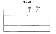
- FIG. 20 is a plan view illustrating a manufacturing step of a semiconductor laser diode, according to some other embodiments.
- FIG. 1 is a plan view for illustrating a configuration of a semiconductor laser diode according to some embodiments.
- FIG. 2 is a section view taken along line II-II in FIG. 1 .
- FIG. 3 is a section view taken along line III-III in FIG. 1 .
- the semiconductor laser diode 70 is a three-time-grown semiconductor laser diode manufactured through a three-time crystal growing step.
- the semiconductor laser diode 70 is also a Fabry-Perot type semiconductor laser diode including, as shown in FIGS.
- a substrate 1 a semiconductor laminate structure 2 formed on the substrate 1 by crystal growth, an n-type electrode 3 formed in contact with the rear surface of the substrate 1 (the opposite surface of the substrate 1 from the semiconductor laminate structure 2 ) and a p-type electrode 4 formed in contact with the front surface of the semiconductor laminate structure 2 .
- the substrate 1 may be formed of a GaAs monocrystalline substrate, but other types of substrates are possible.
- the plane direction of the front surface of the GaAs substrate 1 has an off-angle of 10 degrees with respect to a (100) plane.
- Individual layers that make up the semiconductor laminate structure 2 are caused to epitaxially grow with respect to the substrate 1 .
- the term “epitaxial growth” used herein refers to crystal growth performed while keeping the continuity of lattices from a ground layer. The mismatch of the lattices with respect to the ground layer is absorbed by the distortion of lattices of a crystal-grown layer, thereby maintaining the continuity of lattices on the interface with the ground layer.
- the semiconductor laminate structure 2 includes an active layer 10 , an n-side guide layer 11 , a p-side guide layer 12 , an n-type semiconductor layer 13 and a p-type semiconductor layer 14 .
- the n-type semiconductor layer 13 is arranged between the n-side guide layer 11 and the top surface of the substrate 1 .
- the n-side guide layer 11 is arranged between the n-type semiconductor layer 13 and the active layer 10 .
- the p-type semiconductor layer 14 is arranged on the p-side of the active layer 10 at which the p-type electrode 4 exists.
- the p-side guide layer 12 is arranged between the active layer 10 and the p-type semiconductor layer 14 .
- Electrons are implanted into the active layer 10 from the n-type semiconductor layer 13 via the n-side guide layer 11 .
- Positive holes are implanted into the active layer 10 from the p-type semiconductor layer 14 via the p-side guide layer 12 .
- Light is emitted as the electrons and the positive holes are recombined in the active layer 10 .
- the n-type semiconductor layer 13 is formed by laminating an n-type GaAs buffer layer 15 and an n-type (Al x1 Ga (1-x1) ) 0.51 In 0.49 P clad layer (0 ⁇ x1 ⁇ 1) 16 from the front side of the substrate 1 .
- the width of the n-type GaAs buffer layer 15 may be one of many possible widths.
- the thickness of the n-type GaAs buffer layer 15 may be 50 nm to 100 nm or may have a thickness of 100 nm.
- the n-type (Al x1 Ga (1-x1) ) 0.51 In 0.49 P clad layer (0 ⁇ x1 ⁇ 1) 16 may also be one of many possible widths, and may, for example, have a thickness of 2000 nm to 3000 nm or a thickness of 2500 nm.
- the p-type semiconductor layer 14 may be formed by laminating, on the p-type guide layer 12 , a first p-type (Al x1 Ga (1-x1) ) 0.51 In 0.49 P clad layer (0 ⁇ x1 ⁇ 1) 17 , a p-type InGaP etching stop layer 18 , a second p-type (Al x1 Ga (1-x1) ) 0.51 In 0.49 P clad layer (0 ⁇ x1 ⁇ 1) 19 , a p-type GaAs cap layer 20 and a p-type GaAs contact layer 21 .
- the first p-type (Al x1 Ga (1-x1) ) 0.51 In 0.49 P clad layer (0 ⁇ x1 ⁇ 1) 17 may have a thickness of, e.g., 250 nm to 400 nm or a thickness of 300 nm, but other widths may be possible.
- the p-type InGaP etching stop layer 18 may have a thickness of, e.g., 5 nm to 10 nm, or a thickness of 5 nm, but other widths may be possible.
- the second p-type (Al x1 Ga (1-x1) ) 0.51 In 0.49 P clad layer (0 ⁇ x1 ⁇ 1) 19 may have a thickness of, e.g., 1000 nm to 1500 nm, or a thickness of 1000 nm, but other widths are possible.
- the p-type GaAs cap layer 20 may have a thickness of, e.g., 50 nm to 100 nm, or a thickness of 100 nm but other widths are possible.
- the p-type GaAs contact layer 21 may have a thickness of, e.g., 1000 nm to 2000 nm, or a thickness of 1000 nm but other widths are possible.
- the n-type GaAs buffer layer 15 is provided to increase the adhesiveness between the GaAs substrate 1 and the n-type (Al x1 Ga (1-x1) ) 0.51 In 0.49 P clad layer 16 .
- the n-type GaAs buffer layer 15 may become an n-type semiconductor layer by doping, e.g., utilizing an Si as an n-type dopant, on GaAs.
- the p-type GaAs contact layer 21 is a low resistance layer for making ohmic contact with the p-type electrode 4 .
- the p-type GaAs contact layer 21 may become a p-type semiconductor layer by doping, e.g., utilizing Zn as a p-type dopant, on GaAs. It will be appreciated, however, that other dopants may be utilized.
- the n-type clad layer 16 and the first and second p-type clad layers 17 and 19 provide a carrier confinement effect by which the carriers (electrons and positive holes) are confined in the active layer 10 , and a light confinement effect by which the light coming from the active layer 10 is confined between the n-type clad layer 16 and the first and second p-type clad layers 17 and 19 .
- the n-type (Al x1 Ga (1-x1) ) 0.51 In 0.49 P clad layer 16 may be converted to an n-type semiconductor layer by doping, e.g., Si as an n-type dopant, on (Al x1 Ga (1-x1) ) 0.51 In 0.49 P.
- the first and second p-type (Al x1 Ga (1-x1) ) 0.51 In 0.49 P clad layers 17 and 19 are converted to p-type semiconductor layers by doping, e.g., Zn as a p-type dopant, on (Al x1 Ga (1-x1) ) 0.51 In 0.49
- the clad layers 16 , 17 and 19 may have a dopant concentration of not less than 0.7 ⁇ 10 18 cm ⁇ 3 and not greater than 2.0 ⁇ 10 18 cm ⁇ 3 . In some embodiments if the dopant concentration is lower than 0.7 ⁇ 10 18 cm ⁇ 3 , it sometimes becomes difficult to implant the carriers into the active layer 10 . In other alternate embodiments, if the dopant concentration is higher than 2.0 ⁇ 10 18 cm ⁇ 3 , the carriers are sometimes excessively implanted into the active layer 10 . The excess carriers become a light absorbing source, thereby worsening the oscillation efficiency.
- the n-type (Al x1 Ga (1-x1) ) 0.51 In 0.49 P clad layer 16 is wider in band gap than the n-side guide layer 11 .
- the first and second p-type (Al x1 Ga (1-x1) ) 0.51 In 0.49 P clad layers 17 and 19 are wider in band gap than the p-side guide layer 12 . This makes it possible to perform the carrier confinement and the light confinement in an efficient manner and to realize a highly efficient semiconductor laser diode.
- end surface window structures 40 for expanding the band gap of the active layer 10 may be formed by diffusing impurities such as zinc, or the like, into the laser resonator end surface portions.
- the diffusing velocity becomes faster if phosphorus is contained in the region to which impurities are to be diffused.
- each of the n-type clad layer 16 and the first and second p-type clad layers 17 and 19 is formed of a (Al x1 Ga (1-x1) ) 0.51 In 0.49 P layer containing phosphorus. Accordingly, it becomes easy to diffuse impurities such as zinc, or the like, which in turn makes it easy to form the end surface window structures 40 . This makes it possible to realize a semiconductor laser diode which is suitable for a large output.
- the n-type clad layer 16 and the first and second p-type clad layers 17 and 19 are lattice-matched with the GaAs substrate 1 because the composition ratio of Indium to (Al x1 Ga (1-x1) ) is set equal to 0.51:0.49. It is therefore possible to obtain high-quality crystals. As a result, it is possible to obtain a highly reliable semiconductor laser device.
- the n-side guide layer 11 is formed of a Al x2 Ga (1-x2) As (0 ⁇ x2 ⁇ 1) layer (having a thickness of, for example, 20 nm to 30 nm or a thickness of 20 nm) and is laminated on the n-type semiconductor layer 13 .
- the p-side guide layer 12 is formed of a Al x2 Ga (1-x2) As (0 ⁇ x2 ⁇ 1) layer (having a thickness of, for example, 20 nm to 30 nm or a thickness of 20 nm) and is laminated on the active layer 10 .
- the n-side Al x2 Ga (1-x2) As guide layer 11 and the p-side Al x2 Ga (1-x2) As guide layer 12 are semiconductor layers that cause a light confinement effect to occur in the active layer 10 . Additionally, in cooperation with the clad layers 16 , 17 and 19 , the n-side Al x2 Ga (1-x2) As guide layer 11 and the p-side Al x2 Ga (1-x2) As guide layer 12 form a carrier confinement structure for blocking carriers within the active layer 10 . This makes it possible to increase the efficiency of recombination of electrons and positive holes in the active layer 10 .
- the clad layers 16 , 17 and 19 are formed of (Al x1 Ga (1-x1) ) 0.51 In 0.49 P (0 ⁇ x1 ⁇ 1) while the guide layers 11 and 12 are formed of Al x2 Ga (1-x2) As (0 ⁇ x2 ⁇ 1). It is therefore possible to increase the band gap difference between the clad layers 16 , 17 and 19 and the guide layers 11 and 12 . It will be appreciated that other compositions may be utilized to achieve a comparable effect. Since the lattice constants of the clad layers 16 , 17 and 19 and that of the guide layers 11 and 12 differ from each other, it is possible to differentiate the diffusing velocity of carriers in the clad layers 16 , 17 and 19 and the diffusing velocity of carriers in the guide layers 11 and 12 .
- the (Al x1 Ga (1-x1) ) 0.51 In 0 49 P layer forming each of the clad layers 16 , 17 and 19 may have a composition, where, x1>0.7.
- the Al x2 Ga (1-x2) As layer forming each of the guide layers 11 and 12 may also have a composition, where 0.4 ⁇ x2 ⁇ 0.8.
- the reasons are as follows.
- the band gaps of the clad layers 16 , 17 and 19 and the guide layers 11 and 12 become greater as the Al composition grows higher.
- the band gap difference between the guide layers 11 and 12 and the clad layers 16 , 17 and 19 may be set equal to or greater than a predetermined value in order to prevent the carriers from being excessively implanted into the active layer 10 .
- the band gap difference can be made equal to or greater than the predetermined value by setting x1 greater than 0.7 and setting x2 equal to or smaller than 0.8.
- the band gap of the active layer 10 in the laser resonator end surface portions may become equal to the average value of the band gap of the resonator center portion and the band gap of the guide layers 11 and 12 .
- the band gap of the guide layers 11 and 12 may be configured to be equal to or greater than a predetermined value (e.g., about 1.8 eV).
- the band gap of the guide layers 11 and 12 can be made equal to or greater than the predetermined value by setting x2 equal to or greater than 0.4.
- the thickness of the first p-type clad layer 17 may be not less than 300 nm and not greater than 400 nm. In some embodiments, if the thickness of the first p-type clad layer 17 is smaller than 300 nm, it is sometimes difficult to reduce the refractive index difference between the first p-type clad layer 17 and the active layer 10 . Thus, a kink is generated with ease. In other alternate embodiments, if the thickness of the first p-type clad layer 17 is greater than 400 nm, the current flow path extending from the second p-type clad layer 19 to the active layer 10 may possibly become longer, thereby deteriorating the characteristics.
- the active layer 10 may have a multiple-quantum well-structure containing, for example, AlGaAsP.
- the active layer 10 may be a layer for amplifying a light generated by the recombination of electrons and positive holes.
- the active layer 10 has a multiple-quantum well-structure formed by alternately and repeatedly laminating, through a plurality of cycles, shown as quantum well layers 221 and barrier layers 222 each containing an undoped Al x2 Ga (1-x2) As layer (0 ⁇ x2 ⁇ 1).
- the quantum well layers 221 have a thickness of, for example, 9 nm to 12 nm or a thickness of 12 nm, but other widths are possible.
- the quantum well layers 221 also include an undoped GaAs (1-x3) P x3 layer (0 ⁇ x3 ⁇ 1).
- the barrier layers 222 include an undoped Al x2 Ga (1-x2) As layer (0 ⁇ x2 ⁇ 1).
- the thickness of the barrier layers 222 may be set greater than 4 nm but smaller than the thickness of the quantum well layers 221 . In some embodiments, the thickness of the barrier layers 222 is 6.5 nm. Similar to the guide layers 11 and 12 , the Al x2 Ga (1-x2) As layers forming the barrier layers 222 may have a composition, where 0.4 ⁇ x2 ⁇ 0.8.
- the lattice constant of the GaAsP layers in an unstrained state is smaller than the lattice constant of the GaAs substrate 1 , a tensile stress (or a tensile strain) is generated in each of the quantum well layers 221 containing the GaAs (1-x3) P x3 layer.
- This enables the semiconductor laser diode 70 to oscillate in a TM mode.
- the light outputted in the TM mode becomes a TM wave in which the magnetic field direction is perpendicular to the light propagation direction (namely, the electric field direction is parallel to the light propagation direction).
- a tensile strain having a lattice mismatch rate of not greater than ⁇ 0.4% and not less than ⁇ 0.9% may be generated in each of the quantum well layers 221 .
- the lattice mismatch rate is greater than ⁇ 0.4% (if the tensile strain is small)
- the oscillation in the TM mode is sometimes difficult to achieve.
- the lattice mismatch rate is smaller than ⁇ 0.9% (if the tensile strain is large) crystal defects may sometimes be generated with ease.
- the oscillation wavelength may be not less than 780 nm and not greater than 830 nm, and the thickness of the quantum well layers 221 may be not less than 9 nm and not greater than 12 nm. If the oscillation wavelength and the thickness of the quantum well layers 221 satisfy the above-noted conditions, it is sometimes possible to keep a TM component light output greater than a TE component light output and to reduce a threshold current.
- the GaAs (1-x3) P x3 layer forming the quantum well layers 221 may have a composition satisfying the conditions of the ratio x3/(1 ⁇ x3), where the composition x3 of P to the composition (1 ⁇ x3) of As is not less than 1/9 and not greater than 1/4.
- the reasons are as follows. In order to cause the semiconductor laser diode 70 to oscillate in the TM mode, a tensile strain may be generated in each of the quantum well layers 221 . If the lattice constant of the quantum well layers 221 grows smaller, it is possible to generate a greater tensile strain in each of the quantum well layers 221 .
- the lattice constant of the GaAs (1-x3) P x3 layer forming the quantum well layers 221 grows smaller as the ratio x3/(1 ⁇ x3) of the composition of P to the composition of As becomes greater. In other words, if the ratio x3/(1 ⁇ x3) becomes larger, it is possible to generate a greater tensile strain in each of the quantum well layers 221 .
- the reason for the ratio x3/(1 ⁇ x3) being not less than 1/9 is to increase the ratio of the TM component light output to the TE component light output.
- the reason for the ratio x3/(1 ⁇ x3) being not greater than 1/4 is that, if the ratio x3/(1 ⁇ x3) is greater than 1/4, the tensile strain generated in each of the quantum well layers 221 due to the increase of the P composition becomes greater, which may possibly generate a crack and a leak current.
- the number of the quantum well layers 221 may be not less than 2 and not greater than 5. If the number of the quantum well layers 221 is less than 2, the thickness of one of the quantum well layers 221 may be adjusted. Thus, crystal defects are generated with ease. On the other hand, if the number of the quantum well layers 221 is greater than 5, there exist an increased number of interfaces. Thus, crystal defects are generated with ease. As shown in FIG. 3 , a ridge stripe 30 may be formed by partially removing the second p-type clad layer 19 and the p-type cap layer 20 existing within the p-type semiconductor layer 14 .
- the second p-type clad layer 19 and the p-type cap layer 20 are partially etched away to form a ridge stripe 30 having a substantially trapezoidal shape (mesa shape) when seen in a cross section view.
- the ridge stripe 30 is formed of the second p-type clad layer 19 and the p-type cap layer 20 .
- the width of the surface of the second p-type clad layer 19 existing at the same side as the first p-type clad layer 17 (the first ridge width) will be referred to as “ridge bottom width W 1 ”.
- the width of the surface of the second p-type clad layer 19 existing at the opposite side from the first p-type clad layer 17 (the second ridge width) will be referred to as “ridge top width W 2 ”.
- the ridge bottom width W 1 is not less than 3.0 ⁇ m and not greater than 4.5 ⁇ m, and, more specifically, equal to 3.5 ⁇ m. If the ridge bottom width W 1 is less than 3.0 ⁇ m, carriers tend to concentrate on the width-wise central region of the semiconductor laser diode 70 during operation and the current density grows higher. Therefore, a kink is generated with ease. On the other hand, if the ridge bottom width W 1 is greater than 4.5 ⁇ m, a current diffusing range becomes greater and a carrier supply shortage occurs during operation. Therefore, a kink is generated with ease.
- the ridge bottom width W 1 is set not less than 3.0 ⁇ m and not greater than 4.5 ⁇ m, in some embodiments, it is possible to restrain or prevent generation of the kink. Accordingly, it is possible to obtain a semiconductor laser device with stable characteristics.
- the ridge top width W 2 is not less than 2.0 ⁇ m, and more specifically, equal to 2.5 ⁇ m. If the ridge top width W 2 is less than 2.0 ⁇ m, the resistance of the ridge stripe 30 becomes greater. The increase in the resistance of the ridge stripe 30 leads to an increase in an operating current and a decrease in a peak value of the light output. Since the ridge top width W 2 is set not less than 2.0 ⁇ m, it is possible to reduce the resistance of the ridge stripe 30 . This makes it possible to lower the operating current and to prevent the decrease in the peak value of the light output.
- n-type (Al x4 Ga (1-x4) ) 0.51 In 0.49 P (0 ⁇ x4 ⁇ 1) current-blocking layer (current-embedding layer) 6 which may have a thickness of 300 nm to 450 nm or a thickness of 400 nm, for example. More specifically, the side surfaces of the p-type cap layer 20 , the exposed surfaces of the second p-type clad layer 19 and the exposed surfaces of the p-type etching stop layer 18 are covered with the n-type AlGaInP current-blocking layer 6 in an intermediate region other than the opposite end regions near the opposite end surfaces 31 and 32 , as shown in FIG. 2 .
- the top and side surfaces of the p-type cap layer 20 , the exposed surfaces of the second p-type clad layer 19 and the exposed surfaces of the p-type etching stop layer 18 are covered with the n-type AlGaInP current-blocking layer 6 in the opposite end regions, as shown in FIGS. 2 and 3 .
- the n-type (Al x4 Ga (1-x4) ) 0 51 In 0.49 P current-blocking layer 6 becomes an n-type semiconductor layer by doping, e.g., utilizing Si as an n-type dopant, on (Al x4 Ga (1-x4) ) 0.51 In 0.49 P.
- the n-type (Al x4 Ga (1-x4) ) 0.51 In 0.49 P (0 ⁇ x4 ⁇ 1) layer forming the current-blocking layer 6 may have a composition, where 0.7 ⁇ x4 ⁇ 0.9. The reasons are as follows.
- the refractive index of the current-blocking layer 6 grows smaller. If x4 is smaller than 0.7, the refractive index difference between the first and second p-type clad layers 17 and 19 and the current-blocking layer 6 becomes smaller. This weakens the light confinement effect in the width direction provided by the current-blocking layer 6 . Thus, the operating current grows larger and the peak output becomes smaller.
- the n-type (Al 4 Ga (1-x4) ) 0.51 In 0.49 P layer forming the current-blocking layer 6 has a composition, where 0.7 ⁇ x4 ⁇ 0.9. It is therefore possible to prevent reduction of the peak output and to restrain or prevent generation of a kink. This makes it possible to obtain a semiconductor laser device which is suitable for high output and stable characteristics.
- the thickness of the current-blocking layer 6 may be not less than 300 nm and not greater than 450 nm. If the thickness of the current-blocking layer 6 is less than 300 nm, it is likely that, when seen in a cross section view, the light beam emits toward the contact layer 21 beyond the current-blocking layer 6 .
- the semiconductor laminate structure 2 may have a pair of end surfaces (cleavage surfaces) 31 and 32 formed of the longitudinal opposite cleavage surfaces of the ridge stripe 30 .
- the end surfaces 31 and 32 may be parallel to each other.
- the n-side guide layer 11 , the active layer 10 and the p-side guide layer 12 make up a Fabry-Perot resonator in which the end surfaces 31 and 32 are used as resonator end surfaces.
- the light generated in the active layer 10 is amplified by inductive emission while traveling between the resonator end surfaces 31 and 32 .
- the light thus amplified is partially emitted, as laser light, from the resonator end surfaces 31 and 32 to the outside of the semiconductor laser device.
- the n-type electrode 3 may be made of, for example, an AuGe/Ni/Ti/Au alloy, and may be ohmic-joined to the substrate 1 so that the AuGe side thereof can be positioned at the rear side of the substrate 1 .
- the p-type electrode 4 may be made of, for example, a Ti/Au alloy, and may be ohmic-joined to the p-type contact layer 21 so that the Ti side thereof can be positioned on the p-type contact layer 21 .
- the end surface window structures 40 for expanding the band gap of the active layer 10 may be formed in the end surface portions of the resonator.
- the end surface window structures 40 may be formed by, for example, diffusing zinc (Zn) into the resonator end surface portions.
- the diffusion length L of zinc from the interface between the n-side guide layer 11 and the n-type clad layer 16 toward the n-type clad layer 16 may be not less than 400 nm and not greater than 1300 nm. In some embodiments, if the diffusion length L is less than 400 nm, it sometimes becomes difficult to obtain the effect provided by the end surface window structures. In other alternate embodiments, if the diffusion length L is greater than 1300 nm, the diffusion amount of impurities (zinc in this case) sometimes becomes larger, which may possibly result in deterioration of characteristics.
- the n-type electrode 3 and the p-type electrode 4 are connected to a power source. Electrons and positive holes are implanted from the n type semiconductor layer 13 and the p-type semiconductor layer 14 into the active layer 10 , whereby the electrons and the positive holes are recombined within the active layer 10 .
- the light is amplified by inductive emission while repeating traveling between the resonator end surfaces 31 and 32 along the guide layers 11 and 12 . Then, a greater laser output is taken out from the resonator end surface 31 as a laser emitting surface.
- FIGS. 5 through 11 are horizontal section views showing a manufacturing method of the semiconductor laser diode 70 shown in FIGS. 1 through 3 .
- FIGS. 5, 7, 8 and 9 are horizontal section views of the central portion, which correspond to FIG. 3 .
- FIG. 6 is a horizontal section view of the portion near the opposite ends.
- FIGS. 10 and 11 are plan views.
- an n-type GaAs buffer layer 15 an n-type (Al x1 Ga (1-x1) ) 0.51 In 0.49 P clad layer 16 , an n-side Al x2 Ga (1-x2) As guide layer 11 , an active layer 10 , a p-side Al x2 Ga (1-x2) As guide layer 12 , a first p-type (Al x1 Ga (1-x1) ) 0.51 In 0.49 P clad layer 17 , a p-type InGaP etching stop layer 18 , a second p-type (Al x1 Ga (1-x1) ) 0.51 In 0.49 P clad layer 19 and a p-type GaAs cap layer 20 may be grown on a GaAs substrate 1 one after another by MOCVD (metal organic chemical vapor deposition) (a first crystal growth step).
- MOCVD metal organic chemical vapor deposition
- the active layer 10 is formed by causing quantum well layers 221 each including a GaAs (1-x3) P x3 layer and barrier layers 222 each including a Al x2 Ga (1-x2) As layer to alternately and repeatedly grow through a plurality of cycles.
- a ZnO (zinc oxide) layer 51 may be patterned on the p-type GaAs cap layer 20 in the regions near the end surfaces of the semiconductor laser diode 70 .
- Zn is diffused into the regions near the end surfaces of the semiconductor laser diode 70 by, for example, performing an annealing treatment for about two hours at a temperature of 500 to 600 degrees Celsius.
- the annealing treatment may be performed such that the diffusion length L of Zn from the interface between the n-side guide layer 11 and the n-type clad layer 16 toward the n-type clad layer 16 falls within a range of from 400 nm to 1300 nm.
- end surface window structures 40 can be formed in the regions near the end surfaces of the semiconductor laser diode 70 .
- the ZnO layer 51 may be removed.
- the p-type cap layer 20 and the second p-type clad layer 19 may be partially removed through an etching step in which a stripe-shaped SiO 2 insulation film is used as a mask layer 52 .
- a ridge stripe 30 having the mask layer 52 on the top surface thereof may be formed.
- only the portions 52 a (see FIG. 11 ) of the mask layer 52 existing in the regions near the end surfaces of the semiconductor laser diode 70 may be removed.
- an n-type (Al x4 Ga (1-x4) ) 0.51 In 0.49 P current-blocking layer 6 may be formed on the surface of the ridge stripe 30 (a second crystal growth step).
- the mask layer 52 serves as a mask.
- the top surface of the ridge stripe 30 (the upper surface of the p-type cap layer 20 ) may not covered with the n-type current-blocking layer 6 in the region corresponding to the intermediate portion between the opposite end portions of the semiconductor laser diode 70 .
- the top surface of the ridge stripe 30 (the upper surface of the p-type cap layer 20 ) may be covered with the n-type current-blocking layer 6 in the regions near the end surfaces of the semiconductor laser diode 70 .
- a p-type GaAs contact layer 21 may be grown on the surfaces of the n-type current-blocking layer 6 and the p-type cap layer 20 (a third crystal growth step). Finally, a p-type electrode 4 making ohmic contact with the p-type GaAs contact layer 21 may be formed and an n-type electrode 3 making ohmic contact with the GaAs substrate 1 may be formed.
- the polarization ratio may be determined utilizing any combination of parameters. For illustration purposes, the following four scenarios are provided:
- a: semiconductor laser device including an active layer 10 , the quantum well layers 221 having a thickness from 9 nm to 12 nm, and an oscillation wavelength from 820 nm to 830 nm;
- semiconductor laser device including an active layer 10 , the quantum well layers 221 having a thickness from 9 nm to 12 nm, and an oscillation wavelength from 800 nm to 820 nm;
- semiconductor laser device including an active layer 10 , the quantum well layers 221 having a thickness from 9 nm to 12 nm, and an oscillation wavelength from 790 nm to 800 nm;
- the tensile strain amount [%] of the active layers 10 for the sample scenarios are a ⁇ b ⁇ c ⁇ d. In other words, the tensile strain of sample a is smallest and the tensile strain of sample d is greatest.
- the conducting condition may be 60 mW at 25 degrees Celsius.
- the measurement results of polarization ratios [dB] with respect to samples a through d are shown in Table 1. When the tensile strain amount [%] of the quantum well layers 221 is zero, the polarization ratio [dB] is approximately ⁇ 35.
- the polarization ratios [dB] of all the samples are positive and further that the TM component light output is greater than the TE component light output in all the samples.
- the following section below describes the relationship between the tensile strain amount [%] of the active layer 10 and the threshold current [mA]. Using the same sample scenarios a through d above, and a conducting condition at 25 degrees Celsius, the measurements of threshold currents [mA] with respect to samples a through d are shown in Table 2. When the tensile strain amount [%] of the quantum well layers 221 is zero, the threshold current [mA] is approximately 24.5 mA.
- the threshold currents [mA] of all the samples are lower than the threshold current available when the tensile strain amount [%] is zero.
- FIG. 12 is a plan view for illustrating the configuration of a semiconductor laser diode according some embodiments.
- FIG. 13 is a section view taken along line XIII-XIII in FIG. 12 .
- FIG. 14 is a section view taken along line XIV-XIV in FIG. 12 .
- the portions corresponding to the respective portions shown in FIGS. 1 through 3 are designated by the same reference numerals as used in FIGS. 1 through 3 .
- the semiconductor laser diode 80 may be a one-time-grown semiconductor laser diode manufactured through a one-time crystal growth step.
- the semiconductor laser diode 80 is a Fabry-Perot type semiconductor laser diode including a substrate 1 , a semiconductor laminate structure 2 A formed on the substrate 1 by crystal growth, an n-type electrode 3 formed in contact with the rear surface of the substrate 1 (the opposite surface of the substrate 1 from the semiconductor laminate structure 2 A) and a p-type electrode 4 formed in contact with the front surface of the semiconductor laminate structure 2 A.
- the substrate 1 is formed of a GaAs monocrystalline substrate.
- the plane direction of the front surface of the GaAs substrate 1 has an off-angle of 10 degrees with respect to a (100) plane.
- Individual layers making up the semiconductor laminate structure 2 A are caused to epitaxially grow with respect to the substrate 1 .
- the semiconductor laminate structure 2 A includes an active layer 10 , an n-side guide layer 11 , a p-side guide layer 12 , an n-type semiconductor layer 13 and a p-type semiconductor layer 14 A.
- the n-type semiconductor layer 13 is arranged on the substrate 1 facing the active layer 10 .
- the p-type semiconductor layer 14 A is arranged between the active layer 10 and the p-type electrode 4 .
- the n-side guide layer 11 is arranged between the n-type semiconductor layer 13 and the active layer 10 .
- the p-side guide layer 12 is arranged between the active layer 10 and the p-type semiconductor layer 14 A. Thus, there is formed a double hetero-junction.
- Electrons are implanted into the active layer 10 from the n-type semiconductor layer 13 via the n-side guide layer 11 .
- Positive holes are implanted into the active layer 10 from the p-type semiconductor layer 14 A via the p-side guide layer 12 .
- Light is emitted as the electrons and the positive holes are recombined in the active layer 10 .
- the n-type semiconductor layer 13 is formed by laminating an n-type GaAs buffer layer 15 and an n-type (Al x1 Ga (1-x1) ) 0.51 In 0.49 P clad layer (0 ⁇ x1 ⁇ 1) 16 in the named order from the side of the substrate 1 .
- the n-type GaAs buffer layer 15 has a thickness of, for example, 50 nm to 100 nm or a thickness of 100 nm.
- the n-type (Al x1 Ga (1-x1) ) 0.51 In 0.49 P clad layer (0 ⁇ x1 ⁇ 1) 16 has a thickness of, for example, 2000 nm to 3000 nm or a thickness of 2500 nm.
- the p-type semiconductor layer 14 A may be formed by laminating, on the p-type guide layer 12 , a first p-type (Al x1 Ga (1-x1) ) 0.51 In 0.49 P clad layer (0 ⁇ x1 ⁇ 1) 17 , a p-type InGaP etching stop layer 18 , a second p-type (Al x1 Ga (1-x1) ) 0.51 In 0.49 P clad layer (0 ⁇ x1 ⁇ 1) 19 , and a p-type GaAs contact layer 21 A.
- the first p-type (Al x1 Ga (1-x1) ) 0.51 In 0.49 P clad layer (0 ⁇ x1 ⁇ 1) 17 has a thickness of, for example, 250 nm to 400 nm or a thickness of 350 nm.
- the p-type InGaP etching stop layer 18 has a thickness of, for example, 5 nm to 10 nm or a thickness of 5 nm.
- the second p-type (Al x1 Ga (1-x1) ) 0.51 In 0.49 P clad layer (0 ⁇ x1 ⁇ 1) 19 has a thickness of, for example, 1000 nm to 1500 nm or a thickness of 1000 nm.
- the p-type GaAs contact layer 21 A has a thickness of, for example, 100 nm to 300 nm or a thickness of 300 nm.
- the n-side guide layer 11 may be formed of a Al x2 Ga (1-x2) As (0 ⁇ x2 ⁇ 1) layer (having a thickness of, e.g., 20 nm to 30 nm, or a thickness of 20 nm) and is laminated on the n-type semiconductor layer 13 .
- the p-side guide layer 12 is formed of a Al x2 Ga (1-x2) As (0 ⁇ x2 ⁇ 1) layer (having a thickness of, e.g., 20 nm to 30 nm, or a thickness of 20 nm) and is laminated on the active layer 10 .
- the (Al x1 Ga (1-x1) ) 0.51 In 0.49 P layer forming each of the clad layers 16 , 17 and 19 may have a composition, where x1>0.7.
- the reasons are as follows.
- the band gaps of the clad layers 16 , 17 and 19 may become greater as the Al composition grows higher.
- the band gap difference between the guide layers 11 and 12 and the clad layers 16 , 17 and 19 may be set equal to or greater than a predetermined value in order for the clad layers 16 , 17 and 19 to satisfactorily perform carrier blocking and light confinement.
- the band gap difference can be made equal to or greater than the predetermined value by setting x1 greater than 0.7.
- the thickness of the first p-type clad layer 17 may be not less than 300 nm and not greater than 400 nm not to generate a kink easily. If the thickness of the first p-type clad layer 17 is smaller than 300 nm, it is impossible to reduce the refractive index difference between the first p-type clad layer 17 and the active layer 10 . On the other hand, if the thickness of the first p-type clad layer 17 is greater than 400 nm, the current flow path extending from the second p-type clad layer 19 to the active layer 10 becomes longer, thereby deteriorating the characteristics.
- the active layer 10 has a multiple-quantum well structure containing, e.g., AlGaAsP.
- the active layer 10 has a multiple-quantum well structure formed by alternately and repeatedly laminating, through a plurality of cycles, quantum well layers 221 and barrier layers 222 .
- the quantum well layers 221 have a thickness of, for example, 8 nm to 14 nm or a thickness of 13 nm, and may include undoped GaAs (1-x3) P x3 layers (0 ⁇ x3 ⁇ 1).
- the barrier layers 222 may include undoped Al x2 Ga (1-x2) As layers (0 ⁇ x2 ⁇ 1).
- the thickness of the barrier layers 222 may be set greater than 4 nm but smaller than the thickness of the quantum well layers 221 . In some embodiments, the thickness of the barrier layers 222 is 6.5 nm.
- the lattice constant of the GaAsP layers in an unstrained state is smaller than the lattice constant of the GaAs substrate 1 , a tensile stress (or a tensile strain) is generated in each of the quantum well layers 221 including the GaAs (1-x3) P x3 layer.
- This enables the semiconductor laser diode 80 to oscillate in a TM mode.
- the light outputted in the TM mode becomes a TM wave in which the magnetic field direction is perpendicular to the light propagation direction. Namely, the electric field direction is parallel to the light propagation direction.
- a ridge stripe 30 A is formed by partially removing the second p-type clad layer 19 and the p-type contact layer 21 A existing within the p-type semiconductor layer 14 A. More specifically, the second p-type clad layer 19 and the p-type contact layer 21 A may be partially etched away to form a ridge stripe 30 A having a substantially trapezoidal shape (mesa shape) when seen in a cross section view. In other words, the ridge stripe 30 A may be formed of the second p-type clad layer 19 and the p-type contact layer 21 A.
- the width of the surface of the second p-type clad layer 19 existing at the same side as the first p-type clad layer 17 (the first ridge width) will be referred to as “ridge bottom width W 1 ”.
- the width of the surface of the second p-type clad layer 19 existing at the opposite side from the first p-type clad layer 17 (the second ridge width) will be referred to as “ridge top width W 2 ”.
- the ridge bottom width W 1 is not less than 3.0 ⁇ m and not greater than 4.5 ⁇ m, and more specifically, equal to 3.5 ⁇ m. If the ridge bottom width W 1 is less than 3.0 ⁇ m, carriers tend to concentrate on the width-wise central region of the semiconductor laser diode 80 during operation and the current density grows higher. The increase in the current density causes sudden current implantation, which may possibly generate a kink. On the other hand, if the ridge bottom width W 1 is greater than 4.5 ⁇ m, a current diffusing range becomes greater during operation. The increase in the current diffusing range leads to carrier shortage, which may possibly generate a kink.
- the ridge bottom width W 1 is set not less than 3.0 ⁇ m and not greater than 4.5 ⁇ m, in some embodiments, it is possible to restrain or prevent generation of the kink. Accordingly, it is possible to obtain a semiconductor laser device with stable characteristics.
- the ridge top width W 2 is not less than 2.0 ⁇ m, and more specifically, equal to 2.5 ⁇ m. If the ridge top width W 2 is less than 2.0 ⁇ m, the resistance of the ridge stripe 30 A becomes greater. The increase in the resistance of the ridge stripe 30 A leads to an increase in an operating current and a decrease in a peak value of the light output. Since the ridge top width W 2 is set not less than 2.0 ⁇ m, in some embodiments, it is possible to reduce the resistance of the ridge stripe 30 A. This makes it possible to lower the operating current and to prevent the decrease in the peak value of the light output.
- a current-blocking layer (embedding layer) 6 A which has a thickness of, e.g., 200 nm to 300 nm, or a thickness of 250 nm and contains a SiO 2 or SiN insulation layer. More specifically, the side surfaces of the p-type contact layer 21 A, the exposed surfaces of the second p-type clad layer 19 and the exposed surfaces of the p-type etching stop layer 18 may be covered with the current-blocking layer 6 A.
- the thickness of the current-blocking layer 6 A may be not less than 200 nm and not greater than 300 nm. If the thickness of the current-blocking layer 6 A is less than 200 nm, it is likely that, when seen in a cross section view, the light beam emits from the current-blocking layer 6 A. On the other hand, if the thickness of the current-blocking layer 6 A is greater than 300 nm, a stress is generated in the active layer 10 due to the difference in thermal expansion coefficient between the current-blocking layer 6 A and the active layer 10 . This is because the SiO 2 or SiN insulation layer is hard. Consequently, it is likely that the magnitude of the tensile strain generated in the active layer 10 may undergo a change.
- the semiconductor laminate structure 2 A has a pair of end surfaces (cleavage surfaces) 31 and 32 formed of the longitudinal opposite cleavage surfaces of the ridge stripe 30 A.
- the end surfaces 31 and 32 are parallel to each other.
- the n-side guide layer 11 , the active layer 10 and the p-side guide layer 12 make up a Fabry-Perot resonator in which the end surfaces 31 and 32 are used as resonator end surfaces.
- the light generated in the active layer 10 is amplified by inductive emission while repeating traveling between the resonator end surfaces 31 and 32 .
- the light thus amplified is partially emitted, as laser light, from the resonator end surfaces 31 and 32 to the outside of the semiconductor laser device.
- the n-type electrode 3 may be made of, e.g., an AuGe/Ni/Ti/Au alloy, and is ohmic-joined to the substrate 1 so that the AuGe side thereof can be positioned at the rear side of the substrate 1 .
- the p-type electrode 4 may be made of, e.g., a Ti/Au alloy, and is ohmic-joined to the p-type contact layer 21 A so that the Ti side thereof can be positioned on the p-type contact layer 21 A. Again, other substitute materials may be possible. As shown in FIGS.
- the end surface window structures 40 for expanding the band gap of the active layer 10 may be formed in the end surface portions of the resonator.
- the end surface window structures 40 may be formed by, e.g., diffusing zinc (Zn) into the resonator end surface portions.
- the n-type electrode 3 and the p-type electrode 4 are connected to a power source. Electrons and positive holes are implanted from the n type semiconductor layer 13 and the p-type semiconductor layer 14 A into the active layer 10 , whereby the electrons and the positive holes are recombined within the active layer 10 .
- the light is amplified by inductive emission while repeating traveling between the resonator end surfaces 31 and 32 along the guide layers 11 and 12 . Then, a greater laser output is taken out from the resonator end surface 31 as a laser emitting surface.
- FIGS. 15 through 20 are horizontal section views showing a manufacturing method of the semiconductor laser diode 80 shown in FIGS. 12 through 14 , according to some embodiments.
- FIGS. 15, 17 and 18 are horizontal section views of the central portion, which correspond to FIG. 4 .
- FIG. 16 is a horizontal section view of the portion near the opposite ends.
- FIGS. 19 and 20 are plan views. First, as shown in FIG.
- an n-type GaAs buffer layer 15 an n-type (Al x1 Ga (1-x1) ) 0.51 In 0.49 P clad layer 16 , an n-side Al x2 Ga (1-x2) As guide layer 11 , an active layer 10 , a p-side Al x2 Ga (1-x2) As guide layer 12 , a first p-type (Al x1 Ga (1-x1) ) 0.51 In 0.49 P clad layer 17 , a p-type InGaP etching stop layer 18 , a second p-type (Al x1 Ga (1-x1) ) 0.51 In 0.49 P clad layer 19 and a p-type GaAs contact layer 21 A may be grown on a GaAs substrate 1 one after another by metal organic chemical vapor deposition.
- the active layer 10 may be formed by causing quantum well layers 221 each including a GaAs (1-x3) P x3 layer and barrier layers 222 each including a Al x2 Ga (1-x2) As layer to alternately and repeatedly grow through a plurality of cycles.
- a ZnO (zinc oxide) layer 51 may be patterned on the p-type GaAs contact layer 21 A in the regions near the ends of the semiconductor laser diode 80 . Then, Zn is diffused into the regions near the end surfaces of the semiconductor laser diode 80 by, e.g., performing an annealing treatment for about two hours at a temperature of 500 to 600 degrees Celsius. Thus, end surface window structures 40 may be formed in the regions near the end surfaces of the semiconductor laser diode 80 .
- the ZnO layer 51 is removed. Subsequently in some embodiments, as shown in FIGS. 17 and 20 , the p-type contact layer 21 A and the second p-type clad layer 19 are partially removed through an etching step in which a stripe-shaped SiO 2 insulation film is used as a mask layer 52 . Thus, a ridge stripe 30 A having the mask layer 52 on the top surface thereof may be formed. Thereafter, the mask layer 52 is removed. Next, an n-type current-blocking layer 6 A containing a SiO 2 or SiN insulation layer is formed on the surface of the ridge stripe 30 A. Thereafter, the current-blocking layer 6 A on the p-type contact layer 21 A is removed. Thus, as shown in FIG.
- the side surfaces of the ridge stripe 30 A are covered with the current-blocking layer 6 A but the top surface of the ridge stripe 30 A (the upper surface of the p-type contact layer 21 A) may not be covered with the current-blocking layer 6 A.
- a p-type electrode 4 making ohmic contact with the p-type GaAs contact layer 21 A may be formed and an n-type electrode 3 making ohmic contact with the GaAs substrate 1 may be formed.
Abstract
A semiconductor laser device includes an n-type clad layer, a first p-type clad layer and a ridge stripe. The device also includes an active layer interposed between the n-type clad layer and the first p-type clad layer, and a current-blocking layer formed on side surfaces of the ridge stripe. The ridge stripe of the device includes a second p-type clad layer formed into a ridge stripe shape on the opposite surface of the first p-type clad layer from the n-type clad layer. The ridge stripe is formed such that a first ridge width as the width of a surface of the second p-type clad layer exists on the same side as the first p-type clad layer and a second ridge width as the width of a surface of the second p-type clad layer exists on the opposite side from the first p-type clad layer.
Description
This application is a continuation of U.S. application Ser. No. 14/558,797, filed on Dec. 3, 2014, and allowed on Jul. 22, 2015, which is a Continuation of U.S. application Ser. No. 14/108,165, filed on Dec. 16, 2013 (now U.S. Pat. No. 8,923,355, issued on Dec. 30, 2014), which is a Continuation of U.S. application Ser. No. 13/359,494, filed on Jan. 26, 2012 (now U.S. Pat. No. 8,611,386, issued on Dec. 17, 1013). Further, the parent application Ser. No. 13/359,494 is based upon and claims the priority benefit of Japanese Patent Application Nos. 2011-15731 and 2011-15732, each filed on Jan. 27, 2011. The disclosures of these prior U.S. and Japanese applications are incorporated herein by reference.
The present disclosure(s) relate to a semiconductor laser device and a manufacturing method thereof.
In order to increase a storage capacity of a hard disc drive (HDD), there is a need to record signals in a microscale region of a disc. For the purpose of writing signals in the microscale region of a disc while assuring the stability of the recorded signals in the presence of thermal changes, it is necessary to use a thermally stable recording medium. This however poses a dilemma in that strong magnetic fields are required to rewrite the signals. Nowadays, the recording density grows saturated in an up-to-date GMR (Giant Magneto Resistance) method. Thus, there is a need for a “heat-assisted recording” method.
The present disclosure(s) include some embodiments of a semiconductor laser device capable of obtaining TM-mode oscillation. Moreover, the present disclosure(s) include some embodiments of a semiconductor laser device which is suitable for large output purposes and capable of obtaining stable TM-mode oscillation.
The “heat-assisted recording” method refers to a method in which, using a laser diode (semiconductor laser device) as a heat source, a force for holding magnetic fields is temporarily weakened and a writing task is performed in that state. Unlike a conventional semiconductor laser device for optical pickup, a semiconductor laser device used in a recording device of “heat-assisted recording” types need to generate a large output despite its small chip size. Since a restriction is imposed on the mounting space of the semiconductor laser device, it is sometimes necessary to realize not only TE (Transverse Electric) polarization, but also TM (Transverse Magnetic) polarization.
According to some embodiments, there is provided a semiconductor laser device. The semiconductor laser device includes a p-type clad layer and an n-type clad layer, a p-side guide layer and an n-side guide layer, and an active layer. The p-side guide layer and the n-side guide layer are interposed between the p-type clad layer and the n-type clad layer. The active layer is interposed between the p-side guide layer and the n-side guide layer. The active layer includes at least two quantum well layers and a barrier layer interposed between the quantum well layers adjoining to each other. Each of the p-type clad layer and the n-type clad layer is formed of a (Alx1Ga(1-x1))0.51In0.49P layer (0≦x1≦1). Each of the p-side guide layer, the n-side guide layer and the barrier layer is formed of an Alx2Ga(1-x2)As layer (0≦x2≦1). Each of the quantum well layers is formed of a GaAs(1-x3)Px3 layer (0≦x3≦1). The (Alx1Ga(1-x1))0.51In0.49P layer has a composition, where x1>0.7, and the Alx2Ga(1-x2)As layer having a composition, where 0.4≦x2≦0.8.
In the configuration of some embodiments, each of the p-type clad layer and the n-type clad layer is formed of a (Alx1Ga(1-x1))0.51In0.49P layer (0≦x1≦1) while each of the p-side guide layer and the n-side guide layer is formed of a Alx2Ga(1-x2)As layer (0≦x2≦1). It is therefore possible to increase the band gap difference between the clad layers and the guide layers. Since the clad layers and the guide layers are formed of materials differing in self-diffusing coefficient from each other, it is possible to make different the diffusing velocity of carriers in the clad layers and the diffusing velocity of carriers in the guide layers. This makes it possible to prevent the carriers from being excessively implanted into the active layer. As a consequence, it is possible to restrain or prevent occurrence of a so-called carrier overflow phenomenon in which the carriers overflow from the active layer to the clad layers or other surrounding layers in proportion to the rise in temperature. Accordingly, it is possible to restrain or prevent deterioration of characteristics which may be caused by the carrier overflow phenomenon.
In the configuration of some embodiments, the (Alx1Ga(1-x1))0.51In0.49 P layer has a composition, where x1>0.7, and the Alx2Ga(1-x2)As layer has a composition, where 0.4≦x2≦0.8. The reasons are as follows. The band gaps of the clad layers and the guide layers become greater as the Al composition grows higher. As set forth above, the band gap difference between the guide layers and the clad layers may be set equal to or greater than a predetermined value to prevent the carriers from being excessively implanted into the active layer. More specifically, the band gap of the clad layers may be increased, while the band gap of the guide layers is decreased. The band gap difference can be made equal to or greater than the predetermined value by setting x1 greater than 0.7 and setting x2 equal to or smaller than 0.8.
In the semiconductor laser device, a tensile strain may have a lattice mismatch rate of not greater than −0.4% and not less than −0.9% be generated in each of the quantum well layers. If the lattice mismatch rate is greater than −0.4% (if the tensile strain is too small), the oscillation in the TM mode is hard to occur. If the lattice mismatch rate is smaller than −0.9% (if the tensile strain is too large), crystal defects are generated with ease.
In the semiconductor laser device, the oscillation wavelength may be not less than 780 nm and not greater than 830 nm and that the thickness of each of the quantum well layers be not less than 9 nm and not greater than 12 nm. If the oscillation wavelength and the thickness of the quantum well layers satisfy the above-noted conditions, it is possible to keep a TM component light output greater than a TE component light output and to reduce a threshold current.
In the semiconductor laser device, the GaAs(1-x3)Px3 layer may have a composition satisfying a condition that a ratio x3/(1−x3) of a composition x3 of P to a composition (1−x3) of As is not less than 1/9 and not greater than 1/4. The reasons are as follows. In order to cause the semiconductor laser device to oscillate in the TM mode, it is necessary that a tensile strain is generated in each of the quantum well layers. If the lattice constant of the quantum well layers grows smaller, it is possible to generate a greater tensile strain in each of the quantum well layers. The lattice constant of the GaAs(1-x3)Px3 layer forming the quantum well layers grows smaller as the ratio x3/(1−x3) of the composition of P to the composition of As becomes greater. In other words, if the ratio x3/(1−x3) becomes larger, it is possible to generate a greater tensile strain in each of the quantum well layers.
The reason for the ratio x3/(1−x3) may be not less than 1/9 is to make the TM component light output greater than the TE component light output. On the other hand, the reason for the ratio x3/(1−x3) may be not greater than 1/4 is that, if the ratio x3/(1−x3) is greater than 1/4, the tensile strain generated in each of the quantum well layers due to the increase of the P composition becomes greater, which may possibly generate a crack and a leak current.
According to some embodiments, each of the quantum well layers has a thickness of not less than 9 nm and not greater than 12 nm, the barrier layer having a thickness smaller than the thickness of each of the quantum well layers. In the semiconductor laser device, the number of the quantum well layers may be not less than 2 and not greater than 5. If the number of the quantum well layers is less than 2, there is a need to increase the thickness of one of the quantum well layers. Thus, crystal defects are generated with ease. On the other hand, if the number of the quantum well layers is greater than 5, there exist an increased number of interfaces. Thus, crystal defects are generated with ease. In the semiconductor laser device, the p-type clad layer and the n-type clad layer may have a carrier concentration of not less than 0.7×1018 cm−3 and not greater than 2.0×1018 cm−3. If the carrier concentration is less than 0.7×1018 cm−3, it becomes difficult to implant the carriers into the active layer. On the other hand, if the dopant concentration is greater than 2.0×1018 cm−3, the carriers are excessively implanted into the active layer. The excess carriers become a light absorbing source, thereby worsening the oscillation efficiency.
In the semiconductor laser device, the end surface window structures for expanding a band gap of the active layer may be formed in end surface portions of a laser resonator. If the end surface window structures are formed in the end surface portions of the laser resonator, it is possible to expand the band gap of the active layer in the end surface portions. Thus, the inductively emitted light generated by the recombination of electrons and positive holes within the active layer is hard to be absorbed in the end surface portions of the laser resonator, which makes it possible to restrain generation of heat. It is therefore possible to reduce the end-surface optical damage and to acquire a large output.
In the semiconductor laser device, the end surface window structures may be formed by selectively diffusing impurities into the end surface portions of the laser resonator and that a diffusion length of the impurities from an interface between the n-side guide layer and the n-type clad layer toward the n-type clad layer is not less than 400 nm and not greater than 1300 nm. In some embodiments, when the diffusion length is less than 400 nm, it sometimes becomes difficult to obtain the effect provided by the end surface window structures. In other alternate embodiments, if the diffusion length is greater than 1300 nm, the diffusion amount of impurities sometimes becomes larger, which may possibly result in deterioration of the characteristics.
The semiconductor laser device, in some embodiments, includes: an n-type clad layer; a first p-type clad layer; a ridge stripe including a second p-type clad layer formed into a ridge stripe shape on the opposite surface of the first p-type clad layer from the n-type clad layer; an active layer interposed between the n-type clad layer and the first p-type clad layer such that a tensile strain is generated in the active layer; and a current-confining layer formed on the side surfaces of the ridge stripe. The ridge stripe is formed such that a first ridge width as the width of a surface of the second p-type clad layer existing at the same side as the first p-type clad layer is not less than 3.0 μm and not greater than 4.5 μm and a second ridge width as the width of a surface of the second p-type clad layer existing at the opposite side from the first p-type clad layer is not less than 2.0 μm. With this configuration, there is provided the active layer in which a tensile strain is generated. It is therefore possible to obtain a semiconductor laser device oscillating in the TM mode.
If the first ridge width is too small, carriers tend to concentrate on the width-wise central region of the semiconductor laser device during operation and the current density grows higher. Therefore, a kink is generated with ease. On the other hand, if the first ridge width is too large, a current diffusing range becomes greater and a carrier supply shortage occurs during operation. Therefore, a kink is generated with ease. Since the first ridge width is set not less than 3.0 μm and not greater than 4.5 μm, in some embodiments, it is possible to restrain or prevent generation of the kink. Accordingly, it is possible to obtain a semiconductor laser device with stable characteristics.
If the second ridge width is too small, the resistance of the ridge stripe becomes greater. The increase in the resistance of the ridge stripe leads to an increase in an operating current and a decrease in a peak value of the light output. Since the second ridge width is set not less than 2.0 μm, in some embodiments, it is possible to reduce the resistance of the ridge stripe. This makes it possible to lower the operating current and to prevent the decrease in the peak value of the light output.
In the semiconductor laser device, the first p-type clad layer may have a thickness of not less than 300 nm and not greater than 400 nm. If the thickness of the first p-type clad layer is smaller than 300 nm, it is difficult to reduce the refractive index difference between the first p-type clad layer and the active layer. Thus, a kink is generated with ease. On the other hand, if the thickness of the first p-type clad layer is greater than 400 nm, the current flow path extending from the second p-type clad layer to the active layer becomes longer, thereby deteriorating the characteristics.
In some embodiments, the semiconductor laser device is a three-time-grown semiconductor laser device manufactured by forming a p-type contact layer after the current-blocking layer is formed. The current-blocking layer is formed of an n-type (Alx4Ga(1-x4))0.51In0.49P (0≦x4≦1) layer that has a composition, where 0.7≦x4≦0.9.
If the Al composition in the n-type (Alx4Ga(1-x4))0.51In0.49P layer forming the current-blocking layer becomes greater, the refractive index of the current-blocking layer grows smaller. If x4 is smaller than 0.7, the refractive index difference between the first and second p-type clad layers and the current-blocking layer becomes smaller. This weakens the light confinement effect in the width direction provided by the current-blocking layer. Thus, the operating current grows larger and the peak output becomes smaller. On the other hand, if x4 is greater than 0.9, the refractive index difference between the first and second p-type clad layers and the current-blocking layer becomes too great. This makes too strong the light confinement effect in the width direction provided by the current-blocking layer. Thus, the light density is increased and the kink is generated with ease. In the embodiment set forth above, the (Alx4Ga(1-x4))0.51In0.49P layer has a composition, where 0.7≦x4≦0.9. It is therefore possible to prevent reduction of the peak output and to restrain or prevent generation of the kink. This makes it possible to obtain a semiconductor laser device which is suitable for large output purposes and stable in characteristics.
In the semiconductor laser device, the n-type (Alx4Ga(1-x4))0.51In0.49P current-blocking layer may have a thickness of not less than 300 nm and not greater than 450 nm. If the thickness of the current-blocking layer is less than 300 nm, it is likely that, when seen in a cross section view, the light beam emits toward the contact layer beyond the current-blocking layer. On the other hand, if the thickness of the current-blocking layer is greater than 450 nm, it becomes difficult to form the current-blocking layer.
According to some embodiments, the semiconductor laser device is a one-time-grown semiconductor laser manufactured by forming a p-type contact layer, when forming the second p-type clad layer, and then forming the current-blocking layer. The current-blocking layer is formed of a SiO2 layer or a SiN layer. In the semiconductor laser device, the current-blocking layer may have a thickness of not less than 200 nm and not greater than 300 nm. If the thickness of the current-blocking layer is less than 200 nm, it is likely that, when seen in a cross section view, the light beam emits from the current-blocking layer. On the other hand, if the thickness of the current-blocking layer is greater than 300 nm, a stress is generated in the active layer due to the difference in thermal expansion coefficient between the current-blocking layer and the active layer. This is because the SiO2 or SiN layer is hard. Consequently, it is likely that the magnitude of the tensile strain generated in the active layer may undergo a change.
In the semiconductor laser device, the end surface window structures for expanding a band gap of the active layer may be formed in end surface portions of a laser resonator. If the end surface window structures are formed in the end surface portions of the laser resonator, it is possible to expand the band gap of the active layer in the end surface portions. Thus, the inductively emitted light generated by the recombination of electrons and positive holes within the active layer is hard to be absorbed in the end surface portions of the laser resonator, which makes it possible to restrain generation of heat. It is therefore possible to reduce the end-surface optical damage and to acquire a large output of the device.
In the semiconductor laser device, the n-type clad layer, the first p-type clad layer and the second p-type clad layer may be formed of a (Alx1Ga(1-x1))0.51In0.49P layer that has a composition, where x1>0.7. The reasons are as follows. The band gaps of the n-type clad layer, the first p-type clad layer and the second p-type clad layer become greater as the Al composition grows higher. The band gap difference between the guide layers and the clad layers be set equal to or greater than a predetermined value in order for the clad layers to satisfactorily perform carrier confinement and light confinement. The band gap difference can be made equal to or greater than the predetermined value by setting x1 greater than 0.7.
According to some embodiments, there is provided a method of manufacturing a semiconductor laser device. The method includes forming an n-type clad layer; forming a first p-type clad layer; forming a ridge stripe including a second p-type clad layer formed into a ridge stripe shape on the opposite surface of the first p-type clad layer from the n-type clad layer; forming an active layer interposed between the n-type clad layer and the first p-type clad layer; and forming a current-blocking layer on side surfaces of the ridge stripe. The ridge stripe is formed is configured such that a first ridge width as the width of a surface of the second p-type clad layer exists on the same side as the first p-type clad layer and a second ridge width as the width of a surface of the second p-type clad layer exists at the opposite side from the first p-type clad layer.
Reference will now be made in detail to various embodiments, examples of which are illustrated in the accompanying drawings. In the following detailed description, numerous specific details are set forth in order to provide a thorough understanding of the present invention(s). However, it will be apparent to one of ordinary skill in the art that the present invention(s) may be practiced without these specific details. In other instances, well-known methods, procedures, systems, and components have not been described in detail so as not to unnecessarily obscure aspects of the various embodiments.
Various embodiments will now be described in detail with reference to the accompanying drawings. FIG. 1 is a plan view for illustrating a configuration of a semiconductor laser diode according to some embodiments. FIG. 2 is a section view taken along line II-II in FIG. 1 . FIG. 3 is a section view taken along line III-III in FIG. 1 . The semiconductor laser diode 70 is a three-time-grown semiconductor laser diode manufactured through a three-time crystal growing step. The semiconductor laser diode 70 is also a Fabry-Perot type semiconductor laser diode including, as shown in FIGS. 2 and 3 , a substrate 1, a semiconductor laminate structure 2 formed on the substrate 1 by crystal growth, an n-type electrode 3 formed in contact with the rear surface of the substrate 1 (the opposite surface of the substrate 1 from the semiconductor laminate structure 2) and a p-type electrode 4 formed in contact with the front surface of the semiconductor laminate structure 2.
The substrate 1 may be formed of a GaAs monocrystalline substrate, but other types of substrates are possible. The plane direction of the front surface of the GaAs substrate 1 has an off-angle of 10 degrees with respect to a (100) plane. Individual layers that make up the semiconductor laminate structure 2 are caused to epitaxially grow with respect to the substrate 1. The term “epitaxial growth” used herein refers to crystal growth performed while keeping the continuity of lattices from a ground layer. The mismatch of the lattices with respect to the ground layer is absorbed by the distortion of lattices of a crystal-grown layer, thereby maintaining the continuity of lattices on the interface with the ground layer.
The semiconductor laminate structure 2 includes an active layer 10, an n-side guide layer 11, a p-side guide layer 12, an n-type semiconductor layer 13 and a p-type semiconductor layer 14. The n-type semiconductor layer 13 is arranged between the n-side guide layer 11 and the top surface of the substrate 1. The n-side guide layer 11 is arranged between the n-type semiconductor layer 13 and the active layer 10.
The p-type semiconductor layer 14 is arranged on the p-side of the active layer 10 at which the p-type electrode 4 exists. The p-side guide layer 12 is arranged between the active layer 10 and the p-type semiconductor layer 14. Thus, there is formed a double hetero-junction. Electrons are implanted into the active layer 10 from the n-type semiconductor layer 13 via the n-side guide layer 11. Positive holes are implanted into the active layer 10 from the p-type semiconductor layer 14 via the p-side guide layer 12. Light is emitted as the electrons and the positive holes are recombined in the active layer 10.
The n-type semiconductor layer 13 is formed by laminating an n-type GaAs buffer layer 15 and an n-type (Alx1Ga(1-x1))0.51In0.49P clad layer (0≦x1≦1) 16 from the front side of the substrate 1. The width of the n-type GaAs buffer layer 15 may be one of many possible widths. For example, the thickness of the n-type GaAs buffer layer 15 may be 50 nm to 100 nm or may have a thickness of 100 nm. The n-type (Alx1Ga(1-x1))0.51In0.49P clad layer (0≦x1≦1) 16 may also be one of many possible widths, and may, for example, have a thickness of 2000 nm to 3000 nm or a thickness of 2500 nm.
The p-type semiconductor layer 14 may be formed by laminating, on the p-type guide layer 12, a first p-type (Alx1Ga(1-x1))0.51In0.49P clad layer (0≦x1≦1) 17, a p-type InGaP etching stop layer 18, a second p-type (Alx1Ga(1-x1))0.51In0.49P clad layer (0≦x1≦1) 19, a p-type GaAs cap layer 20 and a p-type GaAs contact layer 21. The first p-type (Alx1Ga(1-x1))0.51In0.49P clad layer (0≦x1≦1) 17 may have a thickness of, e.g., 250 nm to 400 nm or a thickness of 300 nm, but other widths may be possible. The p-type InGaP etching stop layer 18 may have a thickness of, e.g., 5 nm to 10 nm, or a thickness of 5 nm, but other widths may be possible. The second p-type (Alx1Ga(1-x1))0.51In0.49P clad layer (0≦x1≦1) 19 may have a thickness of, e.g., 1000 nm to 1500 nm, or a thickness of 1000 nm, but other widths are possible. The p-type GaAs cap layer 20 may have a thickness of, e.g., 50 nm to 100 nm, or a thickness of 100 nm but other widths are possible. The p-type GaAs contact layer 21 may have a thickness of, e.g., 1000 nm to 2000 nm, or a thickness of 1000 nm but other widths are possible.
The n-type GaAs buffer layer 15 is provided to increase the adhesiveness between the GaAs substrate 1 and the n-type (Alx1Ga(1-x1))0.51In0.49P clad layer 16. The n-type GaAs buffer layer 15 may become an n-type semiconductor layer by doping, e.g., utilizing an Si as an n-type dopant, on GaAs. The p-type GaAs contact layer 21 is a low resistance layer for making ohmic contact with the p-type electrode 4. The p-type GaAs contact layer 21 may become a p-type semiconductor layer by doping, e.g., utilizing Zn as a p-type dopant, on GaAs. It will be appreciated, however, that other dopants may be utilized.
The n-type clad layer 16 and the first and second p-type clad layers 17 and 19 provide a carrier confinement effect by which the carriers (electrons and positive holes) are confined in the active layer 10, and a light confinement effect by which the light coming from the active layer 10 is confined between the n-type clad layer 16 and the first and second p-type clad layers 17 and 19. The n-type (Alx1Ga(1-x1))0.51In0.49P clad layer 16 may be converted to an n-type semiconductor layer by doping, e.g., Si as an n-type dopant, on (Alx1Ga(1-x1))0.51In0.49P. The first and second p-type (Alx1Ga(1-x1))0.51In0.49P clad layers 17 and 19 are converted to p-type semiconductor layers by doping, e.g., Zn as a p-type dopant, on (Alx1Ga(1-x1))0.51In0.49
The clad layers 16, 17 and 19 may have a dopant concentration of not less than 0.7×1018 cm−3 and not greater than 2.0×1018 cm−3. In some embodiments if the dopant concentration is lower than 0.7×1018 cm−3, it sometimes becomes difficult to implant the carriers into the active layer 10. In other alternate embodiments, if the dopant concentration is higher than 2.0×1018 cm−3, the carriers are sometimes excessively implanted into the active layer 10. The excess carriers become a light absorbing source, thereby worsening the oscillation efficiency.
In some embodiments, The n-type (Alx1Ga(1-x1))0.51In0.49P clad layer 16 is wider in band gap than the n-side guide layer 11. The first and second p-type (Alx1Ga(1-x1))0.51In0.49P clad layers 17 and 19 are wider in band gap than the p-side guide layer 12. This makes it possible to perform the carrier confinement and the light confinement in an efficient manner and to realize a highly efficient semiconductor laser diode.
In some embodiments, reducing the end-surface optical damage allows for a large output to be acquired. In light of this, as set forth below, end surface window structures 40 for expanding the band gap of the active layer 10 may be formed by diffusing impurities such as zinc, or the like, into the laser resonator end surface portions. When diffusing impurities such as zinc, or the like, to form the end surface window structures 40, the diffusing velocity becomes faster if phosphorus is contained in the region to which impurities are to be diffused. In some embodiments, each of the n-type clad layer 16 and the first and second p-type clad layers 17 and 19 is formed of a (Alx1Ga(1-x1))0.51In0.49P layer containing phosphorus. Accordingly, it becomes easy to diffuse impurities such as zinc, or the like, which in turn makes it easy to form the end surface window structures 40. This makes it possible to realize a semiconductor laser diode which is suitable for a large output.
The n-type clad layer 16 and the first and second p-type clad layers 17 and 19 are lattice-matched with the GaAs substrate 1 because the composition ratio of Indium to (Alx1Ga(1-x1)) is set equal to 0.51:0.49. It is therefore possible to obtain high-quality crystals. As a result, it is possible to obtain a highly reliable semiconductor laser device. The n-side guide layer 11 is formed of a Alx2Ga(1-x2)As (0≦x2≦1) layer (having a thickness of, for example, 20 nm to 30 nm or a thickness of 20 nm) and is laminated on the n-type semiconductor layer 13. The p-side guide layer 12 is formed of a Alx2Ga(1-x2)As (0≦x2≦1) layer (having a thickness of, for example, 20 nm to 30 nm or a thickness of 20 nm) and is laminated on the active layer 10.
The n-side Alx2Ga(1-x2)As guide layer 11 and the p-side Alx2Ga(1-x2)As guide layer 12 are semiconductor layers that cause a light confinement effect to occur in the active layer 10. Additionally, in cooperation with the clad layers 16, 17 and 19, the n-side Alx2Ga(1-x2)As guide layer 11 and the p-side Alx2Ga(1-x2)As guide layer 12 form a carrier confinement structure for blocking carriers within the active layer 10. This makes it possible to increase the efficiency of recombination of electrons and positive holes in the active layer 10.
In some embodiments, the clad layers 16, 17 and 19 are formed of (Alx1Ga(1-x1))0.51In0.49P (0≦x1≦1) while the guide layers 11 and 12 are formed of Alx2Ga(1-x2)As (0≦x2≦1). It is therefore possible to increase the band gap difference between the clad layers 16, 17 and 19 and the guide layers 11 and 12. It will be appreciated that other compositions may be utilized to achieve a comparable effect. Since the lattice constants of the clad layers 16, 17 and 19 and that of the guide layers 11 and 12 differ from each other, it is possible to differentiate the diffusing velocity of carriers in the clad layers 16, 17 and 19 and the diffusing velocity of carriers in the guide layers 11 and 12. This makes it possible to prevent the carriers from being excessively implanted into the active layer 10. As a consequence, it is possible to restrain or prevent occurrence of a so-called carrier overflow phenomenon in which the carriers overflow from the active layer 10 to the clad layers 16, 17 and 19 in proportion to the rise in temperature. Accordingly, it is possible to restrain or prevent deterioration of characteristics which may be caused by the carrier overflow phenomenon.
The (Alx1Ga(1-x1))0.51In0 49P layer forming each of the clad layers 16, 17 and 19 may have a composition, where, x1>0.7. The Alx2Ga(1-x2)As layer forming each of the guide layers 11 and 12 may also have a composition, where 0.4≦x2≦0.8. The reasons are as follows. The band gaps of the clad layers 16, 17 and 19 and the guide layers 11 and 12 become greater as the Al composition grows higher. As set forth above, the band gap difference between the guide layers 11 and 12 and the clad layers 16, 17 and 19 may be set equal to or greater than a predetermined value in order to prevent the carriers from being excessively implanted into the active layer 10. The band gap difference can be made equal to or greater than the predetermined value by setting x1 greater than 0.7 and setting x2 equal to or smaller than 0.8.
If the end surface window structures 40 for expanding the band gap of the active layer 10 are formed in the laser resonator end surface portions, the band gap of the active layer 10 in the laser resonator end surface portions may become equal to the average value of the band gap of the resonator center portion and the band gap of the guide layers 11 and 12. In order to sufficiently expand the band gap of the active layer 10 in the end surface portions through the formation of the end surface window structures 40, the band gap of the guide layers 11 and 12 may be configured to be equal to or greater than a predetermined value (e.g., about 1.8 eV). The band gap of the guide layers 11 and 12 can be made equal to or greater than the predetermined value by setting x2 equal to or greater than 0.4.
In some embodiments, the thickness of the first p-type clad layer 17 may be not less than 300 nm and not greater than 400 nm. In some embodiments, if the thickness of the first p-type clad layer 17 is smaller than 300 nm, it is sometimes difficult to reduce the refractive index difference between the first p-type clad layer 17 and the active layer 10. Thus, a kink is generated with ease. In other alternate embodiments, if the thickness of the first p-type clad layer 17 is greater than 400 nm, the current flow path extending from the second p-type clad layer 19 to the active layer 10 may possibly become longer, thereby deteriorating the characteristics.
The active layer 10 may have a multiple-quantum well-structure containing, for example, AlGaAsP. The active layer 10 may be a layer for amplifying a light generated by the recombination of electrons and positive holes. In some embodiments, as shown in FIG. 4 , the active layer 10 has a multiple-quantum well-structure formed by alternately and repeatedly laminating, through a plurality of cycles, shown as quantum well layers 221 and barrier layers 222 each containing an undoped Alx2Ga(1-x2)As layer (0≦x2≦1). In some embodiments, the quantum well layers 221 have a thickness of, for example, 9 nm to 12 nm or a thickness of 12 nm, but other widths are possible. The quantum well layers 221 also include an undoped GaAs(1-x3)Px3 layer (0≦x3≦1). The barrier layers 222 include an undoped Alx2Ga(1-x2)As layer (0≦x2≦1). The thickness of the barrier layers 222 may be set greater than 4 nm but smaller than the thickness of the quantum well layers 221. In some embodiments, the thickness of the barrier layers 222 is 6.5 nm. Similar to the guide layers 11 and 12, the Alx2Ga(1-x2)As layers forming the barrier layers 222 may have a composition, where 0.4≦x2≦0.8.
Since the lattice constant of the GaAsP layers in an unstrained state is smaller than the lattice constant of the GaAs substrate 1, a tensile stress (or a tensile strain) is generated in each of the quantum well layers 221 containing the GaAs(1-x3)Px3 layer. This enables the semiconductor laser diode 70 to oscillate in a TM mode. The light outputted in the TM mode becomes a TM wave in which the magnetic field direction is perpendicular to the light propagation direction (namely, the electric field direction is parallel to the light propagation direction).
A tensile strain having a lattice mismatch rate of not greater than −0.4% and not less than −0.9% may be generated in each of the quantum well layers 221. In some embodiments, if the lattice mismatch rate is greater than −0.4% (if the tensile strain is small), the oscillation in the TM mode is sometimes difficult to achieve. In other alternate embodiments, if the lattice mismatch rate is smaller than −0.9% (if the tensile strain is large), crystal defects may sometimes be generated with ease. In another alternate embodiment, the oscillation wavelength may be not less than 780 nm and not greater than 830 nm, and the thickness of the quantum well layers 221 may be not less than 9 nm and not greater than 12 nm. If the oscillation wavelength and the thickness of the quantum well layers 221 satisfy the above-noted conditions, it is sometimes possible to keep a TM component light output greater than a TE component light output and to reduce a threshold current.
The GaAs(1-x3)Px3 layer forming the quantum well layers 221 may have a composition satisfying the conditions of the ratio x3/(1−x3), where the composition x3 of P to the composition (1−x3) of As is not less than 1/9 and not greater than 1/4. The reasons are as follows. In order to cause the semiconductor laser diode 70 to oscillate in the TM mode, a tensile strain may be generated in each of the quantum well layers 221. If the lattice constant of the quantum well layers 221 grows smaller, it is possible to generate a greater tensile strain in each of the quantum well layers 221. The lattice constant of the GaAs(1-x3)Px3 layer forming the quantum well layers 221 grows smaller as the ratio x3/(1−x3) of the composition of P to the composition of As becomes greater. In other words, if the ratio x3/(1−x3) becomes larger, it is possible to generate a greater tensile strain in each of the quantum well layers 221.
The reason for the ratio x3/(1−x3) being not less than 1/9 is to increase the ratio of the TM component light output to the TE component light output. The reason for the ratio x3/(1−x3) being not greater than 1/4 is that, if the ratio x3/(1−x3) is greater than 1/4, the tensile strain generated in each of the quantum well layers 221 due to the increase of the P composition becomes greater, which may possibly generate a crack and a leak current.
The number of the quantum well layers 221 may be not less than 2 and not greater than 5. If the number of the quantum well layers 221 is less than 2, the thickness of one of the quantum well layers 221 may be adjusted. Thus, crystal defects are generated with ease. On the other hand, if the number of the quantum well layers 221 is greater than 5, there exist an increased number of interfaces. Thus, crystal defects are generated with ease. As shown in FIG. 3 , a ridge stripe 30 may be formed by partially removing the second p-type clad layer 19 and the p-type cap layer 20 existing within the p-type semiconductor layer 14. More specifically, the second p-type clad layer 19 and the p-type cap layer 20 are partially etched away to form a ridge stripe 30 having a substantially trapezoidal shape (mesa shape) when seen in a cross section view. In other words, the ridge stripe 30 is formed of the second p-type clad layer 19 and the p-type cap layer 20. The width of the surface of the second p-type clad layer 19 existing at the same side as the first p-type clad layer 17 (the first ridge width) will be referred to as “ridge bottom width W1”. The width of the surface of the second p-type clad layer 19 existing at the opposite side from the first p-type clad layer 17 (the second ridge width) will be referred to as “ridge top width W2”.
In some embodiments, the ridge bottom width W1 is not less than 3.0 μm and not greater than 4.5 μm, and, more specifically, equal to 3.5 μm. If the ridge bottom width W1 is less than 3.0 μm, carriers tend to concentrate on the width-wise central region of the semiconductor laser diode 70 during operation and the current density grows higher. Therefore, a kink is generated with ease. On the other hand, if the ridge bottom width W1 is greater than 4.5 μm, a current diffusing range becomes greater and a carrier supply shortage occurs during operation. Therefore, a kink is generated with ease. Since the ridge bottom width W1 is set not less than 3.0 μm and not greater than 4.5 μm, in some embodiments, it is possible to restrain or prevent generation of the kink. Accordingly, it is possible to obtain a semiconductor laser device with stable characteristics.
In some embodiments, the ridge top width W2 is not less than 2.0 μm, and more specifically, equal to 2.5 μm. If the ridge top width W2 is less than 2.0 μm, the resistance of the ridge stripe 30 becomes greater. The increase in the resistance of the ridge stripe 30 leads to an increase in an operating current and a decrease in a peak value of the light output. Since the ridge top width W2 is set not less than 2.0 μm, it is possible to reduce the resistance of the ridge stripe 30. This makes it possible to lower the operating current and to prevent the decrease in the peak value of the light output.
On the side surface of the ridge stripe 30, there is formed an n-type (Alx4Ga(1-x4))0.51In0.49P (0≦x4≦1) current-blocking layer (current-embedding layer) 6, which may have a thickness of 300 nm to 450 nm or a thickness of 400 nm, for example. More specifically, the side surfaces of the p-type cap layer 20, the exposed surfaces of the second p-type clad layer 19 and the exposed surfaces of the p-type etching stop layer 18 are covered with the n-type AlGaInP current-blocking layer 6 in an intermediate region other than the opposite end regions near the opposite end surfaces 31 and 32, as shown in FIG. 2 . In some embodiments, the top and side surfaces of the p-type cap layer 20, the exposed surfaces of the second p-type clad layer 19 and the exposed surfaces of the p-type etching stop layer 18 are covered with the n-type AlGaInP current-blocking layer 6 in the opposite end regions, as shown in FIGS. 2 and 3 . The n-type (Alx4Ga(1-x4))0 51 In0.49P current-blocking layer 6 becomes an n-type semiconductor layer by doping, e.g., utilizing Si as an n-type dopant, on (Alx4Ga(1-x4))0.51In0.49P.
In the intermediate region, the exposed surfaces of the n-type current-blocking layer 6 and the p-type cap layer 20 are covered with the contact layer 21. In the opposite end regions, the exposed surfaces of the n-type current-blocking layer 6 are covered with the contact layer 21. The n-type (Alx4Ga(1-x4))0.51In0.49P (0≦x4≦1) layer forming the current-blocking layer 6 may have a composition, where 0.7≦x4≦0.9. The reasons are as follows. If the Al composition in the n-type (Alx4Ga(1-x4))0.51In0.49P (0≦x4≦1) layer forming the current-blocking layer 6 becomes greater, the refractive index of the current-blocking layer 6 grows smaller. If x4 is smaller than 0.7, the refractive index difference between the first and second p-type clad layers 17 and 19 and the current-blocking layer 6 becomes smaller. This weakens the light confinement effect in the width direction provided by the current-blocking layer 6. Thus, the operating current grows larger and the peak output becomes smaller. On the other hand, if x4 is greater than 0.9, the refractive index difference between the first and second p-type clad layers 17 and 19 and the current-blocking layer 6 becomes too great. This makes too strong the light confinement effect in the width direction provided by the current-blocking layer 6. Thus, the light density is increased and the kink is generated with ease.
In some embodiments, the n-type (Al4Ga(1-x4))0.51In0.49 P layer forming the current-blocking layer 6 has a composition, where 0.7≦x4≦0.9. It is therefore possible to prevent reduction of the peak output and to restrain or prevent generation of a kink. This makes it possible to obtain a semiconductor laser device which is suitable for high output and stable characteristics. In some embodiments, the thickness of the current-blocking layer 6 may be not less than 300 nm and not greater than 450 nm. If the thickness of the current-blocking layer 6 is less than 300 nm, it is likely that, when seen in a cross section view, the light beam emits toward the contact layer 21 beyond the current-blocking layer 6. On the other hand, if the thickness of the current-blocking layer 6 is greater than 450 nm, it becomes difficult to form the current-blocking layer 6. The semiconductor laminate structure 2 may have a pair of end surfaces (cleavage surfaces) 31 and 32 formed of the longitudinal opposite cleavage surfaces of the ridge stripe 30. The end surfaces 31 and 32 may be parallel to each other. Thus, the n-side guide layer 11, the active layer 10 and the p-side guide layer 12 make up a Fabry-Perot resonator in which the end surfaces 31 and 32 are used as resonator end surfaces. In other words, the light generated in the active layer 10 is amplified by inductive emission while traveling between the resonator end surfaces 31 and 32. The light thus amplified is partially emitted, as laser light, from the resonator end surfaces 31 and 32 to the outside of the semiconductor laser device.
The n-type electrode 3 may be made of, for example, an AuGe/Ni/Ti/Au alloy, and may be ohmic-joined to the substrate 1 so that the AuGe side thereof can be positioned at the rear side of the substrate 1. The p-type electrode 4 may be made of, for example, a Ti/Au alloy, and may be ohmic-joined to the p-type contact layer 21 so that the Ti side thereof can be positioned on the p-type contact layer 21. As shown in FIGS. 1 and 2 , the end surface window structures 40 for expanding the band gap of the active layer 10 may be formed in the end surface portions of the resonator. The end surface window structures 40 may be formed by, for example, diffusing zinc (Zn) into the resonator end surface portions. The diffusion length L of zinc from the interface between the n-side guide layer 11 and the n-type clad layer 16 toward the n-type clad layer 16 may be not less than 400 nm and not greater than 1300 nm. In some embodiments, if the diffusion length L is less than 400 nm, it sometimes becomes difficult to obtain the effect provided by the end surface window structures. In other alternate embodiments, if the diffusion length L is greater than 1300 nm, the diffusion amount of impurities (zinc in this case) sometimes becomes larger, which may possibly result in deterioration of characteristics.
With the configuration described above, the n-type electrode 3 and the p-type electrode 4 are connected to a power source. Electrons and positive holes are implanted from the n type semiconductor layer 13 and the p-type semiconductor layer 14 into the active layer 10, whereby the electrons and the positive holes are recombined within the active layer 10. This makes it possible to generate light having an oscillation wavelength of, e.g., not less than 780 nm and not greater than 830 nm, but other wavelengths are possible. The light is amplified by inductive emission while repeating traveling between the resonator end surfaces 31 and 32 along the guide layers 11 and 12. Then, a greater laser output is taken out from the resonator end surface 31 as a laser emitting surface.
As shown in FIG. 5 , an n-type GaAs buffer layer 15, an n-type (Alx1Ga(1-x1))0.51In0.49P clad layer 16, an n-side Alx2Ga(1-x2)As guide layer 11, an active layer 10, a p-side Alx2Ga(1-x2)As guide layer 12, a first p-type (Alx1Ga(1-x1))0.51In0.49P clad layer 17, a p-type InGaP etching stop layer 18, a second p-type (Alx1Ga(1-x1))0.51In0.49P clad layer 19 and a p-type GaAs cap layer 20 may be grown on a GaAs substrate 1 one after another by MOCVD (metal organic chemical vapor deposition) (a first crystal growth step). The active layer 10 is formed by causing quantum well layers 221 each including a GaAs(1-x3)Px3 layer and barrier layers 222 each including a Alx2Ga(1-x2)As layer to alternately and repeatedly grow through a plurality of cycles.
Next, as shown in FIGS. 6 and 10 , a ZnO (zinc oxide) layer 51 may be patterned on the p-type GaAs cap layer 20 in the regions near the end surfaces of the semiconductor laser diode 70. Then, Zn is diffused into the regions near the end surfaces of the semiconductor laser diode 70 by, for example, performing an annealing treatment for about two hours at a temperature of 500 to 600 degrees Celsius. At this time, the annealing treatment may be performed such that the diffusion length L of Zn from the interface between the n-side guide layer 11 and the n-type clad layer 16 toward the n-type clad layer 16 falls within a range of from 400 nm to 1300 nm. Thus, end surface window structures 40 can be formed in the regions near the end surfaces of the semiconductor laser diode 70.
Next, the ZnO layer 51 may be removed. Subsequently, as shown in FIGS. 7 and 11 , the p-type cap layer 20 and the second p-type clad layer 19 may be partially removed through an etching step in which a stripe-shaped SiO2 insulation film is used as a mask layer 52. Thus, a ridge stripe 30 having the mask layer 52 on the top surface thereof may be formed. After forming the ridge stripe 30, only the portions 52 a (see FIG. 11 ) of the mask layer 52 existing in the regions near the end surfaces of the semiconductor laser diode 70 may be removed.
Next, as shown in FIG. 8 , an n-type (Alx4Ga(1-x4))0.51In0.49P current-blocking layer 6 may be formed on the surface of the ridge stripe 30 (a second crystal growth step). At this time, the mask layer 52 serves as a mask. For that reason, as shown in FIG. 8 , the top surface of the ridge stripe 30 (the upper surface of the p-type cap layer 20) may not covered with the n-type current-blocking layer 6 in the region corresponding to the intermediate portion between the opposite end portions of the semiconductor laser diode 70. Since the mask layer 52 does not exist in the regions near the end surfaces of the semiconductor laser diode 70, the top surface of the ridge stripe 30 (the upper surface of the p-type cap layer 20) may be covered with the n-type current-blocking layer 6 in the regions near the end surfaces of the semiconductor laser diode 70.
Thereafter, the mask layer 52 may be removed. Then, as shown in FIG. 9 , a p-type GaAs contact layer 21 may be grown on the surfaces of the n-type current-blocking layer 6 and the p-type cap layer 20 (a third crystal growth step). Finally, a p-type electrode 4 making ohmic contact with the p-type GaAs contact layer 21 may be formed and an n-type electrode 3 making ohmic contact with the GaAs substrate 1 may be formed.
Next, description will be made on the relationship between the tensile strain amount [%] and the polarization ratio [dB] of the quantum well layers 221. In this regard, the polarization ratio may be represented by an equation: polarization ratio=10 LOG (TM component light output/TE component light output).
The polarization ratio may be determined utilizing any combination of parameters. For illustration purposes, the following four scenarios are provided:
a: semiconductor laser device including an active layer 10, the quantum well layers 221 having a thickness from 9 nm to 12 nm, and an oscillation wavelength from 820 nm to 830 nm;
b: semiconductor laser device including an active layer 10, the quantum well layers 221 having a thickness from 9 nm to 12 nm, and an oscillation wavelength from 800 nm to 820 nm;
c: semiconductor laser device including an active layer 10, the quantum well layers 221 having a thickness from 9 nm to 12 nm, and an oscillation wavelength from 790 nm to 800 nm; and
d: semiconductor laser device including an active layer 10, the quantum well layers 221 having a thickness from 9 nm to 12 nm, and an oscillation wavelength from 780 nm to 790 nm. The absolute values of the tensile strain amounts [%] of the active layers 10 for the sample scenarios are a<b<c<d. In other words, the tensile strain of sample a is smallest and the tensile strain of sample d is greatest.
Additionally, the conducting condition may be 60 mW at 25 degrees Celsius. The measurement results of polarization ratios [dB] with respect to samples a through d are shown in Table 1. When the tensile strain amount [%] of the quantum well layers 221 is zero, the polarization ratio [dB] is approximately −35.
| TABLE 1 | |||
| Sample | Polarization Ratio [dB] | ||
| a | 8 | ||
| b | 25 | ||
| c | 25 | ||
| d | 26 | ||
It can be noted from Table 1 that the polarization ratios [dB] of all the samples are positive and further that the TM component light output is greater than the TE component light output in all the samples. The following section below describes the relationship between the tensile strain amount [%] of the active layer 10 and the threshold current [mA]. Using the same sample scenarios a through d above, and a conducting condition at 25 degrees Celsius, the measurements of threshold currents [mA] with respect to samples a through d are shown in Table 2. When the tensile strain amount [%] of the quantum well layers 221 is zero, the threshold current [mA] is approximately 24.5 mA.
| TABLE 2 | |||
| Sample | Threshold Current [mA] | ||
| a | 21 | ||
| b | 18.9 | ||
| c | 17 | ||
| d | 18.2 | ||
It can be noted in Table 2 that the threshold currents [mA] of all the samples are lower than the threshold current available when the tensile strain amount [%] is zero. These results reveal that, in some embodiments, if the thickness of the quantum well layers 221 is not less than 9 nm and not greater than 12 nm with the oscillation wavelength being not less than 780 nm and not greater than 830 nm, the TM component light output becomes greater than the TE component light output and the threshold current can be kept low.
In some embodiments, the semiconductor laser diode 80 may be a one-time-grown semiconductor laser diode manufactured through a one-time crystal growth step. For example, the semiconductor laser diode 80 is a Fabry-Perot type semiconductor laser diode including a substrate 1, a semiconductor laminate structure 2A formed on the substrate 1 by crystal growth, an n-type electrode 3 formed in contact with the rear surface of the substrate 1 (the opposite surface of the substrate 1 from the semiconductor laminate structure 2A) and a p-type electrode 4 formed in contact with the front surface of the semiconductor laminate structure 2A.
In some embodiments, the substrate 1 is formed of a GaAs monocrystalline substrate. The plane direction of the front surface of the GaAs substrate 1 has an off-angle of 10 degrees with respect to a (100) plane. Individual layers making up the semiconductor laminate structure 2A are caused to epitaxially grow with respect to the substrate 1.
The semiconductor laminate structure 2A includes an active layer 10, an n-side guide layer 11, a p-side guide layer 12, an n-type semiconductor layer 13 and a p-type semiconductor layer 14A. The n-type semiconductor layer 13 is arranged on the substrate 1 facing the active layer 10. The p-type semiconductor layer 14A is arranged between the active layer 10 and the p-type electrode 4. The n-side guide layer 11 is arranged between the n-type semiconductor layer 13 and the active layer 10. The p-side guide layer 12 is arranged between the active layer 10 and the p-type semiconductor layer 14A. Thus, there is formed a double hetero-junction. Electrons are implanted into the active layer 10 from the n-type semiconductor layer 13 via the n-side guide layer 11. Positive holes are implanted into the active layer 10 from the p-type semiconductor layer 14A via the p-side guide layer 12. Light is emitted as the electrons and the positive holes are recombined in the active layer 10.
The n-type semiconductor layer 13 is formed by laminating an n-type GaAs buffer layer 15 and an n-type (Alx1Ga(1-x1))0.51In0.49P clad layer (0≦x1≦1) 16 in the named order from the side of the substrate 1. The n-type GaAs buffer layer 15 has a thickness of, for example, 50 nm to 100 nm or a thickness of 100 nm. The n-type (Alx1Ga(1-x1))0.51In0.49P clad layer (0≦x1≦1) 16 has a thickness of, for example, 2000 nm to 3000 nm or a thickness of 2500 nm. On the other hand, the p-type semiconductor layer 14A may be formed by laminating, on the p-type guide layer 12, a first p-type (Alx1Ga(1-x1))0.51In0.49P clad layer (0≦x1≦1) 17, a p-type InGaP etching stop layer 18, a second p-type (Alx1Ga(1-x1))0.51In0.49P clad layer (0≦x1≦1) 19, and a p-type GaAs contact layer 21A. The first p-type (Alx1Ga(1-x1))0.51In0.49P clad layer (0≦x1≦1) 17 has a thickness of, for example, 250 nm to 400 nm or a thickness of 350 nm. The p-type InGaP etching stop layer 18 has a thickness of, for example, 5 nm to 10 nm or a thickness of 5 nm. The second p-type (Alx1Ga(1-x1))0.51In0.49P clad layer (0≦x1≦1) 19 has a thickness of, for example, 1000 nm to 1500 nm or a thickness of 1000 nm. The p-type GaAs contact layer 21A has a thickness of, for example, 100 nm to 300 nm or a thickness of 300 nm.
The n-side guide layer 11 may be formed of a Alx2Ga(1-x2)As (0≦x2≦1) layer (having a thickness of, e.g., 20 nm to 30 nm, or a thickness of 20 nm) and is laminated on the n-type semiconductor layer 13. The p-side guide layer 12 is formed of a Alx2Ga(1-x2)As (0≦x2≦1) layer (having a thickness of, e.g., 20 nm to 30 nm, or a thickness of 20 nm) and is laminated on the active layer 10.
The (Alx1Ga(1-x1))0.51In0.49P layer forming each of the clad layers 16, 17 and 19 may have a composition, where x1>0.7. The reasons are as follows. The band gaps of the clad layers 16, 17 and 19 may become greater as the Al composition grows higher. As set forth above, the band gap difference between the guide layers 11 and 12 and the clad layers 16, 17 and 19 may be set equal to or greater than a predetermined value in order for the clad layers 16, 17 and 19 to satisfactorily perform carrier blocking and light confinement. The band gap difference can be made equal to or greater than the predetermined value by setting x1 greater than 0.7.
The thickness of the first p-type clad layer 17 may be not less than 300 nm and not greater than 400 nm not to generate a kink easily. If the thickness of the first p-type clad layer 17 is smaller than 300 nm, it is impossible to reduce the refractive index difference between the first p-type clad layer 17 and the active layer 10. On the other hand, if the thickness of the first p-type clad layer 17 is greater than 400 nm, the current flow path extending from the second p-type clad layer 19 to the active layer 10 becomes longer, thereby deteriorating the characteristics.
The active layer 10 has a multiple-quantum well structure containing, e.g., AlGaAsP. In some embodiments, as shown in FIG. 4 , the active layer 10 has a multiple-quantum well structure formed by alternately and repeatedly laminating, through a plurality of cycles, quantum well layers 221 and barrier layers 222. The quantum well layers 221 have a thickness of, for example, 8 nm to 14 nm or a thickness of 13 nm, and may include undoped GaAs(1-x3)Px3 layers (0≦x3≦1). The barrier layers 222 may include undoped Alx2Ga(1-x2)As layers (0≦x2≦1). The thickness of the barrier layers 222 may be set greater than 4 nm but smaller than the thickness of the quantum well layers 221. In some embodiments, the thickness of the barrier layers 222 is 6.5 nm.
Since the lattice constant of the GaAsP layers in an unstrained state is smaller than the lattice constant of the GaAs substrate 1, a tensile stress (or a tensile strain) is generated in each of the quantum well layers 221 including the GaAs(1-x3)Px3 layer. This enables the semiconductor laser diode 80 to oscillate in a TM mode. The light outputted in the TM mode becomes a TM wave in which the magnetic field direction is perpendicular to the light propagation direction. Namely, the electric field direction is parallel to the light propagation direction.
A ridge stripe 30A is formed by partially removing the second p-type clad layer 19 and the p-type contact layer 21A existing within the p-type semiconductor layer 14A. More specifically, the second p-type clad layer 19 and the p-type contact layer 21A may be partially etched away to form a ridge stripe 30A having a substantially trapezoidal shape (mesa shape) when seen in a cross section view. In other words, the ridge stripe 30A may be formed of the second p-type clad layer 19 and the p-type contact layer 21A. The width of the surface of the second p-type clad layer 19 existing at the same side as the first p-type clad layer 17 (the first ridge width) will be referred to as “ridge bottom width W1”. The width of the surface of the second p-type clad layer 19 existing at the opposite side from the first p-type clad layer 17 (the second ridge width) will be referred to as “ridge top width W2”.
In some embodiments, the ridge bottom width W1 is not less than 3.0 μm and not greater than 4.5 μm, and more specifically, equal to 3.5 μm. If the ridge bottom width W1 is less than 3.0 μm, carriers tend to concentrate on the width-wise central region of the semiconductor laser diode 80 during operation and the current density grows higher. The increase in the current density causes sudden current implantation, which may possibly generate a kink. On the other hand, if the ridge bottom width W1 is greater than 4.5 μm, a current diffusing range becomes greater during operation. The increase in the current diffusing range leads to carrier shortage, which may possibly generate a kink. Since the ridge bottom width W1 is set not less than 3.0 μm and not greater than 4.5 μm, in some embodiments, it is possible to restrain or prevent generation of the kink. Accordingly, it is possible to obtain a semiconductor laser device with stable characteristics.
The ridge top width W2 is not less than 2.0 μm, and more specifically, equal to 2.5 μm. If the ridge top width W2 is less than 2.0 μm, the resistance of the ridge stripe 30A becomes greater. The increase in the resistance of the ridge stripe 30A leads to an increase in an operating current and a decrease in a peak value of the light output. Since the ridge top width W2 is set not less than 2.0 μm, in some embodiments, it is possible to reduce the resistance of the ridge stripe 30A. This makes it possible to lower the operating current and to prevent the decrease in the peak value of the light output.
On the side surface of the ridge stripe 30A, there is formed a current-blocking layer (embedding layer) 6A, which has a thickness of, e.g., 200 nm to 300 nm, or a thickness of 250 nm and contains a SiO2 or SiN insulation layer. More specifically, the side surfaces of the p-type contact layer 21A, the exposed surfaces of the second p-type clad layer 19 and the exposed surfaces of the p-type etching stop layer 18 may be covered with the current-blocking layer 6A.
The thickness of the current-blocking layer 6A may be not less than 200 nm and not greater than 300 nm. If the thickness of the current-blocking layer 6A is less than 200 nm, it is likely that, when seen in a cross section view, the light beam emits from the current-blocking layer 6A. On the other hand, if the thickness of the current-blocking layer 6A is greater than 300 nm, a stress is generated in the active layer 10 due to the difference in thermal expansion coefficient between the current-blocking layer 6A and the active layer 10. This is because the SiO2 or SiN insulation layer is hard. Consequently, it is likely that the magnitude of the tensile strain generated in the active layer 10 may undergo a change.
In some embodiments, the semiconductor laminate structure 2A has a pair of end surfaces (cleavage surfaces) 31 and 32 formed of the longitudinal opposite cleavage surfaces of the ridge stripe 30A. The end surfaces 31 and 32 are parallel to each other. Thus, the n-side guide layer 11, the active layer 10 and the p-side guide layer 12 make up a Fabry-Perot resonator in which the end surfaces 31 and 32 are used as resonator end surfaces. In other words, the light generated in the active layer 10 is amplified by inductive emission while repeating traveling between the resonator end surfaces 31 and 32. The light thus amplified is partially emitted, as laser light, from the resonator end surfaces 31 and 32 to the outside of the semiconductor laser device.
The n-type electrode 3 may be made of, e.g., an AuGe/Ni/Ti/Au alloy, and is ohmic-joined to the substrate 1 so that the AuGe side thereof can be positioned at the rear side of the substrate 1. But other substitute materials may be possible. The p-type electrode 4 may be made of, e.g., a Ti/Au alloy, and is ohmic-joined to the p-type contact layer 21A so that the Ti side thereof can be positioned on the p-type contact layer 21A. Again, other substitute materials may be possible. As shown in FIGS. 12 and 13 , the end surface window structures 40 for expanding the band gap of the active layer 10 may be formed in the end surface portions of the resonator. The end surface window structures 40 may be formed by, e.g., diffusing zinc (Zn) into the resonator end surface portions.
With the configuration described above, the n-type electrode 3 and the p-type electrode 4 are connected to a power source. Electrons and positive holes are implanted from the n type semiconductor layer 13 and the p-type semiconductor layer 14A into the active layer 10, whereby the electrons and the positive holes are recombined within the active layer 10. This makes it possible to generate light having an oscillation wavelength of, e.g., not less than 770 nm and not greater than 830 nm. The light is amplified by inductive emission while repeating traveling between the resonator end surfaces 31 and 32 along the guide layers 11 and 12. Then, a greater laser output is taken out from the resonator end surface 31 as a laser emitting surface.
Next, as shown in FIGS. 16 and 19 , a ZnO (zinc oxide) layer 51 may be patterned on the p-type GaAs contact layer 21A in the regions near the ends of the semiconductor laser diode 80. Then, Zn is diffused into the regions near the end surfaces of the semiconductor laser diode 80 by, e.g., performing an annealing treatment for about two hours at a temperature of 500 to 600 degrees Celsius. Thus, end surface window structures 40 may be formed in the regions near the end surfaces of the semiconductor laser diode 80.
Next, the ZnO layer 51 is removed. Subsequently in some embodiments, as shown in FIGS. 17 and 20 , the p-type contact layer 21A and the second p-type clad layer 19 are partially removed through an etching step in which a stripe-shaped SiO2 insulation film is used as a mask layer 52. Thus, a ridge stripe 30A having the mask layer 52 on the top surface thereof may be formed. Thereafter, the mask layer 52 is removed. Next, an n-type current-blocking layer 6A containing a SiO2 or SiN insulation layer is formed on the surface of the ridge stripe 30A. Thereafter, the current-blocking layer 6A on the p-type contact layer 21A is removed. Thus, as shown in FIG. 18 , the side surfaces of the ridge stripe 30A are covered with the current-blocking layer 6A but the top surface of the ridge stripe 30A (the upper surface of the p-type contact layer 21A) may not be covered with the current-blocking layer 6A.
Finally, a p-type electrode 4 making ohmic contact with the p-type GaAs contact layer 21A may be formed and an n-type electrode 3 making ohmic contact with the GaAs substrate 1 may be formed.
The present disclosure(s) may be modified in many different forms without departing from the scope thereof defined in the claims.
While certain embodiments have been described, these embodiments have been presented by way of example only, and are not intended to limit the scope of the disclosures. Indeed, the novel devices described herein may be embodied in a variety of other forms and may be combined; furthermore, various omissions, substitutions and changes in the form of the embodiments described herein may be made without departing from the spirit of the disclosures. The accompanying claims and their equivalents are intended to cover such forms or modifications as would fall within the scope and spirit of the disclosures.
Claims (16)
1. A semiconductor laser device comprising:
an n-type clad layer;
a first p-type clad layer;
a ridge stripe including a second p-type clad layer formed into a ridge stripe shape on the opposite surface of the first p-type clad layer from the n-type clad layer;
an n-side guide layer and a p-side guide layer which are interposed between the n-type clad layer and the first p-type clad layer;
an active layer interposed between the n-side guide layer and the p-side guide layer; and
a current-blocking layer formed on side surfaces of the ridge stripe,
wherein a first ridge width of a surface of the second p-type clad layer existing on the same side as the first p-type clad layers is greater than or equal to 3.0 μm and less than or equal to 4.5 μm, and a second ridge width of a surface of the second p-type clad layer existing at the opposite side from the first p-type clad layer is greater than or equal to 2.0 μm,
wherein the n-type clad layer, the first p-type clad layer and the second p-type clad layer are formed of a (Alx1Ga(1-x1))0.51In0.49P layer that has a composition where x1>0.7, and
wherein the n-side guide layer and the p-side guide layer is formed of a Alx2Ga(1-x2)As layer that has a composition where 0.4≦x2≦0.8.
2. The device of claim 1 , wherein the semiconductor laser device is a three-time-grown semiconductor laser device manufactured by forming a p-type contact layer after the current-blocking layer is formed, the current-blocking layer being formed of an n-type (Alx4Ga(1-x4))0.51In0.49P (0≦x4≦1) layer that has a composition satisfying an inequality, 0.7≦x4≦0.9.
3. The device of claim 2 , wherein the current-blocking layer has a thickness of not less than 300 nm and not greater than 450 nm.
4. The device of claim 1 , wherein the first p-type clad layer has a thickness of not less than 300 nm and not greater than 400 nm.
5. The device of claim 1 , wherein one or more end surface window structures for expanding a band gap of the active layer are formed in one or more end surface portions of a laser resonator.
6. The device of claim 1 , wherein the active layer includes a GaAs(1-x3)Px3 well layer, where 1/9≦x3/(1−x3)≦1/4.
7. A semiconductor laser device, comprising:
an n-type clad layer;
a first p-type clad layer;
a ridge stripe including a second p-type clad layer formed into a ridge stripe shape on the opposite surface of the first p-type clad layer from the n-type clad layer;
an n-side guide layer and a p-side guide layer which are interposed between the n-type clad layer and the first p-type clad layer;
an active layer interposed between the n-side guide layer and the p-side guide layer; and
a current-blocking layer formed on side surfaces of the ridge stripe,
wherein a first ridge width of a surface of the second p-type clad layer existing on the same side as the first p-type clad layers is greater than or equal to 3.0 μm and less than or equal to 4.5 μm, and a second ridge width of a surface of the second p-type clad layer existing at the opposite side from the first p-type clad layer is greater than or equal to 2.0 μm,
wherein the n-type clad layer, the first p-type clad layer and the second p-type clad layer are formed of a (Alx1Ga(1-x1))0.51In0.49P layer that has a composition where x1>0.7, and
wherein the n-side guide layer and the p-side guide layer is formed of a Alx2Ga(1-x2)As layer that has a composition where 0.4≦x2≦0.8.
8. The device of claim 7 , wherein the semiconductor laser device is a one-time-grown semiconductor laser manufactured by forming a p-type contact layer, when forming the second p-type clad layer, and then forming the current-blocking layer, the current-blocking layer being formed of a SiO2 layer or a SiN layer, and the current-blocking layer has a thickness of greater than or equal to 200 nm and less than or equal to 300 nm.
9. The device of claim 7 , wherein one or more end surface window structures for expanding a band gap of the active layer are formed in one or more end surface portions of a laser resonator.
10. The device of claim 7 , wherein the active layer includes a GaAs(1-x3)Px3 well layer, where 1/9≦x3/(1−x3)≦1/4.
11. A method for manufacturing a semiconductor laser device, the method comprising:
forming an n-type clad layer;
forming a first p-type clad layer;
forming a ridge stripe including a second p-type clad layer formed into a ridge stripe shape on the opposite surface of the first p-type clad layer from the n-type clad layer;
forming an n-side guide layer and a p-side guide layer which are interposed between the n-type clad layer and the first p-type clad layer;
forming an active layer interposed between the n-side guide layer and the p-side guide layer; and
forming a current-blocking layer formed on side surfaces of the ridge stripe,
wherein a first ridge width of a surface of the second p-type clad layer existing on the same side as the first p-type clad layers is greater than or equal to 3.0 μm and less than or equal to 4.5 μm, and a second ridge width of a surface of the second p-type clad layer existing at the opposite side from the first p-type clad layer is greater than or equal to 2.0 μm,
wherein the n-type clad layer, the first p-type clad layer and the second p-type clad layer are formed of a (Alx1Ga(1-x1))0.51In0.49P layer that has a composition where x1>0.7, and
wherein the n-side guide layer and the p-side guide layer is formed of a Alx2Ga(1-x2)As layer that has a composition where 0.4≦x2≦0.8.
12. The method of claim 11 , wherein the semiconductor laser device is a three-time-grown semiconductor laser device manufactured by forming a p-type contact layer after the current-blocking layer is formed, and, the current-blocking layer being formed of an n-type (Alx4Ga(1-x4))0.51In0.49P (0≦x4≦1) layer that has a composition satisfying an inequality, 0.7≦x4≦0.9.
13. The method of claim 12 , wherein the current-blocking layer has a thickness of greater than or equal to 300 nm and less than or equal to 450 nm.
14. The method of claim 11 , wherein the first p-type clad layer has a thickness of greater than or equal to 300 nm and less than or equal to 400 nm.
15. The method of claim 11 , wherein one or more end surface window structures for expanding a band gap of the active layer are formed in one or more end surface portions of a laser resonator.
16. The method of claim 11 , wherein the active layer includes a GaAs(1-x3)Px3 well layer, where 1/9≦x3/(1−x3)≦1/4.
Priority Applications (1)
| Application Number | Priority Date | Filing Date | Title |
|---|---|---|---|
| US14/932,010 US9564738B2 (en) | 2011-01-27 | 2015-11-04 | Semiconductor laser device and manufacturing method thereof |
Applications Claiming Priority (8)
| Application Number | Priority Date | Filing Date | Title |
|---|---|---|---|
| JP2011015731 | 2011-01-27 | ||
| JP2011-15731 | 2011-01-27 | ||
| JP2011015732A JP2012156397A (en) | 2011-01-27 | 2011-01-27 | Semiconductor laser element |
| JP2011-15732 | 2011-01-27 | ||
| US13/359,494 US8611386B2 (en) | 2011-01-27 | 2012-01-26 | Semiconductor laser device and manufacturing method thereof |
| US14/108,165 US8923355B2 (en) | 2011-01-27 | 2013-12-16 | Semiconductor laser device and manufacturing method thereof |
| US14/558,797 US9197035B2 (en) | 2011-01-27 | 2014-12-03 | Semiconductor laser device and manufacturing method thereof |
| US14/932,010 US9564738B2 (en) | 2011-01-27 | 2015-11-04 | Semiconductor laser device and manufacturing method thereof |
Related Parent Applications (1)
| Application Number | Title | Priority Date | Filing Date |
|---|---|---|---|
| US14/558,797 Continuation US9197035B2 (en) | 2011-01-27 | 2014-12-03 | Semiconductor laser device and manufacturing method thereof |
Publications (2)
| Publication Number | Publication Date |
|---|---|
| US20160064902A1 US20160064902A1 (en) | 2016-03-03 |
| US9564738B2 true US9564738B2 (en) | 2017-02-07 |
Family
ID=46577338
Family Applications (5)
| Application Number | Title | Priority Date | Filing Date |
|---|---|---|---|
| US13/359,494 Active US8611386B2 (en) | 2011-01-27 | 2012-01-26 | Semiconductor laser device and manufacturing method thereof |
| US13/359,492 Active US8446927B2 (en) | 2011-01-27 | 2012-01-26 | Semiconductor laser device and manufacturing method thereof |
| US14/108,165 Active US8923355B2 (en) | 2011-01-27 | 2013-12-16 | Semiconductor laser device and manufacturing method thereof |
| US14/558,797 Active US9197035B2 (en) | 2011-01-27 | 2014-12-03 | Semiconductor laser device and manufacturing method thereof |
| US14/932,010 Active US9564738B2 (en) | 2011-01-27 | 2015-11-04 | Semiconductor laser device and manufacturing method thereof |
Family Applications Before (4)
| Application Number | Title | Priority Date | Filing Date |
|---|---|---|---|
| US13/359,494 Active US8611386B2 (en) | 2011-01-27 | 2012-01-26 | Semiconductor laser device and manufacturing method thereof |
| US13/359,492 Active US8446927B2 (en) | 2011-01-27 | 2012-01-26 | Semiconductor laser device and manufacturing method thereof |
| US14/108,165 Active US8923355B2 (en) | 2011-01-27 | 2013-12-16 | Semiconductor laser device and manufacturing method thereof |
| US14/558,797 Active US9197035B2 (en) | 2011-01-27 | 2014-12-03 | Semiconductor laser device and manufacturing method thereof |
Country Status (1)
| Country | Link |
|---|---|
| US (5) | US8611386B2 (en) |
Families Citing this family (5)
| Publication number | Priority date | Publication date | Assignee | Title |
|---|---|---|---|---|
| US8611386B2 (en) | 2011-01-27 | 2013-12-17 | Rohm Co., Ltd. | Semiconductor laser device and manufacturing method thereof |
| JP2013168620A (en) * | 2012-02-17 | 2013-08-29 | Mitsubishi Electric Corp | Semiconductor laser manufacturing method |
| JP7181699B2 (en) * | 2018-04-10 | 2022-12-01 | ローム株式会社 | Semiconductor laser device |
| JP7317049B2 (en) * | 2018-12-28 | 2023-07-28 | ローム株式会社 | semiconductor laser element |
| CN112260060B (en) * | 2020-12-22 | 2021-03-09 | 武汉敏芯半导体股份有限公司 | Distributed feedback laser |
Citations (30)
| Publication number | Priority date | Publication date | Assignee | Title |
|---|---|---|---|---|
| US4961197A (en) | 1988-09-07 | 1990-10-02 | Hitachi, Ltd. | Semiconductor laser device |
| US5048035A (en) | 1989-05-31 | 1991-09-10 | Kabushiki Kaisha Toshiba | Semiconductor light emitting device |
| JPH0529702A (en) | 1991-07-18 | 1993-02-05 | Fujitsu Ltd | Semiconductor laser and manufacture thereof |
| JPH05218582A (en) | 1992-01-31 | 1993-08-27 | Toshiba Corp | Semiconductor light-emitting device |
| JPH05259571A (en) | 1992-03-12 | 1993-10-08 | Kokusai Denshin Denwa Co Ltd <Kdd> | Semiconductor device having strained super |
| JPH0621578A (en) | 1992-07-01 | 1994-01-28 | Fujitsu Ltd | Semiconductor integrated modulation light source device |
| JPH07111367A (en) | 1993-10-14 | 1995-04-25 | Hitachi Ltd | Semiconductor laser device |
| US5438584A (en) | 1992-09-22 | 1995-08-01 | Xerox Corporation | Dual polarization laser diode with quaternary material system |
| JPH09232678A (en) | 1996-02-20 | 1997-09-05 | Nec Corp | Semiconductor device, manufacturing method thereof, semiconductor laser and manufacturing method thereof |
| US5737351A (en) | 1995-11-16 | 1998-04-07 | Mitsubishi Denki Kabushiki Kaisha | Semiconductor laser including ridge structure extending between window regions |
| US5933442A (en) | 1996-06-10 | 1999-08-03 | Nec Corporation | Semiconductor laser |
| US5946336A (en) | 1996-01-11 | 1999-08-31 | Canon Kabushiki Kaisha | Optical semiconductor apparatus, fabrication method thereof, modulation method therefor, light source apparatus and optical communication system or method using the same |
| JP2000183437A (en) | 1998-12-18 | 2000-06-30 | Nec Corp | Film-forming work end face lining up method and device |
| JP2001077465A (en) | 1999-09-02 | 2001-03-23 | Nec Corp | Semiconductor laser and manufacture thereof |
| US20030021320A1 (en) | 2001-07-26 | 2003-01-30 | Sharp Kabushiki Kaisha | Semiconductor laser device |
| US20030043875A1 (en) | 2001-08-31 | 2003-03-06 | Kabushiki Kaisha Toshiba | Semiconductor laser and method of manufacturing the same |
| US20030146444A1 (en) | 2002-01-17 | 2003-08-07 | Matsushita Electric Industrial Co., Ltd. | Group III-V compound semiconductor and group III-V compound semiconductor device using the same |
| JP2004088054A (en) | 2002-01-17 | 2004-03-18 | Matsushita Electric Ind Co Ltd | Group iii-v compound semiconductor device and method of manufacturing the same |
| US20040233955A1 (en) | 2001-04-03 | 2004-11-25 | Sony Corporation | Semiconductor laser device and fabrication method thereof |
| JP2004339544A (en) | 2003-05-13 | 2004-12-02 | Sumitomo Electric Ind Ltd | Semiconductor laser bar fixing tool |
| US20050041710A1 (en) | 2003-08-18 | 2005-02-24 | Matsushita Electric Industrial Co., Ltd. | Semiconductor laser and method for manufacturing the same |
| US20050121682A1 (en) * | 2003-12-05 | 2005-06-09 | Mitsubishi Denki Kabushiki Kaisha | Semiconductor laser device |
| JP2005285875A (en) | 2004-03-26 | 2005-10-13 | Kyocera Corp | Masking spacer |
| JP2006222445A (en) | 1996-08-27 | 2006-08-24 | Ricoh Co Ltd | Semiconductor light emitting device, method of manufacturing same, and fiber optic communication system |
| JP2009302582A (en) | 2009-09-28 | 2009-12-24 | Panasonic Corp | Two wavelength semiconductor laser apparatus |
| JP2010080757A (en) | 2008-09-26 | 2010-04-08 | Rohm Co Ltd | Semiconductor light emitting element |
| US20100103970A1 (en) | 2008-10-27 | 2010-04-29 | Mitsubishi Electric Corporation | Semiconductor laser device |
| JP2010098091A (en) | 2008-10-16 | 2010-04-30 | Sharp Corp | Semiconductor laser element |
| US8446927B2 (en) | 2011-01-27 | 2013-05-21 | Rohm Co., Ltd. | Semiconductor laser device and manufacturing method thereof |
| US8599895B2 (en) | 2011-01-27 | 2013-12-03 | Rohm Co., Ltd. | Semiconductor laser device and manufacturing method thereof |
-
2012
- 2012-01-26 US US13/359,494 patent/US8611386B2/en active Active
- 2012-01-26 US US13/359,492 patent/US8446927B2/en active Active
-
2013
- 2013-12-16 US US14/108,165 patent/US8923355B2/en active Active
-
2014
- 2014-12-03 US US14/558,797 patent/US9197035B2/en active Active
-
2015
- 2015-11-04 US US14/932,010 patent/US9564738B2/en active Active
Patent Citations (36)
| Publication number | Priority date | Publication date | Assignee | Title |
|---|---|---|---|---|
| US4961197A (en) | 1988-09-07 | 1990-10-02 | Hitachi, Ltd. | Semiconductor laser device |
| US5048035A (en) | 1989-05-31 | 1991-09-10 | Kabushiki Kaisha Toshiba | Semiconductor light emitting device |
| JPH0529702A (en) | 1991-07-18 | 1993-02-05 | Fujitsu Ltd | Semiconductor laser and manufacture thereof |
| JPH05218582A (en) | 1992-01-31 | 1993-08-27 | Toshiba Corp | Semiconductor light-emitting device |
| JPH05259571A (en) | 1992-03-12 | 1993-10-08 | Kokusai Denshin Denwa Co Ltd <Kdd> | Semiconductor device having strained super |
| US5306924A (en) | 1992-03-12 | 1994-04-26 | Kokusai Denshin Denwa Kabushiki Kaisha | Semiconductor device with strained-layer superlattice |
| JPH0621578A (en) | 1992-07-01 | 1994-01-28 | Fujitsu Ltd | Semiconductor integrated modulation light source device |
| US5438584A (en) | 1992-09-22 | 1995-08-01 | Xerox Corporation | Dual polarization laser diode with quaternary material system |
| JPH07111367A (en) | 1993-10-14 | 1995-04-25 | Hitachi Ltd | Semiconductor laser device |
| US5737351A (en) | 1995-11-16 | 1998-04-07 | Mitsubishi Denki Kabushiki Kaisha | Semiconductor laser including ridge structure extending between window regions |
| US5946336A (en) | 1996-01-11 | 1999-08-31 | Canon Kabushiki Kaisha | Optical semiconductor apparatus, fabrication method thereof, modulation method therefor, light source apparatus and optical communication system or method using the same |
| JPH09232678A (en) | 1996-02-20 | 1997-09-05 | Nec Corp | Semiconductor device, manufacturing method thereof, semiconductor laser and manufacturing method thereof |
| US5933442A (en) | 1996-06-10 | 1999-08-03 | Nec Corporation | Semiconductor laser |
| JP2006222445A (en) | 1996-08-27 | 2006-08-24 | Ricoh Co Ltd | Semiconductor light emitting device, method of manufacturing same, and fiber optic communication system |
| JP2000183437A (en) | 1998-12-18 | 2000-06-30 | Nec Corp | Film-forming work end face lining up method and device |
| JP2001077465A (en) | 1999-09-02 | 2001-03-23 | Nec Corp | Semiconductor laser and manufacture thereof |
| US20040233955A1 (en) | 2001-04-03 | 2004-11-25 | Sony Corporation | Semiconductor laser device and fabrication method thereof |
| US20030021320A1 (en) | 2001-07-26 | 2003-01-30 | Sharp Kabushiki Kaisha | Semiconductor laser device |
| JP2003037331A (en) | 2001-07-26 | 2003-02-07 | Sharp Corp | Semiconductor laser diode |
| JP2003078208A (en) | 2001-08-31 | 2003-03-14 | Toshiba Corp | Semiconductor laser device and its manufacturing method |
| US20030043875A1 (en) | 2001-08-31 | 2003-03-06 | Kabushiki Kaisha Toshiba | Semiconductor laser and method of manufacturing the same |
| JP2004088054A (en) | 2002-01-17 | 2004-03-18 | Matsushita Electric Ind Co Ltd | Group iii-v compound semiconductor device and method of manufacturing the same |
| US20030146444A1 (en) | 2002-01-17 | 2003-08-07 | Matsushita Electric Industrial Co., Ltd. | Group III-V compound semiconductor and group III-V compound semiconductor device using the same |
| JP2004339544A (en) | 2003-05-13 | 2004-12-02 | Sumitomo Electric Ind Ltd | Semiconductor laser bar fixing tool |
| US20050041710A1 (en) | 2003-08-18 | 2005-02-24 | Matsushita Electric Industrial Co., Ltd. | Semiconductor laser and method for manufacturing the same |
| US20050121682A1 (en) * | 2003-12-05 | 2005-06-09 | Mitsubishi Denki Kabushiki Kaisha | Semiconductor laser device |
| JP2005285875A (en) | 2004-03-26 | 2005-10-13 | Kyocera Corp | Masking spacer |
| JP2010080757A (en) | 2008-09-26 | 2010-04-08 | Rohm Co Ltd | Semiconductor light emitting element |
| JP2010098091A (en) | 2008-10-16 | 2010-04-30 | Sharp Corp | Semiconductor laser element |
| US20100103970A1 (en) | 2008-10-27 | 2010-04-29 | Mitsubishi Electric Corporation | Semiconductor laser device |
| JP2009302582A (en) | 2009-09-28 | 2009-12-24 | Panasonic Corp | Two wavelength semiconductor laser apparatus |
| US8446927B2 (en) | 2011-01-27 | 2013-05-21 | Rohm Co., Ltd. | Semiconductor laser device and manufacturing method thereof |
| US8599895B2 (en) | 2011-01-27 | 2013-12-03 | Rohm Co., Ltd. | Semiconductor laser device and manufacturing method thereof |
| US8611386B2 (en) * | 2011-01-27 | 2013-12-17 | Rohm Co., Ltd. | Semiconductor laser device and manufacturing method thereof |
| US8923355B2 (en) * | 2011-01-27 | 2014-12-30 | Rohm Co., Ltd. | Semiconductor laser device and manufacturing method thereof |
| US9197035B2 (en) * | 2011-01-27 | 2015-11-24 | Rohm Co., Ltd. | Semiconductor laser device and manufacturing method thereof |
Non-Patent Citations (1)
| Title |
|---|
| Hidenao Tanaka, et al. "Highly efficient TE/TM mode switching of GaAsP/AlGaAs strained quantum-well laser diodes" Appl. Phys. Lett. 64(2), Jan. 10, 1994. |
Also Published As
| Publication number | Publication date |
|---|---|
| US8611386B2 (en) | 2013-12-17 |
| US8923355B2 (en) | 2014-12-30 |
| US20160064902A1 (en) | 2016-03-03 |
| US20120195339A1 (en) | 2012-08-02 |
| US20120195338A1 (en) | 2012-08-02 |
| US20150085890A1 (en) | 2015-03-26 |
| US20140105236A1 (en) | 2014-04-17 |
| US8446927B2 (en) | 2013-05-21 |
| US9197035B2 (en) | 2015-11-24 |
Similar Documents
| Publication | Publication Date | Title |
|---|---|---|
| US9564738B2 (en) | Semiconductor laser device and manufacturing method thereof | |
| KR101361016B1 (en) | Semiconductor laser, method of manufacturing semiconductor device, optical pickup, and optical disk apparatus | |
| JPH11274635A (en) | Semiconductor light emitting device | |
| US9564739B2 (en) | Semiconductor laser device | |
| JPH05243669A (en) | Semiconductor laser element | |
| JP3585817B2 (en) | Laser diode and manufacturing method thereof | |
| US20230021325A1 (en) | Semiconductor laser device and method of manufacturing the same | |
| US8599895B2 (en) | Semiconductor laser device and manufacturing method thereof | |
| JP3892637B2 (en) | Semiconductor optical device equipment | |
| JP2001148540A (en) | Semiconductor light-emitting device | |
| JP2006054426A (en) | Self-oscillation semiconductor laser device | |
| JPWO2020137146A1 (en) | Semiconductor laser element | |
| JP2001102690A (en) | Nitride type semiconductor laser | |
| JP5300996B2 (en) | Semiconductor laser element | |
| JP6120903B2 (en) | Semiconductor laser element | |
| JP2004103679A (en) | Semiconductor light emitting element and semiconductor light emitting element module | |
| JP5323879B2 (en) | Semiconductor laser element | |
| JP2008103772A (en) | Semiconductor laser device | |
| JP2012156397A (en) | Semiconductor laser element | |
| JP3138503B2 (en) | Semiconductor laser device | |
| JP4603113B2 (en) | Semiconductor laser | |
| JP2004165486A (en) | Semiconductor laser diode | |
| JP2006100626A (en) | Semiconductor light emitting device | |
| JP2004103677A (en) | Semiconductor light emitting element and module thereof | |
| JP2005150301A (en) | Semiconductor laser device |
Legal Events
| Date | Code | Title | Description |
|---|---|---|---|
| AS | Assignment |
Owner name: ROHM CO., LTD., JAPAN Free format text: ASSIGNMENT OF ASSIGNORS INTEREST;ASSIGNORS:NISHIOKA, YOSHITO;MUGINO, YOICHI;NOMA, TSUGUKI;REEL/FRAME:036956/0580 Effective date: 20131101 |
|
| STCF | Information on status: patent grant |
Free format text: PATENTED CASE |
|
| MAFP | Maintenance fee payment |
Free format text: PAYMENT OF MAINTENANCE FEE, 4TH YEAR, LARGE ENTITY (ORIGINAL EVENT CODE: M1551); ENTITY STATUS OF PATENT OWNER: LARGE ENTITY Year of fee payment: 4 |