US9530534B2 - Transparent conductive film - Google Patents
Transparent conductive film Download PDFInfo
- Publication number
- US9530534B2 US9530534B2 US14/823,001 US201514823001A US9530534B2 US 9530534 B2 US9530534 B2 US 9530534B2 US 201514823001 A US201514823001 A US 201514823001A US 9530534 B2 US9530534 B2 US 9530534B2
- Authority
- US
- United States
- Prior art keywords
- metal
- transparent conductive
- conductive film
- nanowires
- coating
- Prior art date
- Legal status (The legal status is an assumption and is not a legal conclusion. Google has not performed a legal analysis and makes no representation as to the accuracy of the status listed.)
- Active
Links
- 229910052751 metal Inorganic materials 0.000 claims abstract description 237
- 239000002184 metal Substances 0.000 claims abstract description 237
- 239000002070 nanowire Substances 0.000 claims abstract description 200
- 238000000576 coating method Methods 0.000 claims abstract description 196
- 239000011248 coating agent Substances 0.000 claims abstract description 145
- 229910000510 noble metal Inorganic materials 0.000 claims abstract description 119
- BQCADISMDOOEFD-UHFFFAOYSA-N Silver Chemical group [Ag] BQCADISMDOOEFD-UHFFFAOYSA-N 0.000 claims description 212
- BASFCYQUMIYNBI-UHFFFAOYSA-N platinum Chemical compound [Pt] BASFCYQUMIYNBI-UHFFFAOYSA-N 0.000 claims description 205
- 239000002042 Silver nanowire Substances 0.000 claims description 156
- 229910052697 platinum Inorganic materials 0.000 claims description 66
- 229920000642 polymer Polymers 0.000 claims description 60
- 230000003287 optical effect Effects 0.000 claims description 54
- 239000000758 substrate Substances 0.000 claims description 51
- 239000000203 mixture Substances 0.000 claims description 47
- XLYOFNOQVPJJNP-UHFFFAOYSA-N water Substances O XLYOFNOQVPJJNP-UHFFFAOYSA-N 0.000 claims description 34
- 239000010931 gold Substances 0.000 claims description 33
- 238000011068 loading method Methods 0.000 claims description 31
- 229910052737 gold Inorganic materials 0.000 claims description 25
- PCHJSUWPFVWCPO-UHFFFAOYSA-N gold Chemical compound [Au] PCHJSUWPFVWCPO-UHFFFAOYSA-N 0.000 claims description 23
- 229920005862 polyol Polymers 0.000 claims description 7
- 150000003077 polyols Chemical class 0.000 claims description 7
- 229920002678 cellulose Polymers 0.000 claims description 6
- 229920001661 Chitosan Polymers 0.000 claims description 5
- 239000001913 cellulose Substances 0.000 claims description 5
- 150000004676 glycans Chemical class 0.000 claims description 4
- 229920000058 polyacrylate Polymers 0.000 claims description 4
- 229920001282 polysaccharide Polymers 0.000 claims description 4
- 239000005017 polysaccharide Substances 0.000 claims description 4
- 230000003746 surface roughness Effects 0.000 claims description 4
- 229920001277 pectin Polymers 0.000 claims description 3
- 239000001814 pectin Substances 0.000 claims description 3
- 235000010987 pectin Nutrition 0.000 claims description 3
- 238000006243 chemical reaction Methods 0.000 abstract description 61
- 238000000034 method Methods 0.000 abstract description 56
- 239000003446 ligand Substances 0.000 abstract description 51
- 238000000151 deposition Methods 0.000 abstract description 49
- 230000008021 deposition Effects 0.000 abstract description 37
- 230000015572 biosynthetic process Effects 0.000 abstract description 34
- 238000004519 manufacturing process Methods 0.000 abstract description 5
- 230000008901 benefit Effects 0.000 abstract description 4
- 239000010408 film Substances 0.000 description 186
- 239000010410 layer Substances 0.000 description 123
- 239000000243 solution Substances 0.000 description 112
- 239000000976 ink Substances 0.000 description 76
- 238000012360 testing method Methods 0.000 description 50
- -1 halide ions Chemical class 0.000 description 38
- 229910052709 silver Inorganic materials 0.000 description 37
- 239000003795 chemical substances by application Substances 0.000 description 36
- 239000004332 silver Substances 0.000 description 36
- 230000006641 stabilisation Effects 0.000 description 35
- 238000011105 stabilization Methods 0.000 description 35
- 239000002904 solvent Substances 0.000 description 34
- 150000002500 ions Chemical class 0.000 description 32
- 239000000463 material Substances 0.000 description 29
- 229910021645 metal ion Inorganic materials 0.000 description 28
- LFQSCWFLJHTTHZ-UHFFFAOYSA-N Ethanol Chemical compound CCO LFQSCWFLJHTTHZ-UHFFFAOYSA-N 0.000 description 24
- 230000008569 process Effects 0.000 description 24
- 238000003917 TEM image Methods 0.000 description 21
- 238000012545 processing Methods 0.000 description 21
- KFZMGEQAYNKOFK-UHFFFAOYSA-N Isopropanol Chemical compound CC(C)O KFZMGEQAYNKOFK-UHFFFAOYSA-N 0.000 description 20
- 150000001875 compounds Chemical class 0.000 description 19
- CSCPPACGZOOCGX-UHFFFAOYSA-N Acetone Chemical compound CC(C)=O CSCPPACGZOOCGX-UHFFFAOYSA-N 0.000 description 18
- 230000006870 function Effects 0.000 description 18
- 238000005259 measurement Methods 0.000 description 18
- 239000000853 adhesive Substances 0.000 description 16
- 230000001070 adhesive effect Effects 0.000 description 16
- 238000013459 approach Methods 0.000 description 16
- 239000003638 chemical reducing agent Substances 0.000 description 16
- 239000006185 dispersion Substances 0.000 description 16
- 239000002491 polymer binding agent Substances 0.000 description 14
- 230000007613 environmental effect Effects 0.000 description 13
- 229920005596 polymer binder Polymers 0.000 description 13
- 229920000036 polyvinylpyrrolidone Polymers 0.000 description 13
- 239000001267 polyvinylpyrrolidone Substances 0.000 description 13
- 235000013855 polyvinylpyrrolidone Nutrition 0.000 description 13
- 239000004094 surface-active agent Substances 0.000 description 13
- 238000002834 transmittance Methods 0.000 description 13
- 239000000080 wetting agent Substances 0.000 description 13
- OAKJQQAXSVQMHS-UHFFFAOYSA-N Hydrazine Chemical compound NN OAKJQQAXSVQMHS-UHFFFAOYSA-N 0.000 description 12
- 239000011230 binding agent Substances 0.000 description 12
- 238000002149 energy-dispersive X-ray emission spectroscopy Methods 0.000 description 12
- 238000000059 patterning Methods 0.000 description 12
- 230000005540 biological transmission Effects 0.000 description 11
- 238000006722 reduction reaction Methods 0.000 description 11
- 150000003839 salts Chemical class 0.000 description 11
- 239000000654 additive Substances 0.000 description 10
- 238000009835 boiling Methods 0.000 description 10
- 230000000875 corresponding effect Effects 0.000 description 10
- 230000001681 protective effect Effects 0.000 description 10
- 239000002562 thickening agent Substances 0.000 description 10
- 238000004458 analytical method Methods 0.000 description 9
- 230000009467 reduction Effects 0.000 description 9
- 238000003786 synthesis reaction Methods 0.000 description 9
- 238000005406 washing Methods 0.000 description 9
- 230000008859 change Effects 0.000 description 8
- 238000001035 drying Methods 0.000 description 8
- 229920000728 polyester Polymers 0.000 description 8
- 239000000047 product Substances 0.000 description 8
- LPXPTNMVRIOKMN-UHFFFAOYSA-M sodium nitrite Chemical compound [Na+].[O-]N=O LPXPTNMVRIOKMN-UHFFFAOYSA-M 0.000 description 8
- KDLHZDBZIXYQEI-UHFFFAOYSA-N Palladium Chemical compound [Pd] KDLHZDBZIXYQEI-UHFFFAOYSA-N 0.000 description 7
- 239000007864 aqueous solution Substances 0.000 description 7
- 238000005119 centrifugation Methods 0.000 description 7
- 239000004020 conductor Substances 0.000 description 7
- 239000008367 deionised water Substances 0.000 description 7
- 229910021641 deionized water Inorganic materials 0.000 description 7
- 238000010438 heat treatment Methods 0.000 description 7
- 229920003023 plastic Polymers 0.000 description 7
- 229920000139 polyethylene terephthalate Polymers 0.000 description 7
- 239000005020 polyethylene terephthalate Substances 0.000 description 7
- 239000000126 substance Substances 0.000 description 7
- 238000012800 visualization Methods 0.000 description 7
- PIICEJLVQHRZGT-UHFFFAOYSA-N Ethylenediamine Chemical compound NCCN PIICEJLVQHRZGT-UHFFFAOYSA-N 0.000 description 6
- 239000002253 acid Substances 0.000 description 6
- 239000012790 adhesive layer Substances 0.000 description 6
- 239000011247 coating layer Substances 0.000 description 6
- 230000000536 complexating effect Effects 0.000 description 6
- 238000002484 cyclic voltammetry Methods 0.000 description 6
- 239000002270 dispersing agent Substances 0.000 description 6
- 230000003647 oxidation Effects 0.000 description 6
- 238000007254 oxidation reaction Methods 0.000 description 6
- 230000037361 pathway Effects 0.000 description 6
- 239000000523 sample Substances 0.000 description 6
- 230000000007 visual effect Effects 0.000 description 6
- 229920002125 Sokalan® Polymers 0.000 description 5
- 230000004888 barrier function Effects 0.000 description 5
- 230000015556 catabolic process Effects 0.000 description 5
- 229920001577 copolymer Polymers 0.000 description 5
- 230000006378 damage Effects 0.000 description 5
- 238000006731 degradation reaction Methods 0.000 description 5
- 230000000694 effects Effects 0.000 description 5
- 238000002474 experimental method Methods 0.000 description 5
- 150000004820 halides Chemical class 0.000 description 5
- 238000001465 metallisation Methods 0.000 description 5
- 239000004033 plastic Substances 0.000 description 5
- 230000005855 radiation Effects 0.000 description 5
- 239000000376 reactant Substances 0.000 description 5
- DMQQXDPCRUGSQB-UHFFFAOYSA-N 2-[3-[bis(carboxymethyl)amino]propyl-(carboxymethyl)amino]acetic acid Chemical compound OC(=O)CN(CC(O)=O)CCCN(CC(O)=O)CC(O)=O DMQQXDPCRUGSQB-UHFFFAOYSA-N 0.000 description 4
- KCXVZYZYPLLWCC-UHFFFAOYSA-N EDTA Chemical compound OC(=O)CN(CC(O)=O)CCN(CC(O)=O)CC(O)=O KCXVZYZYPLLWCC-UHFFFAOYSA-N 0.000 description 4
- 239000003125 aqueous solvent Substances 0.000 description 4
- 238000004132 cross linking Methods 0.000 description 4
- 239000003431 cross linking reagent Substances 0.000 description 4
- WJJMNDUMQPNECX-UHFFFAOYSA-N dipicolinic acid Chemical compound OC(=O)C1=CC=CC(C(O)=O)=N1 WJJMNDUMQPNECX-UHFFFAOYSA-N 0.000 description 4
- 229960001484 edetic acid Drugs 0.000 description 4
- 238000011156 evaluation Methods 0.000 description 4
- 238000001914 filtration Methods 0.000 description 4
- 150000002739 metals Chemical class 0.000 description 4
- 229910052763 palladium Inorganic materials 0.000 description 4
- SIOXPEMLGUPBBT-UHFFFAOYSA-N picolinic acid Chemical compound OC(=O)C1=CC=CC=N1 SIOXPEMLGUPBBT-UHFFFAOYSA-N 0.000 description 4
- 239000004814 polyurethane Substances 0.000 description 4
- 239000011118 polyvinyl acetate Substances 0.000 description 4
- 229920002689 polyvinyl acetate Polymers 0.000 description 4
- 230000002829 reductive effect Effects 0.000 description 4
- VILCJCGEZXAXTO-UHFFFAOYSA-N 2,2,2-tetramine Chemical compound NCCNCCNCCN VILCJCGEZXAXTO-UHFFFAOYSA-N 0.000 description 3
- ZWEHNKRNPOVVGH-UHFFFAOYSA-N 2-Butanone Chemical compound CCC(C)=O ZWEHNKRNPOVVGH-UHFFFAOYSA-N 0.000 description 3
- 229920000178 Acrylic resin Polymers 0.000 description 3
- 239000004925 Acrylic resin Substances 0.000 description 3
- XEKOWRVHYACXOJ-UHFFFAOYSA-N Ethyl acetate Chemical compound CCOC(C)=O XEKOWRVHYACXOJ-UHFFFAOYSA-N 0.000 description 3
- NPPJLSILDPVHCM-UHFFFAOYSA-N Felbinac ethyl Chemical compound C1=CC(CC(=O)OCC)=CC=C1C1=CC=CC=C1 NPPJLSILDPVHCM-UHFFFAOYSA-N 0.000 description 3
- 229910002621 H2PtCl6 Inorganic materials 0.000 description 3
- IOVCWXUNBOPUCH-UHFFFAOYSA-M Nitrite anion Chemical compound [O-]N=O IOVCWXUNBOPUCH-UHFFFAOYSA-M 0.000 description 3
- MUBZPKHOEPUJKR-UHFFFAOYSA-N Oxalic acid Chemical compound OC(=O)C(O)=O MUBZPKHOEPUJKR-UHFFFAOYSA-N 0.000 description 3
- 239000004372 Polyvinyl alcohol Substances 0.000 description 3
- YXFVVABEGXRONW-UHFFFAOYSA-N Toluene Chemical compound CC1=CC=CC=C1 YXFVVABEGXRONW-UHFFFAOYSA-N 0.000 description 3
- 238000010521 absorption reaction Methods 0.000 description 3
- 150000001298 alcohols Chemical class 0.000 description 3
- 230000009286 beneficial effect Effects 0.000 description 3
- 229920006037 cross link polymer Polymers 0.000 description 3
- 230000007423 decrease Effects 0.000 description 3
- 238000000921 elemental analysis Methods 0.000 description 3
- HNDVDQJCIGZPNO-UHFFFAOYSA-N histidine Natural products OC(=O)C(N)CC1=CN=CN1 HNDVDQJCIGZPNO-UHFFFAOYSA-N 0.000 description 3
- 238000005286 illumination Methods 0.000 description 3
- 238000001095 inductively coupled plasma mass spectrometry Methods 0.000 description 3
- XEEYBQQBJWHFJM-UHFFFAOYSA-N iron Substances [Fe] XEEYBQQBJWHFJM-UHFFFAOYSA-N 0.000 description 3
- 239000007788 liquid Substances 0.000 description 3
- 238000003760 magnetic stirring Methods 0.000 description 3
- VLKZOEOYAKHREP-UHFFFAOYSA-N n-Hexane Chemical compound CCCCCC VLKZOEOYAKHREP-UHFFFAOYSA-N 0.000 description 3
- MGFYIUFZLHCRTH-UHFFFAOYSA-N nitrilotriacetic acid Chemical compound OC(=O)CN(CC(O)=O)CC(O)=O MGFYIUFZLHCRTH-UHFFFAOYSA-N 0.000 description 3
- 229920006267 polyester film Polymers 0.000 description 3
- 229920006254 polymer film Polymers 0.000 description 3
- 229920002635 polyurethane Polymers 0.000 description 3
- 229920002451 polyvinyl alcohol Polymers 0.000 description 3
- 238000001556 precipitation Methods 0.000 description 3
- 239000002243 precursor Substances 0.000 description 3
- 239000007787 solid Substances 0.000 description 3
- 238000004627 transmission electron microscopy Methods 0.000 description 3
- 229960001124 trientine Drugs 0.000 description 3
- XWSGEVNYFYKXCP-UHFFFAOYSA-N 2-[carboxymethyl(methyl)amino]acetic acid Chemical compound OC(=O)CN(C)CC(O)=O XWSGEVNYFYKXCP-UHFFFAOYSA-N 0.000 description 2
- TXPKUUXHNFRBPS-UHFFFAOYSA-N 3-(2-carboxyethylamino)propanoic acid Chemical compound OC(=O)CCNCCC(O)=O TXPKUUXHNFRBPS-UHFFFAOYSA-N 0.000 description 2
- UWRBFYBQPCJRRL-UHFFFAOYSA-N 3-[bis(carboxymethyl)amino]propanoic acid Chemical compound OC(=O)CCN(CC(O)=O)CC(O)=O UWRBFYBQPCJRRL-UHFFFAOYSA-N 0.000 description 2
- IJGRMHOSHXDMSA-UHFFFAOYSA-N Atomic nitrogen Chemical compound N#N IJGRMHOSHXDMSA-UHFFFAOYSA-N 0.000 description 2
- OKTJSMMVPCPJKN-UHFFFAOYSA-N Carbon Chemical compound [C] OKTJSMMVPCPJKN-UHFFFAOYSA-N 0.000 description 2
- 229920000089 Cyclic olefin copolymer Polymers 0.000 description 2
- 239000004593 Epoxy Substances 0.000 description 2
- 206010073306 Exposure to radiation Diseases 0.000 description 2
- HNDVDQJCIGZPNO-YFKPBYRVSA-N L-histidine Chemical compound OC(=O)[C@@H](N)CC1=CN=CN1 HNDVDQJCIGZPNO-YFKPBYRVSA-N 0.000 description 2
- QPCDCPDFJACHGM-UHFFFAOYSA-N N,N-bis{2-[bis(carboxymethyl)amino]ethyl}glycine Chemical compound OC(=O)CN(CC(O)=O)CCN(CC(=O)O)CCN(CC(O)=O)CC(O)=O QPCDCPDFJACHGM-UHFFFAOYSA-N 0.000 description 2
- 229910002651 NO3 Inorganic materials 0.000 description 2
- PXHVJJICTQNCMI-UHFFFAOYSA-N Nickel Chemical compound [Ni] PXHVJJICTQNCMI-UHFFFAOYSA-N 0.000 description 2
- NHNBFGGVMKEFGY-UHFFFAOYSA-N Nitrate Chemical compound [O-][N+]([O-])=O NHNBFGGVMKEFGY-UHFFFAOYSA-N 0.000 description 2
- 239000004983 Polymer Dispersed Liquid Crystal Substances 0.000 description 2
- FOIXSVOLVBLSDH-UHFFFAOYSA-N Silver ion Chemical compound [Ag+] FOIXSVOLVBLSDH-UHFFFAOYSA-N 0.000 description 2
- QAOWNCQODCNURD-UHFFFAOYSA-L Sulfate Chemical compound [O-]S([O-])(=O)=O QAOWNCQODCNURD-UHFFFAOYSA-L 0.000 description 2
- XLOMVQKBTHCTTD-UHFFFAOYSA-N Zinc monoxide Chemical compound [Zn]=O XLOMVQKBTHCTTD-UHFFFAOYSA-N 0.000 description 2
- YDONNITUKPKTIG-UHFFFAOYSA-N [Nitrilotris(methylene)]trisphosphonic acid Chemical compound OP(O)(=O)CN(CP(O)(O)=O)CP(O)(O)=O YDONNITUKPKTIG-UHFFFAOYSA-N 0.000 description 2
- 238000005299 abrasion Methods 0.000 description 2
- NIXOWILDQLNWCW-UHFFFAOYSA-N acrylic acid group Chemical group C(C=C)(=O)O NIXOWILDQLNWCW-UHFFFAOYSA-N 0.000 description 2
- 229920006243 acrylic copolymer Polymers 0.000 description 2
- 239000002390 adhesive tape Substances 0.000 description 2
- 229910052782 aluminium Inorganic materials 0.000 description 2
- 239000003963 antioxidant agent Substances 0.000 description 2
- 235000006708 antioxidants Nutrition 0.000 description 2
- QVGXLLKOCUKJST-UHFFFAOYSA-N atomic oxygen Chemical compound [O] QVGXLLKOCUKJST-UHFFFAOYSA-N 0.000 description 2
- 229920006217 cellulose acetate butyrate Polymers 0.000 description 2
- 229920003086 cellulose ether Polymers 0.000 description 2
- 239000008199 coating composition Substances 0.000 description 2
- 229910017052 cobalt Inorganic materials 0.000 description 2
- 239000010941 cobalt Substances 0.000 description 2
- GUTLYIVDDKVIGB-UHFFFAOYSA-N cobalt atom Chemical compound [Co] GUTLYIVDDKVIGB-UHFFFAOYSA-N 0.000 description 2
- 229910001429 cobalt ion Inorganic materials 0.000 description 2
- XLJKHNWPARRRJB-UHFFFAOYSA-N cobalt(2+) Chemical compound [Co+2] XLJKHNWPARRRJB-UHFFFAOYSA-N 0.000 description 2
- 239000006184 cosolvent Substances 0.000 description 2
- TVMUHOAONWHJBV-UHFFFAOYSA-N dehydroglycine Chemical compound OC(=O)C=N TVMUHOAONWHJBV-UHFFFAOYSA-N 0.000 description 2
- 238000005137 deposition process Methods 0.000 description 2
- 238000010586 diagram Methods 0.000 description 2
- HPNMFZURTQLUMO-UHFFFAOYSA-N diethylamine Chemical compound CCNCC HPNMFZURTQLUMO-UHFFFAOYSA-N 0.000 description 2
- 230000003292 diminished effect Effects 0.000 description 2
- 239000003792 electrolyte Substances 0.000 description 2
- 238000005516 engineering process Methods 0.000 description 2
- 150000002148 esters Chemical class 0.000 description 2
- LZCLXQDLBQLTDK-UHFFFAOYSA-N ethyl 2-hydroxypropanoate Chemical compound CCOC(=O)C(C)O LZCLXQDLBQLTDK-UHFFFAOYSA-N 0.000 description 2
- LYCAIKOWRPUZTN-UHFFFAOYSA-N ethylene glycol Natural products OCCO LYCAIKOWRPUZTN-UHFFFAOYSA-N 0.000 description 2
- 239000000706 filtrate Substances 0.000 description 2
- 239000012467 final product Substances 0.000 description 2
- 238000009472 formulation Methods 0.000 description 2
- 239000011521 glass Substances 0.000 description 2
- WGCNASOHLSPBMP-UHFFFAOYSA-N hydroxyacetaldehyde Natural products OCC=O WGCNASOHLSPBMP-UHFFFAOYSA-N 0.000 description 2
- NBZBKCUXIYYUSX-UHFFFAOYSA-N iminodiacetic acid Chemical compound OC(=O)CNCC(O)=O NBZBKCUXIYYUSX-UHFFFAOYSA-N 0.000 description 2
- 229910052738 indium Inorganic materials 0.000 description 2
- APFVFJFRJDLVQX-UHFFFAOYSA-N indium atom Chemical compound [In] APFVFJFRJDLVQX-UHFFFAOYSA-N 0.000 description 2
- AMGQUBHHOARCQH-UHFFFAOYSA-N indium;oxotin Chemical compound [In].[Sn]=O AMGQUBHHOARCQH-UHFFFAOYSA-N 0.000 description 2
- 229910052741 iridium Inorganic materials 0.000 description 2
- GKOZUEZYRPOHIO-UHFFFAOYSA-N iridium atom Chemical compound [Ir] GKOZUEZYRPOHIO-UHFFFAOYSA-N 0.000 description 2
- 229910052742 iron Inorganic materials 0.000 description 2
- ZXEKIIBDNHEJCQ-UHFFFAOYSA-N isobutanol Chemical compound CC(C)CO ZXEKIIBDNHEJCQ-UHFFFAOYSA-N 0.000 description 2
- 230000031700 light absorption Effects 0.000 description 2
- 230000007774 longterm Effects 0.000 description 2
- 230000007246 mechanism Effects 0.000 description 2
- BDAGIHXWWSANSR-UHFFFAOYSA-N methanoic acid Natural products OC=O BDAGIHXWWSANSR-UHFFFAOYSA-N 0.000 description 2
- 238000013508 migration Methods 0.000 description 2
- 230000005012 migration Effects 0.000 description 2
- 238000002156 mixing Methods 0.000 description 2
- 230000007935 neutral effect Effects 0.000 description 2
- 229920000620 organic polymer Polymers 0.000 description 2
- 239000003960 organic solvent Substances 0.000 description 2
- 229910052762 osmium Inorganic materials 0.000 description 2
- SYQBFIAQOQZEGI-UHFFFAOYSA-N osmium atom Chemical compound [Os] SYQBFIAQOQZEGI-UHFFFAOYSA-N 0.000 description 2
- 230000001590 oxidative effect Effects 0.000 description 2
- 239000001301 oxygen Substances 0.000 description 2
- 229910052760 oxygen Inorganic materials 0.000 description 2
- 229960003330 pentetic acid Drugs 0.000 description 2
- VLTRZXGMWDSKGL-UHFFFAOYSA-M perchlorate Inorganic materials [O-]Cl(=O)(=O)=O VLTRZXGMWDSKGL-UHFFFAOYSA-M 0.000 description 2
- VLTRZXGMWDSKGL-UHFFFAOYSA-N perchloric acid Chemical compound OCl(=O)(=O)=O VLTRZXGMWDSKGL-UHFFFAOYSA-N 0.000 description 2
- 238000005325 percolation Methods 0.000 description 2
- 239000013500 performance material Substances 0.000 description 2
- 150000002989 phenols Chemical class 0.000 description 2
- 229940081066 picolinic acid Drugs 0.000 description 2
- 229920003229 poly(methyl methacrylate) Polymers 0.000 description 2
- 239000004584 polyacrylic acid Substances 0.000 description 2
- 239000004417 polycarbonate Substances 0.000 description 2
- 229920000515 polycarbonate Polymers 0.000 description 2
- 229920000570 polyether Polymers 0.000 description 2
- 229920000307 polymer substrate Polymers 0.000 description 2
- 239000004926 polymethyl methacrylate Substances 0.000 description 2
- 229920001296 polysiloxane Polymers 0.000 description 2
- 229920003009 polyurethane dispersion Polymers 0.000 description 2
- 238000007639 printing Methods 0.000 description 2
- LLHKCFNBLRBOGN-UHFFFAOYSA-N propylene glycol methyl ether acetate Chemical compound COCC(C)OC(C)=O LLHKCFNBLRBOGN-UHFFFAOYSA-N 0.000 description 2
- 239000011541 reaction mixture Substances 0.000 description 2
- GHMLBKRAJCXXBS-UHFFFAOYSA-N resorcinol Chemical compound OC1=CC=CC(O)=C1 GHMLBKRAJCXXBS-UHFFFAOYSA-N 0.000 description 2
- 238000000518 rheometry Methods 0.000 description 2
- 229910052703 rhodium Inorganic materials 0.000 description 2
- 239000010948 rhodium Substances 0.000 description 2
- MHOVAHRLVXNVSD-UHFFFAOYSA-N rhodium atom Chemical compound [Rh] MHOVAHRLVXNVSD-UHFFFAOYSA-N 0.000 description 2
- 238000001878 scanning electron micrograph Methods 0.000 description 2
- 239000004984 smart glass Substances 0.000 description 2
- 235000010288 sodium nitrite Nutrition 0.000 description 2
- 238000005507 spraying Methods 0.000 description 2
- 238000007655 standard test method Methods 0.000 description 2
- 230000003068 static effect Effects 0.000 description 2
- 239000002344 surface layer Substances 0.000 description 2
- 238000007669 thermal treatment Methods 0.000 description 2
- 239000010409 thin film Substances 0.000 description 2
- XOLBLPGZBRYERU-UHFFFAOYSA-N tin dioxide Chemical compound O=[Sn]=O XOLBLPGZBRYERU-UHFFFAOYSA-N 0.000 description 2
- 229910001887 tin oxide Inorganic materials 0.000 description 2
- 239000010936 titanium Substances 0.000 description 2
- 229910052719 titanium Inorganic materials 0.000 description 2
- MBYLVOKEDDQJDY-UHFFFAOYSA-N tris(2-aminoethyl)amine Chemical compound NCCN(CCN)CCN MBYLVOKEDDQJDY-UHFFFAOYSA-N 0.000 description 2
- 150000003672 ureas Chemical class 0.000 description 2
- 238000001429 visible spectrum Methods 0.000 description 2
- KJUGUADJHNHALS-UHFFFAOYSA-N 1H-tetrazole Substances C=1N=NNN=1 KJUGUADJHNHALS-UHFFFAOYSA-N 0.000 description 1
- JAAIPIWKKXCNOC-UHFFFAOYSA-N 1h-tetrazol-1-ium-5-thiolate Chemical class SC1=NN=NN1 JAAIPIWKKXCNOC-UHFFFAOYSA-N 0.000 description 1
- LLCOQBODWBFTDD-UHFFFAOYSA-N 1h-triazol-1-ium-4-thiolate Chemical class SC1=CNN=N1 LLCOQBODWBFTDD-UHFFFAOYSA-N 0.000 description 1
- DKCPKDPYUFEZCP-UHFFFAOYSA-N 2,6-di-tert-butylphenol Chemical compound CC(C)(C)C1=CC=CC(C(C)(C)C)=C1O DKCPKDPYUFEZCP-UHFFFAOYSA-N 0.000 description 1
- OSWFIVFLDKOXQC-UHFFFAOYSA-N 4-(3-methoxyphenyl)aniline Chemical compound COC1=CC=CC(C=2C=CC(N)=CC=2)=C1 OSWFIVFLDKOXQC-UHFFFAOYSA-N 0.000 description 1
- NIXOWILDQLNWCW-UHFFFAOYSA-M Acrylate Chemical compound [O-]C(=O)C=C NIXOWILDQLNWCW-UHFFFAOYSA-M 0.000 description 1
- CIWBSHSKHKDKBQ-JLAZNSOCSA-N Ascorbic acid Natural products OC[C@H](O)[C@H]1OC(=O)C(O)=C1O CIWBSHSKHKDKBQ-JLAZNSOCSA-N 0.000 description 1
- DKPFZGUDAPQIHT-UHFFFAOYSA-N Butyl acetate Natural products CCCCOC(C)=O DKPFZGUDAPQIHT-UHFFFAOYSA-N 0.000 description 1
- 239000004821 Contact adhesive Substances 0.000 description 1
- RYGMFSIKBFXOCR-UHFFFAOYSA-N Copper Chemical compound [Cu] RYGMFSIKBFXOCR-UHFFFAOYSA-N 0.000 description 1
- JPVYNHNXODAKFH-UHFFFAOYSA-N Cu2+ Chemical compound [Cu+2] JPVYNHNXODAKFH-UHFFFAOYSA-N 0.000 description 1
- 239000004713 Cyclic olefin copolymer Substances 0.000 description 1
- MYMOFIZGZYHOMD-UHFFFAOYSA-N Dioxygen Chemical compound O=O MYMOFIZGZYHOMD-UHFFFAOYSA-N 0.000 description 1
- 239000001856 Ethyl cellulose Substances 0.000 description 1
- ZZSNKZQZMQGXPY-UHFFFAOYSA-N Ethyl cellulose Chemical compound CCOCC1OC(OC)C(OCC)C(OCC)C1OC1C(O)C(O)C(OC)C(CO)O1 ZZSNKZQZMQGXPY-UHFFFAOYSA-N 0.000 description 1
- YCKRFDGAMUMZLT-UHFFFAOYSA-N Fluorine atom Chemical compound [F] YCKRFDGAMUMZLT-UHFFFAOYSA-N 0.000 description 1
- 229910004042 HAuCl4 Inorganic materials 0.000 description 1
- QIGBRXMKCJKVMJ-UHFFFAOYSA-N Hydroquinone Chemical compound OC1=CC=C(O)C=C1 QIGBRXMKCJKVMJ-UHFFFAOYSA-N 0.000 description 1
- 229920005692 JONCRYL® Polymers 0.000 description 1
- 229910010084 LiAlH4 Inorganic materials 0.000 description 1
- 229920005479 Lucite® Polymers 0.000 description 1
- NTIZESTWPVYFNL-UHFFFAOYSA-N Methyl isobutyl ketone Chemical compound CC(C)CC(C)=O NTIZESTWPVYFNL-UHFFFAOYSA-N 0.000 description 1
- UIHCLUNTQKBZGK-UHFFFAOYSA-N Methyl isobutyl ketone Natural products CCC(C)C(C)=O UIHCLUNTQKBZGK-UHFFFAOYSA-N 0.000 description 1
- VEQPNABPJHWNSG-UHFFFAOYSA-N Nickel(2+) Chemical compound [Ni+2] VEQPNABPJHWNSG-UHFFFAOYSA-N 0.000 description 1
- 239000006057 Non-nutritive feed additive Substances 0.000 description 1
- 239000004696 Poly ether ether ketone Substances 0.000 description 1
- 239000004952 Polyamide Substances 0.000 description 1
- 239000004642 Polyimide Substances 0.000 description 1
- 239000004721 Polyphenylene oxide Substances 0.000 description 1
- 239000004793 Polystyrene Substances 0.000 description 1
- BLRPTPMANUNPDV-UHFFFAOYSA-N Silane Chemical compound [SiH4] BLRPTPMANUNPDV-UHFFFAOYSA-N 0.000 description 1
- 229910021607 Silver chloride Inorganic materials 0.000 description 1
- DKGAVHZHDRPRBM-UHFFFAOYSA-N Tert-Butanol Chemical compound CC(C)(C)O DKGAVHZHDRPRBM-UHFFFAOYSA-N 0.000 description 1
- ATJFFYVFTNAWJD-UHFFFAOYSA-N Tin Chemical compound [Sn] ATJFFYVFTNAWJD-UHFFFAOYSA-N 0.000 description 1
- RTAQQCXQSZGOHL-UHFFFAOYSA-N Titanium Chemical compound [Ti] RTAQQCXQSZGOHL-UHFFFAOYSA-N 0.000 description 1
- 239000012963 UV stabilizer Substances 0.000 description 1
- 241001031181 Xoanon Species 0.000 description 1
- PTFCDOFLOPIGGS-UHFFFAOYSA-N Zinc dication Chemical compound [Zn+2] PTFCDOFLOPIGGS-UHFFFAOYSA-N 0.000 description 1
- 238000000862 absorption spectrum Methods 0.000 description 1
- 229920006397 acrylic thermoplastic Polymers 0.000 description 1
- 229920000122 acrylonitrile butadiene styrene Polymers 0.000 description 1
- XECAHXYUAAWDEL-UHFFFAOYSA-N acrylonitrile butadiene styrene Chemical compound C=CC=C.C=CC#N.C=CC1=CC=CC=C1 XECAHXYUAAWDEL-UHFFFAOYSA-N 0.000 description 1
- 239000004676 acrylonitrile butadiene styrene Substances 0.000 description 1
- 230000004913 activation Effects 0.000 description 1
- 230000002411 adverse Effects 0.000 description 1
- 230000032683 aging Effects 0.000 description 1
- 150000001335 aliphatic alkanes Chemical class 0.000 description 1
- 239000000956 alloy Substances 0.000 description 1
- 229910045601 alloy Inorganic materials 0.000 description 1
- XAGFODPZIPBFFR-UHFFFAOYSA-N aluminium Chemical compound [Al] XAGFODPZIPBFFR-UHFFFAOYSA-N 0.000 description 1
- 150000001412 amines Chemical class 0.000 description 1
- 239000003945 anionic surfactant Substances 0.000 description 1
- 239000002518 antifoaming agent Substances 0.000 description 1
- 229910052787 antimony Inorganic materials 0.000 description 1
- WATWJIUSRGPENY-UHFFFAOYSA-N antimony atom Chemical compound [Sb] WATWJIUSRGPENY-UHFFFAOYSA-N 0.000 description 1
- 150000001491 aromatic compounds Chemical class 0.000 description 1
- 239000011668 ascorbic acid Substances 0.000 description 1
- 235000010323 ascorbic acid Nutrition 0.000 description 1
- 229960005070 ascorbic acid Drugs 0.000 description 1
- 239000013590 bulk material Substances 0.000 description 1
- QHIWVLPBUQWDMQ-UHFFFAOYSA-N butyl prop-2-enoate;methyl 2-methylprop-2-enoate;prop-2-enoic acid Chemical compound OC(=O)C=C.COC(=O)C(C)=C.CCCCOC(=O)C=C QHIWVLPBUQWDMQ-UHFFFAOYSA-N 0.000 description 1
- 239000006227 byproduct Substances 0.000 description 1
- CXKCTMHTOKXKQT-UHFFFAOYSA-N cadmium oxide Inorganic materials [Cd]=O CXKCTMHTOKXKQT-UHFFFAOYSA-N 0.000 description 1
- CFEAAQFZALKQPA-UHFFFAOYSA-N cadmium(2+);oxygen(2-) Chemical compound [O-2].[Cd+2] CFEAAQFZALKQPA-UHFFFAOYSA-N 0.000 description 1
- 239000002041 carbon nanotube Substances 0.000 description 1
- 229910021393 carbon nanotube Inorganic materials 0.000 description 1
- 239000003093 cationic surfactant Substances 0.000 description 1
- 239000000919 ceramic Substances 0.000 description 1
- 239000013043 chemical agent Substances 0.000 description 1
- 238000013098 chemical test method Methods 0.000 description 1
- 239000000470 constituent Substances 0.000 description 1
- 239000000356 contaminant Substances 0.000 description 1
- 230000001276 controlling effect Effects 0.000 description 1
- 239000013256 coordination polymer Substances 0.000 description 1
- 229910052802 copper Inorganic materials 0.000 description 1
- 239000010949 copper Substances 0.000 description 1
- 229910001431 copper ion Inorganic materials 0.000 description 1
- 230000002596 correlated effect Effects 0.000 description 1
- 230000007797 corrosion Effects 0.000 description 1
- 238000005260 corrosion Methods 0.000 description 1
- 239000013039 cover film Substances 0.000 description 1
- 239000013078 crystal Substances 0.000 description 1
- 230000007547 defect Effects 0.000 description 1
- 230000007850 degeneration Effects 0.000 description 1
- 230000000593 degrading effect Effects 0.000 description 1
- 238000013461 design Methods 0.000 description 1
- 230000000368 destabilizing effect Effects 0.000 description 1
- 239000003989 dielectric material Substances 0.000 description 1
- 229910001882 dioxygen Inorganic materials 0.000 description 1
- 238000003618 dip coating Methods 0.000 description 1
- 238000007598 dipping method Methods 0.000 description 1
- 230000005611 electricity Effects 0.000 description 1
- 239000003822 epoxy resin Substances 0.000 description 1
- 150000002170 ethers Chemical class 0.000 description 1
- 229920001249 ethyl cellulose Polymers 0.000 description 1
- 235000019325 ethyl cellulose Nutrition 0.000 description 1
- 229940116333 ethyl lactate Drugs 0.000 description 1
- 239000000284 extract Substances 0.000 description 1
- 239000012530 fluid Substances 0.000 description 1
- 229910052731 fluorine Inorganic materials 0.000 description 1
- 239000011737 fluorine Substances 0.000 description 1
- 229920002313 fluoropolymer Polymers 0.000 description 1
- 239000004811 fluoropolymer Substances 0.000 description 1
- 235000019253 formic acid Nutrition 0.000 description 1
- 150000002334 glycols Chemical class 0.000 description 1
- 229910021389 graphene Inorganic materials 0.000 description 1
- 238000007646 gravure printing Methods 0.000 description 1
- FUZZWVXGSFPDMH-UHFFFAOYSA-N hexanoic acid Chemical compound CCCCCC(O)=O FUZZWVXGSFPDMH-UHFFFAOYSA-N 0.000 description 1
- 238000000024 high-resolution transmission electron micrograph Methods 0.000 description 1
- 238000002173 high-resolution transmission electron microscopy Methods 0.000 description 1
- 229920001477 hydrophilic polymer Polymers 0.000 description 1
- 230000002209 hydrophobic effect Effects 0.000 description 1
- 239000001866 hydroxypropyl methyl cellulose Substances 0.000 description 1
- 229920003088 hydroxypropyl methyl cellulose Polymers 0.000 description 1
- 235000010979 hydroxypropyl methyl cellulose Nutrition 0.000 description 1
- UFVKGYZPFZQRLF-UHFFFAOYSA-N hydroxypropyl methyl cellulose Chemical compound OC1C(O)C(OC)OC(CO)C1OC1C(O)C(O)C(OC2C(C(O)C(OC3C(C(O)C(O)C(CO)O3)O)C(CO)O2)O)C(CO)O1 UFVKGYZPFZQRLF-UHFFFAOYSA-N 0.000 description 1
- 238000010348 incorporation Methods 0.000 description 1
- 239000003112 inhibitor Substances 0.000 description 1
- 230000005764 inhibitory process Effects 0.000 description 1
- 230000000977 initiatory effect Effects 0.000 description 1
- 238000009413 insulation Methods 0.000 description 1
- 229940035429 isobutyl alcohol Drugs 0.000 description 1
- 150000002576 ketones Chemical class 0.000 description 1
- TYQCGQRIZGCHNB-JLAZNSOCSA-N l-ascorbic acid Chemical compound OC[C@H](O)[C@H]1OC(O)=C(O)C1=O TYQCGQRIZGCHNB-JLAZNSOCSA-N 0.000 description 1
- 230000000670 limiting effect Effects 0.000 description 1
- 239000004973 liquid crystal related substance Substances 0.000 description 1
- 239000012280 lithium aluminium hydride Substances 0.000 description 1
- 238000012423 maintenance Methods 0.000 description 1
- 238000013507 mapping Methods 0.000 description 1
- 229910044991 metal oxide Inorganic materials 0.000 description 1
- 150000004706 metal oxides Chemical class 0.000 description 1
- 238000005065 mining Methods 0.000 description 1
- 239000002090 nanochannel Substances 0.000 description 1
- 239000002086 nanomaterial Substances 0.000 description 1
- 239000002105 nanoparticle Substances 0.000 description 1
- 239000002078 nanoshell Substances 0.000 description 1
- 229910052759 nickel Inorganic materials 0.000 description 1
- 229910001453 nickel ion Inorganic materials 0.000 description 1
- 229910052757 nitrogen Inorganic materials 0.000 description 1
- 239000002736 nonionic surfactant Substances 0.000 description 1
- 239000012788 optical film Substances 0.000 description 1
- 230000005693 optoelectronics Effects 0.000 description 1
- 235000006408 oxalic acid Nutrition 0.000 description 1
- 230000036542 oxidative stress Effects 0.000 description 1
- 230000036961 partial effect Effects 0.000 description 1
- 150000003003 phosphines Chemical class 0.000 description 1
- 230000000704 physical effect Effects 0.000 description 1
- 229920006255 plastic film Polymers 0.000 description 1
- 239000002985 plastic film Substances 0.000 description 1
- 230000010287 polarization Effects 0.000 description 1
- 229920000636 poly(norbornene) polymer Polymers 0.000 description 1
- 229920002492 poly(sulfone) Polymers 0.000 description 1
- 229920002037 poly(vinyl butyral) polymer Polymers 0.000 description 1
- 229920002401 polyacrylamide Polymers 0.000 description 1
- 229920002647 polyamide Polymers 0.000 description 1
- 229920000647 polyepoxide Polymers 0.000 description 1
- 229920002530 polyetherether ketone Polymers 0.000 description 1
- 239000011112 polyethylene naphthalate Substances 0.000 description 1
- 229920001721 polyimide Polymers 0.000 description 1
- 229920000098 polyolefin Polymers 0.000 description 1
- 229920002223 polystyrene Polymers 0.000 description 1
- 229920000915 polyvinyl chloride Polymers 0.000 description 1
- 239000004800 polyvinyl chloride Substances 0.000 description 1
- 238000002360 preparation method Methods 0.000 description 1
- 230000001737 promoting effect Effects 0.000 description 1
- 239000011241 protective layer Substances 0.000 description 1
- 238000000746 purification Methods 0.000 description 1
- 238000011158 quantitative evaluation Methods 0.000 description 1
- 238000010791 quenching Methods 0.000 description 1
- 230000000171 quenching effect Effects 0.000 description 1
- 238000010526 radical polymerization reaction Methods 0.000 description 1
- 238000011946 reduction process Methods 0.000 description 1
- 238000011160 research Methods 0.000 description 1
- 239000011347 resin Substances 0.000 description 1
- 229920005989 resin Polymers 0.000 description 1
- 230000004044 response Effects 0.000 description 1
- 238000013341 scale-up Methods 0.000 description 1
- 238000004626 scanning electron microscopy Methods 0.000 description 1
- 230000035945 sensitivity Effects 0.000 description 1
- 229910000077 silane Inorganic materials 0.000 description 1
- HKZLPVFGJNLROG-UHFFFAOYSA-M silver monochloride Chemical compound [Cl-].[Ag+] HKZLPVFGJNLROG-UHFFFAOYSA-M 0.000 description 1
- 239000002356 single layer Substances 0.000 description 1
- 238000005245 sintering Methods 0.000 description 1
- 239000012279 sodium borohydride Substances 0.000 description 1
- 229910000033 sodium borohydride Inorganic materials 0.000 description 1
- GGCZERPQGJTIQP-UHFFFAOYSA-N sodium;9,10-dioxoanthracene-2-sulfonic acid Chemical compound [Na+].C1=CC=C2C(=O)C3=CC(S(=O)(=O)O)=CC=C3C(=O)C2=C1 GGCZERPQGJTIQP-UHFFFAOYSA-N 0.000 description 1
- 230000003595 spectral effect Effects 0.000 description 1
- 238000004528 spin coating Methods 0.000 description 1
- 238000004544 sputter deposition Methods 0.000 description 1
- 238000013112 stability test Methods 0.000 description 1
- 238000012430 stability testing Methods 0.000 description 1
- 230000000087 stabilizing effect Effects 0.000 description 1
- 201000009032 substance abuse Diseases 0.000 description 1
- 238000006467 substitution reaction Methods 0.000 description 1
- 125000001174 sulfone group Chemical group 0.000 description 1
- 238000002198 surface plasmon resonance spectroscopy Methods 0.000 description 1
- 229920001059 synthetic polymer Polymers 0.000 description 1
- 230000002123 temporal effect Effects 0.000 description 1
- 150000003505 terpenes Chemical class 0.000 description 1
- 235000007586 terpenes Nutrition 0.000 description 1
- ISXSCDLOGDJUNJ-UHFFFAOYSA-N tert-butyl prop-2-enoate Chemical compound CC(C)(C)OC(=O)C=C ISXSCDLOGDJUNJ-UHFFFAOYSA-N 0.000 description 1
- 238000004154 testing of material Methods 0.000 description 1
- 150000003536 tetrazoles Chemical class 0.000 description 1
- 150000003568 thioethers Chemical class 0.000 description 1
- 239000011135 tin Substances 0.000 description 1
- 229910052718 tin Inorganic materials 0.000 description 1
- 229910001432 tin ion Inorganic materials 0.000 description 1
- 150000003852 triazoles Chemical class 0.000 description 1
- 238000000584 ultraviolet--visible--near infrared spectrum Methods 0.000 description 1
- 150000003673 urethanes Chemical class 0.000 description 1
- 238000009736 wetting Methods 0.000 description 1
- 229910052724 xenon Inorganic materials 0.000 description 1
- FHNFHKCVQCLJFQ-UHFFFAOYSA-N xenon atom Chemical compound [Xe] FHNFHKCVQCLJFQ-UHFFFAOYSA-N 0.000 description 1
- 239000011787 zinc oxide Substances 0.000 description 1
- 239000002888 zwitterionic surfactant Substances 0.000 description 1
Images


Classifications
-
- C—CHEMISTRY; METALLURGY
- C23—COATING METALLIC MATERIAL; COATING MATERIAL WITH METALLIC MATERIAL; CHEMICAL SURFACE TREATMENT; DIFFUSION TREATMENT OF METALLIC MATERIAL; COATING BY VACUUM EVAPORATION, BY SPUTTERING, BY ION IMPLANTATION OR BY CHEMICAL VAPOUR DEPOSITION, IN GENERAL; INHIBITING CORROSION OF METALLIC MATERIAL OR INCRUSTATION IN GENERAL
- C23C—COATING METALLIC MATERIAL; COATING MATERIAL WITH METALLIC MATERIAL; SURFACE TREATMENT OF METALLIC MATERIAL BY DIFFUSION INTO THE SURFACE, BY CHEMICAL CONVERSION OR SUBSTITUTION; COATING BY VACUUM EVAPORATION, BY SPUTTERING, BY ION IMPLANTATION OR BY CHEMICAL VAPOUR DEPOSITION, IN GENERAL
- C23C18/00—Chemical coating by decomposition of either liquid compounds or solutions of the coating forming compounds, without leaving reaction products of surface material in the coating; Contact plating
- C23C18/16—Chemical coating by decomposition of either liquid compounds or solutions of the coating forming compounds, without leaving reaction products of surface material in the coating; Contact plating by reduction or substitution, e.g. electroless plating
- C23C18/31—Coating with metals
- C23C18/42—Coating with noble metals
- C23C18/44—Coating with noble metals using reducing agents
-
- H—ELECTRICITY
- H01—ELECTRIC ELEMENTS
- H01B—CABLES; CONDUCTORS; INSULATORS; SELECTION OF MATERIALS FOR THEIR CONDUCTIVE, INSULATING OR DIELECTRIC PROPERTIES
- H01B1/00—Conductors or conductive bodies characterised by the conductive materials; Selection of materials as conductors
- H01B1/20—Conductive material dispersed in non-conductive organic material
- H01B1/22—Conductive material dispersed in non-conductive organic material the conductive material comprising metals or alloys
-
- B—PERFORMING OPERATIONS; TRANSPORTING
- B32—LAYERED PRODUCTS
- B32B—LAYERED PRODUCTS, i.e. PRODUCTS BUILT-UP OF STRATA OF FLAT OR NON-FLAT, e.g. CELLULAR OR HONEYCOMB, FORM
- B32B15/00—Layered products comprising a layer of metal
- B32B15/01—Layered products comprising a layer of metal all layers being exclusively metallic
- B32B15/018—Layered products comprising a layer of metal all layers being exclusively metallic one layer being formed of a noble metal or a noble metal alloy
-
- B—PERFORMING OPERATIONS; TRANSPORTING
- B32—LAYERED PRODUCTS
- B32B—LAYERED PRODUCTS, i.e. PRODUCTS BUILT-UP OF STRATA OF FLAT OR NON-FLAT, e.g. CELLULAR OR HONEYCOMB, FORM
- B32B15/00—Layered products comprising a layer of metal
- B32B15/04—Layered products comprising a layer of metal comprising metal as the main or only constituent of a layer, which is next to another layer of the same or of a different material
- B32B15/08—Layered products comprising a layer of metal comprising metal as the main or only constituent of a layer, which is next to another layer of the same or of a different material of synthetic resin
-
- B—PERFORMING OPERATIONS; TRANSPORTING
- B32—LAYERED PRODUCTS
- B32B—LAYERED PRODUCTS, i.e. PRODUCTS BUILT-UP OF STRATA OF FLAT OR NON-FLAT, e.g. CELLULAR OR HONEYCOMB, FORM
- B32B27/00—Layered products comprising a layer of synthetic resin
- B32B27/06—Layered products comprising a layer of synthetic resin as the main or only constituent of a layer, which is next to another layer of the same or of a different material
- B32B27/08—Layered products comprising a layer of synthetic resin as the main or only constituent of a layer, which is next to another layer of the same or of a different material of synthetic resin
-
- B—PERFORMING OPERATIONS; TRANSPORTING
- B32—LAYERED PRODUCTS
- B32B—LAYERED PRODUCTS, i.e. PRODUCTS BUILT-UP OF STRATA OF FLAT OR NON-FLAT, e.g. CELLULAR OR HONEYCOMB, FORM
- B32B27/00—Layered products comprising a layer of synthetic resin
- B32B27/18—Layered products comprising a layer of synthetic resin characterised by the use of special additives
- B32B27/20—Layered products comprising a layer of synthetic resin characterised by the use of special additives using fillers, pigments, thixotroping agents
-
- B—PERFORMING OPERATIONS; TRANSPORTING
- B32—LAYERED PRODUCTS
- B32B—LAYERED PRODUCTS, i.e. PRODUCTS BUILT-UP OF STRATA OF FLAT OR NON-FLAT, e.g. CELLULAR OR HONEYCOMB, FORM
- B32B27/00—Layered products comprising a layer of synthetic resin
- B32B27/28—Layered products comprising a layer of synthetic resin comprising synthetic resins not wholly covered by any one of the sub-groups B32B27/30 - B32B27/42
-
- B—PERFORMING OPERATIONS; TRANSPORTING
- B32—LAYERED PRODUCTS
- B32B—LAYERED PRODUCTS, i.e. PRODUCTS BUILT-UP OF STRATA OF FLAT OR NON-FLAT, e.g. CELLULAR OR HONEYCOMB, FORM
- B32B9/00—Layered products comprising a layer of a particular substance not covered by groups B32B11/00 - B32B29/00
- B32B9/04—Layered products comprising a layer of a particular substance not covered by groups B32B11/00 - B32B29/00 comprising such particular substance as the main or only constituent of a layer, which is next to another layer of the same or of a different material
- B32B9/045—Layered products comprising a layer of a particular substance not covered by groups B32B11/00 - B32B29/00 comprising such particular substance as the main or only constituent of a layer, which is next to another layer of the same or of a different material of synthetic resin
-
- B—PERFORMING OPERATIONS; TRANSPORTING
- B82—NANOTECHNOLOGY
- B82Y—SPECIFIC USES OR APPLICATIONS OF NANOSTRUCTURES; MEASUREMENT OR ANALYSIS OF NANOSTRUCTURES; MANUFACTURE OR TREATMENT OF NANOSTRUCTURES
- B82Y30/00—Nanotechnology for materials or surface science, e.g. nanocomposites
-
- C—CHEMISTRY; METALLURGY
- C09—DYES; PAINTS; POLISHES; NATURAL RESINS; ADHESIVES; COMPOSITIONS NOT OTHERWISE PROVIDED FOR; APPLICATIONS OF MATERIALS NOT OTHERWISE PROVIDED FOR
- C09D—COATING COMPOSITIONS, e.g. PAINTS, VARNISHES OR LACQUERS; FILLING PASTES; CHEMICAL PAINT OR INK REMOVERS; INKS; CORRECTING FLUIDS; WOODSTAINS; PASTES OR SOLIDS FOR COLOURING OR PRINTING; USE OF MATERIALS THEREFOR
- C09D101/00—Coating compositions based on cellulose, modified cellulose, or cellulose derivatives
- C09D101/02—Cellulose; Modified cellulose
-
- C—CHEMISTRY; METALLURGY
- C09—DYES; PAINTS; POLISHES; NATURAL RESINS; ADHESIVES; COMPOSITIONS NOT OTHERWISE PROVIDED FOR; APPLICATIONS OF MATERIALS NOT OTHERWISE PROVIDED FOR
- C09D—COATING COMPOSITIONS, e.g. PAINTS, VARNISHES OR LACQUERS; FILLING PASTES; CHEMICAL PAINT OR INK REMOVERS; INKS; CORRECTING FLUIDS; WOODSTAINS; PASTES OR SOLIDS FOR COLOURING OR PRINTING; USE OF MATERIALS THEREFOR
- C09D11/00—Inks
- C09D11/52—Electrically conductive inks
-
- C—CHEMISTRY; METALLURGY
- C09—DYES; PAINTS; POLISHES; NATURAL RESINS; ADHESIVES; COMPOSITIONS NOT OTHERWISE PROVIDED FOR; APPLICATIONS OF MATERIALS NOT OTHERWISE PROVIDED FOR
- C09D—COATING COMPOSITIONS, e.g. PAINTS, VARNISHES OR LACQUERS; FILLING PASTES; CHEMICAL PAINT OR INK REMOVERS; INKS; CORRECTING FLUIDS; WOODSTAINS; PASTES OR SOLIDS FOR COLOURING OR PRINTING; USE OF MATERIALS THEREFOR
- C09D133/00—Coating compositions based on homopolymers or copolymers of compounds having one or more unsaturated aliphatic radicals, each having only one carbon-to-carbon double bond, and at least one being terminated by only one carboxyl radical, or of salts, anhydrides, esters, amides, imides, or nitriles thereof; Coating compositions based on derivatives of such polymers
- C09D133/04—Homopolymers or copolymers of esters
- C09D133/06—Homopolymers or copolymers of esters of esters containing only carbon, hydrogen and oxygen, the oxygen atom being present only as part of the carboxyl radical
-
- C—CHEMISTRY; METALLURGY
- C09—DYES; PAINTS; POLISHES; NATURAL RESINS; ADHESIVES; COMPOSITIONS NOT OTHERWISE PROVIDED FOR; APPLICATIONS OF MATERIALS NOT OTHERWISE PROVIDED FOR
- C09D—COATING COMPOSITIONS, e.g. PAINTS, VARNISHES OR LACQUERS; FILLING PASTES; CHEMICAL PAINT OR INK REMOVERS; INKS; CORRECTING FLUIDS; WOODSTAINS; PASTES OR SOLIDS FOR COLOURING OR PRINTING; USE OF MATERIALS THEREFOR
- C09D139/00—Coating compositions based on homopolymers or copolymers of compounds having one or more unsaturated aliphatic radicals, each having only one carbon-to-carbon double bond, and at least one being terminated by a single or double bond to nitrogen or by a heterocyclic ring containing nitrogen; Coating compositions based on derivatives of such polymers
- C09D139/04—Homopolymers or copolymers of monomers containing heterocyclic rings having nitrogen as ring member
- C09D139/06—Homopolymers or copolymers of N-vinyl-pyrrolidones
-
- C—CHEMISTRY; METALLURGY
- C23—COATING METALLIC MATERIAL; COATING MATERIAL WITH METALLIC MATERIAL; CHEMICAL SURFACE TREATMENT; DIFFUSION TREATMENT OF METALLIC MATERIAL; COATING BY VACUUM EVAPORATION, BY SPUTTERING, BY ION IMPLANTATION OR BY CHEMICAL VAPOUR DEPOSITION, IN GENERAL; INHIBITING CORROSION OF METALLIC MATERIAL OR INCRUSTATION IN GENERAL
- C23C—COATING METALLIC MATERIAL; COATING MATERIAL WITH METALLIC MATERIAL; SURFACE TREATMENT OF METALLIC MATERIAL BY DIFFUSION INTO THE SURFACE, BY CHEMICAL CONVERSION OR SUBSTITUTION; COATING BY VACUUM EVAPORATION, BY SPUTTERING, BY ION IMPLANTATION OR BY CHEMICAL VAPOUR DEPOSITION, IN GENERAL
- C23C18/00—Chemical coating by decomposition of either liquid compounds or solutions of the coating forming compounds, without leaving reaction products of surface material in the coating; Contact plating
- C23C18/16—Chemical coating by decomposition of either liquid compounds or solutions of the coating forming compounds, without leaving reaction products of surface material in the coating; Contact plating by reduction or substitution, e.g. electroless plating
- C23C18/1601—Process or apparatus
- C23C18/1633—Process of electroless plating
- C23C18/1635—Composition of the substrate
- C23C18/1637—Composition of the substrate metallic substrate
-
- C—CHEMISTRY; METALLURGY
- C23—COATING METALLIC MATERIAL; COATING MATERIAL WITH METALLIC MATERIAL; CHEMICAL SURFACE TREATMENT; DIFFUSION TREATMENT OF METALLIC MATERIAL; COATING BY VACUUM EVAPORATION, BY SPUTTERING, BY ION IMPLANTATION OR BY CHEMICAL VAPOUR DEPOSITION, IN GENERAL; INHIBITING CORROSION OF METALLIC MATERIAL OR INCRUSTATION IN GENERAL
- C23C—COATING METALLIC MATERIAL; COATING MATERIAL WITH METALLIC MATERIAL; SURFACE TREATMENT OF METALLIC MATERIAL BY DIFFUSION INTO THE SURFACE, BY CHEMICAL CONVERSION OR SUBSTITUTION; COATING BY VACUUM EVAPORATION, BY SPUTTERING, BY ION IMPLANTATION OR BY CHEMICAL VAPOUR DEPOSITION, IN GENERAL
- C23C18/00—Chemical coating by decomposition of either liquid compounds or solutions of the coating forming compounds, without leaving reaction products of surface material in the coating; Contact plating
- C23C18/16—Chemical coating by decomposition of either liquid compounds or solutions of the coating forming compounds, without leaving reaction products of surface material in the coating; Contact plating by reduction or substitution, e.g. electroless plating
- C23C18/31—Coating with metals
- C23C18/42—Coating with noble metals
-
- C—CHEMISTRY; METALLURGY
- C23—COATING METALLIC MATERIAL; COATING MATERIAL WITH METALLIC MATERIAL; CHEMICAL SURFACE TREATMENT; DIFFUSION TREATMENT OF METALLIC MATERIAL; COATING BY VACUUM EVAPORATION, BY SPUTTERING, BY ION IMPLANTATION OR BY CHEMICAL VAPOUR DEPOSITION, IN GENERAL; INHIBITING CORROSION OF METALLIC MATERIAL OR INCRUSTATION IN GENERAL
- C23C—COATING METALLIC MATERIAL; COATING MATERIAL WITH METALLIC MATERIAL; SURFACE TREATMENT OF METALLIC MATERIAL BY DIFFUSION INTO THE SURFACE, BY CHEMICAL CONVERSION OR SUBSTITUTION; COATING BY VACUUM EVAPORATION, BY SPUTTERING, BY ION IMPLANTATION OR BY CHEMICAL VAPOUR DEPOSITION, IN GENERAL
- C23C18/00—Chemical coating by decomposition of either liquid compounds or solutions of the coating forming compounds, without leaving reaction products of surface material in the coating; Contact plating
- C23C18/54—Contact plating, i.e. electroless electrochemical plating
-
- H—ELECTRICITY
- H01—ELECTRIC ELEMENTS
- H01B—CABLES; CONDUCTORS; INSULATORS; SELECTION OF MATERIALS FOR THEIR CONDUCTIVE, INSULATING OR DIELECTRIC PROPERTIES
- H01B13/00—Apparatus or processes specially adapted for manufacturing conductors or cables
- H01B13/30—Drying; Impregnating
-
- H—ELECTRICITY
- H01—ELECTRIC ELEMENTS
- H01B—CABLES; CONDUCTORS; INSULATORS; SELECTION OF MATERIALS FOR THEIR CONDUCTIVE, INSULATING OR DIELECTRIC PROPERTIES
- H01B13/00—Apparatus or processes specially adapted for manufacturing conductors or cables
- H01B13/32—Filling or coating with impervious material
-
- H—ELECTRICITY
- H01—ELECTRIC ELEMENTS
- H01B—CABLES; CONDUCTORS; INSULATORS; SELECTION OF MATERIALS FOR THEIR CONDUCTIVE, INSULATING OR DIELECTRIC PROPERTIES
- H01B5/00—Non-insulated conductors or conductive bodies characterised by their form
- H01B5/14—Non-insulated conductors or conductive bodies characterised by their form comprising conductive layers or films on insulating-supports
-
- H—ELECTRICITY
- H05—ELECTRIC TECHNIQUES NOT OTHERWISE PROVIDED FOR
- H05K—PRINTED CIRCUITS; CASINGS OR CONSTRUCTIONAL DETAILS OF ELECTRIC APPARATUS; MANUFACTURE OF ASSEMBLAGES OF ELECTRICAL COMPONENTS
- H05K1/00—Printed circuits
- H05K1/02—Details
-
- H—ELECTRICITY
- H05—ELECTRIC TECHNIQUES NOT OTHERWISE PROVIDED FOR
- H05K—PRINTED CIRCUITS; CASINGS OR CONSTRUCTIONAL DETAILS OF ELECTRIC APPARATUS; MANUFACTURE OF ASSEMBLAGES OF ELECTRICAL COMPONENTS
- H05K1/00—Printed circuits
- H05K1/02—Details
- H05K1/0274—Optical details, e.g. printed circuits comprising integral optical means
-
- H—ELECTRICITY
- H05—ELECTRIC TECHNIQUES NOT OTHERWISE PROVIDED FOR
- H05K—PRINTED CIRCUITS; CASINGS OR CONSTRUCTIONAL DETAILS OF ELECTRIC APPARATUS; MANUFACTURE OF ASSEMBLAGES OF ELECTRICAL COMPONENTS
- H05K1/00—Printed circuits
- H05K1/02—Details
- H05K1/09—Use of materials for the conductive, e.g. metallic pattern
- H05K1/092—Dispersed materials, e.g. conductive pastes or inks
- H05K1/097—Inks comprising nanoparticles and specially adapted for being sintered at low temperature
-
- H—ELECTRICITY
- H05—ELECTRIC TECHNIQUES NOT OTHERWISE PROVIDED FOR
- H05K—PRINTED CIRCUITS; CASINGS OR CONSTRUCTIONAL DETAILS OF ELECTRIC APPARATUS; MANUFACTURE OF ASSEMBLAGES OF ELECTRICAL COMPONENTS
- H05K3/00—Apparatus or processes for manufacturing printed circuits
- H05K3/10—Apparatus or processes for manufacturing printed circuits in which conductive material is applied to the insulating support in such a manner as to form the desired conductive pattern
- H05K3/105—Apparatus or processes for manufacturing printed circuits in which conductive material is applied to the insulating support in such a manner as to form the desired conductive pattern by conversion of non-conductive material on or in the support into conductive material, e.g. by using an energy beam
-
- H—ELECTRICITY
- H05—ELECTRIC TECHNIQUES NOT OTHERWISE PROVIDED FOR
- H05K—PRINTED CIRCUITS; CASINGS OR CONSTRUCTIONAL DETAILS OF ELECTRIC APPARATUS; MANUFACTURE OF ASSEMBLAGES OF ELECTRICAL COMPONENTS
- H05K3/00—Apparatus or processes for manufacturing printed circuits
- H05K3/10—Apparatus or processes for manufacturing printed circuits in which conductive material is applied to the insulating support in such a manner as to form the desired conductive pattern
- H05K3/12—Apparatus or processes for manufacturing printed circuits in which conductive material is applied to the insulating support in such a manner as to form the desired conductive pattern using thick film techniques, e.g. printing techniques to apply the conductive material or similar techniques for applying conductive paste or ink patterns
- H05K3/1283—After-treatment of the printed patterns, e.g. sintering or curing methods
-
- B—PERFORMING OPERATIONS; TRANSPORTING
- B32—LAYERED PRODUCTS
- B32B—LAYERED PRODUCTS, i.e. PRODUCTS BUILT-UP OF STRATA OF FLAT OR NON-FLAT, e.g. CELLULAR OR HONEYCOMB, FORM
- B32B2255/00—Coating on the layer surface
- B32B2255/10—Coating on the layer surface on synthetic resin layer or on natural or synthetic rubber layer
-
- B—PERFORMING OPERATIONS; TRANSPORTING
- B32—LAYERED PRODUCTS
- B32B—LAYERED PRODUCTS, i.e. PRODUCTS BUILT-UP OF STRATA OF FLAT OR NON-FLAT, e.g. CELLULAR OR HONEYCOMB, FORM
- B32B2255/00—Coating on the layer surface
- B32B2255/26—Polymeric coating
-
- B—PERFORMING OPERATIONS; TRANSPORTING
- B32—LAYERED PRODUCTS
- B32B—LAYERED PRODUCTS, i.e. PRODUCTS BUILT-UP OF STRATA OF FLAT OR NON-FLAT, e.g. CELLULAR OR HONEYCOMB, FORM
- B32B2262/00—Composition or structural features of fibres which form a fibrous or filamentary layer or are present as additives
- B32B2262/10—Inorganic fibres
- B32B2262/103—Metal fibres
-
- B—PERFORMING OPERATIONS; TRANSPORTING
- B32—LAYERED PRODUCTS
- B32B—LAYERED PRODUCTS, i.e. PRODUCTS BUILT-UP OF STRATA OF FLAT OR NON-FLAT, e.g. CELLULAR OR HONEYCOMB, FORM
- B32B2262/00—Composition or structural features of fibres which form a fibrous or filamentary layer or are present as additives
- B32B2262/12—Conjugate fibres, e.g. core/sheath or side-by-side
-
- B—PERFORMING OPERATIONS; TRANSPORTING
- B32—LAYERED PRODUCTS
- B32B—LAYERED PRODUCTS, i.e. PRODUCTS BUILT-UP OF STRATA OF FLAT OR NON-FLAT, e.g. CELLULAR OR HONEYCOMB, FORM
- B32B2307/00—Properties of the layers or laminate
- B32B2307/20—Properties of the layers or laminate having particular electrical or magnetic properties, e.g. piezoelectric
- B32B2307/202—Conductive
-
- B—PERFORMING OPERATIONS; TRANSPORTING
- B32—LAYERED PRODUCTS
- B32B—LAYERED PRODUCTS, i.e. PRODUCTS BUILT-UP OF STRATA OF FLAT OR NON-FLAT, e.g. CELLULAR OR HONEYCOMB, FORM
- B32B2307/00—Properties of the layers or laminate
- B32B2307/40—Properties of the layers or laminate having particular optical properties
- B32B2307/412—Transparent
-
- B—PERFORMING OPERATIONS; TRANSPORTING
- B32—LAYERED PRODUCTS
- B32B—LAYERED PRODUCTS, i.e. PRODUCTS BUILT-UP OF STRATA OF FLAT OR NON-FLAT, e.g. CELLULAR OR HONEYCOMB, FORM
- B32B2307/00—Properties of the layers or laminate
- B32B2307/40—Properties of the layers or laminate having particular optical properties
- B32B2307/414—Translucent
-
- B—PERFORMING OPERATIONS; TRANSPORTING
- B32—LAYERED PRODUCTS
- B32B—LAYERED PRODUCTS, i.e. PRODUCTS BUILT-UP OF STRATA OF FLAT OR NON-FLAT, e.g. CELLULAR OR HONEYCOMB, FORM
- B32B2457/00—Electrical equipment
- B32B2457/20—Displays, e.g. liquid crystal displays, plasma displays
-
- B—PERFORMING OPERATIONS; TRANSPORTING
- B82—NANOTECHNOLOGY
- B82Y—SPECIFIC USES OR APPLICATIONS OF NANOSTRUCTURES; MEASUREMENT OR ANALYSIS OF NANOSTRUCTURES; MANUFACTURE OR TREATMENT OF NANOSTRUCTURES
- B82Y20/00—Nanooptics, e.g. quantum optics or photonic crystals
-
- C—CHEMISTRY; METALLURGY
- C09—DYES; PAINTS; POLISHES; NATURAL RESINS; ADHESIVES; COMPOSITIONS NOT OTHERWISE PROVIDED FOR; APPLICATIONS OF MATERIALS NOT OTHERWISE PROVIDED FOR
- C09D—COATING COMPOSITIONS, e.g. PAINTS, VARNISHES OR LACQUERS; FILLING PASTES; CHEMICAL PAINT OR INK REMOVERS; INKS; CORRECTING FLUIDS; WOODSTAINS; PASTES OR SOLIDS FOR COLOURING OR PRINTING; USE OF MATERIALS THEREFOR
- C09D105/00—Coating compositions based on polysaccharides or on their derivatives, not provided for in groups C09D101/00 or C09D103/00
- C09D105/08—Chitin; Chondroitin sulfate; Hyaluronic acid; Derivatives thereof
-
- H—ELECTRICITY
- H05—ELECTRIC TECHNIQUES NOT OTHERWISE PROVIDED FOR
- H05K—PRINTED CIRCUITS; CASINGS OR CONSTRUCTIONAL DETAILS OF ELECTRIC APPARATUS; MANUFACTURE OF ASSEMBLAGES OF ELECTRICAL COMPONENTS
- H05K2201/00—Indexing scheme relating to printed circuits covered by H05K1/00
- H05K2201/01—Dielectrics
- H05K2201/0104—Properties and characteristics in general
- H05K2201/0108—Transparent
-
- H—ELECTRICITY
- H05—ELECTRIC TECHNIQUES NOT OTHERWISE PROVIDED FOR
- H05K—PRINTED CIRCUITS; CASINGS OR CONSTRUCTIONAL DETAILS OF ELECTRIC APPARATUS; MANUFACTURE OF ASSEMBLAGES OF ELECTRICAL COMPONENTS
- H05K2201/00—Indexing scheme relating to printed circuits covered by H05K1/00
- H05K2201/02—Fillers; Particles; Fibers; Reinforcement materials
- H05K2201/0203—Fillers and particles
- H05K2201/0242—Shape of an individual particle
- H05K2201/026—Nanotubes or nanowires
-
- Y—GENERAL TAGGING OF NEW TECHNOLOGICAL DEVELOPMENTS; GENERAL TAGGING OF CROSS-SECTIONAL TECHNOLOGIES SPANNING OVER SEVERAL SECTIONS OF THE IPC; TECHNICAL SUBJECTS COVERED BY FORMER USPC CROSS-REFERENCE ART COLLECTIONS [XRACs] AND DIGESTS
- Y10—TECHNICAL SUBJECTS COVERED BY FORMER USPC
- Y10T—TECHNICAL SUBJECTS COVERED BY FORMER US CLASSIFICATION
- Y10T428/00—Stock material or miscellaneous articles
- Y10T428/12—All metal or with adjacent metals
- Y10T428/12444—Embodying fibers interengaged or between layers [e.g., paper, etc.]
-
- Y—GENERAL TAGGING OF NEW TECHNOLOGICAL DEVELOPMENTS; GENERAL TAGGING OF CROSS-SECTIONAL TECHNOLOGIES SPANNING OVER SEVERAL SECTIONS OF THE IPC; TECHNICAL SUBJECTS COVERED BY FORMER USPC CROSS-REFERENCE ART COLLECTIONS [XRACs] AND DIGESTS
- Y10—TECHNICAL SUBJECTS COVERED BY FORMER USPC
- Y10T—TECHNICAL SUBJECTS COVERED BY FORMER US CLASSIFICATION
- Y10T428/00—Stock material or miscellaneous articles
- Y10T428/12—All metal or with adjacent metals
- Y10T428/12479—Porous [e.g., foamed, spongy, cracked, etc.]
-
- Y—GENERAL TAGGING OF NEW TECHNOLOGICAL DEVELOPMENTS; GENERAL TAGGING OF CROSS-SECTIONAL TECHNOLOGIES SPANNING OVER SEVERAL SECTIONS OF THE IPC; TECHNICAL SUBJECTS COVERED BY FORMER USPC CROSS-REFERENCE ART COLLECTIONS [XRACs] AND DIGESTS
- Y10—TECHNICAL SUBJECTS COVERED BY FORMER USPC
- Y10T—TECHNICAL SUBJECTS COVERED BY FORMER US CLASSIFICATION
- Y10T428/00—Stock material or miscellaneous articles
- Y10T428/12—All metal or with adjacent metals
- Y10T428/12486—Laterally noncoextensive components [e.g., embedded, etc.]
-
- Y—GENERAL TAGGING OF NEW TECHNOLOGICAL DEVELOPMENTS; GENERAL TAGGING OF CROSS-SECTIONAL TECHNOLOGIES SPANNING OVER SEVERAL SECTIONS OF THE IPC; TECHNICAL SUBJECTS COVERED BY FORMER USPC CROSS-REFERENCE ART COLLECTIONS [XRACs] AND DIGESTS
- Y10—TECHNICAL SUBJECTS COVERED BY FORMER USPC
- Y10T—TECHNICAL SUBJECTS COVERED BY FORMER US CLASSIFICATION
- Y10T428/00—Stock material or miscellaneous articles
- Y10T428/12—All metal or with adjacent metals
- Y10T428/12493—Composite; i.e., plural, adjacent, spatially distinct metal components [e.g., layers, joint, etc.]
- Y10T428/12771—Transition metal-base component
- Y10T428/12861—Group VIII or IB metal-base component
- Y10T428/12889—Au-base component
-
- Y—GENERAL TAGGING OF NEW TECHNOLOGICAL DEVELOPMENTS; GENERAL TAGGING OF CROSS-SECTIONAL TECHNOLOGIES SPANNING OVER SEVERAL SECTIONS OF THE IPC; TECHNICAL SUBJECTS COVERED BY FORMER USPC CROSS-REFERENCE ART COLLECTIONS [XRACs] AND DIGESTS
- Y10—TECHNICAL SUBJECTS COVERED BY FORMER USPC
- Y10T—TECHNICAL SUBJECTS COVERED BY FORMER US CLASSIFICATION
- Y10T428/00—Stock material or miscellaneous articles
- Y10T428/12—All metal or with adjacent metals
- Y10T428/12493—Composite; i.e., plural, adjacent, spatially distinct metal components [e.g., layers, joint, etc.]
- Y10T428/12771—Transition metal-base component
- Y10T428/12861—Group VIII or IB metal-base component
- Y10T428/12896—Ag-base component
Definitions
- the invention relates to silver nanowires with noble metal coatings, method of forming the coated silver nanowires and transparent conductive layers formed from the noble metal coated nanowires.
- Functional films can play important roles in a range of contexts.
- electrically conductive films can be important for the dissipation of static electricity when static can be undesirable or dangerous.
- Optical films can be used to provide various functions, such as polarization, anti-reflection, phase shifting, brightness enhancement or other functions.
- High quality displays can comprise one or more optical coatings.
- Transparent conductors can be used for several optoelectronic applications, for example, touch-screens, liquid crystal displays (LCD), flat panel display, organic light emitting diode (OLED), solar cells and smart windows.
- ITO indium tin oxide
- ITO is a brittle ceramic which needs to be deposited using sputtering, a fabrication process that involves high temperatures and vacuum and therefore can be relatively slow.
- ITO is known to crack easily on flexible substrates.
- the invention pertains to a transparent conductive film comprising a sparse metal conductive layer and a substrate supporting the sparse metal conductive layer.
- the sparse metal conductive layer can comprise a polymeric polyol and metal nanowire segments comprising silver nanowire core segments and a noble metal coating, and the sparse conductive layer can have an initial sheet resistance of no more than about 150 ohm/sq.
- the transparent conductive film can have an optical transparency of at least about 85%.
- the invention pertains to a method for forming noble metal coated silver nanowires by direct metal deposition, in which the method comprises gradually adding a coating solution comprising dissolved noble metal ions and a metal ion complexing ligand into a reaction solution comprising silver nanowires and a reducing agent to form the noble metal coating on the silver nanowires.
- the reaction solution can further comprise a capping polymer, such as PVP (polyvinylpyrrolidone).
- the invention pertains to a method for forming noble metal coated silver nanowires by galvanic exchange, in which the method comprises gradually adding a coating solution comprising a mixture of noble metal ions and complexing ligands to a heated reaction solution comprising a dispersed blend of silver nanowires and a polymer capping agent to gradually replace silver with noble metal to form an intact silver core with a noble metal coating.
- the invention pertains to a method for forming a transparent conductive film, in which the method comprises drying a layer of metal nanowires, metal ions, a reducing agent, and solvent to remove solvent and drive the fusing of adjacent metal nanowires, wherein the metal nanowires are silver nanowires with a noble metal coating.
- the invention pertains to a collection of noble metal coated silver nanowires having a diameter along the length of the nanowire with a standard deviation of no more than about 10 percent of the average diameter.
- FIG. 1 is a fragmentary side view of a film with a sparse metal conductive layer and various additional transparent layers on either side of the sparse metal conductive layer.
- FIG. 2 is a top view of a representative schematic patterned structure with three electrically conductive pathways formed with sparse metal conductive layers.
- FIG. 3 is a schematic diagram showing a capacitance based touch sensor.
- FIG. 4 is a schematic diagram showing a resistance based touch sensor.
- FIG. 5A is a low magnification transmission electron micrographs (TEM) of uncoated silver nanowires.
- FIG. 5B is a low magnification TEM micrograph of platinum coated nanowires formed by galvanic exchange.
- FIG. 5C is a low magnification TEM micrograph of platinum coated nanowires formed by direct deposition.
- FIG. 5D is a low magnification TEM micrograph of gold coated silver nanowires formed by galvanic exchange.
- FIG. 6A is a TEM micrograph at higher magnification for the uncoated silver nanowires of FIG. 5A .
- FIG. 6B is a TEM micrograph at higher magnification for the platinum coated nanowires formed by galvanic exchange of FIG. 5B .
- FIG. 6C is a TEM micrograph at higher magnification for the platinum coated nanowires formed by direct deposition of FIG. 5C .
- FIG. 6D is a TEM micrograph at higher magnification for the gold coated nanowires formed by galvanic exchange of FIG. 5D .
- FIG. 7A is a TEM micrograph of a platinum coated silver nanowire formed using galvanic exchange with an area marked off for EDS elemental analysis.
- FIG. 7B is a visual map of silver concentration with visualization based on atomic percent silver across the mapped area of the wire shown in FIG. 7A .
- FIG. 7C is a visual map of platinum concentration with visualization based on atomic percent platinum across the mapped area of the wire shown in FIG. 7A .
- FIG. 7D is a plot of platinum concentration in atomic percent as a function of radial position along a cross section of the nanowire based on the analysis outlined in FIG. 7A .
- FIG. 7E is a plot of silver concentration in atomic percent as a function of radial position along a cross section of the nanowire based on the analysis outlined in FIG. 7A .
- FIG. 8A is a TEM micrograph of a platinum coated silver nanowire formed using the direct coating process with an area marked off for EDS elemental analysis.
- FIG. 8B is a visual map of silver concentration with visualization based on atomic percent silver across the mapped area of the wire shown in FIG. 8A .
- FIG. 8C is a visual map of platinum concentration with visualization based on atomic percent platinum across the mapped area of the wire shown in FIG. 8A .
- FIG. 8D is a plot of platinum concentration in atomic percent as a function of radial position along a cross section of the nanowire based on the analysis outlined in FIG. 8A .
- FIG. 8E is a plot of silver concentration in atomic percent as a function of radial position along a cross section of the nanowire based on the analysis outlined in FIG. 8A .
- FIG. 9A is a TEM micrograph of a gold coated silver nanowire formed using galvanic exchange with an area marked off for EDS elemental analysis.
- FIG. 9B is a visual map of silver concentration with visualization based on atomic percent silver across the mapped area of the wire shown in FIG. 9A .
- FIG. 9C is a visual map of gold concentration with visualization based on atomic percent gold across the mapped area of the wire shown in FIG. 9A .
- FIG. 9D is a plot of gold concentration in atomic percent as a function of radial position along a cross section of the nanowire based on the analysis outlined in FIG. 9A .
- FIG. 9E is a plot of silver concentration in atomic percent as a function of radial position along a cross section of the nanowire based on the analysis outlined in FIG. 9A .
- FIG. 10A is the high resolution TEM image of a Pt coated Ag nanowire in FIG. 6B with numbered lines showing the measure positions for the diameters.
- FIG. 10B is a statistical histogram of the measured diameters in FIG. 10A with 30 measurements in total.
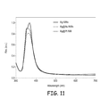
- FIG. 11 is a plot of light absorption covering a portion of the UV, the visible spectrum and a portion of the infrared for representative uncoated silver nanowires (solid line), platinum coated silver nanowires (dashed line) and gold coated silver nanowires (dotted line).
- FIG. 12 is a set of scanning electron micrograph images for a set of silver nanowires with a range of platinum coatings formed by direct deposition with coating amounts as specified by the amount of coating composition added in microliters during the coating process, in which lower magnification images are in the left column and higher magnification images are in the right column for uncoated silver nanowires at the top and increased amounts of platinum coated in lower images in each column (80 ⁇ L second image in each column, 120 ⁇ L third image of each column, and 160 ⁇ L fourth image in each column).
- FIG. 13 is a plot of light absorption for uncoated silver nanowires and silver nanowires with 5 different platinum coating thicknesses (40 ⁇ L Pt coating solution, 60 ⁇ L Pt coating solution, 80 ⁇ L Pt coating solution, 120 ⁇ L Pt coating solution and 160 ⁇ L Pt coating solution).
- FIG. 14A is an optical microscopic photograph of uncoated silver nanowires.
- FIG. 14B is an optical microscopic photograph of the uncoated silver nanowires of FIG. 14A after exposure to 150° C. conditions for 50 hours.
- FIG. 14C is an optical microscopic photograph of Pt coated silver nanowires.
- FIG. 14D is an optical microscopic photograph of the Pt coated silver nanowires of FIG. 14C after exposure to 150° C. conditions for 50 hours.
- FIG. 15 is a plot of change in the ratio of sheet resistance to initial sheet resistance as a function of time for transparent conductive films under 150° C. test conditions for uncoated silver nanowires and for Pt coated silver nanowires with 5 different quantities of Pt coating material.
- FIG. 16 is a plot of the ratio of sheet resistance to initial sheet resistance for three transparent conductive films without a polymer overcoat subjected to accelerated light fade conditions, in which film samples were a film formed with a fused metal nanostructured network formed with silver nanowires without a platinum coating, an unfused layer of platinum coated silver nanowires and a fused metal nanostructured network formed with platinum coated silver nanowires.
- FIG. 17 is a plot of the ratio of sheet resistance to initial sheet resistance for two transparent conductive films without a polymer overcoat subjected to 85° C. and 85% humidity, in which the samples are a film of unfused platinum coated silver nanowire and a fused metal nanostructured network formed from platinum coated silver nanowires.
- FIG. 18 is a plot of the ratio of sheet resistance to the initial sheet resistance as a function of time for four transparent conductive film samples under accelerated testing conditions with samples subjected to 85° C. and 85% humidity for samples of fused metal nanostructured networks formed with uncoated silver nanowires, or platinum coated silver nanowires with three different amounts of platinum coating as specified by the amount of platinum coating solution used (80 ⁇ L, 120 ⁇ L and 160 ⁇ L).
- FIG. 19 is a plot of the ratio of sheet resistance to the initial sheet resistance as a function of time for four transparent conductive film samples under accelerated testing conditions with samples subjected to 85° C. without added humidity for samples of fused metal nanostructured networks formed with uncoated silver nanowires, or platinum coated silver nanowires with three different amounts of platinum coating as specified by the amount of platinum coating solution used (80 ⁇ L, 120 ⁇ L and 160 ⁇ L).
- FIG. 20 is a plot of a set of cyclic voltammetry results showing current density as a function of voltage for four samples cycled from 1.1 V to ⁇ 1.1 V for samples of fused metal nanostructured networks covered with a polymer hardcoating formed with uncoated silver nanowires, or platinum coated silver nanowires with two different amounts of platinum coating as specified by the amount of platinum coating solution used (80 ⁇ L and 160 ⁇ L).
- Noble metal coated silver nanowires have been found to be very effective as substitutes for silver nanowires for the formation of transparent conductive films, especially with the formation of fused metal nanostructured networks. Under accelerated wear testing conditions, noble metal coated silver nanowires within transparent conductive layers exhibit significantly improved stability, when subjected to light, heat, chemical agents in the local environment and/or humidity, relative to corresponding structures with silver nanowires. Synthesis techniques are described in which either controlled galvanic replacement or direct deposition can be used to effectively deposit a uniform noble metal coating onto silver nanowires. In particular, direct deposition can be effectively used with room temperature processing, which can provide desirable processing advantages. Suitable metal binding ligands can be provided to stabilize the coating process to provide improved nanowire coatings.
- the noble metal coated nanowires can provide significant advantages for the formation of durable transparent conductive films.
- the noble metal coatings can significantly stabilize the films with respect to degradation over time in use while also improving or at least not degrading the optical properties of the films.
- the noble metal coatings can be consistent with the formation of fused metal conductive networks through the deposition of metal ions from solution as metal at the junctions of metal nanowires, which has been found to provide very desirable performance in transparent conductive films.
- Transparent electrically conductive elements e.g., films, of particular interest herein comprise a sparse metal conductive layer.
- the conductive layers are generally sparse to provide desired amount of optical transparency, so the coverage of the metal has very significant gaps over the layer of the conductive element.
- transparent electrically conductive films can comprise metal nanowires deposited along a layer where sufficient contact can be provided for electron percolation to provide suitable conduction pathways.
- the transparent electrically conductive film can comprise a fused metal nanostructured network, which has been found to exhibit desirable electrical and optical properties.
- Conductivity referenced herein refers to electrical conductivity unless specifically indicated otherwise. As described herein, the metal coated nanowires can be effectively incorporated into the transparent conductive elements.
- Sparse metal conductive layers regardless of the specific structures, are vulnerable to environmental assaults.
- the sparse feature implies that the structures are somewhat fragile. Assuming that the elements are appropriately protected from mechanical damage, the sparse metal conductive layers can be vulnerable to damage from various other sources, such as atmospheric oxygen, water vapor, oxidative stress, other corrosive chemicals in the local environment, such as sulfiding agents, light, heat, combinations thereof, and the like.
- degradation of properties of the transparent conductive structures should be within desired specifications, which in other words indicates that the transparent conductive layers provide suitable lifetimes for devices incorporating them. Accelerated wear studies are described below to test the transparent conductive films.
- noble metals refers to metals having a standard reduction potential greater than silver, so these would include, gold, platinum, iridium, rhodium, palladium and osmium, with a particular interest in gold and platinum.
- the noble metal coated nanowires are found to be suitable for forming sparse metal conductive layers with desirable electrical conductivity with good optical properties and significant stability with respect to accelerated wear testing. Using the synthesis techniques described herein, uniform coatings can be formed over intact silver nanowire cores. The results in the Examples demonstrate the deposition of smooth gold coatings and smooth platinum coatings onto silver nanowires.
- the amount of the coating deposited can be increased to relatively large values before the crystal structure of the coated metal begins to distort the surface structure.
- galvanic exchange it is difficult to deposit larger amounts of smooth coating onto the nanowires without damaging the underlying silver nanowire core due to the insulation of the underlying silver from oxidation effects as the coating is developed.
- direct deposition it is possible to deposit at least about 5 weight percent coating metal.
- gold coated nanowires and platinum coated nanowires can provide desired stability of sparse metal conductive layers including both fused metal nanostructured networks formed from the noble metal coated nanowires, and also unfused silver nanowire conductive layers.
- the Examples below demonstrate this improved stability of the transparent conductive films.
- Desirable methods for forming the metal coated nanowires can involve an improved version of galvanic replacement or the direct deposition of the coating metal.
- gold, platinum or other noble metal ions which generally are provided as metal ion complexes in solution, oxidize silver in the wires while being reduced to the elemental noble metal at elevated temperatures. So the reduced noble metal in elemental form replaces silver as the solid metal in the nanowires.
- the nanowire coating processes herein have been improved such that more uniform coatings can be deposited.
- the results in the Examples demonstrate the deposition of smooth gold coatings and smooth platinum coatings onto silver nanowires.
- strong binding ligands are introduced into the noble metal ion solution to control the reduction process. Appropriate strong binding ligands shift the free energy of the galvanic exchange such that no galvanic exchange takes place at room temperature, i.e., 20-23° C.
- the smooth coatings onto very uniform nanowires can result in coated nanowires with a standard deviation of diameter of no more than about 8 percent of the average diameter over the length of the nanowires.
- a reaction solution is formed with a dispersion of the silver nanowires, and a coating solution with the noble metal ions is gradually added to the reaction solution.
- the reaction solution is kept under reducing conditions.
- Hydrazine is a convenient reducing agent because the byproducts are nitrogen and water, although other reducing agents can be used as summarized below.
- the presence of hydrazine to maintain reducing conditions in the solution with the nanowires is believed to inhibit the oxidation of silver so that the coating process involves only the deposition of the noble metal from the solution.
- the direct coating method provides flexibility to control the amount of coating material deposited and for the deposition of a relatively thick coating without destabilizing the nanowire structure.
- control of the reaction in addition to the possible use of strong coordinating ligands and/or a polymer capping agent, can involve the gradual addition of the metal ion complexes of the coating metal as a metal ion source solution into the reaction solution.
- the reactions can be conveniently performed in aqueous solution with optionally some alcohol or other cosolvents.
- the coordinating ligand can be included in the solution with the metal ions.
- the metal ions can be provided in suitable complexes, such as the PtCl 6 ⁇ 2 complexes, and similar complexes can be used for other metals, such as AuCl 4 ⁇ .
- New metal complexes can be formed when stronger binding ligands are added to the coating solution, e.g., NO 2 ⁇ , which will complex with Pt 4+ by replacing Cl ⁇ .
- the strength of a ligand may not be completely predictable since it involves features of both the metal ion and the ligand.
- Complexes with halide ligands can generally be considered to be weak complexes.
- strong ligands can be identified in the context of galvanic exchange by the lack of measurable room temperature reaction of the coating solution. The free energy of the bonding strength of the ligand to the metal influences the effective reduction reaction of the metal and correspondingly the reduction potential.
- the ligand binding strength influences the energetics of the reaction, and the effect can be significant if the ligand binding strength is relatively strong. If the ligand binding to the noble metal ion is stronger than to the silver ion, a stronger binding ligand generally slows the noble metal deposition. In this way, the presence of a strong binding ligand can moderate the coating reactions, although the selection of the other reactants and processing conditions are also very significant.
- the amount of metal deposited in the coatings generally depends on the amount of added noble metal ions and the reaction conditions. As shown in the Examples, at least over a reasonable range of coating amounts, the stability of a transparent electrically conductive film increases with greater amounts of noble metal coatings.
- Metal coating of the nanowires can affect the sheet resistances of conductive films formed from the nanowires. Since silver metal has the highest electrical conductivity, coating with a noble metal may increase the sheet resistances, which may be balanced by the improved stability of the structure. Applicant has observed approximately equivalent sheet resistances in films formed with the noble metal coated silver nanowires with a slightly increased metal loading. The fusing process used by Applicant provides for a metal connection between the nanowires at points of contact or near approach.
- the noble metals generally absorb and scatter less visible light than silver so that in principle, a slightly higher loading of metal can be used for a particular optical transmittance and haze, and a higher loading of metal in a sparse metal conductive layer may decrease the electrical resistance.
- the use of noble metal coated silver nanowires as a material for forming the networks can result in desirable electrical conductivity and optical properties along with significantly improved stability.
- the coated wires show less haze and a more neutral color.
- Transparent electrically conductive elements e.g., films, of particular interest herein comprise a sparse metal conductive layer.
- the conductive layers are generally sparse to provide desired amount of optical transparency, so the coverage of the metal has very significant gaps over the layer of the conductive element.
- transparent electrically conductive films can comprise metal nanowires deposited along a layer where sufficient contact can be provided for electron percolation to provide suitable conduction pathways.
- the transparent electrically conductive film can comprise a fused metal nanostructured network, which has been found to exhibit desirable electrical and optical properties. It has been found that the noble metal coatings do not alter the ability to form desired fused metal nanostructured networks.
- halide ions can drive the fusing of metal nanowires to form fused metal nanostructures.
- Fusing agents comprising halide anions were introduced in various ways to successfully achieve the fusing with a corresponding significant drop in the electrical resistance.
- the fusing of metal nanowires with halide anions has been accomplished with vapors and/or solutions of acid halides as well as with solutions of halide salts. Fusing of metal nanowires with halide sources is described further in published U.S.
- the desirable inks to achieve effective single deposition inks that cure into fused nanostructured metal networks comprise a desired amount of metal nanowires to achieve appropriate loading of metal in the resulting film.
- the inks are stable prior to deposition of the ink and drying.
- the inks can comprise a reasonable amount of polymer binder that contributes to the formation of a stable conducting film for further processing.
- hydrophilic polymers have been found to be effective, such as cellulose or chitosan based polymers.
- Metal ions, as a source of metal for the fusing process can be supplied as a soluble metal salt.
- a single ink formulation provides for depositing a desired loading of metal as a film on the substrate surface and simultaneously providing constituents in the ink that induce the fusing process as the ink is dried under appropriate conditions.
- These inks can be referred to conveniently as fusing metal nanowire inks with the understanding that the fusing generally does not take place until drying.
- the inks generally comprise an aqueous solvent, which can further comprise an alcohol and/or other organic solvent in some embodiments.
- the inks can further comprise dissolved metal salts as a metal source for the fusing process. Without wanting to be limited by theory, it is believed that components of the ink, e.g., alcohol, or other organic compositions, reduce the metal ions from solution to drive the fusing process.
- a polymer binder can be provided to stabilize the film and to influence ink properties.
- the particular formulation of the ink can be adjusted to select ink properties suitable for a particular deposition approach and with specific coating properties on a substrate surface. As described further below, drying conditions can be selected to effectively perform the fusing process.
- noble metal coated nanowires are substituted for silver nanowires in the processing solutions for the formation of fused metal nanostructured networks, it has been found that the fusing process seems to proceed as expected.
- Silver ions can be used to provide the material for fusing the nanowires, although other metal ions can be supplied for the fusing metal if desired.
- other metal ions can be used for fusing, such as silver ions, copper ions, palladium ions, gold ions, tin ions, iron ions, cobalt ions, zinc ions, aluminum ions, platinum ions, nickel ions, cobalt ions, titanium ions, or combinations thereof.
- the results in the examples are consistent with the noble metal nanowires effectively fusing to form the conductive networks.
- silver is deposited at the junction points of the fused network based on the addition of silver ions in the solution.
- optical transparency is inversely related to the loading with higher loadings leading to a reduction in transparency, and haze generally increases with loading, although processing of the network can also significantly affect the optical properties.
- polymer binders and other additives can be selected to maintain good optical transparency.
- the transparent conductive films generally comprise several components or layers that contribute to the processability and/or the mechanical properties of the structure without detrimentally altering the optical properties.
- a polymer overcoat can be applied directly over the sparse metal conductive layer to stabilize the conductive layer.
- the sparse metal conductive layers can be designed to have desirable optical properties when incorporated into the transparent conductive films.
- the sparse metal conductive layer may or may not further comprise a polymer binder.
- a polymer undercoat layer or a polymer overcoat layer can comprise a stabilization composition to further stabilize the sparse metal conductive layer.
- references to thicknesses refer to average thicknesses over the referenced layer or film, and adjacent layers may intertwine at their boundaries depending on the particular materials.
- the total film structure can have a total transmission of visible light of at least about 85%, a haze of no more than about 2 percent and a sheet resistance of no more than about 250 ohm/sq.
- the transparent conductive layers generally can have their performance evaluated as formed, and performance can degrade with age of the film. In particular, electrical conductivity can degrade due to degradation of the metal network.
- the use of noble metal coated silver nanowires can achieve significant stabilization with respect to light and environmental assaults relative to equivalent conductive layers formed with silver nanowires formed without the metal coating. Stability of the conductive layer can be evaluated with accelerated wear test, and several versions are described below. Testing is performed with or without a polymer overcoat. In general, good stability is obtained for samples even without a polymer overcoat under fairly stringent test conditions. These results indicate that the noble metal coated silver nanowires can provide highly desirable stability for the formation of transparent conductive films for a range of products.
- the coated silver nanowires have a noble metal coating that can appear smooth under microscopic visualization of the coating with appropriate synthesis approaches for the coating.
- the processing can be adjusted to alter the amount of noble metal deposited. Based on improved coating methods, direct noble metal deposition or galvanic replacement can be used to deposit a smooth noble metal coating.
- noble metal coating can be controlled with selected ligands that moderate the noble metal deposition to form the coating as well as through the appropriate selection of other reactants and processing conditions, such as appropriate gradual addition of reactants. The controlling of the noble metal reduction has been found to facilitate the formation of a desirably smooth and uniform coating. As described herein, the noble metal coated silver nanowires provide excellent materials for formation of transparent conductive films.
- silver nanowires are available from Sigma-Aldrich (Missouri, USA), Cangzhou Nano-Channel Material Co., Ltd. (China), Blue Nano (North Carolina, USA), EMFUTUR (Spain), Seashell Technologies (California, USA), Aiden/C3Nano (Korea/USA), Nanocomposix (USA), Nanopyxis (Korea), K&B (Korea), ACS Materials (China), KeChuang Advanced Materials (China), and Nanotrons (USA).
- silver nanowires can also be synthesized using a variety of known synthesis routes or variations thereof. In general, any of these silver nanowires can be used for coating with the noble metals as describe herein.
- Silver in particular provides excellent electrical conductivity so it is desirable for the core of the coated metal nanowires to be silver.
- the metal nanowires can have an average length of at least a micron, in further embodiments, at least 2.5 microns and in other embodiments from about 5 microns to about 100 microns, although improved synthesis techniques developed in the future may make longer nanowires possible.
- An aspect ratio can be specified as the ratio of the average length divided by the average diameter, and in some embodiments, the nanowires can have an aspect ratio of at least about 25, in further embodiments from about 50 to about 5000 and in additional embodiments from about 100 to about 2000.
- the noble metals include gold, platinum, iridium, rhodium, palladium and osmium, with a particular interest in gold and platinum.
- the results suggest that the stability of conductive structures increases with increased amount of noble metal deposition, although stability may gradually plateau as more coating metal is provided.
- there are tradeoff with respect to coating with larger amounts of noble metals with respect to electrical conductivity, processing time and cost, stability and other parameters.
- a greater amount of noble metal can be deposited with a smooth coating and a stable silver metal core than can be obtained with galvanic exchange.
- the noble metal coating can be no more than about 55 wt %, in further embodiments from about 0.03 wt % to about 40 wt %, and in additional embodiments from about 0.9 wt % to about 25 wt %.
- the amount of coated metal generally ranges from about 0.02 atomic percent (at %) to about 35 at %, in further embodiments from about 0.1 at % to about 25 at %, in additional embodiments from about 0.5 at % to about 20 at % as a fraction of the total coated nanowire. Assuming that the coating is uniform and has a bulk material density, the coating thickness can be roughly estimated from the weight amount of the coating and the average parameters of the initial nanowires.
- Coating thicknesses can be estimated base on the weight of the coating material and the density of the coating metal.
- the smoothness of the coating can be determined using high resolution transmission electron micrographs (TEM). Using the smooth coating techniques developed herein, the coated nanowires can have a standard deviation
- the root mean square roughness of the coated nanowires can be no more than about 1 nm, in further embodiments no more than about 0.8 nm and in additional embodiments no more than about 0.6 nm.
- a first technique is based on galvanic exchange
- a second technique is based on direct deposition.
- the reducing agent for depositing the noble metal is the silver metal of the nanowires.
- the galvanic exchange reaction is driven with heat that provides activation energy to allow silver oxidation to reduce the noble metal.
- the galvanic replacement reaction can take place effectively in an aqueous solution.
- the noble metal is deposited directly from a reducing solution without oxidation of the silver nanowire.
- the noble metal ions can be added to a reactant solution comprising the silver nanowires and reducing agent. With both coating techniques, it can be desirable to have a polymer capping agent present.
- the reaction generally involves reacting complexed noble metal ions with silver nanowires in an aqueous solution in the presence of a capping polymer.
- a metal ion source solution comprising complexed noble metal ions can be added gradually to the reaction solution to moderate the reaction.
- the reaction solution generally can comprise initially dispersed silver nanowires, and a capping polymer in an aqueous solution.
- the reaction solution does not comprise a reducing agent.
- the reaction solution generally comprises silver nanowires in concentrations from about 0.0001 wt % to about 5 wt %, in further embodiments from about 0.02 wt % to about 3.5 wt % and in additional embodiments from about 0.03 wt % to about 2.5 wt %.
- the reaction solution can also comprise from about 0.005 wt % to about 2 wt % capping polymer, in further embodiments from about 0.01 wt % to about 1.5 wt % and in additional embodiments from about 0.02 wt % to about 1 wt % capping polymer.
- Polymer capping agents for silver nanowires are traditionally polyvinyl pyrrolidone (PVP), although in principle other polymers can be used, such as polyvinyl alcohol, polyacrylic acid, polyvinyl acetate, poly(vinyl pyrrolidone)-b-poly(vinyl alcohol), combinations thereof or the like.
- the solvent can be water, alcohol or blends of solvents with water (aqueous solvents) or alcohol.
- the silver nanowires can be provided in an alcohol dispersion that is then mixed with water to form the reaction solution.
- alcohol dispersion that is then mixed with water to form the reaction solution.
- the metal ion source solution can comprise metal ion complexes along with a suitably strong complexing ligand in an aqueous solution.
- the complexing ligand was ethylene diamine.
- suitable ligands include, for example, nitrite, diethyl amine, ethylene diamine, nitrilotriacetic acid, iminobis(methylene phosphonic acid), aminotris(methylene phosphonic acid), ethylene diamine tetraacetic acid (EDTA), 1,3-propylenediaminetetraacetic acid (1,3-PDTA), triethylene tetramine, tri(2-aminoethyl) amine, diethylenetriaminepentaacetic acid, 1,2-cyclohexanediaminotetraacetic acid, iminodiacetic acid, methyliminodiacetic acid, N-(2-acetamide) iminoacetic acid, N-(2-carboxyethyl) im
- Desirable strong binding ligands can be identified by the inhibition of galvanic exchange at room temperature with no measureable reaction taking place in 1 hour at room temperature under the range of reactant concentrations provided herein.
- the ligands that complex with the noble metal ions can lower their reduction potential to be smaller at room temperature than Ag oxidation potential, which can effectively eliminate the galvanic replacement at room temperature.
- the molar ratio of ligands to metal ions can be at least about 0.05, in further embodiments at least about 0.1, in additional embodiments at least about 0.5, in further embodiments at least about 0.75, in some embodiments at least about 0.80, and in other embodiments from about 0.85 to about 10.
- the metal ion source solution can comprise a noble metal ion concentration from about 1 ⁇ 10 ⁇ 8 M to about 10 M, in further embodiments from about 0.0001 M to about 5 M, and in additional embodiments from about 0.001 M to about 2.5 M.
- the noble metal ions can be added as a suitable salt, such as nitrate, sulfate, perchlorate, hexafluorophosphate, hexafluoroantimonate, and halides.
- the solvent can be water or other reasonable aqueous solution.
- the silver nanowire solution generally is heated to boiling and maintained at boiling throughout the reaction, although the reaction can be driven by heating to a somewhat lower temperature, e.g., generally at least about 40° C., in further embodiments at least about 60° C. and in additional embodiments at least about 75° C.
- the boiling point can change over the course of the reaction as lower boiling components boil off, so the temperature of the reaction solution can change over the course of the reaction if the heating element is set at a temperature over the boiling temperature of the lower boiling components when there is a solvent blend.
- the noble metal complex ion source solution can be added to the reaction solution over at least an hour, in further embodiments at least two hours and in additional embodiments at least 3 hours, which can be at a relatively constant rate over the time period.
- the reaction solution is generally mixed continuously during the reaction in a suitable container with a suitable mixing apparatus based on the reaction scale.
- the coated nanowires can be collected through the addition of acetone to the reaction solution.
- the modified solvent with the acetone results in the settling of the nanowires.
- the settled nanowires can be collected through filtering and/or centrifugation or the like, and the filtrate can be washed with water or other suitable solvent.
- the washed coated nanowires can be re-suspended in water, alcohol or solvent blend, and the washing process can be repeated with an acetone settling, filtering/centrifugation and washing steps. In some embodiments, the washing is performed a total of three times, although additional washing steps can be performed as desired.
- the washed nanowires can then be resuspended in water, alcohol or solvent blend with water and/or alcohol.
- the coating reaction mixture comprises a reducing agent that creates a reducing environment that drives the coating formation.
- Suitable reducing agents can include, for example, hydrazine, NaBH 4 , LiAlH 4 , ascorbic acid, oxalic acid, formic acid and the like.
- the coating process generally can be performed without the application of heat. Applicant has obtained desirable coating results using a coating solution comprising in addition to the reducing agent, a polymer capping agent and in some embodiments a coordinating ligand for the noble metal ion.
- Polymer capping agents for silver nanowires are traditionally polyvinyl pyrrolidone (PVP), although in principle other polymers can be used, such as polyvinyl alcohol, polyacrylic acid, polyvinyl acetate, poly(vinyl pyrrolidone)-b-poly(vinyl alcohol), combinations thereof or the like.
- PVP polyvinyl pyrrolidone
- the selection of an appropriate ligand has been found to be useful with respect to obtaining a smooth coating.
- the direct coating deposition process can be controlled for the formation of smooth coating, for example, through the use of a coordination ligand, the gradual addition of the noble metal ions and control of other reaction parameters.
- the ligand complex with the noble metal can lower its reduction potential and reduce or eliminate the galvanic reaction in the presence of reducing agent.
- the coordinating ligand can be added in significant molar excess relative to the noble metal ions, although a ligand to metal ion ratio less than about 1, generally at least about 0.05, can be beneficial with respect to the coating.
- additional molar ratios of ligands to metal ions between about 0.05 and about 1 are contemplated and are within the present disclosure.
- the experiments have used sodium nitrite effectively, but other coordinating ligands other than nitrite, such as ethylene diamine, nitrilotriacetic acid, iminobis(methylene phosphonic acid), histidine, combinations thereof, and the like, can in principle be used effectively.
- the ligands for stabilizing direct deposition may be a somewhat different group than the ligands that stabilize galvanic exchange, from a present practical perspective the desirable ligands for galvanic exchange are also the desirable ligands for direct deposition.
- suitable ligands to control the direct deposition process include, for example, nitrite, ethylene diamine, diethyl amine, nitrilotriacetic acid, iminobis(methylene phosphonic acid), triethylene tetramine, tri(2-amnoethyl) amine, histidine, aminotris(methylene phosphonic acid), ethylene diamine tetraacetic acid (EDTA), 1,3-propylenediaminetetraacetic acid (1,3-PDTA), triethylene tetramine, tri(2-aminoethyl) amine, diethylenetriaminepentaacetic acid, 1,2-cyclohexanediaminotetraacetic acid, iminodiacetic acid, methyliminodiacetic acid, N-(2-acetamide) iminoacetic acid, N-(2-carboxyethyl) iminodiacetic acid, N-(2-carboxymethyl)imino dipropionic acid, picolinic acid,
- a reaction solution is formed with the silver nanowires, the polymer capping agent, and the reducing agent in a solvent, and a coating solution is added gradually that comprises noble metal ions, additional capping polymer, and ligands in a solvent.
- the reaction solution generally comprises silver nanowires in concentrations from about 0.0001 wt % to about 5 wt %, in further embodiments from about 0.02 wt % to about 3.5 wt % and in additional embodiments from about 0.03 wt % to about 2.5 wt %.
- the reacting solution can comprise from about 0.005 wt % to about 2 wt % capping polymer, in further embodiments from about 0.01 wt % to about 1.5 wt % and in additional embodiments from about 0.02 wt % to about 1 wt % capping polymer.
- the reaction solution generally also comprises from about 1 micromolar ( ⁇ M) reducing agent to about 1 millimolar (mM), in further embodiments from about 2 ⁇ M to about 500 ⁇ M and in additional embodiments from about 3 ⁇ M to about 250 ⁇ M reducing agent.
- the solution is generally water, alcohols, such as ethanol, isopropanol, glycols and the like, or blends of water (aqueous), alcohol and other solvents, and suitable cosolvents can be selected that do not destabilize the nanowire dispersions.
- a coating solution that can function as the metal complex ion source can be gradually added to the reaction solution to effectuate the coating process.
- the total amount of coating metal supplied as ions in the coating solution can be selected to provide the desired noble metal coating thickness.
- the coating solution can comprise noble ions in amounts generally ranging from about 0.02 atomic percent (at %) to about 35 at %, in further embodiments from about 0.1 at % to about 30 at %, in additional embodiments from about 0.5 at % to about 25 at % as a fraction of the total coated nanowire.
- the noble metal ions can be supplied as a suitable salt, which may comprise weakly bound ligands. Suitable noble metal salts include, for example, nitrate, sulfate, perchlorate, hexafluorophosphate, hexafluoroantimonate, and halides.
- the coating solution can comprise 0.00005 M to about 0.05 M, in further embodiments from about 0.0001 M to about 0.025 M and in additional embodiments from about 0.0002 M to about 0.01 M noble metal ions.
- the coordinating ligand is generally included in significant molar excess.
- the molar ratio of ligands to metal ions can be at least about 0.05, in further embodiments at least about 0.1, in additional embodiments at least about 0.5, in further embodiments at least about 0.75, in some embodiments at least about 0.8, and in other embodiments from about 0.85 to about 10.
- the coating solution can also comprise capping polymer from about 0.001 wt % to about 5 wt % capping polymer, in further embodiments from about 0.002 wt % to about 1.5 wt % and in additional embodiments from about 0.005 wt % to about 1 wt % capping polymer.
- the coating solution generally is also aqueous, such as water solvent.
- the rate of addition of addition of the coating solution can be adjusted to obtain uniform coating properties.
- the coating solution can be added at room temperature. Generally, the coating solution depending on scale can be added over a period from about 5 minutes to about 5 hours, in further embodiments from about 7 minutes to about 4.5 hours, and in additional embodiments from about 10 minutes to about 4 hours. A person of ordinary skill in the art will recognize that additional ranges of time within the explicit ranges of process times above are conceived and are within the present disclosure.
- the coating solution can be added at an approximately constant rate over the addition period.
- the reaction solution is generally mixed continuously during the reaction in a suitable container with a suitable mixing apparatus based on the reaction scale. Direct coating can have scale up advantages and avoidance of limits on amount of coating deposition suitable by galvanic replacement.
- the coated nanowires can be collected through the addition of acetone to the reaction solution.
- the modified solvent with the acetone results in the settling of the nanowires.
- the settled nanowires can be collected through filtering and/or centrifugation or the like, and the filtrate can be washed with water or other suitable solvent.
- the washed coated nanowires can be re-suspended in water, alcohol or solvent blend, and the washing process can be repeated with an acetone settling, filtering/centrifugation, and washing steps. In some embodiments, the washing is performed a total of three times, although additional washing steps can be performed as desired.
- the washed nanowires can then be re-suspended in water, alcohol or solvent blend with water and/or alcohol.
- the transparent electrically conductive structures or films generally comprise a sparse metal conductive layer that provides the electrical conductivity without significantly adversely altering the optical properties and various additional layers that provide mechanical support as well as protection of the conductive element.
- the sparse metal conductive layer is extremely thin and correspondingly susceptible to damage by mechanical and other abuses.
- the sparse metal conductive layer can be formed on a substrate that can have one or more layers in the structure of the substrate.
- the substrate generally can be identified as a self-supporting film or sheet structure.
- a thin solution processed layer, referred to as an undercoat can be optionally placed along the top surface of the substrate film and immediately under the sparse metal conductive layer.
- the sparse metal conductive can be coated with additional layers that provide some protection on the side of the sparse metal conductive layer opposite the substrate.
- the electrically conductive structure can be placed in either orientation in the final product, i.e., with the substrate facing outward to the substrate against the surface of the product supporting the electrically conductive structure.
- representative transparent conductive film 100 comprises a substrate 102 , undercoat layer 104 , sparse metal conductive layer 106 , overcoat layer 108 , optically clear adhesive layer 110 and protective surface layer 112 , although not all embodiments include all layers.
- a transparent conductive film generally comprises a sparse metal conductive layer and at least one layer on each side of the sparse metal conductive layer.
- the total thickness of the transparent conductive film can generally have a thickness from 10 microns to about 3 millimeters (mm), in further embodiments from about 15 microns to about 2.5 mm and in other embodiments from about 25 microns to about 1.5 mm.
- the length and width of the film as produced can be selected to be appropriate for a specific application so that the film can be directly introduced for further processing into a product.
- a width of the film can be selected for a specific application, while the length of the film can be long with the expectation that the film can be cut to a desired length for use.
- the film can be in long sheets or a roll.
- the film can be on a roll or in another large standard format and elements of the film can be cut according to a desired length and width for use.
- Substrate 102 generally comprises a durable support layer formed from an appropriate polymer or polymers.
- the substrate can has a thickness from about 20 microns to about 1.5 mm, in further embodiments from about 35 microns to about 1.25 mm and in additional embodiments from about 50 microns to about 1 mm.
- additional ranges of thicknesses of the substrate within the explicit ranges above are contemplated and are within the present disclosure.
- Suitable optically clear polymers with very good transparency, low haze and good protective abilities can be used for the substrate.
- Suitable polymers include, for example, polyethylene terephthalate (PET), polyethylene naphthalate (PEN), polyacrylate, poly(methyl methacrylate), polyolefin, polyvinyl chloride, fluoropolymers, polyamide, polyimide, polysulfone, polysiloxane, polyetheretherketone, polynorbornene, polyester, polystyrene, polyurethane, polyvinyl alcohol, polyvinyl acetate, acrylonitrile-butadiene-styrene copolymer, cyclic olefin polymer, cyclic olefin copolymer, polycarbonate, copolymers thereof or blend thereof or the like.
- PET polyethylene terephthalate
- PEN polyethylene naphthalate
- polyacrylate poly(methyl methacrylate)
- polyolefin polyvinyl chloride
- fluoropolymers fluoropolymers
- polyamide polyimide
- Suitable commercial polycarbonate substrates include, for example, MAKROFOL SR243 1-1 CG, commercially available from Bayer Material Science; TAP® Plastic, commercially available from TAP Plastics; and LEXANTM 8010CDE, commercially available from SABIC Innovative Plastics.
- Protective surface layer 112 can independently have a thickness and composition covering the same thickness ranges and composition ranges as the substrate as described in this paragraph above.
- Optional undercoat 104 and/or optional overcoat 108 can be placed respectively under or over sparse metal conductive layer 106 .
- Optional coatings 104 , 108 can comprise a curable polymer, e.g., heat curable or radiation curable polymers. Suitable polymers for coatings 104 , 108 are described below as binders for inclusion in the metal nanowire inks, and the list of polymers, corresponding cross linking agents and additives apply equally to optional coatings 104 , 108 without repeating the discussion explicitly here. Some of the binder polymers are referred to as hardcoat polymers due to abrasion resistance, and hardcoat polymers can be desirable in particular for overcoat 108 to provide abrasion resistance.
- Coatings 104 , 108 can have a thickness from about 25 nm to about 2 microns, in further embodiments from about 40 nm to about 1.5 microns and in additional embodiments from about 50 nm to about 1 micron.
- a person of ordinary skill in the art will recognize that additional ranges of overcoat thickness within the explicit ranges above are contemplated and are within the present disclosure.
- Optional optically clear adhesive layer 110 can have a thickness from about 10 microns to about 300 microns, in further embodiments from about 15 microns to about 250 microns and in other embodiments from about 20 microns to about 200 microns.
- Suitable optically clear adhesives can be contact adhesives.
- Optically clear adhesives include, for example, coatable compositions and adhesive tapes. UV curable liquid optically clear adhesives are available based on acrylic or polysiloxane chemistries.
- Suitable adhesive tapes are available commercially, for example, from Lintec Corporation (MO series); Saint Gobain Performance Plastics (DF713 series); Nitto Americas (Nitto Denko) (LUCIACS CS9621T and LUCIAS CS9622T); DIC Corporation (DAITAC LT series OCA, DAITAC WS series OCA and DAITAC ZB series); PANAC Plastic Film Company (PANACLEAN series); Minnesota Mining and Manufacturing (3M, Minnesota, USA—product numbers 8146, 8171, 8172, 8173 and similar products) and Adhesive Research (for example product 8932).
- the amount of nanowires delivered onto the substrate for sparse metal conductive layer 106 can involve a balance of factors to achieve desired amounts of transparency and electrical conductivity. While thickness of the nanowire network can in principle be evaluated using scanning electron microscopy, the network can be relatively sparse to provide for optical transparency, which can complicate the measurement.
- the sparse metal conductive structure e.g., fused metal nanowire network, would have an average thickness of no more than about 5 microns, in further embodiments no more than about 2 microns and in other embodiments from about 10 nm to about 500 nm.
- the sparse metal conductive structures are generally relatively open structures with significant surface texture on a submicron scale.
- the loading levels of the nanowires can provide a useful parameter of the network that can be readily evaluated, and the loading value provides an alternative parameter related to thickness.
- loading levels of nanowires onto the substrate is generally presented as milligrams of nanowires for a square meter of substrate.
- the nanowire networks can have a loading from about 0.1 milligrams (mg)/m 2 to about 300 mg/m 2 , in further embodiments from about 0.5 mg/m 2 to about 200 mg/m 2 , and in other embodiments from about 1 mg/m 2 to about 150 mg/m 2 .
- mg milligrams
- a person of ordinary skill in the art will recognize that additional ranges of thickness and loading within the explicit ranges above are contemplated and are within the present disclosure. If the sparse metal conductive layer is patterned, the thickness and loading discussion applies only to the regions where metal is not excluded or significantly diminished by the patterning process.
- layers 102 , 104 , 106 , 108 , 110 , 112 can be subdivided into sub-layers, for example, with different compositions from other sub-layers.
- sub-layers may or may not be processed similarly to other sub-layers within a particular layer, for example, one sub-layer can be laminated while another sub-layer can be coated and cured.
- Stabilization compositions can be placed in appropriate layers to stabilize the sparse metal conductive layers.
- the sparse metal conductive layers comprise fused nanostructured metal networks
- the sparse metal conductive layer itself as formed may not comprise a stabilization compound since the presence of such compounds can inhibit the chemical fusing process.
- stabilization compounds can be included in an optically clear adhesive composition. However, it has been found that the stabilization compounds can be included effectively in a coating layer, which can correspondingly be made relatively thin while still providing effective stabilization.
- an undercoat and/or overcoat can comprise a stabilization composition that can provide desirable protection, and certain classes of optically clear adhesives and/or barrier layers can also provide valuable protection from light, heat, chemicals and other environmental damage. While the focus herein is on environmental assaults from humid air, heat and light, polymer sheets used to protect the conductive layers from these environmental assaults can also provide protection from contact and the like.
- stabilization compounds have been proposed for silver nanowire conductive layers.
- corrosion inhibitors such as phenolic compounds (bis(4-hydroxyphenol)sulphone, 2,6-di-tert-butylphenol or resorcinol) are proposed as stabilization compounds in published U.S. patent application 2014/0205845 to Philip, Jr. et al., entitled “Stabilization Agents for Transparent Conductive Films,” incorporated herein by reference.
- Mercaptotetrazoles, mercaptotriazoles and their tautomers are described as stabilization compounds in published U.S. patent application 2014/0170407 to Zou et al., entitled “Anticorrosion Agents for Transparent Conductive Film,” incorporated herein by references.
- a coating layer can comprise a stabilization compound in a concentration from about 0.1 weight percent (wt %) to about 8 wt %, in further embodiments from about 0.25 wt % to about 6 wt % and in additional embodiments from about 0.5 wt % to about 4 wt %.
- wt % weight percent
- a coating layer can comprise a stabilization compound in a concentration from about 0.1 weight percent (wt %) to about 8 wt %, in further embodiments from about 0.25 wt % to about 6 wt % and in additional embodiments from about 0.5 wt % to about 4 wt %.
- This ability to pattern based on fusing provides significant additional patterning options based on selective fusing of the nanowires, for example, through the selective delivery of a fusing solution or vapor. Patterning based on selective fusing of metal nanowires is described in the '833 application above.
- a fused metal nanostructured network can form conductive patterns along a substrate surface 120 with a plurality of electrically conductive pathways 122 , 124 , and 126 surrounded by electrically resistive regions 128 , 130 , 132 , 134 , as shown in FIG. 2 .
- the fused area correspond with three distinct electrically conductive regions corresponding with electrically conductive pathways 122 , 124 , and 126 .
- three independently connected conductive regions have been illustrated in FIG. 2 , it is understood that patterns with two, four or more than 4 conductive independent conductive pathways or regions can be formed as desired.
- fairly intricate patterns can be formed with a large number of elements.
- very fine patterns can be formed with highly resolved features.
- the shapes of the particular conductive regions can be selected as desired.
- the transparent conductive film is generally built up around the sparse metal conductive element which is deposited to form the functional feature of the film.
- Various layers are coated, laminated or otherwise added to the structure using appropriate film processing approaches. As described herein, the nature of the layers can significant can alter the long term performance of the transparent conductive film.
- the deposit of the sparse metal conductive layer is described further below in the context of a fused metal nanostructured layers, but un-fused metal nanowire coatings can be similarly deposited except that the fusing components are absent.
- the sparse metal conductive layer generally is solution coated onto a substrate, which may or may not have a coating layer on top of the substrate that then forms an undercoat adjacent the sparse metal conductive layer.
- An overcoat can be solution coated onto the sparse metal conductive layer in some embodiments.
- Crosslinking with application of UV light, heat or other radiation, can be performed to crosslink polymer binders in the coating layers and/or the sparse metal conductive layer, which can be performed in one step or multiple steps.
- a stabilization compound can be incorporated into the coating solution for forming a coating layer.
- the coating precursor solution can comprise 0.001 weight percent (wt %) to about 0.1 wt % stabilization compound, in further embodiments from about 0.002 wt % to about 0.05 wt %, in additional embodiments from about 0.003 wt % to about 0.04 wt % and in other embodiments from about 0.003 wt % to about 0.025 wt % stabilization compound.
- wt % weight percent
- stabilization compound in a coating solution within the explicit ranges above are contemplated and are within the present disclosure.
- An optically clear adhesive layer can be laminated or otherwise applied to the sparse metal conductive layer with or without an overcoat layer(s) that becomes located adjacent the optically clear adhesive.
- a stabilization composition can be associated with an optically clear adhesive through the contact of a solution comprising the stabilization compound with the optically clear adhesive, such as by spraying or dipping a solution of the stabilization compound with the optically clear adhesive.
- the stabilization compound can be incorporated into the adhesive composition during the manufacture of the adhesive.
- an additional protective film can be applied over the optically clear adhesive layer, or a protective polymer film can be laminated or otherwise applied to an overcoat or directly to the sparse metal conductive layer without an intervening optically conductive adhesive.
- a protective film can be placed over the optically clear adhesive to form a further protective layer.
- Suitable protective films can be formed of similar materials as described for the substrate material, or specific commercial barrier films can be used.
- the protective films can be formed from polyester sheets with coatings.
- Hard coated polyester sheets are commercially available, in which the hard coats are crosslinked acrylic polymers or other crosslinked polymers. Hard coated polyester sheets are desirable due to a relatively low cost and desirable optical properties, such as a high transparency and low haze.
- Thicker hard coated polyester films can be used to increase their barrier function, such as sheets having a thickness from about 15 microns to about 200 microns and in further embodiments from about 20 microns to about 150 microns.
- additional ranges of hard coated polyester films are contemplated and are within the present disclosure.
- the results presented herein indicate that a combination of stabilization features can effectively provide a high degree of stabilization as determined with selected accelerated age testing.
- the inclusion of noble metal coated silver nanowires to form the sparse metal conductive layer can be combined with an optically clear adhesive with a polyester carrier film and/or a protective cover film to stabilize the sparse metal conductive layer and maintain a desirably low sheet resistance.
- Optically clear adhesive layers and thicker protective films covering the sparse metal conductive layer can be formed with holes or the like in appropriate locations to provide for electrical connections to the conductive layer.
- various polymer film processing techniques and equipment can be used to the processing of these polymer sheets, and such equipment and techniques are well developed in the art, and future developed processing techniques and equipment can be correspondingly adapted for the materials herein.
- Sparse metal conductive layers are generally formed from metal nanowires. With sufficient loading and selected nanowire properties, reasonable electrical conductivity can be achieved with the nanowires with corresponding appropriate optical properties. It is expected that the stabilized film structures described herein can yield desirable performance for films with various sparse metal conductive structures. However, particularly desirable properties have been achieved with fused metal nanostructured networks.
- the metal nanowire processing can be accomplished through deposition of two inks with the first ink comprising the metal nanowires and the second ink comprising a fusing composition, or through the deposition of an ink that combines the fusing elements into the metal nanowire dispersion.
- the inks may or may not further comprise additional processing aids, binders or the like.
- Suitable patterning approaches can be selected to be suitable for the particular ink system.
- one or more solutions or inks for the formation of the metal nanostructured network can collectively comprise well dispersed metal nanowires, a fusing agent, and optional additional components, for example, a polymer binder, a crosslinking agent, a wetting agent, e.g., a surfactant, a thickener, a dispersant, other optional additives or combinations thereof.
- the solvent for the metal nanowire ink and/or the fusing solution if distinct from the nanowire ink can comprise an aqueous solvent, an organic solvent or mixtures thereof.
- suitable solvents include, for example, water, alcohols, ketones, esters, ethers, such as glycol ethers, aromatic compounds, alkanes, and the like and mixtures thereof.
- Specific solvents include, for example, water, ethanol, isopropyl alcohol, isobutyl alcohol, tertiary butyl alcohol, methyl ethyl ketone, glycol ethers, methyl isobutyl ketone, toluene, hexane, ethyl acetate, butyl acetate, ethyl lactate, PGMEA (2-methoxy-1-methylethylacetate), or mixtures thereof.
- the solvent should be selected based on the ability to form a good dispersion of metal nanowires, the solvents should also be compatible with the other selected additives so that the additives are soluble in the solvent.
- the solvent or a component thereof may or may not be a significant component of the fusing solution, such as alcohols and can be selected accordingly if desired.
- the nanowires can be formed from a range of metals, such as silver, gold, indium, tin, iron, cobalt, platinum, palladium, nickel, cobalt, titanium, copper and alloys thereof, which can be desirable due to high electrical conductivity.
- the noble metal nanowires described in detail above can be introduced into the sparse metal conductive layers.
- the metal nanowire ink in either a one ink or two ink configuration, can include from about 0.01 to about 1 weight percent metal nanowires, in further embodiments from about 0.02 to about 0.75 weight percent metal nanowires and in additional embodiments from about 0.04 to about 0.5 weight percent metal nanowires.
- Polymer binders and the solvents are generally selected consistently such that the polymer binder is soluble or dispersible in the solvent.
- the metal nanowire ink generally comprises from about 0.02 to about 5 weight percent binder, in further embodiments from about 0.05 to about 4 weight percent binder and in additional embodiments from about 0.1 to about 2.5 weight percent polymer binder.
- the polymer binder comprises a crosslinkable organic polymer, such as a radiation crosslinkable organic polymer and/or a heat curable organic binder.
- the metal nanowire ink can comprise in some embodiments from about 0.0005 wt % to about 1 wt % of a crosslinking agent, in further embodiments from about 0.002 wt % to about 0.5 wt % and in additional embodiments from about 0.005 to about 0.25 wt %.
- the nanowire ink can optionally comprise a rheology modifying agent or combinations thereof.
- the ink can comprise a wetting agent or surfactant to lower the surface tension, and a wetting agent can be useful to improve coating properties.
- the wetting agent generally is soluble in the solvent.
- the nanowire ink can comprise from about 0.01 weight percent to about 1 weight percent wetting agent, in further embodiments from about 0.02 to about 0.75 weight percent and in other embodiments from about 0.03 to about 0.6 weight percent wetting agent.
- a thickener can be used optionally as a rheology modifying agent to stabilize the dispersion and reduce or eliminate settling.
- the nanowire ink can comprise optionally from about 0.05 to about 5 weight percent thickener, in further embodiments from about 0.075 to about 4 weight percent and in other embodiments from about 0.1 to about 3 weight percent thickener.
- a range of polymer binders can be suitable for dissolving/dispersing in a solvent for the metal nanowires, and suitable binders include polymers that have been developed for coating applications.
- Hard coat polymers e.g., radiation curable coatings
- Suitable classes of radiation curable polymers and/or heat curable polymers include, for example, polyurethanes, acrylic resins, acrylic copolymers, cellulose ethers and esters, other water insoluble structural polysaccharides, polyethers, polyesters, epoxy containing polymers, and mixtures thereof.
- Examples of commercial polymer binders include, for example, NEOCRYL® brand acrylic resin (DMS NeoResins), JONCRYL® brand acrylic copolymers (BASF Resins), ELVACITE® brand acrylic resin (Lucite International), SANCURE® brand urethanes (Lubrizol Advanced Materials), cellulose acetate butyrate polymers (CAB brands from EastmanTM Chemical), BAYHYDROLTM brand polyurethane dispersions (Bayer Material Science), UCECOAT® brand polyurethane dispersions (Cytec Industries, Inc.), MOWITOL® brand polyvinyl butyral (Kuraray America, Inc.), cellulose ethers, e.g., ethyl cellulose or hydroxypropyl methyl cellulose, other polysaccharide based polymers such as Chitosan and pectin, synthetic polymers like polyvinyl acetate, and the like.
- DMS NeoResins JONCRYL® brand acrylic copo
- the polymer binders can be self-crosslinking upon exposure to radiation, and/or they can be crosslinked with a photoinitiator or other crosslinking agent.
- photocrosslinkers may form radicals upon exposure to radiation, and the radicals then induce crosslinking reactions based on radical polymerization mechanisms.
- Suitable photoinitiators include, for example, commercially available products, such as IRGACURE® brand (BASF), GENOCURETM brand (Rahn USA Corp.), and DOUBLECURE® brand (Double Bond Chemical hid., Co, Ltd.), combinations thereof or the like.
- Wetting agents can be used to improve the coatability of the metal nanowire inks as well as the quality of the metal nanowire dispersion.
- the wetting agents can lower the surface energy of the ink so that the ink spreads well onto a surface following coating.
- Wetting agents can be surfactants and/or dispersants.
- Surfactants are a class of materials that function to lower surface energy, and surfactants can improve solubility of materials.
- Surfactants generally have a hydrophilic portion of the molecule and a hydrophobic portion of the molecule that contributes to its properties.
- a wide range of surfactants, such as nonionic surfactants, cationic surfactant, anionic surfactants, zwitterionic surfactants, are commercially available.
- non-surfactant wetting agents e.g., dispersants
- Suitable commercial wetting agents include, for example, COATOSILTM brand epoxy functionalized silane oligomers (Momentum Performance Materials), SILWETTM brand organosilicone surfactant (Momentum Performance Materials), THETAWETTM brand short chain non-ionic fluorosurfactants (ICT Industries, Inc.), ZETASPERSE® brand polymeric dispersants (Air Products Inc.), SOLSPERSE® brand polymeric dispersants (Lubrizol), XOANONS WE-D545 surfactant (Anhui Xoanons Chemical Co., Ltd), EFKATM PU 4009 polymeric dispersant (BASF), MASURF FP-815 CP, MASURF FS-910 (Mason Chemicals), NOVECTM FC-4430 fluor
- Thickeners can be used to improve the stability of the dispersion by reducing or eliminating settling of the solids from the metal nanowire inks. Thickeners may or may not significantly change the viscosity or other fluid properties of the ink. Suitable thickeners are commercially available and include, for example, CRAYVALLACTM brand of modified urea such as LA-100 (Cray Valley Acrylics, USA), polyacrylamide, THIXOLTM 53L brand acrylic thickener, COAPURTM 2025, COAPURTM 830W, COAPURTM 6050, COAPURTM XS71 (Coatex, Inc.), BYK® brand of modified urea (BYK Additives), Acrysol DR 73, Acrysol RM-995, Acrysol RM-8W (Dow Coating Materials), Aquaflow NHS-300, Aquaflow XLS-530 hydrophobically modified polyether thickeners (Ashland Inc.), Borchi Gel L 75 N, Borchi Gel PW25 (OMG Borchers
- Additional additives can be added to the metal nanowire ink, generally each in an amount of no more than about 5 weight percent, in further embodiments no more than about 2 weight percent and in further embodiments no more than about 1 weight percent.
- Other additives can include, for example, anti-oxidants, UV stabilizers, defoamers or anti-foaming agents, anti-settling agents, viscosity modifying agents, or the like.
- fusing of the metal nanowires can be accomplished through various agents. Without wanting to be limited by theory, the fusing agents are believed to mobilize metal ions, and the free energy seems to be lowered in the fusing process. Excessive metal migration or growth may lead in some embodiments to a degeneration of the optical properties, so desirable results can be achieved through a shift in equilibrium in a reasonably controlled way, generally for a short period of time, to generate sufficient fusing to obtain desired electrical conductivity while maintaining desired optical properties.
- initiation of the fusing process can be controlled through a partial drying of the solutions to increase concentrations of the components, and quenching of the fusing process can be accomplished, for example, through rinsing or more completing drying of the metal layer.
- the fusing agent can be incorporated into a single ink along with the metal nanowires.
- the one ink solution can provide appropriate control of the fusing process.
- a process in which a sparse nanowire film is initially deposited and subsequent processing with or without depositing another ink provides for the fusing of the metal nanowires into a metal nanostructured network, which is electrically conducting.
- the fusing process can be performed with controlled exposure to a fusing vapor and/or through the deposition of a fusing agent in solution.
- Sparse metal conductive layers are generally formed on a selected substrate surface.
- the as deposited nanowire film is dried to remove the solvent. Processing can be adapted for patterning of the film as described further below.
- any reasonable deposition approach can be used, such as dip coating, spray coating, knife edge coating, bar coating, Meyer-rod coating, slot-die, gravure printing, spin coating or the like.
- the ink can have properties, such as viscosity, adjusted appropriately with additives for the desired deposition approach.
- the deposition approach directs the amount of liquid deposited, and the concentration of the ink can be adjusted to provide the desired loading of metal nanowires on the surface. After forming the coating with the dispersion, the sparse metal conductive layer can be dried to remove the liquid.
- the films can be dried, for example, with a heat gun, an oven, a thermal lamp or the like, although the films that can be air dried can be desired in some embodiments.
- the films can be heated to temperatures from about 50° C. to about 150° C. during drying.
- the films can be washed one or more times, for example, with an alcohol or other solvent or solvent blend, such as ethanol or isopropyl alcohol, to removed excess solids to lower haze.
- Patterning can be achieved in several convenient ways. For example, printing of the metal nanowires can directly result in patterning. Additionally or alternatively, lithographic techniques can be used to remove portions of the metal nanowires, prior to or after fusing, to form a pattern.
- the fused metal nanostructured networks can provide low electrical resistance while providing good optical properties.
- the films can be useful as transparent conductive electrodes or the like.
- the transparent conductive electrodes can be suitable for a range of applications such as electrodes along light receiving surfaces of solar cells.
- the films can be patterned to provide electrically conductive patterns formed by the film.
- the substrate with the patterned film generally has good optical properties at the respective portions of the pattern.
- Electrical resistance of thin films can be expressed as a sheet resistance, which is reported in units of ohms per square ( ⁇ / ⁇ or ohms/sq) to distinguish the values from bulk electrical resistance values according to parameters related to the measurement process. Sheet resistance of films is generally measured using a four point probe measurement or another suitable process.
- the fused metal nanostructured networks can have a sheet resistance of no more than about 300 ohms/sq, in further embodiments no more than about 200 ohms/sq, in additional embodiments no more than about 100 ohms/sq and in other embodiments no more than about 60 ohms/sq.
- sheet resistance can be reduced by increasing the loading of nanowires, but an increased loading may not be desirable from other perspectives, and metal loading is only one factor among many for achieving low values of sheet resistance.
- optical transparency is inversely related to the loading with higher loadings leading to a reduction in transparency, although processing of the network can also significantly affect the transparency.
- polymer binders and other additives can be selected to maintain good optical transparency.
- the optical transparency can be evaluated relative to the transmitted light through the substrate. For example, the transparency of the conductive film described herein can be measured by using a UV-Visible spectrophotometer and measuring the total transmission through the conductive film and support substrate. Transmittance is the ratio of the transmitted light intensity (I) to the incident light intensity (I o ).
- the transmittance through the film can be estimated by dividing the total transmittance (T) measured by the transmittance through the support substrate (T sub ).
- the reported total transmissions can be corrected to remove the transmission through the substrate to obtain transmissions of the film alone. While it is generally desirable to have good optical transparency across the visible spectrum, for convenience, optical transmission can be reported at 550 nm wavelength of light. Alternatively or additionally, transmission can be reported as total transmittance from 400 nm to 700 nm wavelength of light, and such results are reported in the Examples below.
- the measurements of 550 nm transmittance and total transmittance from 400 nm to 700 nm are not qualitatively different.
- the film formed by the fused network has a total transmittance (TT %) of at least 80%, in further embodiments at least about 85%, in additional embodiments, at least about 90%, in other embodiments at least about 94% and in some embodiments from about 95% to about 99%.
- Transparency of the films on a transparent polymer substrate can be evaluated using the standard ASTM D1003 (“Standard Test Method for Haze and Luminous Transmittance of Transparent Plastics”), incorporated herein by reference.
- the fused metal networks can also have low haze along with high transmission of visible light while having desirably low sheet resistance.
- Haze can be measured using a hazemeter based on ASTM D1003 referenced above, and the haze contribution of the substrate can be removed to provide haze values of the transparent conductive film.
- the sintered network film can have a haze value of no more than about 1.2%, in further embodiments no more than about 1.1%, in additional embodiments no more than about 1.0% and in other embodiments from about 0.9% to about 0.2%. As described in the Examples, with appropriately selected silver nanowires very low values of haze and sheet resistance have been simultaneously achieved.
- the loading can be adjusted to balance the sheet resistance and the haze values with very low haze values possible with still good sheet resistance values. Specifically, haze values of no more than 0.8%, and in further embodiments from about 0.4% to about 0.7%, can be achieved with values of sheet resistance of at least about 45 ohms/sq. Also, haze values of 0.7% to about 1.2%, and in some embodiments from about 0.5% to about 0.9%, can be achieved with sheet resistance values of from about 30 ohms/sq to about 45 ohms/sq. All of these films maintained good optical transparency. A person of ordinary skill in the art will recognize that additional ranges of haze within the explicit ranges above are contemplated and are within the present disclosure.
- the additional components are generally selected to have a small effect on the optical properties, and various coatings and substrates are commercially available for use in transparent elements. Suitable optical coatings, substrates and associated materials are summarized above.
- Some of the structural material can be electrically insulating, and if thicker insulating layers are used, the film can be patterned to provide locations where gaps or voids through the insulating layers can provide access and electrical contact to the otherwise embedded electrically conductive element.
- relevant properties of the film include, for example, the sheet resistance, transparency to visible light and for some embodiments haze.
- the desired sheet resistance may depend on a particular application.
- the sheet resistance can be no more than about 250 ohms/sq, in further embodiments no more than about 125 ohms/sq, in additional embodiments no more than about 100 ohms/sq. and in other embodiments no more than about 60 ohms/sq.
- the target sheet resistance can be accomplished while maintaining an optical transparency of the conductive layer over the visible range of at least about 90%, in further embodiments at least about 92.5% and in additional embodiments at least about 95%.
- Haze values can be achieved with transparent conductive layers meeting the ranges of sheet resistance and total transparency above with haze values of no more than about 1.5%, in some embodiments no more than about 1.25% and in additional embodiments no more than about 1.1%.
- haze values of no more than about 1.5%, in some embodiments no more than about 1.25% and in additional embodiments no more than about 1.1%.
- the transparent conductive films In use, it is desirable for the transparent conductive films to last a commercially acceptable time, such as the lifetime of the corresponding device.
- the sparse metal conductive layer can be evaluated in terms of maintenance of the conductive properties of the sparse metal conductive layers under appropriate testing. To test the performance, accelerated aging procedures can be used to provide objective evaluation over a reasonable period of time. These tests can be performed using commercially available environmental test equipment.
- a selected test which is used in the Examples involves black standard temperature of 60° C. (a setting of the apparatus), an air temperature of 38° C., a relative humidity of 50% and an irradiance of 60 W/m 2 (from 300 nm to 400 nm) from xenon lamps with a daylight filter.
- the sample is exposed to 85° C. and 85% relative humidity (85/85 test) without illumination.
- a third set of tests were performed by putting samples in a 150° C. oven without the further application of humidity or light.
- suitable test equipment is commercially available, such as Atlas SuntestTM XXL apparatus (Atlas Material Testing Solutions, Chicago, Ill., USA).
- a sample can be evaluated by the change in sheet resistance as a function of time.
- the values can be normalized to the initial sheet resistance to focus on the time evolution. So generally the time evolution is plotted for R/R 0 , where R is the time evolving sheet resistance measurement and R 0 is the initial value of sheet resistance. Appropriate time frames generally depend on the specific stability test. With respect to heating at a temperature of 150° C.
- the values of R/R 0 can be no more than a value of 3 at 1500 minutes, in further embodiment no more than a value of 2.5 and in additional embodiments no more than a value of 2 after 1500 minutes, and also no more than a value of 4 after 3000 minutes, in further embodiment no more than a value of 3.5 and in additional embodiment no more than a value of 3 after 3000 minutes.
- the value of R/R 0 can be a value of no more than about 1.3 after 300 hours, in further embodiment no more than about 1.2 after 300 hours and in additional embodiments no more than about 1.15 after 300 hours. In testing at 85° C.
- the value of R/R 0 can be no more than a value of 1.25 and no less than a value of 0.6 after 250 hours, in further embodiments no more than a value of 1.2 and in additional embodiment no more than a value of 1.15 and no less than a value of 0.7 after 250 hours of environmental testing.
- R/R 0 and stability times within the explicit ranges above are contemplated and are within the present disclosure.
- the transparent conductive films described herein can be effectively incorporated into touch sensors that can be adapted for touch screens used for many electronic devices. Some representative embodiments are generally described here, but the transparent conductive films can be adapted for other desired designs.
- a common feature of the touch sensors generally is the presence of two transparent conductive electrode structures in a spaced apart configuration in a natural state, i.e., when not being touched or otherwise externally contacted. For sensors operating based on capacitance, a dielectric layer is generally between the two electrode structures. Referring to FIG.
- a representative capacitance based touch sensor 202 comprises a display component 204 , an optional bottom substrate 206 , a first transparent conductive electrode structure 208 , a dielectric layer 210 , such as a polymer or glass sheet, a second transparent conductive electrode structure 212 , optional top cover 214 , and measurement circuit 216 that measures capacitance changes associated with touching of the sensor.
- a representative resistance based touch sensor 240 comprises a display component 242 , an optional lower substrate 244 , a first transparent conductive electrode structure 246 , a second transparent conductive electrode structure 248 , support structures 250 , 252 that support the spaced apart configuration of the electrode structures in their natural configuration, upper cover layer 254 and resistance measuring circuit 256 .
- the sensors can be composed of one single film with two layers of transparent conductors—one on each surface with the substrate (plastic or glass) which serves as both the support and as the dielectric layer. Sensor can also be composed of a single layer of transparent conductive material where more precise patterning and processing are required to spatially separate the “X” and “Y” conductive elements.
- Display components 204 , 242 can be, for example, LED based displays, LCD displays or other desired display components.
- Substrates 206 , 244 and cover layers 214 , 254 can be independently transparent polymer sheets or other transparent sheets.
- Support structures can be formed from a dielectric material, and the sensor structures can comprise additional supports to provide a desired stable device.
- Measurement circuits 216 , 256 are known in the art.
- Transparent conductive electrodes 208 , 212 , 246 and 248 can be effectively formed using fused metal networks, which can be patterned appropriately to form distinct sensors, although in some embodiments the fused metal networks form some transparent electrode structures while other transparent electrode structures in the device can comprise materials such as electrically conductive metal oxides, for example indium tin oxide, aluminum doped zinc oxide, indium doped cadmium oxide, fluorine doped tin oxide, antimony doped tin oxide, or the like as thin films or particulates, carbon nanotubes, graphene, conductive organic compositions or the like.
- electrically conductive metal oxides for example indium tin oxide, aluminum doped zinc oxide, indium doped cadmium oxide, fluorine doped tin oxide, antimony doped tin oxide, or the like as thin films or particulates, carbon nanotubes, graphene, conductive organic compositions or the like.
- Fused metal networks can be effectively patterned as described herein, and it can be desirable for patterned films in one or more of the electrode structures to form the sensors such that the plurality of electrodes in a transparent conductive structure can be used to provide position information related to the touching process.
- patterned transparent conductive electrodes for the formation of patterned touch sensors is described, for example, in U.S. Pat. No. 8,031,180 to Miyamoto et al., entitled “Touch Sensor, Display With Touch Sensor, and Method for Generating Position Data,” published U.S. patent application 2012/0073947 to Sakata et al., entitled “Narrow Frame Touch Input Sheet, Manufacturing Method of Same, and Conductive Sheet Used in Narrow Frame Touch Input Sheet,” and U.S. Pat. No. 8,482,541 B2 to Hashimoto et al., entitled “Touch Panel and Portable Device Using the Same,” all three of which are incorporated herein by reference.
- the noble metal coated NW based transparent conductors can also be utilized for a variety of other applications aside from touch-sensors.
- the improved electrochemical stability, heat stability, and improved oxidative stability make these materials well-suited as transparent conductors in applications such as electrochromics, PDLC (polymer-dispersed liquid crystals) devices and films.
- the broader range of chemical compatibility and overall durability of the noble metal coated NWs also indicate these (coated) materials may be better suited for the following applications: photovoltaics, smart-windows, electrochromics, OLED (lighting and displays), stable electrodes for electrochemical and biochemical sensors.
- Silver nanowires were used in the following examples with an average diameter of between 20 and 50 nm and an average length of 10-30 microns.
- the noble metal coated silver nanowires were collected after the coating reaction and stored as dispersions in appropriated solvents.
- the controlled galvanic replacement experiments were aimed at depositing a thin layer of Pt or Au on the surface of Ag nanowires (AgNW) to avoid holes (incomplete coverage) and/or bimetallic nanoshell formation on the AgNWs.
- Control of the reduction potential was achieved by using ligands (L) to complex with Pt ions or Au ions.
- L ligands
- Selected ligands/complexes prevent conventional galvanic replacement at room temperature because the reduction potentials of Pt (Au)-complexes are presumably lower than that of the corresponding Ag/Ag + -L (standard potential for Ag/Ag + is 0.80 V vs. SHE).
- the newly formed Pt (Au) complexes allowed for a mild galvanic replacement at elevated temperature to help deposit a smooth layer of Pt (Au) on top of Ag nanowires.
- the direct deposition method was targeted at directly coating a thin layer of Pt on the surface of AgNWs by promoting reduction reactions while avoiding the galvanic replacement reaction between Pt-complex ions or Pt ions and AgNWs. Desirable reaction conditions were achieved by using complex ions to stabilize the Pt ions with additional help of surfactant molecules. Nitrite ions were used to complex with Pt ions to lower their reaction potentials and polyvinyl pyrrolidone (PVP) was applied to further stabilize the Pt complex ions and maintain a good dispersion of the nanowires. A relatively strong reducing agent, hydrazine, was used to rapidly reduce the Pt-nitrite complex ions to Pt 0 on the surface of silver.
- PVP polyvinyl pyrrolidone
- the aqueous growth solution comprising Pt-nitrite complexes and PVP was slowly added to the AgNW dispersion in order to maintain a low concentration of Pt-nitrite complexes in the reaction mixture.
- FIG. 5 low magnification TEM images are given for uncoated silver nanowires ( FIG. 5A ) and for gold and platinum coated silver nanowires ( FIGS. 5B-5D ). It can be seen that the diameters and lengths of the wires were not significantly changed by the noble metal coating. Also at this scale no surface roughness could be detected. Further examination with higher magnification as shown in FIG. 6 ( FIG. 6A uncoated silver indicates that the coated nanowire surface remained relatively smooth ( FIGS. 6B-6D ).
- FIGS. 7A-7E show elemental mapping for Ag and Pt for Pt coated AgNWs synthesized by controlled galvanic method.
- the EDS extract quantitative line scan indicates that a thin layer of Pt was uniformly deposited on the surface of Ag nanowires.
- FIGS. 8 and 9 demonstrate that Pt was coated on the surface of silver nanowires by the direct deposition method, and that Au was coated on the surface of silver nanowires by the controlled galvanic method, respectively.
- FIG. 10A the TEM image of a representative Pt coated silver nanowire was analyzed for diameter variations over a length of about 45 nm along the nanowire. Of 30 measured values the histogram shown in FIG. 10B suggested that the nanowire surface roughness was lower than 0.42 nm.
- the dimensions of the coated silver nanowires were compared with the uncoated nanowires by spectral measurement shown in FIG. 11 , and the peak position and width (FWHM) were similar for the nanowires.
- the peak positions generally correlate with the average nanowire diameter.
- the absorption spectrum becomes more symmetric, which suggest successful coating.
- the coating process can smooth over surface lattice defects in the bare wires so that the coated wires are more smooth, which is observed to result in a more symmetric absorption curve.
- the peak absorption intensity decreases somewhat with the coated nanowires with gold coated nanowires absorbing less than the platinum coated nanowires.
- the synthesized noble metal coated silver nanowires were evaluated in transparent conductive films in comparison to uncoated silver nanowires.
- the testing described herein involved the formation of a fused metal nanostructured network on a PET polyester substrate.
- the fused metal nanostructured network was formed with a single ink comprising the uncoated or noble metal coated silver nanowires with a fusing composition.
- the inks were essentially as described, except for appropriate metal nanowire substitution, in Example 5 of copending U.S. Ser. No. 14/448,504, now U.S. Pat. No. 9,183,968 to Li et al., entitled “Metal Nanowire Inks for the Formation of Transparent Conductive Films with Fused Networks,” incorporated herein by reference.
- the metal nanowire ink comprised noble metal coated silver nanowires at a level between 0.1 to 1.0 wt %, between 0.05 mg/mL and 2.5 mg/nil, silver ions, and a cellulose based binder or a Chitosan based binder at concentrations from about 0.01 to 1 wt %.
- the nanowire inks were aqueous solutions with a small amount of alcohol.
- the ink was slot coated onto a PET polyester film. After coating the nanowire inks, the films were then heated in an oven at 100° C. for 10 min or at 130° C. for 5 min to dry the films, which also results in fusing of the nanowires into a network.
- a polymer hard coating was applied over some samples of the fused metal nanostructured network.
- the polymer overcoat was either a commercial coating material from Dexterials or in-house prepared crosslinkable coatings, HG03 or HG06,
- the HG03 and HG06 coating materials included a blend of a commercial UV crosslinkable acrylate hard coating composition with a cyclic-siloxane epoxy resin and a polyurethane, as described in copending U.S. patent application Ser. No. 14/741,119 to Gu et al., entitled “Transparent Polymer Hardcoats and Corresponding Transparent Films”, incorporated herein by reference.
- the transparent conductive films were subjected to UV light to form crosslinked polymers.
- the total transmission (TT) and haze of the metal nanowire film samples were measured using a Haze Meter with films on a polymer substrate. To adjust the haze measurements for the samples below, a value of substrate haze can be subtracted from the measurements to get approximate haze measurements for the transparent conductive films alone.
- the instrument is designed to evaluate optical properties based on ASTM D 1003 standard (“Standard Test Method for Haze and Luminous Transmittance of Transparent Plastics”), incorporated herein by reference.
- the total transmission and haze of the bare commercial polymer film substrates are provided in the Examples below. CIELAB values of b* were determined using commercial software from measurements made with a Konica Minolta Spectrophotometer CM-3700A with SpectraMagicTM NX software.
- the films were subjected to environmental and chemical testing.
- environmental tests the film samples were exposed to light irradiation and heat and humidity conditions.
- Light Fade Test the film samples were exposed to light at elevated irradiance, temperature and relative humidity of 60 W/m 2 (300 nm-400 nm), 60° C. and 50% respectively in an Atlas SUNTESTTM XXL+ apparatus.
- Experiments were performed on either the coated films with or without the polymer overcoat, or on a stack with additional layers added over the overcoat layer. The results are shown as the change in film conductivity as the ratio of final sheet resistance to initial sheet resistance (R/R 0 ) after a specific light exposure time.
- the temperature was set at 85° C. at a relative humidity of 85% without illumination. This test is referred to as the 85/85 test.
- a further test was performed at 85° C. with no controlled humidity or illumination. This test is referred to as the 85 C test.
- a third test was performed at 150° C. without added humidity or light, which is referred to as the 150 C test.
- the 85/85 test the 85 C test and the 150 C test, the change in film conductivity is presented as a ratio of final sheet resistance to initial sheet resistance (R/R 0 ) after the specified amount of time.
- the transparent conductive film made of the coated AgNWs was also used as the electrode in an electrochemical cell and cyclic voltammetry (CV) measurements were carried out to evaluate the electrochemical stability.
- the transparent conductive film was used as the working electrode.
- An electrolyte inert in the applied voltage range was used. Stable transparent conductive films under test would not exhibit detectable current between the working and counter electrodes.
- This Example demonstrates the effective coating of silver nanowires using galvanic replacement.
- a dispersion of Ag nanowires in isopropanol (1 wt %, 100 mL) was mixed with 300 mL DI water and heated to boiling ( ⁇ 85° C.).
- a Pt growth solution composed of 350 mL of deionized water, 0.75 mL of a chloroplatinic acid solution (H 2 PtCl 6 , 0.1 M) and 0.2 mL of ethylene diamine, was added dropwise at a rate between 200 and 800 ⁇ L/min.
- FIGS. 5B and 6 B show the TEM micrographs of representative coated nanowires.
- FIGS. 7A-7E show the TEM image of the coated nanowire with the area marked for the EDS quantitative line scan.
- FIGS. 7B and 7C show the images of evaluation of silver atomic percent and platinum atomic percent, respectively.
- FIGS. 7D and 7E are plots of atomic percent scanned across the nanowire cross section for platinum and silver, respectively.
- This Example demonstrates the effective coating of silver nanowires with platinum using direct deposition.
- a dispersion of silver nanowires in isopropanol (1 wt %, 360 g) was mixed with 1380 mL of deionized water, followed by the addition of 40 mL of an aqueous polyvinyl pyrrolidone (PVP) solution (5 wt %) and 0.9 mL of a hydrazine solution (35 wt %).
- PVP polyvinyl pyrrolidone
- a platinum (Pt) precursor mixture composed of 160 mL of deionized water, 16 mL of aqueous PVP solution (5 wt %), 9.6 mL of aqueous sodium nitrite solution (NaNO 2 , 1 M) and 1.6 mL of a chloroplatinic acid solution (H 2 PtCl 6 , 0.1 M), was added dropwise at a rate between 200 and 800 ⁇ L/min. Magnetic stirring was maintained throughout the process. The final product was washed 3 times with deionized water in each case following acetone precipitation and centrifugation, and washed nanowires are redispersed in 360 g of isopropanol.
- FIGS. 8A-8E TEM micrographs of representative coated nanowires are shown in the FIGS. 5C (lower magnification) and 6 C (higher magnification). EDS measurements of composition for a representative coated nanowire are shown in FIGS. 8A-8E .
- FIG. 8A shows the TEM image of the coated nanowire with the area marked for the EDS quantitative line scan.
- FIGS. 8B and 8C show the images of evaluation of silver atomic percent and platinum atomic percent, respectively.
- FIGS. 8D and 8E are plots of atomic percent scanned across the nanowire cross section for platinum and silver, respectively.
- This Example demonstrates the effective coating of silver nanowires with gold using galvanic replacement.
- a dispersion of Ag nanowires in isopropanol (1 wt %, 100 mL) was mixed with 300 mL DI water and heated to boiling ( ⁇ 85° C.).
- a Au growth solution composed of 350 mL of deionized water, 0.3 mL of a chloroauric acid (HAuCl 4 , 0.25 M), and 0.2 mL of ethylene diamine, was added dropwise at a rate between 200 and 800 ⁇ L/min.
- FIGS. 9A-9E EDS measurements of composition for a representative coated nanowire are shown in FIGS. 9A-9E .
- FIG. 9A shows the TEM image of the coated nanowire with the area marked for the EDS quantitative line scan.
- FIGS. 9B and 9C show the images of evaluation of silver atomic percent and platinum atomic percent, respectively.
- FIGS. 9D and 9E are plots of atomic percent scanned across the nanowire cross section for platinum and silver, respectively.
- This example provides an examination of coated nanowire properties as a function of platinum coating thickness.
- the thickness of a platinum coating is adjusted using direct deposition.
- the direct deposition method offers a greater ability of tuning the Pt coating thickness on the Ag nanowires, whereas galvanic replacement is typically self-limiting.
- the Pt thickness was controlled by the amount of the platinum (Pt) precursor solution used in the reaction. The procedures were similar to that described in Example 2, except that different amounts of Pt growth solution were used for a fixed amount of silver nanowires. The details for five coated silver nanowires with varied Pt thicknesses are given in Table 1 below.
- FIG. 12 shows the scanning electron microscopy (SEM) images of the nanowires with different thicknesses of Pt coatings.
- SEM scanning electron microscopy
- ICP-MS inductively coupled plasma-mass spectroscopy
- This example demonstrates the ability of noble metal coated silver nanowires to form a nanostructured network on a polyester substrate.
- inks of the noble metal coated silver nanowires were prepared with a cellulose based binder, a wetting agent, and appropriate metal ions in an aqueous-alcohol mixture.
- the noble metal coated silver nanowires were prepared by galvanic exchange as specified in Examples 1 and 3.
- the inks were slot coated on a hard coated PET substrate and the films were then heated in an oven at 100° C. for 10 min or at 130° C. for 5 min to dry the films.
- the optical and electrical properties of the films were measured and summarized in Table 3 below (all values including substrate) for inks without fusing agents (metal ions) and for inks with fusing agents.
- the noble metal coated silver nanowires gave excellent conductive films with desirable optical properties.
- the use of metal ions (SS) as fusing agent in the inks improved conductivity significantly as expected if fusing of adjacent nanowires occurs to form a fused metal nanostructured network.
- a second set of samples were prepared to compare the optical properties of films made with uncoated silver nanowires and with Pt coated silver nanowires at different thicknesses.
- This example demonstrates the improved thermal stability of noble metal coated silver nanowires in transparent conductive films.
- Transparent conductive films were formed as described above with silver nanowires that were coated with Pt at different thicknesses from Example 4 or with uncoated silver nanowires for comparison. The films were placed in an oven at 150° C. to test the thermal stability of the different nanowires.
- FIG. 14 shows the optical images of the coatings before ( FIG. 14A uncoated AgNW and FIG. 14B Pt coated AgNW) and after 50 hours of heating at 150° C. ( FIG. 14C uncoated AgNW and FIG. 14D Pt coated AgNW).
- the uncoated silver nanowires completely broke up to nanoparticles after 50 hours of heating while the Pt coated AgNW remained largely intact after the thermal treatment.
- the effect of the thermal treatment on electrical conductivity was followed by measuring the sheet resistances of the films at specific time intervals.
- the ratio of sheet resistance (R) after a treatment time to that (R 0 ) before heating, R/R 0 is plotted against treatment time at 150° C. in FIG. 15 .
- the plot shows that Pt coated silver nanowires exhibited greatly improved thermal stability over the uncoated silver nanowires in film. Thicker Pt coatings also showed better thermal stability in this test with the results suggesting a stability plateau after a certain amount of platinum is plated.
- This example tests the light stability of films made with Pt coated silver nanowires of various Pt thicknesses.
- Transparent conductive films prepared with inks containing uncoated and Pt coated silver nanowires by the direct deposition method on hard coated PET substrate, as described above. Three films were prepared, one with uncoated silver nanowires for which the ink contained silver salt as fusing agent (SS), and two additional films with Pt coated silver nanowires one of which inks contained metal salt as fusing agent (SS). The films were placed in an Atlas SUNTEST XXL+ chamber for light fade test as described above. The ratio of sheet resistance (R) after a treatment time to that (R 0 ) before light irradiation, R/R 0 , is plotted against treatment time as shown in FIG. 16 . The Pt coated silver nanowires, fused or unfused films, showed improved light stability over the uncoated silver nanowires when fusing agents were present in the inks.
- SS silver salt as fusing agent
- SS metal salt as fusing agent
- This example demonstrates the improved stability of noble metal coated silver nanowires in transparent conductive films under high humidity and high temperature conditions.
- Transparent conductive films prepared with inks containing Pt coated silver nanowires by the direct deposition method on hard coated PET substrate, as described above. Two films were compared with one made with one ink containing no metal salt fusing agent and the other containing metal salt. The film samples were placed in an oven with conditions set at 85° C. and 85% relative humidity. The ratio of sheet resistance (R) after a treatment time to that (R 0 ) before, R/R 0 , is plotted against treatment time as shown in FIG. 17 . The plot shows that Pt coated silver nanowires showed good stability under the test conditions, and the ink without a fusing agent also gave good stability.
- This example tests the stability of noble metal coated silver nanowires in film under 85° C. conditions.
- Inks were prepared with uncoated silver nanowires and Pt coated nanowires.
- Four films were prepared as described above, one with uncoated silver nanowires, and the other three with platinum coated silver nanowires at various Pt thicknesses, all containing metal salt as fusing agent.
- the film samples were tested for stability in an 85° C. oven without added humidity.
- the ratio of sheet resistance (R) after a treatment time to that (R 0 ) before heating, R/R 0 is plotted against treatment time in the 85° C. oven, and shown in FIG. 19 .
- the Pt coated silver nanowires showed better stability, and thicker Pt coating led to more stable films in the test.
- This example tests the electrochemical (or redox) stability of the noble metal coated silver nanowires in transparent conductive films.
- the electrochemical stability of transparent conductive films were measured by cyclic voltammetry using films made of Pt coated Ag nanowires (Ag@PtNWs) as the working electrode.
- the nanowire film samples used in this example all had a polymer overcoat on top of the conductive layer.
- the tests were carried out with an electrochemical station, CHI411 from CH Instruments, Inc. (Austin, Tex.). Cells were built using nanowire films as the working electrode, a Pt wire as the counter electrode and a standard Ag/AgCl electrode as the reference.
- the electrolyte was an ethanol solution of tetrabutylammonium hexafluorophosphate (0.02M). No redox material was added.
- the applied voltage range was between ⁇ 1.1 V to +1.1 V, and the sweep rate was 100 mV/s in all measurements. All experiments were carried out under ambient conditions.
- a cyclic voltammetry cycle was performed and CV traces recorded. Representative cyclic voltammograms are shown in FIG. 20 (voltage range ⁇ 1.1 V to +1.1 V) for cells made with films of coated silver nanowires at different noble metal thicknesses (Pt 80 ⁇ L and 160 ⁇ L coatings). Current flow indicates chemical reaction of the nanowires, so a decrease in current generation corresponds with greater stability of the nanowires.
- Working electrodes made based on AgNW transparent conductive films were considerably more unstable as compared to those composed of coated Ag@PtNW transparent conductive films. Moreover, the thicker Pt coatings showed better electrochemical stability. Stability with respect to applied voltages can be beneficial for use of the transparent conductive electrodes for certain applications in which higher voltages may be applied to the electrodes during operation of the device.
Abstract
Description
in diameter of the wires along their lengths of no more than about 10%, in further embodiments no more than about 8% and in additional embodiments no more than about 6% relative to the average diameter. Expressed in a different way, the root mean square roughness of the coated nanowires can be no more than about 1 nm, in further embodiments no more than about 0.8 nm and in additional embodiments no more than about 0.6 nm. A person or ordinary skill in the art will recognize that additional ranges of coating amounts within the explicit ranges above are contemplated and are within the present disclosure.
| TABLE 1 |
| Preparation of Silver Nanowires of Different Pt Coating Thickness |
| Pt thickness | Water, | PVP (5 | NaNO2 (1 | H2PtCl6 (0.1 | |
| Sample | Designation | mL | wt %), mL | M), mL | M), |
| 1 | 40 |
80 | 8 | 4.8 | 0.8 |
| 2 | 60 |
120 | 12 | 7.2 | 1.2 |
| 3 | 80 μL | 160 | 16 | 9.6 | 1.6 |
| 4 | 120 |
240 | 24 | 14.4 | 2.0 |
| 5 | 160 μL | 320 | 32 | 19.2 | 3.2 |
| TABLE 2 | ||||
| Sample | Ag wt % | Pt wt % | Ag at % | Pt at % |
| Ag@PtNW_80uL | 99.74 | 0.26 | 99.86 | 0.14 |
| Ag@PtNW_320uL | 98.4 | 1.6 | 99.1 | 0.9 |
| Ag@PtNW_640uL | 96.5 | 3.5 | 98 | 2 |
| TABLE 3 |
| Performance of Noble Metal Coated Silver |
| Nanowires in Transparent Conductive Films |
| Sample | Sheet | |||||
| Agent | Nanowires | Fusing | Resistance, Ω/□ | TT % | H % | b* |
| 1 | AgNW | none | 63.3 | 90.8 | 1.07 | 1.55 |
| 2 | AgNW | SS | 49.3 | 91.7 | 0.87 | 1.32 |
| 3 | Ag@AuNW | none | 74.7 | 91.6 | 1.07 | 1.5 |
| 4 | Ag@AuNW | SS | 62.0 | 91.3 | 1.12 | 1.4 |
| 5 | Ag@PtNW | none | 69.3 | 91.8 | 0.78 | 1.53 |
| 6 | Ag@PtNW | SS | 57.3 | 91.8 | 0.84 | 1.29 |
| TABLE 4 |
| Optical Performance of Noble Metal Coated Silver Nanowires |
| in Transparent Conductive Films |
| AgNW (0.13 wt % in | Sintering | relative | ||
| Stock Ink) | Solution | relative % H | relative b* | % TT |
| AgNW | SS | 1.00 | 1.00 | 1.00 |
| Ag@PtNW (80 μL) | SS | 0.70 | 0.81 | 1.01 |
| Ag@PtNW (120 μL) | SS | 0.77 | 0.82 | 1.00 |
| IAg@PtNW (160 μL) | SS | 0.68 | 0.78 | 1.00 |
Claims (24)
Priority Applications (12)
| Application Number | Priority Date | Filing Date | Title |
|---|---|---|---|
| US14/823,001 US9530534B2 (en) | 2015-04-03 | 2015-08-11 | Transparent conductive film |
| JP2017551648A JP6752217B2 (en) | 2015-04-03 | 2016-03-29 | Precious metal coated silver nanowires, methods for coating and stabilized transparent conductive film |
| CN201680027045.5A CN107851973B (en) | 2015-04-03 | 2016-03-29 | Noble metal coated silver nanowires, method of performing coating, and stabilized transparent conductive film |
| KR1020177031916A KR102591977B1 (en) | 2015-04-03 | 2016-03-29 | Silver nanowires coated with precious metals, manufacturing method for this coating, and stabilized transparent conductive film |
| PCT/US2016/024627 WO2016160759A1 (en) | 2015-04-03 | 2016-03-29 | Noble metal coated silver nanowires, methods for performing the coating and stabilized transparent conductive films |
| KR1020237035341A KR20230148861A (en) | 2015-04-03 | 2016-03-29 | Noble metal coated silver nanowires, methods for performing the coating and stabilized transparent conductive films |
| TW111140220A TW202311030A (en) | 2015-04-03 | 2016-04-01 | Noble metal coated silver nanowires, methods for performing the coating and stabilized transparent conductive films |
| TW110106362A TW202136042A (en) | 2015-04-03 | 2016-04-01 | Noble metal coated silver nanowires, methods for performing the coating and stabilized transparent conductive films |
| TW105110634A TWI723014B (en) | 2015-04-03 | 2016-04-01 | Noble metal coated silver nanowires, methods for performing the coating and stabilized transparent conductive films |
| US15/354,733 US11668010B2 (en) | 2015-04-03 | 2016-11-17 | Noble metal coated silver nanowires, methods for performing the coating |
| JP2020138079A JP7137862B2 (en) | 2015-04-03 | 2020-08-18 | Noble metal-coated silver nanowires, methods for coating and stabilized transparent conductive films |
| US18/119,350 US20230250535A1 (en) | 2015-04-03 | 2023-03-09 | Noble metal coated silver nanowires |
Applications Claiming Priority (2)
| Application Number | Priority Date | Filing Date | Title |
|---|---|---|---|
| US201562142870P | 2015-04-03 | 2015-04-03 | |
| US14/823,001 US9530534B2 (en) | 2015-04-03 | 2015-08-11 | Transparent conductive film |
Related Child Applications (1)
| Application Number | Title | Priority Date | Filing Date |
|---|---|---|---|
| US15/354,733 Division US11668010B2 (en) | 2015-04-03 | 2016-11-17 | Noble metal coated silver nanowires, methods for performing the coating |
Publications (2)
| Publication Number | Publication Date |
|---|---|
| US20160293288A1 US20160293288A1 (en) | 2016-10-06 |
| US9530534B2 true US9530534B2 (en) | 2016-12-27 |
Family
ID=57004587
Family Applications (3)
| Application Number | Title | Priority Date | Filing Date |
|---|---|---|---|
| US14/823,001 Active US9530534B2 (en) | 2015-04-03 | 2015-08-11 | Transparent conductive film |
| US15/354,733 Active 2038-04-09 US11668010B2 (en) | 2015-04-03 | 2016-11-17 | Noble metal coated silver nanowires, methods for performing the coating |
| US18/119,350 Pending US20230250535A1 (en) | 2015-04-03 | 2023-03-09 | Noble metal coated silver nanowires |
Family Applications After (2)
| Application Number | Title | Priority Date | Filing Date |
|---|---|---|---|
| US15/354,733 Active 2038-04-09 US11668010B2 (en) | 2015-04-03 | 2016-11-17 | Noble metal coated silver nanowires, methods for performing the coating |
| US18/119,350 Pending US20230250535A1 (en) | 2015-04-03 | 2023-03-09 | Noble metal coated silver nanowires |
Country Status (6)
| Country | Link |
|---|---|
| US (3) | US9530534B2 (en) |
| JP (2) | JP6752217B2 (en) |
| KR (2) | KR20230148861A (en) |
| CN (1) | CN107851973B (en) |
| TW (3) | TW202311030A (en) |
| WO (1) | WO2016160759A1 (en) |
Cited By (2)
| Publication number | Priority date | Publication date | Assignee | Title |
|---|---|---|---|---|
| US20170157670A1 (en) * | 2015-12-07 | 2017-06-08 | Samsung Display Co., Ltd. | Method for manufacturing metallic nanowire transparent electrode |
| US10438714B2 (en) | 2017-12-06 | 2019-10-08 | C3Nano Inc. | Thin and uniform silver nanowires, method of synthesis and transparent conductive films formed from the nanowires |
Families Citing this family (30)
| Publication number | Priority date | Publication date | Assignee | Title |
|---|---|---|---|---|
| KR102555869B1 (en) * | 2015-08-06 | 2023-07-13 | 삼성전자주식회사 | Conductor and method of manufacturing the same |
| FI129889B (en) * | 2015-10-09 | 2022-10-31 | Inkron Ltd | Dielectric siloxane particle films and devices having the same |
| US10354773B2 (en) * | 2016-04-08 | 2019-07-16 | Duke University | Noble metal-coated nanostructures and related methods |
| CN114395293B (en) * | 2016-10-14 | 2023-07-04 | C3内诺公司 | Stabilized sparse metal conductive films and solutions for delivery of stabilizing compounds |
| KR102622684B1 (en) * | 2016-12-20 | 2024-01-10 | 솔브레인 주식회사 | Overcoating composition and conductive layer manufactured using the same |
| WO2018118460A1 (en) * | 2016-12-24 | 2018-06-28 | Electroninks Incorporated | Copper based conductive ink composition and method of making the same |
| CN107052361A (en) * | 2017-04-24 | 2017-08-18 | 武汉大学深圳研究院 | Metal nanometer line epitaxial growth process |
| US11409176B2 (en) * | 2017-12-26 | 2022-08-09 | Heliotrope Europe S.L. | Gel electrolyte precursor compositions, electrochromic devices including gel electrolytes, and manufacturing methods thereof |
| CN108183180B (en) * | 2017-12-29 | 2019-08-16 | 南京工业大学 | A kind of preparation method of luminescent device |
| FI128433B (en) * | 2018-05-09 | 2020-05-15 | Canatu Oy | An electrically conductive multilayer film including a coating layer |
| US20190364665A1 (en) * | 2018-05-22 | 2019-11-28 | C3Nano Inc. | Silver-based transparent conductive layers interfaced with copper traces and methods for forming the structures |
| CN108766666B (en) * | 2018-06-07 | 2021-10-15 | 乐凯华光印刷科技有限公司 | Low-resistance and high-transmittance nano silver wire transparent conductive film and preparation method thereof |
| CA3121279A1 (en) | 2018-11-30 | 2020-06-04 | Joseph J.K. MA | Ocular systems, devices, and methods |
| KR102304515B1 (en) * | 2018-12-21 | 2021-09-24 | 한국전자기술연구원 | Nanowire for transparent electrode |
| US11910525B2 (en) * | 2019-01-28 | 2024-02-20 | C3 Nano, Inc. | Thin flexible structures with surfaces with transparent conductive films and processes for forming the structures |
| CN109917187B (en) * | 2019-03-19 | 2021-03-02 | 京东方科技集团股份有限公司 | Resistance detection method and device of touch panel |
| CN112008181A (en) * | 2019-05-31 | 2020-12-01 | 天津大学 | Process for welding silver nanowires |
| CN110539004B (en) * | 2019-09-20 | 2022-06-03 | 深圳市云记科技有限公司 | Metal nanowire structured network lapping method and application thereof |
| US20220371310A1 (en) * | 2019-10-18 | 2022-11-24 | Showa Denko K.K. | Transparent conducting film laminate and processing method thereof |
| KR20220097516A (en) * | 2019-11-18 | 2022-07-07 | 시쓰리나노 인크 | Coating and processing of transparent conductive films for stabilization of loose metallic conductive layers |
| CN111087644B (en) * | 2019-12-27 | 2022-02-18 | 扬州大学 | Multifunctional super-hydrophobic conductive rubber composite material and preparation method thereof |
| KR102348562B1 (en) * | 2020-04-17 | 2022-01-07 | 율촌화학 주식회사 | Finger sensor integrated type capacitance touch screen sensor and the method for prodicng the same |
| CN113778251A (en) * | 2020-06-10 | 2021-12-10 | 天材创新材料科技(厦门)有限公司 | Transparent conductive laminated structure and touch panel |
| CN111850528A (en) * | 2020-07-10 | 2020-10-30 | 南京大学 | Anti-oxidation and anti-vulcanization protection method for surface of nano silver wire |
| JP7198389B2 (en) * | 2020-08-04 | 2022-12-28 | 株式会社東芝 | Electrode evaluation method |
| CN114250013A (en) * | 2020-09-22 | 2022-03-29 | 宸鸿科技(厦门)有限公司 | Sprayable conductive ink and conductive element |
| CN112201410A (en) * | 2020-09-28 | 2021-01-08 | 安徽宇航派蒙健康科技股份有限公司 | Composite conductive film based on CVD and preparation method thereof |
| TWI775269B (en) * | 2021-01-11 | 2022-08-21 | 大陸商天材創新材料科技(廈門)有限公司 | Laminated structure and touch sensor |
| CN113867031A (en) * | 2021-10-14 | 2021-12-31 | 青岛九维华盾科技研究院有限公司 | Elastic stretchable intelligent light adjusting film based on silver nanowire electrode and preparation method thereof |
| CN115572515B (en) * | 2022-10-07 | 2024-02-06 | 江苏中新瑞光学材料有限公司 | Electrochromic coating and electrochromic film based on same |
Citations (22)
| Publication number | Priority date | Publication date | Assignee | Title |
|---|---|---|---|---|
| US4348462A (en) | 1980-07-11 | 1982-09-07 | General Electric Company | Abrasion resistant ultraviolet light curable hard coating compositions |
| US4623676A (en) | 1985-01-18 | 1986-11-18 | Minnesota Mining And Manufacturing Company | Protective coating for phototools |
| US5141675A (en) | 1990-10-15 | 1992-08-25 | Calgon Corporation | Novel polyphosphate/azole compositions and the use thereof as copper and copper alloy corrosion inhibitors |
| US20050082552A1 (en) | 2003-10-21 | 2005-04-21 | Ming Fang | Large bumps for optical flip chips |
| JP2008013798A (en) | 2006-07-04 | 2008-01-24 | Sumitomo Osaka Cement Co Ltd | Method for manufacturing nanowire-like metallic substance, nanowire-like metallic substance, and composition containing nanowire-like metallic substance |
| US20080143906A1 (en) * | 2006-10-12 | 2008-06-19 | Cambrios Technologies Corporation | Nanowire-based transparent conductors and applications thereof |
| US20080174775A1 (en) | 2007-01-23 | 2008-07-24 | Martin Moskovits | Platform for chemical and biological sensing by surface-enhanced raman spectroscopy |
| JP2009012867A (en) | 2007-06-29 | 2009-01-22 | Canon Electronics Inc | Rotating body holding structure and sheet conveying device |
| US20100197068A1 (en) | 2008-10-30 | 2010-08-05 | Hak Fei Poon | Hybrid Transparent Conductive Electrode |
| US8031180B2 (en) | 2001-08-22 | 2011-10-04 | Sharp Kabushiki Kaisha | Touch sensor, display with touch sensor, and method for generating position data |
| US20120073947A1 (en) | 2009-09-11 | 2012-03-29 | Nissha Printing Co., Ltd. | Narrow frame touch input sheet, manufacturing method of same, and conductive sheet used in narrow frame touch input sheet |
| US8349467B2 (en) | 2008-03-10 | 2013-01-08 | Fujifilm Corporation | Metal nanowires, method for producing the same, and aqueous dispersion thereof |
| US8482541B2 (en) | 2009-12-22 | 2013-07-09 | Nissha Printing Co., Ltd. | Touch panel and portable device using the same |
| US20130342221A1 (en) | 2012-06-22 | 2013-12-26 | C3Nano Inc. | Metal nanostructured networks and transparent conductive material |
| US20130341074A1 (en) | 2012-06-22 | 2013-12-26 | Ajay Virkar | Metal nanowire networks and transparent conductive material |
| WO2014069624A1 (en) * | 2012-11-02 | 2014-05-08 | 日東電工株式会社 | Transparent conductive film |
| US20140170407A1 (en) | 2012-12-13 | 2014-06-19 | Carestream Health, Inc. | Anticorrosion agents for transparent conductive film |
| US20140205845A1 (en) | 2013-01-18 | 2014-07-24 | Carestream Health, Inc. | Stabilization agents for transparent conductive films |
| US20140234661A1 (en) | 2013-02-15 | 2014-08-21 | Cambrios Technologies Corporation | Methods to incorporate silver nanowire-based transparent conductors in electronic devices |
| US20140238833A1 (en) * | 2013-02-26 | 2014-08-28 | C3Nano Inc. | Fused metal nanostructured networks, fusing solutions with reducing agents and methods for forming metal networks |
| US20150144380A1 (en) | 2013-11-22 | 2015-05-28 | C3Nano Inc. | Transparent conductive coatings based on metal nanowires and polymer binders, solution processing thereof, and patterning approaches |
| US9183968B1 (en) | 2014-07-31 | 2015-11-10 | C3Nano Inc. | Metal nanowire inks for the formation of transparent conductive films with fused networks |
Family Cites Families (24)
| Publication number | Priority date | Publication date | Assignee | Title |
|---|---|---|---|---|
| JPH0796681B2 (en) | 1988-02-04 | 1995-10-18 | 住友金属鉱山株式会社 | Method for producing palladium-coated silver powder |
| US5803957A (en) * | 1993-03-26 | 1998-09-08 | C. Uyemura & Co.,Ltd. | Electroless gold plating bath |
| JP2001355074A (en) * | 2000-04-10 | 2001-12-25 | Sony Corp | Electroless plating method, and apparatus thereof |
| EP1653925A1 (en) | 2003-08-11 | 2006-05-10 | Advancis Pharmaceutical Corporation | Robust pellet |
| CN100354380C (en) * | 2004-06-24 | 2007-12-12 | 夏普株式会社 | Conductive ink composition, reflective member, circuit substrate, and electronic apparatus |
| JP5570094B2 (en) | 2007-11-12 | 2014-08-13 | コニカミノルタ株式会社 | Metal nanowire, metal nanowire manufacturing method, and transparent conductor including metal nanowire |
| JP5472889B2 (en) * | 2007-11-26 | 2014-04-16 | コニカミノルタ株式会社 | Metal nanowire and transparent conductor including metal nanowire |
| JP5370886B2 (en) * | 2009-03-10 | 2013-12-18 | 関東化学株式会社 | Electroless gold plating solution for forming gold microstructure, method for forming gold microstructure using the same, and gold microstructure using the same |
| JP2011034894A (en) * | 2009-08-05 | 2011-02-17 | Hitachi Chem Co Ltd | Cu-Al ALLOY POWDER, ALLOY PASTE USING IT, AND ELECTRONIC PARTS |
| TWI397926B (en) * | 2009-10-20 | 2013-06-01 | Toyo Boseki | Transparent electrically conductive film and touch panel using the same |
| CN102087885A (en) * | 2009-12-08 | 2011-06-08 | 中国科学院福建物质结构研究所 | Planar silver nanowire transparent conductive thin film and preparation method thereof |
| CN102087886A (en) * | 2009-12-08 | 2011-06-08 | 中国科学院福建物质结构研究所 | Silver nanowire-based transparent conductive thin film and preparation method thereof |
| US20120255762A1 (en) | 2009-12-24 | 2012-10-11 | Fujifilm Corporation | Metal nanowires, method for producing same, transparent conductor and touch panel |
| CN101901897B (en) * | 2010-07-08 | 2012-08-22 | 大连海事大学 | Nano silicon composite cathode material for lithium ion battery and preparation method thereof |
| WO2012064768A2 (en) | 2010-11-08 | 2012-05-18 | Yushan Yan | Extended two dimensional metal nanotubes and nanowires useful as fuel cell catalysts and fuel cells containing the same |
| KR101327069B1 (en) * | 2011-07-28 | 2013-11-07 | 엘지이노텍 주식회사 | Electrode structure and method for producing electrode |
| JP2014529642A (en) * | 2011-08-12 | 2014-11-13 | スリーエム イノベイティブプロパティズカンパニー | Optically transparent conductive adhesive and article made therefrom |
| KR20130030903A (en) * | 2011-09-20 | 2013-03-28 | 엘지이노텍 주식회사 | Solar cell and method of fabricating the same |
| KR101381864B1 (en) * | 2012-06-11 | 2014-04-24 | (주)탑나노시스 | Cnt coating film and cnt soluttion forming the cnt coating film |
| JP5785532B2 (en) * | 2012-11-30 | 2015-09-30 | 三井金属鉱業株式会社 | Silver-coated copper powder and method for producing the same |
| JP2013155440A (en) | 2013-03-04 | 2013-08-15 | Konica Minolta Inc | Method for manufacturing metal nanowire |
| CN105246962B (en) * | 2013-06-07 | 2018-05-18 | 星光Pmc株式会社 | Composition containing metal nanometer line |
| EP2830110A1 (en) * | 2013-07-22 | 2015-01-28 | Heraeus Precious Metals GmbH & Co. KG | Patterning of a composition comprising silver nanowires |
| US20160369104A1 (en) | 2015-06-16 | 2016-12-22 | C3Nano Inc. | Transparent polymer hardcoats and corresponding transparent films |
-
2015
- 2015-08-11 US US14/823,001 patent/US9530534B2/en active Active
-
2016
- 2016-03-29 KR KR1020237035341A patent/KR20230148861A/en not_active Application Discontinuation
- 2016-03-29 CN CN201680027045.5A patent/CN107851973B/en active Active
- 2016-03-29 JP JP2017551648A patent/JP6752217B2/en active Active
- 2016-03-29 WO PCT/US2016/024627 patent/WO2016160759A1/en active Application Filing
- 2016-03-29 KR KR1020177031916A patent/KR102591977B1/en active IP Right Grant
- 2016-04-01 TW TW111140220A patent/TW202311030A/en unknown
- 2016-04-01 TW TW105110634A patent/TWI723014B/en active
- 2016-04-01 TW TW110106362A patent/TW202136042A/en unknown
- 2016-11-17 US US15/354,733 patent/US11668010B2/en active Active
-
2020
- 2020-08-18 JP JP2020138079A patent/JP7137862B2/en active Active
-
2023
- 2023-03-09 US US18/119,350 patent/US20230250535A1/en active Pending
Patent Citations (23)
| Publication number | Priority date | Publication date | Assignee | Title |
|---|---|---|---|---|
| US4348462A (en) | 1980-07-11 | 1982-09-07 | General Electric Company | Abrasion resistant ultraviolet light curable hard coating compositions |
| US4623676A (en) | 1985-01-18 | 1986-11-18 | Minnesota Mining And Manufacturing Company | Protective coating for phototools |
| US5141675A (en) | 1990-10-15 | 1992-08-25 | Calgon Corporation | Novel polyphosphate/azole compositions and the use thereof as copper and copper alloy corrosion inhibitors |
| US8031180B2 (en) | 2001-08-22 | 2011-10-04 | Sharp Kabushiki Kaisha | Touch sensor, display with touch sensor, and method for generating position data |
| US20050082552A1 (en) | 2003-10-21 | 2005-04-21 | Ming Fang | Large bumps for optical flip chips |
| JP2008013798A (en) | 2006-07-04 | 2008-01-24 | Sumitomo Osaka Cement Co Ltd | Method for manufacturing nanowire-like metallic substance, nanowire-like metallic substance, and composition containing nanowire-like metallic substance |
| US20080143906A1 (en) * | 2006-10-12 | 2008-06-19 | Cambrios Technologies Corporation | Nanowire-based transparent conductors and applications thereof |
| US20080174775A1 (en) | 2007-01-23 | 2008-07-24 | Martin Moskovits | Platform for chemical and biological sensing by surface-enhanced raman spectroscopy |
| JP2009012867A (en) | 2007-06-29 | 2009-01-22 | Canon Electronics Inc | Rotating body holding structure and sheet conveying device |
| US8349467B2 (en) | 2008-03-10 | 2013-01-08 | Fujifilm Corporation | Metal nanowires, method for producing the same, and aqueous dispersion thereof |
| US20100197068A1 (en) | 2008-10-30 | 2010-08-05 | Hak Fei Poon | Hybrid Transparent Conductive Electrode |
| US20120073947A1 (en) | 2009-09-11 | 2012-03-29 | Nissha Printing Co., Ltd. | Narrow frame touch input sheet, manufacturing method of same, and conductive sheet used in narrow frame touch input sheet |
| US8482541B2 (en) | 2009-12-22 | 2013-07-09 | Nissha Printing Co., Ltd. | Touch panel and portable device using the same |
| US20130342221A1 (en) | 2012-06-22 | 2013-12-26 | C3Nano Inc. | Metal nanostructured networks and transparent conductive material |
| US20130341074A1 (en) | 2012-06-22 | 2013-12-26 | Ajay Virkar | Metal nanowire networks and transparent conductive material |
| WO2014069624A1 (en) * | 2012-11-02 | 2014-05-08 | 日東電工株式会社 | Transparent conductive film |
| US20150250078A1 (en) * | 2012-11-02 | 2015-09-03 | Nitto Denko Corporation | Transparent conductive film |
| US20140170407A1 (en) | 2012-12-13 | 2014-06-19 | Carestream Health, Inc. | Anticorrosion agents for transparent conductive film |
| US20140205845A1 (en) | 2013-01-18 | 2014-07-24 | Carestream Health, Inc. | Stabilization agents for transparent conductive films |
| US20140234661A1 (en) | 2013-02-15 | 2014-08-21 | Cambrios Technologies Corporation | Methods to incorporate silver nanowire-based transparent conductors in electronic devices |
| US20140238833A1 (en) * | 2013-02-26 | 2014-08-28 | C3Nano Inc. | Fused metal nanostructured networks, fusing solutions with reducing agents and methods for forming metal networks |
| US20150144380A1 (en) | 2013-11-22 | 2015-05-28 | C3Nano Inc. | Transparent conductive coatings based on metal nanowires and polymer binders, solution processing thereof, and patterning approaches |
| US9183968B1 (en) | 2014-07-31 | 2015-11-10 | C3Nano Inc. | Metal nanowire inks for the formation of transparent conductive films with fused networks |
Non-Patent Citations (9)
Cited By (6)
| Publication number | Priority date | Publication date | Assignee | Title |
|---|---|---|---|---|
| US20170157670A1 (en) * | 2015-12-07 | 2017-06-08 | Samsung Display Co., Ltd. | Method for manufacturing metallic nanowire transparent electrode |
| US10780494B2 (en) * | 2015-12-07 | 2020-09-22 | Samsung Display Co., Ltd. | Method for manufacturing metallic nanowire transparent electrode |
| US10438714B2 (en) | 2017-12-06 | 2019-10-08 | C3Nano Inc. | Thin and uniform silver nanowires, method of synthesis and transparent conductive films formed from the nanowires |
| US10714230B2 (en) | 2017-12-06 | 2020-07-14 | C3Nano Inc. | Thin and uniform silver nanowires, method of synthesis and transparent conductive films formed from the nanowires |
| US11037694B2 (en) | 2017-12-06 | 2021-06-15 | C3 Nano, Inc. | Thin and uniform silver nanowires, method of synthesis and transparent conductive films formed from the nanowires |
| US11848117B2 (en) | 2017-12-06 | 2023-12-19 | C3 Nano, Inc. | Thin and uniform silver nanowires, method of synthesis and transparent conductive films formed from the nanowires |
Also Published As
| Publication number | Publication date |
|---|---|
| US20160293288A1 (en) | 2016-10-06 |
| US11668010B2 (en) | 2023-06-06 |
| WO2016160759A1 (en) | 2016-10-06 |
| KR20230148861A (en) | 2023-10-25 |
| TW202136042A (en) | 2021-10-01 |
| US20230250535A1 (en) | 2023-08-10 |
| JP7137862B2 (en) | 2022-09-15 |
| JP2020190034A (en) | 2020-11-26 |
| TWI723014B (en) | 2021-04-01 |
| US20170067166A1 (en) | 2017-03-09 |
| CN107851973B (en) | 2022-04-05 |
| TW202311030A (en) | 2023-03-16 |
| TW201642280A (en) | 2016-12-01 |
| JP2018514060A (en) | 2018-05-31 |
| KR20180004130A (en) | 2018-01-10 |
| JP6752217B2 (en) | 2020-09-09 |
| KR102591977B1 (en) | 2023-10-19 |
| CN107851973A (en) | 2018-03-27 |
Similar Documents
| Publication | Publication Date | Title |
|---|---|---|
| US20230250535A1 (en) | Noble metal coated silver nanowires | |
| US11814531B2 (en) | Metal nanowire ink for the formation of transparent conductive films with fused networks | |
| US10738212B2 (en) | Property enhancing fillers for transparent coatings and transparent conductive films | |
| US20230399526A1 (en) | Stabilized sparse metal conductive films and solutions for delivery of stabilizing compounds | |
| US20160122562A1 (en) | Stable transparent conductive elements based on sparse metal conductive layers | |
| US11842828B2 (en) | Coatings and processing of transparent conductive films for stabilization of sparse metal conductive layers |
Legal Events
| Date | Code | Title | Description |
|---|---|---|---|
| AS | Assignment |
Owner name: C3NANO INC., CALIFORNIA Free format text: ASSIGNMENT OF ASSIGNORS INTEREST;ASSIGNORS:HU, YONGXING;YANG, XIQIANG;LI, YING-SYI;AND OTHERS;REEL/FRAME:038945/0892 Effective date: 20160607 |
|
| STCF | Information on status: patent grant |
Free format text: PATENTED CASE |
|
| MAFP | Maintenance fee payment |
Free format text: PAYMENT OF MAINTENANCE FEE, 4TH YR, SMALL ENTITY (ORIGINAL EVENT CODE: M2551); ENTITY STATUS OF PATENT OWNER: SMALL ENTITY Year of fee payment: 4 |
|
| AS | Assignment |
Owner name: PALM TREE CAPITAL MANAGEMENT, LP, AS COLLATERAL AGENT, CALIFORNIA Free format text: SECURITY INTEREST;ASSIGNOR:C3 NANO, INC.;REEL/FRAME:055060/0840 Effective date: 20210120 |
|
| AS | Assignment |
Owner name: C3 NANO, INC., CALIFORNIA Free format text: ASSIGNMENT OF ASSIGNORS INTEREST;ASSIGNOR:INOUYE, MELANIE MARIKO;REEL/FRAME:055274/0224 Effective date: 20210213 Owner name: C3 NANO, INC., CALIFORNIA Free format text: ASSIGNMENT OF ASSIGNORS INTEREST;ASSIGNOR:VIRKAR, AJAY;REEL/FRAME:055274/0952 Effective date: 20210211 Owner name: C3 NANO, INC., CALIFORNIA Free format text: ASSIGNMENT OF ASSIGNORS INTEREST;ASSIGNOR:HONG, ALEXANDER SEUNG-IL;REEL/FRAME:055275/0376 Effective date: 20210211 Owner name: C3 NANO, INC., CALIFORNIA Free format text: ASSIGNMENT OF ASSIGNORS INTEREST;ASSIGNOR:HU, YONGXING;REEL/FRAME:055313/0804 Effective date: 20210213 |
|
| AS | Assignment |
Owner name: C3 NANO, INC., CALIFORNIA Free format text: ASSIGNMENT OF ASSIGNORS INTEREST;ASSIGNOR:FENG, XIQIANG;REEL/FRAME:055281/0189 Effective date: 20210211 Owner name: C3 NANO, INC., CALIFORNIA Free format text: ASSIGNMENT OF ASSIGNORS INTEREST;ASSIGNOR:CAO, YADONG;REEL/FRAME:055281/0239 Effective date: 20210212 Owner name: C3 NANO, INC., CALIFORNIA Free format text: ASSIGNMENT OF ASSIGNORS INTEREST;ASSIGNOR:LI, YING-SYI;REEL/FRAME:055281/0333 Effective date: 20210211 |
|
| AS | Assignment |
Owner name: C3 NANO, INC., CALIFORNIA Free format text: CORRECTIVE ASSIGNMENT TO CORRECT THE ASSIGNOR PREVIOUSLY RECORDED ON REEL 055281 FRAME 0189. ASSIGNOR(S) HEREBY CONFIRMS THE XIQIANG FENG WAS SPELLED WRONG AND IT SHOULD BE XIQIANG YANG;ASSIGNOR:YANG, XIQIANG;REEL/FRAME:055344/0878 Effective date: 20210211 |
|
| AS | Assignment |
Owner name: C3 NANO, INC., CALIFORNIA Free format text: RELEASE BY SECURED PARTY;ASSIGNOR:PALM TREE CAPITAL MANAGEMENT, LP, AS COLLATERAL AGENT;REEL/FRAME:055379/0621 Effective date: 20210222 |
|
| AS | Assignment |
Owner name: NEWLIGHT CAPITAL LLC, CALIFORNIA Free format text: SHORT FORM INTELLECTUAL PROPERTY SECURITY AGREEMENT;ASSIGNOR:C3 NANO, INC.;REEL/FRAME:055592/0145 Effective date: 20210222 |
|
| AS | Assignment |
Owner name: C3 NANO, INC., CALIFORNIA Free format text: ASSIGNMENT OF ASSIGNORS INTEREST;ASSIGNOR:VIRKAR, AJAY;REEL/FRAME:060152/0890 Effective date: 20210211 |
|
| AS | Assignment |
Owner name: C3 NANO, INC., CALIFORNIA Free format text: ASSIGNMENT OF ASSIGNORS INTEREST;ASSIGNOR:HU, YONGXING;REEL/FRAME:060333/0656 Effective date: 20210213 Owner name: C3 NANO, INC., CALIFORNIA Free format text: ASSIGNMENT OF ASSIGNORS INTEREST;ASSIGNOR:LI, YING-SYI;REEL/FRAME:060158/0198 Effective date: 20210211 Owner name: C3 NANO, INC., CALIFORNIA Free format text: ASSIGNMENT OF ASSIGNORS INTEREST;ASSIGNOR:CAO, YADONG;REEL/FRAME:060158/0175 Effective date: 20210212 Owner name: C3 NANO, INC., CALIFORNIA Free format text: ASSIGNMENT OF ASSIGNORS INTEREST;ASSIGNOR:YANG, XIQIANG;REEL/FRAME:060157/0973 Effective date: 20210211 Owner name: C3 NANO, INC., CALIFORNIA Free format text: ASSIGNMENT OF ASSIGNORS INTEREST;ASSIGNOR:HONG, ALEXANDER SEUNG-IL;REEL/FRAME:060157/0213 Effective date: 20210211 |
|
| AS | Assignment |
Owner name: NEWLIGHT CAPITAL LLC, AS SERVICER, NORTH CAROLINA Free format text: SECURITY INTEREST;ASSIGNOR:C3 NANO, INC.;REEL/FRAME:060680/0217 Effective date: 20220715 |
|
| AS | Assignment |
Owner name: NEWLIGHT CAPITAL LLC, NORTH CAROLINA Free format text: SECURITY INTEREST;ASSIGNOR:C3 NANO, INC.;REEL/FRAME:064803/0902 Effective date: 20230829 |