US9510487B2 - Power conversion apparatus - Google Patents

Power conversion apparatus Download PDF

Info

Publication number
US9510487B2
US9510487B2 US14/422,381 US201314422381A US9510487B2 US 9510487 B2 US9510487 B2 US 9510487B2 US 201314422381 A US201314422381 A US 201314422381A US 9510487 B2 US9510487 B2 US 9510487B2
Authority
US
United States
Prior art keywords
power semiconductor
power
module
semiconductor module
housing
Prior art date
Legal status (The legal status is an assumption and is not a legal conclusion. Google has not performed a legal analysis and makes no representation as to the accuracy of the status listed.)
Expired - Fee Related, expires
Application number
US14/422,381
Other versions
US20150223366A1 (en
Inventor
Keisuke Horiuchi
Atsuo Nishihara
Kinya Nakatsu
Morio Kuwano
Yosei Hara
Current Assignee (The listed assignees may be inaccurate. Google has not performed a legal analysis and makes no representation or warranty as to the accuracy of the list.)
Hitachi Astemo Ltd
Original Assignee
Hitachi Automotive Systems Ltd
Priority date (The priority date is an assumption and is not a legal conclusion. Google has not performed a legal analysis and makes no representation as to the accuracy of the date listed.)
Filing date
Publication date
Application filed by Hitachi Automotive Systems Ltd filed Critical Hitachi Automotive Systems Ltd
Assigned to HITACHI AUTOMOTIVE SYSTEMS, LTD. reassignment HITACHI AUTOMOTIVE SYSTEMS, LTD. ASSIGNMENT OF ASSIGNORS INTEREST (SEE DOCUMENT FOR DETAILS). Assignors: NISHIHARA, ATSUO, NAKATSU, KINYA, HARA, Yosei, KUWANO, MORIO, HORIUCHI, KEISUKE
Publication of US20150223366A1 publication Critical patent/US20150223366A1/en
Application granted granted Critical
Publication of US9510487B2 publication Critical patent/US9510487B2/en
Expired - Fee Related legal-status Critical Current
Adjusted expiration legal-status Critical

Links

Images

Classifications

    • HELECTRICITY
    • H05ELECTRIC TECHNIQUES NOT OTHERWISE PROVIDED FOR
    • H05KPRINTED CIRCUITS; CASINGS OR CONSTRUCTIONAL DETAILS OF ELECTRIC APPARATUS; MANUFACTURE OF ASSEMBLAGES OF ELECTRICAL COMPONENTS
    • H05K7/00Constructional details common to different types of electric apparatus
    • H05K7/20Modifications to facilitate cooling, ventilating, or heating
    • H05K7/2089Modifications to facilitate cooling, ventilating, or heating for power electronics, e.g. for inverters for controlling motor
    • HELECTRICITY
    • H02GENERATION; CONVERSION OR DISTRIBUTION OF ELECTRIC POWER
    • H02MAPPARATUS FOR CONVERSION BETWEEN AC AND AC, BETWEEN AC AND DC, OR BETWEEN DC AND DC, AND FOR USE WITH MAINS OR SIMILAR POWER SUPPLY SYSTEMS; CONVERSION OF DC OR AC INPUT POWER INTO SURGE OUTPUT POWER; CONTROL OR REGULATION THEREOF
    • H02M7/00Conversion of ac power input into dc power output; Conversion of dc power input into ac power output
    • H02M7/003Constructional details, e.g. physical layout, assembly, wiring or busbar connections
    • HELECTRICITY
    • H05ELECTRIC TECHNIQUES NOT OTHERWISE PROVIDED FOR
    • H05KPRINTED CIRCUITS; CASINGS OR CONSTRUCTIONAL DETAILS OF ELECTRIC APPARATUS; MANUFACTURE OF ASSEMBLAGES OF ELECTRICAL COMPONENTS
    • H05K7/00Constructional details common to different types of electric apparatus
    • H05K7/20Modifications to facilitate cooling, ventilating, or heating
    • H05K7/20218Modifications to facilitate cooling, ventilating, or heating using a liquid coolant without phase change in electronic enclosures
    • H05K7/20254Cold plates transferring heat from heat source to coolant
    • HELECTRICITY
    • H05ELECTRIC TECHNIQUES NOT OTHERWISE PROVIDED FOR
    • H05KPRINTED CIRCUITS; CASINGS OR CONSTRUCTIONAL DETAILS OF ELECTRIC APPARATUS; MANUFACTURE OF ASSEMBLAGES OF ELECTRICAL COMPONENTS
    • H05K7/00Constructional details common to different types of electric apparatus
    • H05K7/20Modifications to facilitate cooling, ventilating, or heating
    • H05K7/2089Modifications to facilitate cooling, ventilating, or heating for power electronics, e.g. for inverters for controlling motor
    • H05K7/20927Liquid coolant without phase change

Definitions

  • the present invention relates to a power conversion apparatus.
  • a power conversion apparatus for converting a direct current of a battery into an alternating current of a motor is no exception and reduction in size and costs thereof is demanded. As a result, a heat density becomes large, and therefore it is necessary to improve coolability.
  • an electronic part having the largest heating value is a power semiconductor module.
  • a double-sided cooling structure (PTLs 1 to 3) in which grease having a large thermal resistance is not used and heat is radiated from both sides of a semiconductor element is effective.
  • PTL 1 above discloses a structure that joins completely separated two heat sinks only with the use of a resin mold, and there is a problem in intrusion of a coolant into inner resin through a gap between two heat sinks.
  • Resin material allows the coolant to pass to an element because of its polymer structure, and therefore it is difficult to use a conductive coolant such as ethylene glycol and propylene glycol.
  • a conductive coolant such as ethylene glycol and propylene glycol.
  • FIG. 1 illustrates sectional views schematically illustrating sealing structures of the conventional arts described in PTLs 1 to 3.
  • FIG. 1 ( a ) illustrates a structure corresponding to PTL 1, and achieves high sealing by interposing a semiconductor element 10 between two heat sinks ( 3 a , 3 b ), inserting a power semiconductor module including a ring-like member 2 for holding the whole heat sinks into an opening of a housing 4 constituting a flow channel, and fixing a first cover 5 and a second cover 6 via sealing material 1 in the heat sink 3 .
  • FIG. 1 illustrates sectional views schematically illustrating sealing structures of the conventional arts described in PTLs 1 to 3.
  • FIG. 1 ( a ) illustrates a structure corresponding to PTL 1, and achieves high sealing by interposing a semiconductor element 10 between two heat sinks ( 3 a , 3 b ), inserting a power semiconductor module including a ring-like member 2 for holding the whole heat sinks into an opening of a housing 4 constituting a flow
  • FIG. 1 ( b ) illustrates a structure corresponding to PTL 2, which is structured to integrate horizontally provided heat sinks ( 7 a , 7 b ) and to prevent intrusion of a coolant into the semiconductor element 10 , and achieves high sealing by inserting sealing material between a lower surface of an integrated flange portion 7 c and the housing 4 .
  • FIG. 1 ( c ) illustrates a structure corresponding to PTL 3, and achieves high sealing by inserting sealing material between an upper surface of the integrated flange portion 7 c and the cover 5 .
  • FIG. 1 ( a ′) illustrates a case where a size in a vertical direction of only one particular power semiconductor module is small, there is a possibility that fluid leakage indicated by an arrow 11 occurs.
  • FIG. 1 (b′) illustrates a case where a size in a vertical direction of only one central power semiconductor module is small.
  • FIG. 1 ( c′) illustrates a case where a size in a vertical direction of only one central module is small. In FIG. 1 ( c ′), bypass flow indicated by an arrow 13 occurs, and there is a problem in that coolability of the power semiconductor module is not satisfactorily exerted.
  • a power conversion apparatus is applied as a power conversion apparatus for converting direct-current power into alternating-current power and converting alternating-current power into direct-current power with a switching operation of a semiconductor element.
  • the power conversion apparatus include: a power semiconductor module including a power semiconductor element, a conductor plate for transmitting a direct current, main terminals electrically connected to the conductor plate, and a case for housing the power semiconductor element and the conductor plate; a flow channel forming body for housing the power semiconductor module; and a cover for fixing the power semiconductor module, and the cover has a recessed portion and an opening provided in a bottom surface portion of the recessed portion, the case has a through hole through which the main terminals pass, the case is fixed to the recessed portion so that the through hole faces to the opening, and a side wall of the case and a side wall of the recessed portion have an airtight structure.
  • FIG. 1A-1C ′ are sectional views schematically illustrating sealing structures of the conventional arts described in PTLs 1 to 3.
  • FIG. 2 shows a control block of a hybrid electric vehicle.
  • FIG. 3 is an electric circuit configuration diagram of inverter circuits 140 and 142 .
  • FIG. 4 is a perspective view of a power conversion apparatus 200 .
  • FIG. 5 is an exploded perspective view of the power conversion apparatus 200 .
  • FIG. 6 is an exploded perspective view of a module of a circuit 201 to which a boosted voltage is supplied.
  • FIGS. 7A and 7B are perspective views and sectional views of a power semiconductor module.
  • FIG. 8A-8C are sets of constituent members of a flow channel.
  • FIG. 9 is a sectional view taken along the line C-C′ of FIG. 4 .
  • FIG. 2 shows a control block of a hybrid electric vehicle (hereinafter, referred to as “HEV”).
  • HEV hybrid electric vehicle
  • An engine EGN, a motor generator MG 1 , and a motor generator MG 2 generate torque for travelling the vehicle.
  • the motor generator MG 1 and the motor generator MG 2 not only generate rotational torque but also have a function for converting mechanical energy applied to the motor generator MG 1 and the motor generator MG 2 from outside into electric power.
  • the motor generators MG 1 and MG 2 are, for example, synchronous machines or induction machines and operate as motors and also as power generators depending on an operation method as described above.
  • the motor generators MG 1 and MG 2 are provided in an automobile, it is desired to produce a high output with a small size, and a permanent magnet type synchronous motor including a magnet such as neodymium is suitable.
  • Generation of heat in a rotor of the permanent magnet type synchronous motor is smaller than that of an induction motor, and, also in terms of this point, the permanent magnet type synchronous motor is excellent as a synchronous machine for an automobile.
  • Output torque from an output side of the engine EGN and the motor generator MG 2 is transmitted to the motor generator MG 1 via a power distribution mechanism TSM, and rotational torque from the power distribution mechanism TSM or rotational torque generated by the motor generator MG 1 is transmitted to wheels via a transmission TM and a differential gear DIF. Meanwhile, in a case of operating regenerative braking, rotational torque is transmitted to the motor generator MG 1 from the wheels, and alternating-current power is generated on the basis of the supplied rotational torque.
  • the generated alternating-current power is converted into direct-current power by a power conversion apparatus 200 as described below and is used to charge a battery 136 for high voltage, and charged electric power is used again as traveling energy.
  • a power conversion apparatus 200 As described below, it is possible to charge the battery 136 by converting rotational energy generated by the engine EGN into alternating-current power with the use of the motor generator MG 2 and then converting the alternating-current power into direct-current power with the use of the power conversion apparatus 200 .
  • Transmission of mechanical energy to the motor generator MG 2 from the engine EGN is performed by the power distribution mechanism TSM.
  • a boosting circuit 600 and inverter circuits 140 and 142 are electrically connected via the battery 136 and a direct-current connector 138 .
  • a voltage of the battery 136 is increased by the boosting circuit 600 .
  • the inverter circuits 140 and 142 transmit and receive electric power to/from each other.
  • the motor generator MG 1 is operated as a motor
  • the inverter circuit 140 generates alternating-current power on the basis of direct-current power supplied from the battery 136 via the direct-current connector 138 , and supplies the alternating-current power to the motor generator MG 1 via an alternating-current terminal 188 .
  • a configuration including the motor generator MG 1 and the inverter circuit 140 operates as a first motor generator unit.
  • the inverter circuit 142 in a case where the motor generator MG 2 is operated as a motor, the inverter circuit 142 generates alternating-current power on the basis of direct-current power supplied from the battery 136 via the direct-current connector 138 , and supplies the alternating-current power to the motor generator MG 2 via an alternating-current terminal 159 .
  • a configuration including the motor generator MG 2 and the inverter circuit 142 operates as a second motor generator unit.
  • the first motor generator unit and the second motor generator unit are both operated as motors or as generators in some cases and are differently used in some cases depending on an operation state. It is also possible not to operate one of the motor generator units, i.e., to stop one of the motor generator units.
  • the first motor generator unit is operated as a motor unit with electric power of the battery 136 , and therefore it is possible to drive a vehicle only with the use of power of the motor generator MG 1 .
  • power is generated by operating the first motor generator unit or the second motor generator unit as a generator unit with power of the engine or power from the wheels, and therefore it is possible to charge the battery 136 .
  • the battery 136 is further used as a power source for driving a motor for an auxiliary machinery.
  • the motor for an auxiliary machinery is, for example, a motor for driving a compressor of an air conditioner or a motor for driving a controlling oil hydraulic pump.
  • Direct-current power is supplied to a power module for an auxiliary machinery from the battery 136 , and the power module for an auxiliary machinery generates alternating-current power and supplies the alternating-current power to the motor for an auxiliary machinery.
  • the power module for an auxiliary machinery basically has a circuit configuration and a function similar to those of the inverter circuit 140 and controls a phase and a frequency of an alternating current and electric power to be supplied to the motor for an auxiliary machinery.
  • the power conversion apparatus 200 includes a capacitor module 500 for smoothing direct-current power to be supplied to the inverter circuit 140 .
  • the power conversion apparatus 200 includes a communication connector 21 for receiving a command from an upper control apparatus or transmitting data indicating a state to the upper control apparatus.
  • the power conversion apparatus 200 calculates control amounts of the motor generator MG 1 , the motor generator MG 2 , and the motor for an auxiliary machinery in a control circuit 172 in response to a command from the connector 21 , and further calculates whether the motor generators are operated as motors or as generators.
  • the power conversion apparatus 200 generates a control pulse on the basis of a result of this calculation and supplies the control pulse to a driver circuit 174 and a driver circuit of the module for an auxiliary machinery.
  • the driver circuit 174 generates a driving pulse for controlling the inverter circuits 140 and 142 on the basis of the supplied control pulse.
  • the inverter circuit 140 includes three vertical arm series circuits 150 corresponding to three phases of a U phase, a V phase, and a W phase of alternating-current power to be outputted.
  • those three phases correspond to phase windings of three phases of an armature winding of the motor generator MG 1 .
  • Each of the vertical arm series circuits 150 for the three phases outputs an alternating current from an intermediate electrode 169 positioned in a middle of the series circuit.
  • the intermediate electrode 169 is connected via the alternating-current terminal alternating-current terminal 188 to an alternating-current busbar 802 that is an alternating-current power line to the motor generator MG 1 .
  • a collector electrode 153 of the IGBT 328 of the upper arm is electrically connected to a capacitor terminal 506 on a positive-electrode side of the capacitor module 500 via a positive electrode terminal 157 .
  • an emitter electrode of the IGBT 330 of the lower arm is electrically connected to a capacitor terminal 504 on a negative-electrode side of the capacitor module 500 via a negative electrode terminal 158 .
  • control circuit 172 receives a control command from the upper control apparatus via the connector 21 , and, in response to the control command, generates a control pulse that is a control signal for controlling the IGBT 328 constituting the upper arm and the IGBT 330 constituting the lower arm of each of the vertical arm series circuits 150 for the respective phases included in the inverter circuit 140 , and supplies the control pulse to the driver circuit 174 .
  • the driver circuit 174 supplies, to the IGBTs 328 and the IGBTs 330 for the respective phases, a driving pulse for controlling the IGBTs 328 constituting the upper arms and the IGBTs 330 constituting the lower arms of the vertical arm series circuits 150 for the respective phases.
  • the IGBTs 328 and the IGBTs 330 perform a conduction or interruption operation in response to the driving pulse from the driver circuit 174 , thereby converting direct-current power supplied from the battery 136 into three-phase alternating-current power.
  • the converted electric power is supplied to the motor generator MG 1 .
  • Each of the IGBTs 328 of the upper arms includes the collector electrode 153 , a signal emitter electrode 155 , and a gate electrode 154 . Further, each of the IGBTs 330 of the lower arms includes a collector electrode 163 , a signal emitter electrode 165 , and a gate electrode 164 .
  • the diode 156 of the upper arm is electrically connected between the collector electrode 153 and the emitter electrode 155 .
  • the diode 166 is electrically connected between the collector electrode 163 and the emitter electrode 165 .
  • a metal-oxide semiconductor field-effect transistor (hereinafter, abbreviated as “MOSFET”) may be used.
  • MOSFET metal-oxide semiconductor field-effect transistor
  • the diode 156 and the diode 166 are not needed.
  • the IGBT is suitable in a case where a direct-current voltage is relatively higher and the MOSFET is suitable in a case where a direct-current voltage is relatively low.
  • the capacitor module 500 includes the plurality of positive-electrode side capacitor terminals 506 , the plurality of negative-electrode side capacitor terminals 504 , a positive-electrode side power source terminal 509 , and a negative-electrode side power source terminal 508 .
  • Direct-current power having a high voltage from the battery 136 is supplied to the positive-electrode side power source terminal 509 and the negative-electrode side power source terminal 508 via the direct-current connector 138 , and is supplied to the inverter circuit 140 from the capacitor terminal 506 on the positive-electrode side of the capacitor module 500 and the capacitor terminal 504 on the negative-electrode side thereof.
  • direct-current power converted from alternating-current power by the inverter circuit 140 and the inverter circuit 142 is supplied to the capacitor module 500 from the positive-electrode side capacitor terminals 506 and the negative-electrode side capacitor terminals 504 , is supplied to the battery 136 from the positive-electrode side power source terminal 509 and the negative-electrode side power source terminal 508 via the direct-current connector 138 , and is stored in the battery 136 .
  • the control circuit 172 includes a microcomputer for calculating switching timings of the IGBTs 328 and the IGBTs 330 .
  • Input information to the microcomputer is a target torque value required for the motor generator MG 1 , current values supplied to the motor generator MG 1 from the vertical arm series circuits 150 , and a position of a magnetic pole of a rotor of the motor generator MG 1 .
  • the target torque value is based on a command signal outputted from an upper control apparatus (not shown).
  • the current values are detected on the basis of a detection signal from a current sensor 180 .
  • the position of the magnetic pole is detected on the basis of a detection signal outputted from a rotary magnetic pole sensor (not shown) such as a resolver provided in the motor generator MG 1 .
  • This embodiment cites an example where the current sensor 180 detects the current values of the three phases, however, may detect current values of two phases and obtain currents of the three phases by calculation.
  • the microcomputer in the control circuit 172 calculates current command values in a d axis and a q axis of the motor generator MG 1 on the basis of the target torque value and calculates voltage command values in the d axis and the q axis on the basis of a difference between the calculated current command values in the d axis and the q axis and detected current values in the d axis and the q axis. Then, the microcomputer converts the calculated voltage command values in the d axis and the q axis into voltage command values for the U phase, the V phase, and the W phase on the basis of the detected position of the magnetic pole.
  • the microcomputer generates a pulse modulated wave on the basis of comparison between a fundamental wave (sine wave) and a carrier wave (triangular wave) based on the voltage command values for the U phase, the V phase, and the W phase, and outputs the generated modulated wave to the driver circuit 174 as a PWM (pulse width modulation) signal.
  • a fundamental wave sine wave
  • a carrier wave triangular wave
  • the driver circuit 174 In a case where the driver circuit 174 drives the lower arms, the driver circuit 174 outputs, to corresponding gate electrodes of the IGBTs 330 of the lower arms, driving signals obtained by amplifying the PWM signal. In a case where the driver circuit 174 drives the upper arms, the driver circuit 174 shifts a level of a reference potential of the PWM signal to a level of a reference potential of the upper arms, amplifies the PWM signal, and then outputs the amplified PWM signal as driving signals to corresponding gate electrodes of the IGBTs 328 of the upper arms.
  • the microcomputer in the control circuit 172 protects the vertical arm series circuits 150 by sensing abnormalities (such as overcurrent, overvoltage, and overtemperature). Therefore, sensing information is inputted to the control circuit 172 . For example, information on current flown to the emitter electrodes of the IGBTs 328 and the IGBTs 330 is inputted to corresponding driving parts (ICs) from the signal emitter electrodes 155 and the signal emitter electrodes 165 of the arms.
  • ICs driving parts
  • the driving parts sense an overcurrent and, in a case where the overcurrent is sensed, stop switching operations of the corresponding IGBT 328 and the corresponding IGBT 330 , thereby protecting the corresponding IGBT 328 and the corresponding IGBT 330 from the overcurrent.
  • Information on a temperature of each of the vertical arm series circuits 150 is inputted to the microcomputer from a temperature sensor (not shown) provided in each vertical arm series circuit 150 .
  • Information on a voltage on a direct-current positive-electrode side of the vertical arm series circuits 150 is also inputted to the microcomputer.
  • the microcomputer senses an overtemperature and an overvoltage on the basis of the above information and, in a case where the overtemperature or the overvoltage is sensed, stops all switching operations of the IGBTs 328 and the IGBTs 330 .
  • the power conversion apparatus 200 in this embodiment will be described with reference to FIG. 4 to FIG. 9 .
  • An example where only the motor generator MG 1 is operated as a motor and also as a generator, i.e., only the inverter circuit 140 is included in the power conversion apparatus 200 will be described, however, it is also possible to add the inverter circuit 142 as shown in FIG. 1 and FIG. 2 .
  • FIG. 4 is a perspective view of the power conversion apparatus 200 .
  • the power conversion apparatus 200 includes a housing 20 .
  • a housing upper cover 21 is placed on an upper surface of the housing 20 .
  • a housing lower cover 22 is placed on a lower surface of the housing 20 .
  • the housing upper cover 21 and the housing lower cover 22 are fixed to the housing 20 with screws.
  • a housing opening 20 a is provided in a side surface of the housing 20 .
  • the housing opening 20 a is provided for connecting a terminal of the power semiconductor module to outside.
  • Another opening is provided in the side surface of the housing 20 , and the alternating-current busbar 802 is protruded through the opening.
  • An opening 20 e is provided in one surface of the side surface of the housing 20 , the one surface facing to the surface in which the housing opening 20 a is provided (see FIG. 5 ).
  • a coolant inlet pipe 30 a and a coolant outlet pipe 30 b are provided to the housing 20 .
  • a structure of the power conversion apparatus 200 of this embodiment has a substantially rectangular shape seen from a plan view, and therefore it is easy to attach the power conversion apparatus 200 to a vehicle or a motor generator.
  • FIG. 5 is an exploded perspective view of the power conversion apparatus 200 .
  • the power conversion apparatus 200 includes the boosting circuit 600 and the circuit 201 to which a boosted voltage is supplied.
  • the housing 20 houses the boosting circuit 600 and the circuit 201 to which a boosted voltage is supplied.
  • a flow channel through which a coolant flows is integrally provided with the housing 20 , as described below.
  • the circuit 201 to which a boosted voltage is supplied is placed on a side of the housing upper cover 21 and the boosting circuit 600 is placed on a side of the housing lower cover 22 with respect to the flow channel.
  • FIG. 6 is an exploded perspective view of the circuit 201 , illustrated in FIG. 5 , to which a boosted voltage is supplied.
  • the circuit 201 to which a boosted voltage is supplied includes a driver circuit substrate 174 a , a control circuit substrate 172 a , the capacitor module 500 , and power semiconductor modules 150 a .
  • the driver circuit 174 of FIG. 2 is mounted on the driver circuit substrate 174 a .
  • the control circuit 172 of FIG. 2 is mounted on the control circuit substrate 172 a.
  • a connector 172 b is provided on the control circuit substrate 172 a .
  • the connector 172 b is connected to an xternal control apparatus, and transmits signals between the control circuit 172 provided on the control circuit substrate 172 a and the external control apparatus such as an upper control apparatus.
  • An opening 174 b is provided in the driver circuit substrate 174 a .
  • the opening 174 b as well as the housing opening 20 a is provided to connect the terminal of the power semiconductor module to outside.
  • the driver circuit substrate 174 a is placed so that a main surface of the driver circuit substrate 174 a is orthogonal to a main surface of the control circuit substrate 172 a .
  • the driver circuit substrate 174 a and the control circuit substrate 172 a are electrically connected by a flexible cable. With such a configuration, it is possible to achieve mounting at a high density in a limited space of the power conversion apparatus, and therefore a size of the whole power conversion apparatus can be reduced. Further, by using the flexible cable, it is possible to achieve electrical connection with an excellent vibration resistance.
  • the capacitor module 500 includes the direct-current connectors 138 , capacitor-side positive electrode busbars 157 a , and capacitor-side negative electrode busbars 158 a .
  • the direct-current connectors 138 are protruded to outside of the power conversion apparatus 200 through the opening 20 e .
  • the capacitor-side positive electrode busbars 157 a and the capacitor-side negative electrode busbars 158 a are connected to the power semiconductor modules 150 a . In this embodiment, because three power semiconductor modules are provided, three sets of the capacitor-side positive electrode busbars 157 a and the capacitor-side negative electrode busbars 158 a are provided.
  • a circuit module holding member 23 to which a boosted voltage is supplied is a plate-like holding member for providing the driver circuit substrate 174 a , the control circuit substrate 172 a , the capacitor module 500 , and the power semiconductor module 150 a.
  • the power semiconductor module accommodating part 23 c On one side of a surface of the circuit module holding member 23 to which a boosted voltage is supplied, a power semiconductor module accommodating part 23 c is provided.
  • the power semiconductor module accommodating part 23 c has a substantially rectangular parallelepiped.
  • a module insertion port 23 a is provided in one side surface of the power semiconductor module accommodating part 23 c .
  • the power semiconductor modules 150 a are inserted into the power semiconductor module accommodating part 23 c through the module insertion port 23 a .
  • the power semiconductor modules 150 a of this embodiment have a flat shape and will be described below with reference to FIG. 7 .
  • the three power semiconductor modules 150 a are piled so as to be in parallel to a main surface of the circuit module holding member 23 to which a boosted voltage is supplied.
  • the module insertion port 23 a is a single large opening in order to simplify the flow channel, and therefore the three power semiconductor modules 150 a are inserted while being close to one another.
  • coolant introduction ports 23 b are provided in the power semiconductor module accommodating part 23 c .
  • the coolant introduction ports 23 b are openings that pass through the circuit module holding member 23 to which a boosted voltage is supplied.
  • the two coolant introduction ports 23 b are provided, i.e., an opening for introducing a coolant into the power semiconductor module accommodating part 23 c and an opening for discharging the coolant to outside of the power semiconductor module accommodating part 23 c are provided. That is, the power semiconductor module accommodating part 23 c has a coolant flow channel for cooling the power semiconductor modules 150 a.
  • the cover 5 has cover openings 5 a for allowing the terminals of the power semiconductor modules 150 a to pass therethrough, protrusion portions 5 b , and recessed portions 5 c.
  • the power semiconductor modules 150 a are connected to a part in which output-side alternating-current busbars 159 a , the current sensor 180 , and the alternating-current busbars 802 are integrally provided. Alternating-current power converted from direct-current power by the power semiconductor modules is outputted by the alternating-current busbars 802 .
  • the capacitor module 500 is placed on a surface of the circuit module holding member 23 to which a boosted voltage is supplied.
  • the capacitor module 500 is placed on a side portion of the power semiconductor module accommodating part 23 c .
  • the control circuit substrate 172 a is placed on the capacitor module 500 and the power semiconductor module accommodating part 23 c so as to mount on the capacitor module 500 and the power semiconductor module accommodating part 23 c.
  • the capacitor-side positive electrode busbars 157 a and the capacitor-side negative electrode busbars 158 a generate heat in a case where a large current is flown, and therefore it is necessary to prevent heat from intruding into the power semiconductor modules 150 a .
  • the protrusion portions 5 b in the cover 5 for fixing the power semiconductor modules and bringing the protrusion portions 5 b into thermal contact with the busbars, it is possible to reduce intrusion of heat into the power semiconductor modules 150 a .
  • the cover 5 is made from metal material
  • the protrusion portions 5 b are brought into thermal contact via an insulating layer, however, as material of the cover, insulating material such as resin can be also used.
  • the circuit 201 to which a boosted voltage is supplied is structured as an independent module by mounting the whole circuit 201 (power semiconductor module 150 a , capacitor module 500 , etc.) to which a boosted voltage is supplied on the circuit module holding member 23 to which a boosted voltage is supplied.
  • the module constituting the circuit 201 to which a boosted voltage is supplied, a module constituting the boosting circuit 600 , the housing upper cover 21 , and the housing lower cover 22 can be stacked and therefore can be easily produced.
  • FIG. 7 is a perspective view and a sectional view of the power semiconductor module 150 a .
  • the power semiconductor module 150 a includes a metal case 40 having a flat shape.
  • a heat sink 7 a is subjected to metallic bonding onto one surface of the metal case 40 and a heat sink 7 b is subjected to metallic bonding onto the other surface thereof.
  • Cooling fins 8 are provided on the heat sinks 7 a and 7 b of the metal case 40 .
  • the metal case 40 includes a part 40 a for holding the heat sinks 7 a and 7 b and a sealing material holding portion 40 b .
  • a groove for the O ring is processed in the sealing material holding portion 40 b .
  • the sealing material holding portion 40 b has a curved surface without edges in order to prevent damage to the O ring.
  • a distance between tips of the cooling fins 8 provided on the heat sink 7 a and tips of the cooling fins 8 provided on the heat sink 7 b is defined as a heat sink thickness 45 a .
  • a thickness of the sealing material holding portion 40 b is defined as a sealing material holding portion thickness 45 b .
  • the sealing material holding portion thickness 45 b is provided to be smaller than the heat sink thickness 45 a.
  • the power semiconductor module 150 a accommodates the vertical arm series circuits 150 illustrated in FIG. 3 in the metal case 40 .
  • a control pin, a signal pin, a temperature output pin, etc. 160 , the positive electrode busbar 157 a , a negative electrode busbar 158 b , and an alternating-current busbar 159 b are protruded from the metal case 40 .
  • the control pin, the signal pin, the temperature output pin, etc. 160 are connected to the control circuit substrate 172 via the driver circuit substrate 174 a , and receive and output a gate signal, an emitter sense signal, and information on the temperature sensor included in the power semiconductor.
  • the positive electrode busbar 157 a is connected to the capacitor-side positive electrode busbar 157 a .
  • the negative electrode busbar 158 b is connected to the capacitor-side negative electrode busbar 158 a .
  • the alternating-current busbar 159 b is connected to the output-side alternating-current busbar 159 a .
  • the opening 174 b is provided in the driver circuit substrate 174 a and the housing opening 20 a is provided in the housing 20 .
  • the metal case 40 may be an integrated container produced by molding a can shape and forming a heat-radiation fin part 7 and the casing portion 40 a by forging.
  • FIG. 8 is a perspective view of a set of constituent members of the flow channel.
  • FIG. 8( a ) is a perspective view, seen from a lower surface, of the power conversion apparatus 200 from which the housing lower cover 22 and the boosting circuit 600 are removed.
  • a coolant flown from the coolant inlet pipe 30 a is flown through a first flow channel 20 b illustrated in FIG. 8 .
  • the first flow channel 20 b is a space that is obtained by covering an in-housing opening 20 d integrally provided with the housing 20 with the use of the circuit module holding member 23 to which a boosted voltage is supplied (see FIG. 9 ).
  • the coolant passes through the coolant introduction port 23 b of the power semiconductor module accommodating part 23 c , and is introduced into the power semiconductor module accommodating part 23 c .
  • the coolant cools the power semiconductor module 150 a in the power semiconductor module accommodating part 23 c , and is discharged from the power semiconductor module accommodating part 23 c through the other coolant introduction port 23 b .
  • the coolant is flown through a second flow channel 20 c , and is discharged from the coolant outlet pipe 30 b.
  • the coolant flown through the first flow channel 20 b and the second flow channel 20 c also cools, via the circuit module holding member 23 to which a boosted voltage is supplied, the capacitor module 500 placed to be opposite to the circuit module holding member 23 to which a boosted voltage is supplied.
  • FIG. 9 is a sectional view taken along the line C-C′ of FIG. 4 .
  • the circuit module holding member 23 to which a boosted voltage is supplied is placed on one side and the boosting circuit 600 is placed on the other side with respect to the coolant flow channel.
  • the coolant flow channel is provided by covering the in-housing opening 20 d integrally provided with the housing 20 with the use of the circuit module holding member 23 to which a boosted voltage is supplied.
  • the housing 20 of the power conversion apparatus 200 functions not only as a structural member for holding the circuit module holding member 23 to which a boosted voltage is supplied and on which the power semiconductor module, the capacitor module, and the like are mounted, but also as a flow channel forming body for cooling those members. With this configuration, it is possible to efficiently cool the power semiconductor module 150 having a large heating value, the capacitor module 500 , and the boosting circuit 600 .
  • the driver circuit substrate 174 a and the control circuit substrate 172 a are thermally connected to the housing 20 made from metal and the circuit module holding member 23 to which a boosted voltage is supplied, and heat is released to a cooling medium in the flow channel via the metal member having high thermal conductivity.
  • the recessed portions 5 c are provided in the cover 5 in accordance with placement with the power semiconductor modules 150 a .
  • the openings 5 a are provided in bottom surface portions of the recessed portions 5 c , and a module-side positive electrode busbars 157 b and the module-side negative electrode busbars 158 b that are terminals of the power semiconductor modules 150 a pass through the openings 5 a .
  • the sealing material holding portion 40 b of each of the power semiconductor modules 150 a and an inner wall of each of the recessed portions 5 c of the cover 5 form an airtight structure. That is, the recessed portion 5 c of the cover 5 is provided to be fitted into the sealing material holding portion 40 b of the power semiconductor module 150 a .
  • sealing material is provided between the sealing material holding portion 40 b and a recessed portion c of the cover 5 . Therefore, outflow of a coolant flown through the power semiconductor module accommodating part 23 c to outside is prevented and inflow of the coolant into the power semiconductor module is prevented.
  • the sealing material is pressed on a side surface regardless of a pressing force of the bolts, and therefore it is unnecessary to provide a bolt in the flow channel in the periphery of the power semiconductor module.
  • This makes it possible to reduce the number of bolts.
  • the sealing material is always pressed on the side surface, and therefore it is possible to reduce occurrence of fluid leakage to outside and bypass flow in a local space inside the module. This improves sealing reliability.
  • By providing the recessed portions in the cover it is possible to avoid to perform sealing on a side surface of a thick plate.
  • the three power semiconductor modules 150 a are placed to be close to one another in the power semiconductor module accommodating part 23 c .
  • a coolant flow channel provided by stacking the power semiconductor modules 150 a in order to prevent bypass flow of a coolant, it is preferable to decrease a space between the cooling fins 8 of a power semiconductor module and the cooling fins 8 of another power semiconductor module as much as possible.
  • the recessed portions 5 c are provided in the cover 5 to correspond to the power semiconductor modules 150 a . Therefore, the three recessed portions 5 c are provided to be adjacent to one another. In order to apply rigidity to the cover 5 and also to obtain airtightness, the recessed portions 5 c adjacent to one another need to have appropriate distances.
  • the sealing material holding portion 40 b is provided so that the sealing material holding portion thickness 45 b is smaller than the heat sink thickness 45 a . Therefore, it is possible to reduce a size of the power module accommodating part 23 c without deteriorating properties such as prevention of bypass flow and obtaining of airtightness, and such reduction in size eventually contributes to reduce the size of the whole power conversion apparatus 200 .
  • a shape of the fins of the heat sink 7 is a pin fin, however, may be, for example, a straight fin or a corrugated fin.
  • the above embodiment has described an example of an in-vehicle power conversion apparatus provided in an electric vehicle and a hybrid electric vehicle, however, the invention can be similarly applied as long as the power conversion apparatus has a cooling structure in which a power module is immersed in a cooling medium.
  • the three power semiconductor modules 150 a are placed in parallel, however, two-branched flow channels can be achieved by placing flow channels in series instead of achieving four-branched flow channels by placing the flow channels in parallel.
  • the three power semiconductor modules 150 a are inserted while being close to one another and being adjacent to one another, however, a wall of a holding member for providing a power semiconductor module accommodating space may be interposed between a power semiconductor module and another power semiconductor module.
  • a wall of a holding member for providing a power semiconductor module accommodating space may be interposed between a power semiconductor module and another power semiconductor module.
  • all the main terminals (positive electrode busbar 157 b , negative electrode busbar 158 b , and alternating-current busbar 159 b ) and the control pin, the signal pin, the temperature output pin, etc. 160 are taken out from one surface, however, the control pin, the signal pin, the temperature output pin, etc. 160 may be taken out from a surface opposite to a surface from which the main terminals are taken out.
  • the control pin, the signal pin, the temperature output pin, etc. 160 may be taken out from a surface opposite to a surface from which the main terminals are taken out.

Abstract

A power conversion apparatus includes: a power semiconductor module (150 a); a flow channel forming body (20) for housing the power semiconductor module (150 a); and a cover (5) for fixing the power semiconductor module (150 a) to the flow channel forming body (20), and the power semiconductor module (150 a) includes a power semiconductor element, main terminals (157 b, 158 b) electrically connected to the power semiconductor element, and a case for housing the power semiconductor element, the cover (5) has a recessed portion (5 c) and an opening (5 a) provided in a bottom surface portion of the recessed portion (5 c), the power semiconductor module (150 a) is placed to be fitted into the recessed portion (5 c), the power semiconductor module (150 a) is fixed to the cover (5) so that the main terminals (157 b, 158 b) pass through the opening (5 a), the case and an inner wall of the recessed portion (5 c) have an airtight structure, and therefore prevents intrusion of a coolant into the power semiconductor module having a double-sided cooling structure and outflow of the coolant to outside of the module.

Description

TECHNICAL FIELD
The present invention relates to a power conversion apparatus.
BACKGROUND ART
In electric vehicles or hybrid electric vehicles, it is important to reduce sizes and costs of parts to be provided. A power conversion apparatus for converting a direct current of a battery into an alternating current of a motor is no exception and reduction in size and costs thereof is demanded. As a result, a heat density becomes large, and therefore it is necessary to improve coolability.
Among electronic parts constituting the power conversion apparatus, an electronic part having the largest heating value is a power semiconductor module. In order to improve coolability of the power semiconductor module, a double-sided cooling structure (PTLs 1 to 3) in which grease having a large thermal resistance is not used and heat is radiated from both sides of a semiconductor element is effective.
CITATION LIST Patent Literature
  • PTL 1: U.S. Pat. No. 8,094,454-B2
  • PTL 2: JP-A-2010-110143
  • PTL 3: JP-A-2006-202899
SUMMARY OF INVENTION Technical Problem
However, in order to integrate heat sinks with a power semiconductor module so as not to use grease and further in order to provide the heat sinks on both sides thereof, there are two problems in sealing. One problem is intrusion of a coolant into a module, and the other problem is outflow of the coolant to outside of the module.
PTL 1 above discloses a structure that joins completely separated two heat sinks only with the use of a resin mold, and there is a problem in intrusion of a coolant into inner resin through a gap between two heat sinks. Resin material allows the coolant to pass to an element because of its polymer structure, and therefore it is difficult to use a conductive coolant such as ethylene glycol and propylene glycol. Even in a case where an insulating oil and an inert coolant are used, there is a problem in that strength of a joined part is reduced when resin is expanded/changed.
Sealing structures to prevent outflow of a coolant to outside of a module in PTLs 1 to 3 above have respective problems. FIG. 1 illustrates sectional views schematically illustrating sealing structures of the conventional arts described in PTLs 1 to 3. FIG. 1 (a) illustrates a structure corresponding to PTL 1, and achieves high sealing by interposing a semiconductor element 10 between two heat sinks (3 a, 3 b), inserting a power semiconductor module including a ring-like member 2 for holding the whole heat sinks into an opening of a housing 4 constituting a flow channel, and fixing a first cover 5 and a second cover 6 via sealing material 1 in the heat sink 3. FIG. 1 (b) illustrates a structure corresponding to PTL 2, which is structured to integrate horizontally provided heat sinks (7 a, 7 b) and to prevent intrusion of a coolant into the semiconductor element 10, and achieves high sealing by inserting sealing material between a lower surface of an integrated flange portion 7 c and the housing 4. FIG. 1 (c) illustrates a structure corresponding to PTL 3, and achieves high sealing by inserting sealing material between an upper surface of the integrated flange portion 7 c and the cover 5.
Note that, in the structure of FIG. 1 (a), a plurality of power semiconductor modules are arrayed in series in a depth direction of the sheet, and therefore all of the publicly-known techniques are supposed to seal a plurality of power semiconductor modules. In a case where the plurality of power semiconductor modules are sealed, there are some problems because of production variation of the power semiconductor modules. FIG. 1(a′) illustrates a case where a size in a vertical direction of only one particular power semiconductor module is small, there is a possibility that fluid leakage indicated by an arrow 11 occurs. FIG. 1 (b′) illustrates a case where a size in a vertical direction of only one central power semiconductor module is small. In FIG. 1(b′), there is a possibility that bypass flow occurs not only in the vicinity of the heat sinks in which the bypass flow should be originally flown to perform cooling but also in a lower part of the power semiconductor module and coolability is deteriorated. Further, because the flange portion 7 c is large, there is a problem in reduction in size in a case where a plurality of power semiconductor modules are provided in parallel. FIG. 1 (c′) illustrates a case where a size in a vertical direction of only one central module is small. In FIG. 1(c′), bypass flow indicated by an arrow 13 occurs, and there is a problem in that coolability of the power semiconductor module is not satisfactorily exerted.
All of the publicly-known examples obtain sealing reliability by performing sealing with a method such as bolt fastening or welding and pressing sealing material, and therefore a pressing force applied to the sealing material is important. Therefore, in a case of bolt fastening, there are problems in that a periphery of a bolt in an immediate vicinity of the power semiconductor module interferes the flow channel and assemblability is unsatisfactory because the number of bolts needed is increased. In a case of welding instead of bolt fastening, there is a problem in that a structure is complicated/enlarged to reduce damages to the power semiconductor module because of welding heat.
Solution to Problem
A power conversion apparatus according to the invention is applied as a power conversion apparatus for converting direct-current power into alternating-current power and converting alternating-current power into direct-current power with a switching operation of a semiconductor element. The power conversion apparatus include: a power semiconductor module including a power semiconductor element, a conductor plate for transmitting a direct current, main terminals electrically connected to the conductor plate, and a case for housing the power semiconductor element and the conductor plate; a flow channel forming body for housing the power semiconductor module; and a cover for fixing the power semiconductor module, and the cover has a recessed portion and an opening provided in a bottom surface portion of the recessed portion, the case has a through hole through which the main terminals pass, the case is fixed to the recessed portion so that the through hole faces to the opening, and a side wall of the case and a side wall of the recessed portion have an airtight structure.
Advantageous Effects of the Invention
According to the invention, it is possible to prevent intrusion of a coolant into a power semiconductor module having a double-sided cooling structure and prevent outflow of the coolant to outside of the module, and therefore both high coolability and high airtightness can be achieved.
BRIEF DESCRIPTION OF DRAWINGS
FIG. 1A-1C′ are sectional views schematically illustrating sealing structures of the conventional arts described in PTLs 1 to 3.
FIG. 2 shows a control block of a hybrid electric vehicle.
FIG. 3 is an electric circuit configuration diagram of inverter circuits 140 and 142.
FIG. 4 is a perspective view of a power conversion apparatus 200.
FIG. 5 is an exploded perspective view of the power conversion apparatus 200.
FIG. 6 is an exploded perspective view of a module of a circuit 201 to which a boosted voltage is supplied.
FIGS. 7A and 7B are perspective views and sectional views of a power semiconductor module.
FIG. 8A-8C are sets of constituent members of a flow channel.
FIG. 9 is a sectional view taken along the line C-C′ of FIG. 4.
DESCRIPTION OF EMBODIMENT
Hereinafter, an embodiment for implementing the invention will be described with reference to drawings. FIG. 2 shows a control block of a hybrid electric vehicle (hereinafter, referred to as “HEV”). An engine EGN, a motor generator MG1, and a motor generator MG2 generate torque for travelling the vehicle. The motor generator MG1 and the motor generator MG2 not only generate rotational torque but also have a function for converting mechanical energy applied to the motor generator MG1 and the motor generator MG2 from outside into electric power.
The motor generators MG1 and MG2 are, for example, synchronous machines or induction machines and operate as motors and also as power generators depending on an operation method as described above. In a case where the motor generators MG1 and MG2 are provided in an automobile, it is desired to produce a high output with a small size, and a permanent magnet type synchronous motor including a magnet such as neodymium is suitable. Generation of heat in a rotor of the permanent magnet type synchronous motor is smaller than that of an induction motor, and, also in terms of this point, the permanent magnet type synchronous motor is excellent as a synchronous machine for an automobile.
Output torque from an output side of the engine EGN and the motor generator MG2 is transmitted to the motor generator MG1 via a power distribution mechanism TSM, and rotational torque from the power distribution mechanism TSM or rotational torque generated by the motor generator MG1 is transmitted to wheels via a transmission TM and a differential gear DIF. Meanwhile, in a case of operating regenerative braking, rotational torque is transmitted to the motor generator MG1 from the wheels, and alternating-current power is generated on the basis of the supplied rotational torque.
The generated alternating-current power is converted into direct-current power by a power conversion apparatus 200 as described below and is used to charge a battery 136 for high voltage, and charged electric power is used again as traveling energy. In a case where electric power stored in the battery 136 for high voltage is decreased, it is possible to charge the battery 136 by converting rotational energy generated by the engine EGN into alternating-current power with the use of the motor generator MG2 and then converting the alternating-current power into direct-current power with the use of the power conversion apparatus 200. Transmission of mechanical energy to the motor generator MG2 from the engine EGN is performed by the power distribution mechanism TSM.
The power conversion apparatus 200 will be described. A boosting circuit 600 and inverter circuits 140 and 142 are electrically connected via the battery 136 and a direct-current connector 138. A voltage of the battery 136 is increased by the boosting circuit 600. In a circuit 201 to which a boosted voltage is supplied, the inverter circuits 140 and 142 transmit and receive electric power to/from each other. In a case where the motor generator MG1 is operated as a motor, the inverter circuit 140 generates alternating-current power on the basis of direct-current power supplied from the battery 136 via the direct-current connector 138, and supplies the alternating-current power to the motor generator MG1 via an alternating-current terminal 188. A configuration including the motor generator MG1 and the inverter circuit 140 operates as a first motor generator unit.
Similarly, in a case where the motor generator MG2 is operated as a motor, the inverter circuit 142 generates alternating-current power on the basis of direct-current power supplied from the battery 136 via the direct-current connector 138, and supplies the alternating-current power to the motor generator MG2 via an alternating-current terminal 159. A configuration including the motor generator MG2 and the inverter circuit 142 operates as a second motor generator unit.
The first motor generator unit and the second motor generator unit are both operated as motors or as generators in some cases and are differently used in some cases depending on an operation state. It is also possible not to operate one of the motor generator units, i.e., to stop one of the motor generator units. Note that, in this embodiment, the first motor generator unit is operated as a motor unit with electric power of the battery 136, and therefore it is possible to drive a vehicle only with the use of power of the motor generator MG1. Furthermore, in this embodiment, power is generated by operating the first motor generator unit or the second motor generator unit as a generator unit with power of the engine or power from the wheels, and therefore it is possible to charge the battery 136.
Although omitted in FIG. 2, the battery 136 is further used as a power source for driving a motor for an auxiliary machinery. The motor for an auxiliary machinery is, for example, a motor for driving a compressor of an air conditioner or a motor for driving a controlling oil hydraulic pump. Direct-current power is supplied to a power module for an auxiliary machinery from the battery 136, and the power module for an auxiliary machinery generates alternating-current power and supplies the alternating-current power to the motor for an auxiliary machinery. The power module for an auxiliary machinery basically has a circuit configuration and a function similar to those of the inverter circuit 140 and controls a phase and a frequency of an alternating current and electric power to be supplied to the motor for an auxiliary machinery. Note that the power conversion apparatus 200 includes a capacitor module 500 for smoothing direct-current power to be supplied to the inverter circuit 140.
The power conversion apparatus 200 includes a communication connector 21 for receiving a command from an upper control apparatus or transmitting data indicating a state to the upper control apparatus. The power conversion apparatus 200 calculates control amounts of the motor generator MG1, the motor generator MG2, and the motor for an auxiliary machinery in a control circuit 172 in response to a command from the connector 21, and further calculates whether the motor generators are operated as motors or as generators. The power conversion apparatus 200 generates a control pulse on the basis of a result of this calculation and supplies the control pulse to a driver circuit 174 and a driver circuit of the module for an auxiliary machinery. The driver circuit 174 generates a driving pulse for controlling the inverter circuits 140 and 142 on the basis of the supplied control pulse.
Configurations of electric circuits of the inverter circuits 140 and 142 in the circuit 201 to which a boosted voltage is supplied will be described with reference to FIG. 3. Note that circuit configurations and operations of the two inverter circuits 140 and 142 are extremely similar, and there is a control method for operating only the motor generator MG1 as a motor and also as a generator, and therefore the inverter circuit 140 will be mainly described below. Hereinafter, an insulated gate type bipolar transistor is used as a semiconductor element and is abbreviated as “IGBT”.
An IGBT 328 and a diode 156 of an upper arm and an IGBT 330 and a diode 166 of a lower arm constitute a vertical arm series circuit 150. The inverter circuit 140 includes three vertical arm series circuits 150 corresponding to three phases of a U phase, a V phase, and a W phase of alternating-current power to be outputted.
In this embodiment, those three phases correspond to phase windings of three phases of an armature winding of the motor generator MG1. Each of the vertical arm series circuits 150 for the three phases outputs an alternating current from an intermediate electrode 169 positioned in a middle of the series circuit. The intermediate electrode 169 is connected via the alternating-current terminal alternating-current terminal 188 to an alternating-current busbar 802 that is an alternating-current power line to the motor generator MG1.
A collector electrode 153 of the IGBT 328 of the upper arm is electrically connected to a capacitor terminal 506 on a positive-electrode side of the capacitor module 500 via a positive electrode terminal 157. Further, an emitter electrode of the IGBT 330 of the lower arm is electrically connected to a capacitor terminal 504 on a negative-electrode side of the capacitor module 500 via a negative electrode terminal 158.
As described above, the control circuit 172 receives a control command from the upper control apparatus via the connector 21, and, in response to the control command, generates a control pulse that is a control signal for controlling the IGBT 328 constituting the upper arm and the IGBT 330 constituting the lower arm of each of the vertical arm series circuits 150 for the respective phases included in the inverter circuit 140, and supplies the control pulse to the driver circuit 174.
In response to the control pulse, the driver circuit 174 supplies, to the IGBTs 328 and the IGBTs 330 for the respective phases, a driving pulse for controlling the IGBTs 328 constituting the upper arms and the IGBTs 330 constituting the lower arms of the vertical arm series circuits 150 for the respective phases. The IGBTs 328 and the IGBTs 330 perform a conduction or interruption operation in response to the driving pulse from the driver circuit 174, thereby converting direct-current power supplied from the battery 136 into three-phase alternating-current power. The converted electric power is supplied to the motor generator MG1.
Each of the IGBTs 328 of the upper arms includes the collector electrode 153, a signal emitter electrode 155, and a gate electrode 154. Further, each of the IGBTs 330 of the lower arms includes a collector electrode 163, a signal emitter electrode 165, and a gate electrode 164. The diode 156 of the upper arm is electrically connected between the collector electrode 153 and the emitter electrode 155. The diode 166 is electrically connected between the collector electrode 163 and the emitter electrode 165.
As a switching power semiconductor element, a metal-oxide semiconductor field-effect transistor (hereinafter, abbreviated as “MOSFET”) may be used. In this case, the diode 156 and the diode 166 are not needed. As the switching power semiconductor element, the IGBT is suitable in a case where a direct-current voltage is relatively higher and the MOSFET is suitable in a case where a direct-current voltage is relatively low.
The capacitor module 500 includes the plurality of positive-electrode side capacitor terminals 506, the plurality of negative-electrode side capacitor terminals 504, a positive-electrode side power source terminal 509, and a negative-electrode side power source terminal 508. Direct-current power having a high voltage from the battery 136 is supplied to the positive-electrode side power source terminal 509 and the negative-electrode side power source terminal 508 via the direct-current connector 138, and is supplied to the inverter circuit 140 from the capacitor terminal 506 on the positive-electrode side of the capacitor module 500 and the capacitor terminal 504 on the negative-electrode side thereof.
Meanwhile, direct-current power converted from alternating-current power by the inverter circuit 140 and the inverter circuit 142 is supplied to the capacitor module 500 from the positive-electrode side capacitor terminals 506 and the negative-electrode side capacitor terminals 504, is supplied to the battery 136 from the positive-electrode side power source terminal 509 and the negative-electrode side power source terminal 508 via the direct-current connector 138, and is stored in the battery 136.
The control circuit 172 includes a microcomputer for calculating switching timings of the IGBTs 328 and the IGBTs 330. Input information to the microcomputer is a target torque value required for the motor generator MG1, current values supplied to the motor generator MG1 from the vertical arm series circuits 150, and a position of a magnetic pole of a rotor of the motor generator MG1.
The target torque value is based on a command signal outputted from an upper control apparatus (not shown). The current values are detected on the basis of a detection signal from a current sensor 180. The position of the magnetic pole is detected on the basis of a detection signal outputted from a rotary magnetic pole sensor (not shown) such as a resolver provided in the motor generator MG1. This embodiment cites an example where the current sensor 180 detects the current values of the three phases, however, may detect current values of two phases and obtain currents of the three phases by calculation.
The microcomputer in the control circuit 172 calculates current command values in a d axis and a q axis of the motor generator MG1 on the basis of the target torque value and calculates voltage command values in the d axis and the q axis on the basis of a difference between the calculated current command values in the d axis and the q axis and detected current values in the d axis and the q axis. Then, the microcomputer converts the calculated voltage command values in the d axis and the q axis into voltage command values for the U phase, the V phase, and the W phase on the basis of the detected position of the magnetic pole. Then, the microcomputer generates a pulse modulated wave on the basis of comparison between a fundamental wave (sine wave) and a carrier wave (triangular wave) based on the voltage command values for the U phase, the V phase, and the W phase, and outputs the generated modulated wave to the driver circuit 174 as a PWM (pulse width modulation) signal.
In a case where the driver circuit 174 drives the lower arms, the driver circuit 174 outputs, to corresponding gate electrodes of the IGBTs 330 of the lower arms, driving signals obtained by amplifying the PWM signal. In a case where the driver circuit 174 drives the upper arms, the driver circuit 174 shifts a level of a reference potential of the PWM signal to a level of a reference potential of the upper arms, amplifies the PWM signal, and then outputs the amplified PWM signal as driving signals to corresponding gate electrodes of the IGBTs 328 of the upper arms.
The microcomputer in the control circuit 172 protects the vertical arm series circuits 150 by sensing abnormalities (such as overcurrent, overvoltage, and overtemperature). Therefore, sensing information is inputted to the control circuit 172. For example, information on current flown to the emitter electrodes of the IGBTs 328 and the IGBTs 330 is inputted to corresponding driving parts (ICs) from the signal emitter electrodes 155 and the signal emitter electrodes 165 of the arms. Thus, the driving parts (ICs) sense an overcurrent and, in a case where the overcurrent is sensed, stop switching operations of the corresponding IGBT 328 and the corresponding IGBT 330, thereby protecting the corresponding IGBT 328 and the corresponding IGBT 330 from the overcurrent.
Information on a temperature of each of the vertical arm series circuits 150 is inputted to the microcomputer from a temperature sensor (not shown) provided in each vertical arm series circuit 150. Information on a voltage on a direct-current positive-electrode side of the vertical arm series circuits 150 is also inputted to the microcomputer. The microcomputer senses an overtemperature and an overvoltage on the basis of the above information and, in a case where the overtemperature or the overvoltage is sensed, stops all switching operations of the IGBTs 328 and the IGBTs 330.
The power conversion apparatus 200 in this embodiment will be described with reference to FIG. 4 to FIG. 9. An example where only the motor generator MG1 is operated as a motor and also as a generator, i.e., only the inverter circuit 140 is included in the power conversion apparatus 200 will be described, however, it is also possible to add the inverter circuit 142 as shown in FIG. 1 and FIG. 2.
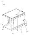
FIG. 4 is a perspective view of the power conversion apparatus 200. The power conversion apparatus 200 includes a housing 20. A housing upper cover 21 is placed on an upper surface of the housing 20. A housing lower cover 22 is placed on a lower surface of the housing 20. The housing upper cover 21 and the housing lower cover 22 are fixed to the housing 20 with screws.
A housing opening 20 a is provided in a side surface of the housing 20. The housing opening 20 a is provided for connecting a terminal of the power semiconductor module to outside. Another opening is provided in the side surface of the housing 20, and the alternating-current busbar 802 is protruded through the opening. An opening 20 e is provided in one surface of the side surface of the housing 20, the one surface facing to the surface in which the housing opening 20 a is provided (see FIG. 5). A coolant inlet pipe 30 a and a coolant outlet pipe 30 b (see FIG. 7) are provided to the housing 20.
A structure of the power conversion apparatus 200 of this embodiment has a substantially rectangular shape seen from a plan view, and therefore it is easy to attach the power conversion apparatus 200 to a vehicle or a motor generator.
FIG. 5 is an exploded perspective view of the power conversion apparatus 200. The power conversion apparatus 200 includes the boosting circuit 600 and the circuit 201 to which a boosted voltage is supplied. The housing 20 houses the boosting circuit 600 and the circuit 201 to which a boosted voltage is supplied. A flow channel through which a coolant flows is integrally provided with the housing 20, as described below. The circuit 201 to which a boosted voltage is supplied is placed on a side of the housing upper cover 21 and the boosting circuit 600 is placed on a side of the housing lower cover 22 with respect to the flow channel.
FIG. 6 is an exploded perspective view of the circuit 201, illustrated in FIG. 5, to which a boosted voltage is supplied. The circuit 201 to which a boosted voltage is supplied includes a driver circuit substrate 174 a, a control circuit substrate 172 a, the capacitor module 500, and power semiconductor modules 150 a. The driver circuit 174 of FIG. 2 is mounted on the driver circuit substrate 174 a. The control circuit 172 of FIG. 2 is mounted on the control circuit substrate 172 a.
A connector 172 b is provided on the control circuit substrate 172 a. The connector 172 b is connected to an xternal control apparatus, and transmits signals between the control circuit 172 provided on the control circuit substrate 172 a and the external control apparatus such as an upper control apparatus.
An opening 174 b is provided in the driver circuit substrate 174 a. The opening 174 b as well as the housing opening 20 a is provided to connect the terminal of the power semiconductor module to outside.
The driver circuit substrate 174 a is placed so that a main surface of the driver circuit substrate 174 a is orthogonal to a main surface of the control circuit substrate 172 a. The driver circuit substrate 174 a and the control circuit substrate 172 a are electrically connected by a flexible cable. With such a configuration, it is possible to achieve mounting at a high density in a limited space of the power conversion apparatus, and therefore a size of the whole power conversion apparatus can be reduced. Further, by using the flexible cable, it is possible to achieve electrical connection with an excellent vibration resistance.
The capacitor module 500 includes the direct-current connectors 138, capacitor-side positive electrode busbars 157 a, and capacitor-side negative electrode busbars 158 a. The direct-current connectors 138 are protruded to outside of the power conversion apparatus 200 through the opening 20 e. The capacitor-side positive electrode busbars 157 a and the capacitor-side negative electrode busbars 158 a are connected to the power semiconductor modules 150 a. In this embodiment, because three power semiconductor modules are provided, three sets of the capacitor-side positive electrode busbars 157 a and the capacitor-side negative electrode busbars 158 a are provided.
A circuit module holding member 23 to which a boosted voltage is supplied is a plate-like holding member for providing the driver circuit substrate 174 a, the control circuit substrate 172 a, the capacitor module 500, and the power semiconductor module 150 a.
On one side of a surface of the circuit module holding member 23 to which a boosted voltage is supplied, a power semiconductor module accommodating part 23 c is provided. The power semiconductor module accommodating part 23 c has a substantially rectangular parallelepiped.
In one side surface of the power semiconductor module accommodating part 23 c, a module insertion port 23 a is provided. The power semiconductor modules 150 a are inserted into the power semiconductor module accommodating part 23 c through the module insertion port 23 a. The power semiconductor modules 150 a of this embodiment have a flat shape and will be described below with reference to FIG. 7. The three power semiconductor modules 150 a are piled so as to be in parallel to a main surface of the circuit module holding member 23 to which a boosted voltage is supplied.
In this example, the module insertion port 23 a is a single large opening in order to simplify the flow channel, and therefore the three power semiconductor modules 150 a are inserted while being close to one another.
In the power semiconductor module accommodating part 23 c, coolant introduction ports 23 b are provided. The coolant introduction ports 23 b are openings that pass through the circuit module holding member 23 to which a boosted voltage is supplied. Although not shown in FIG. 6, the two coolant introduction ports 23 b are provided, i.e., an opening for introducing a coolant into the power semiconductor module accommodating part 23 c and an opening for discharging the coolant to outside of the power semiconductor module accommodating part 23 c are provided. That is, the power semiconductor module accommodating part 23 c has a coolant flow channel for cooling the power semiconductor modules 150 a.
An opening of the module insertion port 23 a is covered by the cover 5. The cover 5 has cover openings 5 a for allowing the terminals of the power semiconductor modules 150 a to pass therethrough, protrusion portions 5 b, and recessed portions 5 c.
The power semiconductor modules 150 a are connected to a part in which output-side alternating-current busbars 159 a, the current sensor 180, and the alternating-current busbars 802 are integrally provided. Alternating-current power converted from direct-current power by the power semiconductor modules is outputted by the alternating-current busbars 802.
The capacitor module 500 is placed on a surface of the circuit module holding member 23 to which a boosted voltage is supplied. The capacitor module 500 is placed on a side portion of the power semiconductor module accommodating part 23 c. The control circuit substrate 172 a is placed on the capacitor module 500 and the power semiconductor module accommodating part 23 c so as to mount on the capacitor module 500 and the power semiconductor module accommodating part 23 c.
Note that the capacitor-side positive electrode busbars 157 a and the capacitor-side negative electrode busbars 158 a generate heat in a case where a large current is flown, and therefore it is necessary to prevent heat from intruding into the power semiconductor modules 150 a. In view of this, by providing the protrusion portions 5 b in the cover 5 for fixing the power semiconductor modules and bringing the protrusion portions 5 b into thermal contact with the busbars, it is possible to reduce intrusion of heat into the power semiconductor modules 150 a. In a case where the cover 5 is made from metal material, the protrusion portions 5 b are brought into thermal contact via an insulating layer, however, as material of the cover, insulating material such as resin can be also used.
As described above, the circuit 201 to which a boosted voltage is supplied is structured as an independent module by mounting the whole circuit 201 (power semiconductor module 150 a, capacitor module 500, etc.) to which a boosted voltage is supplied on the circuit module holding member 23 to which a boosted voltage is supplied. Thus, the module constituting the circuit 201 to which a boosted voltage is supplied, a module constituting the boosting circuit 600, the housing upper cover 21, and the housing lower cover 22 can be stacked and therefore can be easily produced.
FIG. 7 is a perspective view and a sectional view of the power semiconductor module 150 a. The power semiconductor module 150 a includes a metal case 40 having a flat shape. A heat sink 7 a is subjected to metallic bonding onto one surface of the metal case 40 and a heat sink 7 b is subjected to metallic bonding onto the other surface thereof. Cooling fins 8 are provided on the heat sinks 7 a and 7 b of the metal case 40.
The metal case 40 includes a part 40 a for holding the heat sinks 7 a and 7 b and a sealing material holding portion 40 b. In a case where, for example, an 0 ring is used as sealing material, a groove for the O ring is processed in the sealing material holding portion 40 b. The sealing material holding portion 40 b has a curved surface without edges in order to prevent damage to the O ring.
Herein, a distance between tips of the cooling fins 8 provided on the heat sink 7 a and tips of the cooling fins 8 provided on the heat sink 7 b is defined as a heat sink thickness 45 a. Further, a thickness of the sealing material holding portion 40 b is defined as a sealing material holding portion thickness 45 b. In this case, the sealing material holding portion thickness 45 b is provided to be smaller than the heat sink thickness 45 a.
The power semiconductor module 150 a accommodates the vertical arm series circuits 150 illustrated in FIG. 3 in the metal case 40. A control pin, a signal pin, a temperature output pin, etc. 160, the positive electrode busbar 157 a, a negative electrode busbar 158 b, and an alternating-current busbar 159 b are protruded from the metal case 40. The control pin, the signal pin, the temperature output pin, etc. 160 are connected to the control circuit substrate 172 via the driver circuit substrate 174 a, and receive and output a gate signal, an emitter sense signal, and information on the temperature sensor included in the power semiconductor. The positive electrode busbar 157 a is connected to the capacitor-side positive electrode busbar 157 a. The negative electrode busbar 158 b is connected to the capacitor-side negative electrode busbar 158 a. The alternating-current busbar 159 b is connected to the output-side alternating-current busbar 159 a. As described above, in order to easily connect the control pin, the signal pin, the temperature output pin, etc. 160 to outside, the opening 174 b is provided in the driver circuit substrate 174 a and the housing opening 20 a is provided in the housing 20.
In order to reduce costs, the metal case 40 may be an integrated container produced by molding a can shape and forming a heat-radiation fin part 7 and the casing portion 40 a by forging.
FIG. 8 is a perspective view of a set of constituent members of the flow channel. FIG. 8(a) is a perspective view, seen from a lower surface, of the power conversion apparatus 200 from which the housing lower cover 22 and the boosting circuit 600 are removed. In the power conversion apparatus 200 of this embodiment, a coolant flown from the coolant inlet pipe 30 a is flown through a first flow channel 20 b illustrated in FIG. 8. The first flow channel 20 b is a space that is obtained by covering an in-housing opening 20 d integrally provided with the housing 20 with the use of the circuit module holding member 23 to which a boosted voltage is supplied (see FIG. 9).
Subsequently, the coolant passes through the coolant introduction port 23 b of the power semiconductor module accommodating part 23 c, and is introduced into the power semiconductor module accommodating part 23 c. The coolant cools the power semiconductor module 150 a in the power semiconductor module accommodating part 23 c, and is discharged from the power semiconductor module accommodating part 23 c through the other coolant introduction port 23 b. Thereafter, the coolant is flown through a second flow channel 20 c, and is discharged from the coolant outlet pipe 30 b.
The coolant flown through the first flow channel 20 b and the second flow channel 20 c also cools, via the circuit module holding member 23 to which a boosted voltage is supplied, the capacitor module 500 placed to be opposite to the circuit module holding member 23 to which a boosted voltage is supplied.
FIG. 9 is a sectional view taken along the line C-C′ of FIG. 4. As illustrated in FIG. 9, the circuit module holding member 23 to which a boosted voltage is supplied is placed on one side and the boosting circuit 600 is placed on the other side with respect to the coolant flow channel. As described above, the coolant flow channel is provided by covering the in-housing opening 20 d integrally provided with the housing 20 with the use of the circuit module holding member 23 to which a boosted voltage is supplied. In other words, the housing 20 of the power conversion apparatus 200 according to this embodiment functions not only as a structural member for holding the circuit module holding member 23 to which a boosted voltage is supplied and on which the power semiconductor module, the capacitor module, and the like are mounted, but also as a flow channel forming body for cooling those members. With this configuration, it is possible to efficiently cool the power semiconductor module 150 having a large heating value, the capacitor module 500, and the boosting circuit 600.
The driver circuit substrate 174 a and the control circuit substrate 172 a are thermally connected to the housing 20 made from metal and the circuit module holding member 23 to which a boosted voltage is supplied, and heat is released to a cooling medium in the flow channel via the metal member having high thermal conductivity.
As illustrated in FIG. 9, the recessed portions 5 c are provided in the cover 5 in accordance with placement with the power semiconductor modules 150 a. The openings 5 a are provided in bottom surface portions of the recessed portions 5 c, and a module-side positive electrode busbars 157 b and the module-side negative electrode busbars 158 b that are terminals of the power semiconductor modules 150 a pass through the openings 5 a. The sealing material holding portion 40 b of each of the power semiconductor modules 150 a and an inner wall of each of the recessed portions 5 c of the cover 5 form an airtight structure. That is, the recessed portion 5 c of the cover 5 is provided to be fitted into the sealing material holding portion 40 b of the power semiconductor module 150 a. Further, sealing material is provided between the sealing material holding portion 40 b and a recessed portion c of the cover 5. Therefore, outflow of a coolant flown through the power semiconductor module accommodating part 23 c to outside is prevented and inflow of the coolant into the power semiconductor module is prevented.
Therefore, for example, in a case where the cover 5 is fastened to the housing with the use of bolts, the sealing material is pressed on a side surface regardless of a pressing force of the bolts, and therefore it is unnecessary to provide a bolt in the flow channel in the periphery of the power semiconductor module. This makes it possible to reduce the number of bolts. Further, even in a case where a size in a vertical direction is small because of production variation of power semiconductor modules, the sealing material is always pressed on the side surface, and therefore it is possible to reduce occurrence of fluid leakage to outside and bypass flow in a local space inside the module. This improves sealing reliability. By providing the recessed portions in the cover, it is possible to avoid to perform sealing on a side surface of a thick plate. In a case where the thick plate is used, it is difficult to reduce a weight, and there is also a problem in a quake-resistant structure because a center of gravity thereof becomes high. By providing the recessed portions, it is possible to apply rigidity only to a necessary part and to reduce the weight.
Further, in this embodiment, the three power semiconductor modules 150 a are placed to be close to one another in the power semiconductor module accommodating part 23 c. In a coolant flow channel provided by stacking the power semiconductor modules 150 a, in order to prevent bypass flow of a coolant, it is preferable to decrease a space between the cooling fins 8 of a power semiconductor module and the cooling fins 8 of another power semiconductor module as much as possible.
The recessed portions 5 c are provided in the cover 5 to correspond to the power semiconductor modules 150 a. Therefore, the three recessed portions 5 c are provided to be adjacent to one another. In order to apply rigidity to the cover 5 and also to obtain airtightness, the recessed portions 5 c adjacent to one another need to have appropriate distances.
Therefore, in this embodiment, as illustrated in FIG. 7, the sealing material holding portion 40 b is provided so that the sealing material holding portion thickness 45 b is smaller than the heat sink thickness 45 a. Therefore, it is possible to reduce a size of the power module accommodating part 23 c without deteriorating properties such as prevention of bypass flow and obtaining of airtightness, and such reduction in size eventually contributes to reduce the size of the whole power conversion apparatus 200.
In the above embodiment, a shape of the fins of the heat sink 7 is a pin fin, however, may be, for example, a straight fin or a corrugated fin.
The above embodiment has described an example of an in-vehicle power conversion apparatus provided in an electric vehicle and a hybrid electric vehicle, however, the invention can be similarly applied as long as the power conversion apparatus has a cooling structure in which a power module is immersed in a cooling medium.
Note that, in the above example, the three power semiconductor modules 150 a are placed in parallel, however, two-branched flow channels can be achieved by placing flow channels in series instead of achieving four-branched flow channels by placing the flow channels in parallel. By decreasing the number of branches in a system that can even allow a large pressure loss, a flow rate per module is increased and thermal conductivity becomes large, and therefore it is possible to improve coolability.
In the above example, the three power semiconductor modules 150 a are inserted while being close to one another and being adjacent to one another, however, a wall of a holding member for providing a power semiconductor module accommodating space may be interposed between a power semiconductor module and another power semiconductor module. By interposing the wall between the power semiconductor module and the another power semiconductor module, it is unnecessary to share the flow channel of the heat sink part of the adjacent power semiconductor modules 150 a. Therefore, sectional areas of the branched flow channels become equal and variation of flow distribution to the branched flow channels is reduced. Thus, uniform cooling can be easily performed.
In the above example, all the main terminals (positive electrode busbar 157 b, negative electrode busbar 158 b, and alternating-current busbar 159 b) and the control pin, the signal pin, the temperature output pin, etc. 160 are taken out from one surface, however, the control pin, the signal pin, the temperature output pin, etc. 160 may be taken out from a surface opposite to a surface from which the main terminals are taken out. With this, it is possible to separate weak current system pins from strong current system main terminals, and therefore it is possible to reduce noises of signals. In a case where a plurality of modules are mounted, occurrence of fluid leakage can be prevented by applying a side-surface sealing structure of the invention, even if a size in a vertical direction of only one particular module is varied.
The above embodiments may be solely implemented or combined with each other because effects of the embodiments can be solely obtained or multiplied. Further, the invention is not limited to the above embodiments as long as the invention has features.
REFERENCE SIGNS LIST
  • 1: sealing material
  • 2: ring-like member for holding horizontally separated heat sinks
  • 3 a: right-side separated heat sink
  • 3 b: left-side separated heat sink
  • 4: wall surface of housing
  • 5: cover
  • 5 a: opening
  • 5 b: protrusion portion
  • 5 c: recessed portion
  • 6: second cover
  • 7: heat sink
  • 7 a: right-side integrated heat sink
  • 7 b: left-side integrated heat sink
  • 7 c: integrated flange
  • 8: cooling fin
  • 11: fluid leakage
  • 12: bypass flow in sheet direction
  • 13: bypass flow
  • 20: housing
  • 20 a: housing opening
  • 20 b: first flow channel
  • 20 c: second flow channel
  • 20 d: in-housing opening
  • 20 e: housing opening
  • 21: housing upper cover
  • 22: housing lower cover
  • 23: circuit module holding member to which a boosted voltage is supplied
  • 23 a: module insertion port
  • 23 b: coolant introduction port
  • 23 c: power semiconductor module accommodating part
  • 30 a: coolant inlet pipe
  • 30 b: coolant outlet pipe
  • 40: metal case
  • 40 a: heat sink holding portion
  • 40 b: sealing material holding portion
  • 45 a: heat sink thickness
  • 45 b: sealing material holding portion thickness
  • 130: thick part
  • 131: thin part
  • 136: battery
  • 138: direct-current connector
  • 140, 142: inverter circuit
  • 144: heat-radiation fin group
  • 150: vertical arm series circuit
  • 150 a: 2 in 1 power semiconductor module
  • 153: collector electrode of IGBT of upper arm
  • 154: gate electrode
  • 155: signal emitter electrode
  • 156: diode of upper arm
  • 157: positive electrode terminal
  • 157 a: capacitor-side positive electrode busbar
  • 157 b: module-side positive electrode busbar
  • 158: negative electrode terminal
  • 158 a: capacitor-side negative electrode busbar
  • 158 b: module-side negative electrode busbar
  • 159, 188: alternating-current terminal
  • 159 a: output-side alternating-current busbar
  • 159 b: module-side alternating-current busbar
  • 160: control pin, signal pin, temperature output pin, etc.
  • 163: collector electrode of IGBT of lower arm
  • 164: gate electrode
  • 165: signal emitter electrode
  • 166: diode of lower arm
  • 169: intermediate electrode
  • 172: control circuit
  • 172 a: control circuit substrate
  • 172 b: connector on control circuit substrate
  • 174: driver circuit
  • 174 a: driver circuit substrate
  • 174 b: opening
  • 180: current sensor
  • 200: power conversion apparatus
  • 201: circuit to which a boosted voltage is supplied
  • 328: IGBT of upper arm
  • 330: IGBT of lower arm
  • 500: capacitor module
  • 504: negative-electrode side capacitor terminal
  • 506: positive-electrode side capacitor terminal
  • 508: negative-electrode side power source terminal
  • 509: positive-electrode side power source terminal
  • 600: boosting circuit
  • 802: alternating-current busbar

Claims (7)

The invention claimed is:
1. A power conversion apparatus, comprising:
a power semiconductor module for converting direct-current power into alternating-current power;
a first flow channel forming body for housing the power semiconductor module; and
a cover for fixing the power semiconductor module to the first flow channel forming body, wherein:
the power semiconductor module includes a power semiconductor element, main terminals electrically connected to the power semiconductor element, and a case for housing the power semiconductor element;
the cover has a recessed portion and an opening provided in a bottom surface portion of the recessed portion;
the power semiconductor module is placed to be fitted into the recessed portion;
the power semiconductor module is fixed to the cover so that the main terminals pass through the opening; and
the case and an inner wall of the recessed portion have an airtight structure.
2. The power conversion apparatus according to claim 1, wherein:
the first flow channel forming body includes a power semiconductor module accommodating part;
the power semiconductor module accommodating part has a module insertion port and a coolant introduction port;
the power semiconductor module is accommodated in the power semiconductor module accommodating part through the module insertion port; and
the case is directly contacted with a cooling coolant flown from the coolant introduction port.
3. The power conversion apparatus according to claim 1, wherein:
the case has a fin on an outer surface of the case;
the case is such that a thickness of a part in contact with the inner wall of the recessed portion is smaller than a thickness of a part on which the fin is provided, the thickness including a height of the fin.
4. The power conversion apparatus according to claim 1, wherein:
a side surface of the case for housing the power semiconductor element has a curved surface and has a substantially elliptical shape.
5. The power conversion apparatus according to claim 1, further comprising:
a capacitor module for smoothing the direct-current power;
a driver circuit substrate; and
a control circuit substrate, wherein
the capacitor module, the driver circuit substrate, and the control circuit substrate are provided in the first flow channel forming body.
6. The power conversion apparatus according to claim 1, further comprising:
a capacitor module for smoothing the direct-current power;
a boosting circuit for boosting the direct-current power; and
a housing for housing the power semiconductor module, the capacitor module, and the boosting circuit, wherein:
the housing has a second flow channel forming body integrally provided with the housing inside the housing;
the power semiconductor module and the capacitor module are placed on one side of the second flow channel forming body; and
the boosting circuit is placed on the other side of the second flow channel forming body.
7. The power conversion apparatus according to claim 1, wherein
a conductor plate for connecting the power semiconductor module to another member is closely attached to the case including a protrusion portion.
US14/422,381 2012-09-28 2013-07-24 Power conversion apparatus Expired - Fee Related US9510487B2 (en)

Applications Claiming Priority (3)

Application Number Priority Date Filing Date Title
JP2012-215457 2012-09-28
JP2012215457A JP5851372B2 (en) 2012-09-28 2012-09-28 Power converter
PCT/JP2013/069972 WO2014050277A1 (en) 2012-09-28 2013-07-24 Power conversion apparatus

Publications (2)

Publication Number Publication Date
US20150223366A1 US20150223366A1 (en) 2015-08-06
US9510487B2 true US9510487B2 (en) 2016-11-29

Family

ID=50387691

Family Applications (1)

Application Number Title Priority Date Filing Date
US14/422,381 Expired - Fee Related US9510487B2 (en) 2012-09-28 2013-07-24 Power conversion apparatus

Country Status (5)

Country Link
US (1) US9510487B2 (en)
JP (1) JP5851372B2 (en)
CN (1) CN104584409B (en)
DE (1) DE112013003890T5 (en)
WO (1) WO2014050277A1 (en)

Cited By (1)

* Cited by examiner, † Cited by third party
Publication number Priority date Publication date Assignee Title
US20160241155A1 (en) * 2015-02-13 2016-08-18 Denso Corporation Power conversion apparatus

Families Citing this family (23)

* Cited by examiner, † Cited by third party
Publication number Priority date Publication date Assignee Title
US10131042B2 (en) 2013-10-21 2018-11-20 Milwaukee Electric Tool Corporation Adapter for power tool devices
US10080313B2 (en) * 2014-01-27 2018-09-18 Hitachi, Ltd. Power module and method for manufacturing the same
EP2931012A1 (en) * 2014-04-07 2015-10-14 Siemens Aktiengesellschaft Subsea power cell arrangement
JP6382657B2 (en) * 2014-09-18 2018-08-29 株式会社東芝 Power converter
KR101755769B1 (en) 2014-10-29 2017-07-07 현대자동차주식회사 Dual side cooling power module and Method for manufacturing the same
WO2016076040A1 (en) * 2014-11-13 2016-05-19 日立オートモティブシステムズ株式会社 Power conversion device
JP6481974B2 (en) * 2014-12-08 2019-03-13 パナソニックIpマネジメント株式会社 Capacitor and inverter
JP6149029B2 (en) * 2014-12-24 2017-06-14 本田技研工業株式会社 Inverter unit
WO2016204257A1 (en) * 2015-06-17 2016-12-22 富士電機株式会社 Power semiconductor module, flow path member, and power-semiconductor-module structure
WO2017068719A1 (en) * 2015-10-23 2017-04-27 日産自動車株式会社 Rotating electric machine device
CN105469943A (en) * 2015-12-28 2016-04-06 人民电器集团江苏斯诺成套设备工程有限公司 Radiating tube oil leakage prevention mechanism for energy-saving oil-immersed transformer
KR102048478B1 (en) * 2018-03-20 2019-11-25 엘지전자 주식회사 Power module of double-faced cooling and method for manufacturing thereof
KR102570579B1 (en) * 2018-07-13 2023-08-24 엘지전자 주식회사 Refrigerator
JP6717347B2 (en) * 2018-07-25 2020-07-01 株式会社デンソー Power converter
GB2577262B (en) * 2018-09-18 2022-06-29 Mclaren Automotive Ltd Method of cooling battery cells
CN113228482B (en) * 2018-12-26 2024-03-08 松下知识产权经营株式会社 Power conversion device
DE102019104962B4 (en) * 2019-02-27 2024-02-15 Lisa Dräxlmaier GmbH METHOD FOR PRODUCING A SWITCH BOX, IN PARTICULAR A HIGH VOLTAGE SWITCH BOX, FOR AN ELECTRICALLY DRIVEN MOTOR VEHICLE AND SWITCH BOX
JP7151599B2 (en) * 2019-04-08 2022-10-12 株式会社デンソー power converter
CN114073173A (en) * 2019-06-24 2022-02-18 沃尔沃建筑设备公司 Power converter assembly and power system
CN112750607A (en) 2019-10-31 2021-05-04 台达电子企业管理(上海)有限公司 Transformer and power module with same
CN112821722B (en) * 2019-10-31 2022-07-19 台达电子企业管理(上海)有限公司 Power conversion system
CN112751473B (en) 2019-10-31 2021-11-05 台达电子企业管理(上海)有限公司 Power module
JP2022160271A (en) * 2021-04-06 2022-10-19 三菱重工業株式会社 Housing and power conversion device

Citations (14)

* Cited by examiner, † Cited by third party
Publication number Priority date Publication date Assignee Title
US20030133267A1 (en) * 2002-01-16 2003-07-17 Beihoff Bruce C. Cooled electrical terminal assembly and device incorporating same
US20030173839A1 (en) * 2002-03-15 2003-09-18 Denso Corporation Liquid-cooled rotary electric machine integrated with an inverter
US20040061138A1 (en) 2002-09-26 2004-04-01 Mitsubishi Denki Kabushiki Kaisha Power semiconductor device with high radiating efficiency
US20060096299A1 (en) * 2004-11-11 2006-05-11 Denso Corporation Semiconductor device
JP2006202899A (en) 2005-01-19 2006-08-03 Toyota Motor Corp Semiconductor cooling apparatus
US20080117602A1 (en) * 2006-11-20 2008-05-22 Korich Mark D Power inverter having liquid cooled capacitor and low inductance bus structure
US20090040724A1 (en) * 2007-08-09 2009-02-12 Hitachi, Ltd. Power inverter
US20090231811A1 (en) * 2008-03-11 2009-09-17 Hitachi. Ltd. Electric Power Conversion Apparatus
US20100025126A1 (en) * 2008-07-29 2010-02-04 Hitachi, Ltd. Power Conversion Apparatus and Electric Vehicle
US7710721B2 (en) * 2006-04-27 2010-05-04 Hitachi, Ltd. Power inverter
JP2010110143A (en) 2008-10-31 2010-05-13 Hitachi Automotive Systems Ltd Power conversion device and electric vehicle
JP2011216754A (en) 2010-04-01 2011-10-27 Hitachi Automotive Systems Ltd Power module, and power converter using the same
US20110310585A1 (en) * 2010-06-21 2011-12-22 Hitachi Automotive Systems, Ltd. Power Semiconductor Device and Power Conversion Device
US8094454B2 (en) 2009-11-23 2012-01-10 Delphi Technologies, Inc. Immersion cooling apparatus for a power semiconductor device

Family Cites Families (2)

* Cited by examiner, † Cited by third party
Publication number Priority date Publication date Assignee Title
JP4988665B2 (en) * 2008-08-06 2012-08-01 日立オートモティブシステムズ株式会社 Semiconductor device and power conversion device using the semiconductor device
JP5481148B2 (en) * 2009-10-02 2014-04-23 日立オートモティブシステムズ株式会社 Semiconductor device, power semiconductor module, and power conversion device including power semiconductor module

Patent Citations (16)

* Cited by examiner, † Cited by third party
Publication number Priority date Publication date Assignee Title
US20030133267A1 (en) * 2002-01-16 2003-07-17 Beihoff Bruce C. Cooled electrical terminal assembly and device incorporating same
US20030173839A1 (en) * 2002-03-15 2003-09-18 Denso Corporation Liquid-cooled rotary electric machine integrated with an inverter
US20040061138A1 (en) 2002-09-26 2004-04-01 Mitsubishi Denki Kabushiki Kaisha Power semiconductor device with high radiating efficiency
JP2004119667A (en) 2002-09-26 2004-04-15 Mitsubishi Electric Corp Semiconductor device for electric power
US20060096299A1 (en) * 2004-11-11 2006-05-11 Denso Corporation Semiconductor device
JP2006202899A (en) 2005-01-19 2006-08-03 Toyota Motor Corp Semiconductor cooling apparatus
US7710721B2 (en) * 2006-04-27 2010-05-04 Hitachi, Ltd. Power inverter
US20080117602A1 (en) * 2006-11-20 2008-05-22 Korich Mark D Power inverter having liquid cooled capacitor and low inductance bus structure
US20090040724A1 (en) * 2007-08-09 2009-02-12 Hitachi, Ltd. Power inverter
US20090231811A1 (en) * 2008-03-11 2009-09-17 Hitachi. Ltd. Electric Power Conversion Apparatus
US20100025126A1 (en) * 2008-07-29 2010-02-04 Hitachi, Ltd. Power Conversion Apparatus and Electric Vehicle
JP2010110143A (en) 2008-10-31 2010-05-13 Hitachi Automotive Systems Ltd Power conversion device and electric vehicle
US20110299265A1 (en) 2008-10-31 2011-12-08 Kinya Nakatsu Power Module, Power Converter Device, and Electrically Powered Vehicle
US8094454B2 (en) 2009-11-23 2012-01-10 Delphi Technologies, Inc. Immersion cooling apparatus for a power semiconductor device
JP2011216754A (en) 2010-04-01 2011-10-27 Hitachi Automotive Systems Ltd Power module, and power converter using the same
US20110310585A1 (en) * 2010-06-21 2011-12-22 Hitachi Automotive Systems, Ltd. Power Semiconductor Device and Power Conversion Device

Non-Patent Citations (1)

* Cited by examiner, † Cited by third party
Title
International Search Report (PCT/ISA/210) dated Nov. 5, 2013, with English translation (Four (4) pages).

Cited By (4)

* Cited by examiner, † Cited by third party
Publication number Priority date Publication date Assignee Title
US20160241155A1 (en) * 2015-02-13 2016-08-18 Denso Corporation Power conversion apparatus
US9735700B2 (en) * 2015-02-13 2017-08-15 Denso Corporation Power conversion apparatus
US20170317605A1 (en) * 2015-02-13 2017-11-02 Denso Corporation Power conversion apparatus
US10135356B2 (en) * 2015-02-13 2018-11-20 Denso Corporation Power conversion apparatus

Also Published As

Publication number Publication date
DE112013003890T5 (en) 2015-04-16
CN104584409B (en) 2017-01-18
JP5851372B2 (en) 2016-02-03
US20150223366A1 (en) 2015-08-06
JP2014072939A (en) 2014-04-21
WO2014050277A1 (en) 2014-04-03
CN104584409A (en) 2015-04-29

Similar Documents

Publication Publication Date Title
US9510487B2 (en) Power conversion apparatus
US10512181B2 (en) Power semiconductor device and power conversion device
US9596782B2 (en) Power converter with cooling board
US9585292B2 (en) Power converter
US9474191B2 (en) Power semiconductor module
US9078376B2 (en) Power conversion device
US9301434B2 (en) Power conversion apparatus
US9246408B2 (en) Power conversion apparatus
US9438088B2 (en) Rotating electrical machine unit with a power inverter having a ring-shaped casing
US9419535B2 (en) Electric power converter
US20130094269A1 (en) Power Conversion Apparatus
WO2013018620A1 (en) Power conversion apparatus
WO2013164933A1 (en) Inverter device
JP5802629B2 (en) Power converter
JP6219442B2 (en) Power converter
JP5925863B2 (en) Power converter
CN115398621A (en) Power conversion device

Legal Events

Date Code Title Description
AS Assignment

Owner name: HITACHI AUTOMOTIVE SYSTEMS, LTD., JAPAN

Free format text: ASSIGNMENT OF ASSIGNORS INTEREST;ASSIGNORS:HORIUCHI, KEISUKE;NISHIHARA, ATSUO;NAKATSU, KINYA;AND OTHERS;SIGNING DATES FROM 20141217 TO 20150106;REEL/FRAME:035013/0443

STCF Information on status: patent grant

Free format text: PATENTED CASE

FEPP Fee payment procedure

Free format text: MAINTENANCE FEE REMINDER MAILED (ORIGINAL EVENT CODE: REM.); ENTITY STATUS OF PATENT OWNER: LARGE ENTITY

LAPS Lapse for failure to pay maintenance fees

Free format text: PATENT EXPIRED FOR FAILURE TO PAY MAINTENANCE FEES (ORIGINAL EVENT CODE: EXP.); ENTITY STATUS OF PATENT OWNER: LARGE ENTITY

STCH Information on status: patent discontinuation

Free format text: PATENT EXPIRED DUE TO NONPAYMENT OF MAINTENANCE FEES UNDER 37 CFR 1.362

FP Lapsed due to failure to pay maintenance fee

Effective date: 20201129